WO2021172089A1 - 光透過性積層体の検査方法 - Google Patents
光透過性積層体の検査方法 Download PDFInfo
- Publication number
- WO2021172089A1 WO2021172089A1 PCT/JP2021/005643 JP2021005643W WO2021172089A1 WO 2021172089 A1 WO2021172089 A1 WO 2021172089A1 JP 2021005643 W JP2021005643 W JP 2021005643W WO 2021172089 A1 WO2021172089 A1 WO 2021172089A1
- Authority
- WO
- WIPO (PCT)
- Prior art keywords
- light
- transmitting laminate
- laminate
- transmitting
- defect
- Prior art date
- Legal status (The legal status is an assumption and is not a legal conclusion. Google has not performed a legal analysis and makes no representation as to the accuracy of the status listed.)
- Ceased
Links
Images


Classifications
-
- G—PHYSICS
- G01—MEASURING; TESTING
- G01N—INVESTIGATING OR ANALYSING MATERIALS BY DETERMINING THEIR CHEMICAL OR PHYSICAL PROPERTIES
- G01N21/00—Investigating or analysing materials by the use of optical means, i.e. using sub-millimetre waves, infrared, visible or ultraviolet light
- G01N21/84—Systems specially adapted for particular applications
- G01N21/88—Investigating the presence of flaws or contamination
- G01N21/95—Investigating the presence of flaws or contamination characterised by the material or shape of the object to be examined
- G01N21/958—Inspecting transparent materials or objects, e.g. windscreens
-
- B—PERFORMING OPERATIONS; TRANSPORTING
- B32—LAYERED PRODUCTS
- B32B—LAYERED PRODUCTS, i.e. PRODUCTS BUILT-UP OF STRATA OF FLAT OR NON-FLAT, e.g. CELLULAR OR HONEYCOMB, FORM
- B32B7/00—Layered products characterised by the relation between layers; Layered products characterised by the relative orientation of features between layers, or by the relative values of a measurable parameter between layers, i.e. products comprising layers having different physical, chemical or physicochemical properties; Layered products characterised by the interconnection of layers
- B32B7/02—Physical, chemical or physicochemical properties
- B32B7/023—Optical properties
-
- B—PERFORMING OPERATIONS; TRANSPORTING
- B32—LAYERED PRODUCTS
- B32B—LAYERED PRODUCTS, i.e. PRODUCTS BUILT-UP OF STRATA OF FLAT OR NON-FLAT, e.g. CELLULAR OR HONEYCOMB, FORM
- B32B7/00—Layered products characterised by the relation between layers; Layered products characterised by the relative orientation of features between layers, or by the relative values of a measurable parameter between layers, i.e. products comprising layers having different physical, chemical or physicochemical properties; Layered products characterised by the interconnection of layers
- B32B7/04—Interconnection of layers
- B32B7/12—Interconnection of layers using interposed adhesives or interposed materials with bonding properties
-
- G—PHYSICS
- G01—MEASURING; TESTING
- G01B—MEASURING LENGTH, THICKNESS OR SIMILAR LINEAR DIMENSIONS; MEASURING ANGLES; MEASURING AREAS; MEASURING IRREGULARITIES OF SURFACES OR CONTOURS
- G01B11/00—Measuring arrangements characterised by the use of optical techniques
-
- G—PHYSICS
- G01—MEASURING; TESTING
- G01B—MEASURING LENGTH, THICKNESS OR SIMILAR LINEAR DIMENSIONS; MEASURING ANGLES; MEASURING AREAS; MEASURING IRREGULARITIES OF SURFACES OR CONTOURS
- G01B11/00—Measuring arrangements characterised by the use of optical techniques
- G01B11/22—Measuring arrangements characterised by the use of optical techniques for measuring depth
-
- G—PHYSICS
- G01—MEASURING; TESTING
- G01M—TESTING STATIC OR DYNAMIC BALANCE OF MACHINES OR STRUCTURES; TESTING OF STRUCTURES OR APPARATUS, NOT OTHERWISE PROVIDED FOR
- G01M11/00—Testing of optical apparatus; Testing structures by optical methods not otherwise provided for
-
- G—PHYSICS
- G01—MEASURING; TESTING
- G01N—INVESTIGATING OR ANALYSING MATERIALS BY DETERMINING THEIR CHEMICAL OR PHYSICAL PROPERTIES
- G01N21/00—Investigating or analysing materials by the use of optical means, i.e. using sub-millimetre waves, infrared, visible or ultraviolet light
- G01N21/84—Systems specially adapted for particular applications
- G01N21/88—Investigating the presence of flaws or contamination
- G01N21/8851—Scan or image signal processing specially adapted therefor, e.g. for scan signal adjustment, for detecting different kinds of defects, for compensating for structures, markings, edges
-
- G—PHYSICS
- G01—MEASURING; TESTING
- G01N—INVESTIGATING OR ANALYSING MATERIALS BY DETERMINING THEIR CHEMICAL OR PHYSICAL PROPERTIES
- G01N21/00—Investigating or analysing materials by the use of optical means, i.e. using sub-millimetre waves, infrared, visible or ultraviolet light
- G01N21/84—Systems specially adapted for particular applications
- G01N21/88—Investigating the presence of flaws or contamination
- G01N21/94—Investigating contamination, e.g. dust
-
- G—PHYSICS
- G01—MEASURING; TESTING
- G01N—INVESTIGATING OR ANALYSING MATERIALS BY DETERMINING THEIR CHEMICAL OR PHYSICAL PROPERTIES
- G01N21/00—Investigating or analysing materials by the use of optical means, i.e. using sub-millimetre waves, infrared, visible or ultraviolet light
- G01N21/84—Systems specially adapted for particular applications
- G01N21/88—Investigating the presence of flaws or contamination
- G01N21/8851—Scan or image signal processing specially adapted therefor, e.g. for scan signal adjustment, for detecting different kinds of defects, for compensating for structures, markings, edges
- G01N2021/8854—Grading and classifying of flaws
- G01N2021/8861—Determining coordinates of flaws
-
- G—PHYSICS
- G01—MEASURING; TESTING
- G01N—INVESTIGATING OR ANALYSING MATERIALS BY DETERMINING THEIR CHEMICAL OR PHYSICAL PROPERTIES
- G01N2201/00—Features of devices classified in G01N21/00
- G01N2201/10—Scanning
- G01N2201/108—Miscellaneous
- G01N2201/1087—Focussed scan beam, e.g. laser
Definitions
- the present invention relates to a method for inspecting a light transmissive laminate.
- the light-transmitting laminate for example, an optical member, an optical laminate, an optical film, a light-transmitting adhesive sheet
- an image display device eliminates foreign matter inside the laminate in order to prevent image display defects and the like.
- the foreign matter inspection is typically a transmission inspection performed while transporting a long web of a light transmissive laminate, and in the transmission inspection, foreign matter and / or defects can be recognized as dark spots.
- the display performance required for an image display device has become remarkably high, and as a result, the accuracy of foreign matter inspection of a light-transmitting laminate has also been remarkably required.
- the present invention has been made to solve the above problems, and a main object thereof is to provide a method for inspecting a light-transmitting laminate capable of detecting significantly minute foreign substances and / or defects as compared with the conventional ones. It is in.
- the transmission inspection is performed with the single-wafer light-transmitting laminate fixed in the air, and the defect of the light-transmitting laminate having a size of 8 ⁇ m to 50 ⁇ m is found.
- the detection of the defect is to focus the optical system at a predetermined magnification on the surface of the first main surface of the light transmissive laminate and scan the light transmissive laminate with the optical system.
- the optical system is used to shift the focal point of the optical system inward in the thickness direction from the surface of the first main surface of the light transmissive laminate by a predetermined distance.
- the detection of the defect is to scan the light transmissive laminate with the optical system by further shifting the focus of the optical system inward in the thickness direction of the light transmissive laminate by the predetermined distance. This includes repeating this a predetermined number of times to create an XY coordinate map of a predetermined number of defects.
- the detection of the defect measures the position of the defect in the thickness direction using an optical system having a magnification higher than the predetermined magnification only in the defect occurrence coordinates of the XY coordinate map of the integrated defect. Including doing.
- the measurement of the location of the defect in the thickness direction is to focus the high magnification optical system on the surface of the first main surface of the light transmissive laminate, and to focus the focus. This includes measuring the distance from the surface of the first main surface to the defect by moving the light transmissive laminate inward in the thickness direction.
- the predetermined distance is 10 ⁇ m to 100 ⁇ m.
- the predetermined magnification is 5 times or less.
- the high magnification is 10 times or more.
- the light transmissive laminate is selected from an optical film, an adhesive sheet, and a combination thereof.
- the optical film is selected from a polarizing plate, a retardation plate, and a laminate containing them.
- the thickness of the light-transmitting laminate is 300 ⁇ m or less. In one embodiment, in the above inspection method, a region in which the amount of variation in the thickness direction of the first main surface of the light transmissive laminate per 1000 ⁇ m scanning distance by the optical system having the predetermined magnification is within ⁇ 10 ⁇ m. Then, the above-mentioned defect is detected. In one embodiment, in the above inspection method, the above-mentioned defects are detected in a region where the bending angle of the light-transmitting laminate is within ⁇ 0.57 ° with respect to the horizontal direction.
- the above-mentioned defects are detected in a state where the above-mentioned light-transmitting laminate is laid horizontally.
- the above-mentioned drawbacks Detection is done in a state where the opposite ends, which are non-product regions in the light transmissive laminate, are fixed to a pair of support members that can be relatively close to each other or separated from each other.
- the pair of support members are slidable and urged in a direction away from each other.
- the light-transmitting laminate includes a pressure-sensitive adhesive layer, and the light-transmitting laminate is fixed to the pair of support members via the pressure-sensitive adhesive layer.
- the light-transmitting laminate is fixed via the pressure-sensitive adhesive layer via the pressure-sensitive adhesive layer exposed by peeling off a separator at one end of the light-transmitting laminate. This includes attaching to one support member, and then attaching to the other support member via the adhesive layer exposed by peeling off the separator at the other end.
- the light-transmitting laminate comprises a surface protective film that is detachably attached to at least one surface, and the inspection method attaches the light-transmitting laminate to the pair of support members. This includes temporarily peeling off the surface protective film after fixing.
- the inspection method is separate from the temporarily peeled surface protective film or the surface protective film on at least one surface of the light transmissive laminate after the detection of the defects.
- a light-transmitting laminate used in the above-mentioned method for inspecting a light-transmitting laminate.
- the light-transmitting laminate further includes at least one reflective protective film that is detachably temporarily attached to the first main surface side.
- the reflective protective film has a function of reflecting the irradiation light when the focus of the optical system having the predetermined magnification is aligned with the surface of the first main surface and transmitting the inspection light.
- the reflective protective film satisfies the following relationship: y ⁇ 0.0181x-11.142
- x is the absolute value of the detection wavelength in the wavelength region of 650 nm to 800 nm
- y is the absolute value of the reflectance.
- the light transmissive laminate further comprises a surface protective film that is detachably temporarily attached to the surface of the reflective protective film.
- the light-transmitting laminate further comprises a hard coat layer formed on the surface of the reflective protective film.
- the light transmissive laminate is provided with a recognition means capable of recognizing the inspected region after inspection.
- the method for inspecting a light-transmitting laminate by performing a transmission inspection in a state where the single-wafer light-transmitting laminate is fixed in a hollow shape, the light-transmitting laminate is much smaller than the conventional one (for example). , 8 ⁇ m size) and / or defects can be detected.
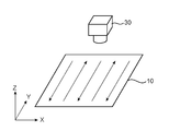
- FIG. 1 It is a schematic side view explaining an example of the permeation inspection in one Embodiment of this invention.
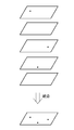
- (A) to (d) are schematic side views illustrating an example of a procedure of a method of fixing a light-transmitting laminate to a support member in detecting defects in a transmission inspection. It is the schematic explaining the focusing of the image pickup device in the detection of the defect of the transmission inspection. It is the schematic perspective view explaining the scanning of the XY plane of the light transmissive laminate by the image pickup element in the detection of the defect of the transmission inspection. It is a conceptual diagram explaining an example of the XY coordinate map of the defect in the detection of the defect of the transmission inspection.
- FIG. 1 is a schematic side view illustrating an example of a permeation inspection.
- the transmission inspection includes, for example, using an optical system to obtain an image of a light-transmitting laminated body 10 laid horizontally on a pair of support members 20, 20.
- the optical system is, for example, an image sensor 30 arranged on one side of the light-transmitting laminate 10 (upper in the illustrated example) to obtain an image of the light-transmitting laminate; and the other side of the light-transmitting laminate 10.
- the image sensor 30 includes a light source 40 which is arranged (lower in the illustrated example) and emits irradiation light for irradiating the light-transmitting laminated body 10.
- the image sensor 30 may be arranged below the light-transmitting laminate 10, and the light source 40 may be arranged above the light-transmitting laminate 10.
- the image sensor 30 captures a transmitted light (inspection light) image, and in the captured image, foreign matter and / or defects (hereinafter, may be simply referred to as foreign matter or defects depending on the context) are recognized as dark spots. obtain. A more specific embodiment of the permeation inspection will be described later.
- the light-transmitting laminate has a size of 8 ⁇ m to 50 ⁇ m, preferably 8 ⁇ m to 30 ⁇ m, more preferably 8 ⁇ m to 20 ⁇ m, still more preferably.
- foreign matter inspection of a light-transmitting laminate such as an optical film is performed while transporting a long web. According to such a foreign matter inspection, it is practically impossible to detect a small foreign matter (typically having a size of 50 ⁇ m or less).
- the light-transmitting laminate is cut into a single-wafer shape, and the transmission inspection is performed with the single-wafer-like light-transmitting laminate fixed in the air (that is, without mounting).
- the transmission inspection is performed with the single-wafer-like light-transmitting laminate fixed in the air (that is, without mounting).
- Light-transmitting laminates examples include any suitable light-transmitting laminates that require foreign matter inspection. Specific examples include an optical film, an adhesive sheet, and a combination thereof (for example, an optical film with an adhesive layer). Examples of the optical film include a polarizing plate, a retardation plate, a conductive film for a touch panel, a surface treatment film, and a laminate appropriately laminated according to the purpose (for example, an antireflection circular polarizing plate and a touch panel). A polarizing plate with a conductive layer).
- the pressure-sensitive adhesive sheet typically includes a pressure-sensitive adhesive and a release film temporarily attached to at least one side thereof.
- the light-transmitting laminate can typically be an optical film with an adhesive layer.
- the thickness of the light-transmitting laminate is preferably 300 ⁇ m or less, more preferably 280 ⁇ m or less, and further preferably 250 ⁇ m or less. According to the embodiment of the present invention, even in such a thin light-transmitting laminate, minute foreign matter can be detected satisfactorily.
- the lower limit of the thickness of the light-transmitting laminate can be, for example, 30 ⁇ m.
- the light-transmitting laminate can be produced, for example, by laminating each layer constituting the light-transmitting laminate by so-called roll-to-roll.
- the light-transmitting laminate has a first main surface and a second main surface.
- the first main surface is typically the surface opposite the image display cell to which the light transmissive laminate is attached;
- the second main surface is typically the surface on the image display cell side and more. In particular, it can be the surface of the pressure-sensitive adhesive layer.
- the produced long light-transmitting laminate is cut into a predetermined size and subjected to a foreign matter inspection.
- the size can typically be a size at which a plurality of final products can be obtained. After completion of the inspection, the light transmissive laminate can typically be cut to the final product size and shipped.
- a reflective protective film may be temporarily attached to the first main surface so as to be peelable.
- the autofocus of the image sensor may be on the first main surface of the light-transmitting laminate. Where it may not function, by temporarily attaching a reflective protective film, the autofocus of the image sensor can function well on the first main surface of the light transmissive laminate even in such a case. ..
- the reflective protective film typically has a function of reflecting irradiation light and transmitting inspection light when the optical system having a predetermined magnification is focused on the surface of the first main surface of the light transmissive laminate.
- the reflective protective film satisfies the following relationship: y ⁇ 0.0181x-11.142
- x is the absolute value of the detection wavelength in the wavelength region of 650 nm to 800 nm
- y is the absolute value of the reflectance.
- the reflective protective film may be composed of, for example, the cyclic olefin resin described in [0031] of JP-A-2019-099751.
- the cyclic olefin resin include polynorbornene.
- the cyclic olefin resin a commercially available product may be used. Specific examples of commercially available products include Zeonoa and Zeonex manufactured by Zeon Corporation, Arton manufactured by JSR, Appel manufactured by Mitsui Chemicals, and Topas manufactured by TOPAS ADVANCED Polymers.
- the cyclic olefin resin film preferably contains 50% by weight or more of the cyclic olefin resin.
- a hard coat layer may be formed on the surface of the reflective protective film. By forming the hard coat layer, it is possible to prevent scratches on the reflective protective film and foreign matter from adhering to the reflective protective film. Foreign matter and / or defects can be detected accurately.
- a plurality of reflective protective films may be temporarily attached depending on the planned number of inspections. For example, if a foreign matter inspection is scheduled twice, two reflective protective films can be attached together, and one outer reflective protective film can be peeled off before the second foreign matter inspection to reflect the inner surface. Since it is possible to prevent scratches on the sex protection film and foreign matter from adhering to the reflective protective film inside, it is possible to perform a plurality of foreign matter inspections with higher accuracy. Even when a plurality of inspections are scheduled, only one reflective protective film may be temporarily attached.
- the surface protective film may be temporarily attached to the surface of the reflective protective film (in the case where a plurality of reflective protective films are present, the surface of the outermost reflective protective film) so as to be peelable.
- the surface protective film By temporarily attaching the surface protective film, it is possible to prevent scratches on the reflective protective film and foreign matter from adhering to the reflective protective film, so that foreign matter inspection can be performed with higher accuracy.
- the surface protective film is typically stripped off during inspection. After the inspection is completed, the surface protective film peeled off at the time of the inspection may be temporarily attached to the surface of the light-transmitting laminate, or another surface protective film may be temporarily attached so as to be peelable.
- the reflective protective film and the surface protective film may be temporarily attached to the light-transmitting laminate by roll-to-roll (that is, before cutting), or may be temporarily attached after cutting.
- Embodiment C-1 Of the method for inspecting a light-transmitting laminate. Fixing in the hollow The following describes more specifically the detection of defects in the permeation inspection.
- the single-wafer light-transmitting laminate is fixed in the air as described above.
- the light-transmitting laminate can be fixed in the air by being laid horizontally on a pair of support members, for example, as shown in FIG. 1 above.
- the opposing ends which are non-product regions, can be fixed to the support member.
- the light-transmitting laminate includes a pressure-sensitive adhesive layer, and the light-transmitting laminate can be fixed to the support member via the pressure-sensitive adhesive layer.
- FIG. 2A the separator at one end 10c, which is a non-product region of the light-transmitting laminate, is peeled off and removed to expose the pressure-sensitive adhesive layer.
- the end portion 10c is attached to the support member 20 via the pressure-sensitive adhesive layer.
- the separator of the end portion 10d facing the end portion 10c which is a non-product region, is peeled off and removed to expose the pressure-sensitive adhesive layer, and the end portion 10d is exposed via the pressure-sensitive adhesive layer. It is attached to the support member 20. By sticking (the end portion of) the light-transmitting laminate to the support member with an adhesive layer, simple fixing is possible without using a fixing jig separately. When the ends 10c and 10d are bonded together, all separators are removed, as shown in FIG. 2 (c).
- the reflective protective film 50 and the surface protective film 60 not only prevent the generation of scratches on the light-transmitting laminate and / or the adhesion of foreign matter to the light-transmitting laminate, but also remove the separator and the end portion. It can also function as a reinforcing material when laminating. In this way, the light-transmitting laminate is laid horizontally on the support member.
- the surface protective film 60 is peeled off, and the light-transmitting laminate 10 to which the reflective protective film 50 is temporarily attached is subjected to a foreign matter inspection.
- the separator is peeled off by fixing the light-transmitting laminate to the support member and then peeling off the surface protective film (that is, by fixing the light-transmitting laminate to the support member with the surface-protective film temporarily attached). It is possible to maintain the rigidity (stiffness) of the light-transmitting laminated body even after this, and it becomes easy to handle. As a result, wrinkles and the like are prevented, so that foreign matter inspection can be performed with high accuracy, and minute foreign matter and / or defects can be accurately detected.
- a foreign matter inspection with the single-wafer light-transmitting laminate laid horizontally, the effects of fluttering and / or vibration of the transport device due to transport can be eliminated, so that after the surface protective film has been peeled off.
- foreign matter inspection can be performed with high accuracy, and minute foreign matter and / or defects can be accurately detected.
- peeling off the surface protective film foreign matter on the surface protective film is not detected, so that the foreign matter inspection can be performed with higher accuracy due to the synergistic effect with the above effect.
- a plurality of reflective protective films may be temporarily attached. In this case, the surface protective film is peeled off and removed at the first foreign matter inspection, and the reflective protective film can be peeled off one by one at each subsequent foreign matter inspection.
- the pair of support members 20, 20 are typically configured to be relatively close to each other or separated from each other.
- the support members are slidable and urged away from each other. Specifically, as shown in FIGS. 2 (b) to 2 (d), one of the support members (on the right side of the drawing in the illustrated example) is fixed, and the other (on the left side of the drawing in the illustrated example) is slidable. The other is urged by an elastic member (for example, a spring) in a direction of separation. With such a configuration, an appropriate tension is applied to the light-transmitting laminate, and the light-transmitting laminate is stretched.
- an elastic member for example, a spring
- both of the support members may be configured to be slidable, and both may be urged in a direction separated by the elastic member.
- defect detection is typically performed using an optical system (including an image sensor 30 and a light source 40) as shown in FIG.
- an optical system including an image sensor 30 and a light source 40
- the focus of the optical system (substantially, the image pickup device 30) having a predetermined magnification (hereinafter, may be referred to as a low magnification) is the first main focus of the light transmissive laminate 10. Align with the surface of surface 10a.
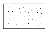
- the image sensor 30 scans the entire plane (XY plane) of the light transmissive laminate 10 to create an XY coordinate map (first XY coordinate map) of defects.
- the defect is recognized as a dark spot, in the first XY coordinate map, the vicinity of the first main surface 10a of the light transmissive laminate 10 (inward in the thickness direction from the first main surface).
- the drawback of (up to a predetermined distance) is recognized as a dark spot on the image, for example, as shown in FIG.
- the light-transmitting laminated body is detected by shifting the defect by a predetermined distance P inward from the surface of the first main surface in the thickness direction. It is possible to accurately detect minute defects over the entire thickness direction.
- the focal point of the image pickup device 30 is shifted inward by a predetermined distance in the thickness direction (Z direction) from the surface of the first main surface 10a of the light transmissive laminate 10, and light is transmitted. Focus on a predetermined position inward in the thickness direction of the sex laminate 10.
- the image sensor 30 scans the entire XY plane of the light transmissive laminate 10 in the same manner as described above to create a defect XY coordinate map (second XY coordinate map). ..
- the drawback of the light transmissive laminate 10 in the vicinity of the predetermined position in the thickness direction is substantially different from, for example, FIG. Recognized as the starting point on the image.
- the predetermined distance P may be referred to as an imaging pitch. Focusing of the image sensor can be achieved using any suitable means. For example, the image sensor itself may be moved in the Z direction, the focal length of the image sensor may be changed by a lens or the like, or these may be combined. The illustrated example shows a mode in which the focal length of the image sensor is changed by a lens or the like.
- the focal point of the image pickup device 30 is further shifted by a predetermined distance P in the thickness direction (Z direction), and the next predetermined value inward in the thickness direction of the light transmissive laminate 10 is obtained. Focus on position.
- the image sensor 30 scans the entire XY plane of the light transmissive laminate 10 in the same manner as described above to create a defect XY coordinate map (third XY coordinate map). .. This operation is repeated a predetermined number of times as necessary to create an XY coordinate map of a predetermined number of defects.
- the imaging pitch and the number of defect XY coordinate maps to be created can be appropriately set according to the total thickness of the light-transmitting laminate, the number of layers constituting the light-transmitting laminate, the thickness of each layer, and the like.
- the imaging pitch P is, for example, 10 ⁇ m to 100 ⁇ m, preferably 20 ⁇ m to 80 ⁇ m, and more preferably 40 ⁇ m to 60 ⁇ m. With such a configuration, substantially all the drawbacks present in the thickness direction (and thus substantially all the drawbacks in the light transmissive laminate) and roughly all of them, without scanning the entire thickness direction with the image sensor. Position can be detected.
- FIG. 3 shows a form in which three defect XY coordinate maps are created, but the number of defect XY coordinate maps to be created is not limited to this, and is preferably 2 to 10, more preferably. Is 3 to 8, and more preferably 4 to 6.
- FIG. 6 shows an example of creating a defect XY coordinate map (integrated XY coordinate map) by integrating five defect XY coordinate maps.
- the defects existing in each XY coordinate map can be represented on the common XY coordinates.
- an integrated XY coordinate map can be created.
- substantially all the drawbacks of the light transmissive laminate are represented by the XY coordinates (two-dimensional coordinates).
- the predetermined magnification (low magnification) of the image pickup device in creating the integrated XY coordinate map as described above is preferably less than 10 times, more preferably 5 times or less.
- the lower limit of the magnification can be, for example, 1.5 times.
- the position in the thickness direction of the defect is measured only at the defect occurrence coordinate in the integrated XY coordinate map.
- substantially all the defects in the light transmissive laminate are represented by the two-dimensional coordinates. Therefore, by measuring the position in the thickness direction of the defects only in the defect occurrence coordinates. , The position of substantially all defects in the light transmissive laminate in the thickness direction can be detected.
- focus the image sensor on the surface of the first main surface of the light-transmitting laminate and move the focus inward in the thickness direction of the light-transmitting laminate to measure the first main surface. Includes measuring the distance from the surface of a surface to a defect. Specifically, the focus of the image sensor is moved in the thickness direction, the position where the contrast is high is recognized as the focusing position, and the distance from the surface of the first main surface to the focusing position is the position in the thickness direction of the defect. be able to. By detecting the accurate position of the defect in the thickness direction, the inspection efficiency and the shipping efficiency of the product can be remarkably improved.
- the magnification (high magnification) of the image sensor in the depth measurement of the above-mentioned defects is preferably 10 times or more, more preferably 20 times or more.
- the upper limit of the magnification can be, for example, 50 times. If the magnification is in such a range, the position of the minute defect in the thickness direction can be reliably detected.
- the detection of the defect is preferably performed by the amount of variation in the thickness direction (Z direction) of the first main surface of the light transmissive laminate per 1000 ⁇ m scanning distance by the image pickup device in the XY coordinate map of the defect. Can be performed in a region within ⁇ 10 ⁇ m, more preferably within ⁇ 8 ⁇ m.
- the detection of the above-mentioned defects is a region in which the bending angle of the light-transmitting laminate is preferably within ⁇ 0.57 °, more preferably within ⁇ 0.50 ° with respect to the horizontal direction. Can be done at. That is, in any of the embodiments, the defect can be detected in the region where the deflection of the light-transmitting laminate is very small.
- the light transmissive laminate can be typically cut to the final product size and shipped as described above.
- the peeled surface protective film may be temporarily attached to the light-transmitting laminate so as to be peelable again, if necessary.
- the light-transmitting laminate after inspection has been inspected.
- a recognition means capable of recognizing an area is provided. For example, when the bending angle of the light-transmitting laminate is very large with respect to the horizontal direction, a region that cannot be inspected for transmission may occur in the light-transmitting laminate. Alternatively, the inspection area may deviate from the setting depending on the fixed state of the light-transmitting laminate by the support member. By providing the means for recognizing the inspected area, it is possible to prevent the non-inspected area from being shipped as a product even in the above case.
- the recognition means can be formed, for example, by marking the light transmissive laminate with, for example, a plotter that moves in conjunction with the image sensor.
- Specific modes of the recognition means include, for example, straight lines or dashed lines surrounding the inspected area, cross marks, and regularly spaced dots.
- the recognition means will be specifically described with reference to FIGS. 7 (a) to 7 (c).
- FIG. 7A when the light-transmitting laminate 10 is not fixed by the support member 20, the scanning of the image sensor is performed in the XY direction (when the light-transmitting laminate 10 is correctly fixed). Since it is performed in the long side direction and the short side direction), the inspected area 70a deviates from the product area 80 as shown in FIG. 7B. If the recognition means is not marked, the non-inspected area indicated by "x" in FIG. 7C may be shipped as a product. However, the non-inspected area is specified by marking the recognition means 70b. As a result, it is possible to prevent a situation in which the non-inspected area is shipped as a product.
- the method for inspecting a light-transmitting laminate according to an embodiment of the present invention can be suitably used for detecting foreign substances such as an optical film and an adhesive sheet in the manufacturing process of an image display device.
- Light-transmitting laminate 20 Support member 30 Image sensor 40 Light source 50 Reflective protective film 60 Surface protective film
Landscapes
- Physics & Mathematics (AREA)
- General Physics & Mathematics (AREA)
- Chemical & Material Sciences (AREA)
- Analytical Chemistry (AREA)
- Immunology (AREA)
- Life Sciences & Earth Sciences (AREA)
- Biochemistry (AREA)
- General Health & Medical Sciences (AREA)
- Health & Medical Sciences (AREA)
- Pathology (AREA)
- Engineering & Computer Science (AREA)
- Computer Vision & Pattern Recognition (AREA)
- Signal Processing (AREA)
- Investigating Materials By The Use Of Optical Means Adapted For Particular Applications (AREA)
- Length Measuring Devices By Optical Means (AREA)
- Testing Of Optical Devices Or Fibers (AREA)
- Laminated Bodies (AREA)
Priority Applications (8)
| Application Number | Priority Date | Filing Date | Title |
|---|---|---|---|
| KR1020267004392A KR20260025440A (ko) | 2020-02-28 | 2021-02-16 | 광투과성 적층체 |
| KR1020267004390A KR20260023611A (ko) | 2020-02-28 | 2021-02-16 | 광투과성 적층체 |
| CN202510938075.2A CN120761412A (zh) | 2020-02-28 | 2021-02-16 | 光透射性积层体的检查方法 |
| CN202510938146.9A CN120761413A (zh) | 2020-02-28 | 2021-02-16 | 光透射性积层体的检查方法 |
| KR1020227026090A KR20220145816A (ko) | 2020-02-28 | 2021-02-16 | 광투과성 적층체의 검사 방법 |
| CN202180016062.XA CN115135996B (zh) | 2020-02-28 | 2021-02-16 | 光透射性积层体的检查方法 |
| KR1020267004393A KR20260025441A (ko) | 2020-02-28 | 2021-02-16 | 광투과성 적층체의 제조 방법 |
| CN202510938016.5A CN120761411A (zh) | 2020-02-28 | 2021-02-16 | 光透射性积层体的检查方法 |
Applications Claiming Priority (2)
| Application Number | Priority Date | Filing Date | Title |
|---|---|---|---|
| JP2020-032701 | 2020-02-28 | ||
| JP2020032701A JP7451227B2 (ja) | 2020-02-28 | 2020-02-28 | 光透過性積層体の検査方法 |
Publications (1)
| Publication Number | Publication Date |
|---|---|
| WO2021172089A1 true WO2021172089A1 (ja) | 2021-09-02 |
Family
ID=77491087
Family Applications (1)
| Application Number | Title | Priority Date | Filing Date |
|---|---|---|---|
| PCT/JP2021/005643 Ceased WO2021172089A1 (ja) | 2020-02-28 | 2021-02-16 | 光透過性積層体の検査方法 |
Country Status (5)
| Country | Link |
|---|---|
| JP (4) | JP7451227B2 (https=) |
| KR (4) | KR20220145816A (https=) |
| CN (4) | CN115135996B (https=) |
| TW (3) | TW202521974A (https=) |
| WO (1) | WO2021172089A1 (https=) |
Cited By (1)
| Publication number | Priority date | Publication date | Assignee | Title |
|---|---|---|---|---|
| JPWO2023021854A1 (https=) * | 2021-08-17 | 2023-02-23 |
Families Citing this family (5)
| Publication number | Priority date | Publication date | Assignee | Title |
|---|---|---|---|---|
| JP7451227B2 (ja) * | 2020-02-28 | 2024-03-18 | 日東電工株式会社 | 光透過性積層体の検査方法 |
| JP7723528B2 (ja) | 2021-08-20 | 2025-08-14 | 株式会社シマノ | 充電装置および充電システム |
| JP2023105601A (ja) | 2022-01-19 | 2023-07-31 | 日東電工株式会社 | 表面保護フィルムおよび表面保護フィルム付光学部材 |
| JP7288989B1 (ja) | 2022-01-31 | 2023-06-08 | 日東電工株式会社 | 長尺光学フィルムの検査方法 |
| JP7472927B2 (ja) * | 2022-03-17 | 2024-04-23 | 味の素株式会社 | 樹脂シート及びその製造方法、並びに欠点検出方法 |
Citations (10)
| Publication number | Priority date | Publication date | Assignee | Title |
|---|---|---|---|---|
| JP2001264259A (ja) * | 2000-03-16 | 2001-09-26 | Konica Corp | シート検査装置 |
| JP2002506526A (ja) * | 1997-06-23 | 2002-02-26 | ネーデルランドセ・オルガニザテイエ・フール・テゲパスト−ナトウールベテンシヤツペリーク・オンデルツエク・テイエヌオー | 欠陥に関して品物を検査するための方法および装置 |
| JP2003202298A (ja) * | 2002-01-07 | 2003-07-18 | Nitto Denko Corp | シート状成形体の検査結果記録方法及び検査結果記録システム及びロール状成形体及び枚葉物 |
| JP2005134573A (ja) * | 2003-10-29 | 2005-05-26 | Seiko Epson Corp | 検査方法および検査装置 |
| WO2009025210A1 (ja) * | 2007-08-23 | 2009-02-26 | Nitto Denko Corporation | 積層フィルムの欠陥検査方法およびその装置 |
| JP2012002676A (ja) * | 2010-06-17 | 2012-01-05 | Toshiba Corp | マスク欠陥検査装置およびマスク欠陥検査方法 |
| WO2017098970A1 (ja) * | 2015-12-10 | 2017-06-15 | 日東電工株式会社 | 円偏光板およびそれを用いたフレキシブルな画像表示装置 |
| JP2017166903A (ja) * | 2016-03-15 | 2017-09-21 | 株式会社大真空 | 欠陥検査装置及び欠陥検査方法 |
| JP2018509752A (ja) * | 2015-01-21 | 2018-04-05 | ケーエルエー−テンカー コーポレイション | 焦点体積方法を用いたウェーハ検査 |
| CN109856049A (zh) * | 2018-12-14 | 2019-06-07 | 杭州元色科技有限公司 | 透明板材瑕疵检测全内反射光导入装置及载片方法 |
Family Cites Families (15)
| Publication number | Priority date | Publication date | Assignee | Title |
|---|---|---|---|---|
| US6559465B1 (en) * | 1996-08-02 | 2003-05-06 | Canon Kabushiki Kaisha | Surface position detecting method having a detection timing determination |
| JPH11183151A (ja) * | 1997-12-22 | 1999-07-09 | Canon Inc | 透明シート検査装置 |
| JP2001228091A (ja) * | 2000-02-14 | 2001-08-24 | Kobe Steel Ltd | 欠陥検査方法及びその装置 |
| JP2002303714A (ja) * | 2001-04-03 | 2002-10-18 | Toppan Printing Co Ltd | カラーフィルタの製造方法 |
| JP2003139713A (ja) * | 2001-10-30 | 2003-05-14 | Tomoegawa Paper Co Ltd | シート材料 |
| JP2004054092A (ja) * | 2002-07-23 | 2004-02-19 | Elpida Memory Inc | マスクおよびその製造方法 |
| JP2005062165A (ja) | 2003-07-28 | 2005-03-10 | Nitto Denko Corp | シート状製品の検査方法、検査システム、シート状製品、及び、画像表示装置 |
| JP2009069142A (ja) * | 2007-08-23 | 2009-04-02 | Nitto Denko Corp | 積層フィルムの欠陥検査方法およびその装置 |
| WO2009128115A1 (ja) * | 2008-04-15 | 2009-10-22 | 日東電工株式会社 | 光学フィルム積層体ロールならびにその製造方法および装置 |
| JP2013231662A (ja) * | 2012-04-27 | 2013-11-14 | Mitsubishi Chemicals Corp | 積層体の検査方法、積層体の製造方法、及び積層体の検査装置 |
| JP2015225041A (ja) * | 2014-05-29 | 2015-12-14 | 住友化学株式会社 | 積層偏光フィルムの欠陥検査方法 |
| JP6437329B2 (ja) * | 2015-02-03 | 2018-12-12 | 住友化学株式会社 | 光学フィルムの欠陥検査方法 |
| JP6807637B2 (ja) * | 2015-09-30 | 2021-01-06 | 日東電工株式会社 | 偏光子の検査方法および偏光板の製造方法 |
| JP2019215371A (ja) * | 2019-08-26 | 2019-12-19 | 住友化学株式会社 | 光学フィルム及び積層光学フィルムの欠陥検査方法 |
| JP7451227B2 (ja) * | 2020-02-28 | 2024-03-18 | 日東電工株式会社 | 光透過性積層体の検査方法 |
-
2020
- 2020-02-28 JP JP2020032701A patent/JP7451227B2/ja active Active
-
2021
- 2021-02-16 KR KR1020227026090A patent/KR20220145816A/ko active Pending
- 2021-02-16 CN CN202180016062.XA patent/CN115135996B/zh active Active
- 2021-02-16 CN CN202510938146.9A patent/CN120761413A/zh active Pending
- 2021-02-16 KR KR1020267004392A patent/KR20260025440A/ko active Pending
- 2021-02-16 KR KR1020267004390A patent/KR20260023611A/ko active Pending
- 2021-02-16 CN CN202510938016.5A patent/CN120761411A/zh active Pending
- 2021-02-16 KR KR1020267004393A patent/KR20260025441A/ko active Pending
- 2021-02-16 CN CN202510938075.2A patent/CN120761412A/zh active Pending
- 2021-02-16 WO PCT/JP2021/005643 patent/WO2021172089A1/ja not_active Ceased
- 2021-02-24 TW TW114104350A patent/TW202521974A/zh unknown
- 2021-02-24 TW TW114104352A patent/TW202521975A/zh unknown
- 2021-02-24 TW TW114104353A patent/TW202519849A/zh unknown
-
2023
- 2023-02-14 JP JP2023020634A patent/JP7498815B2/ja active Active
-
2024
- 2024-04-25 JP JP2024071634A patent/JP2024083647A/ja active Pending
- 2024-06-26 JP JP2024102530A patent/JP7766141B2/ja active Active
Patent Citations (10)
| Publication number | Priority date | Publication date | Assignee | Title |
|---|---|---|---|---|
| JP2002506526A (ja) * | 1997-06-23 | 2002-02-26 | ネーデルランドセ・オルガニザテイエ・フール・テゲパスト−ナトウールベテンシヤツペリーク・オンデルツエク・テイエヌオー | 欠陥に関して品物を検査するための方法および装置 |
| JP2001264259A (ja) * | 2000-03-16 | 2001-09-26 | Konica Corp | シート検査装置 |
| JP2003202298A (ja) * | 2002-01-07 | 2003-07-18 | Nitto Denko Corp | シート状成形体の検査結果記録方法及び検査結果記録システム及びロール状成形体及び枚葉物 |
| JP2005134573A (ja) * | 2003-10-29 | 2005-05-26 | Seiko Epson Corp | 検査方法および検査装置 |
| WO2009025210A1 (ja) * | 2007-08-23 | 2009-02-26 | Nitto Denko Corporation | 積層フィルムの欠陥検査方法およびその装置 |
| JP2012002676A (ja) * | 2010-06-17 | 2012-01-05 | Toshiba Corp | マスク欠陥検査装置およびマスク欠陥検査方法 |
| JP2018509752A (ja) * | 2015-01-21 | 2018-04-05 | ケーエルエー−テンカー コーポレイション | 焦点体積方法を用いたウェーハ検査 |
| WO2017098970A1 (ja) * | 2015-12-10 | 2017-06-15 | 日東電工株式会社 | 円偏光板およびそれを用いたフレキシブルな画像表示装置 |
| JP2017166903A (ja) * | 2016-03-15 | 2017-09-21 | 株式会社大真空 | 欠陥検査装置及び欠陥検査方法 |
| CN109856049A (zh) * | 2018-12-14 | 2019-06-07 | 杭州元色科技有限公司 | 透明板材瑕疵检测全内反射光导入装置及载片方法 |
Cited By (2)
| Publication number | Priority date | Publication date | Assignee | Title |
|---|---|---|---|---|
| JPWO2023021854A1 (https=) * | 2021-08-17 | 2023-02-23 | ||
| WO2023021854A1 (ja) * | 2021-08-17 | 2023-02-23 | 日東電工株式会社 | 光透過性積層体の検査方法 |
Also Published As
| Publication number | Publication date |
|---|---|
| CN115135996B (zh) | 2026-04-03 |
| JP7766141B2 (ja) | 2025-11-07 |
| KR20260023611A (ko) | 2026-02-20 |
| CN115135996A (zh) | 2022-09-30 |
| JP2024111327A (ja) | 2024-08-16 |
| JP7451227B2 (ja) | 2024-03-18 |
| TW202521975A (zh) | 2025-06-01 |
| JP2023053294A (ja) | 2023-04-12 |
| TW202141029A (zh) | 2021-11-01 |
| KR20220145816A (ko) | 2022-10-31 |
| TW202519849A (zh) | 2025-05-16 |
| KR20260025440A (ko) | 2026-02-24 |
| TW202521974A (zh) | 2025-06-01 |
| CN120761413A (zh) | 2025-10-10 |
| JP2024083647A (ja) | 2024-06-21 |
| KR20260025441A (ko) | 2026-02-24 |
| JP7498815B2 (ja) | 2024-06-12 |
| JP2021135219A (ja) | 2021-09-13 |
| CN120761411A (zh) | 2025-10-10 |
| CN120761412A (zh) | 2025-10-10 |
Similar Documents
| Publication | Publication Date | Title |
|---|---|---|
| JP7766141B2 (ja) | 光透過性積層体の製造方法 | |
| US20180076246A1 (en) | Cover-glass-free array camera with individually light-shielded cameras | |
| JP2021135219A5 (https=) | ||
| US9595094B2 (en) | Measuring form changes of a substrate | |
| JP2025019281A (ja) | 光透過性積層体の検査方法および検査装置 | |
| WO2023021854A1 (ja) | 光透過性積層体の検査方法 | |
| TWI920061B (zh) | 光透射性積層體之檢查方法 | |
| US8994957B2 (en) | Detection method and detection apparatus |
Legal Events
| Date | Code | Title | Description |
|---|---|---|---|
| 121 | Ep: the epo has been informed by wipo that ep was designated in this application |
Ref document number: 21761925 Country of ref document: EP Kind code of ref document: A1 |
|
| NENP | Non-entry into the national phase |
Ref country code: DE |
|
| 122 | Ep: pct application non-entry in european phase |
Ref document number: 21761925 Country of ref document: EP Kind code of ref document: A1 |