WO2021140618A1 - 半導体レーザ装置の検査方法、および半導体レーザ装置の検査装置 - Google Patents
半導体レーザ装置の検査方法、および半導体レーザ装置の検査装置 Download PDFInfo
- Publication number
- WO2021140618A1 WO2021140618A1 PCT/JP2020/000477 JP2020000477W WO2021140618A1 WO 2021140618 A1 WO2021140618 A1 WO 2021140618A1 JP 2020000477 W JP2020000477 W JP 2020000477W WO 2021140618 A1 WO2021140618 A1 WO 2021140618A1
- Authority
- WO
- WIPO (PCT)
- Prior art keywords
- semiconductor laser
- laser device
- output characteristic
- inspection
- light output
- Prior art date
- Legal status (The legal status is an assumption and is not a legal conclusion. Google has not performed a legal analysis and makes no representation as to the accuracy of the status listed.)
- Ceased
Links
Images






Classifications
-
- H—ELECTRICITY
- H01—ELECTRIC ELEMENTS
- H01S—DEVICES USING THE PROCESS OF LIGHT AMPLIFICATION BY STIMULATED EMISSION OF RADIATION [LASER] TO AMPLIFY OR GENERATE LIGHT; DEVICES USING STIMULATED EMISSION OF ELECTROMAGNETIC RADIATION IN WAVE RANGES OTHER THAN OPTICAL
- H01S5/00—Semiconductor lasers
- H01S5/02—Structural details or components not essential to laser action
- H01S5/026—Monolithically integrated components, e.g. waveguides, monitoring photo-detectors, drivers
- H01S5/0265—Intensity modulators
-
- H—ELECTRICITY
- H01—ELECTRIC ELEMENTS
- H01S—DEVICES USING THE PROCESS OF LIGHT AMPLIFICATION BY STIMULATED EMISSION OF RADIATION [LASER] TO AMPLIFY OR GENERATE LIGHT; DEVICES USING STIMULATED EMISSION OF ELECTROMAGNETIC RADIATION IN WAVE RANGES OTHER THAN OPTICAL
- H01S5/00—Semiconductor lasers
- H01S5/0014—Measuring characteristics or properties thereof
-
- H—ELECTRICITY
- H01—ELECTRIC ELEMENTS
- H01S—DEVICES USING THE PROCESS OF LIGHT AMPLIFICATION BY STIMULATED EMISSION OF RADIATION [LASER] TO AMPLIFY OR GENERATE LIGHT; DEVICES USING STIMULATED EMISSION OF ELECTROMAGNETIC RADIATION IN WAVE RANGES OTHER THAN OPTICAL
- H01S5/00—Semiconductor lasers
- H01S5/06—Arrangements for controlling the laser output parameters, e.g. by operating on the active medium
- H01S5/065—Mode locking; Mode suppression; Mode selection ; Self pulsating
- H01S5/0651—Mode control
-
- H—ELECTRICITY
- H01—ELECTRIC ELEMENTS
- H01S—DEVICES USING THE PROCESS OF LIGHT AMPLIFICATION BY STIMULATED EMISSION OF RADIATION [LASER] TO AMPLIFY OR GENERATE LIGHT; DEVICES USING STIMULATED EMISSION OF ELECTROMAGNETIC RADIATION IN WAVE RANGES OTHER THAN OPTICAL
- H01S5/00—Semiconductor lasers
- H01S5/06—Arrangements for controlling the laser output parameters, e.g. by operating on the active medium
- H01S5/068—Stabilisation of laser output parameters
- H01S5/0683—Stabilisation of laser output parameters by monitoring the optical output parameters
-
- H—ELECTRICITY
- H01—ELECTRIC ELEMENTS
- H01S—DEVICES USING THE PROCESS OF LIGHT AMPLIFICATION BY STIMULATED EMISSION OF RADIATION [LASER] TO AMPLIFY OR GENERATE LIGHT; DEVICES USING STIMULATED EMISSION OF ELECTROMAGNETIC RADIATION IN WAVE RANGES OTHER THAN OPTICAL
- H01S2301/00—Functional characteristics
- H01S2301/16—Semiconductor lasers with special structural design to influence the modes, e.g. specific multimode
-
- H—ELECTRICITY
- H01—ELECTRIC ELEMENTS
- H01S—DEVICES USING THE PROCESS OF LIGHT AMPLIFICATION BY STIMULATED EMISSION OF RADIATION [LASER] TO AMPLIFY OR GENERATE LIGHT; DEVICES USING STIMULATED EMISSION OF ELECTROMAGNETIC RADIATION IN WAVE RANGES OTHER THAN OPTICAL
- H01S2301/00—Functional characteristics
- H01S2301/18—Semiconductor lasers with special structural design for influencing the near- or far-field
-
- H—ELECTRICITY
- H01—ELECTRIC ELEMENTS
- H01S—DEVICES USING THE PROCESS OF LIGHT AMPLIFICATION BY STIMULATED EMISSION OF RADIATION [LASER] TO AMPLIFY OR GENERATE LIGHT; DEVICES USING STIMULATED EMISSION OF ELECTROMAGNETIC RADIATION IN WAVE RANGES OTHER THAN OPTICAL
- H01S5/00—Semiconductor lasers
- H01S5/0014—Measuring characteristics or properties thereof
- H01S5/0042—On wafer testing, e.g. lasers are tested before separating wafer into chips
-
- H—ELECTRICITY
- H01—ELECTRIC ELEMENTS
- H01S—DEVICES USING THE PROCESS OF LIGHT AMPLIFICATION BY STIMULATED EMISSION OF RADIATION [LASER] TO AMPLIFY OR GENERATE LIGHT; DEVICES USING STIMULATED EMISSION OF ELECTROMAGNETIC RADIATION IN WAVE RANGES OTHER THAN OPTICAL
- H01S5/00—Semiconductor lasers
- H01S5/06—Arrangements for controlling the laser output parameters, e.g. by operating on the active medium
- H01S5/0617—Arrangements for controlling the laser output parameters, e.g. by operating on the active medium using memorised or pre-programmed laser characteristics
Definitions
- the present application relates to an inspection method for a semiconductor laser device and an inspection device for a semiconductor laser device.
- a semiconductor laser device capable of responding to high-speed electric signals is used as a signal transmission light source in optical communication.
- the semiconductor laser device outputs a laser beam whose intensity is modulated according to the input electric signal.
- This laser light is introduced into an optical fiber via a condenser lens, and an optical signal is transmitted through the optical fiber.
- single-mode fiber is usually used in the field of optical communication. Therefore, the semiconductor laser provided in the semiconductor laser apparatus is also designed so that the output laser beam is in single mode so that high optical coupling with the single mode fiber can be obtained.
- Iop injection current
- the transverse mode tends to be unstable because there is no difference in refractive index that confine light in the transverse direction. If the Iop is increased in a semiconductor laser having such a structure, the gain distribution in the vicinity of the light emitting region where carrier consumption is heavy is disrupted, and the transverse mode becomes multimode. Even if it is a single mode at the time of low current drive, it becomes a multi mode having a plurality of peaks at the time of high current drive.
- the FFP Fluorescence Pattern
- the output of the semiconductor laser device and the optical coupling efficiency of the single-mode fiber will fluctuate, and the quality of the optical signal will deteriorate.
- an inspection to confirm the quality of the transverse mode is performed immediately after the manufacturing of the semiconductor laser device by the wafer process is completed, and the semiconductor laser device having an abnormal transverse mode Is desirable to be removed as a defective product in advance before the assembly process of assembling into the semiconductor package.
- a photodetector As a means for removing a semiconductor laser whose transverse mode is abnormal, a photodetector is arranged so as to receive a part of the emitted light of the diffused semiconductor laser in Patent Document 1, and the light output depends on Iop (Iop dependence).
- Iop Iop dependence
- a method of detecting a variation in transverse mode by measuring a PI curve) is disclosed. Since the photodetector receives only a part of the diffused light emitted by the semiconductor laser, a linear PI curve can be obtained when measuring a semiconductor laser with stable transverse mode, but the transverse mode is unstable. When a large semiconductor laser is measured, the ratio of the light received by the photodetector to the total emitted light fluctuates, resulting in a non-linear PI curve, and fluctuations in FFP can be detected.
- the present application discloses a technique for solving the above-mentioned problems, and provides an inspection method for a semiconductor laser device and an inspection device for a semiconductor laser device capable of accurately determining a semiconductor laser device having an abnormal transverse mode. With the goal.
- the inspection method of the semiconductor laser apparatus disclosed in the present application detects a semiconductor laser, an electric field absorption type modulator that inputs the output of the semiconductor laser, and a part of the laser light intensity of the laser light output by the semiconductor laser.
- This is an inspection method for a semiconductor laser device that targets a semiconductor laser device with an integrated light detector, and acquires the transverse mode light output characteristic, which is the relationship between the injection current of the semiconductor laser and the output of the light detector.
- the inspection device of the semiconductor laser device disclosed in the present application includes a semiconductor laser, an electric field absorption type modulator that inputs the output of the semiconductor laser, and light that detects a part of the laser light intensity of the laser light output by the semiconductor laser.
- An inspection device for a semiconductor laser device that inspects a semiconductor laser device with an integrated detector.
- a semiconductor laser power supply that supplies an injection current to a semiconductor laser and an electric field that supplies a reverse bias voltage to an electric field absorption type modulator.
- the absorption type modulator power supply, the optical detector power supply that supplies the reverse bias voltage to the optical detector, the semiconductor laser power supply, the electric field absorption type modulator power supply, and the optical detector power supply are controlled to control the injection current of the semiconductor laser.
- the horizontal mode optical output characteristic which is the relationship with the output of the optical detector
- the total optical output characteristic which is the relationship between the injection current of the semiconductor laser and the optical current output by the electric field absorption type modulator, and perform the total optical output. It is provided with an inspection controller configured to compare the characteristics with the lateral mode light output characteristics and determine whether or not the semiconductor laser device to be inspected has a lateral mode abnormality.
- the second inspection method of the semiconductor laser apparatus disclosed in the present application is a semiconductor laser apparatus for inspecting a semiconductor laser apparatus in which a semiconductor laser and an electric field absorption type modulator that inputs the output of the semiconductor laser are integrated.
- the transverse mode light output characteristic which is the relationship between the injection current of the semiconductor laser and the output of the light detector that detects the laser light intensity of a part of the laser light output by the semiconductor laser device to be inspected.
- the third inspection method of the semiconductor laser apparatus disclosed in the present application is an inspection method of a semiconductor laser apparatus for inspecting a semiconductor laser apparatus provided with a semiconductor laser, and is an inspection method of a semiconductor laser injection current and a semiconductor to be inspected.
- the step of acquiring the transverse mode light output characteristic which is the relationship with the output of the light detector that detects the laser light intensity of a part of the laser light output by the laser device, the injection current of the semiconductor laser, and the semiconductor laser to be inspected.
- Comparing the step of acquiring the total light output characteristic which is the relationship with the output of the light detector that detects the total laser light intensity of the laser light output by the device, with the total light output characteristic and the transverse mode light output characteristic. It is provided with a step of determining whether or not the semiconductor laser device to be inspected has a transverse mode abnormality.
- FIG. 1 It is the schematic which shows the structure of the inspection apparatus of the semiconductor laser apparatus according to Embodiment 1 and the semiconductor laser apparatus which is an inspection target. It is a top view of the semiconductor laser apparatus which is the inspection target of the inspection apparatus of the laser apparatus according to Embodiment 1.
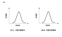
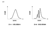
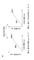
- FIG. It is a figure which shows the radiation angle characteristic of the laser beam of the semiconductor laser apparatus which the transverse mode is normal. It is a figure which shows the radiation angle characteristic of the laser beam of the semiconductor laser apparatus which the transverse mode is abnormal. It is a figure which shows the total light output characteristic and the horizontal mode output characteristic of the laser beam of the semiconductor laser apparatus which the horizontal mode is normal.
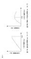
- FIG. It is a figure which shows the total light output characteristic and the horizontal mode output characteristic of the laser beam of the semiconductor laser apparatus which the lateral mode is abnormal. It is a flow figure explaining the procedure of the inspection method of the semiconductor laser apparatus by Embodiment 1.
- FIG. It is the schematic which shows the structure of the inspection apparatus of the semiconductor laser apparatus according to Embodiment 2 and the semiconductor laser apparatus which is an inspection target.
- FIG. 1 is a schematic view showing a configuration of an inspection device 11 of a semiconductor laser device according to the first embodiment and a semiconductor laser device 100 to be inspected.
- the inspection device 11 of the semiconductor laser device is shown in a block diagram, and the semiconductor laser device 100 is shown in a schematic side sectional view.
- FIG. 2 shows a top view of the semiconductor laser device 100, and the semiconductor laser device 100 of FIG. 1 is shown as a cross-sectional view at the position AA'of FIG.
- a semiconductor laser (also referred to as LD) 1 and an electric field absorption type modulator (also referred to as EAM) 2 are monolithically integrated, and the optical waveguides of both are coupled.
- the laser beam output by LD1 is introduced into EAM2 with low loss.
- a window structure 31 having a refractive index lower than that of EAM2 is formed on the output side of EAM2, that is, in the vicinity of the chip end surface (front end surface) on the EAM2 side.
- the laser beam output by the LD1 passes through the EAM2 and is radiated while diffusing into the window structure 31.
- a photodetector (also referred to as PD) 4 which is an optical monitor is formed in the vicinity of the window structure 31 so as to receive a part of the diffused light.
- Both EAM2 and PD4 absorb the incident light by applying a reverse bias voltage and output a photocurrent.
- the photocurrent output by EAM2 will be referred to as Iea
- the photocurrent output by PD4 will be referred to as Im.
- the inspection device 11 of the semiconductor laser device goes to the LD (semiconductor laser) power supply 5 for supplying the injection current to the LD1, the EAM (electric field absorption type modulator) power supply 6 for supplying the reverse bias voltage to the EAM2, and the PD4.
- a PD (photodetector) power supply 7 for supplying a reverse bias voltage is provided.
- the LD power supply 5 includes a current detector 51 that detects the LD injection current Iop, which is the current flowing through the LD 1, and the EAM power supply 6 includes an photocurrent detector 61 that detects Iea. Further, the PD power supply 7 includes an photocurrent detector 71 that detects Im. Needless to say, these current detector 51, photocurrent detector 61, and photocurrent detector 71 may be provided separately from their respective power supplies.
- the inspection device 11 of the semiconductor laser device further includes an inspection controller 10 that controls the LD power supply 5, the EAM power supply 6, and the PD power supply 7 to acquire Iop, Iea, and Im data.
- the photoelectric flow rate output by EAM2 and PD4 is designed to be proportional to the input optical power. Therefore, if the optical power incident on the EAM2 and PD4 increases linearly, the optical currents Iea and Im output by both will also increase linearly.
- EAM2 Since the optical waveguides of EAM2 and LD1 are continuously formed and they are coupled with low loss, EAM2 absorbs most of the laser light output by LD1. On the other hand, since the PD4 receives a part of the laser light diffused in the window structure 31, it absorbs only a part of the horizontal mode of the laser light output by the LD1.
- FIGS. 3A and 3B show the emission angles of the output laser light during low current drive and high current drive in the case of a semiconductor laser device in which the transverse mode does not fluctuate depending on the Iop and the transverse mode is normal.
- the transverse mode When the transverse mode is normal, the radiation angle does not fluctuate between low current drive and high current drive, and FFP does not fluctuate either.
- 4A and 4B show the emission angles of the output laser light during low current drive and high current drive in the case of a semiconductor laser device in which the transverse mode fluctuates depending on the Iop and the transverse mode is abnormal.
- the horizontal mode is abnormal, it is a single mode at the time of low current driving, but it becomes a multi-mode at the time of high current driving, the light emission pattern fluctuates from the time of low current driving, and the FFP fluctuates.
- Iea-I curve or total light output characteristic
- Im-I curve or Im-I curve, or Im-I curve, or
- Horizontal mode light output characteristics are shown respectively.
- the Iea-I curve and the Im-I curve of a semiconductor laser whose luminous efficiency is saturated in the high current region are shown as examples, but both are linear in the low current region and linear in the high current region. It is non-linear and has a similar waveform.
- FIGS. 6A and 6B show an example of the Iea-I curve and the Im-I curve when the transverse mode is abnormal. Since the EAM2 receives most of the light in the horizontal mode, the ratio of the light received by the EAM2 to the total laser output changes little even if the horizontal mode fluctuates. On the other hand, since the photodetector PD4 receives only a part of the horizontal mode, when the horizontal mode fluctuates, the ratio of the photodetector PD4 receiving light to the total laser output fluctuates greatly. Therefore, different waveforms can be obtained for the Iea-I curve and the Im-I curve. Similar to FIGS. 5A and 5B, FIGS.
- FIG. 6A and 6B show the Iea-I curve and the Im-I curve in the case of a semiconductor laser in which the luminous efficiency of LD1 is saturated in a high current region.
- the Iea-I curve shown in FIG. 6A has a non-linear waveform only in the high current region as in FIG. 5A, but the Im-I curve shown in FIG. 6B has non-linearity in a smaller current region, and both have different waveforms. ing.
- FIG. 7 is a flow chart collectively showing the inspection method of the semiconductor laser device according to the first embodiment.
- the semiconductor laser device 100 shown in FIGS. 1 and 2 is the inspection target.
- the inspection controller 10 controls the LD power supply 5 to measure the photocurrent Im, which is the output of the PD4, while changing the injection current Iop of the LD, and obtains the Im-I curve, which is the transverse mode light output characteristic.
- Acquire step ST1
- the reverse bias voltage is not applied to the EAM2, or the reverse bias voltage is applied to the EAM2 so as not to absorb the laser beam significantly.
- the inspection controller 10 controls the EAM power supply 6 to apply a reverse bias voltage to the EAM 2 to the extent that it absorbs light (step ST2).
- the inspection controller 10 measures the photocurrent Iea, which is the output of EAM2, while controlling the LD power supply 5 to change the injection current Iop of the LD, and the total optical output characteristics. Acquires the Iea-I curve which is (step ST3).
- the acquired horizontal mode light output characteristic and the total light output characteristic are compared to determine whether or not the LD of the semiconductor laser device to be inspected has a horizontal mode abnormality (step ST4).
- step ST2 and step ST3 may be performed before step ST1. In this case, when the step ST1 is executed, the EAM2 is kept in a state where the reverse bias voltage is not applied or the bias voltage is applied so as not to absorb the laser beam significantly so that the laser beam passes through the EAM2. Needless to say.
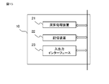
- Each of the above steps is actually a program stored in the storage device 22 in the inspection controller 10 including the arithmetic processing unit 21, the storage device 22, and the input / output interface 23, for example, as shown in FIG. Can be realized by the arithmetic processing unit 21 executing. That is, the inspection controller 10 transmits a control signal to each power source through the input / output interface 23, acquires data such as each current value, and determines the transverse mode abnormality.
- the inspection device of the semiconductor laser device shown in FIG. 1 it is possible to accurately determine whether or not LD1 of the semiconductor laser device 100 to be inspected has a transverse mode abnormality by the inspection method shown in FIG. ..
- the PD4 which is a light detector possessed by the semiconductor laser device 100, measures the intensity of a part of the laser light output by the semiconductor laser LD1 to acquire the transverse mode light output characteristic, and the semiconductor laser device 100
- the total light output characteristic corresponding to the output of all laser light is acquired by using the electric field absorption type modulator EAM2. Therefore, it is not necessary to use an additional photodetector as an inspection device.
- LD1 is a transverse mode normal element and integrates a semiconductor laser having an Iea-I curve
- a semiconductor laser having an Iea-I curve that is, a semiconductor laser having a non-linear characteristic even in a region other than the saturation region
- only the transverse mode optical output characteristic is used.
- FIG. 8 is a schematic view showing the configuration of the semiconductor laser device inspection device 11 according to the second embodiment and the semiconductor laser device 101 to be inspected.
- the configuration of the inspection device 11 of the semiconductor laser device is the same as that of the first embodiment.
- LD1 and EAM2 are monolithically integrated, and the optical waveguides of both are coupled with low loss.
- a window structure 32 having a refractive index lower than that of LD1 is formed in the vicinity of the chip end surface (rear end surface) on the LD1 side.
- the laser beam output by the LD1 is radiated while diffusing into the window structure 32.
- a photodetector PD4 is formed in the vicinity of the window structure 32 so as to receive a part of the diffused light.
- the EAM2 receives most of the laser beam output from the LD1 in the transverse mode, while the PD4 receives only a part of the transverse mode. Therefore, if both the Iea-I curve and the Im-I curve are measured in the same manner as in the first embodiment, and the semiconductor laser device having a large difference between the two is determined to be a transverse mode abnormality and removed, it depends on the Iop. It is possible to remove a semiconductor laser device in which the transverse mode fluctuates and the transverse mode is abnormal.
- the procedure in the inspection method of the semiconductor laser apparatus according to the second embodiment is the same as that in FIG. 7.
- the merit of the semiconductor laser device 101, which is the inspection target of the second embodiment, will be described with respect to the semiconductor laser device 100, which is the inspection target of the inspection device of the semiconductor laser device according to the first embodiment.
- the semiconductor laser device 100 which is the inspection target of the first embodiment, has a structure in which the PD4 receives the output light of the EAM2, there is a problem that the APC (Auto Power Control) control becomes complicated.
- the APC control is to give feedback to the injection current to the LD1 so that the photocurrent (that is, the amount of light received) output by the monitor is constant. By this control, it is possible to suppress the time-dependent change in the optical signal intensity output by the semiconductor laser LD1.
- the semiconductor laser device when the semiconductor laser device is incorporated in the optical communication system, the semiconductor laser device does not always output an optical signal, and the operation may be temporarily suspended depending on the timing.
- the optical current (light receiving amount) of the PD4 drops sharply in the semiconductor laser apparatus 100 to be inspected in the first embodiment. It is conceivable that the injection current into the LD1 rises sharply due to the APC control, causing the LD1 to fail. In order to avoid this, it is necessary to perform control so that not only EAM2 but also LD1 is stopped at the same time during the pause.
- the PD4 directly receives the output light of the LD1
- the amount of light received by the PD4 changes even if an electric signal for pausing is applied to the EAM2 side.
- the injection current into the LD1 does not change abruptly, and the above-mentioned problems do not occur. Therefore, simple APC control can be applied.
- both the semiconductor laser device 100 shown in the first embodiment and the semiconductor laser device 101 shown in the second embodiment the PD4 detects a part of the laser light of the spatial distribution generated by the transverse mode of the laser light output by the LD1. Therefore, the PD4 can detect the fluctuation of the horizontal mode. Therefore, both the semiconductor laser device 100 shown in the first embodiment and the semiconductor laser device 101 shown in the second embodiment are inspected by the inspection device 11 of the semiconductor laser device and the semiconductor laser device described in the first embodiment. It can be inspected by the method.
- Embodiment 3 In the third to fifth embodiments of the present embodiment, a specific method for determining a semiconductor laser device having an abnormal transverse mode will be described.
- 9A and 9B are diagrams for explaining the inspection method of the semiconductor laser apparatus according to the third embodiment.
- the Iea-I curve (FIG. 9A) and the Im-I curve (FIG. 9B) acquired when the transverse mode is unstable and the semiconductor laser apparatus is abnormal are shown as inspection targets.
- FIG. 9A in the Iea-I curve, which is the total light output characteristic, an extreme value due to saturation can be seen.
- the Im-I curve which is the horizontal mode optical output characteristic, a plurality of extreme values may be seen as shown in FIG. 9B due to the unstable horizontal mode.
- the transverse mode is stable, for example, as shown in FIG. 5B, the number of extreme values in the Im-I curve is the same as that in the Iea-I curve. Therefore, for each of the Iea-I curve and Im-I curve, the number of extrema is compared, and if they match, the transverse mode is considered to be stable, and if they do not match, the transverse mode is considered to be unstable.
- the extremum can be specified as the value at the position where the sign of the differential value of the characteristic curve is inverted.
- the Iea-I curve in FIG. 9A has an extremum number of 1, but the Im-I curve in FIG. 9B has an extremum number of 3, and they do not match. It can be determined that the semiconductor laser device having such characteristics is a semiconductor laser device having an abnormal transverse mode.
- Embodiment 4. 10A and 10B are diagrams for explaining the inspection method of the semiconductor laser apparatus according to the fourth embodiment.
- the Iea-I curve (Fig. 10A) which is the total light output characteristic
- the Im-I curve (Fig. 10B) which is the horizontal mode light output characteristic, acquired when the horizontal mode is an abnormal semiconductor laser device as inspection targets. Is shown.
- FIG. 10A in the Iea-I curve, an extreme value due to saturation is seen, and in the Im-I curve, the transverse mode becomes unstable, so that the injection corresponds to the extreme value of the Iea-I curve. Extreme values may be seen at injection currents Iops smaller than the current Iops.
- the extremum of the Im-I curve also appears at the same Iop position as the extremum of the Iea-I curve. Therefore, for each of the Iea-I curve and Im-I curve, the Iop at which the extremum appears is measured, and if they match, the transverse mode can be regarded as stable, and if they do not match, the transverse mode can be regarded as unstable. ..
- the Iop in which the extreme value appears in the Iea-I curve is Iop1
- the Iop in which the extreme value appears in the Im-I curve is Iop2.
- the transverse mode of the semiconductor laser device to be inspected is stable, and it can be judged as a non-defective product.
- Iop1 and Iop2 do not match, it can be determined that the semiconductor laser device to be inspected has a transverse mode abnormality.
- FIG. 11A shows the Iea-I curve, which is the total light output characteristic acquired when the horizontal mode is an unstable semiconductor laser device
- FIG. 11B shows the Im-I curve, which is the horizontal mode light output characteristic. Is shown.
- FIG. 11C shows the derivative value curve of the Iea-I curve
- FIG. 11D shows the derivative value curve of the Im-I curve
- FIG. 11E shows the product of the derivative value of the Iea-I curve and the derivative value of the Im-I curve. The value curve is shown.
- the product of the differential values of the Iea-I curve and the Im-I curve is obtained, and the symbol thereof is obtained in the region equal to or higher than the threshold current (Ith), which is the injection current at which LD1 starts laser oscillation.
- Ith the threshold current
- the product of the differential values always takes a positive value in the region above Ith.
- the transverse mode is unstable and the Im-I curve has a non-linear waveform different from the Iea-I curve as shown in Fig. 11B
- the product of the differential values in the region above Ith as shown in Fig. 11E. Is not always positive, and there is a region where it is negative.
- a semiconductor laser device having such characteristics can be determined to have a transverse mode abnormality.
- the Iea-I curve as in the fourth embodiment even when the number of extreme values differs between the Iea-I curve and the Im-I curve as in the third embodiment, the Iea-I curve as in the fourth embodiment and the Iea-I curve are used.
- the number of extreme values is the same for the Im-I curve, but even if the positions of the extreme values are different, there is an advantage that it can be determined as a transverse mode abnormality in either case.
- FIG. 12 is a schematic view showing the configuration of the semiconductor laser device inspection device 12 according to the sixth embodiment and the semiconductor laser device 102 to be inspected.
- the sixth embodiment is an embodiment in which the semiconductor laser device 102 not provided with a photodetector is targeted for inspection.
- the semiconductor laser (LD) 1 and the electric field absorption type modulator (EAM) 2 are monolithically integrated, and the optical waveguides of both are coupled.
- the semiconductor laser device 102 is not provided with a photodetector.
- the inspection device 12 of the semiconductor laser device is provided with a photodetector (PD) 40, and the PD 40 receives only a part of the spatial distribution of the laser light output by the semiconductor laser device 102, that is, a part of the transverse mode. Place in position.
- the PD 40 is controlled by a PD power source 70 equipped with an photocurrent detector 71.
- the photocurrent output by the PD40 behaves in the same manner as the photocurrent Im of the photodetector (PD) 4 described in the first embodiment and the third to fifth embodiments. Therefore, by comparing the photocurrents Iea of EAM2 and the photocurrents of PD40, the semiconductor laser device 102 having an abnormal transverse mode can be determined by the same method as described in the first embodiment and the third to fifth embodiments. Can be done.
- one photodetector is required as the inspection device 12 of the semiconductor laser device, but the semiconductor laser device 102 having the EAM 2 but not the photodetector is to be inspected, and the EAM 2 is used.
- the total light output characteristic can be obtained by measuring the light current of. Therefore, by comparing the total light output characteristic and the horizontal mode light output characteristic, it is possible to accurately determine whether or not the semiconductor laser device to be inspected has a horizontal mode abnormality.
- FIG. 13 is a schematic view showing the configuration of the semiconductor laser device inspection device 13 according to the seventh embodiment and the semiconductor laser device 103 to be inspected.
- the seventh embodiment is an embodiment in which a semiconductor laser device 103 having only a semiconductor laser (LD) 1 as a light emitting element, which does not have an electric field absorption type modulator (EAM) or a photodetector, is to be inspected. .. Since the inspection target is not provided with a photodetector, the inspection device 13 of the semiconductor laser device receives only a part of the spatial distribution of the laser light emitted from the front end surface of the semiconductor laser device 103, that is, a part of the transverse mode.
- LD semiconductor laser
- EAM electric field absorption type modulator
- the first photodetector (first PD) 41 arranged at the position is provided. Further, a first PD power supply 73 is provided with a photocurrent detector 74 by applying a reverse bias voltage to the first PD 41. Further, since the inspection target is not provided with EAM, the second photodetector (the second photodetector) arranged in the inspection device 13 of the semiconductor laser device at a position where all the laser light emitted from the rear end surface of the semiconductor laser device 103 is received. (2) PD) 42 is provided. Further, a reverse bias voltage is applied to the second PD 42, the photocurrent detector 76 is provided, and the second PD power supply 75 is provided.
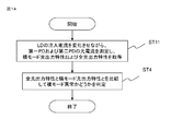
- the photocurrent output by the PD41 behaves in the same manner as the photocurrent Im of the PD4 described in the first embodiment and the third to fifth embodiments. Further, the photocurrent output by the PD42 behaves in the same manner as the photocurrent Iea of EAM2 described in the first embodiment and the third to fifth embodiments. Therefore, as shown in the flow chart of FIG. 14, by measuring the photocurrents of the first PD41 and the second PD42 while controlling the LD power supply 5 by the inspection controller 10 to change the injection current Iop into the LD1. , Transverse mode light output characteristics and total light output characteristics can be obtained (step ST11). Further, by the same method as described in the first embodiment and the third to fifth embodiments, the total light output characteristic and the transverse mode optical output characteristic are compared to determine whether or not the transverse mode is abnormal (step ST4). be able to.
- the seventh embodiment two photodetectors are required as the inspection device 13 of the semiconductor laser device, but the total light output of the semiconductor laser device 103 having neither EAM nor a photodetector as an inspection target.
Landscapes
- Physics & Mathematics (AREA)
- Condensed Matter Physics & Semiconductors (AREA)
- General Physics & Mathematics (AREA)
- Electromagnetism (AREA)
- Optics & Photonics (AREA)
- Semiconductor Lasers (AREA)
Priority Applications (4)
| Application Number | Priority Date | Filing Date | Title |
|---|---|---|---|
| US17/755,308 US20220376465A1 (en) | 2020-01-09 | 2020-01-09 | Inspection method for semiconductor laser device and inspection device for semiconductor laser device |
| CN202080091181.7A CN114902506B (zh) | 2020-01-09 | 2020-01-09 | 半导体激光装置的检查方法、以及半导体激光装置的检查装置 |
| JP2021569669A JP7271726B2 (ja) | 2020-01-09 | 2020-01-09 | 半導体レーザ装置の検査方法、および半導体レーザ装置の検査装置 |
| PCT/JP2020/000477 WO2021140618A1 (ja) | 2020-01-09 | 2020-01-09 | 半導体レーザ装置の検査方法、および半導体レーザ装置の検査装置 |
Applications Claiming Priority (1)
| Application Number | Priority Date | Filing Date | Title |
|---|---|---|---|
| PCT/JP2020/000477 WO2021140618A1 (ja) | 2020-01-09 | 2020-01-09 | 半導体レーザ装置の検査方法、および半導体レーザ装置の検査装置 |
Publications (1)
| Publication Number | Publication Date |
|---|---|
| WO2021140618A1 true WO2021140618A1 (ja) | 2021-07-15 |
Family
ID=76787796
Family Applications (1)
| Application Number | Title | Priority Date | Filing Date |
|---|---|---|---|
| PCT/JP2020/000477 Ceased WO2021140618A1 (ja) | 2020-01-09 | 2020-01-09 | 半導体レーザ装置の検査方法、および半導体レーザ装置の検査装置 |
Country Status (4)
| Country | Link |
|---|---|
| US (1) | US20220376465A1 (https=) |
| JP (1) | JP7271726B2 (https=) |
| CN (1) | CN114902506B (https=) |
| WO (1) | WO2021140618A1 (https=) |
Families Citing this family (1)
| Publication number | Priority date | Publication date | Assignee | Title |
|---|---|---|---|---|
| CN121208578B (zh) * | 2025-11-28 | 2026-04-24 | 度亘核芯光电技术(苏州)股份有限公司 | 单模半导体激光器失效评估方法、装置及电子设备 |
Citations (9)
| Publication number | Priority date | Publication date | Assignee | Title |
|---|---|---|---|---|
| US4795976A (en) * | 1987-01-15 | 1989-01-03 | American Telephone And Telegraph Company At&T Bell Laboratories | Apparatus and derivative technique for testing devices |
| JPH04259279A (ja) * | 1991-02-14 | 1992-09-14 | Toshiba Corp | 半導体レーザのキンク測定装置 |
| JPH07307516A (ja) * | 1994-05-13 | 1995-11-21 | Kokusai Denshin Denwa Co Ltd <Kdd> | 波長可変半導体レーザ装置 |
| US20030137023A1 (en) * | 2002-01-09 | 2003-07-24 | Bernhard Stegmuller | Optoelectronic device, and method for producing an optoelectronic device |
| JP2005142324A (ja) * | 2003-11-06 | 2005-06-02 | Sanyo Electric Co Ltd | 半導体レーザー測定装置 |
| JP2006294999A (ja) * | 2005-04-13 | 2006-10-26 | Sharp Corp | 半導体レーザ素子の光学特性生成装置および光学特性生成方法 |
| JP2007207999A (ja) * | 2006-02-01 | 2007-08-16 | Daitron Technology Co Ltd | 半導体レーザ素子の入出力特性検出方法とその装置 |
| WO2012085596A1 (en) * | 2010-12-23 | 2012-06-28 | Oclaro Technology Ltd | A laser-locker assembly |
| JP2019057541A (ja) * | 2017-09-19 | 2019-04-11 | 日本電信電話株式会社 | 半導体光集積素子 |
Family Cites Families (8)
| Publication number | Priority date | Publication date | Assignee | Title |
|---|---|---|---|---|
| JP3323725B2 (ja) * | 1995-12-08 | 2002-09-09 | キヤノン株式会社 | 偏波変調レーザ、その駆動方法及びそれを用いた光通信システム |
| US6222202B1 (en) * | 1998-10-06 | 2001-04-24 | Agilent Technologies, Inc. | System and method for the monolithic integration of a light emitting device and a photodetector for low bias voltage operation |
| US7120183B2 (en) * | 2001-07-11 | 2006-10-10 | Optium Corporation | Electro-absorption modulated laser with high operating temperature tolerance |
| JP5043880B2 (ja) * | 2009-03-31 | 2012-10-10 | 日本オクラロ株式会社 | 半導体素子及びその製造方法 |
| JP2011187580A (ja) * | 2010-03-05 | 2011-09-22 | Sony Corp | 自励発振型半導体レーザ素子及びその駆動方法 |
| JP2012033738A (ja) * | 2010-07-30 | 2012-02-16 | Ricoh Co Ltd | 半導体レーザ駆動装置及びその半導体レーザ駆動装置を備えた画像形成装置 |
| JP2012141335A (ja) * | 2010-12-28 | 2012-07-26 | Mitsubishi Electric Corp | 非冷却光半導体装置 |
| JP2015026645A (ja) * | 2013-07-24 | 2015-02-05 | キヤノン株式会社 | 面発光レーザおよび光干渉断層計 |
-
2020
- 2020-01-09 JP JP2021569669A patent/JP7271726B2/ja active Active
- 2020-01-09 WO PCT/JP2020/000477 patent/WO2021140618A1/ja not_active Ceased
- 2020-01-09 US US17/755,308 patent/US20220376465A1/en active Pending
- 2020-01-09 CN CN202080091181.7A patent/CN114902506B/zh active Active
Patent Citations (9)
| Publication number | Priority date | Publication date | Assignee | Title |
|---|---|---|---|---|
| US4795976A (en) * | 1987-01-15 | 1989-01-03 | American Telephone And Telegraph Company At&T Bell Laboratories | Apparatus and derivative technique for testing devices |
| JPH04259279A (ja) * | 1991-02-14 | 1992-09-14 | Toshiba Corp | 半導体レーザのキンク測定装置 |
| JPH07307516A (ja) * | 1994-05-13 | 1995-11-21 | Kokusai Denshin Denwa Co Ltd <Kdd> | 波長可変半導体レーザ装置 |
| US20030137023A1 (en) * | 2002-01-09 | 2003-07-24 | Bernhard Stegmuller | Optoelectronic device, and method for producing an optoelectronic device |
| JP2005142324A (ja) * | 2003-11-06 | 2005-06-02 | Sanyo Electric Co Ltd | 半導体レーザー測定装置 |
| JP2006294999A (ja) * | 2005-04-13 | 2006-10-26 | Sharp Corp | 半導体レーザ素子の光学特性生成装置および光学特性生成方法 |
| JP2007207999A (ja) * | 2006-02-01 | 2007-08-16 | Daitron Technology Co Ltd | 半導体レーザ素子の入出力特性検出方法とその装置 |
| WO2012085596A1 (en) * | 2010-12-23 | 2012-06-28 | Oclaro Technology Ltd | A laser-locker assembly |
| JP2019057541A (ja) * | 2017-09-19 | 2019-04-11 | 日本電信電話株式会社 | 半導体光集積素子 |
Also Published As
| Publication number | Publication date |
|---|---|
| CN114902506B (zh) | 2025-02-25 |
| JP7271726B2 (ja) | 2023-05-11 |
| CN114902506A (zh) | 2022-08-12 |
| US20220376465A1 (en) | 2022-11-24 |
| JPWO2021140618A1 (https=) | 2021-07-15 |
Similar Documents
| Publication | Publication Date | Title |
|---|---|---|
| US7036979B2 (en) | Photothermal transducing spectroscopic analyzer | |
| US9685757B2 (en) | System, method and fixture for performing both optical power and wavelength measurements of light emitted from a laser diode | |
| US20040090659A1 (en) | Method of tuning wavelength tunable electro-absorption modulators | |
| US10658809B2 (en) | Optical power monitoring device, laser device, and laser system | |
| US8665919B2 (en) | Semiconductor laser module | |
| US6895147B2 (en) | Laser power monitoring tap | |
| JP2006013252A (ja) | レーザダイオードの制御方法、制御回路、および光送信器 | |
| JP2011238698A (ja) | レーザモジュール | |
| CN105227243A (zh) | 一种控制消光比的电路、芯片和光模块 | |
| US9287988B2 (en) | Optical communication techniques | |
| US11607746B2 (en) | Laser device and laser processing device using same | |
| CN114323586A (zh) | 一种基于双通道检测的波导损耗测量方法 | |
| WO2021140618A1 (ja) | 半導体レーザ装置の検査方法、および半導体レーザ装置の検査装置 | |
| US20140036258A1 (en) | Optical transmission line connection system and optical transmission line connection method | |
| US9548819B2 (en) | Method to control optical receiver implemented with semiconductor optical amplifier and method to control optical communication | |
| US11435537B2 (en) | Method and apparatus for measuring optical characteristics of optical modulation device, and non-transitory computer-readable medium | |
| JP3853411B2 (ja) | 半導体レーザモジュール及び半導体レーザモジュールを用いた光通信システム | |
| JP2020027844A (ja) | 半導体レーザ装置 | |
| US7088752B2 (en) | Slope efficiency measurement apparatus for a laser device and method therefor | |
| TWI814190B (zh) | 頻率調變連續波光學雷達裝置 | |
| US20070121683A1 (en) | Direct control of extinction ratio and optical modulation amplitude for fiber transmitters | |
| JP5063300B2 (ja) | レーザモジュール | |
| US20060062259A1 (en) | Optical wavelength control system and related method of assembly | |
| CN112229518A (zh) | 一种芯片吸收谱的测量方法、装置、设备及存储介质 | |
| JP2012156430A (ja) | 光半導体モジュール |
Legal Events
| Date | Code | Title | Description |
|---|---|---|---|
| 121 | Ep: the epo has been informed by wipo that ep was designated in this application |
Ref document number: 20911492 Country of ref document: EP Kind code of ref document: A1 |
|
| ENP | Entry into the national phase |
Ref document number: 2021569669 Country of ref document: JP Kind code of ref document: A |
|
| NENP | Non-entry into the national phase |
Ref country code: DE |
|
| 122 | Ep: pct application non-entry in european phase |
Ref document number: 20911492 Country of ref document: EP Kind code of ref document: A1 |
|
| WWG | Wipo information: grant in national office |
Ref document number: 202080091181.7 Country of ref document: CN |