WO2021125164A1 - 気密コネクタおよびその製造方法 - Google Patents
気密コネクタおよびその製造方法 Download PDFInfo
- Publication number
- WO2021125164A1 WO2021125164A1 PCT/JP2020/046736 JP2020046736W WO2021125164A1 WO 2021125164 A1 WO2021125164 A1 WO 2021125164A1 JP 2020046736 W JP2020046736 W JP 2020046736W WO 2021125164 A1 WO2021125164 A1 WO 2021125164A1
- Authority
- WO
- WIPO (PCT)
- Prior art keywords
- space
- connector
- skin layer
- skinless
- connector base
- Prior art date
- Legal status (The legal status is an assumption and is not a legal conclusion. Google has not performed a legal analysis and makes no representation as to the accuracy of the status listed.)
- Ceased
Links
Images




Classifications
-
- H—ELECTRICITY
- H01—ELECTRIC ELEMENTS
- H01R—ELECTRICALLY-CONDUCTIVE CONNECTIONS; STRUCTURAL ASSOCIATIONS OF A PLURALITY OF MUTUALLY-INSULATED ELECTRICAL CONNECTING ELEMENTS; COUPLING DEVICES; CURRENT COLLECTORS
- H01R43/00—Apparatus or processes specially adapted for manufacturing, assembling, maintaining, or repairing of line connectors or current collectors or for joining electric conductors
-
- H—ELECTRICITY
- H01—ELECTRIC ELEMENTS
- H01R—ELECTRICALLY-CONDUCTIVE CONNECTIONS; STRUCTURAL ASSOCIATIONS OF A PLURALITY OF MUTUALLY-INSULATED ELECTRICAL CONNECTING ELEMENTS; COUPLING DEVICES; CURRENT COLLECTORS
- H01R9/00—Structural associations of a plurality of mutually-insulated electrical connecting elements, e.g. terminal strips or terminal blocks; Terminals or binding posts mounted upon a base or in a case; Bases therefor
- H01R9/16—Fastening of connecting parts to base or case; Insulating connecting parts from base or case
Definitions
- the present invention relates to an airtight connector that makes an electrical connection via a conductive terminal while maintaining airtightness, and a method for manufacturing the same.
- the performance of small electronic components is greatly affected by the humidity and the viscosity of the enclosed gas. Therefore, in order to prevent corrosion of internal circuits due to humidity and malfunction due to changes in the viscosity of the gas, it is sealed and sealed with a vacuum or an inert gas. Has been done.
- a closed container is used, and in order to introduce a power source without impairing the airtightness of the closed container and to extract internal sensor signals, etc.
- An airtight (hermetic) connector with airtightness is used.
- a through hole is provided in a ceramic plate for blocking the internal atmosphere and the external atmosphere, an insulating substrate such as a glass epoxy plate, or a metal plate.
- an insulating substrate such as a glass epoxy plate, or a metal plate.
- a metal pin for electrical connection is inserted into this through hole, and the gap is closed by glass sealing, silver brazing, soldering, or the like for joining.
- thermoplastic synthetic resins with excellent corrosion resistance and insulation properties which are suitable for injection molding, are widely used not only for substrate mounting but also for component cases.
- the liquid crystal polymer (LCP) resin has many advantages such as excellent fluidity during molding, high heat resistance, and excellent chemical resistance.
- the liquid crystal polymer (LCP) resin has drawbacks such as anisotropy of the molded product and low weld strength. In order to improve this, modification is performed by filling glass fibers and the like. In addition, in order to improve elasticity and strength, reinforcement with inorganic fillers such as glass beads and calcium pyrophosphate is also performed.
- the airtight connector according to the first embodiment of the present invention maintains the airtightness between the first space and the second space, and the first conductor and the second space in the first space. It is an airtight connector for electrically connecting the second conductor inside, and is provided with a hole for communicating the first space and the second space, and divides the two spaces by a portion other than the hole. It has a connector base of an insulator having a partition, and the first surface of the connector base has a first skinned portion and a first unskinned portion, and the first unskinned portion is roughened. It is characterized by having a first conductive portion, for example, a plated portion, which is formed as an integral member that is in close contact with the surface and covers the holes.
- the conductive portion that closes the hole maintains the airtightness between the first space and the second space, and electrically connects the first conductor and the second conductor. It is possible to obtain good conductivity and high airtightness. It is also possible to form a conductive portion as a circuit wiring and mount an electronic component on the conductive portion.
- the second surface of the connector base located on a surface different from the first surface, for example, the opposite surface is It has a second skinned portion and a second unskinned portion, and is formed so as to be in close contact with the roughened surface of the second skinless portion and to be electrically connected to the first conductive portion. It is characterized by having a second conductive portion.
- the airtight connector according to the third embodiment of the present invention maintains the airtightness between the first space and the second space, and the first conductor and the second space in the first space. It is an airtight connector for electrically connecting the second conductor inside, and is provided with a hole for communicating the first space and the second space, and divides the two spaces by a portion other than the hole. It has a connector base of an insulator having a partition, the connector base is an injection-molded product of synthetic resin, and the first surface of the connector base has a first skinned portion and a first unskinned portion. The surface of the skinless portion has a recess, is formed so as to enter the recess, and has a conductive portion formed as an integral member covering the hole. With such a configuration, high airtightness and high adhesion that can withstand the mounting of electronic components can be obtained due to the high adhesion of the conductive portion to the skinless portion.
- the method for manufacturing an airtight connector according to the first embodiment of the present invention maintains airtightness between the first space and the second space, and maintains the airtightness between the first conductor and the first space in the first space.
- a first skin layer removing step for forming a skinless portion a first conductive portion forming step for forming a first conductive portion on the surface of the first skinless portion and the molded body, and a molded body for removing the molded body. It is characterized by having a removal step. With such a configuration, the conductive portion is formed in the skinless portion without masking, and the circuit wiring can be performed by selectively forming the conductive portion in the airtight connector.
- the method for manufacturing an airtight connector according to the second embodiment of the present invention includes the manufacturing method of (4) and a first roughening step of further roughening the first skinless portion.
- the first conductive portion forming step the roughened first skinless portion and the first conductive portion are formed on the surface of the molded body, and the roughened first skin layer is formed.
- the skin layer was removed by a second skin layer removing step of selectively removing the skin layer on a part of the surface different from the surface from which the skin layer was removed by the removing step, and a second skin layer removing step.
- the second roughening step of applying the roughening treatment to the second skinless portion, and the second roughened portion roughened by the second roughening step are provided with the first conductive portion.
- circuit wiring for mounting electronic components is provided not only on the upper surface side of the connector base but also on the lower surface side, for example, while realizing high airtightness in the airtight connector without masking. Can be formed.
- the method for manufacturing an airtight connector according to the first embodiment of the present invention maintains airtightness between the first space and the second space, and maintains the airtightness between the first conductor and the first space in the first space.
- the skin layer on a part of the surface of the connector base is selectively removed by a connector base forming step of forming the connector base having the above by injection molding of synthetic resin, a hole closing step of closing the holes with a molded body, and a laser processing process.
- it is characterized by including a skinless portion, a conductive portion forming step of forming a conductive portion on the surface of the molded body, and a molded body removing step of removing the molded body.
- FIG. 1 It is the schematic sectional drawing which shows the structural example of the airtight connector to which this invention is applied.
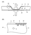
- (A) is a schematic cross-sectional view showing the configuration of an airtight connector according to an embodiment of the present invention, and (B) is a partially enlarged view thereof.
- (A) is a cross-sectional view showing a schematic configuration of a part of the airtight connector of the embodiment shown in FIG. 2, (B) a bottom view showing the schematic configuration, and (C) a side view showing the schematic configuration.
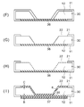
- It is the schematic cross-sectional view which shows the steps (F)-(I) of the manufacturing method of the airtight connector of the structure shown in FIG.
- FIG. 1 is a schematic cross-sectional view showing an example of an airtight connector to which the present invention is applied.
- the connector base 1 of an insulator is formed of, for example, a polyester-based liquid crystal polymer (LCP), and has a partition wall portion 4 that separates a first space 2 and a second space 3.
- LCP polyester-based liquid crystal polymer
- an appropriate filler can be added in order to improve the characteristics of the liquid crystal polymer (LCP).
- one space is, for example, a vacuum, pressure, liquid, gas environment, etc.
- the other space is, for example, an atmospheric atmosphere in which electronic components are stored.
- Electronic components may also be mounted in spaces such as vacuum, pressure, liquid, and gas environments.
- Airtight connectors are used in many industrial fields such as air conditioner compressors, gas sensors, flow rate sensors, and medical sensors, as well as aviation, space, defense, and security.
- the outer shape of the connector base 1 has a shape such as a substantially cylindrical shape or a substantially rectangular parallelepiped, depending on the use of these airtight connectors.
- the partition wall portion 4 is provided with a hole 5, and a conductive plated portion 6 such as copper having a thickness of about 25 ⁇ m is formed to cover the hole 5 and its periphery. In this example, the plated portion 6 is formed so as to cover the hole 5 and its peripheral portion.
- Pins 7 and 8 are members for electrical connection, such as pure copper, brass, phosphor bronze, etc., on which the surface of the base is gold-plated, tin-plated, or the like. Brazing is performed by soldering, silver brazing, gold-tin (AuSn) bonding by radio frequency induction heating (IH), or the like. If the LCP material leaks, epoxy resin, epoxy or acrylic resin impregnated sealing portions 9 and 10 may be provided.
- Such an airtight connector has a structure in which the airtightness is maintained and electrical connection is made by the plated portion 6.
- the plated portion 6 is formed so as to cover the hole 5 and its periphery, the contact area between the partition wall portion 4 and the plated portion 6 becomes large, so that the plated portion is formed when a force is applied to the pins 7 and 8. 6 is less likely to be peeled off from the partition wall portion 4, and the breaking strength of the airtight connector is improved.
- the plated portion 6 is an integral or single member with respect to the entire portion that is in close contact with the partition wall portion 4 and covers the hole 5. It should be noted that even when a plated portion having an increased thickness is formed by stacking electroless plating and electroplating, it is an integral or single member.
- the connector base 20 is an injection molded product of a synthetic resin, for example, LCP (liquid crystal polymer), and has a structure composed of a skin layer 11 on the surface and a core layer 12 on the inside.
- LCP liquid crystal polymer
- the mold temperature, holding pressure, and resin temperature are related to the formation of the skin layer, and it is necessary to stabilize the formation of the skin layer in order to reduce the molding compression and improve the dimensional accuracy of the molded product. Will be done.
- the skin layer portion is destroyed and the conductor portion is peeled off from the substrate.
- the actual thickness of the skin layer 11 varies depending on the injection conditions and is about 0.1 to 0.3 mm, but in FIG. 2 (A), it is schematically irrespective of the actual ratio with the thickness of the core layer. Shown.
- a plated portion 6 is formed on the upper surface side of the connector base 20 where there is no skin layer 11.
- the portion without the plating portion 6 is the skin portion 21 with the skin layer 11, and below the portion with the plating layer 6, there is no skin layer and the core layer 12 is not exposed. It is a skin portion 22.
- the surface of the core layer 12 of the non-skinned portion 22 is a rough surface with irregularities, and the adhesion to the plated portion 6 is high, so that leakage can be reliably prevented.
- a rough surface having irregularities is indicated by a broken line.
- the plated portion 6 is an integral or single member with respect to the entire portion that is in close contact with the roughened core layer 12 and covers the hole 5. It should be noted that even when a plated portion having an increased thickness is formed by stacking electroless plating and electroplating, it is an integral or single member. Also in the skinless portion 22 on the lower surface side of the connector base portion 20, the plated portion 26 is in close contact with the roughened core layer 12 and is electrically connected to the plated portion 6. Since the plated portions 6 and 26 are formed on the roughened core layer 12, the plating material enters the unevenness thereof to increase the adhesive strength, which is sufficient for mounting electronic components on the plated portions 6 and 26. Strength can be obtained.
- the airtight connector according to the present embodiment has a feature that the connector base 20 is covered with the skin layer 11 or the plated portions 6 and 26, so that the gas barrier property is high. Further, the skinned portion 21 in which the plated portions 6 and 26 are not formed has high mechanical strength because the skin layer is left.
- FIG. 2 (B) is an enlarged view of a part 29 in FIG. 2 (A).
- the core layer 12 contains a large number of additives 15 which are injection-molded together with the liquid crystal polymer resin. In the figure, only one is illustrated.
- the plated portion 6 is formed by inserting metal into the recess.
- FIG. 3 is a diagram schematically showing a connector base in one embodiment of an airtight connector according to the present invention.
- the connector base 30 is formed of, for example, an LDS material for manufacturing an injection molded circuit component (MID) by LDS (Laser Direct Structuring), and in this example, a liquid crystal polymer (LCP) resin is used. ..
- acrylonitrile butadiene (ABS) resin polycarbonate (PC) resin, PC / ABS resin, polycarbonate (PC) + polyethylene terephthalate (PET) resin, polyphthalamide (PPA) resin, polyamide / polyphthalamide ( Thermoplastics such as PA / PPA) resin, polybutylene terephthalate (PBT) resin, cycloolefin polymer (COP) resin, polyphenylene ether (PPE) resin, polyetherimide (PEI) resin, polyether ether ketone (PEEK) resin, etc. , Thermocurable resins such as phenol and epoxy can also be used.
- the material of the synthetic resin molded product other than the LDS molding material may be either a thermoplastic resin or a thermocurable resin material as long as it is a synthetic resin capable of firmly adhering a metal thin film. Considering that it will be subjected to severe treatment such as soldering later, a resin having high heat resistance and excellent mechanical strength is desirable, and an injection-moldable thermoplastic resin is preferable from the viewpoint of mass productivity.
- examples include aromatic polyesters, polyamides, polyacetals, polycarbonates, polyallylensulfides, polysulfones, polyphenylene oxides, polyimides, polyetherketones, polyarylates and compositions thereof, with particular high melting point, high strength and high strength.
- liquid crystal polymers for example, liquid liquid polyester, polyesteramide
- polyarylene sulfide are particularly suitable, but are not limited thereto.
- an appropriate substance such as an easily etchable substance may be added to the material as needed.
- a plated portion 6 is formed on the skinless portion 22 on the upper surface of the connector base portion 30 as in the connector base portion 20 in FIG. 2, and the holes 5 are formed by the plated portions 6. Is blocked.
- a skinned portion 21 and a skinless portion 22 are also formed on the lower surface of the connector base portion 30, and a plated portion 36 is formed on the roughened surface of the core layer 12 of the skinless portion 22.
- the plating portion 36 is electrically connected to the plating portion 6.
- the plating portion 37 formed on the plating portion 36 is also electrically connected to the plating portion 36 and the plating portion 6.
- the plated portions 6, 36, and 37 form an integral plated portion.
- FIG. 3B shows the lower surface of the connector base 30, and the plated portion 37 forms the circuit pattern of the plated portions 37A, 37B, and 37C.
- the plated portion 37A is a portion corresponding to the plated portion that closes the hole 5 in FIG. 2, the plated portion 37B is the circuit wiring electrically connected to the plated portion 37A, and the plated portion 37C is electrically connected to the plated portion 37A.
- FIG. 3C shows the side surface of the connector base portion 30, and the plated portion 37D formed on the side surface is electrically connected to the plated portion 37A via the plated portion 37B. In this way, circuit wiring can be formed on the upper surface, lower surface, and side surface of the connector base 30, and a small electronic component can be mounted on the circuit wiring.
- a synthetic resin such as LCP (liquid crystal polymer), PPA, PA, or thermosetting resin is injection-molded together with an additive to form a connector base 30 having holes 5.
- LCP liquid crystal polymer
- the connector base 30 formed by injection molding a liquid crystal polymer (LCP) resin has a skin layer 11 on the outside and a core layer 12 on the inside.
- the material of the connector base 30 is preferably an aromatic liquid crystal polymer, polysulfone, polyetherpolysulfone, polyarylsulfone, polyetherimide, polyester, acrylonitrile-butadiene-styrene copolymer resin, polyamide, modified polyphenylene oxide resin, norbornene resin. , Phenolic resin, epoxy resin, polyphenylene sulfide resin (PPS) resin, polybutylene terephthalate (PBT) resin and the like.
- PPS polyphenylene sulfide resin
- PBT polybutylene terephthalate
- a polyester-based liquid crystal polymer having heat resistance and a coefficient of thermal expansion close to that of a metal under a wide temperature condition, having elasticity equivalent to that of a metal film, and having excellent properties equivalent to those of a metal film in a thermal cycle test.
- the connector base 30 includes glass beads, glass balloons, glass powder, periodic table group II elements and their components in order to improve the anisotropy and low weld strength of the molded product, or to improve elasticity and strength.
- One or more fine powders selected from the group consisting of oxides, sulfates, phosphates, silicates, carbonates, or aluminum, silicon, tin, lead, antimony, bismuth elements and their oxides. It is injection-molded as an additive of.
- Oxides of elements of Group II of the periodic table are compounds such as magnesium oxide, calcium oxide, barium oxide, zinc oxide, etc.
- phosphates are magnesium phosphate, calcium phosphate, barium phosphate, zinc phosphate, etc.
- sulfate is a compound such as magnesium sulfate, calcium sulfate, barium sulfate, etc.
- silicate is magnesium silicate, calcium silicate, aluminum silicate, kaolin, talc. , Clay, diatomaceous earth, wollastonite and the like
- the carbonate is a compound such as calcium carbonate, magnesium carbonate, barium carbonate and zinc carbonate. Phosphate is particularly suitable.
- amphoteric metal elements such as zinc, aluminum, silicon, tin, lead, antimony, and bismuth, or oxides of the elements is also preferable, and zinc, in particular, zinc.
- Amphoteric metal elements such as aluminum, tin and lead and oxides thereof are preferable.
- the particle size of these fine powdery inorganic fillers or additives is preferably in the range of an average particle size of 0.01 to 100 ⁇ m, preferably 0.1 to 30 ⁇ m, and more preferably 0.5 to 10 ⁇ m.
- an organic material such as butadiene may be used as an additive for injection molding.
- the total amount of the additives may be, for example, about 25% by weight to about 55% by weight of the polymer composition.
- the particle size of these fine powdery inorganic fillers is preferably in the range of an average particle size of 0.01 to 100 ⁇ m, preferably 0.1 to 30 ⁇ m, and more preferably 0.5 to 10 ⁇ m.
- step (B) the lower side surface inside the hole 5 of the connector base 30 is roughened by etching.
- the molded body 40 is formed by using an acrylonitrile-butadiene-styrene (ABS) resin, a biodegradable resin, or the like so as to close the pores 5.
- ABS acrylonitrile-butadiene-styrene
- the skin layer 11 of the portion corresponding to the hole on the lower surface of the connector base 30 and its periphery is removed by laser processing.
- the laser processing process is a process of irradiating the surface of the skin layer 11 with a laser beam to remove the skin layer 11 in that portion and selectively etch the skin layer 11.
- a skin layer having a line width of 0.126 mm and an interval of 0.126 mm is removed with a laser output of 3.5 W, a frequency of 200 kHz, and an etching rate of 3 m / s.
- the skinless portion 22 is formed.
- the core layer 12 is exposed.
- the skinned portion 21 and the unskinned portion 22 are formed on the lower surface of the connector base portion 30.
- the laser beam to irradiate the skin layer 21 is a YAG laser, a carbon dioxide gas laser, or the like, and a preset circuit pattern is selectively irradiated by a laser marker having a scanning mechanism in the XY directions controlled by a computer.
- a laser marker having a scanning mechanism in the XY directions controlled by a computer.
- the laser beam is guided in a three-dimensional direction by an optical fiber, a prism, etc., and a predetermined area is accurately irradiated three-dimensionally by computer control. Can be done.
- Lasers can be from UV lasers to CO2 lasers, for example, UV lasers with a wavelength of 355 nm, green lasers with a wavelength of 532 nm, hybrid lasers with a wavelength of 1064 nm, YVO4 lasers, YAG lasers, fiber lasers with a wavelength of 1090 nm, and CO2 lasers with a wavelength of 10600 nm. ..
- UV lasers are characterized by high absorption rate and low thermal stress regardless of the material. Since the wavelength of the green laser is short, the energy is high and the absorption rate for substances is high.
- Targets YVO4 lasers that can perform high-quality and delicate processing with high-peak power short-pulse lasers, fiber lasers that apply heat with long-pulse lasers and are suitable for deep digging, and YAG lasers that are inferior in quality but generate a large amount of heat. It can be used properly according to the object and purpose.
- the CO2 laser is often used for marking on paper, resin, glass, and ceramic, and has a wavelength that is absorbed by a transparent material, and is also used for marking on a film. By realizing high output, it can also be used for gate cutting of molded products and cutting of PET sheets.
- these lasers are used under appropriate conditions such as laser power, scan speed, frequency, number of prints, print position and the like.
- energy may be selected condition in accordance with the wavelength of 0.1W / mm 2 ⁇ 1W / mm 2 and a laser.
- the surface of the connector base 30 is irradiated with laser light whose output and laser spot diameter are appropriately adjusted, and the skin layer 11 in this portion is selectively removed.
- the spot diameter of the laser used here and the width of the skin layer 11 to be removed are particularly important, and if the width to be removed is too narrow, a problem of short-circuiting of the conductive circuit portion due to etching in the next step occurs, which is not preferable. Therefore, it is preferable that the width of the skin layer to be removed is wide as long as it does not interfere with the circuit formation.
- the skin layer is removed with a width wider than the spot diameter due to the high energy density, but it is impossible to remove a skin layer with a sufficient width with a single irradiation. Therefore, the number of times of irradiation becomes too large and the laser irradiation time becomes long, so that the productivity is deteriorated and it is uneconomical.
- the resin may be deteriorated by the energy of the laser.
- the spot diameter of the laser beam used to remove the skin layer 11 is 50 to 500 ⁇ m, preferably 150 to 250 ⁇ m.
- the contour of the insulated portion is irradiated with a laser beam having a spot diameter smaller than that of irradiating a laser beam having a spot diameter of 500 ⁇ m a plurality of times. The accuracy of the circuit is higher when the method is used.
- the width of the skin layer to be removed from this point of view is 100 to 500 ⁇ m, preferably 150 to 250 ⁇ m. If the width is within such a range, the conductive circuit is not short-circuited by electroplating, the laser irradiation time is shortened, and the productivity is improved, which is preferable.
- a circuit pattern having a width of 150 to 250 ⁇ m is formed without damaging the connector base 30 which is a substrate, and the electric circuit is formed.
- the laser irradiation time can be shortened and the productivity can be improved while preventing the conductive circuit from being short-circuited by plating.
- step (D) chemical etching is used, which improves the appearance and adhesion of the plating.
- the connector base 30 is injection-molded without containing additives, the surface of the skinless portion 22 is roughened by chemical etching to form recesses.
- an acidic etching solution such as hydrochloric acid (HCl) is applied to the exposed core layer 12 of the skinless portion 22 in the vicinity of the exposed surface. Additives are eluted and removed. It is preferable to treat with an acid solution such as hydrochloric acid or hydrofluoric acid of 3% to 20% at a temperature of 25 ° C. to 40 ° C.
- This additive removal step may be a step of eluting, dissolving, and removing the additive by acidity, alkalinity, solvent, ultrasonic water washing, or dry etching.
- the surface can be roughened with a chromic acid or potassium hydroxide (KOH) solution or the like.
- KOH potassium hydroxide
- various etching methods can be applied. There are wet and dry etching methods, and an appropriate etching method may be adopted depending on the type of material used for the substrate and the like. The dry method can be performed, for example, by irradiating plasma or using a gas.
- an aqueous solution of an alkali metal hydroxide such as NaOH or KOH, an aqueous solution of an alkali metal alcoholate such as alcoholic sodium or alcoholic potassium, or an organic solvent such as dimethylformamide is used, and these etching solutions are used as a substrate. It can be applied to the surface, or the substrate can be immersed in these liquids to bring them into contact with each other.
- the method using an aqueous solution of NaOH, KOH or the like is preferably under the conditions of a concentration of about 35 to 45 wt% and a temperature of about 70 to 95 ° C.
- the method using an aqueous solution of alkali metal alcoholate or an organic solvent such as dimethylformamide is suitable for roughening after coating with a water-soluble or hydrolyzable polymer material.
- an organic solvent When an organic solvent is used, it may only swell the substrate and not roughen it.
- the acid or alkali treatment may be applied after the treatment with the organic solvent.
- a plating catalyst such as Pd or Pt is applied to the exposed surface of the core layer 12 obtained by immersing the core layer 12 in an accelerator solution such as sulfuric acid, hydrochloric acid, sodium hydroxide, or ammonium to obtain copper.
- an accelerator solution such as sulfuric acid, hydrochloric acid, sodium hydroxide, or ammonium to obtain copper.
- dry plating such as thin film deposition or sputtering may be performed.
- the plating catalyst known catalysts can be used, and among them, those containing Pd and Pt are preferable, and these are used as, for example, inorganic salts such as chloride.
- the plating catalyst is applied by adhering the above-mentioned inorganic salt to the substrate and then precipitating the above-mentioned catalyst metal by an accelerator treatment.
- the solution of the inorganic salt and the substrate may be brought into contact with each other. For example, the substrate is immersed in the solution of the inorganic salt, or the aqueous solution is applied to the substrate. ..
- electroless plating of copper is performed on the exposed surface of the connector base 30 and the exposed surface of the molded body 40.
- the plating portion 36 is formed on the roughened skin-free portion 22 by the electroless plating treatment.
- the plated portion 36 is formed so as to enter into a minute recess on the surface of the roughened core layer 22 of the skinless portion 22.
- the plated portion 36 adheres to the connector base 30 with high strength, the airtightness of the airtight connector is increased, and the adhesive strength of the small electronic component to the circuit wiring formed in the airtight connector is increased.
- electroplating Cu, Au or the like a plated portion 36 having an increased thickness can be obtained.
- the skinless layer 22 from which the skin layer 11 is removed by the laser processing to expose the core layer 12 is metallized, and the skinned layer 21 with the skin layer 11 remaining is not metallized. In this way, since the etched portion is selectively plated, selective metallizing can be performed without masking.
- a known metallizing method electroless plating method or electroplating method
- the plated metal include copper, nickel, gold, and various other metals.
- the plating process can be divided into a large number of times.
- a pre-plating step may be provided after the catalyst applying step. Pre-plating can also be performed by a known metallizing method, preferably an electroless plating method, and the same plating metal as the metal in the above-mentioned plating step can be used.
- the plating quality in the main plating process can be further improved. It is also possible to provide a post-plating process.
- the post-plating step can also be performed by a known metallizing method, preferably an electroless plating method, and the plating metal may be the same type as the metal in the main plating step, but may be different. May be good.
- electroless plating is performed and then electroplating is performed to form the plated portion 36 thickly.
- the skin portion 21 with skin is not plated, and it is not necessary to use a mask layer or the like for patterning. Further, by removing the skin layer 11 by the desired patterning in the laser processing in the step (C), the plated portion 36 is formed only in the non-skin portion 22, as shown in FIGS. 3 (B) and 3 (C). It is possible to obtain a plated portion having a desired circuit pattern.
- step (F) in FIG. 5 the molded body 40 is removed with an organic solvent or the like.
- the organic solvent one that dissolves the molded product 40 but does not easily dissolve the material of the connector base 30 is selected.
- the molded body 40 can also be removed by laser processing.
- step (G) the upper surface of the connector base 30 and the inner surface of the hole 5 are irradiated with laser light to selectively remove the skin layer 11. This laser processing is the same as that described with respect to step (C).
- step (H) the surface of the core layer 12 of the skinless portion 22 is roughened.
- the roughening method is the same as that described with respect to step (D).
- step (I) the roughened skinless portion 22 on the upper surface side of the connector base 30 is plated to form the plated portion 6.
- This plating process can be performed by the same metallizing method as in step (E).
- the oxide film of the plating portion 36 formed in the steps (E) and (F) is removed.
- the plating portion 37 is also formed on the plating portion 36.
- the plated portion at the lower part of the connector base 20 is designated as the plated portion 36 and the plated portion 37 for convenience, but as a result, it becomes an integrated plated portion, and the thickness B thereof is larger than the thickness C of the plated portion 6, and B> C. Become.
- FIG. 6 shows only different parts of the manufacturing processes shown in FIGS. 4 and 5, and the other processes are the same in FIGS. 4 and 5.
- the skin layer 11 on the lower surface is removed by laser processing, and the lower surface of the molded body 40 has a length d. Remove only deeply.
- d is, for example, 0.05 mm.
- the step (D') the lower surfaces of the core layer 12 and the molded body 40 exposed by chemical etching are roughened.
- a metallizing process is performed to form a plated portion 36'on the lower surface of the skinless layer 22 and the molded body 40.
- the molded body 40 is removed as in the step (F), the skin layer 11 on the upper surface of the connector base 30'is removed by laser processing, and the upper surface of the connector base 30'is removed as in the step (G).
- the skinned portion 21 and the skinless portion 22 are formed.
- the surface of the exposed core layer 12 of the skinless portion 22 is roughened by chemical etching.
- the roughened core layer 12 on the upper surface side of the connector base 30' is metallized to form the plated portion 6'.
- the plated portion 37' is formed on the plated portion 36'on the lower surface side as well.
- the plated portions 6', 36', 37' that are raised by the length d on the upper side at the lower part of the hole 5 can be formed.
- the shape of the formed plating layer can be changed.
- the conductive portion in the present invention is not limited to the plated portion, and the conductor can be formed by another treatment method.
- Connector base 2 First space 3 Second space 4 Partition 5 Holes 6, 6'Plated part 7 Pin 8 Pin 9 Sealing part 10 Sealing part 11 Skin layer 12 Core layer 15 Additive 20 Connector base 21 Yes Skin part 22 No skin part 26 Plated part 29 Part 30, 30'Connector base 36, 36' Plated part 37, 37' Plated part 37A, 37B, 37C, 37D plated part 40 molded body
Landscapes
- Engineering & Computer Science (AREA)
- Manufacturing & Machinery (AREA)
- Injection Moulding Of Plastics Or The Like (AREA)
- Manufacturing Of Electrical Connectors (AREA)
Priority Applications (2)
| Application Number | Priority Date | Filing Date | Title |
|---|---|---|---|
| JP2021565588A JP7635997B2 (ja) | 2019-12-17 | 2020-12-15 | 気密コネクタおよびその製造方法 |
| CN202080087897.XA CN114830442B (zh) | 2019-12-17 | 2020-12-15 | 气密连接器及其制造方法 |
Applications Claiming Priority (2)
| Application Number | Priority Date | Filing Date | Title |
|---|---|---|---|
| JP2019227495 | 2019-12-17 | ||
| JP2019-227495 | 2019-12-17 |
Publications (1)
| Publication Number | Publication Date |
|---|---|
| WO2021125164A1 true WO2021125164A1 (ja) | 2021-06-24 |
Family
ID=76478786
Family Applications (1)
| Application Number | Title | Priority Date | Filing Date |
|---|---|---|---|
| PCT/JP2020/046736 Ceased WO2021125164A1 (ja) | 2019-12-17 | 2020-12-15 | 気密コネクタおよびその製造方法 |
Country Status (2)
| Country | Link |
|---|---|
| JP (1) | JP7635997B2 (https=) |
| WO (1) | WO2021125164A1 (https=) |
Citations (4)
| Publication number | Priority date | Publication date | Assignee | Title |
|---|---|---|---|---|
| JPH02106095A (ja) * | 1988-10-15 | 1990-04-18 | Sankyo Kasei Co Ltd | 金属膜と絶縁体とインサート部材の接続方法 |
| JP2003318531A (ja) * | 2002-04-23 | 2003-11-07 | Matsushita Electric Works Ltd | 成形回路基板の製造方法 |
| JP2008034724A (ja) * | 2006-07-31 | 2008-02-14 | Shin Etsu Polymer Co Ltd | 低誘電配線板の製造方法 |
| JP2014207145A (ja) * | 2013-04-12 | 2014-10-30 | タイコエレクトロニクスジャパン合同会社 | 平板状コネクタおよび隔壁実装構造 |
Family Cites Families (6)
| Publication number | Priority date | Publication date | Assignee | Title |
|---|---|---|---|---|
| FR2415372A1 (fr) * | 1978-01-18 | 1979-08-17 | Accumulateurs Fixes | Dispositif de traversee etanche d'une paroi par une connexion electrique |
| JPS5758702Y2 (https=) * | 1978-07-07 | 1982-12-15 | ||
| JPS614368U (ja) * | 1984-06-15 | 1986-01-11 | 株式会社東芝 | 接続装置 |
| US4913673A (en) * | 1988-07-29 | 1990-04-03 | Amp Incorporated | Hermetically sealed connector |
| JP4210087B2 (ja) * | 2002-08-26 | 2009-01-14 | 京セラ株式会社 | 電流導入端子 |
| JP6208935B2 (ja) * | 2012-10-31 | 2017-10-04 | タイコエレクトロニクスジャパン合同会社 | コネクタ |
-
2020
- 2020-12-15 WO PCT/JP2020/046736 patent/WO2021125164A1/ja not_active Ceased
- 2020-12-15 JP JP2021565588A patent/JP7635997B2/ja active Active
Patent Citations (4)
| Publication number | Priority date | Publication date | Assignee | Title |
|---|---|---|---|---|
| JPH02106095A (ja) * | 1988-10-15 | 1990-04-18 | Sankyo Kasei Co Ltd | 金属膜と絶縁体とインサート部材の接続方法 |
| JP2003318531A (ja) * | 2002-04-23 | 2003-11-07 | Matsushita Electric Works Ltd | 成形回路基板の製造方法 |
| JP2008034724A (ja) * | 2006-07-31 | 2008-02-14 | Shin Etsu Polymer Co Ltd | 低誘電配線板の製造方法 |
| JP2014207145A (ja) * | 2013-04-12 | 2014-10-30 | タイコエレクトロニクスジャパン合同会社 | 平板状コネクタおよび隔壁実装構造 |
Also Published As
| Publication number | Publication date |
|---|---|
| JP7635997B2 (ja) | 2025-02-26 |
| JPWO2021125164A1 (https=) | 2021-06-24 |
| CN114830442A (zh) | 2022-07-29 |
Similar Documents
| Publication | Publication Date | Title |
|---|---|---|
| CN106287589B (zh) | 照明设备、形成照明设备及制造电子设备的方法和装置 | |
| KR20010110190A (ko) | 적층체 | |
| CN1996585A (zh) | 具有嵌入到塑料壳体中的半导体结构组件的半导体构件 | |
| KR101577453B1 (ko) | 수지 패키지 및 그 제조 방법 | |
| JPH0499011A (ja) | チップ形固体電解コンデンサ | |
| CN103050802A (zh) | 连接器 | |
| JP7635997B2 (ja) | 気密コネクタおよびその製造方法 | |
| US6242995B1 (en) | Bead inductor and method of manufacturing same | |
| CN114830442B (zh) | 气密连接器及其制造方法 | |
| JP4524958B2 (ja) | 成形体 | |
| JP3498937B2 (ja) | 樹脂基板およびその製造方法 | |
| CN102438397B (zh) | 电路载体以及用于制造电路载体的方法 | |
| WO2021143381A1 (zh) | 三维电路的制作方法和电子元件 | |
| JP2011042818A (ja) | 三次元成形回路部品の製造方法 | |
| JP7625270B2 (ja) | 気密コネクタ | |
| JP2009123567A (ja) | 導電回路を有する合成樹脂製のばね | |
| JPH03120892A (ja) | 多層プリント配線板及びその製造方法 | |
| CN113993681B (zh) | 成形体及其制造方法 | |
| JP6014792B1 (ja) | 立体配線基板の製造方法、立体配線基板、立体配線基板用基材 | |
| JP2011099157A (ja) | 成形回路部品 | |
| KR100906188B1 (ko) | 초음파 솔더링된 알루미늄 코일 및 그 제조방법 | |
| EP0711102A1 (en) | Method for forming conductive circuit on surface of molded product, and component having conduction circuit | |
| JPWO2013160994A1 (ja) | スルーホールのめっき構造 | |
| JPH08148809A (ja) | 回路形成方法及び導電回路形成部品 | |
| TW202509283A (zh) | 於鐵氧體表面進行雷雕化鍍之製備方法及其雷雕化鍍鐵氧體結構 |
Legal Events
| Date | Code | Title | Description |
|---|---|---|---|
| 121 | Ep: the epo has been informed by wipo that ep was designated in this application |
Ref document number: 20902369 Country of ref document: EP Kind code of ref document: A1 |
|
| ENP | Entry into the national phase |
Ref document number: 2021565588 Country of ref document: JP Kind code of ref document: A |
|
| NENP | Non-entry into the national phase |
Ref country code: DE |
|
| 122 | Ep: pct application non-entry in european phase |
Ref document number: 20902369 Country of ref document: EP Kind code of ref document: A1 |