WO2021124893A1 - 駆動装置 - Google Patents
駆動装置 Download PDFInfo
- Publication number
- WO2021124893A1 WO2021124893A1 PCT/JP2020/044839 JP2020044839W WO2021124893A1 WO 2021124893 A1 WO2021124893 A1 WO 2021124893A1 JP 2020044839 W JP2020044839 W JP 2020044839W WO 2021124893 A1 WO2021124893 A1 WO 2021124893A1
- Authority
- WO
- WIPO (PCT)
- Prior art keywords
- switch
- voltage
- downstream
- conductor
- potential
- Prior art date
- Legal status (The legal status is an assumption and is not a legal conclusion. Google has not performed a legal analysis and makes no representation as to the accuracy of the status listed.)
- Ceased
Links
Images


Classifications
-
- H—ELECTRICITY
- H03—ELECTRONIC CIRCUITRY
- H03K—PULSE TECHNIQUE
- H03K17/00—Electronic switching or gating, i.e. not by contact-making and –breaking
- H03K17/16—Modifications for eliminating interference voltages or currents
- H03K17/161—Modifications for eliminating interference voltages or currents in field-effect transistor switches
- H03K17/162—Modifications for eliminating interference voltages or currents in field-effect transistor switches without feedback from the output circuit to the control circuit
-
- H—ELECTRICITY
- H03—ELECTRONIC CIRCUITRY
- H03K—PULSE TECHNIQUE
- H03K17/00—Electronic switching or gating, i.e. not by contact-making and –breaking
- H03K17/51—Electronic switching or gating, i.e. not by contact-making and –breaking characterised by the components used
- H03K17/56—Electronic switching or gating, i.e. not by contact-making and –breaking characterised by the components used by the use, as active elements, of semiconductor devices
- H03K17/687—Electronic switching or gating, i.e. not by contact-making and –breaking characterised by the components used by the use, as active elements, of semiconductor devices the devices being field-effect transistors
-
- H—ELECTRICITY
- H02—GENERATION; CONVERSION OR DISTRIBUTION OF ELECTRIC POWER
- H02J—ELECTRIC POWER NETWORKS; CIRCUIT ARRANGEMENTS OR SYSTEMS FOR SUPPLYING OR DISTRIBUTING ELECTRIC POWER; SYSTEMS FOR STORING ELECTRIC ENERGY
- H02J7/00—Circuit arrangements for charging or discharging batteries or for supplying loads from batteries
- H02J7/855—Circuit arrangements for charging or discharging batteries or for supplying loads from batteries with circuits adapted for supplying loads from the battery
-
- H—ELECTRICITY
- H03—ELECTRONIC CIRCUITRY
- H03K—PULSE TECHNIQUE
- H03K17/00—Electronic switching or gating, i.e. not by contact-making and –breaking
- H03K17/51—Electronic switching or gating, i.e. not by contact-making and –breaking characterised by the components used
- H03K17/56—Electronic switching or gating, i.e. not by contact-making and –breaking characterised by the components used by the use, as active elements, of semiconductor devices
- H03K17/567—Circuits characterised by the use of more than one type of semiconductor device, e.g. BIMOS, composite devices such as IGBT
-
- H—ELECTRICITY
- H02—GENERATION; CONVERSION OR DISTRIBUTION OF ELECTRIC POWER
- H02J—ELECTRIC POWER NETWORKS; CIRCUIT ARRANGEMENTS OR SYSTEMS FOR SUPPLYING OR DISTRIBUTING ELECTRIC POWER; SYSTEMS FOR STORING ELECTRIC ENERGY
- H02J2105/00—Networks for supplying or distributing electric power characterised by their spatial reach or by the load
- H02J2105/30—Networks for supplying or distributing electric power characterised by their spatial reach or by the load the load networks being external to vehicles, i.e. exchanging power with vehicles
- H02J2105/33—Networks for supplying or distributing electric power characterised by their spatial reach or by the load the load networks being external to vehicles, i.e. exchanging power with vehicles exchanging power with road vehicles
-
- H—ELECTRICITY
- H02—GENERATION; CONVERSION OR DISTRIBUTION OF ELECTRIC POWER
- H02J—ELECTRIC POWER NETWORKS; CIRCUIT ARRANGEMENTS OR SYSTEMS FOR SUPPLYING OR DISTRIBUTING ELECTRIC POWER; SYSTEMS FOR STORING ELECTRIC ENERGY
- H02J2207/00—Details of circuit arrangements for charging or discharging batteries or supplying loads from batteries
- H02J2207/20—Charging or discharging characterised by the power electronics converter
-
- H—ELECTRICITY
- H03—ELECTRONIC CIRCUITRY
- H03K—PULSE TECHNIQUE
- H03K2217/00—Indexing scheme related to electronic switching or gating, i.e. not by contact-making or -breaking covered by H03K17/00
- H03K2217/0081—Power supply means, e.g. to the switch driver
Definitions
- the present disclosure relates to a drive device.
- This application claims priority based on Japanese Application No. 2019-229585 filed on December 19, 2019, and incorporates all the contents described in the Japanese application.
- the vehicle is equipped with a DC power supply, for example, a power supply system in which a battery supplies power to the load.
- the power supply system includes a drive device that drives the load.
- Patent Document 1 discloses a driving device that drives a load. This drive device has a switch arranged on the downstream side of the load and a drive circuit for switching the switch on or off in the current path flowing through the load. When the switch is on, the current flows from the DC power supply in the order of load and switch, and power is supplied to the load.
- the switch is an N-channel type FET (Field Effect Transistor).
- the drain of the switch is connected to the load.
- the switch source is grounded.
- the drive circuit outputs a control signal composed of a high level voltage and a low level voltage to the gate of the switch.
- the switch is switched on when the gate voltage based on the source potential is equal to or higher than the threshold value, and is switched off when the gate voltage based on the source potential is lower than the threshold value.
- the drive circuit switches the switch on by switching the voltage of the control signal to a high level, and switches off by switching the voltage of the control signal to a low level voltage.
- the drive device is a drive device that drives a load, and is an N-channel type MOSFET arranged on the downstream side of the load in a current path of a current flowing through the load, and a DC.
- the voltage of the control end based on the potential of the output end where the current is output, the resistance connected between the power supply and the gate of the MOSFET, the first switch connected between the gate and the source of the MOSFET, is equal to or higher than the threshold value.
- the second switch is on, the first switch is switched on when the second switch is switched on, and the first switch is switched on when the second switch is switched off.
- a switching circuit for switching off and an output unit for outputting a voltage based on the potential of the output end of the second switch to the control end of the second switch are provided.
- FIG. It is a block diagram which shows the main part structure of the power supply system in Embodiment 1.
- FIG. It is a circuit diagram of a drive device. It is a timing chart for demonstrating switching of MOSFET. It is a block diagram which shows the main part structure of the drive device in Embodiment 2. It is a timing chart for demonstrating the operation of a drive device. It is a circuit diagram of the 1st downstream drive circuit.
- the drive circuit is grounded by a conducting wire. Grounding is achieved by connecting to a ground conductor. One end of the conductor is connected to the drive circuit. The other end of the conductor is grounded.
- the voltage of the control signal output by the drive circuit is a voltage based on the potential at one end of the conducting wire.
- electrical equipment that is different from the load can be grounded through a common conductor. In this configuration, the current flowing through the conductor fluctuates due to the operation or stop of the operation of the electric device.
- the conductor usually has an inductor component and a resistance component.
- the voltage at one end of the conductor fluctuates with reference to the ground potential. Even if the electrical equipment is not grounded through a common conductor, the ground potential is used as a reference when the current related to noise flows through the conductor or the contact resistance of the conductor in the ground conductor increases. The voltage at one end of the conductor fluctuates.
- the switch Since the source of the switch is grounded, the switch is switched on or off according to the voltage of the gate based on the ground potential. If the voltage at one end of the conductor relative to the ground potential is a negative voltage, the switch may not switch on even though the control signal voltage is outputting a high level voltage. If the voltage at one end of the conductor relative to the ground potential is high, the switch may not switch off even though the control signal voltage is outputting a low level voltage.
- the drive device is a drive device for driving a load, and is an N-channel type MOSFET arranged on the downstream side of the load in the current path of the current flowing through the load.
- the voltage of the control end based on the potential of the output end where the current is output, the resistance connected between the DC power supply and the gate of the MOSFET, the first switch connected between the gate and the source of the MOSFET.
- the second switch is on when is equal to or greater than the threshold value, the first switch is switched on when the second switch is switched on, and the first switch is switched off when the second switch is switched off. It includes a switching circuit that switches one switch off, and an output unit that outputs a voltage based on the potential of the output end of the second switch to the control end of the second switch.
- the output unit outputs a control voltage based on the potential at the output end of the second switch.
- the second switch is switched on or off according to the voltage at the control end with reference to the potential at the output end. Therefore, even when the reference potential of the control voltage, that is, the voltage at the output end of the second switch with reference to the ground potential fluctuates, the second switch is switched on or off without error.
- the switching circuit switches the first switch on when the second switch is switched on.
- the MOSFET the gate voltage with respect to the potential of the source drops to zero V, and the MOSFET is switched off.
- the changeover circuit switches the first switch off when the second switch is turned off.
- the first switch is switched off, in the MOSFET, the voltage of the gate with reference to the potential of the source rises, and the MOSFET is switched on. If there is no error in switching the second switch, the MOSFET is also switched without error. As a result, even if the reference potential of the control voltage fluctuates, the MOSFET is erroneously switched on or off.
- the output end of the second switch is connected to the ground conductor via the first conductor, and the source of the MOSFET is connected to the ground conductor via the second conductor. Will be done.
- grounding is realized by connecting to the ground conductor.
- the first conductor has an inductor component and a resistance component. Therefore, when the current flowing through the first conductor fluctuates, the potential of the ground conductor, that is, the voltage at the output end of the second switch with reference to the ground potential fluctuates.
- the first switch is turned on when the voltage at the control end based on the potential at the output end from which the current is output is equal to or higher than the second threshold value.
- a second resistor is provided between the control end and the output end of the first switch, and the input end of the first switch to which a current is input is connected to the gate of the MOSFET and the output of the first switch. The end is connected to the source of the MOSFET, and the switching circuit is a third switch which is turned on when the voltage of the control end based on the potential of the input end at which the current is input is less than the third threshold value.
- It has a third resistor connected between the control end and the input end of the third switch, the input end of the third switch is connected to the DC power supply, and the output of the third switch to which a current is output.
- the end is connected to the control end of the first switch, and the control end of the third switch is connected to the input end of the second switch to which a current is input.
- the source of the MOSFET and the output end of the second switch are separately grounded.
- the second switch When the second switch is on, current flows in the order of the third resistor and the second switch.
- the voltage at the control end with reference to the potential at the input end is a negative voltage and is less than the third threshold value. Therefore, when the second switch is on, the third switch is on.
- the third switch When the third switch is on, current flows in the order of the third switch and the second resistor.
- the voltage at the control end with reference to the potential at the output end is a positive voltage, which is equal to or higher than the second threshold value. Therefore, when the third switch is on, the first switch is on.
- FIG. 1 is a block diagram showing a main configuration of the power supply system 1 according to the first embodiment.
- the power supply system 1 is preferably mounted on a vehicle and includes a DC power supply 10, a drive device 11, a plurality of electric devices 12, a load 13, a first conductor 14, a second conductor 15, and a ground conductor 16.
- the DC power supply 10 is, for example, a battery.
- the load 13 is an electric device mounted on a vehicle.
- the electric device 12 is, for example, an ECU (Electronic Control Unit).
- Each of the first conductor 14 and the second conductor 15 has an inductor component and a resistance component.
- the equivalent circuit of the first conductor 14 is represented by a series circuit of the inductor 14a and the conductor resistor 14b. One end and the other end of the first conductor 14 correspond to one end and the other end of the series circuit, respectively.
- the equivalent circuit of the second conductor 15 is also represented by a series circuit of the inductor and the conductor resistor.
- the positive electrode of the DC power supply 10 is separately connected to the drive device 11 and the plurality of electric devices 12.
- the drive device 11 is separately connected to one end and the other end of the load 13.
- the negative electrode of the DC power supply 10 is connected to the ground conductor 16.
- the drive device 11 and the plurality of electric devices 12 are connected to one end of the first conducting wire 14.
- the other end of the first conductor 14 is connected to the ground conductor 16.
- the drive device 11 is further connected to one end of the second conductor 15.
- the other end of the second conductor 15 is connected to the ground conductor 16.
- the ground conductor 16 is, for example, the body of a vehicle. By connecting the negative electrode of the DC power supply 10 to the ground conductor 16, the negative electrode of the DC power supply 10 is grounded. By connecting the drive device 11 and the plurality of electric devices 12 to the ground conductor 16 via the first conducting wire 14, the drive device 11 and the plurality of electric devices 12 are grounded.
- the DC power supply 10 supplies electric power to the drive device 11 and the plurality of electric devices 12.
- the current flows from the positive electrode of the DC power supply 10 in this order to the drive device 11, the first conductor 14, and the ground conductor 16 and returns to the negative electrode of the DC power supply 10.
- the DC power supply 10 supplies electric power to the electric power source 12
- the current flows from the positive electrode of the DC power supply 10 in this order to the electric device 12, the first conductor 14, and the ground conductor 16 and returns to the negative electrode of the DC power supply 10.
- the current output from the electric device 12 to the first conductor 14 fluctuates.
- the electric device 12 is activated, the current output from the electric device 12 to the first conducting wire 14 increases.
- the electric device 12 stops operating the current output from the electric device 12 to the first conducting wire 14 decreases.
- the plurality of electric devices 12 are individually activated or stopped. Therefore, the current flowing through the first conducting wire 14 fluctuates greatly.
- the width of the voltage drop generated by the conductor resistance 14b of the first conductor 14 increases, so that the voltage at one end of the first conductor 14 based on the potential of the ground conductor 16 increases. To do.
- the inductor 14a reduces the voltage at one end of the first conductor 14 with reference to the potential at one end on the ground conductor 16 side.
- the voltage at one end of the first conductor 14 with reference to the potential of the ground conductor 16 decreases.
- the greater the width at which the current flowing through the first conductor 14 decreases the greater the width at which the voltage at one end of the first conductor 14 with respect to the potential of the ground conductor 16 decreases. From the above, the voltage at one end of the first conductor 14 with reference to the potential of the ground conductor 16 fluctuates.
- the voltage at one end of the first conductor 14 is the voltage of the connection node between the drive device 11 and the first conductor 14.
- the power supply system 1 does not have to have the electric device 12. That is, the electric device 12 may not be connected to one end of the first conductor 14. Even in this case, when the current related to noise flows through the first conductor 14, or when the contact resistance of the first conductor 14 in the ground conductor 16 increases, the current flowing through the first conductor 14 fluctuates. As a result, the voltage at one end of the first conductor 14 fluctuates with respect to the potential of the ground conductor 16. In the following, as an example, a configuration in which a plurality of electric devices 12 are connected to one end of the first conducting wire 14 will be described.
- the drive device 11 has an N-channel MOSFET (Metal-Oxide-Semiconductor Field Effect Transistor) 20 (see FIG. 2) that functions as a switch.
- the other end of the load 13 is connected to the ground conductor 16 via the MOSFET 20 and the second conductor 15.
- the drive device 11 switches the MOSFET 20 on.
- the DC power supply 10 supplies electric power to the load 13, and the load 13 operates.
- the drive device 11 drives the load 13 by switching the MOSFET 20 on.
- the drive device 11 switches the MOSFET 20 off.
- the DC power supply 10 stops supplying power to the load 13, and the load 13 stops operating.
- the drive device 11 can switch the MOSFET 20 on or off without error even when the voltage at one end of the first conductor 14 with respect to the potential of the ground conductor 16 fluctuates.
- FIG. 2 is a circuit diagram of the drive device 11.
- the drive device 11 includes a circuit resistor 21, a first switch 22, a first switch resistor 23, 24, a switching circuit 25, a second switch 26, a second switch resistor 27, 28, a regulator 29, and a microcomputer ( Hereinafter, it has a microcomputer) 30.
- the switching circuit 25 has a third switch 40 and third switch resistors 41 and 42.
- Each of the first switch 22 and the second switch 26 is an NPN type bipolar transistor.
- the third switch 40 is a PNP type bipolar transistor.
- the drain of the MOSFET 20 is connected to the other end of the load 13.
- the source of the MOSFET 20 is connected to the ground conductor 16 via the second conductor 15.
- One end of the circuit resistor 21 is connected to the positive electrode of the DC power supply 10.
- the other end of the circuit resistor 21 is connected to the gate of the MOSFET 20.
- the gate of the MOSFET 20 is further connected to the collector of the first switch 22.
- the emitter of the first switch 22 is connected to the source of the MOSFET 20 and one end of the second conductor 15.
- the first switch resistor 23 is connected between the base and the emitter of the first switch 22.
- the first switch resistor 23 functions as a second resistor.
- the base of the first switch 22 is further connected to one end of the first switch resistor 24.
- the positive electrode of the DC power supply 10 is connected to the emitter of the third switch 40 included in the switching circuit 25.
- the collector of the third switch 40 is connected to the other end of the first switch resistor 24.
- a third switch resistor 41 is connected between the base and the emitter of the third switch 40.
- the third switch resistor 41 functions as a third resistor.
- the base of the third switch 40 is further connected to one end of the third switch resistor 42.
- the other end of the third switch resistor 42 is connected to the collector of the second switch 26.
- the emitter of the second switch 26 is connected to one end of the first conductor 14.
- a second switch resistor 27 is connected between the base and the emitter of the second switch 26.
- the base of the second switch 26 is further connected to one end of the second switch resistor 28.
- the other end of the second switch resistor 28 is connected to the microcomputer 30.
- the positive electrode of the DC power supply 10 is connected to the regulator 29.
- the regulator 29 is further connected to the microcomputer 30.
- the microcomputer 30 is further connected to one end of the first conductor 14.
- the first switch 22 is connected between the gate and the source of the MOSFET 20.
- the emitter of the second switch 26 is connected to the ground conductor 16 via the first conductor 14.
- a plurality of electric devices 12 are connected to the emitter of the second switch and the connection node between the first conductor 14.
- the collector of the third switch 40 is connected to the base of the first switch 22 via the first switch resistor 24.
- the base of the third switch 40 is connected to the collector of the second switch 26 via the third switch resistor 42.
- ⁇ Operation of drive device 11> In the MOSFET 20, when the gate voltage based on the source potential is equal to or higher than the gate threshold value, the resistance value between the drain and the source is sufficiently small. At this time, the MOSFET 20 is on and current can flow through the drain and source. In the MOSFET 20, when the gate voltage based on the source potential is less than the gate threshold value, the resistance value between the drain and the source is sufficiently large. At this time, the MOSFET 20 is off, and no current flows through the drain and the source.
- the gate threshold is a positive constant value and is preset.
- the first switch 22 when the base voltage based on the potential of the emitter is equal to or higher than the first voltage threshold value, the resistance value between the collector and the emitter is sufficiently small. At this time, the first switch 22 is on, and current can flow through the collector and the emitter. In the first switch 22, when the base voltage based on the potential of the emitter is less than the first voltage threshold value, the resistance value between the collector and the emitter is sufficiently large. At this time, the first switch 22 is off, and no current flows through the collector and the emitter.
- the first voltage threshold value is a positive constant value and is set in advance. The first voltage threshold corresponds to the second threshold.
- the second switch 26 is configured in the same manner as the first switch 22. In the second switch 26, when the base voltage based on the potential of the emitter is equal to or higher than the second voltage threshold value, the second switch 26 is on. In the second switch 26, when the base voltage based on the potential of the emitter is less than the second voltage threshold value, the second switch 26 is off.
- the second voltage threshold value is a positive constant value and is set in advance.
- the third switch 40 when the base voltage based on the potential of the emitter is less than the third voltage threshold, the resistance value between the emitter and the collector is sufficiently small. At this time, the third switch 40 is on, and current can flow through the emitter and collector. In the third switch 40, when the base voltage based on the potential of the emitter is equal to or higher than the third voltage threshold value, the resistance value between the emitter and the collector is sufficiently large. At this time, the third switch 40 is off, and no current flows through the emitter and collector.
- the third voltage threshold value is a negative constant value and is set in advance. The third voltage threshold corresponds to the third threshold.
- the voltage of the DC power supply 10 based on the potential of the ground conductor 16 will be referred to as the power supply voltage.
- the regulator 29 steps down the power supply voltage to the target voltage and applies the target voltage to the microcomputer 30. As a result, power is supplied to the microcomputer 30.
- the power supply voltage is, for example, 12V.
- the target voltage is, for example, 5V.
- the microcomputer 30 outputs a control signal composed of a high level voltage and a low level voltage to the control end of the second switch 26 via the second switch resistor 28.
- Each of the high level voltage and the low level voltage is a voltage used as the potential of the emitter of the second switch 26.
- the high level voltage is higher than the low level voltage.
- the low level voltage is, for example, zero V.
- the microcomputer 30 switches the MOSFET 20 on or off by switching the voltage of the control signal.
- the microcomputer 30 functions as an output unit.
- the current flowing through the first conducting wire 14 fluctuates due to the operation or stop of the operation of the plurality of electric devices.
- the potential of the emitter of the second switch 26, that is, the voltage at one end of the first conductor 14 with reference to the potential of the ground conductor 16 fluctuates.
- the current flowing through the first conductor 14 fluctuates.
- the voltage at one end of the first conductor 14 with reference to the potential of the ground conductor 16 fluctuates.
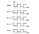
- FIG. 3 is a timing chart for explaining the switching of the MOSFET 20.
- the high level voltage is indicated by “H” and the low level voltage is indicated by “L”.
- the transition of the voltage of the control signal and the transition of the states of the second switch 26, the third switch 40, the first switch 22 and the MOSFET 20 are shown. Time is shown on the horizontal axis for these transitions.
- the microcomputer 30 When the voltage of the control signal exceeds zero V, the current flows from the microcomputer 30 in the order of the second switch resistors 28 and 27, and returns to the microcomputer 30.
- the microcomputer 30 switches the voltage of the control signal from the high level voltage to the low level voltage.
- the voltage of the control signal is a low level voltage, the current flowing through the second switch resistor is small enough or zero A. Therefore, in the second switch 26, the base voltage based on the potential of the emitter is sufficiently low or is zero V, which is less than the first voltage threshold value. Therefore, the second switch 26 is off.
- the third switch 40 When the second switch 26 is off, no current flows through the third switch resistors 41 and 42. Therefore, in the third switch 40, the base voltage based on the potential of the emitter is zero V, which is equal to or higher than the third voltage threshold value. Therefore, the third switch 40 is off.
- the switching circuit 25 switches the first switch 22 off when the second switch 26 is switched off.
- the gate voltage based on the potential of the ground conductor 16 is the power supply voltage.
- a current related to noise flows through the second conductor 15, or when the contact resistance of the second conductor 15 increases in the ground conductor 16, one end of the second conductor 15 based on the potential of the ground conductor 16, that is, the MOSFET 20
- the voltage of the source fluctuates.
- the power supply voltage is sufficiently larger than the maximum value of the source voltage of the MOSFET 20 with respect to the potential of the ground conductor 16. The difference between this maximum value and the power supply voltage is greater than or equal to the gate threshold. Therefore, when the first switch 22 is off, in the MOSFET 20, the gate voltage with respect to the source potential is equal to or higher than the gate threshold, and the MOSFET 20 is on.
- the MOSFET 20 When the MOSFET 20 is on, the current flows from the positive electrode of the DC power supply 10 in this order to the load 13, the MOSFET 20, the second conductor 15, and the ground conductor 16 and returns to the negative electrode of the DC power supply 10. As a result, electric power is supplied to the load 13 and the load 13 operates. At this time, a current is input to the drain of the MOSFET 20 and a current is output from the source of the MOSFET 20.
- the current path of the current flowing in this order from the positive electrode of the DC power supply 10 to the load 13, the MOSFET 20, the second conductor 15, and the ground conductor 16 is the current path of the current flowing through the load 13.
- the MOSFET 20 is arranged on the downstream side of the load 13 in this current path.
- the microcomputer 30 switches the voltage of the control signal from the low level voltage to the high level voltage.
- the voltage of the control signal is a high level voltage
- the current flowing in the order of the second switch resistors 28 and 27 is sufficiently large. Therefore, when the voltage of the control signal is a high level voltage, in the second switch 26, the base voltage based on the potential of the emitter is equal to or higher than the second voltage threshold value, and the second switch 26 is on.
- the second switch 26 When the second switch 26 is on, the current flows from the positive electrode of the DC power supply 10 in the order of the third switch resistors 41 and 42, the second switch 26, the first conductor 14 and the ground conductor 16, and the negative electrode of the DC power supply 10. Return to. As a result, a voltage drop occurs in the third switch resistor 41, and in the third switch 40, the base voltage based on the potential of the emitter is less than the third voltage threshold value. As a result, when the second switch 26 is on, the third switch 40 is on.
- the collector, emitter and base each function as an input end, an output end and a control end.
- the third switch 40 When the third switch 40 is on, the current flows from the positive electrode of the DC power supply 10 in the order of the third switch 40, the first switch resistors 24 and 23, the second conductor 15 and the ground conductor 16, and the negative electrode of the DC power supply 10. Return to. As a result, a voltage drop occurs in the first switch resistor 23, and in the first switch 22, the base voltage based on the potential of the emitter is equal to or higher than the first voltage threshold. As a result, when the third switch 40 is on, the first switch 22 is on. The switching circuit 25 switches the first switch 22 on when the second switch 26 is switched on.
- the power supply voltage is sufficiently larger than the maximum value of the voltage of the source of the MOSFET 20 based on the potential of the ground conductor 16, that is, the emitter of the first switch 22. Therefore, the current flowing through the first switch resistor 23 is large, and the width of the voltage drop in the first switch resistor 23 is equal to or larger than the first voltage threshold value. Therefore, when the third switch 40 is on, the first switch 22 is surely switched on.
- the emitter, collector and base each function as an input end, an output end and a control end.
- the gate voltage with respect to the source potential is zero V, which is less than the gate threshold. Therefore, when the first switch 22 is on, the MOSFET 20 is off.
- the MOSFET 20 when the voltage of the control signal is a low level voltage, that is, when the microcomputer 30 outputs the low level voltage to the gate of the second switch 26, the MOSFET 20 is on.
- the voltage of the control signal is a high level voltage, that is, when the microcomputer 30 outputs the high level voltage to the gate of the second switch 26, the MOSFET 20 is off.
- the current flows from the positive electrode of the DC power supply 10 in the order of the circuit resistance 21, the first switch 22, the second conductor 15, and the ground conductor 16 and returns to the negative electrode of the DC power supply 10.
- a current is input to the collector of the first switch 22, and a current is output from the emitter of the first switch 22.
- the collector, emitter and base each function as an input end, an output end and a control end.
- the emitter of the second switch 26 When the first conductor 14 is disconnected, or when the connection between the drive device 11 and the ground conductor 16 via the first conductor 14 is disconnected, the emitter of the second switch 26 is opened. In this case, since no current flows through the second switch resistor 27, the base voltage of the second switch 26 with reference to the potential of the emitter is zero V, which is less than the second voltage threshold. At this time, the second switch 26 is off. As described above, when the second switch 26 is off, the third switch 40 and the first switch 22 are off and the MOSFET 20 is on. Therefore, when the emitter of the second switch 26 is opened, the MOSFET 20 is kept on.
- the high-level voltage and the low-level voltage output by the microcomputer 30 to the second switch 26 are voltages based on the potential of the emitter of the second switch 26.
- the second switch 26 is switched on or off according to the voltage of the base based on the potential of the emitter. Therefore, even when the reference potentials of the high level voltage and the low level voltage, that is, the voltage of the emitter of the second switch 26 with reference to the potential of the ground conductor 16 fluctuates, the second switch 26 is turned on without error. Or switch off.
- the power supply voltage of the DC power supply 10 is sufficiently higher than the maximum value of the voltage at one end of the first conductor 14 based on the potential of the ground conductor 16. Therefore, when the second switch 26 is on, a sufficiently large current flows through the third switch resistor 41, and in the third switch 40, the base voltage based on the potential of the emitter is less than the third voltage threshold value. .. As a result, when the second switch 26 is switched on, the third switch 40 is switched on regardless of the voltage at one end of the first conductor 14 with reference to the potential of the ground conductor 16. As described above, when the third switch 40 is switched on, the first switch 22 is switched on and the MOSFET 20 is switched off.
- the second switch 26 When the second switch 26 is switched off, the current flow is stopped through the third switch resistor 41 regardless of the voltage at one end of the first conductor 14 with respect to the potential of the ground conductor 16, and the second switch 26 is turned off.
- the 3 switch 40 is switched off.
- the third switch 40 when the third switch 40 is switched off, the first switch 22 is switched off and the MOSFET 20 is switched on.
- the switching of the MOSFET 20 is also performed without an error.
- the reference potential of the voltage of the control signal that is, the voltage at one end of the first conductor 14 with reference to the potential of the ground conductor 16 fluctuates, the MOSFET 20 is switched on or off without error.
- the MOSFET 20 may be a switch that is switched on by increasing the voltage at the control end with reference to the potential at the output end at which the current is output. Therefore, instead of the MOSFET 20, an N-channel type FET, an IGBT (Insulated Gate Bipolar Transistor), an NPN-type bipolar transistor, or the like different from the MOSFET may be used.
- an N-channel type FET an IGBT (Insulated Gate Bipolar Transistor), an NPN-type bipolar transistor, or the like different from the MOSFET may be used.
- the number of switches used to control the power supply of the load 13 is one.
- the number of switches used to control the power supply of the load 13 is not limited to 1, and may be 2 or more.
- the second embodiment will be described as different from the first embodiment. Other configurations except the configuration described later are common to the first embodiment. Therefore, the same reference reference numerals as those in the first embodiment are assigned to the components common to the first embodiment, and the description thereof will be omitted.
- FIG. 4 is a block diagram showing a main configuration of the drive device 11 according to the second embodiment.
- the drive device 11 drives the motor M as the load 13.
- the power supply system 1 in the second embodiment does not have to have the electric device 12 as in the first embodiment.
- the drive device 11 includes a first upstream switch 50u, a first downstream switch 50d, a second upstream switch 51u, and a second downstream switch 51d.
- a first current path and a second current path are provided as current paths of the current flowing from the positive electrode of the DC power supply 10 via the motor M.
- the first upstream switch 50u and the first downstream switch 50d are arranged on the upstream side and the downstream side of the motor M, respectively.
- the second upstream switch 51u and the second downstream switch 51d are arranged on the upstream side and the downstream side of the motor M, respectively.
- the direction of the current flowing through the motor M when the current is flowing through the first current path is the first direction, and is downward in FIG.
- the direction of the current flowing through the motor M when the current is flowing through the second current path is the second direction, which is upward in FIG.
- the first direction is different from the second direction.
- the drive device 11 switches the first upstream switch 50u and the first downstream switch 50d on while the second upstream switch 51u and the second downstream switch 51d are off.
- a current in the first direction flows through the motor M, and the motor M rotates in the positive direction.
- Motor M has a columnar rotor.
- the rotation of the motor M means the rotation around the axis of the rotor.
- the positive direction is, for example, a clockwise direction.
- the drive device 11 switches the second upstream switch 51u and the second downstream switch 51d on while the first upstream switch 50u and the first downstream switch 50d are off.
- a current in the second direction flows through the motor M, and the motor M rotates in the opposite direction.
- the forward direction is clockwise, the reverse direction is counterclockwise.
- the motor M is used, for example, to open and close the windows of the vehicle. When the motor M rotates in the forward direction, for example, the window of the vehicle is opened. When the motor M rotates in the opposite direction, for example, the window of the vehicle is closed.
- the drive device 11 switches off the first upstream switch 50u and the second upstream switch 51u. As a result, the power supply from the DC power supply 10 to the motor M is stopped, and the motor M stops operating.
- the drive device 11 includes a regulator 29, a microcomputer 30, and a first upstream drive circuit in addition to the first upstream switch 50u, the first downstream switch 50d, the second upstream switch 51u, and the second downstream switch 51d. It has 52u, a first downstream drive circuit 52d, a second upstream drive circuit 53u, a second downstream drive circuit 53d, and switch resistors 54 and 55.
- the first upstream switch 50u, the first downstream switch 50d, the second upstream switch 51u, and the second downstream switch 51d are N-channel MOSFETs, respectively.
- the DC power supply 10, the regulator 29, the microcomputer 30, the first conductor 14, and the ground conductor 16 are connected in the same manner as in the first embodiment.
- a plurality of electric devices 12 are connected to one end of the first conducting wire 14.
- the drain of the first upstream switch 50u is connected to the positive electrode of the DC power supply 10.
- the source of the first upstream switch 50u is connected to one end of the motor M.
- the other end of the motor M is connected to the drain of the first downstream switch 50d.
- the source of the first downstream switch 50d is connected to the ground conductor 16 via the second conductor 15.
- a switch resistor 54 is connected between the gate and the source of the first downstream switch 50d.
- the drain of the second upstream switch 51u is connected to the positive electrode of the DC power supply 10.
- the source of the second upstream switch 51u is connected to the connection node between the first downstream switch 50d and the motor M.
- the connection node between the first upstream switch 50u and the motor M is connected to the drain of the second downstream switch 51d.
- the source of the second downstream switch 51d is connected to the ground conductor 16 via the second conductor 15.
- a switch resistor 55 is connected between the gate and the source of the second downstream switch 51d.
- the gates of the first upstream switch 50u, the first downstream switch 50d, the second upstream switch 51u, and the second downstream switch 51d are the first upstream drive circuit 52u, the first downstream drive circuit 52d, the second upstream drive circuit 53u, and the second upstream drive circuit 53u. 2 It is connected to the downstream drive circuit 53d.
- the first upstream drive circuit 52u is connected to the microcomputer 30.
- the connection node between the first upstream drive circuit 52u and the microcomputer 30 is connected to the second downstream drive circuit 53d.
- the second upstream drive circuit 53u is connected to the microcomputer 30.
- the connection node between the second upstream drive circuit 53u and the microcomputer 30 is connected to the first downstream drive circuit 52d.
- the microcomputer 30 is further directly connected to each of the first downstream drive circuit 52d and the second downstream drive circuit 53d.
- the first downstream drive circuit 52d and the second downstream drive circuit 53d are each connected to a connection node between the microcomputer 30 and the first conductor 14.
- the first downstream drive circuit 52d is further connected to the source of the first downstream switch 50d.
- the second downstream drive circuit 53d is further connected to the source of the second downstream switch 51d.
- Each of the first downstream drive circuit 52d and the second downstream drive circuit 53d is connected to the positive electrode of the DC power supply 10. In order to prevent the drawings from becoming complicated, the description of these connecting lines is omitted in FIG.
- the resistance between the drain and the source when the gate voltage based on the source potential is less than the switch threshold.
- the value is large enough.
- the first upstream switch 50u, the first downstream switch 50d, the second upstream switch 51u, and the second downstream switch 51d are each off, and no current flows through the drain and the source.
- the switch threshold is a positive constant value and is preset.
- the switch thresholds of the first upstream switch 50u, the first downstream switch 50d, the second upstream switch 51u, and the second downstream switch 51d may be the same as or different from the other switch thresholds. May be good.
- the microcomputer 30 outputs a right-side control signal to the first upstream drive circuit 52u and the second downstream drive circuit 53d.
- the microcomputer 30 outputs the left side control signal to the second upstream drive circuit 53u and the first downstream drive circuit 52d.
- the right side control signal and the left side control signal are composed of a high level voltage and a low level voltage, respectively.
- the microcomputer 30 switches the voltage of the right side control signal and the voltage of the left side control signal to a high level voltage or a low level voltage, respectively.
- Each of the first upstream drive circuit 52u and the second downstream drive circuit 53d is switched on or off according to the voltage of the right control signal.
- Each of the second upstream drive circuit 53u and the first downstream drive circuit 52d is switched on or off according to the voltage of the left side control signal.
- FIG. 5 is a timing chart for explaining the operation of the drive device 11. Also in FIG. 5, the high level voltage is indicated by “H” and the low level voltage is indicated by “L”. The transition of the right side control signal and the left side control signal, and the transition of the states of the first upstream switch 50u, the first downstream switch 50d, the second upstream switch 51u, and the second downstream switch 51d are shown. Time is shown on the horizontal axis for these transitions.
- the first state is a state in which the voltages of the right side control signal and the left side control signal are high level voltage and low level voltage, respectively.
- the second state is a state in which the voltages of the right side control signal and the left side control signal are the low level voltage and the high level voltage, respectively.
- the third state is a state in which the voltage of the right side control signal and the left side control signal is a low level voltage.
- the first upstream drive circuit 52u raises the gate voltage of the first upstream switch 50u with reference to the potential of the ground conductor 16.
- the first upstream switch 50u the voltage of the gate based on the potential of the source becomes equal to or higher than the switch threshold value, and the first upstream switch 50u is switched on.
- the second downstream drive circuit 53d reduces the gate voltage relative to the source potential to zero V in the second downstream switch 51d.
- the second downstream switch 51d the voltage of the gate based on the potential of the source becomes less than the switch threshold value, and the second downstream switch 51d is switched off. Therefore, when the voltage of the right side control signal is a high level voltage, the first upstream switch 50u and the second downstream switch 51d are on and off, respectively.
- the second upstream drive circuit 53u lowers the gate voltage of the second upstream switch 51u with reference to the potential of the ground conductor 16.
- the first downstream drive circuit 52d raises the gate voltage relative to the source potential at the first downstream switch 50d.
- the voltage of the gate based on the potential of the source becomes equal to or higher than the switch threshold value, and the first downstream switch 50d is switched on. Therefore, when the voltage of the left side control signal is a low level voltage, the second upstream switch 51u and the first downstream switch 50d are off and on, respectively.
- the first upstream switch 50u and the first downstream switch 50d are on, and the second upstream switch 51u and the second downstream switch are on. 51d is off.
- the current flows from the positive electrode of the DC power supply 10 in the order of the first upstream switch 50u, the motor M, the first downstream switch 50d, the second conductor 15, and the ground conductor 16 and returns to the negative electrode of the DC power supply 10.
- the current in the first direction flows through the motor M, and the motor M rotates in the positive direction.
- the first upstream drive circuit 52u lowers the gate voltage of the first upstream switch 50u with reference to the potential of the ground conductor 16.
- the first upstream switch 50u the voltage of the gate based on the potential of the source becomes less than the switch threshold value, and the first upstream switch 50u is switched off.
- the second downstream drive circuit 53d raises the gate voltage relative to the source potential at the second downstream switch 51d.
- the second downstream switch 51d the voltage of the gate based on the potential of the source becomes equal to or higher than the switch threshold value, and the second downstream switch 51d is switched on. Therefore, when the voltage of the right side control signal is a low level voltage, the first upstream switch 50u and the second downstream switch 51d are off and on, respectively.
- the second upstream drive circuit 53u raises the gate voltage of the second upstream switch 51u with reference to the potential of the ground conductor 16.
- the first downstream drive circuit 52d reduces the gate voltage relative to the source potential to zero V in the first downstream switch 50d.
- the voltage of the gate based on the potential of the source becomes less than the switch threshold value, and the first downstream switch 50d is switched off. Therefore, when the voltage of the left side control signal is a high level voltage, the second upstream switch 51u and the first downstream switch 50d are on and off, respectively.
- the first upstream switch 50u and the first downstream switch 50d are off, and the second upstream switch 51u and the second downstream switch are off. 51d is on.
- the current flows from the positive electrode of the DC power supply 10 in the order of the second upstream switch 51u, the motor M, the second downstream switch 51d, the second conductor 15, and the ground conductor 16 and returns to the negative electrode of the DC power supply 10.
- the current in the second direction flows through the motor M, and the motor M rotates in the opposite direction.
- the first upstream switch 50u and the second upstream switch 51u are off, and the first downstream switch 50d and the second downstream switch 51d are on. .. Since the first upstream switch 50u and the second upstream switch 51u are off, power is not supplied to the motor M, and the motor M stops operating.
- Motor M has an inductor (not shown). While power is being supplied to the motor M, the current flows through the inductor and energy is stored in the inductor. When the first downstream switch 50d and the second downstream switch 51d are on, a current flows from one end of the motor M through the first downstream switch 50d and the second downstream switch 51d, and the motor M releases energy. As shown in FIG. 5, when the direction in which the motor M rotates is changed, the operation of the motor M is temporarily stopped, and the motor M is made to release energy.
- FIG. 6 is a circuit diagram of the first downstream drive circuit 52d.
- the first downstream drive circuit 52d includes a circuit resistor 21, a first switch 22, a first switch resistor 23, 24, a switching circuit 25, a second switch 26, a second switch resistor 27, 28, and a circuit switch 60.
- the switching circuit 25 in the second embodiment has a third switch 40 and third switch resistors 41 and 42 as in the first embodiment.
- the circuit resistance 21, the first switch 22, the first switch resistance 23, 24, the switching circuit 25, the second switch 26, the second switch resistance 27, 28, the third switch 40, and the third switch resistance 41, 42 are connected. It is the same as the first form.
- One end of the circuit switch 60 is connected to the positive electrode of the DC power supply 10.
- the other end of the circuit switch 60 is connected to a connection node between the circuit resistor 21 and the collector of the third switch 40.
- the connection node between the circuit resistor 21 and the collector of the first switch 22 is connected to the gate of the first downstream switch 50d.
- the emitter of the first switch 22 is connected to the source of the first downstream switch 50d.
- the base of the second switch 26 is connected to the microcomputer 30 via the second switch resistor 28, and the emitter of the second switch 26 is connected to one end of the first conductor 14. ..
- the circuit resistor 21 is connected between the positive electrode of the DC power supply 10 and the gate of the first downstream switch 50d.
- the first switch 22 is connected between the gate and the source of the first downstream switch 50d.
- the microcomputer 30 switches the circuit switch 60 on or off.
- the microcomputer 30 outputs the left side control signal to the base of the second switch 26.
- the high level voltage and the low level voltage of the left side control signal are voltages with reference to the emitter of the second switch 26. Therefore, when the circuit switch 60 is on, the second switch 26, the third switch 40, and the first switch 22 are switched on or off according to the voltage of the left side control signal.
- the second switch 26, the third switch 40, and the first switch 22 are off as in the first embodiment.
- the current flows from the positive electrode of the DC power supply 10 in the order of the circuit resistance 21, the switch resistance 54, the second conductor 15, and the ground conductor 16 and returns to the negative electrode of the DC power supply 10.
- a voltage drop occurs at the switch resistor 54.
- the first downstream switch 50d the voltage of the gate based on the potential of the source is equal to or higher than the switch threshold value, and the first downstream switch 50d is on.
- the power supply voltage is sufficiently larger than the maximum value of the source voltage of the first downstream switch 50d based on the potential of the ground conductor 16. Therefore, the width of the voltage drop that occurs in the switch resistor 54 is equal to or larger than the switch threshold value. Therefore, when the first switch 22 is off, the first downstream switch 50d is surely switched on.
- the second switch 26, the third switch 40, and the first switch 22 are on as in the first embodiment.
- the gate voltage relative to the source potential is zero V, which is less than the switch threshold.
- the first downstream switch 50d is off.
- the power supply voltage is sufficiently larger than the maximum value of the voltage of the emitter of the first switch 22 with respect to the potential of the ground conductor 16 as in the first embodiment. Therefore, when the second switch 26 is on, the width of the voltage drop that occurs in the first switch resistor 23 is equal to or larger than the first current threshold value. Therefore, when the third switch 40 is on, the first switch 22 is surely switched on.
- the circuit switch 60 when the circuit switch 60 is on, as shown in FIG. 5, when the voltage of the left side control signal is the low level voltage, the first downstream switch 50d is on. In a similar case, when the voltage of the left side control signal is a high level voltage, the first downstream switch 50d is off.
- the microcomputer 30 can switch the second upstream switch 51u and the first downstream switch 50d off.
- the second downstream drive circuit 53d is configured in the same manner as the first downstream drive circuit 52d.
- the connection of the second downstream drive circuit 53d can be described by replacing the first downstream switch 50d with the second downstream switch 51d.
- the operation of the second downstream drive circuit 53d is the same as the operation of the first downstream drive circuit 52d.
- the second downstream drive is performed by replacing the left side control signal, the first downstream switch 50d, and the switch resistance 54 with the right side control signal, the second downstream switch 51d, and the switch resistance 55, respectively.
- the operation of the circuit 53d can be described.
- the voltage of the right side control signal is a voltage based on the potential of the emitter of the second switch 26 included in the second downstream drive circuit 53d.
- the second downstream switch 51d is on when the voltage of the right side control signal is a low level voltage. In the same case, when the voltage of the right side control signal is a high level voltage, the second downstream switch 51d is off.
- the microcomputer 30 turns off the first upstream switch 50u and the second downstream switch 51d. It can be switched.
- the microcomputer 30 switches the voltage of the right side control signal and the left side control signal to a low level voltage, and switches off the circuit switch 60 of the first downstream drive circuit 52d and the second downstream drive circuit 53d. As a result, it is possible to realize a state in which the first upstream switch 50u, the first downstream switch 50d, the second upstream switch 51u, and the second downstream switch 51d are off.
- the drive device 11 according to the second embodiment similarly exhibits the effect of the drive device 11 according to the first embodiment. Therefore, when the circuit switch 60 is on, when the reference potential of the voltage of each of the right side control signal and the left side control signal, that is, the voltage at one end of the first conductor 14 with reference to the potential of the ground conductor 16 fluctuates. Even if there is, the first downstream switch 50d and the second downstream switch 51d are switched on or off without error. When the circuit switch 60 is off, the first downstream switch 50d and the second downstream switch 51d are off regardless of the voltage at one end of the first conductor 14 with respect to the potential of the ground conductor 16.
- each of the first upstream switch 50u and the second upstream switch 51u may function as a switch, and thus is not limited to the N-channel type MOSFET, and is an N-channel type FET and a P-channel type different from the MOSFET. FET, IGBT, bipolar transistor, relay contact, etc. may be used.
- Each of the first downstream switch 50d and the second downstream switch 51d may be a switch that is switched on by increasing the voltage at the control end with reference to the potential at the output end from which the current is output.
- each of the first downstream switch 50d and the second downstream switch 51d is not limited to the N-channel type MOSFET, and may be an N-channel type FET, an IGBT, an NPN type bipolar transistor, or the like different from the MOSFET. ..
- the load driven by the drive device 11 is not limited to the motor M, and may be any electric device that switches the direction in which the DC voltage is applied.
- a resistor may be connected between the gate and the source of the MOSFET 20.
- a current flows from the positive electrode of the DC power supply 10 in the order of the circuit resistor 21, the resistor, and the ground conductor 16, and returns to the negative electrode of the DC power supply 10. Since a voltage drop occurs in the resistor, in the MOSFET 20, the gate voltage relative to the source potential is greater than or equal to the gate threshold, and the MOSFET 20 is on.
- the first switch 22 and the second switch 26 may be switches that are switched on by increasing the voltage at the control end with reference to the potential at the output end from which the current is output. .. Therefore, each of the first switch 22 and the second switch 26 is not limited to the NPN type bipolar transistor, and may be an N channel type FET, an IGBT, or the like.
- the third switch 40 may be a switch that is switched on by lowering the voltage at the control end with reference to the potential at the output end from which the current is output. Therefore, the third switch 40 is not limited to the PNP type bipolar transistor, and may be, for example, a P channel type FET.
- the number of electric devices 12 included in the power supply system 1 in the first and second embodiments is not limited to two or more, and may be one.
Landscapes
- Engineering & Computer Science (AREA)
- Power Engineering (AREA)
- Electronic Switches (AREA)
- Direct Current Feeding And Distribution (AREA)
Priority Applications (3)
| Application Number | Priority Date | Filing Date | Title |
|---|---|---|---|
| CN202080083012.9A CN114762253B (zh) | 2019-12-19 | 2020-12-02 | 驱动装置 |
| US17/757,556 US11881850B2 (en) | 2019-12-19 | 2020-12-02 | Driving apparatus |
| DE112020006206.6T DE112020006206T5 (de) | 2019-12-19 | 2020-12-02 | Ansteuervorrichtung |
Applications Claiming Priority (2)
| Application Number | Priority Date | Filing Date | Title |
|---|---|---|---|
| JP2019-229585 | 2019-12-19 | ||
| JP2019229585A JP7310591B2 (ja) | 2019-12-19 | 2019-12-19 | 駆動装置 |
Publications (1)
| Publication Number | Publication Date |
|---|---|
| WO2021124893A1 true WO2021124893A1 (ja) | 2021-06-24 |
Family
ID=76431739
Family Applications (1)
| Application Number | Title | Priority Date | Filing Date |
|---|---|---|---|
| PCT/JP2020/044839 Ceased WO2021124893A1 (ja) | 2019-12-19 | 2020-12-02 | 駆動装置 |
Country Status (5)
| Country | Link |
|---|---|
| US (1) | US11881850B2 (https=) |
| JP (1) | JP7310591B2 (https=) |
| CN (1) | CN114762253B (https=) |
| DE (1) | DE112020006206T5 (https=) |
| WO (1) | WO2021124893A1 (https=) |
Families Citing this family (1)
| Publication number | Priority date | Publication date | Assignee | Title |
|---|---|---|---|---|
| KR20180101595A (ko) | 2016-02-01 | 2018-09-12 | 프리벤치오 인코포레이티드 | 심혈관 질환 및 사건을 위한 진단학적 및 예후적 방법 |
Citations (6)
| Publication number | Priority date | Publication date | Assignee | Title |
|---|---|---|---|---|
| JPH07240676A (ja) * | 1994-03-01 | 1995-09-12 | Toyota Motor Corp | 駆動回路 |
| JPH1022803A (ja) * | 1996-07-03 | 1998-01-23 | Denso Corp | nチャネルMOSFETの駆動回路及び電流方向切換回路 |
| US20070252637A1 (en) * | 2006-04-28 | 2007-11-01 | Innolux Display Corp. | Power switching circuit and liquid crystal display using same |
| JP2012129978A (ja) * | 2010-11-22 | 2012-07-05 | Denso Corp | 負荷駆動装置 |
| JP2017073657A (ja) * | 2015-10-07 | 2017-04-13 | ローム株式会社 | 誤出力防止回路 |
| JP2017212522A (ja) * | 2016-05-24 | 2017-11-30 | ルネサスエレクトロニクス株式会社 | 半導体装置 |
Family Cites Families (11)
| Publication number | Priority date | Publication date | Assignee | Title |
|---|---|---|---|---|
| JPS5927329A (ja) * | 1982-08-05 | 1984-02-13 | Nec Corp | 電源確定信号発生回路 |
| JPS63311818A (ja) * | 1987-06-12 | 1988-12-20 | Matsushita Electric Ind Co Ltd | Ttl回路 |
| JPH01194606A (ja) * | 1988-01-29 | 1989-08-04 | Hitachi Ltd | Mosfetのドライブ回路 |
| JPH0697375A (ja) * | 1992-09-17 | 1994-04-08 | Toshiba Corp | 電力用半導体装置 |
| JP3678208B2 (ja) * | 2002-04-19 | 2005-08-03 | 株式会社デンソー | 負荷駆動用半導体装置 |
| JP2005168234A (ja) * | 2003-12-04 | 2005-06-23 | Toyota Industries Corp | 駆動回路 |
| JP5618181B2 (ja) | 2010-03-31 | 2014-11-05 | スズキ株式会社 | リレー駆動回路 |
| JP5459168B2 (ja) * | 2010-09-29 | 2014-04-02 | ブラザー工業株式会社 | 出力回路及び出力装置 |
| US8766671B2 (en) | 2010-11-22 | 2014-07-01 | Denso Corporation | Load driving apparatus |
| JP6724539B2 (ja) * | 2016-05-16 | 2020-07-15 | 住友電装株式会社 | 負荷駆動装置 |
| JP2018085567A (ja) * | 2016-11-21 | 2018-05-31 | 株式会社オートネットワーク技術研究所 | スイッチ回路及び電源装置 |
-
2019
- 2019-12-19 JP JP2019229585A patent/JP7310591B2/ja active Active
-
2020
- 2020-12-02 DE DE112020006206.6T patent/DE112020006206T5/de active Pending
- 2020-12-02 WO PCT/JP2020/044839 patent/WO2021124893A1/ja not_active Ceased
- 2020-12-02 CN CN202080083012.9A patent/CN114762253B/zh active Active
- 2020-12-02 US US17/757,556 patent/US11881850B2/en active Active
Patent Citations (6)
| Publication number | Priority date | Publication date | Assignee | Title |
|---|---|---|---|---|
| JPH07240676A (ja) * | 1994-03-01 | 1995-09-12 | Toyota Motor Corp | 駆動回路 |
| JPH1022803A (ja) * | 1996-07-03 | 1998-01-23 | Denso Corp | nチャネルMOSFETの駆動回路及び電流方向切換回路 |
| US20070252637A1 (en) * | 2006-04-28 | 2007-11-01 | Innolux Display Corp. | Power switching circuit and liquid crystal display using same |
| JP2012129978A (ja) * | 2010-11-22 | 2012-07-05 | Denso Corp | 負荷駆動装置 |
| JP2017073657A (ja) * | 2015-10-07 | 2017-04-13 | ローム株式会社 | 誤出力防止回路 |
| JP2017212522A (ja) * | 2016-05-24 | 2017-11-30 | ルネサスエレクトロニクス株式会社 | 半導体装置 |
Also Published As
| Publication number | Publication date |
|---|---|
| JP7310591B2 (ja) | 2023-07-19 |
| JP2021097387A (ja) | 2021-06-24 |
| CN114762253B (zh) | 2025-11-21 |
| US11881850B2 (en) | 2024-01-23 |
| CN114762253A (zh) | 2022-07-15 |
| DE112020006206T5 (de) | 2022-10-13 |
| US20230014972A1 (en) | 2023-01-19 |
Similar Documents
| Publication | Publication Date | Title |
|---|---|---|
| CN108781078B (zh) | 供电控制装置 | |
| CN114448079B (zh) | 电源切换控制系统 | |
| JP4018077B2 (ja) | 電力用スイッチのためのバッテリ逆接続の保護回路 | |
| JP2020014356A (ja) | 半導体装置および電子制御装置 | |
| CN102457164A (zh) | 高压输出驱动器 | |
| CN107086864B (zh) | 驱动器电路、对应的装置和方法 | |
| JP7795325B2 (ja) | ゲート制御回路、半導体装置、電子機器、車両 | |
| JP2006086507A (ja) | 半導体装置 | |
| JP3642113B2 (ja) | nチャネルMOSFETの駆動回路及び電流方向切換回路 | |
| WO2021124893A1 (ja) | 駆動装置 | |
| CN111418148A (zh) | 多相电动机的控制电路 | |
| JP6996446B2 (ja) | 回路装置 | |
| WO2020217780A1 (ja) | 負荷駆動装置 | |
| CN115210984B (zh) | 供电控制装置 | |
| JP2011199401A (ja) | 電源供給装置 | |
| JP4228960B2 (ja) | 負荷駆動装置及び負荷駆動装置の高電圧印加試験方法 | |
| US20250015797A1 (en) | Control device | |
| JP7512904B2 (ja) | スイッチ装置 | |
| JP7349069B2 (ja) | 駆動装置 | |
| JP2016220413A (ja) | アクチュエータ駆動回路 | |
| WO2022244319A1 (ja) | ゲート駆動装置 | |
| WO2021131698A1 (ja) | 給電制御装置 | |
| EP2066016A1 (en) | Static switch for motors of climate control units and climate control unit comprising the switch | |
| JP2009012714A (ja) | モータ制御装置 |
Legal Events
| Date | Code | Title | Description |
|---|---|---|---|
| 121 | Ep: the epo has been informed by wipo that ep was designated in this application |
Ref document number: 20902679 Country of ref document: EP Kind code of ref document: A1 |
|
| 122 | Ep: pct application non-entry in european phase |
Ref document number: 20902679 Country of ref document: EP Kind code of ref document: A1 |