WO2021111604A1 - 半導体装置 - Google Patents
半導体装置 Download PDFInfo
- Publication number
- WO2021111604A1 WO2021111604A1 PCT/JP2019/047688 JP2019047688W WO2021111604A1 WO 2021111604 A1 WO2021111604 A1 WO 2021111604A1 JP 2019047688 W JP2019047688 W JP 2019047688W WO 2021111604 A1 WO2021111604 A1 WO 2021111604A1
- Authority
- WO
- WIPO (PCT)
- Prior art keywords
- power supply
- supply line
- wiring
- power
- semiconductor device
- Prior art date
- Legal status (The legal status is an assumption and is not a legal conclusion. Google has not performed a legal analysis and makes no representation as to the accuracy of the status listed.)
- Ceased
Links
Images


Classifications
-
- H—ELECTRICITY
- H10—SEMICONDUCTOR DEVICES; ELECTRIC SOLID-STATE DEVICES NOT OTHERWISE PROVIDED FOR
- H10D—INORGANIC ELECTRIC SEMICONDUCTOR DEVICES
- H10D89/00—Aspects of integrated devices not covered by groups H10D84/00 - H10D88/00
- H10D89/10—Integrated device layouts
-
- H—ELECTRICITY
- H10—SEMICONDUCTOR DEVICES; ELECTRIC SOLID-STATE DEVICES NOT OTHERWISE PROVIDED FOR
- H10D—INORGANIC ELECTRIC SEMICONDUCTOR DEVICES
- H10D84/00—Integrated devices formed in or on semiconductor substrates that comprise only semiconducting layers, e.g. on Si wafers or on GaAs-on-Si wafers
- H10D84/90—Masterslice integrated circuits
- H10D84/903—Masterslice integrated circuits comprising field effect technology
- H10D84/907—CMOS gate arrays
-
- H—ELECTRICITY
- H01—ELECTRIC ELEMENTS
- H01L—SEMICONDUCTOR DEVICES NOT COVERED BY CLASS H10
- H01L23/00—Details of semiconductor or other solid state devices
- H01L23/52—Arrangements for conducting electric current within the device in operation from one component to another, i.e. interconnections, e.g. wires, lead frames
- H01L23/522—Arrangements for conducting electric current within the device in operation from one component to another, i.e. interconnections, e.g. wires, lead frames including external interconnections consisting of a multilayer structure of conductive and insulating layers inseparably formed on the semiconductor body
- H01L23/528—Layout of the interconnection structure
- H01L23/5286—Arrangements of power or ground buses
-
- H—ELECTRICITY
- H01—ELECTRIC ELEMENTS
- H01L—SEMICONDUCTOR DEVICES NOT COVERED BY CLASS H10
- H01L23/00—Details of semiconductor or other solid state devices
- H01L23/52—Arrangements for conducting electric current within the device in operation from one component to another, i.e. interconnections, e.g. wires, lead frames
- H01L23/535—Arrangements for conducting electric current within the device in operation from one component to another, i.e. interconnections, e.g. wires, lead frames including internal interconnections, e.g. cross-under constructions
-
- H—ELECTRICITY
- H01—ELECTRIC ELEMENTS
- H01L—SEMICONDUCTOR DEVICES NOT COVERED BY CLASS H10
- H01L23/00—Details of semiconductor or other solid state devices
- H01L23/48—Arrangements for conducting electric current to or from the solid state body in operation, e.g. leads, terminal arrangements ; Selection of materials therefor
- H01L23/481—Internal lead connections, e.g. via connections, feedthrough structures
-
- H—ELECTRICITY
- H10—SEMICONDUCTOR DEVICES; ELECTRIC SOLID-STATE DEVICES NOT OTHERWISE PROVIDED FOR
- H10D—INORGANIC ELECTRIC SEMICONDUCTOR DEVICES
- H10D84/00—Integrated devices formed in or on semiconductor substrates that comprise only semiconducting layers, e.g. on Si wafers or on GaAs-on-Si wafers
- H10D84/80—Integrated devices formed in or on semiconductor substrates that comprise only semiconducting layers, e.g. on Si wafers or on GaAs-on-Si wafers characterised by the integration of at least one component covered by groups H10D12/00 or H10D30/00, e.g. integration of IGFETs
- H10D84/82—Integrated devices formed in or on semiconductor substrates that comprise only semiconducting layers, e.g. on Si wafers or on GaAs-on-Si wafers characterised by the integration of at least one component covered by groups H10D12/00 or H10D30/00, e.g. integration of IGFETs of only field-effect components
- H10D84/83—Integrated devices formed in or on semiconductor substrates that comprise only semiconducting layers, e.g. on Si wafers or on GaAs-on-Si wafers characterised by the integration of at least one component covered by groups H10D12/00 or H10D30/00, e.g. integration of IGFETs of only field-effect components of only insulated-gate FETs [IGFET]
- H10D84/85—Complementary IGFETs, e.g. CMOS
-
- H—ELECTRICITY
- H10—SEMICONDUCTOR DEVICES; ELECTRIC SOLID-STATE DEVICES NOT OTHERWISE PROVIDED FOR
- H10D—INORGANIC ELECTRIC SEMICONDUCTOR DEVICES
- H10D84/00—Integrated devices formed in or on semiconductor substrates that comprise only semiconducting layers, e.g. on Si wafers or on GaAs-on-Si wafers
- H10D84/90—Masterslice integrated circuits
- H10D84/903—Masterslice integrated circuits comprising field effect technology
- H10D84/907—CMOS gate arrays
- H10D84/968—Macro-architecture
- H10D84/974—Layout specifications, i.e. inner core regions
- H10D84/975—Wiring regions or routing
-
- H—ELECTRICITY
- H10—SEMICONDUCTOR DEVICES; ELECTRIC SOLID-STATE DEVICES NOT OTHERWISE PROVIDED FOR
- H10D—INORGANIC ELECTRIC SEMICONDUCTOR DEVICES
- H10D84/00—Integrated devices formed in or on semiconductor substrates that comprise only semiconducting layers, e.g. on Si wafers or on GaAs-on-Si wafers
- H10D84/90—Masterslice integrated circuits
- H10D84/903—Masterslice integrated circuits comprising field effect technology
- H10D84/907—CMOS gate arrays
- H10D84/968—Macro-architecture
- H10D84/974—Layout specifications, i.e. inner core regions
- H10D84/981—Power supply lines
-
- H—ELECTRICITY
- H10—SEMICONDUCTOR DEVICES; ELECTRIC SOLID-STATE DEVICES NOT OTHERWISE PROVIDED FOR
- H10D—INORGANIC ELECTRIC SEMICONDUCTOR DEVICES
- H10D84/00—Integrated devices formed in or on semiconductor substrates that comprise only semiconducting layers, e.g. on Si wafers or on GaAs-on-Si wafers
- H10D84/90—Masterslice integrated circuits
- H10D84/903—Masterslice integrated circuits comprising field effect technology
- H10D84/907—CMOS gate arrays
- H10D84/992—Noise prevention, e.g. preventing crosstalk
Definitions
- This disclosure relates to semiconductor devices.
- Semiconductor devices include various circuit areas, and there is a standard cell area as an example of the circuit area. Various logic circuits are included in the standard cell area.
- the power supply potential of VDD is supplied to the semiconductor device, the power potential of V VDD is supplied to the logic circuit in the standard cell region, and a switch such as a transistor is connected between the power supply line of VDD and the power supply line of V VDD.
- a switch such as a transistor is connected between the power supply line of VDD and the power supply line of V VDD.
- the switch switches on / off the supply of V VDD power potential to the transistor of the logic circuit.
- the power supply is turned off when it is not necessary to operate the logic circuit, the leakage current generated in the transistors constituting the logic circuit is suppressed, and the power consumption can be reduced.
- a technique has been proposed in which a subordinate semiconductor chip including wiring is attached to the back side of the main semiconductor chip, and a power supply potential is supplied to a transistor of the main semiconductor chip via the wiring of the subordinate semiconductor chip.
- Such a technique is sometimes called BS-PDN (backside-power delivery network).
- An object of the present disclosure is to provide a semiconductor device to which a switch can be appropriately provided.
- the semiconductor device has a first chip having a substrate, a first wiring layer formed on the first surface of the substrate, and the opposite of the first surface of the substrate. It has a second wiring layer formed on a second surface on the side, and the second wiring layer has a first power supply line to which a first power supply potential is supplied and a second power supply.
- the switch and the second switch provided on one of the first power supply line or the third power supply line, and the first chip includes the first power supply line and the first power supply line. It has a first circuit provided between the three power lines.
- the switch can be provided appropriately.
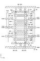
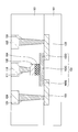
- FIG. 1 is a cross-sectional view showing an outline of a semiconductor device to which the present disclosure is applied.
- FIG. 2 is a diagram showing the layout of the first chip.
- FIG. 3 is a circuit diagram showing a configuration of an example of a circuit included in a semiconductor device.
- FIG. 4 is a circuit diagram showing the configuration of the drive buffer.
- FIG. 5 is a schematic view showing a planar configuration of an example of a drive buffer.
- FIG. 6 is a circuit diagram showing the configuration of the inverter.
- FIG. 7 is a schematic view showing a planar configuration of the inverter.
- FIG. 8 is a schematic view (No. 1) showing a planar configuration of the semiconductor device according to the first embodiment.
- FIG. 9 is a schematic view (No.
- FIG. 10 is a cross-sectional view (No. 1) showing the semiconductor device according to the first embodiment.
- FIG. 11 is a cross-sectional view (No. 2) showing the semiconductor device according to the first embodiment.
- FIG. 12 is a schematic view showing a planar configuration of the semiconductor device according to the first modification of the first embodiment.
- FIG. 13 is a schematic view showing a planar configuration of the semiconductor device according to the second modification of the first embodiment.
- FIG. 14 is a cross-sectional view showing a semiconductor device according to a third modification of the first embodiment.
- FIG. 15 is a circuit diagram showing a configuration of an example of a circuit included in the semiconductor device according to the fourth modification of the first embodiment.
- FIG. 16 is a schematic view (No. 1) showing a planar configuration of the semiconductor device according to the fifth modification of the first embodiment.
- FIG. 17 is a schematic view (No. 2) showing a planar configuration of the semiconductor device according to the fifth modification of the first embodiment.
- FIG. 18 is a schematic view showing a planar configuration of a semiconductor device according to a sixth modification of the first embodiment.
- FIG. 19 is a schematic view (No. 1) showing a planar configuration of the semiconductor device according to the second embodiment.
- FIG. 20 is a schematic view (No. 2) showing a planar configuration of the semiconductor device according to the second embodiment.
- FIG. 21 is a cross-sectional view (No. 1) showing the semiconductor device according to the second embodiment.
- FIG. 22 is a cross-sectional view (No.
- FIG. 23 is a cross-sectional view (No. 1) showing an example of the cross-sectional configuration of the switch transistor.
- FIG. 24 is a cross-sectional view (No. 2) showing an example of the cross-sectional configuration of the switch transistor.
- FIG. 25 is a cross-sectional view (No. 3) showing an example of the cross-sectional configuration of the switch transistor.
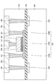
- FIG. 1 is a cross-sectional view showing an outline of a semiconductor device to which the present disclosure is applied.
- the semiconductor device shown in FIG. 1 includes a first chip 10 and a second chip 20.
- the first chip 10 is, for example, a semiconductor chip, and includes a substrate 11 and a first wiring layer 12.
- the substrate 11 is, for example, a silicon substrate, and a semiconductor element such as a transistor is formed on the surface side of the substrate 11.
- the transistor is, for example, a FinFET with fins 13 in the source, drain and channels.
- the first wiring layer 12 is formed on the surface of the substrate 11 and includes the wiring 14 and the insulating layer 15. A part of the wiring 14 is connected to the fin 13. Further, for example, a power supply line 16 connected to the wiring 14 is formed on the front surface side of the substrate 11, and the substrate 11 is provided with a via 17 extending from the power supply line 16 to the back surface of the substrate 11.
- the via 17 is, for example, a through-silicon via (TSV). As shown in FIG. 1, a part of the wiring 14 has a via-like shape and may be connected to the power supply line 16.
- the material of the wiring 14 and the power supply line 16 is, for example, copper, tungsten, cobalt, ruthenium, molybdenum, or the like.
- the second chip 20 is, for example, a semiconductor chip, and is arranged so as to face the back surface of the substrate 11 of the first chip 10.
- the second chip 20 includes, for example, a second wiring layer 22 and a pad 23.
- the second wiring layer 22 includes the wiring 24 and the insulating layer 25.
- the upper surface of the second wiring layer 22 faces, for example, the back surface of the substrate 11 of the first chip 10. That is, the substrate 11 is located between the first wiring layer 12 and the second wiring layer 22.
- the second wiring layer 22 may have a plurality of wirings 24.
- the plurality of wirings 24 may be connected via vias 28 provided in the second wiring layer 22.
- the pad 23 is an external connection terminal connected to, for example, a wiring board or a board.
- a part of the wiring 24 is connected to the via 17.
- the pad 23 is provided on the back surface of the second wiring layer 22, and is connected to the wiring 24 through the via 28.
- the power supply potential is supplied and the signal is transmitted to the second wiring layer 22 via the pad 23.
- the materials of the wiring 24 and the via 28 are, for example, copper, tungsten, cobalt, ruthenium, molybdenum and the like.
- the second chip 20 may have a size similar to that of the first chip 10, or may have a size larger than that of the first chip 10. Further, the pad 23 may be provided on the surface of the second chip 20 on the side facing the first chip 10 and outside the first chip 10 in a plan view.
- the plan view means the plan view of the main surface of the first chip 10.
- the second wiring layer 22 may be provided by forming the wiring 24, the insulating layer 25, and the like on the back surface of the substrate 11.
- the second wiring layer 22 may be formed on the second substrate on which the TSV is formed, or the pad 23 may be provided on the back surface of the second substrate.
- FIG. 1 shows an outline of the semiconductor device, and the details are shown in FIGS. 10, 11, and the like.
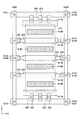
- FIG. 2 is a diagram showing the layout of the first chip 10.
- the first chip 10 includes a first power domain 31A, a second power domain 31B, and an input / output (I / O) cell area 32.
- the I / O cell region 32 is arranged, for example, around the first power domain 31A and the second power domain 31B.
- the number of the first power domain 31A and the number of the second power domain 31B may be 2 or more.
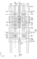
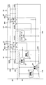
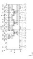
- FIG. 3 is a circuit diagram showing a configuration of an example of a circuit included in a semiconductor device.
- the semiconductor device has a first drive buffer 41, a second drive buffer 42, a third drive buffer 43, and a fourth drive buffer 44 in the first power domain 31A. And have.
- the semiconductor device has a standard cell 56 in the second power domain 31B.
- Semiconductor devices include VDD wiring to which the power potential of VDD is supplied, V VDD wiring to which the power potential of V VDD is supplied, VSS wiring to which the power potential of VSS is supplied, and VVSS wiring to which the power potential of VVSS is supplied. And have.
- the power supply potential of VSS is the ground potential
- the VSS wiring is the ground wiring.
- the power supply potentials of VDD and VSS are supplied to the first to fourth drive buffers 41 to 44 in the first power domain 31A.
- the power potential of V VDD and the power potential of VVSS are supplied to the standard cell 56 in the second power domain 31B.
- the standard cell 56 includes various logic circuits such as a NAND circuit and an inverter.
- the standard cell 56 may include an SRAM (Static Random Access Memory) and a macro.
- the VDD wiring may be connected to the standard cell 56 instead of providing the V VDD wiring, or the VSS wiring may be connected to the standard cell 56 instead of providing the VVSS wiring.
- the standard cell 56 is supplied with the power potential of V VDD and the power potential of VSS, or the power potential of VDD and the power potential of VVSS.
- the semiconductor device includes a first switch transistor 51, a second switch transistor 52, a third switch transistor 53, and a fourth switch transistor 54.
- the first switch transistor 51 is, for example, a P-channel MOS transistor.
- the control signal from the first drive buffer 41 is input to the gate of the first switch transistor 51.
- the source (VDD connection portion) of the first switch transistor 51 is connected to the VDD wiring, and the drain (V VDD connection portion) is connected to the V VDD wiring.
- the second switch transistor 52 is, for example, a P-channel MOS transistor.
- the control signal from the second drive buffer 42 is input to the gate of the second switch transistor 52.
- the second switch transistor 52 is provided on the VDD wiring.
- the first terminal (drain) 521 of the second switch transistor 52 is connected to the source of the first switch transistor 51.
- the first power pad 81 is connected to the source of the first terminal 521 and the first switch transistor 51.
- the power supply potential of VDD is supplied to the first power supply pad 81 from the outside.
- the second power pad 82 is connected to the second terminal (source) 522 of the second switch transistor 52.
- the power supply potential of VDD is supplied to the second power supply pad 82 from the outside.
- the third switch transistor 53 is, for example, an N-channel MOS transistor.
- the control signal from the third drive buffer 43 is input to the gate of the third switch transistor 53.
- the source (VSS connection portion) of the third switch transistor 53 is connected to the VSS wiring, and the drain (VVSS connection portion) is connected to the VVSS wiring.
- the fourth switch transistor 54 is, for example, an N-channel MOS transistor.
- the control signal from the fourth drive buffer 44 is input to the gate of the fourth switch transistor 54.
- the fourth switch transistor 54 is provided on the VSS wiring.
- the first terminal (drain) 541 of the fourth switch transistor 54 is connected to the source of the third switch transistor 53.
- a third power pad 83 is connected to the source of the first terminal 541 and the third switch transistor 53.
- the power supply potential of VSS is supplied to the third power supply pad 83 from the outside.
- the fourth power pad 84 is connected to the second terminal (source) 542 of the fourth switch transistor 54.
- the power potential of VSS is supplied to the fourth power pad 84 from the outside.
- the first to fourth drive buffers 41 to 44 are connected to a control circuit (not shown), and the first to fourth switch transistors 51 to 54 operate in the first to fourth drive buffers 41 to 41. It is controlled by the control circuit via 44.
- the control circuit is provided in the first power domain 31A, and the power supply potential of VDD and the power supply potential of VSS are supplied to the control circuit.
- the control circuit switches the first switch transistor 51 on / off, and controls the continuity between the VDD wiring and the V VDD wiring.
- the control circuit switches the third switch transistor 53 on / off, and controls the continuity between the VSS wiring and the VVSS wiring.
- the control circuit switches the second and fourth switch transistors 52 and 54 on / off, and controls the continuity between the first power domain 31A and the second power domain 31B.
- the second wiring layer 22 has a first sub-wiring layer 201 and a second sub-wiring layer 202.
- the first sub-wiring layer 201 is located closer to the first chip 10 than the second sub-wiring layer 202.
- the first to fourth switch transistors 51 to 54 are provided in the second sub wiring layer 202.
- the first to fourth switch transistors 51 to 54 may be composed of thin film transistors (TFTs) or may be microelectromechanical systems (MEMS) switches.
- TFTs thin film transistors
- MEMS microelectromechanical systems
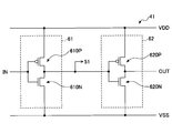
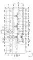
- FIG. 4 is a circuit diagram showing the configuration of the first drive buffer 41.
- FIG. 5 is a schematic view showing a planar configuration of an example of the first drive buffer 41.
- the first drive buffer 41 includes an inverter 61 and an inverter 62.
- the input signal IN is input to the inverter 61
- the output of the inverter 61 is input to the inverter 62
- the output signal OUT is output from the inverter 62.
- the inverter 61 includes a P-channel MOS transistor 610P and an N-channel MOS transistor 610N.
- the inverter 62 includes a P-channel MOS transistor 620P and an N-channel MOS transistor 620N.
- a power supply line 1110 corresponding to VDD wiring and a power supply line 1130 corresponding to VSS wiring are provided.
- Power lines 1110 and 1130 extend in the X direction.
- a semiconductor fin 651 extending in the X direction is provided on the power supply line 1130 side of the power supply line 1110.
- a semiconductor fin 652 extending in the X direction is provided on the power supply line 1130 side of the fin 651.
- a local wiring 631 is provided which is connected to the power supply line 1110 via the via 681, extends in the Y direction, and is connected to the fin 651.
- a local wiring 632 connected to the power line 1130 via the via 682, extending in the Y direction, and connected to the fin 652 is provided.
- Local wiring 634 connected to fins 651 and 652 is provided on the positive side in the X direction from the local wirings 631 and 632.
- Local wiring 636 connected to fins 651 and 652 is provided on the negative side in the X direction from the local wirings 631 and 632.
- a gate electrode 612 that intersects the fins 651 and 652 via a gate insulating film (not shown) is provided between the local wiring 631 and the local wiring 634, and between the local wiring 632 and the local wiring 634.
- a gate electrode 622 that intersects the fins 651 and 652 via a gate insulating film (not shown) is provided between the local wiring 631 and the local wiring 636, and between the local wiring 632 and the local wiring 636.
- the gate electrode 612 is connected to wiring 611 via local wiring 633 and via 641.
- the gate electrode 622 is connected to wire 692 via local wire 635 and via 643.
- the wiring 692 is also connected to the local wiring 634.
- the local wiring 636 is connected to the wiring 621 via the via 644.
- the input signal IN is input to the wiring 611, and the output signal OUT is output from the wiring 621 (see FIG. 4).
- Wiring 692 may be connected to the gate of the first switch transistor 51. Instead of wiring 692, either wiring 611 or wiring 621 may be connected to the gate of the first switch transistor 51. That is, the output of the inverter 61 may be input to the gate of the first switch transistor 51. Instead of the output of the inverter 61, either the input of the inverter 61 or the output of the inverter 62 may be connected to the gate of the first switch transistor 51.
- the second to fourth drive buffers 42 to 44 can have the same configuration as the first drive buffer 41.
- the configurations of the inverters 61 and 62 are examples.
- the number of pairs of P-channel MOS transistors and N-channel MOS transistors included in the inverters 61 and 62 may be two or more.
- FIG. 6 is a circuit diagram showing the configuration of the inverter.
- FIG. 7 is a schematic view showing a planar configuration of the inverter.
- the inverter 70 includes a P-channel MOS transistor 710P and an N-channel MOS transistor 710N.
- a power supply line 2120 corresponding to V VDD wiring and a power supply line 2130 corresponding to VVSS wiring are provided.
- Power lines 2120 and 2130 extend in the X direction.
- Semiconductor fins 751 extending in the X direction are provided on the power supply line 2130 side of the power supply line 2120.
- two fins 751 are provided.
- a semiconductor fin 752 extending in the X direction is provided on the power supply line 2130 side of the fin 751.
- two fins 752 are provided.
- a local wiring 731 that is connected to the power supply line 2120 via the via 781, extends in the Y direction, and is connected to the fin 751 is provided.
- a local wiring 732 connected to the power line 2130 via the via 782, extending in the Y direction, and connected to the fin 752 is provided.
- Local wiring 734 connected to fins 751 and 752 is provided on the positive side in the X direction from the local wirings 731 and 732.
- a circuit may be provided over an area where the power lines 2120 and 2130 are three or more. That is, a so-called multi-height circuit may be provided.
- a gate electrode 712 that intersects the fins 751 and 752 via a gate insulating film (not shown) is provided between the local wiring 731 and the local wiring 734, and between the local wiring 732 and the local wiring 734.
- the gate electrode 712 is connected to the wiring 711 via the local wiring 733 and the via 741.
- the local wiring 734 is connected to the wiring 760 via the via 742.
- the input signal IN is input to the wiring 711, and the output signal OUT is output from the wiring 760 (see FIG. 6).
- FIGS. 5 and 7 planar transistors, complementary field effect transistors (CFETs), and nanowires are used in logic circuits such as buffers. A transistor or the like using the above may be provided.
- V VDD wiring and the VVSS wiring are provided.
- VSS wiring may be provided instead of VVSS wiring.
- the combination of the third drive buffer 43 and the third switch transistor 53 may not be provided.
- VDD wiring may be provided instead of V VDD wiring.
- the combination of the first drive buffer 41 and the first switch transistor 51 may not be provided.
- the combination of the second drive buffer 42 and the second switch transistor 52 or the combination of the fourth drive buffer 44 and the fourth switch transistor 54 is provided, the other is provided. It does not have to be.
- the combination of the second drive buffer 42 and the second switch transistor 52 is provided, the combination of the fourth drive buffer 44 and the fourth switch transistor 54 may not be provided.
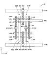
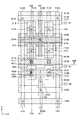
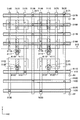
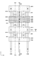
- FIG. 8 and 9 are schematic views showing a planar configuration of the semiconductor device according to the first embodiment.
- 10 and 11 are cross-sectional views showing a semiconductor device according to the first embodiment.
- FIG. 8 shows the internal configuration of the first chip 10 and the second chip 20
- FIG. 9 shows the internal configuration of the second chip 20.
- FIG. 10 corresponds to a cross-sectional view taken along the line Y11-Y21 in FIGS. 8 and 9, and
- FIG. 11 corresponds to a cross-sectional view taken along the line Y12-Y22 in FIGS. 8 and 9.
- the first chip 10 includes a control signal line 3110 extending in the X direction.
- the first chip 10 has a power supply line 2160 extending in the X direction and a power supply line 2170 extending in the X direction arranged on the positive side in the Y direction from the control signal line 3110. included.
- the power supply line 2160 is located closer to the control signal line 3110 than the power supply line 2170.
- the power supply line 2160 corresponds to the VSS wiring
- the power supply line 2170 corresponds to the VSS wiring.
- the control signal line 3110 is connected between the first drive buffer 41 and the gate of the first switch transistor 51.
- a plurality of sets of power supply lines 2160 and power supply lines 2170 may be arranged alternately.
- the power supply line 2160 and the power supply line 2170 are arranged in the second power domain 31B.
- the control signal line 3110 may also be arranged in the second power domain 31B.
- the first chip 10 has a control signal line 3120 extending in the X direction and a power supply line 1120 extending in the X direction arranged on the negative side in the Y direction with respect to the control signal line 3110. And the power supply line 1130 extending in the X direction.
- the control signal line 3120 is located closer to the control signal line 3110 than the power supply line 1120
- the power supply line 1120 is located closer to the control signal line 3110 than the power supply line 1130.
- the power supply line 1120 corresponds to the VDD wiring electrically connected to the second power supply pad 82
- the power supply line 1130 corresponds to the VSS wiring.
- the control signal line 3120 is connected between the second drive buffer 42 and the gate of the second switch transistor 52.
- the control signal line 3120, the power supply line 1120, and the power supply line 1130 are arranged outside the second power domain 31B.
- the arrangement of each control signal line and each power supply line is not limited to the example of FIG. 8, and may be changed as appropriate.
- a plurality of grooves extending in the X direction are formed on the substrate 11, and the control signal line 3110, the power supply line 2160, the power supply line 2170, the control signal line 3120, the power supply line 1120, and the power supply line are formed. 1130 is formed in these grooves.
- the power supply line 2160, power supply line 2170, power supply line 1120, and power supply line 1130 having such a structure may be referred to as BPR (Buried Power Rail).
- An element separation film (not shown) may be formed on the surface of the substrate 11.
- the device separation membrane is formed by, for example, the STI (Shallow Trench Isolation) method. The surface of the element separation membrane may or may not be flush with the surface of the substrate 11.
- a circuit such as a standard cell 56 is connected between the power supply line 2160 and the power supply line 2170 in the second power domain 31B.
- the first power domain 31A is arranged outside the second power domain 31B, and the power supply line 1120 and the power supply line 1130 are arranged in the first power domain 31A. Circuits such as the first drive buffer 41, the second drive buffer 42, and their control circuits are connected between the two.
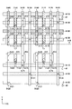
- the first wiring layer 12 includes control signal lines 3110, power supply lines 2160, power supply lines 2170, control signal lines 3120, power supply lines 1120, and control signal lines 4110 and 4120 arranged above the power supply lines 1130.
- the first wiring layer 12 is formed with vias 4111 that connect the control signal line 4110 and the control signal line 3110, and vias 4121 that connect the control signal line 4120 and the control signal line 3120.
- the via 4111 is formed below the control signal line 4110, and the via 4121 is formed below the control signal line 4120.
- Vias 1121, 1131, 2161, 2171, 3111 and 3121 are formed on the substrate 11 so as to penetrate the substrate 11 to the back surface.
- the via 1121 is formed below the power line 1120
- the via 1131 is formed below the power line 1130
- the via 2161 is formed below the power line 2160
- the via 2171 is formed below the power line 2170.
- the via 3111 is formed below the control signal line 3110
- the via 3121 is formed below the control signal line 3120.
- the second chip 20 is formed inside the insulating layer 25, the first sub-wiring layer 201 formed on the surface layer portion of the insulating layer 25, and the insulating layer 25. It has a second sub-wiring layer 202.
- the first sub-wiring layer 201 includes a power supply line 5120, a power supply line 5130, a power supply line 5160, a control signal line 7110, and a control signal line 7120.
- the power supply line 5120, the power supply line 5130, the power supply line 5160, the control signal line 7110, and the control signal line 7120 extend in the Y direction.
- the power supply line 5160 is located between the two control signal lines 7110
- the control signal line 7110 is between the power supply line 5130 and the power supply line 5160.
- the power supply line 5130 is formed from below the power supply lines 2160 and 2170 to below the power supply line 1130.
- the power supply line 5160 is formed in a region overlapping the second power domain 31B in a plan view.
- the power supply line 5120 is formed on an extension of the power supply line 5160 outside the region overlapping the second power domain 31B in a plan view.
- the power supply line 5120 corresponds to the VDD wiring electrically connected to the second power supply pad 82
- the power supply line 5130 corresponds to the VSS wiring
- the power supply line 5160 corresponds to the V VDD wiring.
- the second sub-wiring layer 202 includes a power supply line 6110, a power supply line 6120, and a power supply line 6160.
- the power supply line 6110, the power supply line 6120, and the power supply line 6160 extend in the X direction.
- the power supply line 6110 is located below the power supply line 2170
- the power supply line 6160 is located below the power supply line 6170.
- the power supply line 6120 has a portion that overlaps with the power supply line 5120 in a plan view.
- the insulating layer 25 is formed with vias 5121 connecting the power supply line 5120 and the power supply line 6120, and vias 5161 connecting the power supply line 5160 and the power supply line 6160.
- the power supply line 6110 corresponds to the VDD wiring electrically connected to the first power supply pad 81
- the power supply line 6120 corresponds to the VDD wiring electrically connected to the second power supply pad 82
- the power supply line corresponds to the power supply line.
- 6160 corresponds to V VDD wiring.
- the insulating layer 25 is formed with a plurality of semiconductor layers 213 that overlap with a pair of adjacent power supply lines 6110 and 6160 in a plan view in a region that overlaps with the second power domain 31B in a plan view.
- the semiconductor layer 213 is connected to the power supply lines 6110 and 6160.
- the gate insulating film 214 is formed on the semiconductor layer 213, and the gate electrode 215 is formed on the gate insulating film 214.
- the gate insulating film 214 is in contact with the semiconductor layer 213 and the gate electrode 215.
- the gate electrode 215 is located between the power supply line 6110 and the power supply line 6160 in a plan view.
- a via 7111 is formed on the insulating layer 25 to connect the control signal line 7110 and each gate electrode 215.
- the semiconductor layer 213, the gate insulating film 214, and the gate electrode 215 are included in the first switch transistor 51.
- the insulating layer 25 is formed with a plurality of semiconductor layers 223 that overlap with a pair of adjacent power supply lines 6110 and 6120 in a plan view.
- the semiconductor layer 223 may be arranged outside the region overlapping the second power domain 31B in a plan view, or may be arranged within the region.
- the semiconductor layer 223 is connected to the power supply lines 6110 and 6120.
- the gate insulating film 224 is formed on the semiconductor layer 223, and the gate electrode 225 is formed on the gate insulating film 224.
- the gate insulating film 224 is in contact with the semiconductor layer 223 and the gate electrode 225.
- the gate electrode 225 is located between the power supply line 6110 and the power supply line 6120 in a plan view.
- a via 7121 connecting the control signal line 7120 and each gate electrode 225 is formed on the insulating layer 25.
- the semiconductor layer 223, the gate insulating film 224, and the gate electrode 225 are included in the second switch transistor 52.
- the power potential of VDD and the power potential of VSS are supplied from the outside through a plurality of pads 23 provided on the back surface of the second chip 20. Further, the signal processed by the semiconductor device is output to the outside through the plurality of pads 23.
- the first switch transistor 51 is turned off when it is not necessary to operate the standard cell 56. That is, a control signal that makes the power supply line 6110 and the power supply line 6160 non-conducting is input to the gate electrode 215.
- the power supply line 6160 (V VDD wiring) is insulated from the first power supply pad 81 and the second power supply pad 82, and the power supply potential is supplied from the power supply line 6110 (VDD wiring) to the power supply line 6160 (V VDD wiring). It is blocked.
- the first switch transistor 51 is turned on after the second switch transistor 52 is turned off. That is, after a control signal for making the power supply line 6110 and the power supply line 6120 non-conducting is input to the gate electrode 225, the gate electrode 215 is controlled to make the power supply line 6110 and the power supply line 6160 conductive. The signal is input.
- the power supply line 6120 (VDD wiring) is insulated from the power supply line 6110 (VDD wiring), and the power supply line 6160 (V VDD wiring) is connected to the first power supply pad 81 via the power supply line 6110 (VDD wiring). It is electrically connected and the power supply potential of VDD is supplied to the power supply line 6160 (V VDD wiring).
- the standard cell 56 When the power supply potential of VDD is supplied to the power supply line 6160 (V VDD wiring), the standard cell 56 starts to operate. At this time, when the second switch transistor 52 is in the ON state, the power supply potential of VDD is also supplied to the second power domain 31B from the second power supply pad 82, and the power supply potential is suddenly supplied. Noise is generated, and this noise may extend to the first power domain 31A. Such a sudden supply of power potential is sometimes called a rush current. On the other hand, in the present embodiment, since the second switch transistor 52 is in the off state, the rush current is suppressed and the generation of noise is suppressed.
- the second switch transistor 52 After the standard cell 56 starts operating, when the fluctuation of the power potential of VDD supplied to the second power domain 31B settles down, the second switch transistor 52 is turned on. That is, a control signal for conducting between the power supply line 6110 and the power supply line 6120 is input to the gate electrode 225. As a result, a stable VDD power potential is supplied to the first power domain 31A and the second power domain 31B.
- FIG. 12 is a schematic view showing a planar configuration of the semiconductor device according to the first modification of the first embodiment.
- FIG. 12 mainly shows a portion different from the first embodiment of the first modification, and the illustration of the other portion is omitted.
- the power supply lines 6120 extending in the X direction are arranged on both the positive side in the Y direction and the negative side in the Y direction of the second power domain 31B in a plan view. There is. Then, outside the region that overlaps with the second power domain 31B in a plan view, a plurality of semiconductor layers 223 that overlap with a pair of power supply lines 6110 and 6120 adjacent to each other in the Y direction in a plan view are formed.
- a gate insulating film 224 (see FIG. 11) and a gate electrode 225 are formed on the semiconductor layer 223.
- the semiconductor layer 223, the gate insulating film 224, and the gate electrode 225 are included in the second switch transistor 52.
- a plurality of power supply lines 6110 extending in the X direction are arranged in a region overlapping with the second power domain 31B in a plan view.
- a power supply line 6120 extending in the X direction is arranged on an extension of these power supply lines 6110 on both the positive side in the X direction and the negative side in the X direction of the second power domain 31B in a plan view.
- a plurality of semiconductor layers 223 that overlap with a pair of power supply lines 6110 and 6120 adjacent to each other in the X direction in a plan view are formed.
- a gate insulating film 224 (see FIG. 11) and a gate electrode 225 are formed on the semiconductor layer 223.
- the semiconductor layer 223, the gate insulating film 224, and the gate electrode 225 are included in the second switch transistor 52.
- a power supply line 5120 extending in the Y direction is arranged on both the positive side in the X direction and the negative side in the X direction of the second power domain 31B in a plan view.
- the power supply line 5120 is orthogonal to a plurality of power supply lines 6120 in a plan view, and the power supply line 5120 and the power supply line 6120 orthogonal to the power supply line 5120 are connected via a via 5121.
- the via 7121, the control signal line 7120, and the like are not shown. That is, vias 7121, control signal lines 7120, and the like are arranged in each of the second switch transistors 52. Further, although not shown in FIG. 12, the first switch transistor 51 is connected between the power supply lines 6110 and the power supply lines 6160 that are adjacent to each other in the Y direction.
- the second switch transistor 52 does not have to be arranged on all of the positive side in the X direction, the negative side in the X direction, the positive side in the Y direction, and the negative side in the Y direction of the second power domain 31B.
- the second switch transistor 52 may be arranged only on the positive side in the X direction and the negative side in the X direction of the second power domain 31B.
- the second switch transistor 52 may be arranged only on the positive side in the Y direction and the negative side in the Y direction of the second power domain 31B.
- a part of the power supply lines 6110 and 6120 may not be directly connected to the second switch transistor 52, or may be connected to the second switch transistor 52 via other wiring.
- FIG. 13 is a schematic view showing a planar configuration of the semiconductor device according to the second modification of the first embodiment.
- FIG. 13 mainly shows a portion different from the first embodiment of the second modification, and the illustration of the other portion is omitted.
- the ends of the plurality of power supply lines 6110 on the positive side in the X direction in the first modification are connected to each other, and the plurality of power supply lines in the first modification are connected to each other.
- the ends of the 6110 on the negative side in the X direction are connected to each other. That is, the power supply line 6110 has a ladder-like planar shape.
- the power supply line 6110 has an annular portion and a portion extending in the X direction inside the annular portion and connecting to the annular portion in a plan view. Further, an annular power supply line 6120 is arranged outside the annular portion of the power supply line 6110 in a plan view.
- the semiconductor layer 223 that overlaps a part of the power supply lines 6110 and a part of the 6120 adjacent to each other in the Y direction in a plan view is formed so as to extend in the X direction.
- a gate insulating film 224 (see FIG. 11) extending in the X direction and a gate electrode 225 are formed on the semiconductor layer 223.
- the semiconductor layer 223, the gate insulating film 224, and the gate electrode 225 are included in the second switch transistor 52.
- the semiconductor layer 223 that overlaps with a part of the power supply lines 6110 and a part of the 6120 adjacent to each other in the X direction in a plan view is formed so as to extend in the Y direction.
- a gate insulating film 224 (see FIG. 11) extending in the Y direction and a gate electrode 225 are formed on the semiconductor layer 223.
- the semiconductor layer 223, the gate insulating film 224, and the gate electrode 225 are included in the second switch transistor 52.
- the via 7121, the control signal line 7120, and the like are not shown. That is, vias 7121, control signal lines 7120, and the like are arranged in each of the second switch transistors 52. Further, although not shown in FIG. 13, the first switch transistor 51 is connected between the power supply lines 6110 and the power supply lines 6160 that are adjacent to each other in the Y direction.
- the power supply line 6110 does not have an annular portion, but has a portion extending in the X direction and a portion extending in the Y direction, and a semiconductor layer 223 extending in the X direction and a portion extending in the Y direction.
- An extending semiconductor layer 223 may be arranged.
- the power supply line 6120 does not have an annular planar shape, but has a portion extending in the X direction and a portion extending in the Y direction, and the semiconductor layer 223 extending in the X direction and the Y direction.
- the semiconductor layer 223 extending to the surface may be arranged.
- the semiconductor layer 213, the gate insulating film 214, and the gate electrode 215 included in the first switch transistor 51 may extend in the X direction.
- FIG. 14 is a cross-sectional view showing a semiconductor device according to a third modification of the first embodiment.
- FIG. 14 mainly shows a part different from the first embodiment of the third modification, and the illustration of the other part is omitted.
- the second wiring layer 22 further includes the third sub wiring layer 203 below the second sub wiring layer 202. That is, the third sub-wiring layer 203 is formed so as to be separated from the first chip 10 by the second sub-wiring layer 202.
- the third sub-wiring layer 203 includes, for example, a power supply line 8110 and a power supply line 8120.
- the power supply line 8110 and the power supply line 8120 extend in the Y direction.
- the power supply line 8110 has a portion that overlaps with the power supply line 6110 in a plan view.
- the power supply line 8120 has a portion that overlaps with the power supply line 8120 in a plan view.
- the insulating layer 25 is formed with vias 6111 for connecting the power supply line 6110 and the power supply line 8110, and vias 6121 for connecting the power supply line 6120 and the power supply line 8120.
- the power supply line 8110 corresponds to the VDD wiring electrically connected to the first power supply pad 81
- the power supply line 8120 corresponds to the VDD wiring electrically connected to the second power supply pad 82.
- the insulating layer 25 is formed with a plurality of semiconductor layers 233 that overlap with a pair of adjacent power supply lines 8110 and 8120 in a plan view outside the region that overlaps with the second power domain 31B in a plan view.
- the semiconductor layer 233 is connected to the power supply lines 8110 and 8120.
- the gate insulating film 234 is formed on the semiconductor layer 233, and the gate electrode 235 is formed on the gate insulating film 234.
- the gate insulating film 234 is in contact with the semiconductor layer 233 and the gate electrode 235.
- the gate electrode 235 is located between the power supply line 8110 and the power supply line 8120 in a plan view.
- a via or the like (not shown) connecting the control signal line 7120 and the gate electrode 235 is formed on the insulating layer 25.
- the semiconductor layer 233, the gate insulating film 234, and the gate electrode 235 are included in the second switch transistor 52.
- the same effect as that of the first embodiment can be obtained by the third modification.
- the power supply potential can be more stabilized.
- the semiconductor layer 233, the gate insulating film 234, and the gate electrode 235 may not be provided.
- FIG. 15 is a circuit diagram showing a configuration of an example of a circuit included in the semiconductor device according to the fourth modification of the first embodiment.
- FIG. 15 mainly shows a portion different from the first embodiment of the fourth modification, and the illustration of the other portion is omitted.
- the second wiring layer 22 includes the first sub-wiring layer 201 and the second sub-wiring layer 202.
- the first switch transistor 51 and the third switch transistor 53 are arranged on the first sub-wiring layer 201.
- the second switch transistor 52 and the fourth switch transistor 54 are arranged in both the first sub-wiring layer 201 and the second sub-wiring layer 202.
- FIG. 16 shows the internal configuration of the first chip 10 and the second chip 20
- FIG. 17 shows the internal configuration of the second chip 20.
- 16 and 17 mainly show parts different from the first embodiment of the fifth modification, and the illustration of other parts will be omitted.
- the second sub-wiring layer 202 has a power supply line 6130 extending in the X direction.
- the power supply line 6130 corresponds to VSS wiring.
- the power supply line 6130 is orthogonal to the power supply line 5130 in a plan view, and the power supply line 5130 and the power supply line 6130 orthogonal to the power supply line 5130 are connected via a via 5131.
- the first sub-wiring layer 201 has a power supply line 5170 extending in the Y direction.
- the power supply line 5170 corresponds to a VDD wiring electrically connected to the first power supply pad 81.
- the power supply line 5170 is orthogonal to the power supply line 6110, and the power supply line 5170 and the power supply line 6110 orthogonal to the power supply line 5170 are connected via a via 5171.
- the control signal line 7110 is arranged between the power supply line 5160 and the power supply line 5170 in the area overlapping the second power domain 31B in a plan view.
- the semiconductor layer 213 is formed above the power supply line 6130 so as to overlap the power supply line 5160, the control signal line 7110, and the power supply line 5170 in a plan view.
- a gate insulating film 214 (see FIG. 11) and a gate electrode 215 are formed on the semiconductor layer 213.
- the gate electrode 215 is connected to the control signal line 7110 via the via 7111.
- the semiconductor layer 213 is connected to the power supply line 5160 on the negative side in the X direction from the gate electrode 215 via the via 5162, and is connected to the power supply line 5170 on the positive side in the X direction from the gate electrode 215 via the via 5172. ing.
- the via 5162 is formed below the power line 5160, and the via 5172 is formed below the power line 5170.
- a control signal line 7120 is arranged between the power supply line 5120 and the power supply line 5170 outside the region that overlaps with the second power domain 31B in a plan view.
- the semiconductor layer 223 is formed so as to overlap the power supply line 5120, the control signal line 7120, and the power supply line 5170 in a plan view.
- a gate insulating film 224 (see FIG. 11) and a gate electrode 225 are formed on the semiconductor layer 223.
- the gate electrode 225 is connected to the control signal line 7120 via the via 7121.
- the semiconductor layer 223 is connected to the power supply line 5120 on the negative side in the X direction from the gate electrode 225 via the via 5123, and is connected to the power supply line 5170 on the positive side in the X direction from the gate electrode 225 via the via 5173. ing.
- the via 5123 is formed below the power line 5120, and the via 5173 is formed below the power line 5170.
- first switch transistor 51 and the second switch transistor 52 may also be formed on the second sub-wiring layer 202.
- FIG. 18 is a schematic view showing a planar configuration of a semiconductor device according to a sixth modification of the first embodiment.
- FIG. 18 mainly shows a portion different from the first embodiment of the sixth modification, and the illustration of the other portion is omitted.
- the semiconductor device according to the sixth modification is provided with a fourth switch transistor 54 in addition to the first switch transistor 51 and the second switch transistor 52.
- the power supply lines 6220 extending in the X direction are arranged on both the positive side in the Y direction and the negative side in the Y direction of the second power domain 31B in a plan view. There is. Further, a plurality of power supply lines 6210 extending in the X direction are arranged in a region overlapping the second power domain 31B in a plan view. The power lines 6210 and 6220 are included in the second sub-wiring layer 202.
- the power supply line 6210 corresponds to the VSS wiring electrically connected to the third power supply pad 83
- the power supply line 6220 corresponds to the VSS wiring electrically connected to the fourth power supply pad 84.
- a plurality of semiconductor layers 243 that overlap with a pair of power supply lines 6210 and 6220 adjacent to each other in the Y direction in a plan view are formed outside the region that overlaps with the second power domain 31B in a plan view.
- a gate insulating film (not shown) and a gate electrode 245 are formed on the semiconductor layer 243.
- the semiconductor layer 243, the gate insulating film (not shown), and the gate electrode 245 are included in the fourth switch transistor 54.
- the first sub-wiring layer 201 has a power supply line 5220 extending in the Y direction.
- the power supply line 5220 corresponds to VSS wiring.
- the power supply line 5220 is orthogonal to a plurality of power supply lines 6210 in a plan view, and the power supply line 5220 and the power supply line 6210 orthogonal to the power supply line 5220 are connected via a via 5221.
- the via 7121, the control signal line 7120, and the like are not shown. That is, vias 7121, control signal lines 7120, and the like are arranged in each of the second switch transistors 52.
- the fourth switch transistor 54 of FIG. 18 the vias and control signal lines connected to the gate electrode 245 are not shown. That is, vias, control signal lines, and the like are arranged in each of the fourth switch transistors 54.
- the first switch transistor 51 is connected between the power supply lines 6110 and the power supply lines 6160 that are adjacent to each other in the Y direction.
- the first switch transistor 51 is turned off when it is not necessary to operate the standard cell 56.
- the power supply line 6160 (V VDD wiring) is insulated from the first power supply pad 81 and the second power supply pad 82, and the power supply potential is supplied from the power supply line 6110 (VDD wiring) to the power supply line 6160 (V VDD wiring). It is blocked (see FIGS. 8 to 11).
- the first switch transistor 51 is turned on after the second switch transistor 52 and the fourth switch transistor 54 are turned off. That is, a control signal that makes the power supply line 6110 and the power supply line 6120 non-conducting is input to the gate electrode 225, and a control signal that makes the power supply line 6210 and the power supply line 6220 non-conducting is input to the gate electrode 245. Is input, a control signal for conducting between the power supply line 6110 and the power supply line 6160 is input to the gate electrode 215.
- the power supply line 6120 (VDD wiring) is insulated from the power supply line 6110 (VDD wiring), and the power supply line 6220 (VSS wiring) is insulated from the power supply line 6210 (VSS wiring), and then the power supply line 6160 (V VDD wiring).
- the power supply potential of VDD is supplied to the wiring).
- the second switch transistor 52 and the fourth switch transistor 54 are turned on. That is, a control signal for conducting between the power supply line 6110 and the power supply line 6120 is input to the gate electrode 225, and a control signal for conducting between the power supply line 6210 and the power supply line 6220 is input to the gate electrode 245. Will be done. As a result, a stable VDD power potential is supplied to the first power domain 31A and the second power domain 31B.
- a fourth switch transistor 54 may be provided in addition to the second switch transistor 52. If the fourth switch transistor 54 is provided, the second switch transistor 52 may not be provided.
- a third switch transistor 53 may be provided in addition to the first switch transistor 51. If the third switch transistor 53 is provided, the first switch transistor 51 may not be provided.
- the second embodiment differs from the first embodiment mainly in the arrangement of the switch transistors.
- 19 and 20 are schematic views showing a planar configuration of the semiconductor device according to the second embodiment.
- 21 and 22 are cross-sectional views showing a semiconductor device according to the second embodiment.
- FIG. 19 mainly shows the power supply line on the upper layer side
- FIG. 20 mainly shows the power supply line on the lower layer side.
- 21 corresponds to a cross-sectional view taken along the line Y13-Y23 in FIGS. 19 and 20
- FIG. 22 corresponds to a cross-sectional view taken along the line Y14-Y24 in FIGS. 19 and 20.
- the semiconductor device according to the second embodiment is composed of a single chip 30.
- the chip 30 has a substrate 31 and a wiring layer 36 on the substrate 31.
- the wiring layer 36 includes an insulating layer 35 and a plurality of power supply lines and vias formed in the insulating layer 35.
- the chip 30 includes a power supply line 2160 extending in the X direction and a power supply line 2170 extending in the X direction.
- the power supply line 2160 corresponds to the VSS wiring
- the power supply line 2170 corresponds to the VSS wiring.
- a plurality of sets of power supply lines 2160 and power supply lines 2170 may be arranged alternately.
- the power supply line 2160 and the power supply line 2170 are arranged in the second power domain 31B.
- the chip 30 includes a power supply line 1120 extending in the X direction and a power supply line 1130 extending in the X direction, which are arranged on the negative side in the Y direction with respect to the power supply lines 2160 and 2170.
- the power supply line 1120 is located closer to the power supply line 2170 than the power supply line 1130.
- the power supply line 1120 corresponds to the VDD wiring electrically connected to the second power supply pad 82
- the power supply line 1130 corresponds to the VSS wiring.
- a plurality of grooves extending in the X direction are formed on the substrate 31, and the power supply line 2160, the power supply line 2170, the power supply line 1120, and the power supply line 1130 are formed in these grooves. There is.
- a circuit such as a standard cell 56 is connected between the power supply line 2160 and the power supply line 2170 in the second power domain 31B.
- the first power domain 31A is arranged outside the second power domain 31B, and the power supply line 1120 and the power supply line 1130 are arranged in the first power domain 31A. Circuits such as the first drive buffer 41, the second drive buffer 42, and their control circuits are connected between the two.
- the wiring layer 36 includes a control signal line 7310, a control signal line 7320, a power supply line 5320, a power supply line 5330, and a power supply line 5360.
- the control signal line 7310, the control signal line 7320, the power supply line 5320, the power supply line 5330, and the power supply line 5360 extend in the Y direction.
- the power supply line 5320 is orthogonal to the power supply line 1120 in plan view
- the power supply line 5330 is orthogonal to the power supply line 1130 or 2170 in plan view
- the power supply line 5360 is orthogonal to the power supply line 216 in plan view.
- the insulating layer 35 is formed with vias 1321 for connecting the power supply line 5320 and the power supply line 1120, and vias 1331 for connecting the power supply line 5330 and the power supply line 1130.
- the insulating layer 35 is formed with vias 2371 that connect the power supply line 5330 and the power supply line 2170, and vias 2361 that connect the power supply line 5360 and the power supply line 2160.
- the control signal lines 7310 and 7320 are orthogonal to the power supply lines 2160 and 2170 in plan view.
- the power supply line 6310 is formed above the power supply line 2170, and the power supply line 6360 is formed above the power supply line 2160.
- the power lines 6310 and 6360 extend in the X direction.
- a plurality of semiconductor layers 273 that overlap with a pair of adjacent power supply lines 6310 and 6360 in a plan view are formed in a region that overlaps with the second power domain 31B in a plan view.
- a gate insulating film 274 is formed under the semiconductor layer 273, and a gate electrode 275 is formed under the gate insulating film 274. The gate insulating film 274 is in contact with the semiconductor layer 273 and the gate electrode 275.
- the gate electrode 275 is located between the power supply line 6310 and the power supply line 6360 in a plan view.
- the insulating layer 35 has a via 6313 that connects the semiconductor layer 273 and the power supply line 6310, a via 6363 that connects the semiconductor layer 273 and the power supply line 6360, and a via that connects the control signal line 7310 and each gate electrode 275. 7311 and are formed.
- the semiconductor layer 273, the gate insulating film 274, and the gate electrode 275 are included in the first switch transistor 51.
- a power supply line 6320 is formed in the same sub-wiring layer as the power supply lines 6310 and 6360 between the power supply line 1120 and the power supply line 2170 in a plan view.
- the power line 6320 extends in the X direction.
- the insulating layer 35 is formed with a plurality of semiconductor layers 283 that overlap with a pair of adjacent power supply lines 6310 and 6320 in a plan view outside the region that overlaps with the second power domain 31B in a plan view.
- a gate insulating film 284 is formed under the semiconductor layer 283, and a gate electrode 285 is formed under the gate insulating film 284. The gate insulating film 284 is in contact with the semiconductor layer 283 and the gate electrode 285.
- the gate electrode 285 is located between the power supply line 6310 and the power supply line 6320 in a plan view.
- the insulating layer 35 has a via 6313 connecting the semiconductor layer 283 and the power supply line 6310, a via 6323 connecting the semiconductor layer 283 and the power supply line 6320, and a via connecting the control signal line 7320 and each gate electrode 285. 7321 and is formed.
- the semiconductor layer 283, the gate insulating film 284, and the gate electrode 285 are included in the second switch transistor 52.
- a power supply line 4360 extending in the Y direction is formed between the power supply line 5360 and the power supply line 6360.
- the insulating layer 35 is formed with vias 4361 that connect the power supply line 6360 and the power supply line 4360, and vias 5361 that connect the power supply line 4360 and the power supply line 5360.
- a power supply line 4320 extending in the Y direction is formed between the power supply line 5320 and the power supply line 6320.
- the insulating layer 35 is formed with vias 4321 that connect the power supply line 6320 and the power supply line 4320, and vias 5321 that connect the power supply line 4320 and the power supply line 5320.
- a power supply line 4330 extending in the Y direction is formed above a plurality of power supply lines 5330 arranged in the Y direction.
- the power supply line 4330 is formed in the same sub-wiring layer as, for example, the power supply lines 4320 and 4360.
- a via 5331 connecting the power supply line 4330 and the power supply line 5330 is formed on the insulating layer 35.
- a power supply line 8310 extending in the Y direction may be formed above the power supply lines 6310 and 6360, and a via connecting the power supply line 8310 and the power supply line 6310. 6311 may be formed. Further, the power supply line 8320 may be formed above the power supply line 6320, or a via 6321 connecting the power supply line 8320 and the power supply line 6320 may be formed.
- the first switch transistor 51 is turned on after the second switch transistor 52 is turned off. That is, after a control signal for making the power supply line 6310 and the power supply line 6320 non-conducting is input to the gate electrode 285, the gate electrode 275 is controlled to make the power supply line 6310 and the power supply line 6360 conductive. The signal is input.
- the second switch transistor 52 is turned on. That is, a control signal for conducting between the power supply line 6310 and the power supply line 6320 is input to the gate electrode 285. As a result, a stable VDD power potential is supplied to the first power domain 31A and the second power domain 31B.
- 23 to 25 are cross-sectional views showing an example of the cross-sectional configuration of the switch transistor.
- the underlying insulating film 102 is provided in the insulating layer 101, and the semiconductor layer 103, the gate insulating film 104, and the gate electrode 105 are provided on the underlying insulating film 102.
- a control signal line 110, a power supply line 120 corresponding to VDD wiring, and a power supply line 130 corresponding to V VDD wiring are provided on the surface layer portion of the insulating layer 101.
- the semiconductor layer 103 has a channel 103C and a source 103S and a drain 103D sandwiching the channel 103C.
- the power supply line 120 and the source 103S are connected via the via 121, and the power supply line 130 and the drain 103D are connected via the via 131.
- a power supply line 123 corresponding to VDD wiring and a power supply line 133 corresponding to V VDD wiring are provided under the underlying insulating film 102.
- the power supply line 120 and the power supply line 123 are connected via the via 122, and the power supply line 130 and the power supply line 133 are connected via the via 132.
- the control signal line 110 is connected to the gate electrode 105 via the via 111.
- the gate insulating film 204 is provided on the underlying insulating film 102, the semiconductor layer 103 is provided on the gate insulating film 204, and the gate electrode 205 is provided under the gate insulating film 204.
- Other configurations are the same as in the first example.
- the power supply line 123 is provided so as to be connected to the lower surface of the source 103S of the semiconductor layer 103, and the power supply line 133 is provided so as to be connected to the lower surface of the drain 103D of the semiconductor layer 103.
- the power supply line 120 is connected to the power supply line 123 via the via 121, and the power supply line 130 is connected to the power supply line 133 via the via 131.
- Other configurations are the same as in the first example.
- the material of the underlying insulating film is, for example, silicon oxide, silicon nitride, silicon carbide, silicon oxide nitride, silicon oxide carbide, or the like.
- the material of the semiconductor layer is, for example, InGaZnO (IGZO), ZnO, ZnSnO, InZnO, or the like.
- the material of the gate insulating film is, for example, SiO 2 , SiO x N y , SiN, Al 2 O 3 and the like.
- the material of the gate electrode is, for example, a metal such as molybdenum, titanium, chromium, tantalum, magnesium, silver, tungsten, aluminum, copper, neodymium, ruthenium, scandium and the like.
- the material of the gate electrode may be graphene or the like.
- the first to fourth switch transistors 51 to 54 provided in the first embodiment, the first to fourth modified examples of the first embodiment, and the sixth modified example of the first embodiment are , Is classified into the third example.
- the first to fourth switch transistors 51 to 54 provided in the fifth modification of the first embodiment are classified into the first example.
- the first to fourth switch transistors 51 to 54 provided in the second embodiment are classified into the second example.
- the present invention has been described above based on each embodiment, the present invention is not limited to the requirements shown in the above embodiments. With respect to these points, the gist of the present invention can be changed without impairing the gist of the present invention, and can be appropriately determined according to the application form thereof.
- First chip 20 Second chip 31A, 31B: Power domain 41, 42, 43, 44: Drive buffer 51, 52, 53, 54: Switch transistor 56: Standard cell
Landscapes
- Physics & Mathematics (AREA)
- Condensed Matter Physics & Semiconductors (AREA)
- General Physics & Mathematics (AREA)
- Engineering & Computer Science (AREA)
- Computer Hardware Design (AREA)
- Microelectronics & Electronic Packaging (AREA)
- Power Engineering (AREA)
- Geometry (AREA)
- Semiconductor Integrated Circuits (AREA)
- Design And Manufacture Of Integrated Circuits (AREA)
- Internal Circuitry In Semiconductor Integrated Circuit Devices (AREA)
- Metal-Oxide And Bipolar Metal-Oxide Semiconductor Integrated Circuits (AREA)
Priority Applications (6)
| Application Number | Priority Date | Filing Date | Title |
|---|---|---|---|
| CN201980102690.2A CN114762113B (zh) | 2019-12-05 | 2019-12-05 | 半导体装置 |
| JP2021562407A JP7363921B2 (ja) | 2019-12-05 | 2019-12-05 | 半導体装置 |
| PCT/JP2019/047688 WO2021111604A1 (ja) | 2019-12-05 | 2019-12-05 | 半導体装置 |
| US17/829,341 US12284828B2 (en) | 2019-12-05 | 2022-05-31 | Semiconductor device |
| JP2023171195A JP7639871B2 (ja) | 2019-12-05 | 2023-10-02 | 半導体装置 |
| US19/089,996 US20250227996A1 (en) | 2019-12-05 | 2025-03-25 | Semiconductor device |
Applications Claiming Priority (1)
| Application Number | Priority Date | Filing Date | Title |
|---|---|---|---|
| PCT/JP2019/047688 WO2021111604A1 (ja) | 2019-12-05 | 2019-12-05 | 半導体装置 |
Related Child Applications (1)
| Application Number | Title | Priority Date | Filing Date |
|---|---|---|---|
| US17/829,341 Continuation US12284828B2 (en) | 2019-12-05 | 2022-05-31 | Semiconductor device |
Publications (1)
| Publication Number | Publication Date |
|---|---|
| WO2021111604A1 true WO2021111604A1 (ja) | 2021-06-10 |
Family
ID=76221141
Family Applications (1)
| Application Number | Title | Priority Date | Filing Date |
|---|---|---|---|
| PCT/JP2019/047688 Ceased WO2021111604A1 (ja) | 2019-12-05 | 2019-12-05 | 半導体装置 |
Country Status (4)
| Country | Link |
|---|---|
| US (2) | US12284828B2 (enExample) |
| JP (2) | JP7363921B2 (enExample) |
| CN (1) | CN114762113B (enExample) |
| WO (1) | WO2021111604A1 (enExample) |
Cited By (6)
| Publication number | Priority date | Publication date | Assignee | Title |
|---|---|---|---|---|
| WO2023053203A1 (ja) * | 2021-09-28 | 2023-04-06 | 株式会社ソシオネクスト | 半導体集積回路装置 |
| WO2023095616A1 (ja) * | 2021-11-29 | 2023-06-01 | 株式会社ソシオネクスト | 半導体集積回路装置 |
| TWI834467B (zh) * | 2022-06-28 | 2024-03-01 | 台灣積體電路製造股份有限公司 | 積體電路裝置及製造方法 |
| WO2024214205A1 (ja) * | 2023-04-12 | 2024-10-17 | 株式会社ソシオネクスト | 半導体装置 |
| WO2024214206A1 (ja) * | 2023-04-12 | 2024-10-17 | 株式会社ソシオネクスト | 半導体装置 |
| WO2024252660A1 (ja) * | 2023-06-09 | 2024-12-12 | 株式会社ソシオネクスト | 半導体装置 |
Citations (9)
| Publication number | Priority date | Publication date | Assignee | Title |
|---|---|---|---|---|
| JPS5326689A (en) * | 1976-08-25 | 1978-03-11 | Hitachi Ltd | Semiconductor integrated circuit unit |
| JPH05206420A (ja) * | 1992-01-30 | 1993-08-13 | Nec Ic Microcomput Syst Ltd | 半導体集積回路 |
| JPH11102910A (ja) * | 1997-09-29 | 1999-04-13 | Hitachi Ltd | 半導体集積回路 |
| JP2009302198A (ja) * | 2008-06-11 | 2009-12-24 | Elpida Memory Inc | 半導体チップ、半導体チップ群および半導体装置 |
| JP2011159810A (ja) * | 2010-02-01 | 2011-08-18 | Renesas Electronics Corp | 半導体集積回路及びその制御方法 |
| JP2012044042A (ja) * | 2010-08-20 | 2012-03-01 | Kawasaki Microelectronics Inc | 半導体集積回路および半導体集積回路装置 |
| JP2014165358A (ja) * | 2013-02-26 | 2014-09-08 | Panasonic Corp | 半導体装置及びその製造方法 |
| US20150187642A1 (en) * | 2013-12-30 | 2015-07-02 | International Business Machines Corporation | Double-sided segmented line architecture in 3d integration |
| WO2019194007A1 (ja) * | 2018-04-05 | 2019-10-10 | 株式会社ソシオネクスト | 半導体集積回路装置 |
Family Cites Families (13)
| Publication number | Priority date | Publication date | Assignee | Title |
|---|---|---|---|---|
| JP2009177200A (ja) * | 1998-05-01 | 2009-08-06 | Sony Corp | 半導体記憶装置 |
| JP2000223575A (ja) * | 1999-01-28 | 2000-08-11 | Hitachi Ltd | 半導体装置の設計方法、半導体装置および半導体装置の製造方法 |
| JP2009124667A (ja) * | 2007-01-25 | 2009-06-04 | Panasonic Corp | 双方向スイッチ及びその駆動方法 |
| JP4962173B2 (ja) * | 2007-07-02 | 2012-06-27 | ソニー株式会社 | 半導体集積回路 |
| US8530273B2 (en) | 2010-09-29 | 2013-09-10 | Guardian Industries Corp. | Method of making oxide thin film transistor array |
| DE102013207324A1 (de) | 2012-05-11 | 2013-11-14 | Semiconductor Energy Laboratory Co., Ltd. | Halbleitervorrichtung und elektronisches Gerät |
| EP2884542A3 (en) | 2013-12-10 | 2015-09-02 | IMEC vzw | Integrated circuit device with power gating switch in back end of line |
| DE112015006942T5 (de) * | 2015-09-25 | 2018-06-14 | Intel Corporation | Beidseitige Metallisierung mit einer durch das Silizium verteilten Stromversorgung |
| US9754923B1 (en) | 2016-05-09 | 2017-09-05 | Qualcomm Incorporated | Power gate placement techniques in three-dimensional (3D) integrated circuits (ICs) (3DICs) |
| EP3324436B1 (en) | 2016-11-21 | 2020-08-05 | IMEC vzw | An integrated circuit chip with power delivery network on the backside of the chip |
| JP6825476B2 (ja) * | 2017-04-28 | 2021-02-03 | 株式会社ソシオネクスト | 半導体装置 |
| US10950546B1 (en) | 2019-09-17 | 2021-03-16 | Taiwan Semiconductor Manufacturing Co., Ltd. | Semiconductor device including back side power supply circuit |
| US11004789B2 (en) | 2019-09-30 | 2021-05-11 | Taiwan Semiconductor Manufacturing Co., Ltd. | Semiconductor device including back side power supply circuit |
-
2019
- 2019-12-05 JP JP2021562407A patent/JP7363921B2/ja active Active
- 2019-12-05 CN CN201980102690.2A patent/CN114762113B/zh active Active
- 2019-12-05 WO PCT/JP2019/047688 patent/WO2021111604A1/ja not_active Ceased
-
2022
- 2022-05-31 US US17/829,341 patent/US12284828B2/en active Active
-
2023
- 2023-10-02 JP JP2023171195A patent/JP7639871B2/ja active Active
-
2025
- 2025-03-25 US US19/089,996 patent/US20250227996A1/en active Pending
Patent Citations (9)
| Publication number | Priority date | Publication date | Assignee | Title |
|---|---|---|---|---|
| JPS5326689A (en) * | 1976-08-25 | 1978-03-11 | Hitachi Ltd | Semiconductor integrated circuit unit |
| JPH05206420A (ja) * | 1992-01-30 | 1993-08-13 | Nec Ic Microcomput Syst Ltd | 半導体集積回路 |
| JPH11102910A (ja) * | 1997-09-29 | 1999-04-13 | Hitachi Ltd | 半導体集積回路 |
| JP2009302198A (ja) * | 2008-06-11 | 2009-12-24 | Elpida Memory Inc | 半導体チップ、半導体チップ群および半導体装置 |
| JP2011159810A (ja) * | 2010-02-01 | 2011-08-18 | Renesas Electronics Corp | 半導体集積回路及びその制御方法 |
| JP2012044042A (ja) * | 2010-08-20 | 2012-03-01 | Kawasaki Microelectronics Inc | 半導体集積回路および半導体集積回路装置 |
| JP2014165358A (ja) * | 2013-02-26 | 2014-09-08 | Panasonic Corp | 半導体装置及びその製造方法 |
| US20150187642A1 (en) * | 2013-12-30 | 2015-07-02 | International Business Machines Corporation | Double-sided segmented line architecture in 3d integration |
| WO2019194007A1 (ja) * | 2018-04-05 | 2019-10-10 | 株式会社ソシオネクスト | 半導体集積回路装置 |
Cited By (7)
| Publication number | Priority date | Publication date | Assignee | Title |
|---|---|---|---|---|
| WO2023053203A1 (ja) * | 2021-09-28 | 2023-04-06 | 株式会社ソシオネクスト | 半導体集積回路装置 |
| JPWO2023053203A1 (enExample) * | 2021-09-28 | 2023-04-06 | ||
| WO2023095616A1 (ja) * | 2021-11-29 | 2023-06-01 | 株式会社ソシオネクスト | 半導体集積回路装置 |
| TWI834467B (zh) * | 2022-06-28 | 2024-03-01 | 台灣積體電路製造股份有限公司 | 積體電路裝置及製造方法 |
| WO2024214205A1 (ja) * | 2023-04-12 | 2024-10-17 | 株式会社ソシオネクスト | 半導体装置 |
| WO2024214206A1 (ja) * | 2023-04-12 | 2024-10-17 | 株式会社ソシオネクスト | 半導体装置 |
| WO2024252660A1 (ja) * | 2023-06-09 | 2024-12-12 | 株式会社ソシオネクスト | 半導体装置 |
Also Published As
| Publication number | Publication date |
|---|---|
| US20220293634A1 (en) | 2022-09-15 |
| JP7363921B2 (ja) | 2023-10-18 |
| JPWO2021111604A1 (enExample) | 2021-06-10 |
| US20250227996A1 (en) | 2025-07-10 |
| JP7639871B2 (ja) | 2025-03-05 |
| US12284828B2 (en) | 2025-04-22 |
| CN114762113A (zh) | 2022-07-15 |
| CN114762113B (zh) | 2024-11-01 |
| JP2023171884A (ja) | 2023-12-05 |
Similar Documents
| Publication | Publication Date | Title |
|---|---|---|
| JP7315016B2 (ja) | 半導体装置 | |
| JP7639871B2 (ja) | 半導体装置 | |
| JP7529121B2 (ja) | 半導体装置 | |
| US12087735B2 (en) | Semiconductor device | |
| CN108807367B (zh) | 半导体装置 | |
| US12295168B2 (en) | Semiconductor device | |
| US12184282B2 (en) | Semiconductor device | |
| CN110634860B (zh) | 半导体装置 | |
| CN110326099B (zh) | 半导体集成电路装置 |
Legal Events
| Date | Code | Title | Description |
|---|---|---|---|
| 121 | Ep: the epo has been informed by wipo that ep was designated in this application |
Ref document number: 19954938 Country of ref document: EP Kind code of ref document: A1 |
|
| ENP | Entry into the national phase |
Ref document number: 2021562407 Country of ref document: JP Kind code of ref document: A |
|
| NENP | Non-entry into the national phase |
Ref country code: DE |
|
| 122 | Ep: pct application non-entry in european phase |
Ref document number: 19954938 Country of ref document: EP Kind code of ref document: A1 |