WO2021085187A1 - 有機デバイス、その製造方法、表示装置、光電変換装置、電子機器、照明装置および移動体 - Google Patents
有機デバイス、その製造方法、表示装置、光電変換装置、電子機器、照明装置および移動体 Download PDFInfo
- Publication number
- WO2021085187A1 WO2021085187A1 PCT/JP2020/039132 JP2020039132W WO2021085187A1 WO 2021085187 A1 WO2021085187 A1 WO 2021085187A1 JP 2020039132 W JP2020039132 W JP 2020039132W WO 2021085187 A1 WO2021085187 A1 WO 2021085187A1
- Authority
- WO
- WIPO (PCT)
- Prior art keywords
- film
- reflective
- pixel
- insulating film
- organic device
- Prior art date
- Legal status (The legal status is an assumption and is not a legal conclusion. Google has not performed a legal analysis and makes no representation as to the accuracy of the status listed.)
- Ceased
Links
Images










Classifications
-
- H—ELECTRICITY
- H10—SEMICONDUCTOR DEVICES; ELECTRIC SOLID-STATE DEVICES NOT OTHERWISE PROVIDED FOR
- H10K—ORGANIC ELECTRIC SOLID-STATE DEVICES
- H10K59/00—Integrated devices, or assemblies of multiple devices, comprising at least one organic light-emitting element covered by group H10K50/00
- H10K59/10—OLED displays
- H10K59/12—Active-matrix OLED [AMOLED] displays
- H10K59/124—Insulating layers formed between TFT elements and OLED elements
-
- H—ELECTRICITY
- H10—SEMICONDUCTOR DEVICES; ELECTRIC SOLID-STATE DEVICES NOT OTHERWISE PROVIDED FOR
- H10K—ORGANIC ELECTRIC SOLID-STATE DEVICES
- H10K59/00—Integrated devices, or assemblies of multiple devices, comprising at least one organic light-emitting element covered by group H10K50/00
- H10K59/10—OLED displays
- H10K59/12—Active-matrix OLED [AMOLED] displays
- H10K59/1201—Manufacture or treatment
-
- H—ELECTRICITY
- H10—SEMICONDUCTOR DEVICES; ELECTRIC SOLID-STATE DEVICES NOT OTHERWISE PROVIDED FOR
- H10K—ORGANIC ELECTRIC SOLID-STATE DEVICES
- H10K50/00—Organic light-emitting devices
- H10K50/80—Constructional details
- H10K50/85—Arrangements for extracting light from the devices
- H10K50/856—Arrangements for extracting light from the devices comprising reflective means
-
- F—MECHANICAL ENGINEERING; LIGHTING; HEATING; WEAPONS; BLASTING
- F21—LIGHTING
- F21K—NON-ELECTRIC LIGHT SOURCES USING LUMINESCENCE; LIGHT SOURCES USING ELECTROCHEMILUMINESCENCE; LIGHT SOURCES USING CHARGES OF COMBUSTIBLE MATERIAL; LIGHT SOURCES USING SEMICONDUCTOR DEVICES AS LIGHT-GENERATING ELEMENTS; LIGHT SOURCES NOT OTHERWISE PROVIDED FOR
- F21K9/00—Light sources using semiconductor devices as light-generating elements, e.g. using light-emitting diodes [LED] or lasers
- F21K9/20—Light sources comprising attachment means
-
- F—MECHANICAL ENGINEERING; LIGHTING; HEATING; WEAPONS; BLASTING
- F21—LIGHTING
- F21K—NON-ELECTRIC LIGHT SOURCES USING LUMINESCENCE; LIGHT SOURCES USING ELECTROCHEMILUMINESCENCE; LIGHT SOURCES USING CHARGES OF COMBUSTIBLE MATERIAL; LIGHT SOURCES USING SEMICONDUCTOR DEVICES AS LIGHT-GENERATING ELEMENTS; LIGHT SOURCES NOT OTHERWISE PROVIDED FOR
- F21K9/00—Light sources using semiconductor devices as light-generating elements, e.g. using light-emitting diodes [LED] or lasers
- F21K9/60—Optical arrangements integrated in the light source, e.g. for improving the colour rendering index or the light extraction
-
- H—ELECTRICITY
- H04—ELECTRIC COMMUNICATION TECHNIQUE
- H04N—PICTORIAL COMMUNICATION, e.g. TELEVISION
- H04N23/00—Cameras or camera modules comprising electronic image sensors; Control thereof
- H04N23/50—Constructional details
-
- H—ELECTRICITY
- H04—ELECTRIC COMMUNICATION TECHNIQUE
- H04N—PICTORIAL COMMUNICATION, e.g. TELEVISION
- H04N23/00—Cameras or camera modules comprising electronic image sensors; Control thereof
- H04N23/50—Constructional details
- H04N23/54—Mounting of pick-up tubes, electronic image sensors, deviation or focusing coils
-
- H—ELECTRICITY
- H04—ELECTRIC COMMUNICATION TECHNIQUE
- H04N—PICTORIAL COMMUNICATION, e.g. TELEVISION
- H04N23/00—Cameras or camera modules comprising electronic image sensors; Control thereof
- H04N23/50—Constructional details
- H04N23/55—Optical parts specially adapted for electronic image sensors; Mounting thereof
-
- H—ELECTRICITY
- H04—ELECTRIC COMMUNICATION TECHNIQUE
- H04N—PICTORIAL COMMUNICATION, e.g. TELEVISION
- H04N23/00—Cameras or camera modules comprising electronic image sensors; Control thereof
- H04N23/57—Mechanical or electrical details of cameras or camera modules specially adapted for being embedded in other devices
-
- H—ELECTRICITY
- H04—ELECTRIC COMMUNICATION TECHNIQUE
- H04N—PICTORIAL COMMUNICATION, e.g. TELEVISION
- H04N25/00—Circuitry of solid-state image sensors [SSIS]; Control thereof
- H04N25/70—SSIS architectures; Circuits associated therewith
- H04N25/79—Arrangements of circuitry being divided between different or multiple substrates, chips or circuit boards, e.g. stacked image sensors
-
- H—ELECTRICITY
- H10—SEMICONDUCTOR DEVICES; ELECTRIC SOLID-STATE DEVICES NOT OTHERWISE PROVIDED FOR
- H10K—ORGANIC ELECTRIC SOLID-STATE DEVICES
- H10K50/00—Organic light-emitting devices
- H10K50/80—Constructional details
- H10K50/805—Electrodes
-
- H—ELECTRICITY
- H10—SEMICONDUCTOR DEVICES; ELECTRIC SOLID-STATE DEVICES NOT OTHERWISE PROVIDED FOR
- H10K—ORGANIC ELECTRIC SOLID-STATE DEVICES
- H10K50/00—Organic light-emitting devices
- H10K50/80—Constructional details
- H10K50/805—Electrodes
- H10K50/81—Anodes
- H10K50/813—Anodes characterised by their shape
-
- H—ELECTRICITY
- H10—SEMICONDUCTOR DEVICES; ELECTRIC SOLID-STATE DEVICES NOT OTHERWISE PROVIDED FOR
- H10K—ORGANIC ELECTRIC SOLID-STATE DEVICES
- H10K59/00—Integrated devices, or assemblies of multiple devices, comprising at least one organic light-emitting element covered by group H10K50/00
- H10K59/10—OLED displays
-
- H—ELECTRICITY
- H10—SEMICONDUCTOR DEVICES; ELECTRIC SOLID-STATE DEVICES NOT OTHERWISE PROVIDED FOR
- H10K—ORGANIC ELECTRIC SOLID-STATE DEVICES
- H10K59/00—Integrated devices, or assemblies of multiple devices, comprising at least one organic light-emitting element covered by group H10K50/00
- H10K59/10—OLED displays
- H10K59/12—Active-matrix OLED [AMOLED] displays
- H10K59/123—Connection of the pixel electrodes to the thin film transistors [TFT]
-
- H—ELECTRICITY
- H10—SEMICONDUCTOR DEVICES; ELECTRIC SOLID-STATE DEVICES NOT OTHERWISE PROVIDED FOR
- H10K—ORGANIC ELECTRIC SOLID-STATE DEVICES
- H10K59/00—Integrated devices, or assemblies of multiple devices, comprising at least one organic light-emitting element covered by group H10K50/00
- H10K59/60—OLEDs integrated with inorganic light-sensitive elements, e.g. with inorganic solar cells or inorganic photodiodes
- H10K59/65—OLEDs integrated with inorganic image sensors
-
- H—ELECTRICITY
- H10—SEMICONDUCTOR DEVICES; ELECTRIC SOLID-STATE DEVICES NOT OTHERWISE PROVIDED FOR
- H10K—ORGANIC ELECTRIC SOLID-STATE DEVICES
- H10K59/00—Integrated devices, or assemblies of multiple devices, comprising at least one organic light-emitting element covered by group H10K50/00
- H10K59/80—Constructional details
- H10K59/805—Electrodes
- H10K59/8052—Cathodes
-
- H—ELECTRICITY
- H10—SEMICONDUCTOR DEVICES; ELECTRIC SOLID-STATE DEVICES NOT OTHERWISE PROVIDED FOR
- H10K—ORGANIC ELECTRIC SOLID-STATE DEVICES
- H10K59/00—Integrated devices, or assemblies of multiple devices, comprising at least one organic light-emitting element covered by group H10K50/00
- H10K59/80—Constructional details
- H10K59/875—Arrangements for extracting light from the devices
- H10K59/878—Arrangements for extracting light from the devices comprising reflective means
-
- H—ELECTRICITY
- H10—SEMICONDUCTOR DEVICES; ELECTRIC SOLID-STATE DEVICES NOT OTHERWISE PROVIDED FOR
- H10K—ORGANIC ELECTRIC SOLID-STATE DEVICES
- H10K59/00—Integrated devices, or assemblies of multiple devices, comprising at least one organic light-emitting element covered by group H10K50/00
- H10K59/90—Assemblies of multiple devices comprising at least one organic light-emitting element
-
- H—ELECTRICITY
- H10—SEMICONDUCTOR DEVICES; ELECTRIC SOLID-STATE DEVICES NOT OTHERWISE PROVIDED FOR
- H10K—ORGANIC ELECTRIC SOLID-STATE DEVICES
- H10K71/00—Manufacture or treatment specially adapted for the organic devices covered by this subclass
-
- H—ELECTRICITY
- H10—SEMICONDUCTOR DEVICES; ELECTRIC SOLID-STATE DEVICES NOT OTHERWISE PROVIDED FOR
- H10K—ORGANIC ELECTRIC SOLID-STATE DEVICES
- H10K2102/00—Constructional details relating to the organic devices covered by this subclass
- H10K2102/301—Details of OLEDs
- H10K2102/351—Thickness
-
- H—ELECTRICITY
- H10—SEMICONDUCTOR DEVICES; ELECTRIC SOLID-STATE DEVICES NOT OTHERWISE PROVIDED FOR
- H10K—ORGANIC ELECTRIC SOLID-STATE DEVICES
- H10K59/00—Integrated devices, or assemblies of multiple devices, comprising at least one organic light-emitting element covered by group H10K50/00
- H10K59/10—OLED displays
- H10K59/12—Active-matrix OLED [AMOLED] displays
- H10K59/131—Interconnections, e.g. wiring lines or terminals
-
- H—ELECTRICITY
- H10—SEMICONDUCTOR DEVICES; ELECTRIC SOLID-STATE DEVICES NOT OTHERWISE PROVIDED FOR
- H10K—ORGANIC ELECTRIC SOLID-STATE DEVICES
- H10K59/00—Integrated devices, or assemblies of multiple devices, comprising at least one organic light-emitting element covered by group H10K50/00
- H10K59/30—Devices specially adapted for multicolour light emission
- H10K59/38—Devices specially adapted for multicolour light emission comprising colour filters or colour changing media [CCM]
-
- H—ELECTRICITY
- H10—SEMICONDUCTOR DEVICES; ELECTRIC SOLID-STATE DEVICES NOT OTHERWISE PROVIDED FOR
- H10K—ORGANIC ELECTRIC SOLID-STATE DEVICES
- H10K59/00—Integrated devices, or assemblies of multiple devices, comprising at least one organic light-emitting element covered by group H10K50/00
- H10K59/80—Constructional details
- H10K59/805—Electrodes
- H10K59/8051—Anodes
- H10K59/80515—Anodes characterised by their shape
-
- H—ELECTRICITY
- H10—SEMICONDUCTOR DEVICES; ELECTRIC SOLID-STATE DEVICES NOT OTHERWISE PROVIDED FOR
- H10K—ORGANIC ELECTRIC SOLID-STATE DEVICES
- H10K59/00—Integrated devices, or assemblies of multiple devices, comprising at least one organic light-emitting element covered by group H10K50/00
- H10K59/80—Constructional details
- H10K59/875—Arrangements for extracting light from the devices
- H10K59/876—Arrangements for extracting light from the devices comprising a resonant cavity structure, e.g. Bragg reflector pair
Definitions
- the present invention relates to an organic device, a manufacturing method thereof, a display device, a photoelectric conversion device, an electronic device, a lighting device, and a mobile body.
- Organic devices having an organic functional layer containing an organic compound such as a light emitting device having an organic electroluminescence (hereinafter, organic EL) film, are known.
- organic EL organic electroluminescence
- Japanese Patent Application Laid-Open No. 2017-107888 has an electro-optical device having a configuration in which light emitted from an organic EL element passes through a color filter to obtain a desired emission color for each of B, G, and R pixels.
- an optical resonance structure is constructed between the power supply line that functions as a reflection layer and the counter electrode for each of the B, G, and R pixels, and corresponds to each emission color of B, G, and R. Light emission with enhanced brightness at the resonance wavelength can be obtained.
- the leakage current between adjacent pixels may differ greatly depending on the color combination of the adjacent pixels, which is disadvantageous for suppressing deterioration of image quality due to color mixing, for example. is there.
- An object of the present invention is to provide an advantageous technique for suppressing deterioration of image quality due to leakage current between pixels.
- One aspect of the present invention includes a reflective film arranged on a substrate, a first insulating film covering the reflective film, a plurality of lower electrodes arranged on the first insulating film, and the plurality of lower electrodes.
- a second insulating film covering each peripheral portion of the lower electrode and the first insulating film between the plurality of lower electrodes, an organic functional film covering the plurality of lower electrodes and the second insulating film, and the above.
- the reflective film includes a first reflective portion for the first pixel and a second reflective portion for the second pixel.
- the thickness of the first insulating film arranged on the central portion of the first reflecting portion is T1
- the thickness of the first insulating film arranged on the central portion of the second reflecting portion is T2.
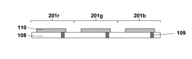
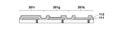
- the figure which shows the manufacturing method of the organic device of 1st Embodiment. The figure which shows the manufacturing method of the organic device of 1st Embodiment.
- the figure which shows the manufacturing method of the organic device of 1st Embodiment. which shows the manufacturing method of the organic device of 1st Embodiment.
- the figure which shows the manufacturing method of the organic device of 1st Embodiment The figure which shows the manufacturing method of the organic device of 1st Embodiment.
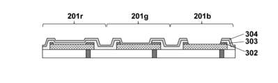
- the figure which shows the manufacturing method of the organic device of 1st Embodiment The schematic diagram which shows the cross-sectional structure of the organic device of 2nd Embodiment.
- the figure which shows the manufacturing method of the organic device of 2nd Embodiment The figure which shows the manufacturing method of the organic device of 2nd Embodiment.
- the figure which shows the manufacturing method of the organic device of 2nd Embodiment The figure which shows the manufacturing method of the organic device of 2nd Embodiment.
- the figure which shows the manufacturing method of the organic device of 2nd Embodiment The figure which shows the manufacturing method of the organic device of 2nd Embodiment.
- the figure which shows the manufacturing method of the organic device of 2nd Embodiment The figure which shows the manufacturing method of the organic device of 2nd Embodiment.
- the figure which shows the manufacturing method of the organic device of 2nd Embodiment The figure which shows the manufacturing method of the organic device of 2nd Embodiment.
- FIG. 1 schematically shows the cross-sectional structure of the organic device 1 of the first embodiment.
- FIG. 2 schematically shows the cross-sectional structure of the organic device 1 of the modified example of the first embodiment.
- the organic device 1 includes a first pixel 201r, a second pixel 201g, and a third pixel 201b.
- the first pixel 201r, the second pixel 201g, and the third pixel 201b are pixels having different structures of the optical adjustment film 114 described later.
- the first pixel 201r, the second pixel 201g, and the third pixel 201b are pixels in which the colors of light radiated from the organic device 1 to the outside are different from each other.
- the first pixel 201r emits red (R) light
- the second pixel 201g emits green (G) light
- the third pixel 201b emits blue (B) light.
- the organic device 1 may have a plurality of first pixels 201r, a plurality of second pixels 201g, and a plurality of third pixels 201b.
- the cross-sectional structure of FIGS. 1 and 2 is the cross section of the CC'line of FIG. Can correspond to.
- R, G, and B correspond to the first pixel 201r, the second pixel 201g, and the third pixel 201b, respectively.
- the organic device 1 may include a substrate such as a semiconductor substrate 101.
- a MOS transistor for driving a light emitting element (organic EL element) and an element separation region 102 (for example, STI) may be arranged on the semiconductor substrate 101.
- the MOS transistor may include a gate electrode 103 and a source / drain region 104.
- the first interlayer insulating film 105 may be arranged on the semiconductor substrate 101, and the first wiring layer 107 may be arranged on the first interlayer insulating film 105.
- the gate electrode 103 and the source / drain region 104 may be electrically connected to any of the first wiring patterns of the first wiring layer 107 via the first conductive plug 106.
- the first interlayer insulating film 105 may be, for example, a BPSG film formed by a thermal CVD method or a SiO 2 film formed by a plasma CVD method.
- the first wiring layer pattern of the first wiring layer 107 may be, for example, an AlCu film having a barrier metal such as Ti / TiN.
- the first conductive plug 106 can be, for example, a W plug having a barrier metal such as Ti / TiN.
- a second interlayer insulating film 108 may be arranged on the first wiring layer 107, and a plurality of reflecting portions (reflective films) 110 may be arranged on the second interlayer insulating film 108.
- the first wiring pattern of the first wiring layer 107 and the corresponding reflecting portion 110 can be electrically connected via the second conductive plug 109.
- the second interlayer insulating film 108 may be, for example, SiO 2 formed by a plasma CVD method.
- the plurality of reflecting portions 110 may be made of a reflective material.
- the material of the plurality of reflecting portions 110 is preferably a high reflectance material such as Al, Ag, Pt, and may be an alloy containing these.
- an alloy containing Al or Al as a main component is preferable because it is easy to achieve high definition.
- it may have a laminated structure, and may be an AlCu film having a barrier metal such as Ti / TiN between the second interlayer insulating film 108.
- the second conductive plug 109 can be, for example, a W film having a barrier metal such as Ti / TiN.
- the plurality of reflecting portions 110 may be arranged in the wiring layer.
- the optical adjusting film 114 may be arranged so as to cover the plurality of reflecting portions 110.
- the optical adjusting film 114 includes a first film 111, a second film 112 arranged (laminated) on the first film 111, and a third film 113 arranged (laminated) on the second film 112.
- the optical adjustment film 114 includes a portion composed of a laminated film of the first film 111, a second film 112, and a third film 113, and a portion composed of a laminated film of the second film 112 and the third film 113.
- a portion composed of a monolayer film composed of a third film 113 may be included.
- the optical adjusting film 114, or the first film 111, the second film 112, and the third film 113 are translucent insulating films, and may be composed of, for example, a SiO 2 film, a SiN film, or a SiON film.
- the second film 112 is arranged on the first film 111.
- the third film 113 is arranged on the second film 112, and the second film 112 is on the first film 111. Is located in.
- the first pixel 201r has an optical adjusting film 114r on the reflecting portion 110 for the first pixel 201r, and the optical adjusting film 114r is a first film 111, a second film 112, and a first film. It is composed of a laminated film of three films 113.
- the optical adjusting film 114r has a portion composed of a laminated film of the first film 111, the second film 112, and the third film 113 in the peripheral portion of the reflecting portion 110 for the first pixel 201r. Further, the optical adjusting film 114r has a portion composed of a laminated film of the first film 111, the second film 112, and the third film 113 in the central portion of the reflecting portion 110 for the first pixel 201r.
- the thickness of the optical adjusting film 114r in the central portion of the reflecting portion 110 for the first pixel 201r is Tr.
- the optical adjustment film 114r of the first pixel 201r has a step ⁇ Tr on its surface (upper surface).
- the step ⁇ Tr may be 0. That is, the step Tr is 0 or more.
- the step ⁇ Tr is 0 and is not shown. It is preferable that the film thickness of the optical adjustment film 114r located at the center of the reflection unit 110 and the film thickness of the optical adjustment film 114r located at the periphery of the reflection unit 110 are substantially the same.
- the central portion of a member is D from the center of gravity, where D is the distance from the center of gravity of the member to the end of the member in a plan view (plan view). It means within the range of / 3. Further, the peripheral portion of the member means the range of D / 8 from the end portion of the member toward the center of gravity of the member.
- the second pixel 201 g has an optical adjustment film 114 g.
- the optical adjusting film 114g has a portion composed of a laminated film of the first film 111, the second film 112, and the third film 113 in the peripheral portion of the reflecting portion 110 for the second pixel 201g. Further, the optical adjusting film 114g has a portion composed of a laminated film of the second film 112 and the third film 113 in the central portion of the reflecting portion 110 for the second pixel 201g.
- the thickness of the optical adjusting film 114g in the central portion of the reflecting portion 110 for the second pixel 201g is Tg.
- the optical adjustment film 114 g of the second pixel 201 g has a step ⁇ Tg on its surface (upper surface) due to the difference in thickness between the peripheral portion and the central portion.
- ⁇ Tg is greater than 0.
- the optical adjustment film 114g located at the center of the reflection unit 110 is preferably smaller than the film thickness of the optical adjustment film 114g located at the periphery of the reflection unit 110.
- the third pixel 201b has an optical adjustment film 114b.
- the optical adjusting film 114b has a portion composed of a laminated film of the first film 111, the second film 112, and the third film 113 in the peripheral portion of the reflecting portion 110 for the third pixel 201b. Further, the optical adjustment film 114b has a portion formed of a single-layer film made of the third film 113 in the central portion of the reflection portion 110 for the third pixel 201b.
- the thickness of the optical adjusting film 114b in the central portion of the reflecting portion 110 for the third pixel 201b is Tb.
- the optical adjustment film 114b of the third pixel 201b has a step ⁇ Tb on its surface (upper surface) due to the difference in thickness between the peripheral portion and the central portion.
- ⁇ Tb is greater than 0.
- the optical adjustment film 114b located in the central portion of the reflection portion 110 is preferably smaller than the film thickness of the optical adjustment film 114b located in the peripheral portion of the reflection portion 110.
- Tr> Tg and ⁇ Tr ⁇ Tg are satisfied.
- Such a configuration includes the magnitude of the leakage current between the first pixel 201r and the other pixels (second pixel 201g, third pixel 201b) and the second pixel 201g and the other pixel (first pixel 201r, first pixel 201b). This means that the difference from the magnitude of the leak current between the three pixels 201b) can be reduced.
- such a configuration is advantageous for keeping the leak current between the first pixel 201r and the other pixel and the leak current between the second pixel 201g and the other pixel within a constant value, and as a result. , It is advantageous to keep the leakage current between pixels within a constant value. Further, such a configuration is advantageous for making the leakage current between the lower electrode 115 and the upper electrode 120 equal for the first pixel 201r and the second pixel 201g, and suppresses deterioration of image quality due to color mixing. It is effective for.
- the thickness of the optical adjustment film 114r in the peripheral portion of the reflection portion 110 for the first pixel 201r and the thickness of at least a part of the optical adjustment film 114g in the peripheral portion of the reflection portion 110 for the second pixel 201g are omitted. It is preferable that they are the same.
- Tg> Tb and ⁇ Tg ⁇ Tb are satisfied.
- Such a configuration includes the magnitude of the leakage current between the second pixel 201g and the other pixels (first pixel 201r, third pixel 201b) and the third pixel 201b and the other pixel (first pixel 201r, third pixel 201b). This means that the difference from the magnitude of the leak current between the two pixels (201 g) can be reduced.
- such a configuration is advantageous for keeping the leakage current between the second pixel 201g and the other pixel and the leakage current between the third pixel 201b and the other pixel within a constant value, and as a result. , It is advantageous to keep the leakage current between pixels within a constant value. Further, such a configuration is advantageous for making the leakage current between the lower electrode 115 and the upper electrode 120 equal for the second pixel 201g and the third pixel 201b, and suppresses deterioration of image quality due to color mixing. It is effective for.
- the thickness of the optical adjustment film 114g in the peripheral portion of the reflection portion 110 for the second pixel 201g and the thickness of at least a part of the optical adjustment film 114b in the peripheral portion of the reflection portion 110 for the second pixel 201b are omitted. It is preferable that they are the same.
- Tr> Tg> Tb and ⁇ Tr ⁇ Tg ⁇ Tb are satisfied.
- Means to do Such a configuration means that the difference in the magnitude of the leakage current between the first pixel 201r, the second pixel 201g, and the third pixel 201b can be reduced. Therefore, such a configuration is advantageous for keeping the leakage current between pixels within a constant value.
- such a configuration is advantageous for making the leakage current between the lower electrode 115 and the upper electrode 120 equal in the first pixel 201r, the second pixel 201g, and the third pixel 201b, and the image quality due to color mixing is obtained. It is effective to suppress the decrease of.
- the thickness of at least a part of the optical adjustment film 114r, the optical adjustment film 114g, and the optical adjustment film 114b in the peripheral portion of the reflection portion 110 for each of the first pixel 201r, the second pixel 201g, and the third pixel 201b is It is preferable that they are substantially the same.
- a plurality of lower electrodes 115 may be arranged on the optical adjusting film 114 (114r, 114g, 114b).
- the plurality of lower electrodes 115 may be made of a transparent material, for example, indium tin oxide (ITO) or zinc oxide (IZO).
- ITO indium tin oxide
- IZO zinc oxide
- each lower electrode 115 extends to an opening 116 (contact hole) provided in the optical adjustment film 114, and each lower electrode 115 is a reflection arranged below the opening 116 (contact hole). It is electrically connected to the peripheral portion of the portion 110 at the opening 116.
- ITO indium tin oxide
- IZO zinc oxide
- each lower electrode 115 is electrically connected to the peripheral portion of the reflection portion 110 arranged below the lower electrode 115 by a plug 117 penetrating the optical adjustment film 114.
- the plug 117 can be, for example, a W plug having a barrier metal such as Ti / TiN.
- the organic device 1 may further include an insulating film 118 covering each peripheral portion of the plurality of lower electrodes 115 and an optical adjusting film 114 between the plurality of lower electrodes 115.
- the lower electrode 115 may have a central portion and a peripheral portion surrounding the central portion, and the central portion and the peripheral portion may have different thicknesses, and the central portion may be smaller in thickness than the peripheral portion.
- the peripheral portion may be a region of the lower electrode 115 covered with the insulating film 118.
- the lower electrode 115 may have a step along the optical adjustment layer 114.
- the step of the optical adjustment layer 114 may have a portion that is inclined with respect to the substrate.
- the insulating film 118 may be, for example, a SiO 2 film formed by a plasma CVD method.
- the insulating film 118 is arranged so as to electrically insulate the plurality of lower electrodes 115 from each other.
- An organic functional film 119 can be arranged on the insulating film 118.
- the organic functional film 119 includes at least an organic light emitting material layer, and may also include, for example, a charge transport layer, a charge block layer, and the like.
- the organic functional film 119 may be continuously arranged on the first pixel 201r and the second pixel 202g. "Continuously arranged" means that one organic functional film in which the organic functional films are connected and arranged across the organic functional films is shared by the first pixel and the second pixel. it can.
- the organic functional film 119 may be continuously arranged on the third pixel 203b in addition to the first pixel and the second pixel.
- the upper electrode 120 may be arranged on the organic functional film 119.
- the upper electrode 120 may be made of a transparent material so as to transmit the light generated by the organic functional film 119 without blocking it.
- the upper electrode 120 may be composed of, for example, a thin film of gold, platinum, silver, aluminum, chromium, magnesium or an alloy thereof.
- a sealing film 121 may be placed on the upper electrode 120.
- the sealing film 121 is a film for preventing moisture from entering the semiconductor substrate 101, the organic functional film 119, and the upper electrode 120, and may be composed of, for example, a SiN film formed by a plasma CVD method.
- a color filter layer 122 may be arranged on the sealing film 121.
- the color filter layer 122 may include a color filter 122r for the first pixel 201r, a color filter 122g for the second pixel 201g, and a color filter 123b for the third pixel 201b. Further, a microlens may be provided on the upper side or the lower side of the color filter layer 122 (not shown). The microlens may be used for the purpose of improving luminous efficiency.
- An electric signal is sent from the MOS transistor formed on the semiconductor substrate 101 to each lower electrode 115, and the organic functional film 119 generates light.
- the light emitted from the organic functional film 119 toward the semiconductor substrate 101 is reflected by the reflecting unit 110.
- the light emitted from the organic functional film 119 toward the upper electrode 120 and the light reflected by the reflecting portion 110 are the optical adjusting film 114 in the central portion of the reflecting portion 110 for the pixels 201r, 201g, and 201b, respectively. It resonates and is amplified at a wavelength corresponding to the thickness Tr, Tg, and Tb.
- the light amplified in this way is emitted through the color filters 122r, 122g and 122b.
- the thickness Tr, Tg, and Tb of the optical adjustment film 114 in the central portion of the reflecting portion 110 for each of the pixels 201r, 201g, and 201b are determined in consideration of the light amplification effect.
- the steps ⁇ Tr, ⁇ Tg, and ⁇ Tb can be determined so that the leakage current between the pixels is kept within a constant value.
- the steps ⁇ Tr, ⁇ Tg, and ⁇ Tb can be determined so that, for example, the thickness of the optical adjusting film 114 at the peripheral portion of the reflecting portion 110 for each of the pixels 201r, 201g, and 201b is equal to each other.
- Tr, Tg, and Tb can be read as T1, T2, and T3, and ⁇ Tr, ⁇ Tg, and ⁇ Tb can be read as ⁇ T1, ⁇ T2, and ⁇ T3, and T1>T2> T3 and ⁇ T1 ⁇ T2 ⁇ T3 can be satisfied.
- Tr and Tg can be read as T1 and T2
- ⁇ Tr and ⁇ Tg can be read as ⁇ T1 and ⁇ T2 and it is desirable that T1> T2 and ⁇ T1 ⁇ T2 are satisfied.
- Tg and Tb can be read as T1 and T2
- ⁇ Tg and ⁇ Tb can be read as ⁇ T1 and ⁇ T2
- the thickness Tr, Tg, and Tb of the optical adjustment film 114 in the central portion of the reflecting portion 110 for each of the red light emitting pixel, the green light emitting pixel, and the blue light emitting pixel are Tr>Tg> Tb.
- the case where the steps ⁇ Tr, ⁇ Tg, and ⁇ Tb are ⁇ Tr ⁇ Tg ⁇ Tb has been described, but the relationship of magnitude depending on the emission color is not limited to the above relationship.
- Relationship A Tr>Tb> Tg, ⁇ Tr ⁇ Tb ⁇ Tg Relationship B: Tg>Tr> Tb, ⁇ Tg ⁇ Tr ⁇ Tb Relationship C: Tg>Tb> Tr, ⁇ Tg ⁇ Tb ⁇ Tr Relationship D: Tb>Tr> Tg, ⁇ Tb ⁇ Tr ⁇ Tg Relationship E: Tb>Tg> Tr, ⁇ Tb ⁇ Tg ⁇ Tr
- an AlCu film (for example, 0.5 (atm%) of Cu was added by a sputtering method) was added onto the second interlayer insulating film 108 on which the conductive plug 109 was formed. A film) is formed. After that, the AlCu film can be patterned by a photolithography step and a dry etching step to form a plurality of reflecting portions 110.
- a first film 111a made of a SiO 2 film by a plasma CVD method is formed. Then, in the step shown in FIG.
- the portion of the first film 111a located above the central portion of the reflecting portion 110 of the second pixel 201 g is removed by the photolithography step and the dry etching step, and the first The film 111b is formed.
- a second film 112a made of a SiO 2 film by a plasma CVD method is formed.
- the portion of the first film 11b and the second film 112a located above the central portion of the reflecting portion 110 of the third pixel 201b is opened by the photolithography step and the dry etching step. Will be done. As a result, the first film 111 and the second film 112 are formed.
- a third film 113 made of a SiO 2 film by a plasma CVD method is formed, whereby the first film 111, the second film 112, and the third film 113 are formed.
- the optical adjusting film 114 is formed.
- the optical adjustment film 114 includes a first optical adjustment film 114r for the first pixel 201r, a second optical adjustment film 114g for the second pixel 201g, and a third optical adjustment film 114b for the third pixel 201b. ..
- the first optical adjustment film 114r has a thickness Tr and a step ⁇ Tr
- the second optical adjustment film 114g has a thickness Tg and a step ⁇ Tg
- the third optical adjustment film 114b has a thickness Tb and a step ⁇ Tb.
- the thicknesses of the optical adjusting films 114r, 114g, 114b at the center of the reflecting portion 110 for each of the first pixel 201r, the second pixel 201g, and the third pixel 201b. Can be easily controlled with high accuracy.
- the thickness of the optical adjustment film 114 can be controlled with high accuracy, it is possible to control optical characteristics such as luminous efficiency and chromaticity of the light emitting pixel with high accuracy.
- the thicknesses of the optical adjustment films 114r, 114g, and 114b in the central portion of the reflecting portion 110 for each of the first pixel 201r, the second pixel 201g, and the third pixel 201b are controlled by the etching time. There is also a way to do it. However, it is difficult to control their thickness with high accuracy by such a method of controlling by etching time.
- an opening 116 is formed in the optical adjustment film 114 by a photolithography process and a dry etching process.
- an electrode film such as an ITO film or an IZO film is formed by a sputtering method, and the electrode film is patterned by a photolithography step and a dry etching step to form a plurality of lower electrodes 115.
- the edge of the photoresist pattern for forming the opening 116 and the lower electrode 115 can be arranged in a region (peripheral portion of the pixel) where the height difference between the pixels 201r, 201g, and 201b is small.
- the processing error of the opening 116 and the lower electrode 115 between the pixels 201r, 201g, and 201b it is preferable that at least a part of the end portion of the lower electrode 115 is arranged so as to overlap the peripheral portion of the reflection portion 110 of each pixel in a plan view.
- SiO 2 by a plasma CVD method is used so as to cover the peripheral portion of each of the plurality of lower electrodes 115 and the optical adjustment film 114 between the plurality of lower electrodes 115.
- a film is formed.
- the SiO 2 film is patterned in a photolithography step and a dry etching step to form an insulating film 118.
- the processing error between the pixels 201r, 201g, and 201b can be reduced.
- the organic functional film 119 and the upper electrode 120 are formed in this order by a vacuum vapor deposition method using a thin-film deposition mask, and then, for example, a sealing film 121 is formed by a CVD method.
- the color filter layer 122 can be formed by the photolithography method.
- the microlens may be formed on the upper side or the lower side of the color filter layer in order to improve the luminous efficiency.
- FIG. 4 schematically shows the cross-sectional structure of the organic device 1 of the second embodiment. Matters not mentioned as the second embodiment may follow the first embodiment.
- a plurality of reflecting portions 301 are arranged on the second interlayer insulating film 108 instead of the plurality of reflecting portions 110 in the first embodiment.
- An antireflection electrode 302 is arranged on each reflection portion 301 so as to come into contact with the reflection portion 301.
- Each reflecting portion 301 and the antireflection electrode 302 are electrically connected to each other.
- Each reflecting portion 301 may be composed of, for example, an AlCu film having a barrier metal such as Ti / TiN.
- the antireflection electrode 302 may be composed of, for example, a layer containing at least one of TiN, Ti, W, Co, Ta, and TaN, and may be a laminated structure thereof.
- the film thickness of the antireflection electrode 302 is preferably about 1 to 200 nm.
- the antireflection electrode can be formed by a known technique such as a sputtering method or a thin film deposition method.
- the optical adjustment film 306 may be arranged so as to cover the plurality of reflective portions 301 and the plurality of antireflection electrodes 302.
- the optical adjusting film 306 includes a portion composed of a laminated film of the first film 303, a second film 304, and a third film 305, a portion composed of a laminated film of the second film 304 and the third film 305, and a first film. It may include a portion composed of a monolayer film composed of three films 305.
- the optical adjusting film 306, or the first film 303, the second film 304, and the third film 305 may be composed of, for example, a SiO 2 film.
- Optical adjustment films 306r having different film thicknesses by providing openings in a part of the interlayer insulating film material and the antireflection electrode material on the reflective portion 301 of the first pixel 201r, the second pixel 201g, and the third pixel 201b. , 306g, 306b are formed.
- the respective film thicknesses are Tr, Tg, and Tb and the step film thickness formed by the opening is ⁇ Tr, ⁇ Tg, and ⁇ Tb
- the relationship between the film thickness and the step film thickness is Tr>Tg> Tb, ⁇ Tr ⁇ Tg. ⁇ Tr.
- the member constituting the antireflection electrode 302 is at least a part of the peripheral portion of the reflection portion 301, and particularly preferably formed so as to surround the reflection portion 301.
- the thickness of the reflective portion may be different between the central portion and the peripheral portion, and the thickness of the central portion may be smaller than that of the peripheral portion.
- the lower electrode 307 is arranged on the optical adjustment film 306.
- the lower electrode 307 is preferably a transparent material and is formed using indium tin oxide (ITO) or indium zinc oxide (IZO).
- the optical adjusting film 306 is provided with an opening 308, and the antireflection electrode 302 and the lower electrode 307 are electrically connected at the opening 308.
- the reflective portion 301 is made of AlCu and the lower electrode 307 is made of a material containing oxygen
- aluminum oxide is formed, which is conductive. Can lead to defects.
- the insulating film 118, the organic functional film 119, the upper electrode 120, the sealing film 121, and the color filter 122 may be formed on the lower electrode 307.
- the first pixel 201r has an optical adjusting film 306r on the reflecting portion 301, and the optical adjusting film 306r is a laminated film of the first film 303, the second film 304, and the third film 305. It is configured.
- the optical adjusting film 306r has a portion composed of a laminated film of the first film 303, the second film 304, and the third film 305 in the peripheral portion of the reflecting portion 301 for the first pixel 201r. Further, the optical adjusting film 306r has a portion composed of a laminated film of the first film 303, the second film 304, and the third film 305 in the central portion of the reflecting portion 301 for the first pixel 201r.
- the thickness of the optical adjustment film 306r in the central portion of the reflection portion 301 for the first pixel 201r is Tr.
- the optical adjustment film 306r of the first pixel 201r has a step ⁇ Tr on its surface (upper surface).
- the step ⁇ Tr is larger than 0.
- it is preferable that the step on the upper surface of the central portion of the reflective portion 301 of the first pixel 201r and the upper surface of the antireflection electrode 302 are substantially the same as the step ⁇ Tr.
- the second pixel 201 g has an optical adjustment film 306 g.
- the optical adjusting film 306g has a portion composed of a laminated film of the first film 303, the second film 304, and the third film 305 in the peripheral portion of the reflecting portion 301 for the second pixel 201g. Further, the optical adjusting film 306g has a portion composed of a laminated film of the second film 112 and the third film 113 in the central portion of the reflecting portion 301 for the second pixel 201g.
- the thickness of the optical adjusting film 306g in the central portion of the reflecting portion 301 for the second pixel 201g is Tg.
- the optical adjustment film 306 g of the second pixel 201 g has a step ⁇ Tg on its surface (upper surface) due to the difference in thickness between the peripheral portion and the central portion and the thickness of the antireflection electrode.
- ⁇ Tg is greater than 0.
- the third pixel 201b has an optical adjustment film 306b.
- the optical adjusting film 306b has a portion composed of a laminated film of the first film 303, the second film 304, and the third film 305 in the peripheral portion of the reflecting portion 301 for the third pixel 201b. Further, the optical adjustment film 306b has a portion formed of a single-layer film composed of the third film 305 in the central portion of the reflection portion 301 for the third pixel 201b.
- the thickness of the optical adjustment film 306b in the central portion of the reflection portion 301 for the third pixel 201b is Tb.
- the optical adjustment film 306b of the third pixel 201b has a step ⁇ Tb on its surface (upper surface) due to the difference in thickness between the peripheral portion and the central portion and the thickness of the antireflection electrode.
- ⁇ Tb is greater than 0.
- Tr> Tg and ⁇ Tr ⁇ Tg are satisfied. This reduces the difference between the thickness of the optical adjustment film 306r in the peripheral portion of the reflection portion 301 for the first pixel 201r and the thickness of the optical adjustment film 306g in the peripheral portion of the reflection portion 301 for the second pixel 201g. Means that.
- Such a configuration includes the magnitude of the leakage current between the first pixel 201r and the other pixels (second pixel 201g, third pixel 201b) and the second pixel 201g and the other pixel (first pixel 201r, first pixel 201b). This means that the difference from the magnitude of the leak current between the three pixels 201b) can be reduced.
- such a configuration is advantageous for keeping the leak current between the first pixel 201r and the other pixel and the leak current between the second pixel 201g and the other pixel within a constant value, and as a result. , It is advantageous to keep the leakage current between pixels within a constant value. Further, such a configuration is advantageous for making the leakage current between the lower electrode 307 and the upper electrode 120 equal for the first pixel 201r and the second pixel 201g, and suppresses deterioration of image quality due to color mixing. It is effective for.
- the thickness of the optical adjustment film 306r in the peripheral portion of the reflection portion 301 for the first pixel 201r and the thickness of at least a part of the optical adjustment film 306g in the peripheral portion of the reflection portion 301 for the second pixel 201g is preferable that they are substantially the same.
- Tg> Tb and ⁇ Tg ⁇ Tb are satisfied.
- Such a configuration includes the magnitude of the leakage current between the second pixel 201g and the other pixels (first pixel 201r, third pixel 201b) and the third pixel 201b and the other pixel (first pixel 201r, third pixel 201b). This means that the difference from the magnitude of the leak current between the two pixels (201 g) can be reduced.
- such a configuration is advantageous for keeping the leakage current between the second pixel 201g and the other pixel and the leakage current between the third pixel 201b and the other pixel within a constant value, and as a result. , It is advantageous to keep the leakage current between pixels within a constant value. Further, such a configuration is advantageous for making the leakage current between the lower electrode 307 and the upper electrode 120 equal for the second pixel 201g and the third pixel 201b, and suppresses deterioration of image quality due to color mixing. It is effective for.
- the thickness of the optical adjustment film 306g in the peripheral portion of the reflection portion 301 for the first pixel 201g and the thickness of at least a part of the optical adjustment film 306b in the peripheral portion of the reflection portion 301 for the second pixel 201b it is preferable that they are substantially the same.
- Tr> Tg> Tb and ⁇ Tr ⁇ Tg ⁇ Tb are satisfied.
- Means to do Such a configuration means that the difference in the magnitude of the leakage current between the first pixel 201r, the second pixel 201g, and the third pixel 201b can be reduced. Therefore, such a configuration is advantageous for keeping the leakage current between pixels within a constant value.
- such a configuration is advantageous for making the leakage current between the lower electrode 307 and the upper electrode 120 equal in the first pixel 201r, the second pixel 201g, and the third pixel 201b, and the image quality due to color mixing is obtained. It is effective to suppress the decrease of.
- the thickness of at least a part of the optical adjustment film 306r, the optical adjustment film 306g, and the optical adjustment film 306b in the peripheral portion of the reflection portion 301 for each of the first pixel 201r, the second pixel 201g, and the third pixel 201b is It is preferable that they are substantially the same.
- the thickness Tr, Tg, and Tb of the optical adjustment film 306 in the central portion of the reflection portion 301 for each of the red light emitting pixel, the green light emitting pixel, and the blue light emitting pixel are Tr>Tg> Tb.
- the case where the steps ⁇ Tr, ⁇ Tg, and ⁇ Tb are ⁇ Tr ⁇ Tg ⁇ Tb has been described, but the relationship of magnitude depending on the emission color is not limited to the above relationship. For example, there may be the following relationships.
- an AlCu film (for example, 0.5 (atm%) of Cu) was added onto the second interlayer insulating film 108 on which the conductive plug 109 was formed, for example, by a sputtering method.
- An Al film) and a TiN film (antireflection film) are formed.
- the AlCu film and the laminated film of the TiN film are patterned by a photolithography step and a dry etching step, and a plurality of laminated bodies composed of the laminated film of the reflection portion 301 and the antireflection electrode 302a are formed.
- the reflection wave from the AlCu film is suppressed by the antireflection electrode 302a, so that the fine reflection portion 301 can be formed.
- the plurality of antireflection electrodes 302b are removed by removing the antireflection electrode 302a at the center of the reflection portion 301 of each first pixel 201r by a photolithography step and a dry etching step. It is formed.
- a first film 303a made of a SiO 2 film by a plasma CVD method is formed.
- the portion of the first film 303a and the antireflection electrode 302a located above the central portion of the reflection portion 301 of the second pixel 201g is removed by a photolithography step and a dry etching step. Will be done.
- the antireflection electrode 302c and the first film 303b are formed.
- a second film 304a made of a SiO 2 film by a plasma CVD method is formed.
- the portion of the antireflection electrode 302, the first film 303b, and the second film 304a located above the central portion of the reflection portion 301 of the third pixel 201b is the photolithography step. It is removed by a dry etching process. As a result, the antireflection electrode 302, the first film 303, and the second film 304 are formed.
- a third film 305 made of a SiO 2 film by a plasma CVD method is formed, whereby the first film 303, the second film 304, and the third film 305 are formed.
- the optical adjusting film 306 is formed.
- the optical adjustment film 306 includes a first optical adjustment film 306r for the first pixel 201r, a second optical adjustment film 306g for the second pixel 201g, and a third optical adjustment film 306b for the third pixel 201b. ..
- the first optical adjustment film 306r has a thickness Tr and a step ⁇ Tr
- the second optical adjustment film 306g has a thickness Tg and a step ⁇ Tg
- the third optical adjustment film 306b has a thickness Tb and a step ⁇ Tb.
- the thicknesses of the optical adjusting films 306r, 306g, 306b at the center of the reflecting portion 110 for each of the first pixel 201r, the second pixel 201g, and the third pixel 201b. Can be easily controlled with high accuracy.
- the thickness of the optical adjustment film 114 can be controlled with high accuracy, it is possible to control optical characteristics such as luminous efficiency and chromaticity of the light emitting pixel with high accuracy.
- the thicknesses of the optical adjusting films 306r, 306g, and 306b in the central portion of the reflecting portion 110 for each of the first pixel 201r, the second pixel 201g, and the third pixel 201b are controlled by the etching time. There is also a way to do it. However, it is difficult to control their thickness with high accuracy by such a method of controlling by etching time.
- an opening 308 (contact hole) is formed in the optical adjustment film 114 by a photolithography step and a dry etching step.
- an electrode film such as an ITO film or an IZO film is formed by a sputtering method, and the electrode film is patterned by a photolithography step and a dry etching step to form a plurality of lower electrodes 307.
- the edge of the photoresist pattern for forming the opening 308 and the lower electrode 307 can be arranged in a region (peripheral portion of the pixel) where the height difference between the pixels 201r, 201g, and 201b is small.
- the processing error of the opening 308 and the lower electrode 307 between the pixels 201r, 201g, and 201b it is preferable that at least a part of the end portion of the lower electrode 307 is arranged so as to overlap with the antireflection electrode 302 in the peripheral portion of the reflection portion 110 of each pixel in a plan view.
- SiO 2 by a plasma CVD method is used so as to cover the peripheral portion of each of the plurality of lower electrodes 307 and the optical adjustment film 306 between the plurality of lower electrodes 307.
- a film is formed.
- the SiO 2 film is patterned in a photolithography step and a dry etching step to form an insulating film 118.
- the processing error between the pixels 201r, 201g, and 201b can be reduced.
- the organic functional film 119 and the upper electrode 120 are sequentially formed by a vacuum vapor deposition method using, for example, a thin-film deposition mask.
- the sealing film 121 can be formed by the CVD method, and then the color filter layer 122 can be formed by the photolithography method.
- the microlens may be formed above or below the color filter layer.
- FIG. 6 schematically shows a plan view of the organic device of the third embodiment.
- FIG. 7A schematically shows the cross-sectional structure of the line AA'of FIG.
- FIG. 7B schematically shows the cross-sectional structure of the line BB'of FIG. Matters not mentioned as the third embodiment may follow the first or second embodiment.
- the third wiring layer including the reflective film 402 and the wiring pattern 401 is arranged on the second interlayer insulating film 108.
- the first pixel 201r, the second pixel 201b, and the third pixel 201b include a lower electrode 403.
- Each lower electrode 403 may have, for example, a hexagonal shape, but may have another polygonal shape, or may have a shape other than a polygonal shape.
- the third wiring layer in which the reflective film 402 and the wiring pattern 401 are arranged is a wiring layer for electrically connecting the lower electrode 403 and the wiring layer below it (not shown).
- the reflective film 402 and the wiring pattern 401 are electrically insulated from each other.
- the reflective film 402 is a conductor commonly provided for a plurality of pixels including the first pixel 201r, the second pixel 201b, and the third pixel 201b.
- the reflective film 402 is not divided between pixels and extends over a plurality of pixels in the pixel array region of the organic device. Even in such a configuration, the reflective film 402 can be considered to include a plurality of reflective portions corresponding to the plurality of lower electrodes 403.
- the central portion of the reflective portion for each pixel is a portion that overlaps with the central portion of the lower electrode 403 arranged on the central portion, and the peripheral portion of the reflective portion for each pixel is arranged on the central portion. It can be considered that it overlaps with the peripheral portion of the lower electrode 403.
- An optical adjustment film 404 according to the first or second embodiment is arranged on the reflection film 402 and the wiring pattern 401.
- a lower electrode 403 may be placed on the optical adjustment film 404.
- the lower electrode 403 and the wiring pattern 401 of the third wiring layer can be electrically connected at the opening 405 provided in the optical adjustment film 404.
- the potential of the reflective film 402 can be arbitrarily set.
- the potential of the reflective film 402 is preferably set so that the potential difference between the upper electrode and the reflective film 402 is lower than the light emission threshold voltage (threshold voltage at which the organic functional film operates) of the organic light emitting element. Due to manufacturing variations, when the reflective film 402 and the wiring pattern 401 of a certain pixel are electrically connected, the potential of the wiring pattern 401 becomes the same as the potential of the reflective film 402.
- the wiring pattern 401 and the lower electrode 403 have the same potential, when the potential difference between the reflective film 402 and the upper electrode is set to be equal to or lower than the emission threshold voltage of the organic light emitting element, the reflective film 402 and the lower electrode 403 are electrically connected. Since the physically connected pixels do not emit light, it does not cause a large pixel defect.
- FIG. 8 shows the planar arrangement of the third wiring layer of the fourth embodiment.
- FIG. 9A schematically shows the cross-sectional structure of the DD'line of FIG.
- FIG. 9B schematically shows the cross-sectional structure of the line EE'of FIG. Matters not mentioned as the fourth embodiment may follow the first to third embodiments.
- the third wiring layer including the reflective film 504 and the wiring pattern 503 is arranged on the second interlayer insulating film 108.
- the first pixel 201r, the second pixel 201b, and the third pixel 201b include a lower electrode 509.
- Each lower electrode 509 may have, for example, a hexagonal shape, but may have another polygonal shape, or may have a shape other than a polygonal shape.
- the pixel arrangement can be any arrangement such as a stripe arrangement, a delta arrangement, a Bayer arrangement, and a pentile arrangement.
- the delta arrangement is suitable because it is easy to arrange circular microlenses.
- the third wiring layer in which the reflective film 504 and the wiring pattern 503 are arranged is a wiring layer for electrically connecting the lower electrode 509 and the wiring layer below it.
- the reflective film 504 and the wiring pattern 503 are electrically insulated by removing the conductive material 502 on the reflective material 501 in the third wiring layer.
- the wiring pattern 503 has a configuration in which the conductive material 502 is laminated on the reflective material 501.
- the reflective material 501 may have reflectivity and conductivity, and for example, a high reflectance material such as Al, Ag, or Pt is preferable. Further, an alloy containing these may be used, or a laminated structure may be used. In particular, an alloy containing Al is preferable.
- the conductive material 502 may have conductivity, and is particularly preferably a material that is stable in contact with the reflective material 501 and the lower electrode 509. Further, the conductive material 502 preferably has a low reflectance, and particularly preferably contains TiN and Ti. The film thickness of the conductive material 502 is preferably about 1 to 100 nm.
- the reflective film 504 is a conductor commonly provided for a plurality of pixels including the first pixel 201r, the second pixel 201b, and the third pixel 201b, and the reflective material 501 and It is composed of a conductive material 502.
- the reflective film 504 is not divided between pixels and extends over a plurality of pixels in the pixel array region of the organic device. Even in such a configuration, the reflective film 504 can be considered to include a plurality of reflective portions corresponding to the plurality of lower electrodes 403.
- the central portion of the reflective portion for each pixel is a portion that overlaps the central portion of the lower electrode 403 arranged on the central portion in a plan view, and the peripheral portion of the reflective portion for each pixel is above it. It can be considered that it overlaps with the peripheral portion of the arranged lower electrode 403 in a plan view.
- the conductive material 502 is removed from the reflective portion, and the reflective material 501 is exposed.
- the conductive material 502 is provided in at least a part of the peripheral portion of the reflective portion. In particular, it is preferable that the conductive material 502 is provided so as to surround the central portion of the reflective portion in the peripheral portion of the reflective portion.
- the conductive material 502 is also provided between the pixels of the first pixel 201r, the second pixel 201b, and the third pixel 201b.
- the conductive material 502 provided around the reflective portion as a material having a lower reflectance than that of the reflective material 501, it is possible to reduce stray light and improve the contrast.
- the optical adjusting film 508 according to the optical adjusting film of the first to third embodiments is arranged.
- a plurality of lower electrodes 509 may be arranged on the optical adjusting film 508.
- the organic device 1 may further include an insulating film 510 covering each peripheral portion of the plurality of lower electrodes 509 and an optical adjusting film 508 between the plurality of lower electrodes 509.
- the insulating film 510 corresponds to the insulating film 118 in the first embodiment.
- the lower electrode 509 and the wiring pattern 503 of the third wiring layer can be electrically connected at the opening 511 provided in the optical adjustment film 508. Since the reflective film 504 arranged on the third wiring layer and the plurality of wiring patterns 503 are electrically insulated, the plurality of lower electrodes 509 corresponding to the plurality of wiring patterns can be electrically connected.
- the potential of the reflective film 504 can be arbitrarily set. In particular, it is preferable that the potential difference between the reflective film 504 and the upper electrode is set to be equal to or lower than the emission threshold voltage of the organic light emitting element. Due to manufacturing variations, when the reflective film 504 and the wiring pattern 503 of a certain pixel are electrically connected, the potential of the wiring pattern 503 becomes the same as the potential of the reflective film 504. When the potential difference between the reflective film 504 and the upper electrode is set to be equal to or lower than the emission threshold voltage of the organic light emitting element, the pixels electrically connected to the reflective film 504 do not emit light, so that a large pixel defect does not occur.
- FIG. 10 schematically shows a cross-sectional view of the organic device of the fifth embodiment. Matters not mentioned as the fifth embodiment may follow the first to fourth embodiments.
- a gap 520 is provided between the reflective film 504 and the wiring pattern 503.
- the insulating property between the reflective film 504 formed in the same layer and the wiring pattern 503 can be improved.
- the gap 520 is preferably provided so as to surround the outer circumference of the wiring pattern.
- the void 520 is preferably filled with a vacuum or an inert gas. Further, when the reflective film is electrically separated for each pixel, it is preferable that a gap 520 is provided between the reflective films for each pixel. Further, the void 520 can be formed by any method. For example, the gap 520 can be formed by etching the optical adjustment film 508 in a groove shape. As another method, the gap 502 is formed by forming the reflective film 504 or the wiring pattern 503 of the third wiring layer by etching and forming the optical adjustment film 508 by a relatively isotropic growth film forming method. It is possible to do. The upper portion of the void 502 is preferably covered with an insulating film, and more preferably covered with an optical adjusting film 508.
- the organic EL element (organic light emitting element) has a structure in which an anode, an organic compound layer (organic functional film), and a cathode are arranged on a substrate.
- a protective layer, a color filter, or the like may be provided on the cathode.
- a flattening layer may be provided between the color filter and the protective layer.
- the flattening layer can be made of acrylic resin or the like.
- the substrate examples include quartz, glass, silicon wafer, resin, metal and the like.
- a switching element such as a transistor or wiring may be provided on the substrate, and an insulating layer may be provided on the switching element or wiring.
- the material of the insulating layer does not matter as long as it is possible to form a contact hole in order to ensure the continuity between the anode 2 and the wiring and to secure insulation from the wiring that is not connected.
- a resin such as polyimide, silicon oxide, silicon nitride, or the like can be used.
- a pair of electrodes can be used as the electrodes.
- the pair of electrodes may be an anode and a cathode.
- the electrode having a high potential is the anode and the other is the cathode.
- the electrode that supplies holes to the light emitting layer is the anode, and the electrode that supplies electrons is the cathode.
- the lower electrode may be an anode and the upper electrode may be a cathode, or the lower electrode may be a cathode and the upper electrode may be an anode.
- the lower electrode and the upper electrode may be translucent, and may be reflective or absorbent.
- a material having a work function as large as possible is preferable.
- elemental metals such as gold, platinum, silver, copper, nickel, palladium, cobalt, selenium, vanadium, tungsten, etc., mixtures containing these, or alloys containing these can be used.
- metal oxides such as tin oxide, zinc oxide, indium oxide, indium tin oxide (ITO), and indium zinc oxide can be used.
- conductive polymers such as polyaniline, polypyrrole and polythiophene can also be used.
- the anode may be composed of one layer or may be composed of a plurality of layers.
- the electrode When the electrode is used as a reflective film, for example, chromium, aluminum, silver, titanium, tungsten, molybdenum, alloys thereof, laminated ones, etc. can be used.
- an oxide transparent conductive layer such as indium tin oxide (ITO) or zinc oxide can be used, but the present invention is not limited thereto.
- Photolithography technology can be used to form the electrodes.
- a material having a small work function is preferable as a constituent material of the cathode.
- a material having a small work function examples thereof include alkali metals such as lithium, alkaline earth metals such as calcium, simple metals such as aluminum, titanium, manganese, silver, lead and chromium, or mixtures containing these.
- an alloy in which these metal simple substances are combined can also be used.
- magnesium-silver, aluminum-lithium, aluminum-magnesium, silver-copper, zinc-silver and the like can be used.
- a metal oxide such as indium tin oxide (ITO).
- ITO indium tin oxide
- the cathode may have a single-layer structure or a multi-layer structure.
- silver is preferably used, and more preferably a silver alloy is used in order to suppress the aggregation of silver.
- the ratio of the alloy does not matter. For example, it may be 1: 1.
- the method for forming the cathode is not particularly limited, but a vapor deposition heating method, a direct current or alternating current sputtering method, or the like can be used. The DC and AC sputtering methods are more preferable because they have good film coverage and can easily reduce the resistance.
- a protective layer may be provided on the upper electrode.
- a passivation film such as silicon nitride may be provided on the cathode to suppress the infiltration of water or the like into the organic EL layer.
- a protective layer using an atomic layer deposition method may be provided after the film formation by the CVD method.
- a color filter may be provided on the protective layer.
- a color filter considering the size of the organic light emitting element may be provided on another substrate and bonded to the substrate provided with the organic light emitting element, or a photolithography technique may be used on the protective layer shown above.
- the color filter may be patterned.
- the color filter may be made of a polymer. Further, the microlens may be formed above or below the color filter layer.
- a flattening layer may be provided between the color filter and the protective layer.
- the flattening layer may be composed of an organic compound and may be a small molecule or a polymer, but a polymer is preferable.
- the flattening layers may be provided above and below the color filter, and the constituent materials thereof may be the same or different. Specific examples thereof include polyvinylcarbazole resin, polycarbonate resin, polyester resin, ABS resin, acrylic resin, polyimide resin, phenol resin, epoxy resin, silicon resin, urea resin and the like.
- a facing substrate may be provided on the flattening layer.
- the facing substrate is called a facing substrate because it is provided at a position corresponding to the above-mentioned substrate.
- the constituent material of the facing substrate may be the same as that of the above-mentioned substrate.
- the organic compound layer (hole injection layer, hole transport layer, electron blocking layer, light emitting layer, hole blocking layer, electron transport layer, electron injection layer, etc.) constituting the organic light emitting device according to the embodiment of the present invention is , Is formed by the method shown below.
- a dry process such as vacuum vapor deposition, ionization vapor deposition, sputtering, or plasma can be used.
- a wet process in which a layer is formed by dissolving in an appropriate solvent and forming a layer by a known coating method (for example, spin coating, dipping, casting method, LB method, inkjet method, etc.) can also be used.
- the film can be formed by combining with an appropriate binder resin.
- binder resin examples include polyvinylcarbazole resin, polycarbonate resin, polyester resin, ABS resin, acrylic resin, polyimide resin, phenol resin, epoxy resin, silicon resin, urea resin and the like.
- the above is an example, and the binder resin is not limited to these.
- binder resins may be used alone as a homopolymer or a copolymer, or may be used as a mixture of two or more kinds. Further, if necessary, known additives such as plasticizers, antioxidants, and ultraviolet absorbers may be used in combination.
- the organic device can be used as a component of a display device or a lighting device.
- applications such as an exposure light source of an electrophotographic image forming apparatus, a backlight of a liquid crystal display device, and a light emitting device having a color filter as a white light source.
- the display device has an image input unit for inputting image information from an area CCD, a linear CCD, a memory card, etc., has an information processing unit for processing the input information, and displays the input image on the display unit.
- An image information processing device may be used.
- the display unit of the image pickup device or the inkjet printer may have a touch panel function.
- the drive method of this touch panel function may be an infrared method, a capacitance method, a resistance film method, or an electromagnetic induction method, and is not particularly limited.
- the display device may be used as a display unit of a multifunction printer.
- FIG. 11 is a schematic view showing an example of the display device according to the present embodiment.
- the display device 1000 may have a touch panel 1003, a display panel 1005, a frame 1006, a circuit board 1007, and a battery 1008 between the upper cover 1001 and the lower cover 1009.
- Flexible print circuits FPC1002 and 1004 are connected to the touch panel 1003 and the display panel 1005.
- a transistor is printed on the circuit board 1007.
- the battery 1008 may not be provided if the display device is not a portable device, or may be provided at a different position even if it is a portable device.
- the display panel 1005 may be composed of the organic device 1.
- the display device may be used as a display unit of a photoelectric conversion device having an optical unit having a plurality of lenses and an image pickup element that receives light that has passed through the optical unit.
- the photoelectric conversion device may have a display unit that displays information acquired by the image sensor. Further, the information may be acquired by using the information acquired by the image sensor, and the display unit may display information other than the information.
- the display unit may be a display unit exposed to the outside of the photoelectric conversion device or a display unit arranged in the finder.
- the photoelectric conversion device may be a digital camera or a digital video camera.
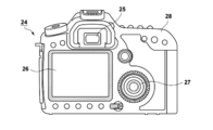
- FIG. 12A is a schematic view showing an example of the photoelectric conversion device according to the present embodiment.
- the photoelectric conversion device 1100 may include a viewfinder 1101, a rear display 1102, an operation unit 1103, and a housing 1104.
- the viewfinder 1101 may have a display device according to the present embodiment.
- the display device may display not only the image to be captured but also environmental information, imaging instructions, and the like.
- the environmental information may include the intensity of external light, the direction of external light, the moving speed of the subject, the possibility that the subject is shielded by a shield, and the like.
- the optimum timing for imaging is a short time, so it is better to display the information as soon as possible. Therefore, it is preferable to use a display device using the organic light emitting element of the present invention. This is because the organic light emitting element has a high response speed.
- a display device using an organic light emitting element can be more preferably used than these devices and liquid crystal display devices, which require a display speed.
- the photoelectric conversion device 1100 has an optical unit (not shown).
- the optical unit has a plurality of lenses and forms an image on an image sensor housed in the housing 1104.
- the focal point of a plurality of lenses can be adjusted by adjusting their relative positions. This operation can also be performed automatically.
- the display device may have a color filter having red, green, and blue.
- the red, green, and blue may be arranged in a delta arrangement.
- the display device may be used as a display unit of a mobile terminal. In that case, it may have both a display function and an operation function.
- Examples of the mobile terminal include a mobile phone such as a smartphone, a tablet, a head-mounted display, and the like.
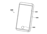
- FIG. 12B is a schematic view showing another example of the electronic device according to the present embodiment.
- the electronic device 1200 has a display unit 1201, an operation unit 1202, and a housing 1203.
- the housing 1203 may include a circuit, a printed circuit board having the circuit, a battery, and a communication unit.
- the operation unit 1202 may be a button or a touch panel type reaction unit.
- the operation unit may be a biometric recognition unit that recognizes a fingerprint and releases the lock.
- An electronic device having a communication unit can also be called a communication device.
- FIG. 13A and 13B are schematic views showing an example of a display device according to the present embodiment.
- FIG. 13A is a display device such as a television monitor or a PC monitor.
- the display device 1300 has a frame 1301 and a display unit 1302.
- the light emitting device according to the present embodiment may be used for the display unit 1302.
- the display device 1300 has a base 1303 that supports the frame 1301 and the display unit 1302.
- the base 1303 is not limited to the form shown in FIG. 13A.
- the lower side of the frame 1301 may also serve as the base. Further, the frame 1301 and the display unit 1302 may be bent.
- the radius of curvature may be 5000 mm or more and 6000 mm or less.
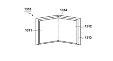
- FIG. 13B is a schematic view showing another example of the display device according to the present embodiment.
- the display device 1310 of FIG. 13B is a foldable display device, which is a so-called foldable display device.
- the display device 1310 has a first display unit 1311, a second display unit 1312, a housing 1313, and a bending point 1314.
- the first display unit 1311 and the second display unit 1312 may have a light emitting device according to the present embodiment.
- the first display unit 1311 and the second display unit 1312 may be a single display device having no joints.
- the first display unit 1311 and the second display unit 1312 can be separated by a bending point.
- the first display unit 1311 and the second display unit 1312 may display different images, or the first and second display units may display one image.
- FIG. 14A is a schematic view showing an example of the lighting device according to the present embodiment.
- the lighting device 1400 may include a housing 1401, a light source 1402, a circuit board 1403, an optical film 1404, and a light diffusing unit 1405.
- the light source may have the organic light emitting element according to the present embodiment.
- the optical filter may be a filter that improves the color rendering property of the light source.
- the light diffusing unit can effectively diffuse the light of the light source such as lighting up and deliver the light to a wide range.
- the optical filter and the light diffusing unit may be provided on the light emitting side of the illumination. If necessary, a cover may be provided on the outermost side.
- the lighting device is, for example, a device that illuminates the room.
- the illuminating device may emit white, neutral white, or any other color from blue to red. It may have a dimming circuit for dimming them.
- the lighting device may have the organic light emitting element of the present invention and a power supply circuit connected to the organic light emitting element.
- the power supply circuit is a circuit that converts an AC voltage into a DC voltage. Further, white has a color temperature of 4200 K, and neutral white has a color temperature of 5000 K.
- the illuminator may have a color filter.
- the lighting device according to the present embodiment may have a heat radiating unit.
- the heat radiating unit releases the heat inside the device to the outside of the device, and examples thereof include metals and liquid silicon having a high specific heat.
- FIG. 14B is a schematic view of an automobile which is an example of a moving body according to the present embodiment.
- the vehicle has a tail lamp, which is an example of a lamp.
- the automobile 1500 may have a tail lamp 1501 and may be in a form in which the tail lamp is turned on when a brake operation or the like is performed.
- the tail lamp 1501 may have an organic light emitting element according to the present embodiment.
- the tail lamp may have a protective member that protects the organic EL element.
- the protective member has a certain degree of high strength and may be made of any material as long as it is transparent, but it is preferably made of polycarbonate or the like.
- a flange carboxylic acid derivative, an acrylonitrile derivative, or the like may be mixed with the polycarbonate.
- the automobile 1500 may have a vehicle body 1503 and a window 1502 attached to the vehicle body 1503.
- the window may be a transparent display as long as it is not a window for checking the front and rear of the automobile.
- the transparent display may have the organic light emitting element according to the present embodiment.
- the constituent material such as the electrode of the organic light emitting element is composed of a transparent member.
- the moving body according to this embodiment may be a ship, an aircraft, a drone, or the like.
- the moving body may have an airframe and a lamp provided on the airframe.
- the lamp may emit light to indicate the position of the aircraft.
- the lamp has an organic light emitting element according to the present embodiment.
- FIGS. 15A-15C are application examples of the display device according to the embodiment of the present invention.
- the display device according to the embodiment of the present invention can be applied to an information display device such as a viewfinder of a camera, a head-mounted display, and smart glasses.
- FIG. 15A is a schematic configuration diagram of an example used as a viewfinder of an imaging device such as a camera.
- the display light 7 and the infrared light 8 are emitted from the display device 1, and the display light and the infrared light reach the user's eyeball 6 through the same optical member 22.
- the infrared light reflected by the user's eyeball 6 is converted into electrical information by an image pickup device 23 having an image pickup element, and the line of sight is detected based on the information.
- an image pickup element may be provided on the insulating layer of the display device 1 and used as the display image pickup device.
- FIG. 15B is an example of an imaging device such as a camera.
- the image pickup apparatus 24 includes a viewfinder 25, a display 26, an operation unit 27, and a housing 28.
- the display device of FIG. 15A is provided in the viewfinder 25.
- FIG. 15A shows an example in which the display light 7 and the infrared light 8 pass through the same optical member 22, different optical members may be provided for the display light and the infrared light. Further, instead of providing the image pickup device, an image pickup element may be provided on the substrate of the display device 1 and used as the display image pickup device.
- the detected line-of-sight information can be used for controlling a display device and various devices connected to the display device, such as camera focus control, display image resolution control, and button operation substitution.
- the display device has an image pickup device having a light receiving element, and may control the display image of the display device based on the user's line-of-sight information from the image pickup device.
- the display device determines a first visual field region to be watched by the user and a second visual field region other than the first visual field region based on the line-of-sight information.
- the first field of view area and the second field of view area may be determined by the control device of the display device, or may receive those determined by the external control device.
- the display resolution of the first field of view area may be controlled to be higher than the display resolution of the second field of view area. That is, the resolution of the second field of view may be lower than that of the first field of view.
- the display area has a first display area and a second display area different from the first display area, and the priority is given from the first display area and the second display area based on the line-of-sight information. Is determined in the high region.
- the first field of view area and the second field of view area may be determined by the control device of the display device, or may receive those determined by the external control device.
- the resolution of the high-priority region may be controlled higher than the resolution of the region other than the high-priority region. That is, the resolution of the region having a relatively low priority may be lowered.
- AI may be used to determine the first field of view area and the area with high priority.
- AI is a model configured to estimate the angle of the line of sight and the distance to the target object ahead of the line of sight from the image of the eyeball using the image of the eyeball and the direction in which the eyeball of the image was actually viewed as training data. It may be there.
- the AI program may be possessed by a display device, an imaging device, or an external device. If the external device has it, it is transmitted to the display device via communication.
- the display When the display is controlled based on the visual detection, it can be preferably applied to smart glasses having an image pickup device that images the outside. Smart glasses can display captured external information in real time.
- first imaging device having a light receiving element that receives infrared light
- second imaging device that has a light receiving element different from that of the first imaging device and for imaging the outside.
- the imaging resolution of the second imaging device may be controlled based on the line-of-sight information of the user of the first imaging device.
- the amount of information can be reduced by lowering the other areas as compared with the area where the image resolution is prioritized. Therefore, power consumption can be reduced and display delay can be reduced.
- the priority region may be the first imaging region, and the region having a lower priority than the first imaging region may be the second imaging region.
- FIG. 15C is a schematic view showing an example of smart glasses.
- the image pickup display device 29 represented by smart glasses has a control unit 30, a transparent display unit 31, and an external image pickup unit (not shown).
- both the display device and the external imaging device can be controlled based on the detected line-of-sight information, and power consumption and display delay can be reduced. For example, by lowering the display and imaging resolution of an area other than the area of the display area that the user is gazing at, the amount of information for both imaging and display can be reduced, and power consumption and display delay can be reduced.
- the visible light emitted by the infrared light emitting element is reduced from becoming leakage light of adjacent pixels, so that the display quality is reduced even when the size is reduced. It is possible to provide a display device in which the decrease in the amount of light is reduced.
Landscapes
- Engineering & Computer Science (AREA)
- Microelectronics & Electronic Packaging (AREA)
- Physics & Mathematics (AREA)
- Optics & Photonics (AREA)
- Multimedia (AREA)
- Signal Processing (AREA)
- Manufacturing & Machinery (AREA)
- Inorganic Chemistry (AREA)
- Chemical & Material Sciences (AREA)
- General Engineering & Computer Science (AREA)
- Life Sciences & Earth Sciences (AREA)
- Sustainable Development (AREA)
- Electroluminescent Light Sources (AREA)
- Devices For Indicating Variable Information By Combining Individual Elements (AREA)
Priority Applications (5)
| Application Number | Priority Date | Filing Date | Title |
|---|---|---|---|
| EP20882652.9A EP4033475A4 (en) | 2019-10-28 | 2020-10-16 | ORGANIC DEVICE, METHOD FOR PRODUCING THE SAME, DISPLAY DEVICE, PHOTOELECTRIC CONVERSION DEVICE, ELECTRONIC DEVICE, LIGHTING DEVICE AND MOBILE BODY |
| CN202510696567.5A CN120568980A (zh) | 2019-10-28 | 2020-10-16 | 有机装置及其制造方法、显示装置、光电转换装置、电子设备、照明装置和移动体 |
| CN202080075604.6A CN114616690B (zh) | 2019-10-28 | 2020-10-16 | 有机装置、制造方法、显示装置、电子设备和移动体 |
| KR1020227014382A KR102860292B1 (ko) | 2019-10-28 | 2020-10-16 | 유기 디바이스, 그 제조 방법, 표시장치, 광전변환 장치, 전자기기, 조명 장치 및 이동체 |
| US17/730,504 US12532604B2 (en) | 2019-10-28 | 2022-04-27 | Organic device, method of manufacturing the same, display device, photoelectric conversion device, electronic apparatus, illumination device, and moving body |
Applications Claiming Priority (4)
| Application Number | Priority Date | Filing Date | Title |
|---|---|---|---|
| JP2019195526 | 2019-10-28 | ||
| JP2019-195526 | 2019-10-28 | ||
| JP2020163887A JP7689419B2 (ja) | 2019-10-28 | 2020-09-29 | 有機デバイス、その製造方法、表示装置、光電変換装置、電子機器、照明装置および移動体 |
| JP2020-163887 | 2020-09-29 |
Related Child Applications (1)
| Application Number | Title | Priority Date | Filing Date |
|---|---|---|---|
| US17/730,504 Continuation US12532604B2 (en) | 2019-10-28 | 2022-04-27 | Organic device, method of manufacturing the same, display device, photoelectric conversion device, electronic apparatus, illumination device, and moving body |
Publications (1)
| Publication Number | Publication Date |
|---|---|
| WO2021085187A1 true WO2021085187A1 (ja) | 2021-05-06 |
Family
ID=75713531
Family Applications (1)
| Application Number | Title | Priority Date | Filing Date |
|---|---|---|---|
| PCT/JP2020/039132 Ceased WO2021085187A1 (ja) | 2019-10-28 | 2020-10-16 | 有機デバイス、その製造方法、表示装置、光電変換装置、電子機器、照明装置および移動体 |
Country Status (6)
| Country | Link |
|---|---|
| US (1) | US12532604B2 (https=) |
| EP (1) | EP4033475A4 (https=) |
| JP (2) | JP7689419B2 (https=) |
| KR (1) | KR102860292B1 (https=) |
| CN (2) | CN114616690B (https=) |
| WO (1) | WO2021085187A1 (https=) |
Cited By (1)
| Publication number | Priority date | Publication date | Assignee | Title |
|---|---|---|---|---|
| EP4266853A1 (en) * | 2022-04-20 | 2023-10-25 | Canon Kabushiki Kaisha | Light emitting apparatus, display device, photoelectric conversion device, electronic apparatus, and moving body |
Families Citing this family (11)
| Publication number | Priority date | Publication date | Assignee | Title |
|---|---|---|---|---|
| US11758786B2 (en) * | 2020-03-18 | 2023-09-12 | Boe Technology Group Co., Ltd. | Array substrate, fabricating method therefor and display panel |
| CN112952024B (zh) * | 2021-03-17 | 2026-04-14 | 京东方科技集团股份有限公司 | 有机电致发光器件及显示面板 |
| JP7695141B2 (ja) * | 2021-07-28 | 2025-06-18 | キヤノン株式会社 | 有機デバイス、画像形成装置、表示装置、光電変換装置、電子機器、照明装置、移動体、および、ウェアラブルデバイス |
| JP7830057B2 (ja) * | 2021-09-09 | 2026-03-16 | キヤノン株式会社 | 有機発光装置、それを有する表示装置、電子機器、及び有機発光装置の製造方法 |
| JP7700607B2 (ja) * | 2021-09-29 | 2025-07-01 | セイコーエプソン株式会社 | 電気光学装置および電子機器 |
| JP7778518B2 (ja) * | 2021-10-07 | 2025-12-02 | キヤノン株式会社 | 有機発光素子、表示装置、光電変換装置、電子機器、照明装置、および移動体 |
| JP2023088115A (ja) * | 2021-12-14 | 2023-06-26 | キヤノン株式会社 | 発光装置、表示装置、光電変換装置、電子機器、照明装置、および、移動体 |
| JP7709423B2 (ja) * | 2022-04-20 | 2025-07-16 | キヤノン株式会社 | 発光装置、表示装置、光電変換装置、電子機器および移動体 |
| JP2023165556A (ja) | 2022-05-06 | 2023-11-16 | キヤノン株式会社 | 発光装置、発光装置の製造方法、表示装置、光電変換装置、電子機器、照明装置、移動体、および、ウェアラブルデバイス |
| JP2024077313A (ja) | 2022-11-28 | 2024-06-07 | キヤノン株式会社 | 有機デバイスおよびそれを用いた表示装置 |
| JP2024127527A (ja) * | 2023-03-09 | 2024-09-20 | キヤノン株式会社 | 発光装置およびその製造方法 |
Citations (9)
| Publication number | Priority date | Publication date | Assignee | Title |
|---|---|---|---|---|
| JP2008210740A (ja) * | 2007-02-28 | 2008-09-11 | Seiko Epson Corp | 表示装置 |
| JP2010050014A (ja) * | 2008-08-25 | 2010-03-04 | Seiko Epson Corp | 発光装置および電子機器 |
| JP2010244693A (ja) * | 2009-04-01 | 2010-10-28 | Seiko Epson Corp | 有機el装置および有機el装置の製造方法、ならびに電子機器 |
| JP2014222592A (ja) * | 2013-05-13 | 2014-11-27 | 株式会社ジャパンディスプレイ | 表示装置 |
| JP2015011913A (ja) * | 2013-07-01 | 2015-01-19 | セイコーエプソン株式会社 | 発光装置および電子機器 |
| JP2015197994A (ja) * | 2014-04-01 | 2015-11-09 | セイコーエプソン株式会社 | 発光装置の製造方法、発光装置、及び電子機器 |
| JP2017107887A (ja) | 2017-03-27 | 2017-06-15 | セイコーエプソン株式会社 | 電気光学装置及び電子機器 |
| JP2019195526A (ja) | 2018-05-10 | 2019-11-14 | 株式会社高尾 | 弾球遊技機 |
| JP2020163887A (ja) | 2019-03-28 | 2020-10-08 | ピジョン株式会社 | ベルトカバーおよび座席装置 |
Family Cites Families (26)
| Publication number | Priority date | Publication date | Assignee | Title |
|---|---|---|---|---|
| JP4573672B2 (ja) * | 2005-02-28 | 2010-11-04 | 三洋電機株式会社 | 有機elパネル |
| JP4655942B2 (ja) * | 2006-01-16 | 2011-03-23 | セイコーエプソン株式会社 | 発光装置、発光装置の製造方法および電子機器 |
| JP2007287354A (ja) * | 2006-04-12 | 2007-11-01 | Hitachi Displays Ltd | 有機el表示装置 |
| JP4678421B2 (ja) * | 2008-05-16 | 2011-04-27 | ソニー株式会社 | 表示装置 |
| JP2010020926A (ja) | 2008-07-08 | 2010-01-28 | Sony Corp | 表示装置 |
| KR20130016938A (ko) * | 2011-08-09 | 2013-02-19 | 삼성디스플레이 주식회사 | 유기 발광 표시 장치 및 그 제조 방법 |
| JP5832210B2 (ja) * | 2011-09-16 | 2015-12-16 | キヤノン株式会社 | 有機el素子 |
| JP5963458B2 (ja) * | 2012-01-31 | 2016-08-03 | キヤノン株式会社 | 発光装置、画像形成装置及び撮像装置 |
| JP5998626B2 (ja) | 2012-05-15 | 2016-09-28 | セイコーエプソン株式会社 | 電気光学装置および電子機器 |
| JP6201442B2 (ja) * | 2013-06-17 | 2017-09-27 | セイコーエプソン株式会社 | 電気光学装置、電気光学装置の製造方法、電子機器 |
| JP2015041969A (ja) * | 2013-08-23 | 2015-03-02 | ソニー株式会社 | 画像取得装置及び画像取得方法、並びに情報配信システム。 |
| CN103456765B (zh) * | 2013-09-10 | 2015-09-16 | 深圳市华星光电技术有限公司 | 有源式有机电致发光器件背板及其制作方法 |
| JP6576937B2 (ja) * | 2014-09-25 | 2019-09-18 | オリンパス株式会社 | 照明装置及び表示装置 |
| CN107170762B (zh) * | 2017-06-16 | 2019-04-30 | 武汉华星光电半导体显示技术有限公司 | Oled显示面板及其制作方法 |
| JP6957294B2 (ja) * | 2017-09-28 | 2021-11-02 | キヤノン株式会社 | 表示装置、電子機器、及び表示装置の製造方法 |
| JP2019110007A (ja) * | 2017-12-18 | 2019-07-04 | 株式会社ジャパンディスプレイ | 有機el表示装置 |
| EP3561893B1 (en) * | 2018-04-26 | 2022-06-15 | Canon Kabushiki Kaisha | Organic device and method of manufacturing the same |
| JP7075292B2 (ja) * | 2018-06-21 | 2022-05-25 | キヤノン株式会社 | 有機デバイス、表示装置、撮像装置、照明装置、移動体用灯具、および、移動体 |
| JP7115276B2 (ja) * | 2018-12-10 | 2022-08-09 | トヨタ自動車株式会社 | 運転支援装置、ウェアラブル装置、運転支援システム、運転支援方法およびプログラム |
| US11380864B2 (en) * | 2019-02-13 | 2022-07-05 | Canon Kabushiki Kaisha | Electronic device, display apparatus, photoelectric conversion apparatus, electronic apparatus, illumination apparatus, and moving object |
| JP7245088B2 (ja) * | 2019-03-20 | 2023-03-23 | キヤノン株式会社 | 有機デバイス、表示装置、撮像装置、照明装置および移動体 |
| JP7304734B2 (ja) * | 2019-05-07 | 2023-07-07 | キヤノン株式会社 | 有機デバイス、表示装置、撮像装置、照明装置および移動体 |
| JP7308659B2 (ja) | 2019-05-27 | 2023-07-14 | キヤノン株式会社 | 表示装置、その製造方法および電気装置 |
| JP7341798B2 (ja) * | 2019-08-30 | 2023-09-11 | キヤノン株式会社 | 半導体装置、発光装置、表示装置、撮像装置、電子機器、照明装置、及び移動体 |
| JP7321049B2 (ja) * | 2019-10-11 | 2023-08-04 | キヤノン株式会社 | 発光装置、表示装置、光電変換装置、電子機器、照明装置および移動体 |
| JP7198250B2 (ja) * | 2020-10-12 | 2022-12-28 | キヤノン株式会社 | 表示装置 |
-
2020
- 2020-09-29 JP JP2020163887A patent/JP7689419B2/ja active Active
- 2020-10-16 KR KR1020227014382A patent/KR102860292B1/ko active Active
- 2020-10-16 CN CN202080075604.6A patent/CN114616690B/zh active Active
- 2020-10-16 EP EP20882652.9A patent/EP4033475A4/en active Pending
- 2020-10-16 WO PCT/JP2020/039132 patent/WO2021085187A1/ja not_active Ceased
- 2020-10-16 CN CN202510696567.5A patent/CN120568980A/zh active Pending
-
2022
- 2022-04-27 US US17/730,504 patent/US12532604B2/en active Active
-
2025
- 2025-05-26 JP JP2025087404A patent/JP2025116076A/ja active Pending
Patent Citations (9)
| Publication number | Priority date | Publication date | Assignee | Title |
|---|---|---|---|---|
| JP2008210740A (ja) * | 2007-02-28 | 2008-09-11 | Seiko Epson Corp | 表示装置 |
| JP2010050014A (ja) * | 2008-08-25 | 2010-03-04 | Seiko Epson Corp | 発光装置および電子機器 |
| JP2010244693A (ja) * | 2009-04-01 | 2010-10-28 | Seiko Epson Corp | 有機el装置および有機el装置の製造方法、ならびに電子機器 |
| JP2014222592A (ja) * | 2013-05-13 | 2014-11-27 | 株式会社ジャパンディスプレイ | 表示装置 |
| JP2015011913A (ja) * | 2013-07-01 | 2015-01-19 | セイコーエプソン株式会社 | 発光装置および電子機器 |
| JP2015197994A (ja) * | 2014-04-01 | 2015-11-09 | セイコーエプソン株式会社 | 発光装置の製造方法、発光装置、及び電子機器 |
| JP2017107887A (ja) | 2017-03-27 | 2017-06-15 | セイコーエプソン株式会社 | 電気光学装置及び電子機器 |
| JP2019195526A (ja) | 2018-05-10 | 2019-11-14 | 株式会社高尾 | 弾球遊技機 |
| JP2020163887A (ja) | 2019-03-28 | 2020-10-08 | ピジョン株式会社 | ベルトカバーおよび座席装置 |
Non-Patent Citations (1)
| Title |
|---|
| See also references of EP4033475A4 |
Cited By (4)
| Publication number | Priority date | Publication date | Assignee | Title |
|---|---|---|---|---|
| EP4266853A1 (en) * | 2022-04-20 | 2023-10-25 | Canon Kabushiki Kaisha | Light emitting apparatus, display device, photoelectric conversion device, electronic apparatus, and moving body |
| KR20230149726A (ko) * | 2022-04-20 | 2023-10-27 | 캐논 가부시끼가이샤 | 발광장치, 표시장치, 광전 변환장치, 전자기기, 및 이동체 |
| US12433126B2 (en) | 2022-04-20 | 2025-09-30 | Canon Kabushiki Kaisha | Light emitting apparatus, display device, photoelectric conversion device, electronic apparatus, and moving body |
| KR102923612B1 (ko) * | 2022-04-20 | 2026-02-05 | 캐논 가부시끼가이샤 | 발광장치, 표시장치, 광전 변환장치, 전자기기, 및 이동체 |
Also Published As
| Publication number | Publication date |
|---|---|
| KR102860292B1 (ko) | 2025-09-17 |
| CN114616690B (zh) | 2025-06-10 |
| CN120568980A (zh) | 2025-08-29 |
| EP4033475A4 (en) | 2023-10-18 |
| JP2021072282A (ja) | 2021-05-06 |
| US20220255042A1 (en) | 2022-08-11 |
| EP4033475A1 (en) | 2022-07-27 |
| JP2025116076A (ja) | 2025-08-07 |
| KR20220075370A (ko) | 2022-06-08 |
| US12532604B2 (en) | 2026-01-20 |
| JP7689419B2 (ja) | 2025-06-06 |
| CN114616690A (zh) | 2022-06-10 |
Similar Documents
| Publication | Publication Date | Title |
|---|---|---|
| JP7689419B2 (ja) | 有機デバイス、その製造方法、表示装置、光電変換装置、電子機器、照明装置および移動体 | |
| US12279476B2 (en) | Light emitting device, exposure system, imaging display device, imaging device, electronic device, and lighting device | |
| JP2021068501A (ja) | 発光デバイス、表示装置、光電変換装置、電子機器、照明装置および移動体 | |
| JP2021136208A (ja) | 発光装置、表示装置、露光システム、及び表示撮像装置 | |
| JP7418086B2 (ja) | 半導体装置、表示装置、表示撮像装置、及び光電変換装置 | |
| JP7528016B2 (ja) | 発光装置、表示装置、撮像装置、及び電子機器 | |
| JP2021158260A (ja) | 電子デバイスおよびその製造方法、電子装置ならびに移動体 | |
| JP2022022910A (ja) | 有機デバイス、表示装置、光電変換装置、電子機器、照明装置、移動体用の灯具および移動体 | |
| JP2022022875A (ja) | 有機デバイス、表示装置、光電変換装置、電子機器、照明装置、移動体用の灯具および移動体 | |
| JP2024129092A (ja) | 有機発光装置、表示装置、及び電子機器 | |
| US12446439B2 (en) | Light emitting device, manufacturing method of light emitting device, display device, photoelectric conversion device, electronic apparatus, illumination device, moving body, and wearable device | |
| US20250311541A1 (en) | Organic light-emitting element | |
| JP7395271B2 (ja) | 発光装置、表示装置、及び発光装置の製造方法 | |
| JP2021125451A (ja) | 発光装置、表示撮像装置、及び電子機器 | |
| TWI892109B (zh) | 發光裝置、顯示裝置、光電轉換裝置、電子裝置及發光裝置之製造方法 | |
| US20250380593A1 (en) | Light emitting device and method for producing same | |
| US20240244872A1 (en) | Light emitting element | |
| JP2025005678A (ja) | 発光素子、発光装置、それを有する撮像装置、電子機器、照明装置、移動体 | |
| WO2025204826A1 (ja) | 発光装置、表示装置、撮像装置及び電子機器 | |
| JP2025084054A (ja) | 発光装置、表示装置、光電変換装置、電子機器、照明装置及び移動体 | |
| KR20240173690A (ko) | 발광장치, 표시장치, 광전 변환장치, 전자기기, 및 웨어러블 디바이스 | |
| JP2025076141A (ja) | 発光装置、画像形成装置、表示装置、光電変換装置、電子機器、照明装置、移動体、および、ウェアラブルデバイス | |
| JP2023164291A (ja) | 発光装置及びその製造方法、表示装置、光電変換装置、電子機器、照明装置、並びに移動体 | |
| JP2025149106A (ja) | 発光装置、表示装置、撮像装置及び電子機器 | |
| WO2025109982A1 (ja) | 発光装置、表示装置、光電変換装置、電子機器、照明装置及び移動体 |
Legal Events
| Date | Code | Title | Description |
|---|---|---|---|
| 121 | Ep: the epo has been informed by wipo that ep was designated in this application |
Ref document number: 20882652 Country of ref document: EP Kind code of ref document: A1 |
|
| ENP | Entry into the national phase |
Ref document number: 20227014382 Country of ref document: KR Kind code of ref document: A |
|
| ENP | Entry into the national phase |
Ref document number: 2020882652 Country of ref document: EP Effective date: 20220421 |
|
| NENP | Non-entry into the national phase |
Ref country code: DE |
|
| WWG | Wipo information: grant in national office |
Ref document number: 202080075604.6 Country of ref document: CN |