WO2021075353A1 - 半導体集積回路装置 - Google Patents
半導体集積回路装置 Download PDFInfo
- Publication number
- WO2021075353A1 WO2021075353A1 PCT/JP2020/038192 JP2020038192W WO2021075353A1 WO 2021075353 A1 WO2021075353 A1 WO 2021075353A1 JP 2020038192 W JP2020038192 W JP 2020038192W WO 2021075353 A1 WO2021075353 A1 WO 2021075353A1
- Authority
- WO
- WIPO (PCT)
- Prior art keywords
- power supply
- wiring
- local
- supply wiring
- metal
- Prior art date
- Legal status (The legal status is an assumption and is not a legal conclusion. Google has not performed a legal analysis and makes no representation as to the accuracy of the status listed.)
- Ceased
Links
Images






Classifications
-
- H—ELECTRICITY
- H10—SEMICONDUCTOR DEVICES; ELECTRIC SOLID-STATE DEVICES NOT OTHERWISE PROVIDED FOR
- H10D—INORGANIC ELECTRIC SEMICONDUCTOR DEVICES
- H10D89/00—Aspects of integrated devices not covered by groups H10D84/00 - H10D88/00
- H10D89/10—Integrated device layouts
-
- H—ELECTRICITY
- H10—SEMICONDUCTOR DEVICES; ELECTRIC SOLID-STATE DEVICES NOT OTHERWISE PROVIDED FOR
- H10W—GENERIC PACKAGES, INTERCONNECTIONS, CONNECTORS OR OTHER CONSTRUCTIONAL DETAILS OF DEVICES COVERED BY CLASS H10
- H10W20/00—Interconnections in chips, wafers or substrates
- H10W20/40—Interconnections external to wafers or substrates, e.g. back-end-of-line [BEOL] metallisations or vias connecting to gate electrodes
- H10W20/41—Interconnections external to wafers or substrates, e.g. back-end-of-line [BEOL] metallisations or vias connecting to gate electrodes characterised by their conductive parts
- H10W20/435—Cross-sectional shapes or dispositions of interconnections
-
- H—ELECTRICITY
- H10—SEMICONDUCTOR DEVICES; ELECTRIC SOLID-STATE DEVICES NOT OTHERWISE PROVIDED FOR
- H10W—GENERIC PACKAGES, INTERCONNECTIONS, CONNECTORS OR OTHER CONSTRUCTIONAL DETAILS OF DEVICES COVERED BY CLASS H10
- H10W20/00—Interconnections in chips, wafers or substrates
- H10W20/20—Interconnections within wafers or substrates, e.g. through-silicon vias [TSV]
-
- H—ELECTRICITY
- H10—SEMICONDUCTOR DEVICES; ELECTRIC SOLID-STATE DEVICES NOT OTHERWISE PROVIDED FOR
- H10W—GENERIC PACKAGES, INTERCONNECTIONS, CONNECTORS OR OTHER CONSTRUCTIONAL DETAILS OF DEVICES COVERED BY CLASS H10
- H10W20/00—Interconnections in chips, wafers or substrates
- H10W20/40—Interconnections external to wafers or substrates, e.g. back-end-of-line [BEOL] metallisations or vias connecting to gate electrodes
- H10W20/41—Interconnections external to wafers or substrates, e.g. back-end-of-line [BEOL] metallisations or vias connecting to gate electrodes characterised by their conductive parts
- H10W20/427—Power or ground buses
-
- H—ELECTRICITY
- H10—SEMICONDUCTOR DEVICES; ELECTRIC SOLID-STATE DEVICES NOT OTHERWISE PROVIDED FOR
- H10W—GENERIC PACKAGES, INTERCONNECTIONS, CONNECTORS OR OTHER CONSTRUCTIONAL DETAILS OF DEVICES COVERED BY CLASS H10
- H10W70/00—Package substrates; Interposers; Redistribution layers [RDL]
- H10W70/60—Insulating or insulated package substrates; Interposers; Redistribution layers
- H10W70/611—Insulating or insulated package substrates; Interposers; Redistribution layers for connecting multiple chips together
-
- H—ELECTRICITY
- H10—SEMICONDUCTOR DEVICES; ELECTRIC SOLID-STATE DEVICES NOT OTHERWISE PROVIDED FOR
- H10W—GENERIC PACKAGES, INTERCONNECTIONS, CONNECTORS OR OTHER CONSTRUCTIONAL DETAILS OF DEVICES COVERED BY CLASS H10
- H10W70/00—Package substrates; Interposers; Redistribution layers [RDL]
- H10W70/60—Insulating or insulated package substrates; Interposers; Redistribution layers
- H10W70/62—Insulating or insulated package substrates; Interposers; Redistribution layers characterised by their interconnections
- H10W70/65—Shapes or dispositions of interconnections
-
- B—PERFORMING OPERATIONS; TRANSPORTING
- B82—NANOTECHNOLOGY
- B82Y—SPECIFIC USES OR APPLICATIONS OF NANOSTRUCTURES; MEASUREMENT OR ANALYSIS OF NANOSTRUCTURES; MANUFACTURE OR TREATMENT OF NANOSTRUCTURES
- B82Y10/00—Nanotechnology for information processing, storage or transmission, e.g. quantum computing or single electron logic
-
- H—ELECTRICITY
- H10—SEMICONDUCTOR DEVICES; ELECTRIC SOLID-STATE DEVICES NOT OTHERWISE PROVIDED FOR
- H10D—INORGANIC ELECTRIC SEMICONDUCTOR DEVICES
- H10D30/00—Field-effect transistors [FET]
- H10D30/40—FETs having zero-dimensional [0D], one-dimensional [1D] or two-dimensional [2D] charge carrier gas channels
- H10D30/43—FETs having zero-dimensional [0D], one-dimensional [1D] or two-dimensional [2D] charge carrier gas channels having one-dimensional [1D] charge carrier gas channels, e.g. quantum wire FETs or transistors having 1D quantum-confined channels
-
- H—ELECTRICITY
- H10—SEMICONDUCTOR DEVICES; ELECTRIC SOLID-STATE DEVICES NOT OTHERWISE PROVIDED FOR
- H10D—INORGANIC ELECTRIC SEMICONDUCTOR DEVICES
- H10D30/00—Field-effect transistors [FET]
- H10D30/60—Insulated-gate field-effect transistors [IGFET]
- H10D30/62—Fin field-effect transistors [FinFET]
-
- H—ELECTRICITY
- H10—SEMICONDUCTOR DEVICES; ELECTRIC SOLID-STATE DEVICES NOT OTHERWISE PROVIDED FOR
- H10D—INORGANIC ELECTRIC SEMICONDUCTOR DEVICES
- H10D30/00—Field-effect transistors [FET]
- H10D30/60—Insulated-gate field-effect transistors [IGFET]
- H10D30/67—Thin-film transistors [TFT]
- H10D30/6729—Thin-film transistors [TFT] characterised by the electrodes
- H10D30/673—Thin-film transistors [TFT] characterised by the electrodes characterised by the shapes, relative sizes or dispositions of the gate electrodes
- H10D30/6735—Thin-film transistors [TFT] characterised by the electrodes characterised by the shapes, relative sizes or dispositions of the gate electrodes having gates fully surrounding the channels, e.g. gate-all-around
-
- H—ELECTRICITY
- H10—SEMICONDUCTOR DEVICES; ELECTRIC SOLID-STATE DEVICES NOT OTHERWISE PROVIDED FOR
- H10D—INORGANIC ELECTRIC SEMICONDUCTOR DEVICES
- H10D30/00—Field-effect transistors [FET]
- H10D30/60—Insulated-gate field-effect transistors [IGFET]
- H10D30/67—Thin-film transistors [TFT]
- H10D30/6757—Thin-film transistors [TFT] characterised by the structure of the channel, e.g. transverse or longitudinal shape or doping profile
-
- H—ELECTRICITY
- H10—SEMICONDUCTOR DEVICES; ELECTRIC SOLID-STATE DEVICES NOT OTHERWISE PROVIDED FOR
- H10D—INORGANIC ELECTRIC SEMICONDUCTOR DEVICES
- H10D62/00—Semiconductor bodies, or regions thereof, of devices having potential barriers
- H10D62/10—Shapes, relative sizes or dispositions of the regions of the semiconductor bodies; Shapes of the semiconductor bodies
- H10D62/117—Shapes of semiconductor bodies
- H10D62/118—Nanostructure semiconductor bodies
- H10D62/119—Nanowire, nanosheet or nanotube semiconductor bodies
- H10D62/121—Nanowire, nanosheet or nanotube semiconductor bodies oriented parallel to substrates
-
- H—ELECTRICITY
- H10—SEMICONDUCTOR DEVICES; ELECTRIC SOLID-STATE DEVICES NOT OTHERWISE PROVIDED FOR
- H10D—INORGANIC ELECTRIC SEMICONDUCTOR DEVICES
- H10D84/00—Integrated devices formed in or on semiconductor substrates that comprise only semiconducting layers, e.g. on Si wafers or on GaAs-on-Si wafers
- H10D84/90—Masterslice integrated circuits
- H10D84/903—Masterslice integrated circuits comprising field effect technology
- H10D84/907—CMOS gate arrays
-
- H—ELECTRICITY
- H10—SEMICONDUCTOR DEVICES; ELECTRIC SOLID-STATE DEVICES NOT OTHERWISE PROVIDED FOR
- H10D—INORGANIC ELECTRIC SEMICONDUCTOR DEVICES
- H10D84/00—Integrated devices formed in or on semiconductor substrates that comprise only semiconducting layers, e.g. on Si wafers or on GaAs-on-Si wafers
- H10D84/90—Masterslice integrated circuits
- H10D84/903—Masterslice integrated circuits comprising field effect technology
- H10D84/907—CMOS gate arrays
- H10D84/968—Macro-architecture
- H10D84/974—Layout specifications, i.e. inner core regions
- H10D84/981—Power supply lines
-
- H—ELECTRICITY
- H10—SEMICONDUCTOR DEVICES; ELECTRIC SOLID-STATE DEVICES NOT OTHERWISE PROVIDED FOR
- H10W—GENERIC PACKAGES, INTERCONNECTIONS, CONNECTORS OR OTHER CONSTRUCTIONAL DETAILS OF DEVICES COVERED BY CLASS H10
- H10W20/00—Interconnections in chips, wafers or substrates
- H10W20/01—Manufacture or treatment
- H10W20/031—Manufacture or treatment of conductive parts of the interconnections
- H10W20/0698—Local interconnections
Definitions
- the present disclosure relates to a semiconductor integrated circuit device including a standard cell.
- the standard cell method is known as a method for forming a semiconductor integrated circuit on a semiconductor substrate.
- a basic unit having a specific logical function for example, an inverter, a latch, a flip-flop, a full adder, etc.
- a plurality of standard cells are arranged on a semiconductor substrate. Then, it is a method of designing an LSI chip by connecting these standard cells with wiring.
- the standard cell is provided with an embedded wiring (Buried Interconnect) layer instead of the power supply wiring provided in the metal wiring layer formed on the upper layer of the transistor as in the conventional case. It has been proposed to use embedded power wiring (BPR: Buried Power Rail), which is the power wiring provided.
- BPR Buried Power Rail
- a power supply wiring is configured by an embedded power supply wiring, a transistor source is connected to the embedded power supply wiring, and further, a power supply wiring provided in an upper layer wiring layer is connected.
- the configuration is disclosed.
- Patent Document 1 Although the embedded power supply wiring is used as the power supply wiring of the standard cell, it is necessary to provide the power supply wiring in the upper wiring layer for each embedded power supply wiring. Therefore, the area where the signal wiring is laid in the upper wiring layer is reduced, which hinders the high integration of the semiconductor integrated circuit device.
- the purpose of the present disclosure is to secure an area for laying signal wiring in a power supply wiring structure for supplying power to a standard cell, and to realize high integration and small area of a semiconductor integrated circuit device.
- the semiconductor integrated circuit apparatus includes standard cells arranged in the first direction, and a plurality of cell rows arranged side by side in the second direction perpendicular to the first direction.
- the local power supply is formed in a metal wiring layer above the local wiring layer, extends in the first direction, and is arranged at a second predetermined interval larger than the first predetermined interval in the second direction. It is provided with a plurality of metal power supply wirings connected to the wiring.
- a plurality of embedded power supply wirings extending in the first direction are arranged at predetermined intervals in the second direction.
- a local power supply wiring extending in the second direction is connected to a plurality of embedded power supply wirings.
- a plurality of metal power supply wirings extending in the first direction are formed in the metal wiring layer above the local power supply wiring layer, and the plurality of metal power supply wirings are connected to the local power supply wiring.
- the semiconductor integrated circuit apparatus includes standard cells arranged in the first direction, and a plurality of cell rows arranged side by side in the second direction perpendicular to the first direction.
- the metal power supply wiring is connected by a plurality of connecting portions provided at a second predetermined interval larger than the first predetermined interval in the second direction.
- a plurality of embedded power supply wirings extending in the first direction are arranged at predetermined intervals in the second direction.
- a local power supply wiring extending in the second direction is connected to a plurality of embedded power supply wirings.
- a metal power supply wiring extending in the second direction is formed in the metal wiring layer above the local wiring layer, and the metal power supply wiring is formed by a plurality of connections arranged at predetermined intervals in the second direction to provide a local power supply. It is connected to the wiring.
- This configuration eliminates the need to provide metal wiring for each of the plurality of embedded power supply wirings, and the metal power supply wirings are a plurality of connections arranged at intervals larger than the arrangement intervals of the plurality of embedded power supply wirings in the second direction. It is connected to the local wiring by the part. As a result, it is possible to secure a larger area for laying the signal wiring in the metal wiring layer. Therefore, the area of the semiconductor integrated circuit can be reduced.
- the semiconductor integrated circuit device includes standard cells arranged in the first direction, and a plurality of cell rows arranged side by side in the second direction perpendicular to the first direction.
- the embedded power supply wiring which is formed in the embedded wiring layer, extends in the second direction, has an overlap with the local power supply wiring in a plan view, and is connected to the local power supply wiring, and the first It is formed in a second metal wiring layer which is an upper layer of one metal wiring layer, extends in the second direction, includes the local power supply wiring and an upper metal power supply wiring having an overlap in a plan view, and the local power supply.
- the wiring and the upper metal power supply wiring are connected only in the cell rows at both ends in the second direction of the plurality of cell rows.
- a plurality of metal power supply wirings extending in the first direction are arranged at predetermined intervals in the second direction.
- the local power supply wiring extending in the second direction is connected to a plurality of metal power supply wirings.
- the embedded power supply wiring extending in the second direction overlaps the local power supply wiring in a plan view and is connected to the local power supply wiring.
- An upper metal power supply wiring extending in the second direction is formed in the metal wiring layer above the plurality of metal power supply wirings, and the upper metal power supply wiring is connected to the local power supply wiring only in the cell rows at both ends in the second direction. It is connected. With this configuration, the power supply can be strengthened by the local power supply wiring and the embedded power supply wiring connected to each other.
- the upper metal power supply wiring is connected to the local power supply wiring only in the cell rows at both ends in the second direction, it is possible to secure a larger area for laying the signal wiring in the metal wiring layer. Therefore, the area of the semiconductor integrated circuit can be reduced.
- the power supply wiring structure for supplying power to the standard cell it is possible to secure an area for laying the signal wiring and realize high integration and small area of the semiconductor integrated circuit device.
- Layout example of the circuit block included in the semiconductor integrated circuit device according to the first embodiment (A) and (b) are cross-sectional views of the circuit block of FIG. Plan view showing an example of the layout structure of the power tap cell (A) and (b) are cross-sectional views of the power tap cell of FIG.
- Layout example of the circuit block related to the modified example is a plan view showing the layout structure of the VDD connection terminal cell
- (b) is a plan view showing the layout structure of the VSS connection terminal cell.
- Layout example of the circuit block included in the semiconductor integrated circuit device according to the second embodiment (A) and (b) are cross-sectional views of the circuit block of FIG.
- Layout example of the circuit block included in the semiconductor integrated circuit device according to the third embodiment (A) and (b) are cross-sectional views of the circuit block of FIG. It is a figure which shows the example of the layout structure of a power tap cell, (a) is a plan view, (b) is a sectional view.
- the semiconductor integrated circuit device comprises a plurality of standard cells (as appropriate herein, simply referred to as cells), of which at least a portion of the plurality of standard cells is, for example, a nanosheet FET.
- FieldEffectTransistor shall be provided.
- the nanosheet FET is an FET using a thin sheet (nanosheet) through which an electric current flows. Nanosheets are made of, for example, silicon. Further, in the present disclosure, a semiconductor layer portion formed at both ends of the nanosheet and forming a terminal serving as a source or drain of the nanosheet FET is referred to as a “pad”.
- VDD and VVSS indicate the power supply voltage or the power supply itself.
- the horizontal direction of the drawing is the X direction (corresponding to the first direction)
- the vertical direction of the drawing is the Y direction (corresponding to the second direction)
- the direction perpendicular to the substrate surface is defined. It is in the Z direction.
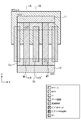
- FIG. 1 is an example of a layout of a circuit block included in the semiconductor integrated circuit apparatus according to the first embodiment
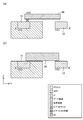
- FIG. 2A is a cross-sectional view taken along the line AA'of FIG. 1
- FIG. 2B is FIG. It is sectional drawing in line BB'.
- a plurality of cell row CRs including standard cells C arranged in the X direction are arranged side by side in the Y direction.
- the standard cell C includes, for example, a nanosheet FET.
- the plurality of cell rows CR are arranged upside down (inverted in the Y direction) every other row.
- the power supply wiring 3 for supplying the power supply voltage VDD and the power supply wiring 4 for supplying the power supply voltage VSS are alternately arranged between the cell rows CR.
- the power supply wirings 3 and 4 are so-called embedded power supply wirings (BPR: Buried Power Rail) formed in the embedded wiring layer.
- BPR Buried Power Rail
- the power supply voltages VDD and VSS are supplied from the power supply wirings 3 and 4 arranged at the top and bottom of the drawing.
- power tap cell groups 2a, 2b, 2c including a plurality of power tap cells 1 are arranged at equal intervals in the X direction.
- the power tap cell groups 2a, 2b, and 2c each include a plurality of power tap cells 1 located at the same position in the X direction.
- a local wiring extending in the Y direction is formed in the power tap cell 1.
- the local wiring is wiring formed in the local wiring layer in contact with the source and drain of the transistor included in the standard cell C.
- the power tap cells 1 are continuously arranged adjacent to each other in the Y direction, so that local power supply wirings 5 and 6 extending in the Y direction are formed in the circuit block.
- the local power supply wiring 5 is connected to the power supply wiring 3 for supplying VDD in the power supply tap cell 1 via vias.
- the local power supply wiring 6 is connected to the power supply wiring 4 for supplying VSS in the power supply tap cell 1 via vias.
- Metal power supply wirings 7 and 8 extending in the X direction are formed in the M4 wiring layer (the fourth metal wiring layer from the bottom).
- the metal power supply wiring 7 is connected to the local power supply wiring 5 via M1 to M3 wirings and vias.
- the metal power supply wiring 8 is connected to the local power supply wiring 6 via M1 to M3 wirings and vias. That is, VDD is supplied from the metal power supply wiring 7 to the power supply wiring 3 via the local power supply wiring 5.
- VSS is supplied from the metal power supply wiring 8 to the power supply wiring 4 via the local power supply wiring 6.
- FIG. 3 is a plan view showing an example of the layout structure of the power tap cell 1
- FIGS. 4 (a) and 4 (b) are cross-sectional views in the vertical direction in a plan view.
- FIG. 4A is a cross section of line AA'of FIG. 3
- FIG. 4B is a cross section of line BB'of FIG.
- FIG. 3 shows the cell frame CL of the power tap cell.
- FIG. 5 is a plan view showing an example of the layout structure of the inverter cell as an example of the cell C
- FIGS. 6A and 6B are cross-sectional views in the vertical direction in a plan view.
- 6 (a) is a cross section of line AA'of FIG. 5
- FIG. 6 (b) is a cross section of line BB' of FIG.
- power supply wirings 11 and 12 extending in the X direction are provided at both ends of the inverter cell in the Y direction, respectively.
- Both the power supply wirings 11 and 12 are embedded power supply wirings (BPR) formed in the embedded wiring layer.
- the power supply wiring 11 supplies the power supply voltage VDD
- the power supply wiring 12 supplies the power supply voltage VSS.
- the power supply wiring 11 is shared with other cells C arranged in the same cell row CR as the inverter cell to form the power supply wiring 3 of FIG.
- the power supply wiring 12 is shared with other cells C arranged in the same cell row CR as the inverter cell to form the power supply wiring 4 of FIG.
- a P-type transistor P1 is formed in the P-type region on the N well.
- An N-type transistor N1 is formed in the N-type region on the P-type substrate.
- the transistor P1 has a nanosheet 21 composed of two sheets as a channel portion. That is, the transistor P1 is a nanosheet FET. Pads 22a and 22b made of a semiconductor layer having an integral structure connected to two sheets are formed at both ends of the nanosheet 21 in the X direction. The pads 22a and 22b serve as a source region and a drain region of the transistor P1.
- Transistor N1 has a nanosheet 26 composed of two sheets as a channel portion. That is, the transistor N1 is a nanosheet FET. Pads 27a and 27b made of a semiconductor layer having an integral structure connected to two sheets are formed at both ends of the nanosheet 26 in the X direction. The pads 27a and 27b serve as a source region and a drain region of the transistor N1.
- the gate wiring 31 extends in the Y direction and surrounds the nanosheet 21 of the transistor P1 with a gate insulating film (not shown) sandwiched therein, and the nanosheet 26 of the transistor N1 sandwiching the gate insulating film (not shown). Surrounding.
- the gate wiring 31 serves as a gate for the transistors P1 and N1.
- the Local wiring 41 is connected to the pad 22a and is connected to the power supply wiring 11 via a via.
- the local wiring 42 is connected to the pad 27a and is connected to the power supply wiring 12 via a via.
- the local wiring 43 is connected to the pads 22b and 27b.
- M1 wirings 51 and 52 extending in the X direction are formed on the first metal wiring layer.
- the M1 wiring 51 is connected to the gate wiring 31 via a via.
- the M1 wiring 51 is provided with an input terminal A above the M1 wiring 51.
- the M1 wiring 52 is connected to the local wiring 43 via a via.
- the M1 wiring 52 is provided with an output terminal Y above the M1 wiring 52.
- the local wirings 41, 42, and 43 are formed in the local wiring layer above the embedded power supply wiring and below the M1 wiring, and are in contact with the source or drain of the transistors P1 and N1. Further, the cell terminals are provided in the M1 wiring layer, and the inter-cell wiring is provided in the wiring layer above the M1 wiring layer.
- power supply wirings 11 and 12 which are embedded power supply wirings extending in the X direction, are provided at both ends of the power supply tap cell 1 in the Y direction, respectively.
- the power supply wiring 11 supplies the power supply voltage VDD
- the power supply wiring 12 supplies the power supply voltage VSS.
- nanosheets are not formed and transistors are not formed.
- the gate wiring 35 extends in the Y direction.
- Local wirings 46 and 47 extending in the Y direction are formed on both sides of the gate wiring 35 in the X direction.
- the local wirings 46 and 47 are formed in the same local wiring layer as the local wirings 41, 42 and 43 of the inverter cell.
- the local wirings 46 and 47 extend to the cell frame CL in the Y direction.
- the local wiring 46 is connected to the power supply wiring 11 via a via.
- the local wiring 47 is connected to the power supply wiring 12 via a via.
- the power tap cells 1 shown in FIGS. 3 and 4 are arranged side by side in a row in the Y direction as shown in FIG. As a result, the local wirings 46 and 47 are continuous over the plurality of power supply tap cells 1 arranged in the Y direction, whereby the local power supply wirings 5 and 6 of FIG. 1 are formed.
- the local wiring 46 is connected to the power supply wiring 11 via vias
- the local wiring 47 is connected to the power supply wiring 12 via vias. It is connected and the local power supply wiring 6 is connected to the power supply wiring 4.
- the interval in the Y direction of the metal power supply wiring 7 that supplies VDD is larger than the interval in the Y direction of the embedded power supply wiring 3 that supplies VDD. Further, the interval in the Y direction of the metal power supply wiring 8 that supplies VSS is larger than the interval in the Y direction of the embedded power supply wiring 4 that supplies VSS.
- power can be supplied from the upper metal power supply wirings 7 and 8 to the power supply wirings 3 and 4 which are embedded power supply wirings via the local power supply wirings 5 and 6 extending in the Y direction, respectively. Therefore, in the M1 wiring layer and the metal wiring layer above it, it is not necessary to provide the metal power supply wiring corresponding to the embedded power supply wirings 3 and 4, respectively. Therefore, more metal wiring can be used as signal wiring in the M1 wiring layer and higher metal wiring layers. Therefore, the area of the semiconductor integrated circuit device can be reduced.
- the power tap cell groups 2a, 2b, and 2c are arranged at equal intervals in the X direction, the power supply from the upper layer power supply wiring to the power supply wirings 3 and 4 can be made uniform in the circuit block. Therefore, the power supply voltage drop can be effectively suppressed.
- the metal power supply wirings 7 and 8 extending in the X direction are formed in the M4 wiring layer, but the upper metal power supply wiring extending in the X direction is formed in a wiring layer other than the M4 wiring layer. It may be formed. Further, the metal power supply wirings 7 and 8 are connected to the local power supply wirings 5 and 6 via the M1 to M3 wirings and vias, but instead of this, for example, the M4 wiring and the local wiring are directly connected. You may use the contact (super via) to be used.
- the power supply wiring may be further provided in the wiring layer above the M4 wiring layer. By connecting this power supply wiring to the metal power supply wirings 7 and 8 formed in the M4 wiring layer, the power supply can be strengthened.
- the power tap cells shown in FIGS. 3 and 4 had a layout structure that provided both VDD and VSS. However, the power tap cell may have a structure that supplies either VDD or VSS.
- FIG. 7 is a plan view showing the layout structure of the power tap cell according to the modified example, (a) is a power tap cell for supplying the power supply voltage VDD, and (b) is a power supply tap cell for supplying the power supply voltage VSS.
- both the local wirings 46a and 46b are connected to the power supply wiring 11 via vias.
- both the local wirings 47a and 47b are connected to the power supply wiring 12 via vias.
- FIG. 8 is an example of the layout of the circuit block according to the modified example.
- the power tap cell group 2e including the tap cell 1B are alternately arranged in the X direction.
- the local wirings 46a and 46b are continuous over the plurality of power tap cells 1A arranged in the Y direction, whereby the local wirings 5a and 5b of FIG. 8 are formed.
- the local wirings 46a and 46b are connected to the power supply wiring 11 via vias, so that the local wirings 5a and 5b are connected to the power supply wiring 3.
- the local wirings 47a and 47b are continuous over the plurality of power tap cells 1B arranged in the Y direction, whereby the local wirings 6a and 6b of FIG. 8 are formed.
- the local wirings 47a and 47b are connected to the power supply wiring 12 via vias, the local wirings 6a and 6b are connected to the power supply wiring 4.
- the same effect as that of the above-described embodiment can be obtained. That is, power can be supplied from the metal power supply wiring 7 in the upper layer to the power supply wiring 3 which is the embedded power supply wiring via the local power supply wirings 5a and 5b extending in the Y direction. Further, power can be supplied from the upper metal power supply wiring 8 to the power supply wiring 4 which is an embedded power supply wiring via the local power supply wirings 6a and 6b extending in the Y direction. Therefore, in the M1 wiring layer and the metal wiring layer above it, it is not necessary to provide the metal power supply wiring corresponding to the embedded power supply wirings 3 and 4, respectively. Therefore, more metal wiring can be used as signal wiring in the M1 wiring layer and higher metal wiring layers. Therefore, the area of the semiconductor integrated circuit device can be reduced.
- FIG. 9 is an example of the layout of the circuit block according to the modified example.
- cells for terminating the power supply wirings 3 and 4 are arranged at both ends in the X direction. That is, at the left end of the drawing, VDD connection termination cells 9A for terminating the power supply wiring 3 are arranged in a row in the Y direction, and at the right end of the drawing, VSS connection termination cells 9B for terminating the power supply wiring 4 are arranged in the Y direction. They are arranged side by side in a row. Like the other standard cells C, the VDD connection terminal cells 9A and the VSS connection terminal cells 9B are arranged upside down every other row.
- FIG. 10A is a plan view showing the layout structure of the VDD connection terminal cell 9A
- FIG. 10B is a plan view showing the layout structure of the VSS connection terminal cell 9B.
- a power supply wiring 11A which is an embedded power supply wiring extending in the X direction
- an embedded power supply wiring 13 which is connected to the power supply wiring 11A and extends in the Y direction is provided.
- the power supply wiring 11A does not reach one end (the left end in FIG. 10A) of the VDD connection terminal cell 9A in the X direction.
- a power supply wiring 12A which is an embedded power supply wiring extending in the X direction is provided, and an embedded power supply wiring 14 which is connected to the power supply wiring 12A and extends in the Y direction is provided.
- the power supply wiring 12A does not reach one end (the right end in FIG. 10B) of the VSS connection termination cell 9B in the X direction.
- the power supply wirings 3 for supplying VDD are arranged via the embedded power supply wiring 13. Is connected.
- the VSS connection termination cells 9B as shown in FIG. 10B side by side in a row in the Y direction at the right end of the circuit block of FIG. 9, the power supply wirings 4 for supplying VSS are connected to each other via the embedded power supply wiring 14. Is connected.
- the power supply can be strengthened without using the wiring of the upper layer wiring layer.
- the VDD connection terminal cell is arranged at the left end of the drawing of the circuit block, and the VSS connection terminal cell is arranged at the right end of the drawing. It is not limited.
- VDD connection terminal cells may be arranged at both ends of the circuit block, or VSS connection terminal cells may be arranged at both ends of the circuit block.
- a cell that terminates the power supply wirings 3 and 4 may be inserted in the middle of the cell row.
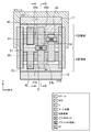
- FIG. 11 is an example of the layout of the circuit block included in the semiconductor integrated circuit apparatus according to the second embodiment.
- 12 (a) is a cross-sectional view taken along the line AA'of FIG. 11
- FIG. 12 (b) is a cross-sectional view taken along the line BB'of FIG.
- a plurality of cell row CRs including standard cells C arranged in the X direction are arranged side by side in the Y direction.
- the standard cell C includes, for example, a nanosheet FET.
- the plurality of cell rows CR are arranged upside down (inverted in the Y direction) every other row.
- the power supply wiring 3 for supplying the power supply voltage VDD and the power supply wiring 4 for supplying the power supply voltage VSS are alternately arranged between the cell rows CR.
- the power supply wirings 3 and 4 are so-called embedded power supply wirings (BPR) formed in the embedded wiring layer.
- Cell C included in each cell row CR is supplied with VDD and VSS from power supply wirings 3 and 4 arranged above and below the cell C.
- power tap cell groups 2a, 2b, 2c including a plurality of power tap cells 1 are arranged at equal intervals in the X direction.
- the power tap cell groups 2a, 2b, and 2c each include a plurality of power tap cells 1 located at the same position in the X direction.
- a local wiring extending in the Y direction is formed in the power tap cell 1.
- the power tap cells 1 are continuously arranged adjacent to each other in the Y direction, so that local power supply wirings 5 and 6 extending in the Y direction are formed in the circuit block.
- the local power supply wiring 5 is connected to the power supply wiring 3 for supplying VDD in the power supply tap cell 1 via vias.
- the local power supply wiring 6 is connected to the power supply wiring 4 for supplying VSS in the power supply tap cell 1 via vias.
- the configuration up to this point is the same as the layout of FIG. 1 in the first embodiment.
- metal power supply wirings 107 and 108 extending in the Y direction are formed in the M3 wiring layer (the third metal wiring layer from the bottom).
- the metal power supply wiring 107 is connected to the local power supply wiring 5 via M1 to M2 wirings and vias.
- the metal power supply wiring 108 is connected to the local power supply wiring 6 via M1 to M2 wirings and vias. That is, VDD is supplied from the metal power supply wiring 107 to the power supply wiring 3 via the local power supply wiring 5.
- VSS is supplied from the metal power supply wiring 108 to the power supply wiring 4 via the local power supply wiring 6.
- connection portion the configuration including the M1 to M2 wiring and vias that connect the metal power supply wiring and the local power supply wiring.
- the portion where the connecting portion is provided is indicated by the broken line A1.
- the connection portions 111 and 112 for connecting the metal power supply wiring 107 for supplying VDD and the local power supply wiring 5 are provided at predetermined intervals in the Y direction.
- the distance between the connection portions 111 and 112 is larger than the distance between the power supply wiring 3 that supplies VDD.
- connection portions 121 and 122 for connecting the metal power supply wiring 108 for supplying VSS and the local power supply wiring 6 are provided at predetermined intervals in the Y direction.
- the distance between the connection portions 121 and 122 is larger than the distance between the power supply wiring 4 that supplies VSS.
- connection portions 111 and 112 for connecting the metal power supply wiring 107 for supplying VDD and the local power supply wiring 5 and the connection portions 121 and 122 for connecting the metal power supply wiring 108 for supplying VSS and the local power supply wiring 6 are , The positions in the Y direction are aligned.
- power can be supplied from the upper metal power supply wirings 107 and 108 to the power supply wirings 3 and 4, which are embedded power supply wirings, via the local power supply wirings 5 and 6 extending in the Y direction, respectively. Therefore, in the M1 wiring layer and the metal wiring layer above it, it is not necessary to provide the metal power supply wiring corresponding to the embedded power supply wirings 3 and 4, respectively. Therefore, more metal wiring can be used as signal wiring in the M1 wiring layer and the metal wiring layer above it. Therefore, the area of the semiconductor integrated circuit device can be reduced.
- the power tap cell groups 2a, 2b, and 2c are arranged at equal intervals in the X direction, the power supply from the upper layer power supply wiring to the power supply wirings 3 and 4 can be made uniform in the circuit block. As a result, the power supply voltage drop can be effectively suppressed.
- connection portions 111 and 112 related to VDD and the connection portions 121 and 122 related to VSS are aligned in the Y direction. Therefore, the range in which the signal wiring cannot be laid is reduced due to the presence of the connection portion in the Y direction, and a larger area in which the signal wiring is laid can be secured. Therefore, the area of the semiconductor integrated circuit device can be reduced.
- connection part related to VDD and the connection part related to VSS do not have to be aligned in the Y direction.
- the metal power supply wirings 107 and 108 extending in the Y direction are formed in the M3 wiring layer, but the upper metal power supply wiring extending in the Y direction is formed in a wiring layer other than the M3 wiring layer. It may be formed. Further, the metal power supply wirings 107 and 108 are connected to the local power supply wirings 5 and 6 via the M1 to M2 wirings and vias, but instead of this, for example, the M3 wiring and the local wiring are directly connected. You may use the contact (super via) to be used.
- the power supply wiring may be further provided in the wiring layer above the M3 wiring layer. By connecting this power supply wiring to the metal power supply wirings 107 and 108 formed in the M3 wiring layer, the power supply can be strengthened.
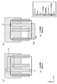
- FIG. 14A is a cross-sectional view taken along the line AA'of FIG. 13, and FIG. 14B is FIG. It is sectional drawing in line BB'.
- a plurality of cell row CRs including standard cells C arranged in the X direction are arranged side by side in the Y direction.
- the standard cell C includes, for example, a nanosheet FET.
- the plurality of cell rows CR are arranged upside down (inverted in the Y direction) every other row.
- a terminal cell row TCR1 in which the terminal cells TC1 are arranged side by side in the X direction is arranged at the upper end of the drawing of the circuit block, and a terminal cell TC2 arranged in the X direction is arranged at the lower end of the drawing of the circuit block.
- Column TCR2 is arranged.
- the terminal cells TC1 and TC2 have a uniform size, that is, a cell width in the X direction.
- the power supply wiring 203 for supplying the power supply voltage VDD and the power supply wiring 204 for supplying the power supply voltage VSS are alternately arranged. Unlike the first and second embodiments described above, the power supply wirings 203 and 204 are formed in the M1 wiring layer. Cell C included in each cell row CR is supplied with VDD and VSS from power supply wirings 203 and 204 arranged on both sides in the Y direction.
- power tap cell groups 202a, 202b, 202c including a plurality of power tap cells 201 are arranged at equal intervals in the X direction.
- the power tap cell groups 202a, 202b, and 202c each include a plurality of power tap cells 201 located at the same position in the X direction.
- Embedded wiring and local wiring extending in the Y direction are formed in the power tap cell 201.
- the power tap cells 201 are continuously arranged adjacent to each other in the Y direction, so that the embedded power wiring 205, 206 extending in the Y direction in the circuit block and Y in the circuit block.
- Local power supply wirings 5 and 6 extending in the direction are formed.
- the embedded power supply wiring 205 and the local power supply wiring 5 are connected to the power supply wiring 203 that supplies VDD in the power supply tap cell 201 via vias.
- the embedded power supply wiring 206 and the local power supply wiring 6 are connected to the power supply wiring 204 for supplying VSS in the power supply tap cell 201 via vias.
- Metal power supply wiring 107, 108 extending in the Y direction is formed in the M3 wiring layer (the third metal wiring layer from the bottom).
- the metal power supply wiring 107 is connected to the local power supply wiring 5 and the embedded power supply wiring 205 via the M1 to M2 wirings and vias in the power supply tap cells 201 arranged in the terminal cell rows TCR1 and TCR2.
- the metal power supply wiring 108 is connected to the local power supply wiring 6 and the embedded power supply wiring 206 via M1 to M2 wirings and vias in the power supply tap cells 201 arranged in the terminal cell rows TCR1 and TCR2. That is, VDD is supplied from the metal power supply wiring 107 to the power supply wiring 203 via the local power supply wiring 5 and the embedded power supply wiring 205.
- VSS is supplied from the metal power supply wiring 108 to the power supply wiring 204 via the local power supply wiring 6 and the embedded power supply wiring 206.
- FIG. 13 the locations where the metal power supply wiring 107, the local power supply wiring 5, and the embedded power supply wiring 205 are connected, and the locations where the metal power supply wiring 108, the local power supply wiring 6, and the embedded power supply wiring 206 are connected are shown by broken lines. It is shown by A2.
- FIG. 15 is a diagram showing an example of the layout structure of the power tap cell 201, (a) is a plan view, and (b) is a cross section of lines AA'.
- M1 wirings 251,252 extending in the X direction are provided, respectively.
- the M1 wiring 251 supplies the power supply voltage VDD
- the M1 wiring 252 supplies the power supply voltage VSS.
- the M1 wiring 251 is shared with other cells C arranged in the same cell row CR as the power tap cell 201, or with terminal cells TC1 and TC2 arranged in the same terminal cell rows TCR1 and TCR2 as the power tap cell 201.
- the power supply wiring 203 of FIG. 13 is formed.
- the M1 wiring 252 is shared with other cells C arranged in the same cell row CR as the power tap cell 201, or with terminal cells TC1 and TC2 arranged in the same terminal cell rows TCR1 and TCR2 as the power tap cell 201. ,
- the power supply wiring 204 of FIG. 13 is formed.
- the gate wiring 231 extends in the Y direction.
- Local wirings 241,242 extending in the Y direction are formed on both sides of the gate wiring 231 in the X direction.
- the local wirings 241,242 extend to the cell frame CL in the Y direction.
- embedded power supply wirings 211 and 212 extending in the Y direction so as to overlap with the local wirings 241,242 in a plan view are formed.
- the embedded power supply wirings 211 and 212 extend to the cell frame CL in the Y direction.
- the local wiring 241 and the embedded power supply wiring 211 are connected via vias.
- the local wiring 242 and the embedded wiring 212 are connected via via vias.
- the local wiring 241 is connected to the M1 wiring 251 via a via.
- the local wiring 242 is connected to the M1 wiring 252 via a via.
- the power tap cells 201 shown in FIG. 15 are arranged side by side in a row in the Y direction as shown in FIG.
- the embedded power supply wirings 211 and 212 are continuous across the plurality of power supply tap cells 201 arranged in the Y direction, and the embedded power supply wirings 205 and 206 of FIG. 13 are formed.
- the local wirings 241, 242 are continuous over the plurality of power tap cells 201 arranged in the Y direction, and the local power wirings 5 and 6 of FIG. 13 are formed.
- the local wiring 241 is connected to the M1 wiring 251 via a via
- the local wiring 242 is connected to the M1 wiring 252 via a via. It is connected and the local power supply wiring 6 is connected to the power supply wiring 204.
- the local power supply wirings 5 and 6 extending in the Y direction are connected to the metal power supply wirings 203 and 204 extending in the X direction, respectively.
- the embedded power supply wirings 205 and 206 extending in the Y direction overlap the local power supply wirings 5 and 6 in a plan view, and are connected to the local power supply wirings 5 and 6, respectively.
- Upper metal power supply wirings 107 and 108 extending in the Y direction are formed in the metal wiring layer above the metal power supply wirings 203 and 204, and the upper metal power supply wirings 107 and 108 are the local power supply wirings 5 and 6, respectively. It is connected.
- the power supply can be strengthened by the local power supply wirings 5 and 6 and the embedded power supply wirings 205 and 206 connected to each other. Further, since the upper metal power supply wirings 107 and 108 are connected to the local power supply wirings 5 and 6 only in the cell rows at both ends in the Y direction, it is necessary to secure a larger area for laying the signal wiring in the metal wiring layer. Can be done. Therefore, the area of the semiconductor integrated circuit can be reduced.
- logical cells may be arranged in the terminal cell columns TCR1 and TCR2.
- the metal power supply wirings 107 and 108 extending in the Y direction are formed in the M3 wiring layer, but the upper metal power supply wiring extending in the Y direction is formed in a wiring layer other than the M3 wiring layer. It may be formed. Further, the metal power supply wirings 107 and 108 are connected to the local power supply wirings 5 and 6 via the M1 to M2 wirings and vias, but instead of this, for example, the M3 wiring and the local wiring are directly connected. You may use the contact (super via) to be used.
- the power supply wiring may be further provided in the wiring layer above the M3 wiring layer. By connecting this power supply wiring to the metal power supply wirings 107 and 108 formed in the M3 wiring layer, the power supply can be strengthened.
- the power tap cells may not be arranged at equal intervals in the X direction.
- the power tap cells may be arranged at a narrower interval than other areas in the area where the power supply is desired to be further strengthened. That is, the power tap cells may be arranged at predetermined intervals in the X direction.
- the transistor in the cell C is a nanosheet FET, but the present invention is not limited to this, and may be, for example, a fin transistor. Further, although the nanosheet FET in the cell C has two nanosheets, the number of nanosheets is not limited to two.
- the width of the power tap cell (size in the X direction) is not limited to that shown in each of the above-described embodiments.
- the width of the power tap cell may be further increased, and two local wirings for supplying VDD and two local wirings for supplying VSS may be arranged.
- the width of the power tap cell may be reduced by using one local wiring, or the width of the power tap cell may be increased by arranging three or more local wirings in parallel. ..
Landscapes
- Design And Manufacture Of Integrated Circuits (AREA)
- Semiconductor Integrated Circuits (AREA)
Priority Applications (3)
| Application Number | Priority Date | Filing Date | Title |
|---|---|---|---|
| JP2021552360A JP7610127B2 (ja) | 2019-10-18 | 2020-10-08 | 半導体集積回路装置 |
| CN202080070169.8A CN114503256B (zh) | 2019-10-18 | 2020-10-08 | 半导体集成电路装置 |
| US17/719,052 US12094882B2 (en) | 2019-10-18 | 2022-04-12 | Semiconductor integrated circuit device |
Applications Claiming Priority (2)
| Application Number | Priority Date | Filing Date | Title |
|---|---|---|---|
| JP2019-191372 | 2019-10-18 | ||
| JP2019191372 | 2019-10-18 |
Related Child Applications (1)
| Application Number | Title | Priority Date | Filing Date |
|---|---|---|---|
| US17/719,052 Continuation US12094882B2 (en) | 2019-10-18 | 2022-04-12 | Semiconductor integrated circuit device |
Publications (1)
| Publication Number | Publication Date |
|---|---|
| WO2021075353A1 true WO2021075353A1 (ja) | 2021-04-22 |
Family
ID=75538437
Family Applications (1)
| Application Number | Title | Priority Date | Filing Date |
|---|---|---|---|
| PCT/JP2020/038192 Ceased WO2021075353A1 (ja) | 2019-10-18 | 2020-10-08 | 半導体集積回路装置 |
Country Status (4)
| Country | Link |
|---|---|
| US (1) | US12094882B2 (https=) |
| JP (1) | JP7610127B2 (https=) |
| CN (1) | CN114503256B (https=) |
| WO (1) | WO2021075353A1 (https=) |
Cited By (8)
| Publication number | Priority date | Publication date | Assignee | Title |
|---|---|---|---|---|
| JP2022553678A (ja) * | 2019-10-21 | 2022-12-26 | 東京エレクトロン株式会社 | 埋設電源レールを有するcfetのための電力供給ネットワーク |
| WO2023053203A1 (ja) * | 2021-09-28 | 2023-04-06 | 株式会社ソシオネクスト | 半導体集積回路装置 |
| JP2023097349A (ja) * | 2021-12-27 | 2023-07-07 | インターナショナル・ビジネス・マシーンズ・コーポレーション | デバイスおよび半導体デバイスを製造するための方法(密度スケーリングのための背面電源レールおよび配電網) |
| WO2023223501A1 (ja) * | 2022-05-19 | 2023-11-23 | 株式会社ソシオネクスト | 半導体装置 |
| WO2024210011A1 (ja) * | 2023-04-05 | 2024-10-10 | 株式会社ソシオネクスト | 出力回路 |
| WO2024214653A1 (ja) * | 2023-04-13 | 2024-10-17 | 株式会社ソシオネクスト | 半導体集積回路装置 |
| WO2024252661A1 (ja) * | 2023-06-09 | 2024-12-12 | 株式会社ソシオネクスト | 半導体装置 |
| US12317582B2 (en) | 2021-09-22 | 2025-05-27 | Samsung Electronics Co., Ltd. | Integrated circuit devices including a metal resistor and methods of forming the same |
Families Citing this family (1)
| Publication number | Priority date | Publication date | Assignee | Title |
|---|---|---|---|---|
| JP7640861B2 (ja) * | 2019-10-18 | 2025-03-06 | 株式会社ソシオネクスト | 半導体集積回路装置 |
Citations (3)
| Publication number | Priority date | Publication date | Assignee | Title |
|---|---|---|---|---|
| US20180151494A1 (en) * | 2016-11-28 | 2018-05-31 | Taiwan Semiconductor Manufacturing Co., Ltd. | Semiconductor device having buried metal line and fabrication method of the same |
| US20190080969A1 (en) * | 2017-09-12 | 2019-03-14 | Mediatek Inc. | Semiconductor structure with buried power rail, integrated circuit and method for manufacturing the semiconductor structure |
| US20190288004A1 (en) * | 2018-03-19 | 2019-09-19 | Tokyo Electron Limited | Three-dimensional device and method of forming the same |
Family Cites Families (2)
| Publication number | Priority date | Publication date | Assignee | Title |
|---|---|---|---|---|
| JP3810246B2 (ja) * | 2000-03-15 | 2006-08-16 | 株式会社ルネサステクノロジ | 半導体装置および半導体装置の製造方法 |
| WO2017145906A1 (ja) * | 2016-02-25 | 2017-08-31 | 株式会社ソシオネクスト | 半導体集積回路装置 |
-
2020
- 2020-10-08 WO PCT/JP2020/038192 patent/WO2021075353A1/ja not_active Ceased
- 2020-10-08 JP JP2021552360A patent/JP7610127B2/ja active Active
- 2020-10-08 CN CN202080070169.8A patent/CN114503256B/zh active Active
-
2022
- 2022-04-12 US US17/719,052 patent/US12094882B2/en active Active
Patent Citations (3)
| Publication number | Priority date | Publication date | Assignee | Title |
|---|---|---|---|---|
| US20180151494A1 (en) * | 2016-11-28 | 2018-05-31 | Taiwan Semiconductor Manufacturing Co., Ltd. | Semiconductor device having buried metal line and fabrication method of the same |
| US20190080969A1 (en) * | 2017-09-12 | 2019-03-14 | Mediatek Inc. | Semiconductor structure with buried power rail, integrated circuit and method for manufacturing the semiconductor structure |
| US20190288004A1 (en) * | 2018-03-19 | 2019-09-19 | Tokyo Electron Limited | Three-dimensional device and method of forming the same |
Cited By (10)
| Publication number | Priority date | Publication date | Assignee | Title |
|---|---|---|---|---|
| JP2022553678A (ja) * | 2019-10-21 | 2022-12-26 | 東京エレクトロン株式会社 | 埋設電源レールを有するcfetのための電力供給ネットワーク |
| JP7808747B2 (ja) | 2019-10-21 | 2026-01-30 | 東京エレクトロン株式会社 | 埋設電源レールを有するcfetのための電力供給ネットワーク |
| US12317582B2 (en) | 2021-09-22 | 2025-05-27 | Samsung Electronics Co., Ltd. | Integrated circuit devices including a metal resistor and methods of forming the same |
| WO2023053203A1 (ja) * | 2021-09-28 | 2023-04-06 | 株式会社ソシオネクスト | 半導体集積回路装置 |
| JPWO2023053203A1 (https=) * | 2021-09-28 | 2023-04-06 | ||
| JP2023097349A (ja) * | 2021-12-27 | 2023-07-07 | インターナショナル・ビジネス・マシーンズ・コーポレーション | デバイスおよび半導体デバイスを製造するための方法(密度スケーリングのための背面電源レールおよび配電網) |
| WO2023223501A1 (ja) * | 2022-05-19 | 2023-11-23 | 株式会社ソシオネクスト | 半導体装置 |
| WO2024210011A1 (ja) * | 2023-04-05 | 2024-10-10 | 株式会社ソシオネクスト | 出力回路 |
| WO2024214653A1 (ja) * | 2023-04-13 | 2024-10-17 | 株式会社ソシオネクスト | 半導体集積回路装置 |
| WO2024252661A1 (ja) * | 2023-06-09 | 2024-12-12 | 株式会社ソシオネクスト | 半導体装置 |
Also Published As
| Publication number | Publication date |
|---|---|
| US12094882B2 (en) | 2024-09-17 |
| US20220336499A1 (en) | 2022-10-20 |
| JP7610127B2 (ja) | 2025-01-08 |
| CN114503256B (zh) | 2024-09-06 |
| CN114503256A (zh) | 2022-05-13 |
| JPWO2021075353A1 (https=) | 2021-04-22 |
Similar Documents
| Publication | Publication Date | Title |
|---|---|---|
| WO2021075353A1 (ja) | 半導体集積回路装置 | |
| JP7799195B2 (ja) | 半導体集積回路装置 | |
| JP2021061278A (ja) | 半導体集積回路装置 | |
| JP7160105B2 (ja) | 半導体装置 | |
| KR100375753B1 (ko) | 반도체 소자의 파워/그라운드 금속 경로 설정 | |
| JP4781040B2 (ja) | 半導体集積回路装置 | |
| US20210305278A1 (en) | Semiconductor integrated circuit device | |
| US10157922B2 (en) | Interconnect metal layout for integrated circuit | |
| US20210320065A1 (en) | Semiconductor integrated circuit device | |
| US20220216319A1 (en) | Semiconductor integrated circuit device | |
| TWI502702B (zh) | 半導體裝置 | |
| JP2011233869A (ja) | 半導体装置、半導体装置のレイアウト装置、及び半導体装置のレイアウト方法 | |
| US20250113594A1 (en) | Semiconductor integrated circuit device | |
| EP3065171A2 (en) | Electronic device and electronic package thereof | |
| US20250329640A1 (en) | Semiconductor integrated circuit device | |
| CN111033720B (zh) | 半导体集成电路装置 | |
| JP2011199034A (ja) | 半導体装置 | |
| US8994098B2 (en) | Semiconductor device including pillar transistors | |
| TWI864518B (zh) | 半導體結構 | |
| WO2023132264A1 (ja) | 半導体集積回路装置 | |
| US7797660B2 (en) | Semiconductor integrated circuit for controlling substrate bias | |
| TWI880594B (zh) | 半導體裝置、積體電路裝置及其製造方法 | |
| WO2024214205A1 (ja) | 半導体装置 | |
| WO2025169463A1 (ja) | 半導体装置 | |
| WO2025079232A1 (ja) | 半導体装置 |
Legal Events
| Date | Code | Title | Description |
|---|---|---|---|
| 121 | Ep: the epo has been informed by wipo that ep was designated in this application |
Ref document number: 20876391 Country of ref document: EP Kind code of ref document: A1 |
|
| ENP | Entry into the national phase |
Ref document number: 2021552360 Country of ref document: JP Kind code of ref document: A |
|
| NENP | Non-entry into the national phase |
Ref country code: DE |
|
| 122 | Ep: pct application non-entry in european phase |
Ref document number: 20876391 Country of ref document: EP Kind code of ref document: A1 |