WO2021070366A1 - 半導体装置 - Google Patents
半導体装置 Download PDFInfo
- Publication number
- WO2021070366A1 WO2021070366A1 PCT/JP2019/040258 JP2019040258W WO2021070366A1 WO 2021070366 A1 WO2021070366 A1 WO 2021070366A1 JP 2019040258 W JP2019040258 W JP 2019040258W WO 2021070366 A1 WO2021070366 A1 WO 2021070366A1
- Authority
- WO
- WIPO (PCT)
- Prior art keywords
- power supply
- supply line
- region
- power
- semiconductor device
- Prior art date
- Legal status (The legal status is an assumption and is not a legal conclusion. Google has not performed a legal analysis and makes no representation as to the accuracy of the status listed.)
- Ceased
Links
Images











Classifications
-
- H—ELECTRICITY
- H10—SEMICONDUCTOR DEVICES; ELECTRIC SOLID-STATE DEVICES NOT OTHERWISE PROVIDED FOR
- H10W—GENERIC PACKAGES, INTERCONNECTIONS, CONNECTORS OR OTHER CONSTRUCTIONAL DETAILS OF DEVICES COVERED BY CLASS H10
- H10W20/00—Interconnections in chips, wafers or substrates
- H10W20/40—Interconnections external to wafers or substrates, e.g. back-end-of-line [BEOL] metallisations or vias connecting to gate electrodes
- H10W20/41—Interconnections external to wafers or substrates, e.g. back-end-of-line [BEOL] metallisations or vias connecting to gate electrodes characterised by their conductive parts
- H10W20/427—Power or ground buses
-
- H—ELECTRICITY
- H10—SEMICONDUCTOR DEVICES; ELECTRIC SOLID-STATE DEVICES NOT OTHERWISE PROVIDED FOR
- H10W—GENERIC PACKAGES, INTERCONNECTIONS, CONNECTORS OR OTHER CONSTRUCTIONAL DETAILS OF DEVICES COVERED BY CLASS H10
- H10W20/00—Interconnections in chips, wafers or substrates
- H10W20/40—Interconnections external to wafers or substrates, e.g. back-end-of-line [BEOL] metallisations or vias connecting to gate electrodes
- H10W20/41—Interconnections external to wafers or substrates, e.g. back-end-of-line [BEOL] metallisations or vias connecting to gate electrodes characterised by their conductive parts
- H10W20/43—Layouts of interconnections
-
- H—ELECTRICITY
- H10—SEMICONDUCTOR DEVICES; ELECTRIC SOLID-STATE DEVICES NOT OTHERWISE PROVIDED FOR
- H10D—INORGANIC ELECTRIC SEMICONDUCTOR DEVICES
- H10D89/00—Aspects of integrated devices not covered by groups H10D84/00 - H10D88/00
- H10D89/10—Integrated device layouts
-
- H—ELECTRICITY
- H10—SEMICONDUCTOR DEVICES; ELECTRIC SOLID-STATE DEVICES NOT OTHERWISE PROVIDED FOR
- H10W—GENERIC PACKAGES, INTERCONNECTIONS, CONNECTORS OR OTHER CONSTRUCTIONAL DETAILS OF DEVICES COVERED BY CLASS H10
- H10W20/00—Interconnections in chips, wafers or substrates
- H10W20/20—Interconnections within wafers or substrates, e.g. through-silicon vias [TSV]
-
- H—ELECTRICITY
- H10—SEMICONDUCTOR DEVICES; ELECTRIC SOLID-STATE DEVICES NOT OTHERWISE PROVIDED FOR
- H10W—GENERIC PACKAGES, INTERCONNECTIONS, CONNECTORS OR OTHER CONSTRUCTIONAL DETAILS OF DEVICES COVERED BY CLASS H10
- H10W20/00—Interconnections in chips, wafers or substrates
- H10W20/40—Interconnections external to wafers or substrates, e.g. back-end-of-line [BEOL] metallisations or vias connecting to gate electrodes
- H10W20/41—Interconnections external to wafers or substrates, e.g. back-end-of-line [BEOL] metallisations or vias connecting to gate electrodes characterised by their conductive parts
- H10W20/42—Vias, e.g. via plugs
-
- H—ELECTRICITY
- H10—SEMICONDUCTOR DEVICES; ELECTRIC SOLID-STATE DEVICES NOT OTHERWISE PROVIDED FOR
- H10W—GENERIC PACKAGES, INTERCONNECTIONS, CONNECTORS OR OTHER CONSTRUCTIONAL DETAILS OF DEVICES COVERED BY CLASS H10
- H10W20/00—Interconnections in chips, wafers or substrates
- H10W20/40—Interconnections external to wafers or substrates, e.g. back-end-of-line [BEOL] metallisations or vias connecting to gate electrodes
- H10W20/481—Interconnections external to wafers or substrates, e.g. back-end-of-line [BEOL] metallisations or vias connecting to gate electrodes on the rear surfaces of the wafers or substrates
-
- H—ELECTRICITY
- H10—SEMICONDUCTOR DEVICES; ELECTRIC SOLID-STATE DEVICES NOT OTHERWISE PROVIDED FOR
- H10D—INORGANIC ELECTRIC SEMICONDUCTOR DEVICES
- H10D84/00—Integrated devices formed in or on semiconductor substrates that comprise only semiconducting layers, e.g. on Si wafers or on GaAs-on-Si wafers
- H10D84/80—Integrated devices formed in or on semiconductor substrates that comprise only semiconducting layers, e.g. on Si wafers or on GaAs-on-Si wafers characterised by the integration of at least one component covered by groups H10D12/00 or H10D30/00, e.g. integration of IGFETs
- H10D84/82—Integrated devices formed in or on semiconductor substrates that comprise only semiconducting layers, e.g. on Si wafers or on GaAs-on-Si wafers characterised by the integration of at least one component covered by groups H10D12/00 or H10D30/00, e.g. integration of IGFETs of only field-effect components
- H10D84/83—Integrated devices formed in or on semiconductor substrates that comprise only semiconducting layers, e.g. on Si wafers or on GaAs-on-Si wafers characterised by the integration of at least one component covered by groups H10D12/00 or H10D30/00, e.g. integration of IGFETs of only field-effect components of only insulated-gate FETs [IGFET]
- H10D84/85—Complementary IGFETs, e.g. CMOS
- H10D84/856—Complementary IGFETs, e.g. CMOS the complementary IGFETs having different architectures than each other, e.g. high-voltage and low-voltage CMOS
-
- H—ELECTRICITY
- H10—SEMICONDUCTOR DEVICES; ELECTRIC SOLID-STATE DEVICES NOT OTHERWISE PROVIDED FOR
- H10D—INORGANIC ELECTRIC SEMICONDUCTOR DEVICES
- H10D84/00—Integrated devices formed in or on semiconductor substrates that comprise only semiconducting layers, e.g. on Si wafers or on GaAs-on-Si wafers
- H10D84/90—Masterslice integrated circuits
- H10D84/903—Masterslice integrated circuits comprising field effect technology
- H10D84/907—CMOS gate arrays
- H10D84/968—Macro-architecture
- H10D84/974—Layout specifications, i.e. inner core regions
- H10D84/981—Power supply lines
Definitions
- the present invention relates to a semiconductor device.
- Semiconductor devices include various circuit areas, and there is a standard cell area as an example of the circuit area.
- the standard cell area includes various logic circuits and power switch circuits.
- the power switch circuit is provided between, for example, a power supply line having a potential of VDD supplied to a semiconductor device and a power supply line supplying a power supply of V VDD to a transistor of a logic circuit, and supplies the power supply potential of V VDD to the transistor. Switch on / off.
- the power supply is turned off when it is not necessary to operate the logic circuit, the leakage current generated in the transistors constituting the logic circuit is suppressed, and the power consumption can be reduced.
- a technique has been proposed in which a subordinate semiconductor chip including wiring is attached to the back side of the main semiconductor chip, and a power supply potential is supplied to a transistor of the main semiconductor chip via the wiring of the subordinate semiconductor chip.
- Such a technology is sometimes called BS-PDN (backside-power delivery network).
- An object of the present invention is to provide a semiconductor device to which a power switch circuit can be appropriately provided.
- the semiconductor device has a first chip having a substrate, a first wiring layer formed on the first surface of the substrate, and the opposite of the first surface of the substrate. It has a second wiring layer formed on the second surface on the side, and the second wiring layer has a first power supply line to which a first power supply potential is supplied and a second power supply. It has a second power supply line to which an electric potential is supplied, and a switch connected between the first power supply line and the second power supply line, and the first chip is grounded first.
- the switch has a fourth power supply line to which the first power supply potential is supplied, and a second region in which the first ground line and the fourth power supply line are arranged, and the switch is viewed in a plan view. Is arranged between the first region and the second region.
- a power switch circuit can be appropriately provided.
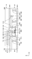
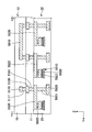
- FIG. 1 is a cross-sectional view showing an outline of the semiconductor device according to the first embodiment.
- FIG. 2 is a diagram showing the layout of the first chip in the first embodiment.
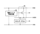
- FIG. 3 is a circuit diagram showing a configuration of a circuit included in the semiconductor device according to the first embodiment.
- FIG. 4 is a circuit diagram showing a buffer configuration.
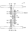
- FIG. 5 is a schematic view showing a planar configuration of the buffer.
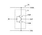
- FIG. 6 is a circuit diagram showing the configuration of the inverter.
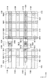
- FIG. 7 is a schematic view showing a planar configuration of the inverter.
- FIG. 8 is a schematic diagram showing an outline of the power domain in the first embodiment.
- FIG. 9 is a schematic view (No. 1) showing a planar configuration of the semiconductor device according to the first embodiment.
- FIG. 1 is a cross-sectional view showing an outline of the semiconductor device according to the first embodiment.
- FIG. 2 is a diagram showing the layout of the first chip in the first embodiment.
- FIG. 10 is a schematic view (No. 2) showing a planar configuration of the semiconductor device according to the first embodiment.
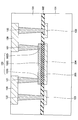
- FIG. 11 is a cross-sectional view (No. 1) showing the semiconductor device according to the first embodiment.
- FIG. 12 is a cross-sectional view (No. 2) showing the semiconductor device according to the first embodiment.
- FIG. 13 is a schematic view showing a planar configuration of the semiconductor device according to the second embodiment.
- FIG. 14 is a schematic view showing a planar configuration of the semiconductor device according to the third embodiment.
- FIG. 15 is a cross-sectional view showing the semiconductor device according to the third embodiment.
- FIG. 16 is a schematic view showing a planar configuration of the semiconductor device according to the fourth embodiment.
- FIG. 17 is a cross-sectional view showing the semiconductor device according to the fourth embodiment.
- FIG. 18 is a schematic view showing a planar configuration of the semiconductor device according to the fifth embodiment.
- FIG. 19 is a schematic view showing a planar configuration of the semiconductor device according to the sixth embodiment.
- FIG. 20 is a schematic diagram showing an outline of the power domain in the seventh embodiment.
- FIG. 21 is a schematic view showing a planar configuration of the semiconductor device according to the seventh embodiment.
- FIG. 22 is a schematic view showing a planar configuration of the semiconductor device according to the eighth embodiment.
- FIG. 23 is a cross-sectional view showing the semiconductor device according to the eighth embodiment.
- FIG. 24 is a schematic view showing an outline of the planar configuration of the semiconductor device according to the ninth embodiment.
- FIG. 25 is a cross-sectional view showing an outline of the semiconductor device according to the ninth embodiment.
- FIG. 26 is a schematic view showing a planar configuration of the semiconductor device according to the ninth embodiment.
- FIG. 27 is a cross-sectional view showing the configuration of the semiconductor device according to the ninth embodiment.
- FIG. 28 is a schematic view showing a planar configuration of the semiconductor device according to the tenth embodiment.
- FIG. 29 is a cross-sectional view showing the semiconductor device according to the eleventh embodiment.
- FIG. 30 is a cross-sectional view (No. 1) showing an example of the cross-sectional configuration of the switch transistor.
- FIG. 31 is a cross-sectional view (No. 2) showing an example of the cross-sectional configuration of the switch transistor.
- FIG. 1 is a cross-sectional view showing an outline of the semiconductor device according to the first embodiment.
- the semiconductor device according to the first embodiment includes a first chip 10 and a second chip 20.
- the first chip 10 is, for example, a semiconductor chip, and includes a substrate 11 and a first wiring layer 12.
- the substrate 11 is, for example, a silicon substrate, and a semiconductor element such as a transistor is formed on the surface side of the substrate 11.
- the transistor is, for example, a FinFET with fins 13 in the source, drain and channels.
- the first wiring layer 12 is formed on the surface of the substrate 11 and includes the wiring 14 and the insulating layer 15. A part of the wiring 14 is connected to the fin 13.
- a power supply line 16 connected to the wiring 14 is formed on the front surface side of the substrate 11, and the substrate 11 is provided with a via 17 extending from the power supply line 16 to the back surface of the substrate 11.
- the via 17 is, for example, a through-silicon via (TSV).
- TSV through-silicon via
- the second chip 20 is, for example, a semiconductor chip, and is arranged so as to face the back surface of the substrate 11 of the first chip 10.
- the second chip 20 includes, for example, a second wiring layer 22 and a pad 23.
- the second wiring layer 22 includes the wiring 24 and the insulating layer 25.
- the upper surface of the second wiring layer 22 faces, for example, the back surface of the substrate 11 of the first chip 10. That is, the substrate 11 is located between the first wiring layer 12 and the second wiring layer 22.
- the second wiring layer 22 may have a plurality of wirings 24.
- the plurality of wirings 24 may be connected via vias 28 provided in the second wiring layer 22.
- the pad 23 is an external connection terminal connected to, for example, a wiring board or a board. A part of the wiring 24 is connected to the via 17.
- the pad 23 is provided on the back surface of the second wiring layer 22, and is connected to the wiring 24 through the via 28.
- the power supply potential is supplied and the signal is transmitted to the second wiring layer 22 via the
- the second chip 20 may have a size similar to that of the first chip 10, or may have a size larger than that of the first chip 10. Further, the pad 23 may be provided on the surface of the second chip 20 on the side facing the first chip 10 and outside the first chip 10 in a plan view.
- the plan view means the plan view of the surface of the first chip 10.
- the second wiring layer 22 may be provided by forming the wiring 24, the insulating layer 25, and the like on the back surface of the substrate 11.
- the second wiring layer 22 may be formed on the second substrate on which the TSV is formed, or the pad 23 may be provided on the back surface of the second substrate.
- FIG. 1 shows an outline of the semiconductor device, and the details are shown in FIGS. 9 to 12.
- FIG. 2 is a diagram showing the layout of the first chip 10.
- the first chip 10 includes a first power domain 31A, a second power domain 31B, and an input / output (I / O) cell area 32.
- the I / O cell region 32 is arranged, for example, around the first power domain 31A and the second power domain 31B.
- the number of the first power domain 31A and the number of the second power domain 31B may be 2 or more.
- FIG. 3 is a circuit diagram showing a configuration of a circuit included in the semiconductor device according to the first embodiment.
- the semiconductor device includes a standard cell 41, a power switch circuit 42, and a power switch control circuit 52.
- the power switch control circuit 52 is provided in the first power domain 31A of the first chip 10.
- the standard cell 41 is provided in the second power domain 31B of the first chip 10.
- the standard cell 41 includes various logic circuits such as a NAND circuit and an inverter.
- the power switch control circuit 52 includes a buffer as described later.
- a VSS wiring that supplies the ground potential to the power switch control circuit 52 and a VDD wiring that supplies the power potential are arranged in the second power domain 31B.
- a VSS wiring for supplying the ground potential and a V VDD wiring for supplying the power supply potential are arranged in the standard cell 41.
- the power switch circuit 42 is provided on the second chip 20.
- the power switch circuit 42 includes a switch transistor 51.
- the switch transistor 51 is, for example, a P-channel MOS transistor, and is connected between the VDD wiring and the V VDD wiring.
- the power switch control circuit 52 is connected to the gate of the switch transistor 51 and controls the operation of the switch transistor 51.
- the power switch control circuit 52 switches the switch transistor 51 on / off, and controls the continuity between the VDD wiring and the V VDD wiring.
- the power switch control circuit 52 includes, for example, a buffer.
- the switch transistor 51 may be composed of a thin film transistor (TFT), or may be a microelectromechanical systems (MEMS) switch.
- TFT thin film transistor
- MEMS microelectromechanical systems
- VSS wiring that supplies the ground potential to the first power domain 31A and a VVSS wiring that supplies the ground potential to the second power domain 31B, and N as a switch transistor 51 between the VSS wiring and the VVSS wiring.
- a channel MOS transistor may be provided.
- FIG. 4 is a circuit diagram showing a buffer configuration.
- FIG. 5 is a schematic view showing a planar configuration of the buffer.
- the buffer 60 included in the power switch control circuit 52 includes an inverter 61 and an inverter 62.
- the input signal IN is input to the inverter 61
- the output of the inverter 61 is input to the gate of the switch transistor 51 and the inverter 62
- the output signal OUT is output from the inverter 62.
- the inverter 61 includes a P-channel MOS transistor 610P and an N-channel MOS transistor 610N.
- the inverter 62 includes a P-channel MOS transistor 620P and an N-channel MOS transistor 620N.
- a power supply line 1110 corresponding to VDD wiring and a power supply line 1120 corresponding to VSS wiring are provided.
- the power lines 1110 and 1120 extend in the X direction.
- a semiconductor fin 651 extending in the X direction is provided on the power supply line 1120 side of the power supply line 1110.
- a semiconductor fin 652 extending in the X direction is provided on the power supply line 1120 side of the fin 651.
- a local wiring 631 is provided which is connected to the power supply line 1110 via the via 681, extends in the Y direction, and is connected to the fin 651.
- a local wiring 632 that is connected to the power supply line 1120 via the via 682, extends in the Y direction, and is connected to the fin 652 is provided.
- Local wiring 634 connected to fins 651 and 652 is provided on the positive side in the X direction from the local wirings 631 and 632.
- Local wiring 636 connected to fins 651 and 652 is provided on the negative side in the X direction from the local wirings 631 and 632.
- a gate electrode 612 that intersects the fins 651 and 652 via a gate insulating film (not shown) is provided between the local wiring 631 and the local wiring 634, and between the local wiring 632 and the local wiring 634.
- a gate electrode 622 that intersects the fins 651 and 652 via a gate insulating film (not shown) is provided between the local wiring 631 and the local wiring 636, and between the local wiring 632 and the local wiring 636.
- the gate electrode 612 is connected to wiring 611 via local wiring 633 and via 641.
- the gate electrode 622 is connected to the control signal line 5110 via the local wiring 635 and via 643.
- the control signal line 5110 is also connected to the local wiring 634 via the via 642.
- the local wiring 636 is connected to the wiring 621 via the via 644.
- the input signal IN is input to the wiring 611, and the output signal OUT is output from the wiring 621 (see FIG. 4).
- the control signal line 5110 is connected to the gate of the switch transistor 51. That is, the control signal line 5110 functions as a signal line for transmitting a control signal to the switch transistor 51.
- the configurations of the inverters 61 and 62 are examples.
- the number of pairs of P-channel MOS transistors and N-channel MOS transistors included in the inverters 61 and 62 may be two or more.
- the wiring connected to the gate of the switch transistor 51 may be connected to the input or output of the buffer 60.
- FIG. 6 is a circuit diagram showing the configuration of the inverter.
- FIG. 7 is a schematic view showing a planar configuration of the inverter.
- the inverter 70 includes a P-channel MOS transistor 710P and an N-channel MOS transistor 710N.
- a power supply line 2110 corresponding to VSS wiring and a power supply line 2120 corresponding to VSS wiring are provided.
- the power lines 2110 and 2120 extend in the X direction.
- Semiconductor fins 751 extending in the X direction are provided on the power supply line 2120 side of the power supply line 2110.
- two fins 751 are provided.
- a semiconductor fin 752 extending in the X direction is provided on the power supply line 2120 side of the fin 751.
- a local wiring 731 that is connected to the power supply line 2110 via the via 781, extends in the Y direction, and is connected to the fin 751 is provided.
- a local wiring 732 connected to the power supply line 2120 via the via 782, extending in the Y direction, and connected to the fin 752 is provided.
- Local wiring 734 connected to fins 751 and 752 is provided on the positive side in the X direction from the local wirings 731 and 732.
- a gate electrode 712 that intersects the fins 751 and 752 via a gate insulating film (not shown) is provided between the local wiring 731 and the local wiring 734, and between the local wiring 732 and the local wiring 734.
- the gate electrode 712 is connected to the wiring 711 via the local wiring 733 and the via 741.
- the local wiring 734 is connected to the wiring 760 via the via 742.
- the input signal IN is input to the wiring 711, and the output signal OUT is output from the wiring 760 (see FIG. 6).
- the circuit included in the standard cell 41 is not limited to the inverter, and circuits such as various logic circuits may be included. Further, a memory cell of SRAM (Static Random Access Memory) may be included. Further, the circuit may be provided over the region where the power supply lines 2110 and 2120 are three or more. That is, a so-called multi-height circuit may be provided.
- SRAM Static Random Access Memory
- FIGS. 5 and 7 exemplify a transistor using fins (FinFET), a planar type transistor and a complementary field effect transistor (Complementary) are used in the first power domain 31A and the second power domain 31B.
- FieldEffectTransistor (CFET), a transistor using nanowires, and the like may be provided.
- FIG. 8 is a schematic diagram showing an outline of the power domain in the first embodiment.
- the second power domain 31B is located on the positive side of the first power domain 31A in the X direction.
- the first power domain 31A includes circuits connected to power lines 1110 and 1120.
- the buffer 60 of the power switch control circuit 52 shown in FIGS. 4 and 5 is included in the first power domain 31A.
- the second power domain 31B includes circuits connected to power lines 2110 and 2120.
- the inverter 70 shown in FIGS. 6 and 7 is included in the second power domain 31B.
- the power switch circuit 42 is located between the first power domain 31A and the second power domain 31B.
- the power line 1110 and the power line 2110 extend along the extending direction as shown in FIG. At least a part of the power domain 31A of 1 and the second power domain 31B may be arranged.
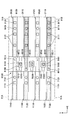
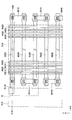
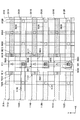
- FIGS. 9 and 10 are schematic views showing a planar configuration of the semiconductor device according to the first embodiment.
- 11 and 12 are cross-sectional views showing a semiconductor device according to the first embodiment.
- FIG. 9 shows the internal configuration of the first chip 10 and the second chip 20, and
- FIG. 10 shows the internal configuration of the second chip 20.
- FIG. 11 corresponds to a cross-sectional view taken along the line X11-X21 in FIGS. 9 and 10
- FIG. 12 corresponds to a cross-sectional view taken along the line X12-X22 in FIGS. 9 and 10.
- the power supply lines 1110 extending in the X direction and the power supply lines 1120 extending in the X direction are alternately arranged in the Y direction.
- the power supply line 1110 corresponds to the VDD wiring
- the power supply line 1120 corresponds to the VSS wiring.
- a plurality of grooves extending in the X direction are formed on the substrate 11, and the power supply lines 1110 and 1120 are formed in these grooves.
- the power supply lines 1110 and 1120 having such a structure are sometimes called BPR (Buried Power Rail).
- An element separation film (not shown) may be formed on the surface of the substrate 11.
- the element separation membrane is formed by, for example, the STI (Shallow Trench Isolation) method. The surface of the element separation membrane may or may not be flush with the surface of the substrate 11.
- Vias 1111 and 1121 that penetrate the substrate 11 to the back surface are formed on the substrate 11.
- the via 1111 is formed below the power line 1110 and the via 1121 is formed below the power line 1120.
- One power supply line 1110 may be provided with two or more vias 1111 or one power supply line 1120 may be provided with two or more vias 1121.
- a circuit such as the power switch control circuit 52 shown in FIG. 5 is connected between the power supply line 1110 and the power supply line 1120.
- the control signal line 5110 that transmits the output of the inverter 61 is located between the power supply line 1110 and the power supply line 1120 in a plan view.
- the control signal line 5110 extends to the region between the first power domain 31A and the second power domain 31B in plan view.
- a groove is formed in the substrate 11 below the end of the control signal line 5110 on the second power domain 31B side, and the connection layer 5190 is formed in the groove.
- the insulating layer 15 is formed with vias 5111 that electrically connect the control signal line 5110 and the connecting layer 5190.
- a via 5191 that penetrates the substrate 11 to the back surface is formed on the substrate 11.
- the via 5191 is formed below the connecting layer 5190.
- the power supply lines 2110 extending in the X direction and the power supply lines 2120 extending in the X direction are alternately arranged in the Y direction.
- the power supply line 2110 corresponds to the VSS wiring
- the power supply line 2120 corresponds to the VSS wiring.
- a plurality of grooves extending in the X direction are formed on the substrate 11, and the power supply lines 2110 and 2120 are formed in these grooves.
- Power lines 2110 and 2120 having such a structure may also be referred to as BPR.
- An element separation film (not shown) may be formed on the surface of the substrate 11.
- Vias 2111 and 2121 are formed on the substrate 11 so as to penetrate the substrate 11 to the back surface.
- the via 2111 is formed below the power supply line 2110 and the via 2121 is formed below the power supply line 2120.
- One power supply line 2110 may be provided with two or more vias 2111, or one power supply line 2120 may be provided with two or more vias 2121.
- the circuit included in the standard cell 41 such as the inverter 70 shown in FIG. 7 is connected between the power supply line 2110 and the power supply line 2120.
- a memory cell of the SRAM may be connected between the power supply line 2110 and the power supply line 2120.
- the second chip 20 includes, for example, an insulating layer 25 and power supply lines 7110, 7120, 8110, and 8120 formed on the surface layer portion of the insulating layer 25.
- the power lines 7110, 7120, 8110 and 8120 extend in the X direction.
- the power supply lines 7110 and 7120 are provided in an area overlapping the first power domain 31A in a plan view.
- the power supply line 7110 corresponds to the VDD wiring
- the power supply line 7120 corresponds to the VSS wiring.
- the power supply line 7110 overlaps with the power supply line 1110 and is connected to the power supply line 1110 via the via 1111.
- the power supply line 7120 overlaps the power supply line 1120 and is connected to the power supply line 1120 via the via 1121.
- a power supply line 7112 is provided below the power supply line 7110, and a via 7111 for connecting the power supply line 7112 and the power supply line 7110 is provided.
- a power supply line 7122 may be provided below the power supply line 7120, or a via 7121 connecting the power supply line 7122 and the power supply line 7120 may be provided.
- the power supply lines 7112 and 7122 may extend in the X direction or may extend in the Y direction.
- the power line 7122 and via 7121 may not be provided.
- the power supply lines 8110 and 8120 are provided in an area overlapping the second power domain 31B in a plan view.
- the power supply line 8110 corresponds to the VSS wiring
- the power supply line 8120 corresponds to the VSS wiring.
- the power supply line 8110 overlaps with the power supply line 2110 and is connected to the power supply line 2110 via the via 2111.
- the power supply line 8120 overlaps with the power supply line 2120 and is connected to the power supply line 2120 via via 2121.
- a power supply line 8112 may be provided below the power supply line 8110, or a via 8111 connecting the power supply line 8112 and the power supply line 8110 may be provided.
- FIG. 11 a power supply line 8112 may be provided below the power supply line 8110, or a via 8111 connecting the power supply line 8112 and the power supply line 8110 may be provided.
- a power supply line 8122 may be provided below the power supply line 8120, or a via 8121 connecting the power supply line 8122 and the power supply line 8120 may be provided.
- the power lines 8112 and 8122 may extend in the X direction or may extend in the Y direction.
- the second chip 20 includes a gate electrode 5120 in the insulating layer 25.
- the gate electrode 5120 is located below the power lines 7110, 7120, 8110 and 8120.
- the gate electrode 5120 is located between the first power domain 31A and the second power domain 31B.
- a connecting portion 5180 is formed on the surface layer portion of the insulating layer 25 above the gate electrode 5120.
- the connecting portion 5180 is connected to the via 5191.
- the insulating layer 25 is formed with vias 5181 that electrically connect the gate electrode 5120 and the connecting portion 5180.
- a plurality of semiconductor layers 6110 overlapping the power supply lines 7110 and 8110 are formed in the insulating layer 25 in a plan view.
- the semiconductor layer 6110 is located below the gate electrode 5120, and a gate insulating film 6120 is provided between the semiconductor layer 6110 and the gate electrode 5120.
- the gate insulating film 6120 is in contact with the gate electrode 5120, and the semiconductor layer 6110 is in contact with the gate insulating film 6120.
- the semiconductor layer 6110 has a V VDD connection portion 6111 (drain) and a VDD connection portion 6112 (source) with the center line of the semiconductor layer 6110 sandwiched in the X direction.
- the insulating layer 25 is formed with a via 8113 that electrically connects the V VDD connection portion 6111 and the power supply line 8110, and a via 7113 that electrically connects the VDD connection portion 6112 and the power supply line 7110.
- the plurality of semiconductor layers 6110 are arranged in the Y direction.
- the power supply line 7110 is connected to the VDD connection portion 6112 via the via 7113. Further, the V VDD connection unit 6111 is connected to the power supply line 2110 via the via 8113, the power supply line 8110, and the via 2111. The potential of VDD is supplied to the power supply line 7110 via, for example, the power supply line 7112 which is a part of the pad 23 (see FIG. 1). Further, as described above, the power supply line 2110 corresponds to the V VDD wiring.
- the conduction between the V VDD connection portion 6111 and the VDD connection portion 6112 is controlled by the potential of the gate electrode 5120. That is, the gate electrode 5120 functions as a gate of the switch transistor 51 connected between the VDD wiring and the V VDD wiring.
- the switch transistor 51 includes the semiconductor layer 6110, and the semiconductor layer 6110 is located between the first power domain 31A and the second power domain 31B in a plan view. That is, in a plan view, the switch transistor 51 is located between the first power domain 31A and the second power domain 31B.
- an area for power supply separation is provided between the first power domain 31A and the second power domain 31B. Therefore, according to the present embodiment, in the first chip 10, between the first power domain 31A and the second power domain 31B, in addition to the region for power supply separation (separation region), the switch transistor The size of the semiconductor device can be reduced as compared with the case where the 51 is arranged.
- connection layer 5190 having the same structure as the BPR can be used for connecting the control signal line 5110 and the connection portion 5180.
- the number of vias 2111 and 2121 is not limited. As the number of vias 2111 and 2121 increases, the resistance between the power supply line 2110 and the power supply line 8110 and the resistance between the power supply line 2120 and the power supply line 8120 can be lowered, and IR drop can be suppressed.
- the power supply lines 7112, 7122, 8112 and 8122 may extend in the Y direction.
- the power line 8112 may not be provided.
- each via is not particularly limited, and may be, for example, a circle, an ellipse, a square, a rectangle, or the like.
- FIG. 13 is a schematic view showing a planar configuration of the semiconductor device according to the second embodiment.
- a semiconductor layer 6210 is provided instead of the plurality of semiconductor layers 6110.
- the semiconductor layer 6210 overlaps with the power supply lines 7110 and 8110 in a plan view and extends in the Y direction.
- a gate electrode 5220 extending in the Y direction is provided above the semiconductor layer 6210.
- a gate insulating film (not shown) is provided between the gate electrode 5220 and the semiconductor layer 6210 in place of the gate insulating film 6120. The gate insulating film is in contact with the gate electrode 5220, and the semiconductor layer 6210 is in contact with the gate insulating film.
- the semiconductor layer 6210 has a V VDD connection portion 6211 and a VDD connection portion 6212 with the center line of the semiconductor layer 6210 interposed therebetween in the X direction.
- the insulating layer 25 is formed with a via 8113 that electrically connects the V VDD connection portion 6211 and the power supply line 8110, and a via 7113 that electrically connects the VDD connection portion 6212 and the power supply line 7110.
- a plurality of power supply lines 8110 are connected to one V VDD connection unit 6211 via a plurality of vias 8113
- a plurality of power supply lines 7110 are connected to one VDD connection unit 6212 via a plurality of vias 7113.
- the switch transistor 51 includes a semiconductor layer 6210, and the semiconductor layer 6210 is located between the first power domain 31A and the second power domain 31B in a plan view. That is, in a plan view, the switch transistor 51 is located between the first power domain 31A and the second power domain 31B.
- the size of the semiconductor device can be reduced as in the first embodiment. In addition, efficiency can be improved.
- FIG. 14 is a schematic view showing a planar configuration of the semiconductor device according to the third embodiment.
- FIG. 15 is a cross-sectional view showing the semiconductor device according to the third embodiment.
- FIG. 15 corresponds to a cross-sectional view taken along the line X13-X23 in FIG.
- a power supply line 7320 is provided in place of the power supply lines 7120 and 8120.
- the power supply line 7320 is provided on the surface layer portion of the insulating layer 25.
- the power line 7320 extends in the X direction.
- the power supply line 7320 is provided in a region overlapping the first power domain 31A, a region overlapping the second power domain 31B, and a region between them in a plan view.
- the power line 7320 corresponds to VSS wiring.
- the power supply line 7320 overlaps the power supply lines 1120 and 2120 in a plan view, and is connected to the power supply lines 1120 and 2120 via vias 1121 and 2121.
- a power supply line 7322 may be provided below the power supply line 7320 instead of the power supply lines 7122 and 8122, and the power supply line 7322 is connected to the power supply line 7320 via vias 7121 and 8121. You may be.
- the same effect as that of the first embodiment can be obtained by the third embodiment. Further, in the third embodiment, since the VSS wiring is shared between the first power domain 31A and the second power domain 31B, the power supply noise generated in the VDD wiring can be reduced.
- FIG. 16 is a schematic view showing a planar configuration of the semiconductor device according to the fourth embodiment.
- FIG. 17 is a cross-sectional view showing the semiconductor device according to the fourth embodiment.
- FIG. 17 corresponds to a cross-sectional view taken along the line X14-X24 in FIG.
- power supply lines 7410, 7420, 8410 and 8420 are provided in place of the power supply lines 7110, 7120, 8110 and 8120.
- the power supply lines 7410, 7420, 8410 and 8420 are provided on the surface layer portion of the insulating layer 25.
- the power lines 7410, 7420, 8410 and 8420 extend in the Y direction.
- the power supply lines 7410 and 7420 are provided in a region overlapping the first power domain 31A in a plan view.
- the power supply line 7410 corresponds to the VDD wiring
- the power supply line 7420 corresponds to the VSS wiring.
- the power supply line 7410 is orthogonal to the power supply lines 1110 and 1120 and is connected to the power supply line 1110 via vias 1111.
- the power supply line 7420 is orthogonal to the power supply lines 1110 and 1120 and is connected to the power supply line 1120 via the via 1121.
- a power supply line 7112 may be provided below the power supply line 1110, and a via 7421 connecting the power supply line 7112 and the power supply line 7420 may be provided.
- a power supply line (not shown) corresponding to VDD wiring is provided below the power supply line 1120, and as shown in FIG. 16, a via 7411 for connecting the power supply line and the power supply line 7410 is provided.
- the power lines 1110 and 7410 have a mesh structure in a plan view.
- the power lines 1120 and 7420 have a mesh structure in a plan view.
- the power supply lines 8410 and 8420 are provided in an area overlapping the second power domain 31B in a plan view.
- the power supply line 8410 corresponds to the VSS wiring
- the power supply line 8420 corresponds to the VSS wiring.
- the power supply line 8410 is orthogonal to the power supply lines 2110 and 2120 and is connected to the power supply line 2110 via vias 2111.
- the power supply line 8420 is orthogonal to the power supply lines 2110 and 2120 and is connected to the power supply line 2120 via via 2121.
- a power supply line 8112 may be provided below the power supply line 2110, and a via 8421 connecting the power supply line 8112 and the power supply line 8420 may be provided.
- a power supply line (not shown) corresponding to the V VDD wiring is provided below the power supply line 2120, and as shown in FIG. 16, a via 8411 for connecting the power supply line and the power supply line 8410 is provided.
- the power lines 2110 and 8410 have a mesh structure in a plan view.
- the power lines 2120 and 8420 have a mesh structure in a plan view.
- a plurality of power supply lines 1110 can be commonly connected to the VDD connection portion 6412 of each switch transistor 51, and a plurality of power supply lines 2110 can be commonly connected to the V VDD connection portion 6411 of each switch transistor 51. Further, the power supply can be redistributed via the power supply lines 7112, 8112 and the like.
- the number of power lines 7410, 7420, 8410 and 8420 is not limited.
- the width of the power supply line 7410 connected to the VDD connection portion 6412 via the via 7413 among the plurality of power supply lines 7410 may be larger than the width of the other power supply lines 7410. .
- the width of the power supply line 8410 connected to the V VDD connection portion 6411 via the via 8413 among the plurality of power supply lines 8410 may be larger than the width of the other power supply lines 8410. ..
- FIG. 18 is a schematic view showing a planar configuration of the semiconductor device according to the fifth embodiment. In FIG. 18, the portion corresponding to the control signal line 5110 is omitted.
- a semiconductor layer 6510 is provided in place of the plurality of semiconductor layers 6110, a power supply line 7510 is provided in place of the power supply line 7110, and a power supply line is provided in place of the power supply line 8110. 8510 is provided.
- the power supply line 7510 corresponds to the VDD wiring, and the power supply line 8510 corresponds to the V VDD wiring.
- the power supply line 7510 is provided in a region overlapping the first power domain 31A in a plan view.
- the power supply line 7510 further extends between the first power domain 31A and the second power domain 31B to the vicinity of the power supply line 8120.
- the power supply line 8510 is provided in a region overlapping the second power domain 31B in a plan view.
- the power supply line 8510 further extends between the first power domain 31A and the second power domain 31B to the vicinity of the power supply line 7120. Then, in the Y direction view, the power supply lines 7510 and 8510 overlap each other.
- the semiconductor layer 6510 overlaps with the power supply lines 7510 and 8510 in a plan view and extends in the Y direction. Further, instead of the gate electrode 5120, a gate electrode 5520 extending in the X direction is provided above the semiconductor layer 6510. The gate electrode 5520 is located between the end of the power supply line 7510 on the power supply line 8120 side and the end of the power supply line 8510 on the power supply line 7120 side, which are adjacent to each other in the Y direction.
- the semiconductor layer 6110 has a VDD connection portion 6512 around the end portion of the power supply line 7510 on the power supply line 8120 side in a plan view, and a V VDD connection portion around the end portion of the power supply line 8510 on the power supply line 7120 side in a plan view.
- a gate insulating film (not shown) is provided between the gate electrode 5520 and the semiconductor layer 6510 in place of the gate insulating film 6120.
- the gate insulating film is in contact with the gate electrode 5520, and the semiconductor layer 6510 is in contact with the gate insulating film.
- the insulating layer 25 is formed with vias 8513 that electrically connect the V VDD connection portion 6511 and the power supply line 8510, and vias 7513 that electrically connect the VDD connection portion 6512 and the power supply line 7510.
- FIG. 19 is a schematic view showing a planar configuration of the semiconductor device according to the sixth embodiment. In FIG. 19, the portion corresponding to the control signal line 5110 is omitted.
- a common connection portion 7610 is provided which is commonly connected to two power supply lines 7110 adjacent to each other with one power supply line 7120 sandwiched in the Y direction. ..
- the common connection portion 7610 is connected to the end of the power supply line 7110 on the second power domain 31B side, and extends to a region between the first power domain 31A and the second power domain 31B in a plan view.
- the end of the common connection portion 7610 on the second power domain 31B side is located in the vicinity of the second power domain 31B.
- the power supply line 7120 between the two power supply lines 7110 connected to the common connection portion 7610 is separated from the common connection portion 7610 in the X direction.
- a common connection portion 8610 is provided which is commonly connected to two adjacent power supply lines 8110 with one power supply line 8120 sandwiched in the Y direction.
- the common connection portion 8610 is connected to the end of the power supply line 8110 on the first power domain 31A side, and extends to a region between the first power domain 31A and the second power domain 31B in a plan view.
- the end of the common connection portion 8610 on the first power domain 31A side is located in the vicinity of the first power domain 31A.
- the power supply line 8120 between the two power supply lines 8110 connected to the common connection portion 8610 is separated from the common connection portion 8610 in the X direction.
- a semiconductor layer 6610 is provided in place of the semiconductor layer 6110. Each semiconductor layer 6610 is arranged so as to overlap a part of the common connection portion 8610 adjacent to each other in the Y direction and a part of the common connection portion 7610. Further, instead of the gate electrode 5120, a gate electrode 5620 extending in the X direction is provided above the semiconductor layer 6610. The gate electrode 5620 is located between the common connection portion 8610 and the common connection portion 7610, which are adjacent to each other in the Y direction.
- the semiconductor layer 6610 has a VDD connection portion 6612 around the common connection portion 7610 in a plan view, and has a V VDD connection portion 6611 around the common connection portion 8610 in a plan view.
- a gate insulating film (not shown) is provided between the gate electrode 5620 and the semiconductor layer 6610 in place of the gate insulating film 6120.
- the gate insulating film is in contact with the gate electrode 5620, and the semiconductor layer 6610 is in contact with the gate insulating film.
- the insulating layer 25 is formed with a via 8613 that electrically connects the V VDD connection portion 6611 and the common connection portion 8610, and a via 7613 that electrically connects the VDD connection portion 6612 and the common connection portion 7610. .
- each common connection portion 7610 is connected to the VDD connection portion 6612 of the two switch transistors 51, and each common connection portion 8610 is connected to the V VDD connection portion 6611 of the two switch transistors 51.
- FIG. 20 is a schematic diagram showing an outline of the power domain in the seventh embodiment.
- FIG. 21 is a schematic view showing a planar configuration of the semiconductor device according to the seventh embodiment.
- the third power domain 31C is provided on the negative side in the Y direction of the second power domain 31B.
- the third power domain 31C like the first power domain 31A, includes circuits connected to power lines 1110 and 1120.
- the power switch circuit 42 is provided between the third power domain 31C and the second power domain 31B.
- the second power domain 31B is arranged surrounded by the third power domain 31C, as shown in FIG. 20, in the direction orthogonal to the extending direction of the power supply line 1110 and the power supply line 2110. Along the line, at least a part of the third power domain 31C and the second power domain 31B may be arranged.
- power lines 2110, 2120, 8410, 8420 and the like are provided in the second power domain 31B. Further, the power supply lines 1110, 1120, 7410, 7420 and the like are provided in the third power domain 31C. Further, instead of the control signal line 5110, a control signal line 5710 extending in the Y direction is provided. The control signal line 5710 is connected to the connection layer 5190 via the via 5111 (see FIG. 11). The power supply lines 7410, 7420, 8410 and 8420 are provided on the surface layer portion of the insulating layer 25 and extend in the Y direction, as in the fourth embodiment.
- a semiconductor layer 6710 is provided between the second power domain 31B and the third power domain 31C.
- the semiconductor layer 6710 overlaps with the power supply lines 7410 and 8410 in a plan view and extends in the X direction.
- a gate electrode 5720 extending in the X direction is provided above the semiconductor layer 6710.
- a gate insulating film (not shown) is provided between the gate electrode 5720 and the semiconductor layer 6710. The gate insulating film is in contact with the gate electrode 5720, and the semiconductor layer 6710 is in contact with the gate insulating film.
- the semiconductor layer 6710 has a V VDD connection portion 6711 and a VDD connection portion 6712 with the center line of the semiconductor layer 6710 interposed therebetween in the Y direction.
- the insulating layer 25 is formed with vias 8713 that electrically connect the V VDD connection portion 6711 and the power supply line 8410, and vias 7713 that electrically connect the VDD connection portion 6712 and the power supply line 7410.
- a plurality of power supply lines 8410 are connected to one V VDD connection unit 6711 via a plurality of vias 8713
- a plurality of power supply lines 7410 are connected to one VDD connection unit 6712 via a plurality of vias 7713.
- the configuration of the switch transistor 51 provided in the seventh embodiment follows the configuration of the switch transistor 51 in the second embodiment.
- the configuration of the switch transistor 51 provided between the second power domain 31B and the third power domain 31C may be similar to the configuration of the switch transistor 51 in another embodiment.
- each power supply line does not have to be provided on the surface layer portion of the insulating layer 25, and may be provided inside the insulating layer 25. Further, the power supply line provided on the surface layer portion of the insulating layer 25 may extend in the X direction.
- a first power domain 31A may be provided in addition to the second power domain 31B and the third power domain 31C, between the first power domain 31A and the second power domain 31B, and the second.
- a power switch circuit 42 may be provided between the power domain 31B and the third power domain 31C.
- FIG. 22 is a schematic view showing a planar configuration of the semiconductor device according to the eighth embodiment.
- FIG. 23 is a cross-sectional view showing the semiconductor device according to the eighth embodiment.
- FIG. 23 corresponds to a cross-sectional view taken along the line X15-X25 in FIG.
- the semiconductor layer 6810 is provided in place of the semiconductor layer 6110.
- the semiconductor layer 6810 overlaps the power supply lines 7110 and 8110 in a plan view.
- a gate electrode 5820 is provided below the semiconductor layer 6210.
- a gate insulating film 6820 is provided between the gate electrode 5820 and the semiconductor layer 6810 instead of the gate insulating film 6120. The gate insulating film 6820 is in contact with the gate electrode 5820, and the semiconductor layer 6810 is in contact with the gate insulating film 6820.
- the gate electrode 5820 may be formed in the same layer as the power supply lines 7112 and 8112.
- the gate electrode 5820 may be formed of the same material as the power supply lines 7112 and 8112 and the like.
- the control signal line 5110 may extend in the Y direction and be connected to a plurality of gate electrodes 5820 via a plurality of vias 5111 and the like.
- the gate electrode and the gate insulating film may be located below the semiconductor layer.
- FIG. 24 is a schematic view showing an outline of the planar configuration of the semiconductor device according to the ninth embodiment.
- FIG. 25 is a cross-sectional view showing an outline of the semiconductor device according to the ninth embodiment.
- a part relating to the arrangement of control signal lines, which is a characteristic part of the ninth embodiment, is illustrated, and the semiconductor layer, some power lines, vias, and the like are not shown.
- a plurality of control signal lines 5930 are arranged in the insulating layer 25.
- the control signal lines 5930 extend in the X direction and are arranged side by side in the Y direction.
- Each control signal line 5930 has a portion protruding from both ends of the second power domain 31B in the X direction.
- the control signal lines 5930 adjacent to each other in the Y direction are connected to each other via the control signal lines 5910 extending in the Y direction outside the second power domain 31B.
- the control signal line 5930 connected to the control signal line 5930 located on the positive side in the Y direction via the control signal line 5910 on the negative side in the X direction is on the negative side in the Y direction via the control signal line 5910 on the positive side in the X direction. It is connected to the located control signal line 5930.
- the control signal line 5930 connected to the control signal line 5930 located on the positive side in the Y direction via the control signal line 5910 on the positive side in the X direction is connected to the control signal line 5930 on the negative side in the X direction via the control signal line 5910 in the Y direction. It is connected to the control signal line 5930 located on the negative side.
- the control signal lines 5930 adjacent to each other in the Y direction are connected to each other only outside the second power domain 31B.
- a gate electrode (not shown) of the switch transistor 51 is connected to the control signal line 5910. That is, a plurality of switch transistors 51 are connected in parallel.
- FIG. 26 is a schematic view showing a planar configuration of the semiconductor device according to the ninth embodiment.
- FIG. 27 is a cross-sectional view showing the configuration of the semiconductor device according to the ninth embodiment.
- FIG. 27 corresponds to a cross-sectional view taken along the line Y11-Y21 in FIG. 26.
- control signal line 5930 extends in the X direction below the semiconductor layer 6410.
- a connecting portion 5920 is provided at a portion of the surface layer portion of the insulating layer 25 that overlaps with the control signal line 5110 or 5910 in a plan view.
- a via 5921 is provided to electrically connect the control signal line 5930 and the connecting portion 5920.
- a via 5922 is provided below the connecting portion 5920 in addition to the via 5921.
- a gate electrode 5923 connected to the via 5922 is provided, and a gate insulating film 6920 and a semiconductor layer 6910 are provided under the gate electrode 5923.
- the semiconductor layer 6910 has a V VDD connection portion 6911 and a VDD connection portion 6912 with the center line of the semiconductor layer 6910 interposed therebetween in the X direction.
- the insulating layer 25 includes a via 8913 that electrically connects the V VDD connection portion 6911 and the power supply line 8110 (see FIGS. 9 to 12), and a VDD connection portion 6912 and the power supply line 7110 (see FIGS. 9 to 12).
- a via 7913 is formed to electrically connect the two.
- the plurality of semiconductor layers 6910 are arranged in the Y direction.
- the switch transistor 51 is provided in the region where the control signal line 5930 and the control signal line 5110 or 5910 intersect in a plan view.
- the capacitance and resistance parasitic on the control signal line 5930 are large. Then, the control signal from the power switch control circuit is sequentially transmitted to each switch transistor 51 through the control signal line 5930. Therefore, the rise of the V VDD potential in the second power domain 31B becomes gentle, and the power supply noise due to the steep rise of the potential can be reduced.
- control signal lines 5930 adjacent to each other in the Y direction are connected outside the second power domain 31B in a plan view via a control signal line provided on the surface layer of the second chip 20 instead of the control signal line 5910. It may have been done.
- FIG. 28 is a schematic view showing a planar configuration of the semiconductor device according to the tenth embodiment.
- a part relating to the arrangement of control signal lines, which is a characteristic part of the tenth embodiment, is shown, and the semiconductor layer, some power lines, vias, and the like are not shown.
- a buffer 5700 is added to the control signal lines 5110 and 5910.
- the buffer 5700 is provided on the first chip 10.
- the buffer 5700 is supplied with voltage from the VDD wiring and the VSS wiring in the same manner as the buffer 60.
- the buffer 5700 may be provided in the first power domain 31A in the same manner as the buffer 60.
- Other configurations are the same as in the ninth embodiment.
- the buffer 5700 can function as a delay circuit. Therefore, the operation timing of the switch transistor 51 can be controlled by using the delay in the transmission of the control signal by the buffer 5700.
- FIG. 29 is a cross-sectional view showing the semiconductor device according to the eleventh embodiment.
- a part relating to a control signal line and a switch transistor, which are characteristic parts of the eleventh embodiment, is illustrated, and the semiconductor layer, a part of the power supply line, vias, and the like are not shown.
- the wiring capacitance unit 5941 including the wiring 5931 and the wiring 5932 adjacent to each other is connected to the control signal line 5930 via the via 5951.
- the wires 5931 and 5932 extend in the Y direction, and the via 5951 is connected to the wire 5931.
- the wiring 5933 extending in the Y direction is connected to the control signal line 5930 via the via 5952.
- An insulating film 5934 and a conductive film 5935 are formed on the wiring 5933.
- the capacitive element 5942 is composed of the wiring 5933, the insulating film 5934, and the conductive film 5935.
- the wiring capacitance unit 5941 and the capacitance element 5942 parasitize the control signal line 5930 with a larger capacitance. Therefore, the effect of suppressing the steep rise of the potential can be made higher.
- the wiring capacitance section 5941 or the capacitance element 5942 may be provided. In other embodiments, the wiring capacitance section 5941 may be provided, the capacitance element 5942 may be provided, or both of them may be provided.
- 30 and 31 are cross-sectional views showing an example of the cross-sectional configuration of the switch transistor.
- the underlying insulating film 102 is provided in the insulating layer 101, and the semiconductor layer 103, the gate insulating film 104, and the gate electrode 105 are provided on the underlying insulating film 102.
- a control signal line 110, a power supply line 120 corresponding to VDD wiring, and a power supply line 130 corresponding to V VDD wiring are provided on the surface layer portion of the insulating layer 101.
- the semiconductor layer 103 has a channel 103C and a source 103S and a drain 103D sandwiching the channel 103C.
- the power supply line 120 and the source 103S are connected via the via 121, and the power supply line 130 and the drain 103D are connected via the via 131.
- a power supply line 123 corresponding to VDD wiring and a power supply line 133 corresponding to V VDD wiring are provided under the underlying insulating film 102.
- the power supply line 120 and the power supply line 123 are connected via the via 122, and the power supply line 130 and the power supply line 133 are connected via the via 132.
- the control signal line 110 is connected to the gate electrode 105 via the via 111.
- the gate insulating film 204 is provided in the underlying insulating film 102, the semiconductor layer 103 is provided on the gate insulating film 204, and the gate electrode 205 is provided under the gate insulating film 204.
- Other configurations are the same as in the first example.
- the material of the underlying insulating film is, for example, silicon oxide, silicon nitride, silicon carbide, silicon oxide nitride, silicon oxide carbide, or the like.
- the material of the semiconductor layer is, for example, InGaZnO (IGZO), ZnO, ZnSnO, InZnO, or the like.
- the material of the gate insulating film is, for example, SiO 2 , SiO x N y , SiN, Al 2 O 3, and the like.
- the material of the gate electrode is a metal such as molybdenum, titanium, chromium, tantalum, magnesium, silver, tungsten, aluminum, copper, neodymium, ruthenium, scandium and the like.
- the material of the gate electrode may be graphene or the like.
- the switch transistors 51 provided in each of the above embodiments can be classified into the first and second examples from the viewpoint of the stacking relationship between the gate electrode and the semiconductor layer and the connection relationship between the semiconductor layer and the VDD wiring as follows. Become. That is, the switch transistors 51 provided in the first to seventh, ninth, and tenth embodiments are classified into the first example. The switch transistor 51 provided in the eighth embodiment is classified into the second example.
- the present invention has been described above based on each embodiment, the present invention is not limited to the requirements shown in the above embodiments. With respect to these points, the gist of the present invention can be changed without impairing the gist of the present invention, and can be appropriately determined according to the application form thereof.
- First chip 20 Second chip 31A, 31B, 31C: Power domain 42: Power switch circuit 51: Switch transistor 52: Power switch control circuit
Landscapes
- Semiconductor Integrated Circuits (AREA)
- Design And Manufacture Of Integrated Circuits (AREA)
- Metal-Oxide And Bipolar Metal-Oxide Semiconductor Integrated Circuits (AREA)
- Physics & Mathematics (AREA)
- Geometry (AREA)
- Thin Film Transistor (AREA)
- Internal Circuitry In Semiconductor Integrated Circuit Devices (AREA)
Abstract
半導体装置は、基板と、前記基板の第1の面上に形成された第1の配線層と、を有する第1のチップと、前記基板の前記第1の面とは反対側の第2の面上に形成された第2の配線層と、を有する。前記第2の配線層は、第1の電源電位が供給される第1の電源線と、第2の電源電位が供給される第2の電源線と、前記第1の電源線と前記第2の電源線との間に接続されたスイッチと、を有する。前記第1のチップは、第1の接地線と、前記第2の電源電位が供給される第3の電源線と、前記第1の接地線及び前記第3の電源線が配置された第1の領域と、第2の接地線と、前記第1の電源電位が供給される第4の電源線と、前記第1の接地線及び前記第4の電源線が配置された第2の領域と、を有する。平面視で、前記スイッチは前記第1の領域と前記第2の領域との間に配置されている。
Description
本発明は、半導体装置に関する。
半導体装置には各種回路領域が含まれており、回路領域の一例としてスタンダードセル領域がある。スタンダードセル領域には各種論理回路及び電源スイッチ回路が含まれる。
電源スイッチ回路は、例えば半導体装置に供給されるVDDの電位の電源線と論理回路のトランジスタにVVDDの電源を供給する電源線との間に設けられ、当該トランジスタへのVVDDの電源電位の供給のオン/オフを切り替える。電源スイッチ回路を用いることで、論理回路を動作させる必要のないときに電源供給をオフとし、論理回路を構成するトランジスタで生じるリーク電流を抑制し、消費電力の低減が可能となる。
また、主たる半導体チップの裏側に、配線を含む従たる半導体チップを貼り付け、従たる半導体チップの配線を介して主たる半導体チップのトランジスタに電源電位を供給する技術が提案されている。このような技術はBS-PDN(backside-power delivery network)とよばれることがある。
これまでのところ、配線を含む従たる半導体チップ内に電源スイッチ回路を設ける場合の具体的な構成について、詳細な検討はされていない。
本発明の目的は、適切に電源スイッチ回路を設けることができる半導体装置を提供することにある。
開示の技術に係る半導体装置は、基板と、前記基板の第1の面上に形成された第1の配線層と、を有する第1のチップと、前記基板の前記第1の面とは反対側の第2の面上に形成された第2の配線層と、を有し、前記第2の配線層は、第1の電源電位が供給される第1の電源線と、第2の電源電位が供給される第2の電源線と、前記第1の電源線と前記第2の電源線との間に接続されたスイッチと、を有し、前記第1のチップは、第1の接地線と、前記第2の電源電位が供給される第3の電源線と、前記第1の接地線及び前記第3の電源線が配置された第1の領域と、第2の接地線と、前記第1の電源電位が供給される第4の電源線と、前記第1の接地線及び前記第4の電源線が配置された第2の領域と、を有し、平面視で、前記スイッチは前記第1の領域と前記第2の領域との間に配置されている。
開示の技術によれば、適切に電源スイッチ回路を設けることができる。
以下、実施形態について添付の図面を参照しながら具体的に説明する。なお、本明細書及び図面において、実質的に同一の機能構成を有する構成要素については、同一の符号を付することにより重複した説明を省くことがある。また、以下の説明において、基板の表面に平行で互いに直交する2つの方向をX方向、Y方向とし、基板の表面に垂直な方向をZ方向とする。また、本開示での配置の一致とは、厳密に、製造上のばらつきに起因して不一致となったものを排除するものではなく、製造上のばらつきで配置にずれが生じている場合でも、配置が一致しているものとみなすことができる。
(第1の実施形態)
先ず、第1の実施形態について説明する。図1は、第1の実施形態に係る半導体装置の概要を示す断面図である。図1に示すように、第1の実施形態に係る半導体装置は、第1のチップ10及び第2のチップ20を含む。
先ず、第1の実施形態について説明する。図1は、第1の実施形態に係る半導体装置の概要を示す断面図である。図1に示すように、第1の実施形態に係る半導体装置は、第1のチップ10及び第2のチップ20を含む。
第1のチップ10は、例えば半導体チップであり、基板11及び第1の配線層12を含む。基板11は、例えばシリコン基板であり、基板11の表面側にトランジスタ等の半導体素子が形成されている。トランジスタは、例えばソース、ドレイン及びチャネルにフィン13を含むFinFETである。第1の配線層12は基板11の表面上に形成され、配線14及び絶縁層15を含む。配線14の一部はフィン13に接続される。更に、例えば基板11の表面側に、配線14に接続される電源線16が形成されており、基板11に、電源線16から基板11の裏面に達するビア17が設けられている。ビア17は、例えばシリコン貫通ビア(through-silicon via:TSV)である。なお、図1に示すように、配線14の一部がビアのような形状を持ち、電源線16に接続してもよい。
第2のチップ20は、例えば半導体チップであり、第1のチップ10の基板11の裏面に対向して配置される。第2のチップ20は、例えば、第2の配線層22及びパッド23を含む。第2の配線層22は、配線24及び絶縁層25を含む。第2の配線層22の上面は、例えば第1のチップ10の基板11の裏面に対向する。すなわち、基板11は第1の配線層12と第2の配線層22との間に位置する。第2の配線層22は、図1に示すように、複数の配線24を有してもよい。複数の配線24は、第2の配線層22に設けられたビア28を介して接続されてもよい。パッド23は、例えば配線基板やボード等に接続する外部接続端子である。配線24の一部はビア17に接続される。パッド23は第2の配線層22の裏面に設けられており、ビア28を通じて配線24に接続されている。パッド23を介して第2の配線層22に、電源電位の供給や信号の伝達が行われる。
第2のチップ20は第1のチップ10と同程度のサイズを有していてもよく、第1のチップ10より大きなサイズを有していてもよい。また、パッド23が、第1のチップ10に対向する側の第2のチップ20の面において、平面視で第1のチップ10の外側に設けられていてもよい。以下、本明細書において平面視とは、第1のチップ10の表面の平面視をいう。
第2の配線層22は、基板11の裏面上に配線24及び絶縁層25等を形成して設けられたものであってもよい。第2の配線層22は、TSVが形成された第2の基板上に形成されていてもよく、第2の基板の裏面にパッド23が設けられていてもよい。
なお、図1に示す断面図は半導体装置の概要を示すものであり、詳細は図9~図12に示す。
次に、第1のチップ10のレイアウトについて説明する。図2は、第1のチップ10のレイアウトを示す図である。
図2に示すように、第1のチップ10は、第1のパワードメイン31Aと、第2のパワードメイン31Bと、入出力(I/O)セル領域32とを含む。I/Oセル領域32は、例えば、第1のパワードメイン31A及び第2のパワードメイン31Bの周辺に配置されている。第1のパワードメイン31Aの数及び第2のパワードメイン31Bの数は2以上であってもよい。
次に、第1の実施形態に係る半導体装置に含まれる回路について説明する。図3は、第1の実施形態に係る半導体装置に含まれる回路の構成を示す回路図である。
図3に示すように、第1の実施形態に係る半導体装置は、スタンダードセル41と、電源スイッチ回路42と、電源スイッチ制御回路52とを有する。電源スイッチ制御回路52は、第1のチップ10の第1のパワードメイン31Aに設けられる。スタンダードセル41は、第1のチップ10の第2のパワードメイン31Bに設けられる。スタンダードセル41は、例えば、NAND回路、インバータ等の各種論理回路を含む。電源スイッチ制御回路52は、後述のようにバッファを含む。第1のパワードメイン31Aには、電源スイッチ制御回路52に接地電位を供給するVSS配線及び電源電位を供給するVDD配線が配置されている。第2のパワードメイン31Bには、スタンダードセル41に接地電位を供給するVSS配線及び電源電位を供給するVVDD配線が配置されている。
詳細は後述するが、電源スイッチ回路42は、第2のチップ20に設けられる。電源スイッチ回路42は、スイッチトランジスタ51を含む。スイッチトランジスタ51は、例えばPチャネルMOSトランジスタであり、VDD配線とVVDD配線との間に接続されている。電源スイッチ制御回路52は、スイッチトランジスタ51のゲートに接続され、スイッチトランジスタ51の動作を制御する。電源スイッチ制御回路52によりスイッチトランジスタ51のオン/オフが切り替えられ、VDD配線とVVDD配線との間の導通が制御される。電源スイッチ制御回路52は、例えばバッファを含む。スイッチトランジスタ51は、薄膜トランジスタ(thin film transistor:TFT)から構成されていてもよく、微小電気機械システム(micro electro mechanical systems:MEMS)スイッチであってもよい。また、第1のパワードメイン31Aに接地電位を供給するVSS配線と、第2のパワードメイン31Bに接地電位を供給するVVSS配線とがあり、VSS配線とVVSS配線との間にスイッチトランジスタ51としてNチャネルMOSトランジスタが設けられても良い。
次に、電源スイッチ制御回路52に含まれるバッファの構成について説明する。図4は、バッファの構成を示す回路図である。図5は、バッファの平面構成を示す模式図である。
図4に示すように、電源スイッチ制御回路52に含まれるバッファ60は、インバータ61及びインバータ62を有する。インバータ61に入力信号INが入力され、インバータ61の出力がスイッチトランジスタ51のゲート及びインバータ62に入力され、インバータ62から出力信号OUTが出力される。インバータ61はPチャネルMOSトランジスタ610P及びNチャネルMOSトランジスタ610Nを含む。インバータ62はPチャネルMOSトランジスタ620P及びNチャネルMOSトランジスタ620Nを含む。
例えば、図5に示すように、VDD配線に相当する電源線1110と、VSS配線に相当する電源線1120とが設けられている。電源線1110及び1120はX方向に延在する。電源線1110の電源線1120側に、X方向に延びる半導体のフィン651が設けられている。フィン651は、例えば2本設けられている。フィン651の電源線1120側に、X方向に延びる半導体のフィン652が設けられている。フィン652は、例えば2本設けられている。ビア681を介して電源線1110に接続され、Y方向に延在し、フィン651に接続されるローカル配線631が設けられている。ビア682を介して電源線1120に接続され、Y方向に延在し、フィン652に接続されるローカル配線632が設けられている。ローカル配線631及び632よりX方向正側に、フィン651及び652に接続されるローカル配線634が設けられている。ローカル配線631及び632よりX方向負側に、フィン651及び652に接続されるローカル配線636が設けられている。
ローカル配線631とローカル配線634との間、及びローカル配線632とローカル配線634との間でゲート絶縁膜(図示せず)を介してフィン651及び652と交差するゲート電極612が設けられている。ローカル配線631とローカル配線636との間、及びローカル配線632とローカル配線636との間でゲート絶縁膜(図示せず)を介してフィン651及び652と交差するゲート電極622が設けられている。ゲート電極612はローカル配線633及びビア641を介して配線611に接続されている。ゲート電極622はローカル配線635及びビア643を介して制御信号線5110に接続されている。制御信号線5110はビア642を介してローカル配線634にも接続されている。ローカル配線636はビア644を介して配線621に接続されている。配線611に入力信号INが入力され、配線621から出力信号OUTが出力される(図4参照)。制御信号線5110がスイッチトランジスタ51のゲートに接続される。つまり、制御信号線5110は、スイッチトランジスタ51に対する制御信号を伝達する信号線として機能する。
なお、インバータ61及び62の構成は一例であり、例えば、インバータ61及び62に含まれるPチャネルMOSトランジスタ及びNチャネルMOSトランジスタの対は2以上であってもよい。また、スイッチトランジスタ51のゲートに接続される配線がバッファ60の入力又は出力に接続されていてもよい。
次に、スタンダードセル41に含まれる回路の一例として、インバータの構成について説明する。図6は、インバータの構成を示す回路図である。図7は、インバータの平面構成を示す模式図である。
図6に示すように、インバータ70はPチャネルMOSトランジスタ710P及びNチャネルMOSトランジスタ710Nを含む。
例えば、図7に示すように、VVDD配線に相当する電源線2110と、VSS配線に相当する電源線2120とが設けられている。電源線2110及び2120はX方向に延在する。電源線2110の電源線2120側に、X方向に延びる半導体のフィン751が設けられている。フィン751は、例えば2本設けられている。フィン751の電源線2120側に、X方向に延びる半導体のフィン752が設けられている。フィン752は、例えば2本設けられている。ビア781を介して電源線2110に接続され、Y方向に延在し、フィン751に接続されるローカル配線731が設けられている。ビア782を介して電源線2120に接続され、Y方向に延在し、フィン752に接続されるローカル配線732が設けられている。ローカル配線731及び732よりX方向正側に、フィン751及び752に接続されるローカル配線734が設けられている。
ローカル配線731とローカル配線734との間、及びローカル配線732とローカル配線734との間でゲート絶縁膜(図示せず)を介してフィン751及び752と交差するゲート電極712が設けられている。ゲート電極712はローカル配線733及びビア741を介して配線711に接続されている。ローカル配線734はビア742を介して配線760に接続されている。配線711に入力信号INが入力され、配線760から出力信号OUTが出力される(図6参照)。
なお、スタンダードセル41に含まれる回路はインバータに限定されず、種々の論理回路等の回路が含まれてもよい。また、SRAM(Static Random Access Memory)のメモリセルが含まれてもよい。また、電源線2110及び2120が3本以上の領域にわたって回路が設けられていてもよい。つまり、いわゆるマルチハイトの回路が設けられていてもよい。
図5及び図7には、フィンを用いたトランジスタ(FinFET)を例示しているが、第1のパワードメイン31A及び第2のパワードメイン31Bに、プレーナ型のトランジスタ、相補型電界効果トランジスタ(Complementary Field Effect Transistor:CFET)、ナノワイヤを用いたトランジスタ等が設けられてもよい。
ここで、第1のパワードメイン31A及び第2のパワードメイン31Bの概要について説明する。図8は、第1の実施形態におけるパワードメインの概要を示す模式図である。
図8に示すように、例えば、第2のパワードメイン31Bは、第1のパワードメイン31AのX方向正側に位置する。第1のパワードメイン31Aには、電源線1110及び1120に接続される回路が含まれる。例えば、図4及び図5に示す電源スイッチ制御回路52のバッファ60が第1のパワードメイン31Aに含まれる。第2のパワードメイン31Bには、電源線2110及び2120に接続される回路が含まれる。例えば、図6及び図7に示すインバータ70が第2のパワードメイン31Bに含まれる。また、平面視で、電源スイッチ回路42は第1のパワードメイン31Aと第2のパワードメイン31Bとの間に位置する。なお、例えば第2のパワードメイン31Bが第1のパワードメイン31Aに囲まれて配置されるような場合に、図8のように電源線1110及び電源線2110の延在する方向に沿って、第1のパワードメイン31Aの少なくとも一部と第2のパワードメイン31Bとが配置されていてもよい。
次に、第1の実施形態における第1のチップ10及び第2のチップ20の詳細について説明する。図9及び図10は、第1の実施形態に係る半導体装置の平面構成を示す模式図である。図11及び図12は、第1の実施形態に係る半導体装置を示す断面図である。図9は、第1のチップ10及び第2のチップ20の内部構成を示し、図10は、第2のチップ20の内部構成を示す。図11は、図9及び図10中のX11-X21線に沿った断面図に相当し、図12は、図9及び図10中のX12-X22線に沿った断面図に相当する。
[第1のパワードメイン31A]
第1のパワードメイン31Aには、X方向に延在する電源線1110と、X方向に延在する電源線1120とがY方向で交互に配置されている。例えば、電源線1110はVDD配線に相当し、電源線1120はVSS配線に相当する。
第1のパワードメイン31Aには、X方向に延在する電源線1110と、X方向に延在する電源線1120とがY方向で交互に配置されている。例えば、電源線1110はVDD配線に相当し、電源線1120はVSS配線に相当する。
図9~図12に示すように、基板11にX方向に延在する複数の溝が形成され、電源線1110及び1120は、これら溝内に形成されている。このような構造の電源線1110及び1120は、BPR(Buried Power Rail)とよばれることがある。基板11の表面に素子分離膜(図示せず)が形成されていてもよい。素子分離膜は、例えばSTI(Shallow Trench Isolation)法により形成される。素子分離膜の表面は基板11の表面と面一であってもよいし、面一でなくてもよい。
基板11には、基板11を裏面まで貫通するビア1111及び1121が形成されている。ビア1111は電源線1110の下に形成され、ビア1121は電源線1120の下に形成されている。1本の電源線1110に2以上のビア1111が設けられていてもよく、1本の電源線1120に2以上のビア1121が設けられていてもよい。
図示を省略するが、電源線1110と電源線1120との間に、図5に示す電源スイッチ制御回路52等の回路が接続される。図9及び図11に示すように、インバータ61の出力を伝送する制御信号線5110は、平面視で電源線1110と電源線1120との間に位置する。制御信号線5110は、平面視で第1のパワードメイン31Aと第2のパワードメイン31Bとの間の領域にまで延在する。制御信号線5110の第2のパワードメイン31B側の端部の下方で基板11に溝が形成され、この溝内に接続層5190が形成されている。絶縁層15には、制御信号線5110と接続層5190とを電気的に接続するビア5111が形成されている。基板11には、基板11を裏面まで貫通するビア5191が形成されている。ビア5191は接続層5190の下に形成されている。
[第2のパワードメイン31B]
第2のパワードメイン31Bには、X方向に延在する電源線2110と、X方向に延在する電源線2120とがY方向で交互に配置されている。例えば、電源線2110はVVDD配線に相当し、電源線2120はVSS配線に相当する。
第2のパワードメイン31Bには、X方向に延在する電源線2110と、X方向に延在する電源線2120とがY方向で交互に配置されている。例えば、電源線2110はVVDD配線に相当し、電源線2120はVSS配線に相当する。
図9~図12に示すように、基板11にX方向に延在する複数の溝が形成され、電源線2110及び2120は、これら溝内に形成されている。このような構造の電源線2110及び2120も、BPRとよばれることがある。基板11の表面に素子分離膜(図示せず)が形成されていてもよい。
基板11には、基板11を裏面まで貫通するビア2111及び2121が形成されている。ビア2111は電源線2110の下に形成され、ビア2121は電源線2120の下に形成されている。1本の電源線2110に2以上のビア2111が設けられていてもよく、1本の電源線2120に2以上のビア2121が設けられていてもよい。
図示を省略するが、電源線2110と電源線2120との間に、図7に示すインバータ70等のスタンダードセル41に含まれる回路が接続される。電源線2110と電源線2120との間にSRAMのメモリセルが接続されてもよい。
[電源スイッチ回路42]
図9~図12に示すように、第2のチップ20は、例えば、絶縁層25と、絶縁層25の表層部に形成された電源線7110、7120、8110及び8120とを含む。電源線7110、7120、8110及び8120はX方向に延在する。
図9~図12に示すように、第2のチップ20は、例えば、絶縁層25と、絶縁層25の表層部に形成された電源線7110、7120、8110及び8120とを含む。電源線7110、7120、8110及び8120はX方向に延在する。
電源線7110及び7120は、平面視で第1のパワードメイン31Aと重なる領域に設けられている。電源線7110はVDD配線に相当し、電源線7120はVSS配線に相当する。平面視で電源線7110は電源線1110と重なり、ビア1111を介して電源線1110に接続されている。平面視で電源線7120は電源線1120と重なり、ビア1121を介して電源線1120に接続されている。図11に示すように、電源線7110の下方に電源線7112が設けられ、電源線7112と電源線7110とを接続するビア7111が設けられている。図12に示すように、電源線7120の下方に電源線7122が設けられていてもよく、電源線7122と電源線7120とを接続するビア7121が設けられていてもよい。電源線7112及び7122は、X方向に延在してもよく、Y方向に延在してもよい。電源線7122及びビア7121が設けられていなくてもよい。
電源線8110及び8120は、平面視で第2のパワードメイン31Bと重なる領域に設けられている。電源線8110はVVDD配線に相当し、電源線8120はVSS配線に相当する。平面視で電源線8110は電源線2110と重なり、ビア2111を介して電源線2110に接続されている。平面視で電源線8120は電源線2120と重なり、ビア2121を介して電源線2120に接続されている。図11に示すように、電源線8110の下方に電源線8112が設けられていてもよく、電源線8112と電源線8110とを接続するビア8111が設けられていてもよい。図12に示すように、電源線8120の下方に電源線8122が設けられていてもよく、電源線8122と電源線8120とを接続するビア8121が設けられていてもよい。電源線8112及び8122は、X方向に延在してもよく、Y方向に延在してもよい。
第2のチップ20は、絶縁層25内にゲート電極5120を含む。ゲート電極5120は、電源線7110、7120、8110及び8120より下方に位置する。
図9~図12に示すように、ゲート電極5120は、第1のパワードメイン31Aと第2のパワードメイン31Bとの間に位置する。ゲート電極5120の上方で絶縁層25の表層部に接続部5180が形成されている。接続部5180はビア5191に接続される。絶縁層25には、ゲート電極5120と接続部5180とを電気的に接続するビア5181が形成されている。
図9~図12に示すように、絶縁層25には、平面視で、電源線7110及び8110と重なる複数の半導体層6110が形成されている。半導体層6110はゲート電極5120の下方に位置し、半導体層6110とゲート電極5120との間にゲート絶縁膜6120が設けられている。ゲート絶縁膜6120はゲート電極5120に接し、半導体層6110はゲート絶縁膜6120に接している。
半導体層6110は、X方向で半導体層6110の中心線を間に挟んでVVDD接続部6111(ドレイン)とVDD接続部6112(ソース)とを有する。絶縁層25には、VVDD接続部6111と電源線8110とを電気的に接続するビア8113と、VDD接続部6112と電源線7110とを電気的に接続するビア7113とが形成されている。複数の半導体層6110はY方向に配列している。
電源線7110は、ビア7113を介して、VDD接続部6112に接続されている。また、VVDD接続部6111は、ビア8113と、電源線8110と、ビア2111とを介して、電源線2110に接続されている。電源線7110には、例えばパッド23(図1参照)の一部である電源線7112を介してVDDの電位が供給される。また、上記のように、電源線2110はVVDD配線に相当する。そして、VVDD接続部6111とVDD接続部6112との間の導通は、ゲート電極5120の電位により制御される。つまり、ゲート電極5120は、VDD配線とVVDD配線との間に接続されたスイッチトランジスタ51のゲートとして機能する。
このように、本実施形態では、スイッチトランジスタ51が半導体層6110を備え、半導体層6110は、平面視で、第1のパワードメイン31Aと第2のパワードメイン31Bとの間に位置する。すなわち、平面視で、スイッチトランジスタ51は第1のパワードメイン31Aと第2のパワードメイン31Bとの間に位置する。
一般的に、第1のパワードメイン31Aと第2のパワードメイン31Bとの間には電源分離のための領域が設けられる。このため、本実施形態によれば、第1のチップ10内で第1のパワードメイン31Aと第2のパワードメイン31Bとの間に、電源分離のための領域(分離領域)に加えてスイッチトランジスタ51を配置する場合と比較して、半導体装置のサイズを小さくすることができる。
第2のパワードメイン31Bの外側の分離領域にスイッチトランジスタ51を配置することで、BPRと同様の構造の接続層5190を制御信号線5110と接続部5180との接続に用いることができる。
なお、ビア2111及び2121の数は限定されない。ビア2111及び2121が多いほど、電源線2110と電源線8110との間の抵抗、及び電源線2120と電源線8120との間の抵抗を低くでき、IRドロップを抑制することができる。
電源線7112、7122、8112及び8122はY方向に延在していてもよい。電源線8112が設けられていなくてもよい。
また、各ビアの平面形状は特に限定されず、例えば円形、楕円形、正方形又は矩形等とすることができる。
(第2の実施形態)
次に、第2の実施形態について説明する。第2の実施形態は、主に、ゲート電極及び半導体膜の配置の点で第1の実施形態と相違する。図13は、第2の実施形態に係る半導体装置の平面構成を示す模式図である。
次に、第2の実施形態について説明する。第2の実施形態は、主に、ゲート電極及び半導体膜の配置の点で第1の実施形態と相違する。図13は、第2の実施形態に係る半導体装置の平面構成を示す模式図である。
第2の実施形態では、図13に示すように、複数の半導体層6110に代えて半導体層6210が設けられている。半導体層6210は、平面視で、電源線7110及び8110と重なり、Y方向に延在する。また、ゲート電極5120に代えて、半導体層6210の上方にY方向に延在するゲート電極5220が設けられている。ゲート電極5220と半導体層6210との間には、ゲート絶縁膜6120に代えてゲート絶縁膜(図示せず)が設けられている。ゲート絶縁膜はゲート電極5220に接し、半導体層6210はゲート絶縁膜に接している。
半導体層6210は、X方向で半導体層6210の中心線を間に挟んでVVDD接続部6211とVDD接続部6212とを有する。絶縁層25には、VVDD接続部6211と電源線8110とを電気的に接続するビア8113と、VDD接続部6212と電源線7110とを電気的に接続するビア7113とが形成されている。例えば、1つのVVDD接続部6211に複数のビア8113を介して複数の電源線8110が接続され、1つのVDD接続部6212に複数のビア7113を介して複数の電源線7110が接続されている。
他の構成は第1の実施形態と同様である。
本実施形態では、スイッチトランジスタ51が半導体層6210を備え、半導体層6210は、平面視で、第1のパワードメイン31Aと第2のパワードメイン31Bとの間に位置する。すなわち、平面視で、スイッチトランジスタ51は第1のパワードメイン31Aと第2のパワードメイン31Bとの間に位置する。
このため、第1の実施形態と同様に、半導体装置のサイズを小さくすることができる。また、効率を向上することができる。
(第3の実施形態)
次に、第3の実施形態について説明する。第3の実施形態は、主に、VSS配線の配置の点で第1の実施形態等と相違する。図14は、第3の実施形態に係る半導体装置の平面構成を示す模式図である。図15は、第3の実施形態に係る半導体装置を示す断面図である。図15は、図14中のX13-X23線に沿った断面図に相当する。
次に、第3の実施形態について説明する。第3の実施形態は、主に、VSS配線の配置の点で第1の実施形態等と相違する。図14は、第3の実施形態に係る半導体装置の平面構成を示す模式図である。図15は、第3の実施形態に係る半導体装置を示す断面図である。図15は、図14中のX13-X23線に沿った断面図に相当する。
第3の実施形態では、図14及び図15に示すように、電源線7120及び8120に代えて電源線7320が設けられている。電源線7320は、絶縁層25の表層部に設けられている。電源線7320はX方向に延在する。
電源線7320は、平面視で、第1のパワードメイン31Aと重なる領域と、第2のパワードメイン31Bと重なる領域と、これらの間の領域とに設けられている。電源線7320はVSS配線に相当する。電源線7320は、平面視で電源線1120及び2120と重なり、ビア1121及び2121を介して電源線1120及び2120に接続されている。図15に示すように、電源線7320の下方に、電源線7122及び8122に代えて電源線7322が設けられていてもよく、電源線7322はビア7121及び8121を介して電源線7320に接続されていてもよい。
他の構成は第1の実施形態と同様である。
第3の実施形態によっても第1の実施形態と同様の効果を得ることができる。また、第3の実施形態では、第1のパワードメイン31Aと第2のパワードメイン31Bとの間でVSS配線が共有されているため、VDD配線に生じる電源ノイズを低減することができる。
(第4の実施形態)
次に、第4の実施形態について説明する。第4の実施形態は、主に、電源線の配置の点で第1の実施形態等と相違する。図16は、第4の実施形態に係る半導体装置の平面構成を示す模式図である。図17は、第4の実施形態に係る半導体装置を示す断面図である。図17は、図16中のX14-X24線に沿った断面図に相当する。
次に、第4の実施形態について説明する。第4の実施形態は、主に、電源線の配置の点で第1の実施形態等と相違する。図16は、第4の実施形態に係る半導体装置の平面構成を示す模式図である。図17は、第4の実施形態に係る半導体装置を示す断面図である。図17は、図16中のX14-X24線に沿った断面図に相当する。
第4の実施形態では、図16及び図17に示すように、電源線7110、7120、8110及び8120に代えて電源線7410、7420、8410及び8420が設けられている。電源線7410、7420、8410及び8420は、絶縁層25の表層部に設けられている。電源線7410、7420、8410及び8420はY方向に延在する。
電源線7410及び7420は、平面視で第1のパワードメイン31Aと重なる領域に設けられている。電源線7410はVDD配線に相当し、電源線7420はVSS配線に相当する。平面視で電源線7410は電源線1110及び1120と直交し、ビア1111を介して電源線1110に接続されている。平面視で電源線7420は電源線1110及び1120と直交し、ビア1121を介して電源線1120に接続されている。図17に示すように、電源線1110の下方に電源線7112が設けられ、電源線7112と電源線7420とを接続するビア7421が設けられていてもよい。電源線1120の下方にVDD配線に相当する電源線(図示せず)が設けられ、図16に示すように、この電源線と電源線7410とを接続するビア7411が設けられている。電源線1110及び7410は、平面視でメッシュ構造を有する。電源線1120及び7420は、平面視でメッシュ構造を有する。
電源線8410及び8420は、平面視で第2のパワードメイン31Bと重なる領域に設けられている。電源線8410はVVDD配線に相当し、電源線8420はVSS配線に相当する。平面視で電源線8410は電源線2110及び2120と直交し、ビア2111を介して電源線2110に接続されている。平面視で電源線8420は電源線2110及び2120と直交し、ビア2121を介して電源線2120に接続されている。図17に示すように、電源線2110の下方に電源線8112が設けられ、電源線8112と電源線8420とを接続するビア8421が設けられていてもよい。電源線2120の下方にVVDD配線に相当する電源線(図示せず)が設けられ、図16に示すように、この電源線と電源線8410とを接続するビア8411が設けられている。電源線2110及び8410は、平面視でメッシュ構造を有する。電源線2120及び8420は、平面視でメッシュ構造を有する。
他の構成は第1の実施形態と同様である。
第4の実施形態によっても第1の実施形態と同様の効果を得ることができる。また、各スイッチトランジスタ51のVDD接続部6412に複数の電源線1110を共通接続し、各スイッチトランジスタ51のVVDD接続部6411に複数の電源線2110を共通接続することができる。また、電源線7112及び8112等を介して電源を再分配することもできる。
なお、電源線7410、7420、8410及び8420の数は限定されない。複数の電源線7410が用いられる場合、複数の電源線7410のうちでビア7413を介してVDD接続部6412に接続される電源線7410の幅が他の電源線7410の幅よりも大きくてもよい。複数の電源線8410が用いられる場合、複数の電源線8410のうちでビア8413を介してVVDD接続部6411に接続される電源線8410の幅が他の電源線8410の幅よりも大きくてもよい。
(第5の実施形態)
次に、第5の実施形態について説明する。第5の実施形態は、主に、電源線、ゲート電極及び半導体膜の配置の点で第1の実施形態等と相違する。図18は、第5の実施形態に係る半導体装置の平面構成を示す模式図である。図18では、制御信号線5110に相当する部分を省略する。
次に、第5の実施形態について説明する。第5の実施形態は、主に、電源線、ゲート電極及び半導体膜の配置の点で第1の実施形態等と相違する。図18は、第5の実施形態に係る半導体装置の平面構成を示す模式図である。図18では、制御信号線5110に相当する部分を省略する。
第5の実施形態では、図18に示すように、複数の半導体層6110に代えて半導体層6510が設けられ、電源線7110に代えて電源線7510が設けられ、電源線8110に代えて電源線8510が設けられている。電源線7510はVDD配線に相当し、電源線8510はVVDD配線に相当する。
電源線7510は、電源線7110と同様に、平面視で第1のパワードメイン31Aと重なる領域に設けられている。電源線7510は、更に、第1のパワードメイン31Aと第2のパワードメイン31Bとの間で、電源線8120の近傍まで延在する。電源線8510は、電源線8110と同様に、平面視で第2のパワードメイン31Bと重なる領域に設けられている。電源線8510は、更に、第1のパワードメイン31Aと第2のパワードメイン31Bとの間で、電源線7120の近傍まで延在する。そして、Y方向視にて、電源線7510及び8510は、互いに重なり合っている。
半導体層6510は、平面視で、電源線7510及び8510と重なり、Y方向に延在する。また、ゲート電極5120に代えて、半導体層6510の上方にX方向に延在するゲート電極5520が設けられている。ゲート電極5520は、Y方向で隣り合う、電源線7510の電源線8120側の端部と、電源線8510の電源線7120側の端部との間に位置する。半導体層6110は、平面視で電源線7510の電源線8120側の端部の周囲にVDD接続部6512を有し、平面視で電源線8510の電源線7120側の端部の周囲にVVDD接続部6511を有する。ゲート電極5520と半導体層6510との間には、ゲート絶縁膜6120に代えてゲート絶縁膜(図示せず)が設けられている。ゲート絶縁膜はゲート電極5520に接し、半導体層6510はゲート絶縁膜に接している。絶縁層25には、VVDD接続部6511と電源線8510とを電気的に接続するビア8513と、VDD接続部6512と電源線7510とを電気的に接続するビア7513とが形成されている。
他の構成は第1の実施形態と同様である。
第5の実施形態によっても第1の実施形態と同様の効果を得ることができる。
(第6の実施形態)
次に、第6の実施形態について説明する。第6の実施形態は、主に、電源線、ゲート電極及び半導体膜の配置の点で第1の実施形態等と相違する。図19は、第6の実施形態に係る半導体装置の平面構成を示す模式図である。図19では、制御信号線5110に相当する部分を省略する。
次に、第6の実施形態について説明する。第6の実施形態は、主に、電源線、ゲート電極及び半導体膜の配置の点で第1の実施形態等と相違する。図19は、第6の実施形態に係る半導体装置の平面構成を示す模式図である。図19では、制御信号線5110に相当する部分を省略する。
第6の実施形態では、図19に示すように、Y方向で1本の電源線7120を間に挟んで隣り合う2本の電源線7110に共通接続される共通接続部7610が設けられている。共通接続部7610は、電源線7110の第2のパワードメイン31B側の端部に接続され、平面視で第1のパワードメイン31Aと第2のパワードメイン31Bとの間の領域まで広がる。例えば、共通接続部7610の第2のパワードメイン31B側の端部は、第2のパワードメイン31Bの近傍に位置する。共通接続部7610に接続された2本の電源線7110の間の電源線7120は、X方向で共通接続部7610から離間している。
Y方向で1本の電源線8120を間に挟んで隣り合う2本の電源線8110に共通接続される共通接続部8610が設けられている。共通接続部8610は、電源線8110の第1のパワードメイン31A側の端部に接続され、平面視で第1のパワードメイン31Aと第2のパワードメイン31Bとの間の領域まで広がる。例えば、共通接続部8610の第1のパワードメイン31A側の端部は、第1のパワードメイン31Aの近傍に位置する。共通接続部8610に接続された2本の電源線8110の間の電源線8120は、X方向で共通接続部8610から離間している。
半導体層6110に代えて半導体層6610が設けられている。各半導体層6610は、Y方向で隣り合う共通接続部8610の一部と共通接続部7610の一部と重なるように配置されている。また、ゲート電極5120に代えて、半導体層6610の上方にX方向に延在するゲート電極5620が設けられている。ゲート電極5620は、Y方向で隣り合う、共通接続部8610と共通接続部7610との間に位置する。半導体層6610は、平面視で共通接続部7610の周囲にVDD接続部6612を有し、平面視で共通接続部8610の周囲にVVDD接続部6611を有する。ゲート電極5620と半導体層6610との間には、ゲート絶縁膜6120に代えてゲート絶縁膜(図示せず)が設けられている。ゲート絶縁膜はゲート電極5620に接し、半導体層6610はゲート絶縁膜に接している。絶縁層25には、VVDD接続部6611と共通接続部8610とを電気的に接続するビア8613と、VDD接続部6612と共通接続部7610とを電気的に接続するビア7613とが形成されている。
このように、第6の実施形態では、各共通接続部7610が2つのスイッチトランジスタ51のVDD接続部6612に接続され、各共通接続部8610が2つのスイッチトランジスタ51のVVDD接続部6611に接続される。
他の構成は第1の実施形態と同様である。
第6の実施形態によっても第1の実施形態と同様の効果を得ることができる。
(第7の実施形態)
次に、第7の実施形態について説明する。第7の実施形態は、主に、パワードメインの配置及び電源スイッチ回路の配置の点で第1の実施形態等と相違する。図20は、第7の実施形態におけるパワードメインの概要を示す模式図である。図21は、第7の実施形態に係る半導体装置の平面構成を示す模式図である。
次に、第7の実施形態について説明する。第7の実施形態は、主に、パワードメインの配置及び電源スイッチ回路の配置の点で第1の実施形態等と相違する。図20は、第7の実施形態におけるパワードメインの概要を示す模式図である。図21は、第7の実施形態に係る半導体装置の平面構成を示す模式図である。
第7の実施形態では、図20に示すように、例えば、第2のパワードメイン31BのY方向負側に第3のパワードメイン31Cが設けられている。第3のパワードメイン31Cには、第1のパワードメイン31Aと同様に、電源線1110及び1120に接続される回路が含まれる。電源スイッチ回路42は、第3のパワードメイン31Cと第2のパワードメイン31Bとの間に設けられている。なお、例えば第2のパワードメイン31Bが第3のパワードメイン31Cに囲まれて配置されるような場合に、図20のように電源線1110及び電源線2110の延在する方向と直交する方向に沿って、第3のパワードメイン31Cの少なくとも一部と第2のパワードメイン31Bとが配置されていてもよい。
図21に示すように、第2のパワードメイン31Bに、電源線2110、2120、8410及び8420等が設けられている。また、第3のパワードメイン31Cに、電源線1110、1120、7410及び7420等が設けられている。また、制御信号線5110に代えてY方向に延在する制御信号線5710が設けられている。制御信号線5710は、ビア5111を介して接続層5190に接続されている(図11参照)。電源線7410、7420、8410及び8420は、第4の実施形態と同様に、絶縁層25の表層部に設けられ、Y方向に延在する。
第2のパワードメイン31Bと第3のパワードメイン31Cとの間に半導体層6710が設けられている。半導体層6710は、平面視で、電源線7410及び8410と重なり、X方向に延在する。また、半導体層6710の上方にX方向に延在するゲート電極5720が設けられている。ゲート電極5720と半導体層6710との間には、ゲート絶縁膜(図示せず)が設けられている。ゲート絶縁膜はゲート電極5720に接し、半導体層6710はゲート絶縁膜に接している。
半導体層6710は、Y方向で半導体層6710の中心線を間に挟んでVVDD接続部6711とVDD接続部6712とを有する。絶縁層25には、VVDD接続部6711と電源線8410とを電気的に接続するビア8713と、VDD接続部6712と電源線7410とを電気的に接続するビア7713とが形成されている。例えば、1つのVVDD接続部6711に複数のビア8713を介して複数の電源線8410が接続され、1つのVDD接続部6712に複数のビア7713を介して複数の電源線7410が接続されている。
他の構成は第1の実施形態と同様である。
第7の実施形態によっても第1の実施形態と同様の効果を得ることができる。
第7の実施形態に設けられるスイッチトランジスタ51の構成は第2の実施形態におけるスイッチトランジスタ51の構成に倣ったものとなっている。第2のパワードメイン31Bと第3のパワードメイン31Cとの間に設けられるスイッチトランジスタ51の構成が、他の実施形態におけるスイッチトランジスタ51の構成に倣ったものとなっていてもよい。また、各電源線は、絶縁層25の表層部に設けられている必要はなく、絶縁層25の内部に設けられていてもよい。また、絶縁層25の表層部に設けられた電源線がX方向に延在していてもよい。
第2のパワードメイン31B及び第3のパワードメイン31Cに加えて第1のパワードメイン31Aが設けられていてもよく、第1のパワードメイン31Aと第2のパワードメイン31Bとの間、及び第2のパワードメイン31Bと第3のパワードメイン31Cとの間に電源スイッチ回路42が設けられていてもよい。
(第8の実施形態)
次に、第8の実施形態について説明する。第8の実施形態は、主に、スイッチトランジスタの構造の点で第1の実施形態等と相違する。図22は、第8の実施形態に係る半導体装置の平面構成を示す模式図である。図23は、第8の実施形態に係る半導体装置を示す断面図である。図23は、図22中のX15-X25線に沿った断面図に相当する。
次に、第8の実施形態について説明する。第8の実施形態は、主に、スイッチトランジスタの構造の点で第1の実施形態等と相違する。図22は、第8の実施形態に係る半導体装置の平面構成を示す模式図である。図23は、第8の実施形態に係る半導体装置を示す断面図である。図23は、図22中のX15-X25線に沿った断面図に相当する。
第8の実施形態では、図22及び図23に示すように、半導体層6110に代えて半導体層6810が設けられている。半導体層6810は、平面視で、電源線7110及び8110と重なる。また、ゲート電極5120に代えて、半導体層6210の下方にゲート電極5820が設けられている。ゲート電極5820と半導体層6810との間には、ゲート絶縁膜6120に代えてゲート絶縁膜6820が設けられている。ゲート絶縁膜6820はゲート電極5820に接し、半導体層6810はゲート絶縁膜6820に接している。
他の構成は第1の実施形態と同様である。
第8の実施形態によっても第1の実施形態と同様の効果を得ることができる。
ゲート電極5820は、電源線7112及び8112等と同じ層に形成されていてもよい。ゲート電極5820は、電源線7112及び8112等と同じ材料から形成されていてもよい。また、制御信号線5110がY方向に延在し、複数のビア5111等を介して複数のゲート電極5820に接続されていてもよい。
他の実施形態においても、ゲート電極及びゲート絶縁膜が半導体層より下方に位置してもよい。
(第9の実施形態)
次に、第9の実施形態について説明する。第9の実施形態は、制御信号線の配置の点で第1の実施形態等と相違する。図24は、第9の実施形態に係る半導体装置の平面構成の概要を示す模式図である。図25は、第9の実施形態に係る半導体装置の概要を示す断面図である。図24及び図25では、第9の実施形態の特徴的な部分である制御信号線の配置に関する部分を図示し、半導体層、一部の電源線及びビア等の図示は省略する。
次に、第9の実施形態について説明する。第9の実施形態は、制御信号線の配置の点で第1の実施形態等と相違する。図24は、第9の実施形態に係る半導体装置の平面構成の概要を示す模式図である。図25は、第9の実施形態に係る半導体装置の概要を示す断面図である。図24及び図25では、第9の実施形態の特徴的な部分である制御信号線の配置に関する部分を図示し、半導体層、一部の電源線及びビア等の図示は省略する。
第9の実施形態では、図24及び図25に示すように、絶縁層25内に、複数の制御信号線5930が配置されている。制御信号線5930はX方向に延在し、Y方向に並んで配置されている。各制御信号線5930は、第2のパワードメイン31BのX方向の両端からはみ出す部分を有する。Y方向で隣り合う制御信号線5930は、第2のパワードメイン31Bの外側で、Y方向に延在する制御信号線5910を介して互いに接続されている。X方向負側で制御信号線5910を介してY方向正側に位置する制御信号線5930に接続された制御信号線5930は、X方向正側で制御信号線5910を介してY方向負側に位置する制御信号線5930に接続されている。同様に、X方向正側で制御信号線5910を介してY方向正側に位置する制御信号線5930に接続された制御信号線5930は、X方向負側で制御信号線5910を介してY方向負側に位置する制御信号線5930に接続されている。このように、本実施形態では、平面視で、制御信号線5110、制御信号線5930、制御信号線5910、制御信号線5930、制御信号線5910、・・・の制御信号線の連続体が蛇行している。また、Y方向で隣り合う制御信号線5930同士は第2のパワードメイン31Bの外側のみで互いに接続されている。そして、詳細は後述するが、制御信号線5910にスイッチトランジスタ51のゲート電極(図示せず)が接続されている。つまり、スイッチトランジスタ51が複数並列に接続されている。
ここで、図24中の領域Rの詳細な構成について説明する。図26は、第9の実施形態に係る半導体装置の平面構成を示す模式図である。図27は、第9の実施形態に係る半導体装置の構成を示す断面図である。図27は、図26中のY11-Y21線に沿った断面図に相当する。
図26及び図27に示すように、制御信号線5930は半導体層6410よりも下方でX方向に延在する。絶縁層25の表層部の、平面視で制御信号線5110又は5910と重なる部分に接続部5920が設けられている。制御信号線5930と接続部5920とを電気的に接続するビア5921が設けられている。接続部5920の下には、ビア5921の他にビア5922が設けられている。ビア5922に接続されたゲート電極5923が設けられ、ゲート電極5923の下にゲート絶縁膜6920及び半導体層6910が設けられている。半導体層6910は、X方向で半導体層6910の中心線を間に挟んでVVDD接続部6911とVDD接続部6912とを有する。絶縁層25には、VVDD接続部6911と電源線8110(図9~図12参照)とを電気的に接続するビア8913と、VDD接続部6912と電源線7110(図9~図12参照)とを電気的に接続するビア7913とが形成されている。複数の半導体層6910はY方向に配列している。
このように、第9の実施形態では、平面視で制御信号線5930と制御信号線5110又は5910とが交わる領域にスイッチトランジスタ51が設けられている。
第9の実施形態では、制御信号線5930に寄生する容量及び抵抗が大きい。そして、電源スイッチ制御回路からの制御信号は、制御信号線5930を通じて各スイッチトランジスタ51に順々に伝達される。このため、第2のパワードメイン31BでのVVDD電位の立ち上がりが緩やかになり、電位の急峻な立ち上がりに伴う電源ノイズを低減することができる。
Y方向で隣り合う制御信号線5930が、平面視で第2のパワードメイン31Bの外側で、制御信号線5910ではなく、第2のチップ20の表層部に設けられた制御信号線を介して接続されていてもよい。
(第10の実施形態)
次に、第10の実施形態について説明する。第10の実施形態は、制御信号線にバッファが付加されている点で第9の実施形態と相違する。図28は、第10の実施形態に係る半導体装置の平面構成を示す模式図である。図28では、第10の実施形態の特徴的な部分である制御信号線の配置に関する部分を図示し、半導体層、一部の電源線及びビア等の図示は省略する。
次に、第10の実施形態について説明する。第10の実施形態は、制御信号線にバッファが付加されている点で第9の実施形態と相違する。図28は、第10の実施形態に係る半導体装置の平面構成を示す模式図である。図28では、第10の実施形態の特徴的な部分である制御信号線の配置に関する部分を図示し、半導体層、一部の電源線及びビア等の図示は省略する。
第10の実施形態では、図28に示すように、制御信号線5110及び5910にバッファ5700が付加されている。例えば、バッファ5700は第1のチップ10に設けられる。例えば、バッファ5700には、バッファ60と同様に、VDD配線及びVSS配線から電圧が供給される。バッファ5700は、バッファ60と同様に、第1のパワードメイン31Aに設けられてもよい。他の構成は第9の実施形態と同様である。
バッファ5700は遅延回路として機能することができる。このため、バッファ5700による制御信号の伝達の遅延を用いてスイッチトランジスタ51の動作タイミングを制御することができる。
(第11の実施形態)
次に、第11の実施形態について説明する。第11の実施形態は、制御信号線の寄生容量を高める構成が付加されている点で第9の実施形態等と相違する。図29は、第11の実施形態に係る半導体装置を示す断面図である。図29では、第11の実施形態の特徴的な部分である制御信号線及びスイッチトランジスタに関する部分を図示し、半導体層、一部の電源線及びビア等の図示は省略する。
次に、第11の実施形態について説明する。第11の実施形態は、制御信号線の寄生容量を高める構成が付加されている点で第9の実施形態等と相違する。図29は、第11の実施形態に係る半導体装置を示す断面図である。図29では、第11の実施形態の特徴的な部分である制御信号線及びスイッチトランジスタに関する部分を図示し、半導体層、一部の電源線及びビア等の図示は省略する。
第11の実施形態では、図29に示すように、互いに隣接する配線5931と配線5932とを備えた配線容量部5941がビア5951を介して制御信号線5930に接続されている。例えば、配線5931及び5932はY方向に延在し、ビア5951は配線5931に接続されている。
更に、Y方向に延在する配線5933がビア5952を介して制御信号線5930に接続されている。配線5933上には、絶縁膜5934及び導電膜5935が形成されている。配線5933、絶縁膜5934及び導電膜5935により容量素子5942が構成されている。
第11の実施形態では、配線容量部5941及び容量素子5942により、制御信号線5930により大きな容量が寄生する。このため、電位の急峻な立ち上がりを抑制する効果をより高いものとすることができる。
なお、配線容量部5941又は容量素子5942の一方のみが設けられていてもよい。他の実施形態に、配線容量部5941が設けられてもよく、容量素子5942が設けられてもよく、これらの両方が設けられてもよい。
ここで、スイッチトランジスタの断面構成の概要について説明する。図30及び図31は、スイッチトランジスタの断面構成の例を示す断面図である。
図30に示す第1の例では、絶縁層101中に下地絶縁膜102が設けられ、下地絶縁膜102上に半導体層103、ゲート絶縁膜104及びゲート電極105が設けられている。絶縁層101の表層部に、制御信号線110と、VDD配線に相当する電源線120と、VVDD配線に相当する電源線130が設けられている。半導体層103は、チャネル103Cと、チャネル103Cを間に挟むソース103S及びドレイン103Dを有する。電源線120とソース103Sとがビア121を介して接続され、電源線130とドレイン103Dとがビア131を介して接続されている。下地絶縁膜102の下に、VDD配線に相当する電源線123と、VVDD配線に相当する電源線133とが設けられている。電源線120と電源線123とがビア122を介して接続され、電源線130と電源線133とがビア132を介して接続されている。制御信号線110はビア111を介してゲート電極105に接続されている。
図31に示す第2の例では、下地絶縁膜102にゲート絶縁膜204が設けられ、ゲート絶縁膜204の上に半導体層103が設けられ、ゲート絶縁膜204の下にゲート電極205が設けられている。他の構成は第1の例と同様である。
下地絶縁膜の材料は、例えば酸化シリコン、窒化シリコン、炭化シリコン、酸化窒化シリコン、酸化炭化シリコン等である。半導体層の材料は、例えばInGaZnO(IGZO)、ZnO、ZnSnO、InZnO等である。ゲート絶縁膜の材料は、例えばSiO2、SiOxNy、SiN、Al2O3等である。ゲート電極の材料は、例えばモリブデン、チタン、クロム、タンタル、マグネシウム、銀、タングステン、アルミニウム、銅、ネオジム、ルテニウム、スカンジウム等の金属である。ゲート電極の材料がグラフェン等であってもよい。
ゲート電極と半導体層との積層関係及び半導体層とVDD配線との接続関係の観点から上記の各実施形態に設けられたスイッチトランジスタ51を第1、第2の例に分類すると、次のようになる。すなわち、第1~第7、第9、第10の実施形態に設けられたスイッチトランジスタ51は、第1の例に分類される。第8の実施形態に設けられたスイッチトランジスタ51は、第2の例に分類される。
以上、各実施形態に基づき本発明の説明を行ってきたが、上記実施形態に示した要件に本発明が限定されるものではない。これらの点に関しては、本発明の主旨をそこなわない範囲で変更することができ、その応用形態に応じて適切に定めることができる。
10:第1のチップ
20:第2のチップ
31A、31B、31C:パワードメイン
42:電源スイッチ回路
51:スイッチトランジスタ
52:電源スイッチ制御回路
20:第2のチップ
31A、31B、31C:パワードメイン
42:電源スイッチ回路
51:スイッチトランジスタ
52:電源スイッチ制御回路
Claims (15)
- 基板と、前記基板の第1の面上に形成された第1の配線層と、を有する第1のチップと、
前記基板の前記第1の面とは反対側の第2の面上に形成された第2の配線層と、
を有し、
前記第2の配線層は、
第1の電源電位が供給される第1の電源線と、
第2の電源電位が供給される第2の電源線と、
前記第1の電源線と前記第2の電源線との間に接続されたスイッチと、
を有し、
前記第1のチップは、
第1の接地線と、
前記第2の電源電位が供給される第3の電源線と、
前記第1の接地線及び前記第3の電源線が配置された第1の領域と、
第2の接地線と、
前記第1の電源電位が供給される第4の電源線と、
前記第1の接地線及び前記第4の電源線が配置された第2の領域と、
を有し、
平面視で、前記スイッチは前記第1の領域と前記第2の領域との間に配置されていることを特徴とする半導体装置。 - 前記第2の領域は、前記第2の接地線と前記第4の電源線との間に接続され、前記スイッチを制御する制御回路を含むことを特徴とする請求項1に記載の半導体装置。
- 前記第1の接地線と前記第2の接地線とが互いに電気的に接続されることを特徴とする請求項1又は2に記載の半導体装置。
- 前記第1の電源線は、平面視で前記第2の領域と重なる部分を有し、
前記第2の電源線は、平面視で前記第1の領域と重なる部分を有し、
前記第1の電源線及び前記第2の電源線は、前記第1の領域と前記第2の領域との間で前記スイッチに接続されていることを特徴とする請求項1乃至3のいずれか1項に記載の半導体装置。 - 前記第1の電源線及び前記第2の電源線は平面視で第1の方向に延在し、
前記第1の領域の少なくとも一部と前記第2の領域とが前記第1の方向に配置され、
前記第1の電源線及び前記第2の電源線は、それぞれ前記第1の方向に垂直な第2の方向に並んで複数設けられており、
前記スイッチは、複数の前記第1の電源線と複数の前記第2の電源線との間に共通に接続されていることを特徴とする請求項1乃至4のいずれか1項に記載の半導体装置。 - 前記第1の電源線及び前記第2の電源線は平面視で第1の方向に延在し、
前記第1の領域と前記第2の領域とが、平面視で前記第1の方向に直交する第2の方向に配置され、
複数の前記スイッチが、前記第1の電源線と前記第2の電源線との間に接続されていることを特徴とする請求項1乃至4のいずれか1項に記載の半導体装置。 - 前記第1の接地線及び前記第3の電源線は、前記第1の方向に延在することを特徴とする請求項6に記載の半導体装置。
- 前記第1の電源線及び前記第2の電源線は、それぞれ前記第1の領域と前記第2の領域とが並ぶ第1の方向に垂直な第2の方向に並んで複数設けられており、
前記第1の電源線は、それぞれ前記第1の領域と前記第2の領域との間の第1の部分を有し、
前記第2の電源線は、それぞれ前記第1の領域と前記第2の領域との間の第2の部分を有し、
前記第1の部分と前記第2の部分とは、前記第2の方向に交互に配置されており、
前記スイッチは、前記第2の方向で隣り合う前記第1の部分と前記第2の部分との間に接続されていることを特徴とする請求項1乃至4のいずれか1項に記載の半導体装置。 - 前記第1の部分が複数の前記第1の電源線により共有され、
前記第2の部分が複数の前記第2の電源線により共有されていることを特徴とする請求項8に記載の半導体装置。 - 前記スイッチは、
前記第1の電源線及び前記第2の電源線に接続された半導体層と、
ゲート電極と、
前記半導体層と前記ゲート電極との間に設けられたゲート絶縁膜と、
を有することを特徴とする請求項1乃至9のいずれか1項に記載の半導体装置。 - 前記ゲート絶縁膜は、前記半導体層の前記第1のチップ側の面上に形成され、
前記ゲート電極は、前記ゲート絶縁膜の前記第1のチップ側の面上に形成されていることを特徴とする請求項10に記載の半導体装置。 - 前記ゲート絶縁膜は、前記半導体層の前記第1のチップ側の面とは反対側の面上に形成され、
前記ゲート電極は、前記ゲート絶縁膜の前記第1のチップ側の面とは反対側の面上に形成されていることを特徴とする請求項10に記載の半導体装置。 - 複数の前記スイッチからなる第1のスイッチ群と、複数の前記スイッチからなる第2のスイッチ群とが、平面視で前記第1の領域を間に挟んで配置され、
前記第1のスイッチ群に属する前記スイッチと、前記第2のスイッチ群に属する前記スイッチとが交互に並列に接続されていることを特徴とする請求項1乃至12のいずれか1項に記載の半導体装置。 - 前記第1の領域の外側で前記第1のスイッチ群の制御端子及び前記第2のスイッチ群の制御端子同士がバッファを介して接続されていることを特徴とする請求項13に記載の半導体装置。
- 前記第1のスイッチ群の制御端子及び前記第2のスイッチ群の制御端子に接続された容量素子を有することを特徴とする請求項13又は14に記載の半導体装置。
Priority Applications (6)
| Application Number | Priority Date | Filing Date | Title |
|---|---|---|---|
| CN201980101206.4A CN114514604B (zh) | 2019-10-11 | 2019-10-11 | 半导体装置 |
| PCT/JP2019/040258 WO2021070366A1 (ja) | 2019-10-11 | 2019-10-11 | 半導体装置 |
| JP2021551077A JP7380697B2 (ja) | 2019-10-11 | 2019-10-11 | 半導体装置 |
| US17/716,299 US12119301B2 (en) | 2019-10-11 | 2022-04-08 | Semiconductor device |
| JP2023186192A JP7529121B2 (ja) | 2019-10-11 | 2023-10-31 | 半導体装置 |
| US18/886,493 US20250006635A1 (en) | 2019-10-11 | 2024-09-16 | Semiconductor device |
Applications Claiming Priority (1)
| Application Number | Priority Date | Filing Date | Title |
|---|---|---|---|
| PCT/JP2019/040258 WO2021070366A1 (ja) | 2019-10-11 | 2019-10-11 | 半導体装置 |
Related Child Applications (1)
| Application Number | Title | Priority Date | Filing Date |
|---|---|---|---|
| US17/716,299 Continuation US12119301B2 (en) | 2019-10-11 | 2022-04-08 | Semiconductor device |
Publications (1)
| Publication Number | Publication Date |
|---|---|
| WO2021070366A1 true WO2021070366A1 (ja) | 2021-04-15 |
Family
ID=75438154
Family Applications (1)
| Application Number | Title | Priority Date | Filing Date |
|---|---|---|---|
| PCT/JP2019/040258 Ceased WO2021070366A1 (ja) | 2019-10-11 | 2019-10-11 | 半導体装置 |
Country Status (4)
| Country | Link |
|---|---|
| US (2) | US12119301B2 (ja) |
| JP (2) | JP7380697B2 (ja) |
| CN (1) | CN114514604B (ja) |
| WO (1) | WO2021070366A1 (ja) |
Cited By (6)
| Publication number | Priority date | Publication date | Assignee | Title |
|---|---|---|---|---|
| US20230057276A1 (en) * | 2021-08-18 | 2023-02-23 | Qualcomm Incorporated | Mixed pitch track pattern |
| US20240332300A1 (en) * | 2019-04-25 | 2024-10-03 | Socionext Inc. | Semiconductor device |
| WO2024252660A1 (ja) * | 2023-06-09 | 2024-12-12 | 株式会社ソシオネクスト | 半導体装置 |
| WO2025079230A1 (ja) * | 2023-10-13 | 2025-04-17 | 株式会社ソシオネクスト | 半導体装置 |
| WO2025079231A1 (ja) * | 2023-10-13 | 2025-04-17 | 株式会社ソシオネクスト | 半導体装置 |
| WO2025079229A1 (ja) * | 2023-10-13 | 2025-04-17 | 株式会社ソシオネクスト | 半導体装置 |
Families Citing this family (2)
| Publication number | Priority date | Publication date | Assignee | Title |
|---|---|---|---|---|
| US20220328409A1 (en) * | 2021-04-08 | 2022-10-13 | Taiwan Semiconductor Manufacturing Company, Ltd. | Targeted power grid structure and method |
| US20250006663A1 (en) * | 2023-06-30 | 2025-01-02 | International Business Machines Corporation | Double-sided integrated circuit with electrostatic guard ring |
Citations (7)
| Publication number | Priority date | Publication date | Assignee | Title |
|---|---|---|---|---|
| JPS5326689A (en) * | 1976-08-25 | 1978-03-11 | Hitachi Ltd | Semiconductor integrated circuit unit |
| JPH05206420A (ja) * | 1992-01-30 | 1993-08-13 | Nec Ic Microcomput Syst Ltd | 半導体集積回路 |
| JPH11102910A (ja) * | 1997-09-29 | 1999-04-13 | Hitachi Ltd | 半導体集積回路 |
| JP2009302198A (ja) * | 2008-06-11 | 2009-12-24 | Elpida Memory Inc | 半導体チップ、半導体チップ群および半導体装置 |
| JP2012044042A (ja) * | 2010-08-20 | 2012-03-01 | Kawasaki Microelectronics Inc | 半導体集積回路および半導体集積回路装置 |
| JP2014165358A (ja) * | 2013-02-26 | 2014-09-08 | Panasonic Corp | 半導体装置及びその製造方法 |
| US20150187642A1 (en) * | 2013-12-30 | 2015-07-02 | International Business Machines Corporation | Double-sided segmented line architecture in 3d integration |
Family Cites Families (15)
| Publication number | Priority date | Publication date | Assignee | Title |
|---|---|---|---|---|
| JP2009177200A (ja) * | 1998-05-01 | 2009-08-06 | Sony Corp | 半導体記憶装置 |
| JP2004186666A (ja) * | 2002-10-09 | 2004-07-02 | Fujitsu Ltd | 半導体集積回路装置 |
| JP2008098353A (ja) * | 2006-10-11 | 2008-04-24 | Nec Electronics Corp | 半導体集積回路 |
| JP2009124667A (ja) * | 2007-01-25 | 2009-06-04 | Panasonic Corp | 双方向スイッチ及びその駆動方法 |
| JP5519120B2 (ja) * | 2008-05-27 | 2014-06-11 | ルネサスエレクトロニクス株式会社 | 半導体装置 |
| US8530273B2 (en) * | 2010-09-29 | 2013-09-10 | Guardian Industries Corp. | Method of making oxide thin film transistor array |
| DE102013207324A1 (de) | 2012-05-11 | 2013-11-14 | Semiconductor Energy Laboratory Co., Ltd. | Halbleitervorrichtung und elektronisches Gerät |
| US9793080B2 (en) * | 2013-08-23 | 2017-10-17 | Inoso, Llc | Electromechanical power switch integrated circuits and devices and methods thereof |
| EP2884542A3 (en) | 2013-12-10 | 2015-09-02 | IMEC vzw | Integrated circuit device with power gating switch in back end of line |
| JP6672626B2 (ja) * | 2015-07-22 | 2020-03-25 | 富士通株式会社 | 半導体装置および半導体装置の制御方法 |
| US9754923B1 (en) | 2016-05-09 | 2017-09-05 | Qualcomm Incorporated | Power gate placement techniques in three-dimensional (3D) integrated circuits (ICs) (3DICs) |
| EP3324436B1 (en) | 2016-11-21 | 2020-08-05 | IMEC vzw | An integrated circuit chip with power delivery network on the backside of the chip |
| JP6825476B2 (ja) * | 2017-04-28 | 2021-02-03 | 株式会社ソシオネクスト | 半導体装置 |
| US10950546B1 (en) | 2019-09-17 | 2021-03-16 | Taiwan Semiconductor Manufacturing Co., Ltd. | Semiconductor device including back side power supply circuit |
| US11004789B2 (en) | 2019-09-30 | 2021-05-11 | Taiwan Semiconductor Manufacturing Co., Ltd. | Semiconductor device including back side power supply circuit |
-
2019
- 2019-10-11 CN CN201980101206.4A patent/CN114514604B/zh active Active
- 2019-10-11 JP JP2021551077A patent/JP7380697B2/ja active Active
- 2019-10-11 WO PCT/JP2019/040258 patent/WO2021070366A1/ja not_active Ceased
-
2022
- 2022-04-08 US US17/716,299 patent/US12119301B2/en active Active
-
2023
- 2023-10-31 JP JP2023186192A patent/JP7529121B2/ja active Active
-
2024
- 2024-09-16 US US18/886,493 patent/US20250006635A1/en active Pending
Patent Citations (7)
| Publication number | Priority date | Publication date | Assignee | Title |
|---|---|---|---|---|
| JPS5326689A (en) * | 1976-08-25 | 1978-03-11 | Hitachi Ltd | Semiconductor integrated circuit unit |
| JPH05206420A (ja) * | 1992-01-30 | 1993-08-13 | Nec Ic Microcomput Syst Ltd | 半導体集積回路 |
| JPH11102910A (ja) * | 1997-09-29 | 1999-04-13 | Hitachi Ltd | 半導体集積回路 |
| JP2009302198A (ja) * | 2008-06-11 | 2009-12-24 | Elpida Memory Inc | 半導体チップ、半導体チップ群および半導体装置 |
| JP2012044042A (ja) * | 2010-08-20 | 2012-03-01 | Kawasaki Microelectronics Inc | 半導体集積回路および半導体集積回路装置 |
| JP2014165358A (ja) * | 2013-02-26 | 2014-09-08 | Panasonic Corp | 半導体装置及びその製造方法 |
| US20150187642A1 (en) * | 2013-12-30 | 2015-07-02 | International Business Machines Corporation | Double-sided segmented line architecture in 3d integration |
Cited By (8)
| Publication number | Priority date | Publication date | Assignee | Title |
|---|---|---|---|---|
| US20240332300A1 (en) * | 2019-04-25 | 2024-10-03 | Socionext Inc. | Semiconductor device |
| US12295168B2 (en) * | 2019-04-25 | 2025-05-06 | Socionext Inc. | Semiconductor device |
| US20230057276A1 (en) * | 2021-08-18 | 2023-02-23 | Qualcomm Incorporated | Mixed pitch track pattern |
| US11929325B2 (en) * | 2021-08-18 | 2024-03-12 | Qualcomm Incorporated | Mixed pitch track pattern |
| WO2024252660A1 (ja) * | 2023-06-09 | 2024-12-12 | 株式会社ソシオネクスト | 半導体装置 |
| WO2025079230A1 (ja) * | 2023-10-13 | 2025-04-17 | 株式会社ソシオネクスト | 半導体装置 |
| WO2025079231A1 (ja) * | 2023-10-13 | 2025-04-17 | 株式会社ソシオネクスト | 半導体装置 |
| WO2025079229A1 (ja) * | 2023-10-13 | 2025-04-17 | 株式会社ソシオネクスト | 半導体装置 |
Also Published As
| Publication number | Publication date |
|---|---|
| CN114514604B (zh) | 2024-10-29 |
| US12119301B2 (en) | 2024-10-15 |
| US20250006635A1 (en) | 2025-01-02 |
| JP7529121B2 (ja) | 2024-08-06 |
| JP2024001284A (ja) | 2024-01-09 |
| JPWO2021070366A1 (ja) | 2021-04-15 |
| JP7380697B2 (ja) | 2023-11-15 |
| CN114514604A (zh) | 2022-05-17 |
| US20220230954A1 (en) | 2022-07-21 |
Similar Documents
| Publication | Publication Date | Title |
|---|---|---|
| JP7315016B2 (ja) | 半導体装置 | |
| JP7529121B2 (ja) | 半導体装置 | |
| US12087735B2 (en) | Semiconductor device | |
| JP7639871B2 (ja) | 半導体装置 | |
| US11908799B2 (en) | Semiconductor integrated circuit device | |
| JP7272426B2 (ja) | 半導体装置 | |
| US12184282B2 (en) | Semiconductor device | |
| JP2018190760A (ja) | 半導体装置 |
Legal Events
| Date | Code | Title | Description |
|---|---|---|---|
| 121 | Ep: the epo has been informed by wipo that ep was designated in this application |
Ref document number: 19948303 Country of ref document: EP Kind code of ref document: A1 |
|
| ENP | Entry into the national phase |
Ref document number: 2021551077 Country of ref document: JP Kind code of ref document: A |
|
| NENP | Non-entry into the national phase |
Ref country code: DE |
|
| 122 | Ep: pct application non-entry in european phase |
Ref document number: 19948303 Country of ref document: EP Kind code of ref document: A1 |