WO2021065883A1 - 伝送線路及び回路基板 - Google Patents
伝送線路及び回路基板 Download PDFInfo
- Publication number
- WO2021065883A1 WO2021065883A1 PCT/JP2020/036831 JP2020036831W WO2021065883A1 WO 2021065883 A1 WO2021065883 A1 WO 2021065883A1 JP 2020036831 W JP2020036831 W JP 2020036831W WO 2021065883 A1 WO2021065883 A1 WO 2021065883A1
- Authority
- WO
- WIPO (PCT)
- Prior art keywords
- conductor
- interlayer connecting
- transmission line
- signal
- interlayer
- Prior art date
- Legal status (The legal status is an assumption and is not a legal conclusion. Google has not performed a legal analysis and makes no representation as to the accuracy of the status listed.)
- Ceased
Links
Images






Classifications
-
- H—ELECTRICITY
- H01—ELECTRIC ELEMENTS
- H01P—WAVEGUIDES; RESONATORS, LINES, OR OTHER DEVICES OF THE WAVEGUIDE TYPE
- H01P3/00—Waveguides; Transmission lines of the waveguide type
- H01P3/02—Waveguides; Transmission lines of the waveguide type with two longitudinal conductors
- H01P3/08—Microstrips; Strip lines
- H01P3/088—Stacked transmission lines
-
- H—ELECTRICITY
- H01—ELECTRIC ELEMENTS
- H01P—WAVEGUIDES; RESONATORS, LINES, OR OTHER DEVICES OF THE WAVEGUIDE TYPE
- H01P3/00—Waveguides; Transmission lines of the waveguide type
- H01P3/02—Waveguides; Transmission lines of the waveguide type with two longitudinal conductors
- H01P3/08—Microstrips; Strip lines
- H01P3/085—Triplate lines
-
- H—ELECTRICITY
- H01—ELECTRIC ELEMENTS
- H01P—WAVEGUIDES; RESONATORS, LINES, OR OTHER DEVICES OF THE WAVEGUIDE TYPE
- H01P3/00—Waveguides; Transmission lines of the waveguide type
- H01P3/02—Waveguides; Transmission lines of the waveguide type with two longitudinal conductors
- H01P3/08—Microstrips; Strip lines
- H01P3/081—Microstriplines
-
- H—ELECTRICITY
- H01—ELECTRIC ELEMENTS
- H01P—WAVEGUIDES; RESONATORS, LINES, OR OTHER DEVICES OF THE WAVEGUIDE TYPE
- H01P5/00—Coupling devices of the waveguide type
- H01P5/02—Coupling devices of the waveguide type with invariable factor of coupling
- H01P5/022—Transitions between lines of the same kind and shape, but with different dimensions
-
- H—ELECTRICITY
- H01—ELECTRIC ELEMENTS
- H01P—WAVEGUIDES; RESONATORS, LINES, OR OTHER DEVICES OF THE WAVEGUIDE TYPE
- H01P5/00—Coupling devices of the waveguide type
- H01P5/02—Coupling devices of the waveguide type with invariable factor of coupling
- H01P5/022—Transitions between lines of the same kind and shape, but with different dimensions
- H01P5/028—Transitions between lines of the same kind and shape, but with different dimensions between strip lines
-
- H—ELECTRICITY
- H05—ELECTRIC TECHNIQUES NOT OTHERWISE PROVIDED FOR
- H05K—PRINTED CIRCUITS; CASINGS OR CONSTRUCTIONAL DETAILS OF ELECTRIC APPARATUS; MANUFACTURE OF ASSEMBLAGES OF ELECTRICAL COMPONENTS
- H05K1/00—Printed circuits
- H05K1/02—Details
- H05K1/0213—Electrical arrangements not otherwise provided for
- H05K1/0216—Reduction of cross-talk, noise or electromagnetic interference
- H05K1/0218—Reduction of cross-talk, noise or electromagnetic interference by printed shielding conductors, ground planes or power plane
-
- H—ELECTRICITY
- H05—ELECTRIC TECHNIQUES NOT OTHERWISE PROVIDED FOR
- H05K—PRINTED CIRCUITS; CASINGS OR CONSTRUCTIONAL DETAILS OF ELECTRIC APPARATUS; MANUFACTURE OF ASSEMBLAGES OF ELECTRICAL COMPONENTS
- H05K1/00—Printed circuits
- H05K1/02—Details
- H05K1/0213—Electrical arrangements not otherwise provided for
- H05K1/0237—High frequency adaptations
- H05K1/0243—Printed circuits associated with mounted high frequency components
-
- H—ELECTRICITY
- H05—ELECTRIC TECHNIQUES NOT OTHERWISE PROVIDED FOR
- H05K—PRINTED CIRCUITS; CASINGS OR CONSTRUCTIONAL DETAILS OF ELECTRIC APPARATUS; MANUFACTURE OF ASSEMBLAGES OF ELECTRICAL COMPONENTS
- H05K1/00—Printed circuits
- H05K1/18—Printed circuits structurally associated with non-printed electric components
-
- H—ELECTRICITY
- H05—ELECTRIC TECHNIQUES NOT OTHERWISE PROVIDED FOR
- H05K—PRINTED CIRCUITS; CASINGS OR CONSTRUCTIONAL DETAILS OF ELECTRIC APPARATUS; MANUFACTURE OF ASSEMBLAGES OF ELECTRICAL COMPONENTS
- H05K1/00—Printed circuits
- H05K1/02—Details
- H05K1/0296—Conductive pattern lay-out details not covered by sub groups H05K1/02 - H05K1/0295
- H05K1/0298—Multilayer circuits
-
- H—ELECTRICITY
- H05—ELECTRIC TECHNIQUES NOT OTHERWISE PROVIDED FOR
- H05K—PRINTED CIRCUITS; CASINGS OR CONSTRUCTIONAL DETAILS OF ELECTRIC APPARATUS; MANUFACTURE OF ASSEMBLAGES OF ELECTRICAL COMPONENTS
- H05K2201/00—Indexing scheme relating to printed circuits covered by H05K1/00
- H05K2201/09—Shape and layout
- H05K2201/09818—Shape or layout details not covered by a single group of H05K2201/09009 - H05K2201/09809
- H05K2201/09845—Stepped hole, via, edge, bump or conductor
Definitions
- the present invention relates to a transmission line configured on a substrate and a circuit board in which electronic components are connected to the transmission line.
- Patent Document 1 discloses a wiring board for a high-speed logic element, in which wirings are provided in parallel or radially at predetermined intervals, and interlayer connection conductors are formed between the wirings at equal intervals shorter than the wavelength of a transmission signal.
- an object of the present invention is the impedance of the transmission line and the signal conductor at the end of the signal conductor when the electronic component mounting terminal on the substrate surface has a structure in which the end of the signal conductor is connected via the interlayer connection conductor. Inconsistency with the impedance of the transmission line in the main part of the transmission line and the emission of the electromagnetic field to the surroundings are suppressed, the number of interlayer connecting conductors required is reduced, and a flexible transmission line and a circuit board provided with the same are provided. There is.
- the transmission line as an example of the present disclosure includes a substrate, a first signal conductor and a second signal conductor formed on the substrate and running in parallel with each other, and the first signal conductor and the second signal formed on the substrate.
- the first ground conductor and the second ground conductor sandwiching the conductor in the stacking direction, the first mounting electrode and the second mounting electrode formed on the substrate, and the first interlayer connecting conductor formed on the substrate, the second It includes an interlayer connecting conductor, a third interlayer connecting conductor, and a fourth interlayer connecting conductor.
- the first interlayer connecting conductor connects the first signal conductor and the first mounting electrode
- the second interlayer connecting conductor connects the second signal conductor and the second mounting electrode
- the first A plurality of the three interlayer connecting conductors and the fourth interlayer connecting conductor exist, and the first ground conductor and the second ground conductor are connected between the first signal conductor and the second signal conductor, respectively. ..
- two of the plurality of third interlayer connecting conductors are closer to the first interlayer connecting conductor and the second interlayer connecting conductor than two of the plurality of fourth interlayer connecting conductors, and the second The adjacent distance between the four fourth interlayer connecting conductors is larger than the adjacent distance between the two third interlayer connecting conductors, and the adjacent distance between the two fourth interlayer connecting conductors is the adjacent distance between the first signal conductor and the first signal conductor. 2 It is characterized in that it is smaller than 1/2 of the minimum wavelength of the signal transmitted by the signal conductor.
- the circuit board as an example of the present disclosure includes the transmission line and the electronic component.
- the electronic component is a multi-pole connector having a first signal terminal conducting on the first mounting electrode and a second signal terminal conducting on the second mounting electrode.
- the electronic component mounting terminal on the substrate surface has a structure in which the end of the signal conductor is connected via the interlayer connection conductor, the impedance mismatch of the transmission line at the end of the signal conductor is suppressed.
- the number of interlayer connecting conductors required is reduced, and a transmission line in which the flexibility of the bent portion is ensured and a circuit board including the transmission line can be obtained.
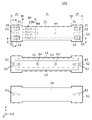
- FIG. 1 is an exploded plan view of the transmission line 101 according to the first embodiment, and is a plan view of three base material layers of a substrate which is a component of the transmission line.
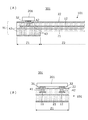
- 2 (A) and 2 (B) are cross-sectional views of the transmission line 101 according to the first embodiment.
- 3A and 3B are cross-sectional views of a circuit board 301 composed of a transmission line 101 and an electronic component 201.
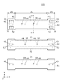
- FIG. 4 is an exploded plan view of the transmission line 102 according to the second embodiment, and is a plan view of three base material layers of a substrate which is a component of the transmission line.
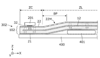
- FIG. 5 is a cross-sectional view of the transmission line 102 according to the second embodiment mounted on a mounting board.
- FIG. 6 is an exploded plan view of the transmission line 103 according to the third embodiment, and is a plan view of the three base material layers of the substrate which is a component of the transmission line.
- FIG. 7 is an exploded plan view of the transmission line 104 according to the fourth embodiment, and is a plan view of the three base material layers of the substrate which is a component of the transmission line.
- FIG. 8 is an exploded plan view of the transmission line 105 according to the fifth embodiment, and is a plan view of the three base material layers of the substrate which is a component of the transmission line.
- FIG. 9 is a cross-sectional view of the transmission line 105 according to the fifth embodiment, and is a cross-sectional view of a YY portion in a state where the three base material layers shown in FIG.
- FIG. 10 is a perspective view of an electronic component 206 which is a multi-pole connector included in the circuit board of the sixth embodiment.
- FIG. 11 is a partial plan view of the transmission line 106 on which the electronic component 206 is mounted, and shows a part of the mounting portion of the electronic component 206.
- FIG. 1 is an exploded plan view of the transmission line according to the first embodiment, and is a plan view of three base material layers of a substrate which is a component of the transmission line.
- 2 (A) and 2 (B) are cross-sectional views of the transmission line 101 according to the first embodiment.
- FIG. 2A is a cross-sectional view of the XX portion in a state where the three base material layers shown in FIG. 1 are laminated
- FIG. 2B is a laminated state of the three base material layers shown in FIG. It is sectional drawing of the YY part in the state.
- the transmission line 101 is configured on the board 91.
- the substrate 91 has flexibility.
- the substrate 91 is a laminate of the four substrate layers S0, S1, S2, and S3 shown in FIG.
- a ground conductor is formed on the entire lower surface of the base material layer S0.
- the first ground conductor 21 is formed on substantially the entire upper surface of the base material layer S1.
- a second ground conductor 22, two first mounting electrodes 31 and two second mounting electrodes 32 are formed on the upper surface of the base material layer S3.
- the second ground conductor 22 and the first mounting electrode 31 are insulated from each other, and the second ground conductor 22 and the second mounting electrode 32 are insulated from each other.
- the base material layers S0, S1, S2, and S3 are, for example, thermoplastic insulating resin sheets before laminating and crimping. Each electrode and conductor is a pattern made of, for example, a copper foil formed on an insulating resin sheet. A resin mother substrate is formed by laminating and heat-pressing resin sheets on which this conductor pattern is formed, and a large number of substrates are formed by dividing the resin sheets.
- the base material layers S0, S1, S2, and S3 may be, for example, a thermoplastic resin layer containing a liquid crystal polymer, PTFE, PFA, or the like. With such a thermoplastic resin layer, the flexibility of the base material layers S0, S1, S2, and S3 can be improved.
- the base material layer S3 is formed with an interlayer connecting conductor 41 that connects the end of the first signal conductor 11 and the first mounting electrode 31. Similarly, an interlayer connecting conductor 42 connecting the end portion of the second signal conductor 12 and the second mounting electrode 32 is formed. Further, the base material layer S3 is formed with interlayer connecting conductors 43 and 44 connecting the second ground conductor 22 and the pad electrodes 53 and 54.
- the base material layer S2 is formed with pad electrodes 53 and 54 that conduct with the interlayer connecting conductors 43 and 44 of the base material layer S3. Further, the base material layer S2 is formed with interlayer connecting conductors 43 and 44 connecting the first ground conductor 21 and the pad electrodes 53 and 54.
- the base material layer S1 is formed with a third interlayer connecting conductor 43 that conducts with the first ground conductor 21.
- the base material layer S0 is formed with a third interlayer connecting conductor 43 that connects the ground conductor on the lower surface and the third interlayer connecting conductor 43 of the base material layer S1.
- both ends of the first signal conductor 11 are connected to the first mounting electrode 31 via the first interlayer connection conductor 41, respectively.
- Both ends of the two signal conductor 12 are connected to the second mounting electrode 32 via the second interlayer connecting conductor 42, respectively.
- the first ground conductor 21 and the second ground conductor 22 are connected via the third interlayer connecting conductor 43, the fourth interlayer connecting conductor 44, and the pad electrodes 53 and 54.
- the first interlayer connection conductor is more than two of the fourth interlayer connection conductors 44 (in the example shown in FIG. 1, since there are only two fourth interlayer connection conductors 44 in the second region Z2 shown later). It is close to 41 and the second interlayer connecting conductor 42. Further, the adjacent distance between the two fourth interlayer connecting conductors 44 is larger than the adjacent distance between the two third interlayer connecting conductors 43.
- the adjacent distance between the third interlayer connection conductors 43 is smaller than 1/2 of the minimum wavelength of the signal transmitted by the first signal conductor 11 and the second signal conductor 12.
- the wavelength is 4.4 mm
- the adjacent distance between the third interlayer connecting conductors 43 is 2.2 mm. Smaller than More preferably, it is smaller than 1.1 mm, which is 1/4 of the minimum wavelength of the signal to be transmitted. More preferably, it is smaller than 0.4 mm, which is 1/10 of the minimum wavelength of the signal to be transmitted.
- the first interlayer connecting conductor 41 is the first ground. It is separated from the conductor 21 and the second ground conductor 22. Therefore, when the third interlayer connecting conductor 43 does not exist, the electromagnetic field is disturbed in the vicinity of the first mounting electrode 31 and the second mounting electrode 32, but the third interlayer connecting conductor 43 is the first mounting electrode. A ground potential portion is formed in the vicinity of the 31 and the second mounting electrode 32, whereby the disturbance of the electromagnetic field in the vicinity of the first mounting electrode 31 and the second mounting electrode 32 is suppressed.
- the substrate 91 includes a first region Z1 in which the first mounting electrode 31 and the second mounting electrode 32 are formed, and a second region Z2 which is another region.
- the first interlayer connecting conductor 41, the second interlayer connecting conductor 42, and the third interlayer connecting conductor 43 are provided in the first region Z1.
- the fourth interlayer connection conductor 44 is provided in the second region Z2.
- the thickness of the second region Z2 (second thickness) is thinner than the thickness of the first region Z1 (first thickness). Therefore, the flexibility of the second region Z2 can be enhanced while maintaining the flatness of the mounting portion.
- the adjacent distance between the third interlayer connecting conductors 43 is smaller than 1/4 of the minimum wavelength of the signal.
- the electromagnetic field of the signal frequency hardly leaks from the gap between the adjacent third interlayer connecting conductors 43, and the isolation between the first interlayer connecting conductor 41 and the second interlayer connecting conductor 42 is sufficient. Is secured in.
- the diameter of the first interlayer connecting conductor 41 is larger than the diameter of the third interlayer connecting conductor 43.
- more third interlayer connection conductors 43 can be arranged in the limited space between the first interlayer connection conductor 41 and the second interlayer connection conductor 42, and a plurality of third interlayer connection conductors can be arranged.
- the effect of arranging 43 is enhanced. Further, by making the diameters of the first interlayer connecting conductor 41 and the second interlayer connecting conductor 42 relatively large, the conductor loss thereof can be reduced, so that the insertion loss of the transmission line can be reduced. Further, the inductance value can be reduced, and the impedance mismatch can be reduced.
- FIG. 3 (A) and 3 (B) are cross-sectional views of a circuit board 301 composed of the transmission line 101 and the electronic component 201.
- the cross-sectional position of the cross-sectional view shown in FIG. 3 (A) corresponds to the cross-sectional position shown in FIG. 2 (A)
- the cross-sectional position of the cross-sectional view shown in FIG. 3 (B) is the cross-sectional position shown in FIG. 2 (B).
- the electronic component 201 is a surface mount type component having two terminals on the bottom surface, and is soldered to the first mounting electrode 31 and the second mounting electrode 32 of the transmission line 101.
- the third interlayer connection conductor 43 is in a region overlapping the outer shape of the electronic component 201 mounted on the substrate 91 via the first mounting electrode 31 and the second mounting electrode 32. In this way, the formation region of the third interlayer connection conductor 43 can be defined by the overlapping region of the electronic components.
- FIGS. 3A and 3B Although one end of the transmission line 101 is shown in FIGS. 3A and 3B, the other end is connected to the circuit board. Further, another electronic component may be mounted on the other end.
- Second Embodiment the transmission line and the circuit board having a different configuration of the second ground conductor 22 from the transmission line shown in the first embodiment are shown.
- FIG. 4 is an exploded plan view of the transmission line 102 according to the second embodiment, and is a plan view of three base material layers of a substrate which is a component of the transmission line.
- the first region Z1 and the second region Z2 are defined by the difference in the thickness of the substrate, but in the second embodiment, the region is defined by the connection region to the mounting substrate and the other transmission line region.
- the area ZC shown in FIG. 4 is a mounting board connection area, and the area ZL is a transmission line area.
- a bent portion BP is provided in the transmission line region ZL.
- the transmission line of the second embodiment has a different configuration of the second ground conductor 22 from the transmission line of the first embodiment.
- the bent portion BP of the transmission line is provided with a mesh-shaped portion 22M on the second ground conductor 22.
- the mesh-shaped portion 22M is a portion in which openings in which a ground conductor is not formed in a mesh shape are arranged vertically and horizontally. Therefore, the mesh-shaped portion 22M has a smaller ground conductor area per unit area than the other portions.
- FIG. 5 is a cross-sectional view of the transmission line 102 according to the second embodiment mounted on a mounting board.
- the mounting board 400 is, for example, a board provided in a portable electronic device.
- the battery 401 is arranged on the mounting board 400.
- the electronic component 201 is mounted in the mounting board connection area ZC of the transmission line 102.
- the circuit board 302 is arranged along the mounting board 400 so as to straddle the upper part of the battery 401.
- the first ground conductor 21 on the lower surface of the transmission line 102 is connected to the ground conductor formed on the upper surface of the mounting board 400.
- the mesh-shaped portion 22M is formed on the second ground conductor 22, but the mesh-shaped portion may be formed on the first ground conductor 21 in the bent portion BP, or the first A mesh-shaped portion may be formed on both the ground conductor 21 and the second ground conductor 22.
- the mounting board connection area ZC at the left end of the transmission line 102 and a part of the transmission line area ZL are shown, but the configuration on the right end side of the transmission line 102 is also the same. Further, the right end side of the transmission line 102 may be connected to a connection electrode formed on the mounting board 400 or another board or device.
- the electronic component 201 may be mounted on the transmission line 102 first to form the circuit board 302, and then the circuit board 302 may be mounted on the mounting board 400, or the transmission line 102 may be mounted on the mounting board 400. Then, the electronic component 201 may be mounted on the transmission line 102.
- the thickness of the transmission line 102 is the same for both the mounting board connection region ZC and the transmission line region ZL, but the mesh-shaped portion 22M has a ground conductor area smaller than the other portions because the ground conductor area per unit area is smaller than the other portions.
- the flexibility of the bent portion BP is high.
- the second ground conductor 22 since the second ground conductor 22 has the mesh-shaped portion 22M in the bent portion BP of the transmission line 102, the flexibility of the bent portion BP is improved.
- Third Embodiment a transmission line having a different configuration of the third interlayer connection conductor 43 from the transmission line shown in the first embodiment is shown.
- FIG. 6 is an exploded plan view of the transmission line 103 according to the third embodiment, and is a plan view of the three base material layers of the substrate which is a component of the transmission line.
- the transmission line according to the third embodiment is configured on the substrate in the same manner as the transmission line shown in the first embodiment.
- This substrate is a laminate of the three base material layers S1, S2, and S3 shown in FIG.
- a first ground conductor 21 is formed on substantially the entire surface of the lower surface of the base material layer S1.
- a first signal conductor 11, a second signal conductor 12, and pad electrodes 53 and 54 running in parallel with each other are formed.
- a second ground conductor 22, two first mounting electrodes 31 and two second mounting electrodes 32 are formed on the upper surface of the base material layer S3.
- the second ground conductor 22 and the first mounting electrode 31 are insulated from each other, and the second ground conductor 22 and the second mounting electrode 32 are insulated from each other.
- the base material layer S3 is formed with a first interlayer connection conductor 41 that connects the end portion of the first signal conductor 11 and the first mounting electrode 31. Similarly, a second interlayer connecting conductor 42 connecting the end portion of the second signal conductor 12 and the second mounting electrode 32 is formed. Further, the base material layer S3 is formed with a third interlayer connecting conductor 43 connecting the second ground conductor 22 and the pad electrode 53 below, and a fourth interlayer connecting conductor 44 connecting the pad electrode 54 below.
- the base material layer S2 is formed with a pad electrode 53 conducting with the third interlayer connecting conductor 43 of the base material layer S3 and a pad electrode 54 conducting with the fourth interlayer connecting conductor 44 of the base material layer S3. Further, the base material layer S2 includes a third interlayer connection conductor 43 that connects the third interlayer connection conductor 43 of the base material layer S1 and the pad electrode 53, and a fourth interlayer connection conductor 44 and the pad electrode of the base material layer S1. A fourth interlayer connecting conductor 44 that connects to 54 is formed.
- the base material layer S1 is formed with a third interlayer connecting conductor 43 and a fourth interlayer connecting conductor 44 that conduct with the first ground conductor 21 on the lower surface.
- the plurality of third interlayer connecting conductors 43 are arranged so as to surround the first interlayer connecting conductor 41 and the second interlayer connecting conductor 42 in the plan view of the substrate. ing.
- a plurality of third interlayer connecting conductors 43 surround the circumference of the first interlayer connecting conductor 41, so that the third interlayer connecting conductor 43 and the first interlayer connecting conductor 41 are pseudo.
- a coaxial line is constructed.
- a plurality of third interlayer connecting conductors 43 surround the second interlayer connecting conductor 42, so that the third interlayer connecting conductor 43 and the second interlayer connecting conductor 42 form a pseudo coaxial line. ..
- the impedance of these coaxial lines can be approximated to the characteristic impedance of the strip line composed of the signal conductors 11 and 12, the first ground conductor 21 and the second ground conductor 22. That is, the impedance mismatch in the vicinity of the first interlayer connecting conductor 41 and the second interlayer connecting conductor 42 can be further suppressed as compared with the case where the number of the third interlayer connecting conductors 43 is small or not.
- FIG. 7 is an exploded plan view of the transmission line 104 according to the fourth embodiment, and is a plan view of the three base material layers of the substrate which is a component of the transmission line.
- the transmission line according to the fourth embodiment is a laminated body of three base material layers S1, S2, and S3, similarly to the transmission line shown in the third embodiment.
- a first ground conductor 21 is formed on substantially the entire surface of the lower surface of the base material layer S1.
- a first signal conductor 11, a second signal conductor 12, and pad electrodes 53 and 54 running in parallel with each other are formed on the upper surface of the base material layer S2.
- a second ground conductor 22, two first mounting electrodes 31 and two second mounting electrodes 32 are formed on the upper surface of the base material layer S3.
- the second ground conductor 22 and the first mounting electrode 31 are insulated from each other, and the second ground conductor 22 and the second mounting electrode 32 are insulated from each other.
- the base material layer S3 is formed with an interlayer connecting conductor 41 that connects the end of the first signal conductor 11 and the first mounting electrode 31. Similarly, an interlayer connecting conductor 42 connecting the end portion of the second signal conductor 12 and the second mounting electrode 32 is formed. Further, the base material layer S3 is formed with interlayer connecting conductors 43 and 44 connecting the second ground conductor 22 and the following pad electrodes 53 and 54.
- the base material layer S2 is formed with pad electrodes 53 and 54 that conduct with the interlayer connecting conductors 43 and 44 of the base material layer S3. Further, in the base material layer S2, interlayer connection conductors 43, 44 connecting the interlayer connection conductors 43, 44 of the base material layer S1 and the pad electrodes 53, 54 are formed.
- the base material layer S1 is formed with interlayer connecting conductors 43 and 44 that conduct with the first ground conductor 21 on the lower surface.
- the substrate includes a mounting region ZM of electronic components mounted via the first mounting electrode 31 and the second mounting electrode 32.
- the mounting area ZM is an area that overlaps the outer shape of the electronic component mounted on the substrate.
- the first interlayer connecting conductor 41, the second interlayer connecting conductor 42, and the third interlayer connecting conductor 43 are located in the mounting region ZM.
- the fourth interlayer connection conductor 44 is located in a region other than the mounting region ZM.
- a transmission line having a configuration different from that of the transmission line shown in the first embodiment is shown for the first ground conductor 21 and the second ground conductor 22.
- FIG. 8 is an exploded plan view of the transmission line 105 according to the fifth embodiment, and is a plan view of the three base material layers of the substrate which is a component of the transmission line.
- FIG. 9 is a cross-sectional view of the transmission line 105 according to the fifth embodiment, and is a cross-sectional view of a YY portion in a state where the three base material layers shown in FIG. 8 are laminated.
- the first ground conductor 21 and the second ground conductor 22 have an opening BH between adjacent fourth interlayer connecting conductors 44.
- the flexibility of the transmission line region ZL is improved by forming the opening BH. Further, when the transmission line 105 is manufactured, gas is generated from the conductor paste for forming the fourth interlayer connection conductor 44, and this gas is easily discharged to the outside of the substrate via the opening BH. That is, gas does not remain between the base materials and inside the substrate, and the deformation of the substrate is suppressed.
- a circuit board including a multi-pole connector as an electronic component will be described. Further, a transmission line including three or more signal conductors will be shown.
- the multi-pole connector is a connector having a plurality of lines.
- FIG. 10 is a perspective view of an electronic component 206 which is a multi-pole connector included in the circuit board of the sixth embodiment.
- FIG. 11 is a partial plan view of the transmission line 106 on which the electronic component 206 is mounted, and shows a part of the mounting portion of the electronic component 206.
- the electronic component 206 shown in FIG. 10 is a multi-pole connector in which a large number of contact electrodes 82 and frame electrodes 83a and 83b are integrated with a resin molded body 81.
- the electronic component 201 is a male multi-pole connector having two rows of ridges.
- the electronic component 206 is mounted on a female multi-pole connector having two rows of grooves.
- the electronic component 206 includes signal terminals T1, T2, T3, ground terminals TG, etc., which are drawn out from the contact electrode 82 to the side of the bottom surface.
- the signal terminal T1 corresponds to the "first signal terminal” in the present invention
- the signal terminal T2 corresponds to the "second signal terminal” in the present invention.
- the transmission line 105 shown in FIG. 11 is provided with a large number of signal conductors such as the first signal conductor 11, the second signal conductor 12, and the third signal conductor 13.
- the first mounting electrode 31, the second mounting electrode 32, the third mounting electrode 33, the plurality of second ground conductors 22, and the like are exposed in the opening of the resist film formed on the surface. ..
- a third interlayer connecting conductor 43 is connected to the exposed portion of each second ground conductor 22.
- the signal terminals T1, T2, and T3 shown in FIG. 10 are connected to the mounting electrodes 31, 32, and 33 shown in FIG. 11, respectively. Further, the plurality of ground terminals TG are each connected to the second ground conductor 22.
- adjacent signal terminals are shielded by a ground conductor 22, a ground terminal TG, and a third interlayer connecting conductor existing between the signal terminals. Therefore, isolation between adjacent transmission lines is ensured. Further, since the third interlayer connecting conductor 43 is formed at the position where the ground terminal TG of the electronic component 206 is connected, the potential difference between the ground terminal TG of the electronic component 206 and the first ground conductor 21 and the second ground conductor 22. Can be made smaller and has high stability as a transmission line.
Landscapes
- Engineering & Computer Science (AREA)
- Microelectronics & Electronic Packaging (AREA)
- Physics & Mathematics (AREA)
- Electromagnetism (AREA)
- Structure Of Printed Boards (AREA)
- Transmission And Conversion Of Sensor Element Output (AREA)
- Measuring Magnetic Variables (AREA)
- Hall/Mr Elements (AREA)
- Production Of Multi-Layered Print Wiring Board (AREA)
Priority Applications (3)
| Application Number | Priority Date | Filing Date | Title |
|---|---|---|---|
| CN202090000823.3U CN217062469U (zh) | 2019-10-02 | 2020-09-29 | 传输线路以及电路基板 |
| JP2021551298A JP7060171B2 (ja) | 2019-10-02 | 2020-09-29 | 伝送線路及び回路基板 |
| US17/694,794 US12080935B2 (en) | 2019-10-02 | 2022-03-15 | Transmission line and circuit board |
Applications Claiming Priority (2)
| Application Number | Priority Date | Filing Date | Title |
|---|---|---|---|
| JP2019181875 | 2019-10-02 | ||
| JP2019-181875 | 2019-10-02 |
Related Child Applications (1)
| Application Number | Title | Priority Date | Filing Date |
|---|---|---|---|
| US17/694,794 Continuation US12080935B2 (en) | 2019-10-02 | 2022-03-15 | Transmission line and circuit board |
Publications (1)
| Publication Number | Publication Date |
|---|---|
| WO2021065883A1 true WO2021065883A1 (ja) | 2021-04-08 |
Family
ID=75338336
Family Applications (1)
| Application Number | Title | Priority Date | Filing Date |
|---|---|---|---|
| PCT/JP2020/036831 Ceased WO2021065883A1 (ja) | 2019-10-02 | 2020-09-29 | 伝送線路及び回路基板 |
Country Status (4)
| Country | Link |
|---|---|
| US (1) | US12080935B2 (https=) |
| JP (1) | JP7060171B2 (https=) |
| CN (1) | CN217062469U (https=) |
| WO (1) | WO2021065883A1 (https=) |
Cited By (1)
| Publication number | Priority date | Publication date | Assignee | Title |
|---|---|---|---|---|
| WO2022242221A1 (zh) * | 2021-05-21 | 2022-11-24 | 荣耀终端有限公司 | 传输组件及可折叠电子设备 |
Families Citing this family (2)
| Publication number | Priority date | Publication date | Assignee | Title |
|---|---|---|---|---|
| JP7197057B2 (ja) * | 2020-05-15 | 2022-12-27 | 株式会社村田製作所 | 伝送線路 |
| US12506282B2 (en) * | 2022-11-24 | 2025-12-23 | Murata Manufacturing Co., Ltd. | Antenna device |
Citations (4)
| Publication number | Priority date | Publication date | Assignee | Title |
|---|---|---|---|---|
| JP2010050627A (ja) * | 2008-08-20 | 2010-03-04 | Toshiba Corp | 高周波多層基板及び高周波多層基板の製造方法 |
| JP2013026601A (ja) * | 2011-07-26 | 2013-02-04 | Mitsubishi Electric Corp | プリント配線板、プリント配線板モジュール、光通信モジュール、光通信装置、および演算処理装置 |
| WO2016163436A1 (ja) * | 2015-04-09 | 2016-10-13 | 株式会社村田製作所 | 複合伝送線路および電子機器 |
| WO2017199930A1 (ja) * | 2016-05-17 | 2017-11-23 | 株式会社村田製作所 | 多層基板、および、電子機器 |
Family Cites Families (2)
| Publication number | Priority date | Publication date | Assignee | Title |
|---|---|---|---|---|
| JPH0586859A (ja) | 1991-09-27 | 1993-04-06 | Mazda Motor Corp | エンジンの冷却装置 |
| JP4462758B2 (ja) * | 2000-12-27 | 2010-05-12 | 京セラ株式会社 | 高周波用配線基板 |
-
2020
- 2020-09-29 JP JP2021551298A patent/JP7060171B2/ja active Active
- 2020-09-29 WO PCT/JP2020/036831 patent/WO2021065883A1/ja not_active Ceased
- 2020-09-29 CN CN202090000823.3U patent/CN217062469U/zh active Active
-
2022
- 2022-03-15 US US17/694,794 patent/US12080935B2/en active Active
Patent Citations (4)
| Publication number | Priority date | Publication date | Assignee | Title |
|---|---|---|---|---|
| JP2010050627A (ja) * | 2008-08-20 | 2010-03-04 | Toshiba Corp | 高周波多層基板及び高周波多層基板の製造方法 |
| JP2013026601A (ja) * | 2011-07-26 | 2013-02-04 | Mitsubishi Electric Corp | プリント配線板、プリント配線板モジュール、光通信モジュール、光通信装置、および演算処理装置 |
| WO2016163436A1 (ja) * | 2015-04-09 | 2016-10-13 | 株式会社村田製作所 | 複合伝送線路および電子機器 |
| WO2017199930A1 (ja) * | 2016-05-17 | 2017-11-23 | 株式会社村田製作所 | 多層基板、および、電子機器 |
Cited By (1)
| Publication number | Priority date | Publication date | Assignee | Title |
|---|---|---|---|---|
| WO2022242221A1 (zh) * | 2021-05-21 | 2022-11-24 | 荣耀终端有限公司 | 传输组件及可折叠电子设备 |
Also Published As
| Publication number | Publication date |
|---|---|
| CN217062469U (zh) | 2022-07-26 |
| JPWO2021065883A1 (https=) | 2021-04-08 |
| US12080935B2 (en) | 2024-09-03 |
| US20220200118A1 (en) | 2022-06-23 |
| JP7060171B2 (ja) | 2022-04-26 |
Similar Documents
| Publication | Publication Date | Title |
|---|---|---|
| US11581622B2 (en) | Transmission line and electronic device | |
| CN204948494U (zh) | 树脂多层基板及电子设备 | |
| JP5754562B1 (ja) | 高周波信号線路及び電子機器 | |
| US9935352B2 (en) | Composite transmission line and electronic device | |
| JP6252699B2 (ja) | 伝送線路およびフラットケーブル | |
| CN205092303U (zh) | 信号传输元器件及电子设备 | |
| JP7060171B2 (ja) | 伝送線路及び回路基板 | |
| JP2014030173A (ja) | フラットケーブルおよび電子機器 | |
| US12389532B2 (en) | High-frequency circuit | |
| WO2015118791A1 (ja) | 高周波信号伝送線路及び電子機器 | |
| US9949368B2 (en) | Resin substrate and electronic device | |
| JP5472552B2 (ja) | 高周波信号線路及び電子機器 | |
| JP4414365B2 (ja) | 高速伝送用基板 | |
| JP6760540B2 (ja) | 伝送線路及びその実装構造 | |
| CN213938408U (zh) | 传输线路及其安装构造 | |
| JP6515817B2 (ja) | 配線基板及び電子機器 | |
| CN223261692U (zh) | 多层基板 | |
| KR20210099766A (ko) | 케이블 모듈 및 이를 제조하기 위한 방법 | |
| CN217363377U (zh) | 传输线路以及电子设备 | |
| JP7768019B2 (ja) | シールドフラットケーブル | |
| CN205211905U (zh) | 传输线路 | |
| JP7823488B2 (ja) | シールドフラットケーブル | |
| JPWO2019017206A1 (ja) | 回路モジュール | |
| WO2023132309A1 (ja) | 伝送線路およびそれを備える電子機器 | |
| WO2026048599A1 (ja) | 多層基板及び電子機器 |
Legal Events
| Date | Code | Title | Description |
|---|---|---|---|
| 121 | Ep: the epo has been informed by wipo that ep was designated in this application |
Ref document number: 20872051 Country of ref document: EP Kind code of ref document: A1 |
|
| ENP | Entry into the national phase |
Ref document number: 2021551298 Country of ref document: JP Kind code of ref document: A |
|
| NENP | Non-entry into the national phase |
Ref country code: DE |
|
| 122 | Ep: pct application non-entry in european phase |
Ref document number: 20872051 Country of ref document: EP Kind code of ref document: A1 |