WO2021059581A1 - 圧電振動子及びその製造方法 - Google Patents
圧電振動子及びその製造方法 Download PDFInfo
- Publication number
- WO2021059581A1 WO2021059581A1 PCT/JP2020/019308 JP2020019308W WO2021059581A1 WO 2021059581 A1 WO2021059581 A1 WO 2021059581A1 JP 2020019308 W JP2020019308 W JP 2020019308W WO 2021059581 A1 WO2021059581 A1 WO 2021059581A1
- Authority
- WO
- WIPO (PCT)
- Prior art keywords
- layer
- electrode
- piezoelectric
- crystal
- electrodes
- Prior art date
- Legal status (The legal status is an assumption and is not a legal conclusion. Google has not performed a legal analysis and makes no representation as to the accuracy of the status listed.)
- Ceased
Links
Images





Classifications
-
- H—ELECTRICITY
- H10—SEMICONDUCTOR DEVICES; ELECTRIC SOLID-STATE DEVICES NOT OTHERWISE PROVIDED FOR
- H10N—ELECTRIC SOLID-STATE DEVICES NOT OTHERWISE PROVIDED FOR
- H10N30/00—Piezoelectric or electrostrictive devices
- H10N30/80—Constructional details
- H10N30/87—Electrodes or interconnections, e.g. leads or terminals
- H10N30/875—Further connection or lead arrangements, e.g. flexible wiring boards, terminal pins
-
- H—ELECTRICITY
- H03—ELECTRONIC CIRCUITRY
- H03H—IMPEDANCE NETWORKS, e.g. RESONANT CIRCUITS; RESONATORS
- H03H9/00—Networks comprising electromechanical or electro-acoustic elements; Electromechanical resonators
- H03H9/02—Details
- H03H9/05—Holders or supports
- H03H9/10—Mounting in enclosures
- H03H9/1007—Mounting in enclosures for bulk acoustic wave [BAW] devices
- H03H9/1014—Mounting in enclosures for bulk acoustic wave [BAW] devices the enclosure being defined by a frame built on a substrate and a cap, the frame having no mechanical contact with the BAW device
- H03H9/1021—Mounting in enclosures for bulk acoustic wave [BAW] devices the enclosure being defined by a frame built on a substrate and a cap, the frame having no mechanical contact with the BAW device the BAW device being of the cantilever type
-
- H—ELECTRICITY
- H03—ELECTRONIC CIRCUITRY
- H03H—IMPEDANCE NETWORKS, e.g. RESONANT CIRCUITS; RESONATORS
- H03H3/00—Apparatus or processes specially adapted for the manufacture of impedance networks, resonating circuits, resonators
- H03H3/007—Apparatus or processes specially adapted for the manufacture of impedance networks, resonating circuits, resonators for the manufacture of electromechanical resonators or networks
- H03H3/02—Apparatus or processes specially adapted for the manufacture of impedance networks, resonating circuits, resonators for the manufacture of electromechanical resonators or networks for the manufacture of piezoelectric or electrostrictive resonators or networks
-
- H—ELECTRICITY
- H03—ELECTRONIC CIRCUITRY
- H03H—IMPEDANCE NETWORKS, e.g. RESONANT CIRCUITS; RESONATORS
- H03H3/00—Apparatus or processes specially adapted for the manufacture of impedance networks, resonating circuits, resonators
- H03H3/007—Apparatus or processes specially adapted for the manufacture of impedance networks, resonating circuits, resonators for the manufacture of electromechanical resonators or networks
- H03H3/02—Apparatus or processes specially adapted for the manufacture of impedance networks, resonating circuits, resonators for the manufacture of electromechanical resonators or networks for the manufacture of piezoelectric or electrostrictive resonators or networks
- H03H3/04—Apparatus or processes specially adapted for the manufacture of impedance networks, resonating circuits, resonators for the manufacture of electromechanical resonators or networks for the manufacture of piezoelectric or electrostrictive resonators or networks for obtaining desired frequency or temperature coefficient
-
- H—ELECTRICITY
- H03—ELECTRONIC CIRCUITRY
- H03H—IMPEDANCE NETWORKS, e.g. RESONANT CIRCUITS; RESONATORS
- H03H9/00—Networks comprising electromechanical or electro-acoustic elements; Electromechanical resonators
- H03H9/02—Details
- H03H9/05—Holders or supports
- H03H9/0504—Holders or supports for bulk acoustic wave devices
- H03H9/0514—Holders or supports for bulk acoustic wave devices consisting of mounting pads or bumps
- H03H9/0519—Holders or supports for bulk acoustic wave devices consisting of mounting pads or bumps for cantilever
-
- H—ELECTRICITY
- H03—ELECTRONIC CIRCUITRY
- H03H—IMPEDANCE NETWORKS, e.g. RESONANT CIRCUITS; RESONATORS
- H03H9/00—Networks comprising electromechanical or electro-acoustic elements; Electromechanical resonators
- H03H9/15—Constructional features of resonators consisting of piezoelectric or electrostrictive material
- H03H9/17—Constructional features of resonators consisting of piezoelectric or electrostrictive material having a single resonator
- H03H9/19—Constructional features of resonators consisting of piezoelectric or electrostrictive material having a single resonator consisting of quartz
-
- H—ELECTRICITY
- H03—ELECTRONIC CIRCUITRY
- H03H—IMPEDANCE NETWORKS, e.g. RESONANT CIRCUITS; RESONATORS
- H03H3/00—Apparatus or processes specially adapted for the manufacture of impedance networks, resonating circuits, resonators
- H03H3/007—Apparatus or processes specially adapted for the manufacture of impedance networks, resonating circuits, resonators for the manufacture of electromechanical resonators or networks
- H03H3/02—Apparatus or processes specially adapted for the manufacture of impedance networks, resonating circuits, resonators for the manufacture of electromechanical resonators or networks for the manufacture of piezoelectric or electrostrictive resonators or networks
- H03H3/04—Apparatus or processes specially adapted for the manufacture of impedance networks, resonating circuits, resonators for the manufacture of electromechanical resonators or networks for the manufacture of piezoelectric or electrostrictive resonators or networks for obtaining desired frequency or temperature coefficient
- H03H2003/0414—Resonance frequency
- H03H2003/0485—Resonance frequency during the manufacture of a cantilever
Definitions
- the present invention relates to a piezoelectric vibrator and a method for manufacturing the same.
- Piezoelectric oscillators are used in various electronic devices such as mobile communication terminals, communication base stations, and home appliances for applications such as timing devices, sensors, and oscillators.
- the piezoelectric vibrator includes a piezoelectric vibrating element having a mechanical vibrating portion that converts electric vibration into mechanical vibration by utilizing the piezoelectric effect, a cage accommodating the piezoelectric vibrating element, and a piezoelectric vibrating element and a cage. It consists of a conductive holding member that is electrically connected.
- the conductive holding member is, for example, a cured product of a conductive adhesive containing a silicone resin as a main component.
- Patent Document 1 describes a siloxane that evaporates from a silicone-based adhesive by chemically adsorbing silicone molecules on the entire surface of an excitation electrode in which gold is formed on the surface layer of a piezoelectric substrate using chromium as a base film to form a monomolecular film.
- a method of preventing the components from adhering to the entire surface of the excitation electrode and suppressing the frequency fluctuation of the piezoelectric vibrator is disclosed.
- the chromium in the base film diffuses and rises from the grain boundaries of the gold particles in the process of manufacturing the piezoelectric vibrator, and the chromium exposed from the monomolecular film is oxidized or hydroxylated.
- the frequency may fluctuate.
- the present invention has been made in view of such circumstances, and an object of the present invention is to provide a piezoelectric vibrator having improved frequency stability and a method for manufacturing the same.
- the piezoelectric vibrator includes a piezoelectric vibrating element having a piezoelectric piece and a pair of electrodes including electrodes facing each other across the piezoelectric piece, and a cage accommodating the piezoelectric vibrating element.
- a resin layer is provided above at least one of the pair of electrodes, and a water-repellent layer having a lower moisture permeability than the resin layer is provided between the electrodes.
- the method for manufacturing a piezoelectric vibrator includes a step of preparing a piezoelectric piece, a step of providing a pair of electrodes including electrodes facing each other across the piezoelectric piece, and a conductive holding member.
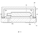
- FIG. 1 is an exploded perspective view schematically showing the configuration of the crystal oscillator according to the first embodiment.
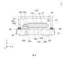
- FIG. 2 is a cross-sectional view schematically showing the configuration of the crystal oscillator according to the first embodiment.
- Each drawing is provided with a Cartesian coordinate system consisting of the X-axis, Y'axis and Z'axis for convenience to clarify the relationship between the drawings and to help understand the positional relationship of each member.
- the X-axis, Y'axis and Z'axis correspond to each other in the drawings.
- the X-axis, Y'axis, and Z'axis correspond to the crystallographic axes of the crystal piece 11 described later, respectively.
- the X-axis corresponds to the electric axis (polar axis)
- the Y-axis corresponds to the mechanical axis
- the Z-axis corresponds to the optical axis.
- the Y'axis and the Z'axis are axes obtained by rotating the Y axis and the Z axis around the X axis in the direction of the Y axis to the Z axis by 35 degrees 15 minutes ⁇ 1 minute 30 seconds, respectively.
- the direction parallel to the X-axis is referred to as "X-axis direction”
- the direction parallel to the Y'axis is referred to as “Y'axis direction”
- the direction parallel to the Z'axis is referred to as "Z'axis direction”.
- the direction of the tip of the arrow on the X-axis, Y'axis, and Z'axis is called “+ (plus)”, and the direction opposite to the arrow is called “-(minus)”.
- the + Y'axis direction is defined as an upward direction
- the ⁇ Y'axis direction is defined as a downward direction, but the vertical direction of the crystal oscillator 1 is not limited.
- the + Y'axis direction side of the crystal vibrating element 10 is the upper surface 11A
- the ⁇ Y'axis direction side is the lower surface 11B. It may be arranged so as to be located vertically below.
- the crystal oscillator 1 includes a crystal vibrating element 10, a base member 30, a lid member 40, and a joining member 50.
- the crystal vibrating element 10 is provided between the base member 30 and the lid member 40.
- the base member 30, the lid member 40, and the joining member 50 form a cage for accommodating the crystal vibrating element 10.
- the base member 30 has a flat plate shape
- the lid member 40 has a bottomed opening for accommodating the crystal vibrating element 10 on the base member 30 side.
- the crystal vibrating element 10 is mounted on the base member 30.
- the shapes of the base member 30 and the lid member 40 are not limited to the above as long as at least the excited portion of the crystal vibrating element 10 is housed in the cage.
- the method of holding the crystal vibrating element 10 is not limited to the above.
- the base member 30 may have a bottomed opening for accommodating the crystal vibrating element 10 on the lid member 40 side. Further, the base member 30 and the lid member 40 may sandwich the peripheral portion of the excited portion of the crystal vibrating element 10.
- the crystal vibrating element 10 is an element that vibrates a crystal by a piezoelectric effect and converts electrical energy and mechanical energy.
- the crystal vibrating element 10 includes a flaky crystal piece 11, a first excitation electrode 14a and a second excitation electrode 14b constituting a pair of excitation electrodes, and a first extraction electrode 15a and a second extraction electrode forming a pair of extraction electrodes. It includes an electrode 15b, and a first connection electrode 16a and a second connection electrode 16b forming a pair of connection electrodes.
- the crystal piece 11 has an upper surface 11A and a lower surface 11B facing each other.
- the upper surface 11A is located on the side opposite to the side facing the base member 30, that is, the side facing the top surface portion 41 of the lid member 40 described later.
- the lower surface 11B is located on the side facing the base member 30.
- the crystal piece 11 is, for example, an AT-cut type crystal piece.
- the AT-cut type crystal piece 11 is a plane parallel to a plane specified by the X-axis and the Z'axis in a Cartesian coordinate system consisting of an X-axis, a Y'axis, and a Z'axis that intersect each other (hereinafter, "XZ". It is called a'plane'. The same applies to a plane specified by another axis.) Is the main surface, and is formed so that the direction parallel to the Y'axis is the thickness.
- the AT-cut type crystal piece 11 is formed by etching a crystal substrate (for example, a crystal wafer) obtained by cutting and polishing a crystal of artificial quartz (Synthetic Quartz Crystal).
- the crystal vibrating element 10 using the AT-cut type crystal piece 11 has high frequency stability in a wide temperature range.
- the thickness slip vibration mode Thiickness Shear Vibration Mode
- the rotation angles of the Y'axis and the Z'axis of the AT-cut type crystal piece 11 may be tilted in the range of 35 degrees 15 minutes to ⁇ 5 degrees or more and 15 degrees or less.
- a different cut other than the AT cut may be applied.
- BT cut, GT cut, SC cut and the like may be applied.
- the crystal vibrating element may be a tuning fork type crystal vibrating element using a crystal piece having a cut angle called a Z plate.
- the AT-cut type crystal piece 11 is parallel to the long side direction in which the long side parallel to the X-axis direction extends, the short side direction in which the short side parallel to the Z'axis direction extends, and the Y'axis direction. It is a plate shape having a thickness direction in which a large thickness extends.
- the crystal piece 11 has a rectangular shape when the upper surface 11A is viewed in a plan view, and has an excitation unit 17 located at the center and contributing to excitation, and peripheral portions 18 and 19 adjacent to the excitation unit 17. ..
- the excitation portion 17 and the peripheral portions 18 and 19 are each formed in a band shape over the entire width along the Z'axis direction of the crystal piece 11.
- the peripheral portion 18 is located on the ⁇ X-axis direction side of the excitation portion 17, and the peripheral portion 19 is located on the + X-axis direction side of the excitation portion 17.
- the planar shape of the crystal piece 11 when the upper surface 11A is viewed in a plane is not limited to a rectangular shape.
- the planar shape of the crystal piece 11 may be a polygonal shape, a circular shape, an elliptical shape, or a combination thereof.
- the planar shape of the crystal piece 11 may be a tuning fork shape.
- the crystal piece 11 may have a base and a vibrating arm extending in parallel from the base.
- a slit may be formed in the crystal piece 11 for the purpose of suppressing vibration leakage and stress propagation.
- the shapes of the exciting portion 17 and the peripheral portions 18 and 19 of the crystal piece 11 are not limited to the strip shape over the entire width.
- the planar shape of the excitation portion may be an island shape adjacent to the peripheral portion in the Z'axis direction, and the planar shape of the peripheral portion may be formed in a frame shape surrounding the excitation portion.
- the crystal piece 11 has a so-called mesa-shaped structure in which the thickness of the exciting portion 17 is larger than the thickness of the peripheral portions 18 and 19. According to the crystal piece 11 having a mesa-shaped structure, vibration leakage from the exciting portion 17 can be suppressed.
- the crystal piece 11 has a double-sided mesa-shaped structure, and the excitation portions 17 project from the peripheral portions 18 and 19 on both sides of the upper surface 11A and the lower surface 11B.
- the boundary between the exciting portion 17 and the peripheral portion 18 and the boundary between the exciting portion 17 and the peripheral portion 19 form a tapered shape in which the thickness changes continuously, but a staircase shape in which the change in thickness is discontinuous. May be good.
- the boundary may have a convex shape in which the amount of change in thickness changes continuously, or a bevel shape in which the amount of change in thickness changes discontinuously.
- the crystal piece 11 may have a single-sided mesa-shaped structure in which the exciting portion 17 projects from the peripheral portions 18 and 19 on one side of the upper surface 11A or the lower surface 11B. Further, the crystal piece 11 may have a so-called inverted mesa type structure in which the thickness of the exciting portion 17 is smaller than the thickness of the peripheral portions 18 and 19.
- the first excitation electrode 14a and the second excitation electrode 14b are provided in the excitation unit 17.
- the first excitation electrode 14a is provided on the upper surface 11A side of the crystal piece 11, and the second excitation electrode 14b is provided on the lower surface 11B side of the crystal piece 11.
- the first excitation electrode 14a is provided on the main surface of the crystal piece 11 on the lid member 40 side
- the second excitation electrode 14b is provided on the main surface of the crystal piece 11 on the base member 30 side.
- the first excitation electrode 14a and the second excitation electrode 14b face each other with the crystal piece 11 interposed therebetween.
- the first excitation electrode 14a and the second excitation electrode 14b each have a rectangular shape, and are arranged so that substantially the entire surface of the crystal piece 11 overlaps with each other.
- the first excitation electrode 14a and the second excitation electrode 14b are each formed in a band shape over the entire width along the Z'axis direction of the crystal piece 11.
- Each of the first excitation electrode 14a and the second excitation electrode 14b constituting the pair of electrodes corresponds to the electrodes facing each other with the crystal piece 11 interposed therebetween.
- planar shapes of the first excitation electrode 14a and the second excitation electrode 14b when the upper surface 11A of the crystal piece 11 is viewed in a plan view are not limited to a rectangular shape.
- the planar shape of the first excitation electrode 14a and the second excitation electrode 14b may be a polygonal shape, a circular shape, an elliptical shape, or a combination thereof.
- the first extraction electrode 15a and the second extraction electrode 15b are provided on the peripheral portion 18.
- the first extraction electrode 15a is provided on the upper surface 11A side of the crystal piece 11, and the second extraction electrode 15b is provided on the lower surface 11B side of the crystal piece 11.
- the first extraction electrode 15a electrically connects the first excitation electrode 14a and the first connection electrode 16a.
- the second extraction electrode 15b electrically connects the second excitation electrode 14b and the second connection electrode 16b.
- one end of the first extraction electrode 15a is connected to the first excitation electrode 14a in the excitation portion 17, and the other end of the first extraction electrode 15a is connected to the first connection electrode 16a in the peripheral portion 18. Has been done.
- one end of the second extraction electrode 15b is connected to the second excitation electrode 14b at the excitation portion 17, and the other end of the second extraction electrode 15b is connected to the second connection electrode 16b at the peripheral portion 18.
- the first extraction electrode 15a and the second extraction electrode 15b are separated from each other when the upper surface 11A of the crystal piece 11 is viewed in a plan view.
- the first extraction electrode 15a is provided in the + Z'axis direction when viewed from the second extraction electrode 15b.
- the first connection electrode 16a and the second connection electrode 16b are electrodes for electrically connecting the first excitation electrode 14a and the second excitation electrode 14b to the base member 30, respectively, and the peripheral portion 18 of the crystal piece 11 It is provided on the lower surface 11B side.
- the first connection electrode 16a is provided at a corner formed by an end portion of the crystal piece 11 on the ⁇ X axis direction side and an end portion on the + Z ′ axis direction side
- the second connection electrode 16b is the crystal piece 11 of the crystal piece 11. It is provided at a corner formed by an end portion on the -X-axis direction side and an end portion on the -Z'axis direction side.
- the base member 30 holds the crystal vibrating element 10 in an excitable manner.
- the base member 30 includes a substrate 31 having an upper surface 31A and a lower surface 31B facing each other.
- the upper surface 31A is located on the side of the crystal vibrating element 10 and the lid member 40, and corresponds to a mounting surface on which the crystal vibrating element 10 is mounted.
- the lower surface 31B corresponds to, for example, a mounting surface facing the circuit board when the crystal oscillator 1 is mounted on an external circuit board.
- the substrate 31 is a sintered material such as an insulating ceramic (alumina). From the viewpoint of suppressing the generation of thermal stress, the substrate 31 is preferably made of a heat-resistant material. From the viewpoint of suppressing the stress applied to the crystal vibrating element 10 by the thermal history, the substrate 31 may be provided by a material having a coefficient of thermal expansion close to that of the crystal piece 11, or may be provided by, for example, quartz.
- the base member 30 includes a first electrode pad 33a and a second electrode pad 33b that form a pair of electrode pads.
- the first electrode pad 33a and the second electrode pad 33b are provided on the upper surface 31A of the substrate 31.
- the first electrode pad 33a and the second electrode pad 33b are terminals for electrically connecting the crystal vibrating element 10 to the base member 30.
- the first electrode pad 33a and the second electrode pad 33b may have a two-layer structure having a base layer for improving adhesion to the substrate 31 and a surface layer containing gold and suppressing oxidation.
- the base member 30 includes a first external electrode 35a, a second external electrode 35b, a third external electrode 35c, and a fourth external electrode 35d.
- the first external electrode 35a to the fourth external electrode 35d are provided on the lower surface 31B of the substrate 31.
- the first external electrode 35a and the second external electrode 35b are terminals for electrically connecting an external substrate (not shown) and the crystal oscillator 1.
- the third external electrode 35c and the fourth external electrode 35d are dummy electrodes to which electric signals and the like are not input / output, but may be ground electrodes for improving the electromagnetic shielding function of the lid member 20 by grounding the lid member 40. ..
- the third external electrode 35c and the fourth external electrode 35d may be omitted.
- the first electrode pad 33a and the second electrode pad 33b are aligned along the Z'axis direction at the end of the base member 30 on the ⁇ X axis direction side.
- the first external electrode 35a and the second external electrode 35b are aligned along the Z'axis direction at the end of the base member 30 on the ⁇ X axis direction side.
- the third external electrode 35c and the fourth external electrode 35d are aligned along the Z'axis direction at the end of the base member 30 on the + X axis direction.
- the first electrode pad 33a is electrically connected to the first external electrode 35a via the first through electrode 34a that penetrates the substrate 31 along the Y'axis direction.
- the second electrode pad 33b is electrically connected to the second external electrode 35b via the second through electrode 34b that penetrates the substrate 31 along the Y'axis direction.
- the first electrode pad 33a and the second electrode pad 33b are electrically connected to the first external electrode 35a and the second external electrode 35b via the side electrodes provided on the side surfaces connecting the upper surface 31A and the lower surface 31B of the substrate 31, respectively. May be connected.
- the first external electrode 35a to the fourth external electrode 35d may be a casting electrode provided in a concave shape on the side surface of the substrate 31.
- the base member 30 includes a first conductive holding member 36a and a second conductive holding member 36b that form a pair of conductive holding members.
- the first conductive holding member 36a and the second conductive holding member 36b mount the crystal vibrating element 10 on the base member 30, and electrically connect the crystal vibrating element 10 and the base member 30.
- the first conductive holding member 36a is joined to the first electrode pad 33a and the first connection electrode 16a, and electrically connects the first electrode pad 33a and the first connection electrode 16a.
- the second conductive holding member 36b is joined to the second electrode pad 33b and the second connection electrode 16b, and electrically connects the second electrode pad 33b and the second connection electrode 16b.
- the first conductive holding member 36a and the second conductive holding member 36b hold the crystal vibrating element 10 at intervals from the base member 30 so that the exciting portion 17 can be excited.
- the first conductive holding member 36a and the second conductive holding member 36b are cured products of a conductive adhesive containing a thermosetting resin, a photocurable resin, and the like, and the first conductive holding member 36a and the second conductive.
- the main component of the property-retaining member 36b is, for example, a silicone resin.
- the first conductive holding member 36a and the second conductive holding member 36b contain conductive particles, and as the conductive particles, for example, metal particles containing silver (Ag) are used.
- the first conductive holding member 36a adheres the first electrode pad 33a and the first connecting electrode 16a
- the second conductive holding member 36b adheres the second electrode pad 33b and the second connecting electrode 16b.
- the main components of the first conductive holding member 36a and the second conductive holding member 36b are not limited to silicone resin as long as they are curable resins, and may be, for example, epoxy resin or acrylic resin. Further, the imparting of conductivity to the first conductive holding member 36a and the second conductive holding member 36b is not limited to that by silver particles, and other metals, conductive ceramics, conductive organic materials, etc. It may be due to.
- the main components of the first conductive holding member 36a and the second conductive holding member 36b may be a conductive polymer.
- any additive may be contained in the resin composition of the first conductive holding member 36a and the second conductive holding member 36b.
- the additive is, for example, a tackifier, a filler, a thickener, a sensitizer, an antiaging agent, an antifoaming agent, etc. for the purpose of improving the workability and storage stability of the conductive adhesive.
- a filler may be added for the purpose of increasing the strength of the cured product or for maintaining the distance between the base member 30 and the crystal vibrating element 10.
- the lid member 40 is joined to the base member 30 to form an internal space 49 in which the crystal vibrating element 10 is housed with the base member 30.
- the material of the lid member 40 is not particularly limited, but is made of a conductive material such as metal. Since the lid member 40 is made of a conductive material, the lid member 40 is provided with an electromagnetic shield function that reduces the ingress and egress of electromagnetic waves into the internal space 49.
- the lid member 40 has a flat top surface portion 41 and a side wall portion 42 that is connected to the outer edge of the top surface portion 41 and extends in a direction intersecting the main surface of the top surface portion 41.
- the planar shape of the top surface portion 41 when viewed in a plane from the normal direction of the main surface is, for example, a rectangular shape.
- the top surface portion 41 faces the base member 30 with the crystal vibrating element 10 in between, and the side wall portion 42 surrounds the crystal vibrating element 10 in a direction parallel to the XZ'plane.
- the tip of the side wall portion 42 extends in a frame shape on the base member 30 side of the crystal vibrating element 10.
- the lid member 40 may be provided of a ceramic material, a semiconductor material, a resin material, or the like. Further, the planar shape of the top surface portion 41 may be a polygonal shape, a circular shape, an elliptical shape, or a combination thereof.
- the joining member 50 is provided over the entire circumference of each of the base member 30 and the lid member 40, and has a rectangular frame shape.
- the first electrode pad 33a and the second electrode pad 33b are arranged inside the joining member 50, and the joining member 50 is provided so as to surround the crystal vibrating element 10. ing.
- the joining member 50 joins the tip of the side wall portion 42 of the lid member 40 and the upper surface 31A of the base 31 of the base member 30 to seal the internal space 49.
- the joining member 50 is made of a resin material.
- the joining member 50 preferably has a high gas barrier property, and more preferably has a low moisture permeability.
- Such a joining member 50 is, for example, a cured product of an adhesive containing an epoxy resin as a main component.
- the resin-based adhesive constituting the joining member 50 may contain, for example, a polyimide resin, a vinyl compound, an acrylic compound, a urethane compound, a silicone compound, or the like.
- the joining member 50 is not limited to a frame shape that is continuous in the circumferential direction, and may be provided discontinuously in the circumferential direction.
- the joining member 50 may be provided by a cured product of a silicon-based adhesive containing water glass or the like, a cured product of a calcium-based adhesive containing cement or the like, an Au—Sn alloy-based metal solder, or the like.
- a metallized layer may be provided on the base member 30 for the purpose of improving the adhesion between the base member 30 and the joining member 50.
- the joining member 50 may include a cured product of the resin-based adhesive and a coating having a lower moisture permeability than the cured product of the resin-based adhesive.
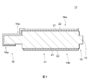
- FIG. 3 is a cross-sectional view schematically showing the configuration of the electrodes of the crystal vibrating element.
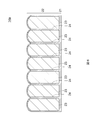
- FIG. 4 is a plan view schematically showing the structure of the surface at the central portion of the first excitation electrode.
- the crystal vibrating element 10 includes a pair of electrodes.
- one of the pair of electrodes includes a first excitation electrode 14a, a first extraction electrode 15a, and a first connection electrode 16a
- the other electrode of the pair of electrodes is a second excitation. It includes an electrode 14b, a second extraction electrode 15b, and a second connection electrode 16b.
- a group of electrodes including the first excitation electrode 14a, the first extraction electrode 15a, and the first connection electrode 16a are formed continuously with each other. In this case, the group of electrodes may be integrally formed.
- a group of electrodes including the second excitation electrode 14b, the second extraction electrode 15b, and the second connection electrode 16b are formed continuously with each other and may be integrally formed.
- the pair of electrodes of the crystal vibrating element 10 has a base layer 21 and a surface layer 22.
- the base layer 21 is in contact with the crystal piece 11, and is provided between the crystal piece 11 and the surface layer 22.
- the base layer 21 is provided with a material having a higher adhesion to the crystal piece 11 than the material of the surface layer 22.
- the base layer 21 contains chromium (Cr) as a main component.
- the base layer 21 is, for example, a Cr film formed on the surface of the crystal piece 11 by a sputtering method.
- the base layer 21 corresponds to the first layer of the first excitation electrode 14a and the second excitation electrode 14b.
- the main component of the base layer 21 is not limited to Cr as long as it has a high affinity for silicon oxide, and may be nickel (Ni) or the like.
- the surface layer 22 is provided on the side of the base layer 21 opposite to the crystal vibrating element 10.
- the thickness of the surface layer 22 is larger than the thickness of the base layer 21.
- the surface layer 22 is provided with a material having a higher chemical stability than the material of the base layer 21.
- the surface layer 22 contains gold (Au) as a main component.
- the surface layer 22 is, for example, an Au film formed on the surface of the base layer 21 by a sputtering method.
- the thickness of the surface layer 22 of the first excitation electrode 14a is larger than the thickness of the surface layer 22 of the second excitation electrode 14b.
- the central portion on the XZ'plane may be scraped deeper than the periphery. That is, the surface of the first excitation electrode 14a may have a concave shape at the central portion on the XZ'plane.
- the thickness of the surface layer 22 of the first excitation electrode 14a may be substantially uniform.
- the surface layer 22 is a polycrystal in which a plurality of crystal grains 23 are aggregated.
- Each grain boundary 24 of the plurality of crystal grains 23 serves as a diffusion path for chromium diffused from the base layer 21.
- Each of the plurality of crystal grains 23 has an interface portion 25 located in the vicinity of the grain boundary 24 and a surface portion 26 surrounded by the interface portion 25.
- the interface portion 25 is raised more than the surface portion 26. Further, the interface portion 25 is covered with the chromium compound 27. Therefore, as shown in FIG.
- the surface of the first excitation electrode 14a is composed of a mesh-shaped chromium compound 27 and a surface portion 26 of a plurality of crystal grains 23 surrounded by the chromium compound 27.
- the chromium compound 27 is obtained by diffusing the chromium of the base layer 21 through the grain boundaries of the surface layer 22 and oxidizing it on the surface of the surface layer 22, and is chromium oxide or a hydrate thereof.
- the inventors speculated that the reason why the frequency fluctuates in the subsequent heating step is that the chromium newly diffused from the grain boundaries 24 lifts the chromium compound 27 and the chromium exposed from the vicinity of the interface portion 25 is oxidized. .. In order to suppress the formation of the chromium compound 27, it is desirable to inhibit the contact between chromium and water.
- a water-repellent layer L1 and a resin layer L2 are provided on the surface of the first excitation electrode 14a.
- the resin layer L2 traps the moisture in the atmosphere of the crystal vibrating element 10 and prevents the moisture from reaching the first excitation electrode 14a.
- the water-repellent layer L1 inhibits the penetration of water from the resin layer L2 into the first excitation electrode 14a.
- the water repellent layer L1 and the resin layer L2 are also provided on the surface of the second excitation electrode 14b.
- the water-repellent layer L1 and the resin layer L2 may be provided on at least one surface of the first excitation electrode 14a and the second excitation electrode 14b, and preferably are provided on both surfaces.
- the water-repellent layer L1 is provided between the surface layer 22 and the resin layer L2, and is in contact with the surface of the first excitation electrode 14a.
- the water-repellent layer L1 has a lower moisture permeability than the resin layer L2.
- the water repellent layer L1 is provided by, for example, a hydrophobic resin material.
- the material constituting the water-repellent layer L1 includes, for example, a silicone resin.
- the water-repellent layer L1 is provided in a region including a grain boundary 24. In other words, the water-repellent layer L1 is provided at least above the interface portion 25 and covers the chromium compound 27.
- the water-repellent layer L1 preferably covers the surface of the first excitation electrode 14a.
- the water-repellent layer L1 preferably continuously covers the surface portion 26 and the chromium compound 27 constituting the surface of the first excitation electrode 14a.
- the thickness of the water-repellent layer L1 on the surface portion 26 is larger than the thickness of the water-repellent layer L1 on the chromium compound 27.
- the resin layer L2 is provided above the surface layer 22 and is in contact with the surface of the water repellent layer L1.
- the resin layer L2 is provided by, for example, a resin material having high heat resistance.
- the material constituting the resin layer L2 includes, for example, an epoxy resin or a polyimide resin.
- the thickness of the resin layer L2 is larger than the thickness of the water repellent layer L1.
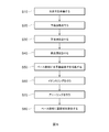
- FIG. 5 is a flowchart schematically showing a method for manufacturing a crystal oscillator according to the first embodiment.
- FIG. 6 is a cross-sectional view schematically showing the first excitation electrode before performing ion milling.
- FIG. 7 is a cross-sectional view schematically showing a change in the first excitation electrode due to ion milling.
- FIG. 8 is a cross-sectional view schematically showing a change in the conductive holding member due to annealing.
- FIG. 9 is a cross-sectional view schematically showing a change in the first excitation electrode due to annealing.
- FIG. 10 is a cross-sectional view schematically showing a change in the joining member in the joining step.
- FIG. 11 is a cross-sectional view schematically showing a change in the first excitation electrode in the joining step.
- a crystal piece is prepared (S10).
- a crystal substrate is cut out from the crystal body of the artificial quartz so that the XZ'plane is the main surface.
- a part of the crystal substrate is removed by wet etching using a photolithography method to form the contour of the crystal piece 11 when the XZ'plane is viewed in a plane.
- a part of the peripheral portions 18 and 19 of the crystal piece 11 is removed by wet etching, and the crystal piece 11 is shaped into a double-sided mesa type structure.
- the method for forming and shaping the crystal piece 11 is not limited to wet etching, and may be performed by using, for example, dry etching.
- the crystal piece 11 may be individualized by dicing the crystal substrate, or the individualized crystal piece 11 may be beveled.
- This step includes a step S20 for preheating, a step S30 for providing the base layer 21, and a step S40 for providing the surface layer 22.
- step S20 for preheating the crystal piece 11 is heated to 150 ° C. or higher and 300 ° C. or lower.
- the temperature of the crystal piece 11 is lower than 150 ° C., the average particle size of the crystal grains 23 of the surface layer 22 becomes small, and the diffusion of chromium becomes easy to proceed. Even with the grain growth by annealing described later, the crystal grains cannot be sufficiently grown.
- the temperature of the crystal piece 11 is higher than 300 ° C., the diffusion of chromium is superior to the suppression of the diffusion of chromium due to grain growth, and the amount of chromium raised on the surface of the excitation electrode increases.
- the step S20 for preheating may be omitted.
- the water-repellent layer L1 and the resin layer L2 inhibit the bond between chromium and water raised on the electrode surface. Therefore, even if the base layer 21 and the surface layer 22 are provided without preheating, it is possible to sufficiently suppress the change in mass of the exciting portion 17 of the crystal vibrating element 10 with time.
- a pattern is formed using a metal mask by a sputtering method.
- chromium is used as the sputtering target, and chromium is deposited on the surface of the preheated crystal piece 11 to form the base layer 21 of the electrode pattern.
- the thickness of the base layer 21 is, for example, 5 nm.
- gold is used as the sputtering target, and gold is deposited on the surface of the base layer 21 to form the surface layer 22 of the electrode pattern.
- the plurality of crystal grains 23 grow in columns from the base layer 21. Chrome diffuses on the surfaces of the grain boundaries 24 and the crystal grains 23.
- the thickness of the surface layer 22 on the upper surface 11A side of the crystal piece 11 is, for example, 140 nm.
- the surface layer 22 is provided so that the thickness of the crystal piece 11 on the upper surface 11A side is larger than the thickness on the lower surface 11B side.
- the step S30 for providing the base layer 21 and the step S40 for providing the surface layer 22 are pattern forming using a metal mask, the heat capacity of the metal mask is large. It is difficult to raise the temperature. Therefore, the step S20 for preheating is performed in the front chamber of the film forming chamber.
- the preheating may be performed in the film forming chamber, during the film formation of at least one of the base layer 21 and the surface layer 22, or between the film formation of the base layer 21 and the film formation of the surface layer 22. May be good.
- the step of providing the electrode on the surface of the crystal piece 11 is not limited to the pattern film formation. After forming the base layer 21 and the surface layer 22 on the entire surface of the crystal piece 11, a part of the base layer 21 and the surface layer 22 may be removed by etching to form an electrode pattern.
- the film forming method of the base layer 21 and the surface layer 22 is not limited to the sputtering method, and may be appropriately selected from various vapor deposition methods such as PVD (Physical Vapor Deposition) and CVD (Chemical Vapor Deposition). Good. Further, the base layer 21 and the surface layer 22 may be formed by a film forming method other than the vapor deposition method such as a printing method or a plating method.
- the crystal vibration element is mounted on the base member (S50).
- a paste-like resin composition which is a material of the first conductive holding member 36a and the second conductive holding member 36b is applied onto the first electrode pad 33a and the second electrode pad 33b of the base member 30.
- the crystal vibrating element 10 is placed on the resin composition, and the resin composition is cured to form the first conductive holding member 36a and the second conductive holding member 36b.
- the resin composition of the first conductive holding member 36a and the second conductive holding member 36b may be applied to the crystal vibration element 10 in advance.
- step S60 ion milling is performed (S60). As shown in FIG. 7, at least a part of the surface of the first excitation electrode 14a is irradiated with an ion beam BM to remove a part of the surface layer 22. As a result, the mass of the exciting portion 17 of the crystal vibrating element 10 is changed, and the frequency of the crystal vibrating element 10 is adjusted. That is, the step S60 corresponds to the frequency adjustment step. Specifically, a voltage is applied to the first excitation electrode 14a and the second excitation electrode 14b to monitor the frequency, a part of the first excitation electrode 14a is removed, and the frequency is gradually increased to the target frequency.
- the rate of gold removal by the ion beam BM is higher than the rate of removal of chromium. Therefore, at the end of step S60, the interface portion 25 is raised above the surface portion 26 due to the influence of chromium diffused through the grain boundary 24 as a path.
- annealing is performed (S70).
- the lattice defects formed in the plurality of crystal grains 23 by ion milling are reduced by annealing, and the plurality of crystal grains 23 are recrystallized. Further, the recrystallized plurality of crystal grains 23 are grain-grown or, as shown in FIG. 9, adjacent crystal grains 23 are fused. As a result, the particle size of each of the plurality of crystal grains 23 is increased, and the grain boundaries, which are the diffusion paths of chromium, are reduced.
- each electrode is annealed, and a part of the conductive holding member is scattered and deposited on the surface of each electrode.
- the resin particles 36p scattered from the first conductive holding member 36a are deposited on the surface of the first excitation electrode 14a to form the water-repellent layer L1.
- the resin particles 36p also scatter from the second conductive holding member 36b and are also deposited on the surface of the second excitation electrode 14b. Since the water-repellent layer L1 is formed by the resin particles 36p derived from the pair of conductive holding members 36a and 36b, the pair of conductive holding members 36a and 36b have the same material as the material constituting the water-repellent layer L1. ..
- the thickness of the water-repellent layer L1 is, for example, about several nm to 10 nm.
- heat treatment at 240 ° C. for 6 hours is carried out in a nitrogen atmosphere.
- the lid member is joined to the base member (S80).
- a paste-like resin composition which is a material of the joining member 50, is applied to the tip of the side wall portion 42 of the lid member 40.
- the resin composition is sandwiched between the base member 30 and the lid member 40, and the resin composition is cured to form the joining member 50.
- the lid member 40 is joined to the base member 30, and a part of the joining member 50 is scattered and deposited on the water-repellent layer L1.
- the resin particles 50p scattered from the joining member 50 are deposited on the surface of the water-repellent layer L1 formed on the surface of the first excitation electrode 14a to form the resin layer L2.
- the resin particles 50p are also deposited on the surface of the water-repellent layer L1 formed on the surface of the second excitation electrode 14b. Since the resin layer L2 is formed by the resin particles 50p derived from the bonding member 50, the bonding member 50 has the same material as the material constituting the resin layer L2.
- the thickness of the resin layer L2 is, for example, about several nm to 50 nm.
- the step of forming the water-repellent layer L1 may be performed separately from the step of performing annealing. Further, the step of forming the resin layer L2 may be performed separately from the step of joining the lid member 40 to the base member 30. For example, it may be carried out before the step S50 in which the crystal vibrating element 10 is mounted on the base member 30, or between the step S50 and the step S70 for annealing.
- Each method of forming the water-repellent layer L1 and the resin layer L2 is not limited to the so-called dry process in which resin particles are deposited.
- Each of the water-repellent layer L1 and the resin layer L2 may be formed by a wet process such as printing.
- the crystal oscillator includes a crystal vibrating element having a crystal piece, a pair of electrodes including electrodes facing each other, and a cage for accommodating the crystal vibrating element, and a pair.
- a resin layer is provided above at least one of the electrodes, and a water-repellent layer having a lower moisture permeability than the resin layer is provided between the electrodes. According to this, the resin layer traps the moisture in the atmosphere of the crystal vibration element and hinders the arrival of the moisture to the electrode, and the water repellent layer inhibits the permeation of the moisture from the resin layer to the electrode.
- the mass change of the exciting portion of the crystal vibrating element is caused by the reversible moisture absorption and drying of the resin layer, and the irreversible mass change of the exciting portion due to the oxidation and hydroxylation of the electrode can be inhibited. Therefore, fluctuations in frequency over time can be suppressed.
- the crystal oscillator further comprises a pair of conductive holding members that hold the quartz vibrating element in the cage, and the pair of conductive holding members have the same material as the material constituting the water repellent layer. According to this, by forming the water-repellent layer with the material derived from the conductive holding member, the conductive holding member and the water-repellent layer can be formed at the same time, and the manufacturing process can be simplified.
- the material constituting the water-repellent layer contains a silicone resin. According to this, even if the electrode surface is deformed, such as a ridge due to diffusion of the underlying layer, the water-repellent layer is less likely to be damaged and the moisture permeability is less likely to decrease.
- the cage has a base member, a lid member that forms an internal space for accommodating the crystal vibrating element between the base member, and a joining member that joins the base member and the lid member.
- the joining member is made of a resin material. Sealing the cage with a resin material can reduce manufacturing costs as compared to sealing with a metal material, but reduces airtightness. Therefore, the chromium expressed on the surface of the electrode is oxidized by the invasion of water vapor to form a hydrate, and the frequency is likely to fluctuate due to the change in the mass of the electrode. However, according to the present embodiment, even in the case of sealing with a resin material, the mass change of the electrode can be suppressed and the frequency fluctuation can be suppressed.
- the joining member has the same material as the material constituting the resin layer. According to this, by forming the resin layer with the material derived from the joining member, the joining member and the water-repellent layer can be formed at the same time, and the manufacturing process can be simplified.
- the material constituting the resin layer includes an epoxy resin or a polyimide resin. According to this, since the resin layer is formed of a heat-resistant resin material, the film formation rate of the dry process is slowed down, and the resin layer can be thinned. As a result, the mass change of the exciting portion due to moisture absorption and drying of the resin layer can be suppressed. In addition, damage to the resin layer during heat treatment after forming the resin layer, such as reflow when mounting the crystal unit, can be suppressed. Damage to the water-repellent layer during the heat treatment can be suppressed, and a decrease in moisture resistance can be suppressed.
- At least one of the pair of electrodes has a first layer containing gold and a second layer containing chromium provided between the crystal piece and the first layer, and the water repellent layer is: It is provided in the region including the gold grain boundary in the first layer. According to this, since the water-repellent layer covers the gold grain boundaries that serve as the diffusion path of chromium, the oxidation and hydroxylation of chromium can be efficiently inhibited.
- At least one of the pair of electrodes has an excitation electrode, and the water repellent layer covers the surface of the excitation electrode.
- the water-repellent layer covers the entire surface of the excitation electrode, the permeation of water through the interface between the excitation electrode and the water-repellent layer can be inhibited.
- the surface of the excitation electrode is composed of the surface portion of gold crystal grains and the exposed chromium
- the water-repellent layer covers the surface portion, so that the water adhering to the surface portion becomes the surface portion and the water-repellent layer. It can be prevented from penetrating through the interface of and coming into contact with chromium.
- the method for manufacturing a crystal oscillator includes a step of preparing a crystal piece, a step of providing a pair of electrodes including electrodes facing each other across the crystal piece, and a conductive holding member.
- the embodiment according to the present invention is not limited to the crystal oscillator, and can be applied to the piezoelectric oscillator.
- An example of a piezoelectric oscillator is a quartz crystal oscillator (Quartz Crystal Resonator Unit) provided with a crystal vibrating element (Quartz Crystal Resonator).
- the crystal vibrating element uses a crystal piece (Quartz Crystal Element) as the piezoelectric piece excited by the piezoelectric effect, and the piezoelectric piece is arbitrary such as a piezoelectric single crystal, a piezoelectric ceramic, a piezoelectric thin film, or a piezoelectric polymer film. It may be formed by the piezoelectric material of.
- the piezoelectric single crystal can include lithium niobate (LiNbO 3 ).
- the piezoelectric ceramic is barium titanate (BaTiO 3), lead titanate (PbTiO 3), lead zirconate titanate (Pb (Zr x Ti 1- x) O3; PZT), aluminum nitride (AlN), niobium Lithium acid (LiNbO 3 ), lithium metaniobate (LiNb 2 O 6 ), bismuth titanate (Bi 4 Ti 3 O 12 ) lithium tantalate (LiTaO 3 ), lithium tetraborate (Li 2 B 4 O 7 ), Langa Sight (La 3 Ga 5 SiO 14 ), tantalate pentoxide (Ta 2 O 5 ), and the like can be mentioned.
- Examples of the piezoelectric thin film include those obtained by forming the above-mentioned piezoelectric ceramic on a substrate such as quartz or sapphire by a sputtering method or the like.
- Examples of the piezoelectric polymer membrane include polylactic acid (PLA), polyvinylidene fluoride (PVDF), and vinylidene fluoride / ethylene trifluoride (VDF / TrFE) copolymer.
- PVA polylactic acid
- PVDF polyvinylidene fluoride
- VDF / TrFE vinylidene fluoride / ethylene trifluoride copolymer.
- the above-mentioned various piezoelectric materials may be used by being laminated with each other, or may be laminated with another member.
- the embodiment according to the present invention is appropriately applicable without particular limitation as long as it is a device that converts electromechanical energy by a piezoelectric effect, such as a timing device, a sounding device, an oscillator, and a load sensor.
Landscapes
- Physics & Mathematics (AREA)
- Acoustics & Sound (AREA)
- Engineering & Computer Science (AREA)
- Manufacturing & Machinery (AREA)
- Piezo-Electric Or Mechanical Vibrators, Or Delay Or Filter Circuits (AREA)
Priority Applications (3)
| Application Number | Priority Date | Filing Date | Title |
|---|---|---|---|
| CN202080056557.0A CN114208028A (zh) | 2019-09-26 | 2020-05-14 | 压电振子及其制造方法 |
| JP2021548325A JP7273377B2 (ja) | 2019-09-26 | 2020-05-14 | 圧電振動子及びその製造方法 |
| US17/651,483 US12376497B2 (en) | 2019-09-26 | 2022-02-17 | Piezoelectric vibrator and manufacturing method therefor |
Applications Claiming Priority (2)
| Application Number | Priority Date | Filing Date | Title |
|---|---|---|---|
| JP2019-175977 | 2019-09-26 | ||
| JP2019175977 | 2019-09-26 |
Related Child Applications (1)
| Application Number | Title | Priority Date | Filing Date |
|---|---|---|---|
| US17/651,483 Continuation US12376497B2 (en) | 2019-09-26 | 2022-02-17 | Piezoelectric vibrator and manufacturing method therefor |
Publications (1)
| Publication Number | Publication Date |
|---|---|
| WO2021059581A1 true WO2021059581A1 (ja) | 2021-04-01 |
Family
ID=75166005
Family Applications (1)
| Application Number | Title | Priority Date | Filing Date |
|---|---|---|---|
| PCT/JP2020/019308 Ceased WO2021059581A1 (ja) | 2019-09-26 | 2020-05-14 | 圧電振動子及びその製造方法 |
Country Status (4)
| Country | Link |
|---|---|
| US (1) | US12376497B2 (https=) |
| JP (1) | JP7273377B2 (https=) |
| CN (1) | CN114208028A (https=) |
| WO (1) | WO2021059581A1 (https=) |
Citations (3)
| Publication number | Priority date | Publication date | Assignee | Title |
|---|---|---|---|---|
| JPS57107624A (en) * | 1980-12-25 | 1982-07-05 | Seikosha Co Ltd | Piezoelectric oscillator |
| JP2003198312A (ja) * | 2001-12-25 | 2003-07-11 | Seiko Epson Corp | 圧電デバイスとその製造方法、及び圧電デバイスを利用した携帯電話装置ならびに圧電デバイスを利用した電子機器 |
| JP2010232806A (ja) * | 2009-03-26 | 2010-10-14 | Seiko Epson Corp | 圧電振動子、圧電発振器、電子機器、及び圧電振動子の製造方法 |
Family Cites Families (11)
| Publication number | Priority date | Publication date | Assignee | Title |
|---|---|---|---|---|
| JPS62165421A (ja) * | 1986-01-16 | 1987-07-22 | Murata Mfg Co Ltd | 電子部品およびその製造方法 |
| JPH07308317A (ja) * | 1994-05-17 | 1995-11-28 | Olympus Optical Co Ltd | 超音波探触子 |
| JPH1141051A (ja) * | 1997-07-16 | 1999-02-12 | Matsushita Electric Ind Co Ltd | 圧電共振部品およびその製造方法 |
| WO2004105237A1 (ja) * | 2003-05-26 | 2004-12-02 | Murata Manufacturing Co., Ltd. | 圧電電子部品、およびその製造方法、通信機 |
| JP5070674B2 (ja) * | 2004-06-14 | 2012-11-14 | 富士ゼロックス株式会社 | インクジェット記録ヘッド、及びインクジェット記録装置 |
| JP4852850B2 (ja) | 2005-02-03 | 2012-01-11 | セイコーエプソン株式会社 | 圧電振動素子、圧電振動子、圧電発振器、周波数安定化方法、及び圧電振動子の製造方法 |
| US7794063B2 (en) * | 2006-03-15 | 2010-09-14 | Brother Kogyo Kabushiki Kaisha | Liquid-droplet jetting head and liquid-droplet jetting apparatus |
| JP2009207068A (ja) * | 2008-02-29 | 2009-09-10 | Kyocera Kinseki Corp | 圧電デバイス |
| JP5346182B2 (ja) * | 2008-07-30 | 2013-11-20 | 富士フイルム株式会社 | 体腔内超音波探触子 |
| CN103460376B (zh) * | 2011-04-11 | 2016-02-17 | 株式会社村田制作所 | 电子部件以及电子部件的制造方法 |
| US9881741B2 (en) * | 2014-12-11 | 2018-01-30 | Murata Manufacturing Co., Ltd. | Multilayer ceramic electronic component |
-
2020
- 2020-05-14 WO PCT/JP2020/019308 patent/WO2021059581A1/ja not_active Ceased
- 2020-05-14 CN CN202080056557.0A patent/CN114208028A/zh active Pending
- 2020-05-14 JP JP2021548325A patent/JP7273377B2/ja active Active
-
2022
- 2022-02-17 US US17/651,483 patent/US12376497B2/en active Active
Patent Citations (3)
| Publication number | Priority date | Publication date | Assignee | Title |
|---|---|---|---|---|
| JPS57107624A (en) * | 1980-12-25 | 1982-07-05 | Seikosha Co Ltd | Piezoelectric oscillator |
| JP2003198312A (ja) * | 2001-12-25 | 2003-07-11 | Seiko Epson Corp | 圧電デバイスとその製造方法、及び圧電デバイスを利用した携帯電話装置ならびに圧電デバイスを利用した電子機器 |
| JP2010232806A (ja) * | 2009-03-26 | 2010-10-14 | Seiko Epson Corp | 圧電振動子、圧電発振器、電子機器、及び圧電振動子の製造方法 |
Also Published As
| Publication number | Publication date |
|---|---|
| JP7273377B2 (ja) | 2023-05-15 |
| US12376497B2 (en) | 2025-07-29 |
| US20220199892A1 (en) | 2022-06-23 |
| CN114208028A (zh) | 2022-03-18 |
| JPWO2021059581A1 (https=) | 2021-04-01 |
Similar Documents
| Publication | Publication Date | Title |
|---|---|---|
| JP2001196883A (ja) | 圧電共振素子の周波数調整方法 | |
| US12160221B2 (en) | Piezoelectric resonator unit and method of manufacturing the same | |
| US8664837B2 (en) | Piezoelectric device and method for fabricating the same | |
| US8319404B2 (en) | Surface-mountable quartz-crystal devices and methods for manufacturing same | |
| US8341814B2 (en) | Methods for manufacturing piezoelectric devices | |
| US12476610B2 (en) | Piezoelectric vibrator and manufacturing method therefor | |
| US20130278114A1 (en) | Piezoelectric device and method for fabricating the same | |
| US11689177B2 (en) | Electronic device and manufacturing method therefor | |
| WO2021044663A1 (ja) | パッケージ構造及びその製造方法 | |
| JP7465454B2 (ja) | 圧電振動素子、圧電振動子及び電子装置 | |
| JP7273377B2 (ja) | 圧電振動子及びその製造方法 | |
| US20230268904A1 (en) | Resonator device and method of manufacturing resonator device | |
| JP2016144091A (ja) | 振動子の製造方法 | |
| JP7462882B2 (ja) | 圧電振動子及びその製造方法 | |
| JP7465458B2 (ja) | 圧電振動子 | |
| US20220173709A1 (en) | Piezoelectric vibrator | |
| JP7497754B2 (ja) | 圧電振動子及びその製造方法 | |
| WO2021095294A1 (ja) | 圧電振動子及びその製造方法 | |
| JP2021175139A (ja) | 圧電振動子及びその製造方法 | |
| WO2021220542A1 (ja) | 圧電振動子 | |
| WO2021215040A1 (ja) | 圧電振動子 | |
| JP2008048144A (ja) | 圧電デバイス用蓋体、及びこれを利用した圧電デバイス、並びに圧電デバイスの製造方法 |
Legal Events
| Date | Code | Title | Description |
|---|---|---|---|
| 121 | Ep: the epo has been informed by wipo that ep was designated in this application |
Ref document number: 20868568 Country of ref document: EP Kind code of ref document: A1 |
|
| ENP | Entry into the national phase |
Ref document number: 2021548325 Country of ref document: JP Kind code of ref document: A |
|
| NENP | Non-entry into the national phase |
Ref country code: DE |
|
| 122 | Ep: pct application non-entry in european phase |
Ref document number: 20868568 Country of ref document: EP Kind code of ref document: A1 |