WO2021044478A1 - イオン性化合物、有機エレクトロニクス材料、有機層、有機エレクトロニクス素子、有機エレクトロルミネセンス素子、表示素子、照明装置、及び有機エレクトロニクス素子の製造方法 - Google Patents
イオン性化合物、有機エレクトロニクス材料、有機層、有機エレクトロニクス素子、有機エレクトロルミネセンス素子、表示素子、照明装置、及び有機エレクトロニクス素子の製造方法 Download PDFInfo
- Publication number
- WO2021044478A1 WO2021044478A1 PCT/JP2019/034408 JP2019034408W WO2021044478A1 WO 2021044478 A1 WO2021044478 A1 WO 2021044478A1 JP 2019034408 W JP2019034408 W JP 2019034408W WO 2021044478 A1 WO2021044478 A1 WO 2021044478A1
- Authority
- WO
- WIPO (PCT)
- Prior art keywords
- group
- organic
- ionic compound
- charge
- layer
- Prior art date
- Legal status (The legal status is an assumption and is not a legal conclusion. Google has not performed a legal analysis and makes no representation as to the accuracy of the status listed.)
- Ceased
Links
- CXPMSVJQCPZIMZ-UHFFFAOYSA-N C=CC[N+](CC=C)(CC=C)[O-] Chemical compound C=CC[N+](CC=C)(CC=C)[O-] CXPMSVJQCPZIMZ-UHFFFAOYSA-N 0.000 description 1
- VMZBNIRXGJODON-UHFFFAOYSA-N c(cc1)ccc1S(c1ccccc1)(c1ccccc1)c1ccccc1 Chemical compound c(cc1)ccc1S(c1ccccc1)(c1ccccc1)c1ccccc1 VMZBNIRXGJODON-UHFFFAOYSA-N 0.000 description 1
- WQAMHDCAVKWLMX-UHFFFAOYSA-N c1ccc([B](c2ccccc2)(c2ccccc2)c2ccccc2)cc1 Chemical compound c1ccc([B](c2ccccc2)(c2ccccc2)c2ccccc2)cc1 WQAMHDCAVKWLMX-UHFFFAOYSA-N 0.000 description 1
Images
Classifications
-
- H—ELECTRICITY
- H10—SEMICONDUCTOR DEVICES; ELECTRIC SOLID-STATE DEVICES NOT OTHERWISE PROVIDED FOR
- H10K—ORGANIC ELECTRIC SOLID-STATE DEVICES
- H10K50/00—Organic light-emitting devices
- H10K50/10—OLEDs or polymer light-emitting diodes [PLED]
- H10K50/11—OLEDs or polymer light-emitting diodes [PLED] characterised by the electroluminescent [EL] layers
-
- C—CHEMISTRY; METALLURGY
- C07—ORGANIC CHEMISTRY
- C07C—ACYCLIC OR CARBOCYCLIC COMPOUNDS
- C07C211/00—Compounds containing amino groups bound to a carbon skeleton
- C07C211/01—Compounds containing amino groups bound to a carbon skeleton having amino groups bound to acyclic carbon atoms
- C07C211/20—Compounds containing amino groups bound to a carbon skeleton having amino groups bound to acyclic carbon atoms of an acyclic unsaturated carbon skeleton
- C07C211/21—Monoamines
-
- C—CHEMISTRY; METALLURGY
- C07—ORGANIC CHEMISTRY
- C07C—ACYCLIC OR CARBOCYCLIC COMPOUNDS
- C07C211/00—Compounds containing amino groups bound to a carbon skeleton
- C07C211/62—Quaternary ammonium compounds
- C07C211/63—Quaternary ammonium compounds having quaternised nitrogen atoms bound to acyclic carbon atoms
Definitions
- An embodiment of the present invention relates to an ionic compound, an organic electronic material, an organic layer, an organic electronic element, an organic electroluminescence element, a display element, a lighting device, and a method for manufacturing an organic electronic element.
- Organic electronics devices are devices that perform electrical operations using organic substances, and are expected to exhibit features such as energy saving, low cost, and flexibility, and are attracting attention as a technology that replaces conventional silicon-based inorganic semiconductors. Has been done.
- organic electronic devices include organic electroluminescence devices (hereinafter, also referred to as organic EL devices), organic photoelectric conversion devices, and organic transistors.
- organic EL devices organic electroluminescence devices
- organic photoelectric conversion devices organic photoelectric conversion devices
- organic transistors organic transistors
- organic EL devices are attracting attention as large-area solid-state light source applications as alternatives to, for example, incandescent lamps and gas-filled lamps. It is also attracting attention as the most promising self-luminous display that can replace the liquid crystal display (LCD) in the flat panel display (FPD) field, and its commercialization is progressing.
- LCD liquid crystal display
- FPD flat panel display
- Organic EL devices are roughly classified into two types, low-molecular-weight organic EL devices and high-molecular-weight organic EL devices, according to the organic materials used.
- a high molecular weight material is used as the organic material
- a low molecular weight material is used in the low molecular weight organic EL device.
- high-molecular-weight organic EL devices can be easily formed by wet processes such as printing and inkjet. It is expected as an indispensable element for EL displays.
- an organic EL device manufactured by a wet process using a polymer material has the features that it is easy to reduce the cost and increase the area.
- an organic EL device containing a thin film produced by using a conventional polymer material is desired to be further improved in the characteristics of the organic EL device such as driving voltage, luminous efficiency, and luminous life.
- high-temperature baking is required in the process of drying the solvent in the production of the organic EL device, high-temperature process resistance is also desired for each material.
- the present invention has been made in view of the above, and the embodiment of the present invention is an organic electronic material that can be used for an organic electronic element having excellent element characteristics, and an excellent heat resistance that can be used for the organic electronic material. It is an object of the present invention to provide an ionic compound. Another embodiment aims to provide an organic layer using the organic electronic material, and an organic electronic device, an organic electroluminescence device, a display element, and a lighting device including the organic layer. Furthermore, another embodiment aims to provide a method for manufacturing an organic electronic device using the organic electronic material.
- One embodiment of the present invention relates to an ionic compound containing an ammonium cation and an anion represented by the following formula (1a).
- Ra , R b and R c each independently represent a hydrogen atom or a monovalent organic group, and at least two selected from Ra , R b and R c are monovalent organic.
- a group, at least one selected from Ra , R b and R c is an organic group containing a double bond.
- Another embodiment of the present invention relates to an organic electronics material containing the ionic compound and the charge transporting compound.
- Another embodiment of the present invention relates to an organic layer formed by using the organic electronic material.
- Another embodiment of the present invention relates to an organic electronic device provided with the organic layer.
- Another embodiment of the present invention relates to an organic electroluminescence device provided with the organic layer.
- Another embodiment of the present invention relates to a display element including the organic electroluminescence element.
- another embodiment of the present invention relates to a lighting device including the organic electroluminescence element.
- another embodiment of the present invention relates to a display element including the lighting device and a liquid crystal element as a display means.
- another embodiment of the present invention relates to a method for manufacturing an organic electronic element, which comprises a step of forming an organic layer by a coating method using the organic electronic material.
- an organic electronic material that can be used for an organic electronic device having excellent element characteristics, and an ionic compound that can be used for the organic electronic material and has excellent heat resistance. Further, according to another embodiment of the present invention, it is possible to provide an organic layer using the organic electronic material, and an organic electronic device, an organic electroluminescence device, a display element, and a lighting device including the organic layer. .. Further, according to another embodiment of the present invention, it is possible to provide a method for manufacturing an organic electronic device using the organic electronic material.
- the ionic compound the organic electronics material, the organic layer, the organic electronics element, the organic electroluminescence element, the display element, and the lighting device according to the embodiment of the present invention will be described in detail.
- the embodiment of the present invention is as follows.
- Ra , R b and R c each independently represent a hydrogen atom or a monovalent organic group, and at least two selected from Ra , R b and R c are monovalent organic.
- a group, at least one selected from Ra , R b and R c is an organic group containing a double bond.
- ⁇ 4> The ionic compound according to any one of ⁇ 1> to ⁇ 3>, wherein the organic group has 4 or less carbon atoms in each of Ra , R b, and R c.
- the organic group containing the double bond is any one of ⁇ 1> to ⁇ 4> selected from the group consisting of a vinyl group, a propenyl group, an isopropenyl group, a butenyl group, and an isobutenyl group. Or the ionic compound according to item 1.
- ⁇ 6> The ionic compound according to any one of ⁇ 1> to ⁇ 5>, which contains only one organic group containing the double bond.
- ⁇ 7> The item according to any one of ⁇ 1> to ⁇ 5>, which contains two or more organic groups containing the double bond, and each of the organic groups containing the double bond is the same as each other. Ionic compounds according to.
- E 1 represents an oxygen atom
- E 2 represents a nitrogen atom
- E 3 represents a carbon atom
- E 4 represents a boron atom or a gallium atom
- E 5 represents a phosphorus atom or an antimony atom
- Y 1 ⁇ Y 6 independently represent a single bond or a divalent linking group
- R 1 to R 16 each independently represent an electron-attracting monovalent group (R 2 and R 3 , R 4 to R 6).
- At least two groups selected from, at least two groups selected from R 7 to R 10 , and at least two groups selected from R 11 to R 16 may each be attached to each other.
- the charge transporting compound has at least one unit selected from the group consisting of a unit containing an aromatic amine structure, a unit containing a carbazole structure, and a unit containing a thiophene structure.
- An organic electronic device provided with the organic layer according to ⁇ 15> and ⁇ 14>.
- An organic electroluminescence device provided with the organic layer according to ⁇ 19> and ⁇ 14>.
- ⁇ 23> The organic electroluminescence device according to any one of ⁇ 19> to ⁇ 22>, which has a white emission color.
- ⁇ 24> The organic electroluminescence device according to any one of ⁇ 19> to ⁇ 23>, further comprising a substrate, wherein the substrate has flexibility.
- the organic electroluminescence device according to any one of ⁇ 19> to ⁇ 23>, further comprising a substrate, wherein the substrate is a resin film.
- a display device including the organic electroluminescence device according to any one of ⁇ 26> and ⁇ 19> to ⁇ 25>.
- a lighting device provided with the organic electroluminescence element according to any one of ⁇ 19> to ⁇ 25>.
- a display element including the lighting device according to ⁇ 28> and ⁇ 27> and a liquid crystal element as a display means.
- a method for manufacturing an organic electronic device which comprises a step of forming an organic layer by a coating method using the organic electronic material according to ⁇ 13>.
- the ionic compound of this embodiment comprises an ammonium cation and an anion represented by the following formula, which will be described later. Hereinafter, ammonium cations and anions will be described.
- the ionic compound of the present embodiment is preferably used as a dopant for organic electronic materials.
- the charge-transporting polymer contains a polymerizable functional group
- the ionic compound of the present embodiment is preferably used as a polymerization initiator.
- ammonium cation (Ammonium cation)
- the ammonium cation of the ionic compound of this embodiment is represented by the following formula (1a).
- Ra , R b and R c each independently represent a hydrogen atom or a monovalent organic group, and at least two selected from Ra , R b and R c are monovalent organic. It is the basis.
- the monovalent organic group include an alkyl group, an alkenyl group, an alkynyl group, an aryl group, a heteroaryl group, an arylalkyl group and the like. These groups may further have a substituent, and examples of the substituent include an alkyl group, and an alkyl group having 1 to 10 carbon atoms is preferable. At least two of R a , R b and R c may be bonded to each other to form a ring.
- R a , R b and R c may be the same or different from each other. Further, at least one selected from Ra , R b and R c is an organic group containing a double bond. Examples of the organic group containing a double bond include an alkenyl group and the like.
- the organic group means an atomic group having one or more carbon atoms.
- the aryl group means an atomic group obtained by removing one hydrogen atom from an aromatic hydrocarbon.
- the aromatic hydrocarbon include a monocyclic ring, a condensed ring, or a polycyclic ring in which two or more selected from an independent monocyclic ring and a condensed ring are bonded via a single bond.
- the heteroaryl group refers to an atomic group obtained by removing one hydrogen atom from an aromatic heterocycle. Examples of the aromatic heterocycle include a monocyclic ring, a condensed ring, or a polycyclic ring in which two or more selected from an independent monocyclic ring and a condensed ring are bonded via a single bond.
- R a , R b, and R c Specific examples of R a , R b, and R c will be described, but the present invention is not limited to the following.
- the alkyl group may be linear, branched or cyclic, and may have a substituent.
- the alkyl group preferably has 1 to 24 carbon atoms, more preferably 2 to 18 carbon atoms.
- Specific examples of the alkyl group include a methyl group, an ethyl group, a propyl group, an i-propyl group, a butyl group, an i-butyl group, a t-butyl group, a pentyl group, a hexyl group, a cyclohexyl group, a heptyl group and an octyl group.
- 2-Ethylhexyl group nonyl group, decyl group, dodecyl group, tetradecyl group, octadecyl group, 3,7-dimethyloctyl group, lauryl group, trifluoromethyl group, pentafluoroethyl group, perfluorobutyl group, perfluorohexyl group , Perfluorooctyl group and the like.
- the alkenyl group may be linear, branched or cyclic, and may have a substituent.
- the alkenyl group preferably has 2 to 12, more preferably 2 to 8, and even more preferably 2 to 6.
- Specific examples of the alkenyl group include vinyl group, 1-propenyl group, 2-propenyl group, isopropenyl group, 1-butenyl group, 2-butenyl group, 3-butenyl group, 1-octenyl group and 1-decenyl group. Examples include 1-octadecenyl group.
- the alkynyl group may be linear, branched or cyclic, and may have a substituent.
- the carbon number of the alkynyl group is preferably 2 to 12, more preferably 2 to 8, and even more preferably 2 to 6.
- Specific examples of the alkynyl group include ethynyl group, 1-propynyl group, 2-propynyl group, 1-butynyl group, 2-butynyl group, 3-butynyl group, 1-octynyl group, 1-decynyl group and 1-octadecynyl group. And so on.
- the aryl group may further have a substituent, and examples of the substituent include an alkyl group, and an alkyl group having 1 to 10 carbon atoms is preferable.
- the monovalent aryl group in the unsubstituted state preferably has 6 to 60 carbon atoms, more preferably 6 to 30 carbon atoms, and further preferably 6 to 18 carbon atoms.
- a phenyl group, a C1 to C12 alkoxyphenyl group (C1 to C12 indicate that the substituent has 1 to 12 carbon atoms; the same applies hereinafter), a C1 to C12 alkylphenyl group, Examples thereof include 1-naphthyl group, 2-naphthyl group, 1-anthrasenyl group, 2-anthrasenyl group, 9-anthrasenyl group, phenanthrene-yl group, pyrene-yl group, perylene-yl group, pentafluorophenyl group and the like.
- C1-C12 alkyl examples include methyl, ethyl, propyl, i-propyl, butyl, i-butyl, t-butyl, pentyl, hexyl, cyclohexyl, heptyl, octyl, 2-ethylhexyl, nonyl, decyl, 3 , 7-Dimethyloctyl, lauryl and the like are exemplified.
- the heteroaryl group may further have a substituent, and examples of the substituent include an alkyl group, and an alkyl group having 1 to 10 carbon atoms is preferable.
- the monovalent heteroaryl group in the unsubstituted state preferably has 4 to 60 carbon atoms, more preferably 4 to 40 carbon atoms, and further preferably 4 to 20 carbon atoms.
- a thienyl group, a C1 to C12 alkylthenyl group, a pyrrolyl group, a frill group, a pyridyl group, a C1 to C12 alkylpyridyl group and the like are exemplified, and a thienyl group, a C1 to C12 alkylthenyl group, a pyridyl group, a C1 to A C12 alkylpyridyl group is preferred.
- Examples of C1-C12 alkyl are as described above.
- the arylalkyl group is a group in which at least one hydrogen atom of the alkyl group is substituted with an aryl group.
- the arylalkyl group may further have a substituent, and examples of the substituent include an alkyl group, and an alkyl group having 1 to 10 carbon atoms is preferable.
- the monovalent arylalkyl group in the unsubstituted state preferably has 7 to 19 carbon atoms, more preferably 7 to 16 carbon atoms, and further preferably 7 to 13 carbon atoms.
- Examples of the alkyl group include the above-mentioned alkyl group, and examples of the aryl group include the above-mentioned aryl group.
- a benzyl group, a phenethyl group, a naphthylmethyl group, a naphthylethyl group, a diphenylmethyl group and the like are exemplified.
- the organic group containing a double bond preferably has 2 to 6 carbon atoms.
- the ammonium cation of the ionic compound of the present embodiment can be easily produced, and the organic electronics element containing the ammonium cation can be used. Excellent element characteristics such as drive voltage, light emission efficiency, and light emission life can be obtained.
- the solvent can be used.
- the ammonium cation of the ionic compound of the present embodiment is an organic group having at least one selected from Ra , R b and R c containing a double bond, and is an organic group containing a double bond. It is considered that the heat resistance of the ionic compound is improved because the ammonium cation is stabilized by the cross-linking.
- the ionic compound of the present embodiment containing an organic group containing a double bond is excellent in heat resistance without increasing the carbon number of the substituents Ra , R b and R c of the ammonium cation.
- R a, number of carbon atoms of the organic group in each of R b and R c (R a, one of R b and R c include be a hydrogen atom) is preferably 4 or less, more 3 or less preferable. It is considered that the small number of carbon atoms in the organic group suppresses the residual of bulky impurities and improves the element characteristics of the organic electronic device.
- the double bond is preferably located at the terminal of the organic group, and examples of the organic group containing the double bond include a vinyl group, a propenyl group, an isopropenyl group, a butenyl group, and an isobutenyl group. And so on.
- the organic groups containing the double bond are the same from each other from the viewpoint of ease of production. Is preferable.
- the anion is not particularly limited, and for example, a known anion can be used.
- E 1 represents an oxygen atom
- E 2 represents a nitrogen atom
- E 3 represents a carbon atom
- E 4 represents a boron atom or a gallium atom
- E 5 represents a phosphorus atom or an antimony atom
- Y 1 to Y 6 independently represent a single bond or a divalent linking group, respectively.
- R 1 to R 16 are at least two groups independently selected from electron-attracting monovalent groups (R 2 and R 3 , R 4 to R 6 and at least R 7 to R 10). The two groups and at least two groups selected from R 11 to R 16 may each be attached to each other).
- R 1 to R 16 each independently represent an electron-attracting monovalent group.
- An electron-attracting monovalent group is a substituent that is more likely to attract an electron from the bonding atom side than a hydrogen atom.
- R 1 to R 16 are preferably organic groups. At least two groups selected from R 2 and R 3 , R 4 to R 6, at least two groups selected from R 7 to R 10 , and at least two groups selected from R 11 to R 16 , Each may be coupled to each other. The bonded groups may be cyclic.
- electron-attracting monovalent groups include halogen atoms such as fluorine atom, chlorine atom and bromine atom; cyano group; thiocyano group; nitro group; alkylsulfonyl group such as mesil group (for example, 1 to 12 carbon atoms).
- arylsulfonyl groups such as tosyl groups (for example, 6 to 18 carbon atoms, preferably 6 to 15 carbon atoms, still more preferably 6 to 12 carbon atoms); Alkyloxysulfonyl groups such as methoxysulfonyl groups (eg 1-12 carbons, preferably 1-8 carbons, more preferably 1-6 carbons); aryloxysulfonyl groups such as phenoxysulfonyl groups (eg 6-carbons) 18, preferably 6 to 15 carbon atoms, more preferably 6 to 12 carbon atoms); acyl groups such as formyl groups, acetyl groups, benzoyl groups (for example, 1 to 12 carbon atoms, preferably 1 to 9 carbon atoms, still more preferable.
- acyloxy groups such as formyloxy groups and acetoxy groups (for example, 1 to 20 carbon atoms, preferably 1 to 15 carbon atoms, more preferably 1 to 6 carbon atoms); methoxycarbonyl groups, ethoxycarbonyl groups.
- An alkoxycarbonyl group such as a group (for example, 2 to 10 carbon atoms, preferably 2 to 8 carbon atoms, more preferably 2 to 7 carbon atoms); an "aryloxycarbonyl group or heteroaryl” such as a phenoxycarbonyl group or a pyridyloxycarbonyl group.
- Oxycarbonyl group (eg, 4 to 25 carbon atoms, preferably 5 to 20 carbon atoms, more preferably 5 to 15 carbon atoms); linear, branched or cyclic such as trifluoromethyl group and pentafluoroethyl group.
- Haloalkyl group, haloalkenyl group or haloalkynyl group in which a halogen atom is substituted with the "alkyl group, alkenyl group or alkynyl group” (for example, 1 to 10, preferably 1 to 8, more preferably carbon number).
- a haloaryl group in which an aryl group such as a pentafluorophenyl group is substituted with a halogen atom for example, 6 to 20 carbon atoms, preferably 6 to 16 carbon atoms, more preferably 6 to 12 carbon atoms
- pentafluorophenyl examples thereof include a haloarylalkyl group in which an arylalkyl group such as a methyl group is substituted with a halogen atom (for example, 7 to 19 carbon atoms, preferably 7 to 16 carbon atoms, and more preferably 7 to 13 carbon atoms).
- an electron-attracting monovalent group from the viewpoint of efficiently delocalizing a negative charge, among the examples of the electron-attracting monovalent group, "organic group having a hydrogen atom". A group in which a part or all of the hydrogen atom is replaced with a halogen atom is preferable.
- a perfluoroalkylsulfonyl group For example, a perfluoroalkylsulfonyl group, a perfluoroarylsulfonyl group, a perfluoroalkyloxysulfonyl group, a perfluoroaryloxysulfonyl group, a perfluoroacyl group, a perfluoroacyloxy group, a perfluoroalkoxycarbonyl group, a perfluoroaryloxycarbonyl group.
- Perfluoroalkyl group perfluoroalkenyl group, perfluoroalkynyl group, perfluoroaryl group, perfluoroarylalkyl group and the like.
- electron-attracting monovalent groups include, in particular, a linear or branched perfluoroalkyl group having 1 to 8 carbon atoms, a cyclic perfluoroalkyl group having 3 to 6 carbon atoms, or carbon.
- Perfluoroaryl groups of number 6-18 are preferred.
- the monovalent group of electronic attractiveness is not limited to these.
- the example of the electron-attracting monovalent group shown above may have a substituent or may have a hetero atom.
- electron-attracting monovalent group examples include the groups shown in the following substituent group (1).
- substituent group (1) examples include the groups shown in the following substituent group (1).
- "*" in the structural formula represents a binding site with another structural unit.
- Y 1 to Y 6 independently represent a single bond or a divalent linking group, respectively.
- Y 1 to Y 6 are single bonds, it means that E and R are directly bonded (for example, in the formula (1b), E 1 and R 1 are directly bonded).
- the divalent linking group include a linking group represented by any of the following formulas (1c) to (11c).
- R independently represents a hydrogen atom or a monovalent group, and is preferably an organic group. It is more preferable that R is an alkyl group, an alkenyl group, an alkynyl group, an aryl group or a heteroaryl group independently from the viewpoints of improving electron acceptability, solubility in a solvent and the like. These groups may have substituents or heteroatoms. Further, R is preferably an electron-attracting monovalent group, and examples of the electron-attracting monovalent group include the above-mentioned alkyl group, alkenyl group, alkynyl group, aryl group and heteroaryl group. , Or the group shown in the substituent group (1).
- the ionic compound of this embodiment has excellent heat resistance and can be used for organic electronic devices. Further, when used together with a charge transporting compound having a polymerizable functional group described later, the curability at a low temperature can be improved and the film forming property can be improved.
- the organic electronic material of the present embodiment contains the ionic compound of the above-described embodiment, and may contain only one type of ionic compound or two or more types of ionic compound.
- the organic electronic material of the present embodiment may further contain a charge transporting compound.
- the organic electronics material may contain a charge transporting compound.
- the charge transporting compound may be a low molecular weight compound or a polymer. From the viewpoint of solubility in an organic solvent, a polymer is preferable, and from the viewpoint of easy purification by sublimation, recrystallization, etc., a low molecular weight compound is preferable.
- the "polymer” includes an oligomer having a low degree of polymerization (for example, a number average degree of polymerization of 2 or more and 20 or less) and a polymer having a high degree of polymerization (for example, a number average degree of polymerization of more than 20).
- the charge transporting compound may be a commercially available compound or may be synthesized by a known method, and is not particularly limited.
- the charge transporting compound preferably contains at least one unit selected from the group consisting of a unit containing an aromatic amine structure, a unit containing a carbazole structure, and a unit containing a thiophene structure.
- the charge transporting compound preferably has one or more polymerizable functional groups in the molecule.
- the polymerizable functional group is not particularly limited, and preferred polymerizable functional groups include an oxetane group, an epoxy group, and a vinyl ether group.
- Charge-transporting polymers have the ability to transport charges.
- the charge-transporting polymer may be linear or may have a branched structure.
- the charge-transporting polymer preferably contains at least a divalent structural unit D having charge transportability and a monovalent structural unit M constituting the terminal portion, and contains a trivalent or higher-valent structural unit T constituting the branch portion. Further may be included.
- the charge-transporting polymer may contain only one type of each structural unit, or may contain a plurality of types of each structural unit. Each structural unit is bound to each other at a binding site of "monovalent" to "trivalent or higher".
- the charge-transporting polymer is not limited to those having the following partial structures.
- D represents the structural unit D
- M represents the structural unit M
- T represents the structural unit T.
- * in the formula represents a binding site with another structural unit.
- the plurality of Ds may be the same structural unit or different structural units from each other. The same applies to M and T.
- the structural unit D is a divalent structural unit having charge transportability.
- the structural unit D is not particularly limited as long as it includes an atomic group capable of transporting electric charges.
- the structural unit D is a substituted or unsubstituted aromatic amine structure, carbazole structure, thiophene structure, fluorene structure, benzene structure, biphenyl structure, terphenyl structure, naphthalene structure, anthracene structure, tetracene structure, phenanthrene structure, dihydro.
- Phenanthrene structure pyridine structure, pyrazine structure, quinoline structure, isoquinoline structure, quinoxalin structure, aclysine structure, diazaphenanthrene structure, furan structure, pyrrole structure, oxazole structure, oxaziazole structure, thiazole structure, thiazazole structure, triazole structure, benzo It is selected from a thiophene structure, a benzoxazole structure, a benzoxaziazole structure, a benzothiazole structure, a benzothiazazole structure, a benzotriazole structure, and a structure containing one or more of these.
- the aromatic amine structure is preferably a triarylamine structure, more preferably a triphenylamine structure.
- the structural unit D is a substituted or unsubstituted aromatic amine structure, carbazole structure, thiophene structure, fluorene structure, benzene structure, pyrrole structure, and these, from the viewpoint of obtaining excellent hole transportability. It is preferable to select from a structure containing one or more of these, and select from a substituted or unsubstituted aromatic amine structure, a carbazole structure, a thiophene structure, and a structure containing one or more of these. It is more preferable to be done.
- the structural unit D is derived from a substituted or unsubstituted fluorene structure, benzene structure, phenanthrene structure, pyridine structure, quinoline structure, and a structure containing one or more of these, from the viewpoint of obtaining excellent electron transportability. It is preferably selected.
- structural unit D includes the following.
- the structural unit D is not limited to the following.
- R independently represents a hydrogen atom or a substituent.
- the substituents are independently -R 1 , -OR 2 , -SR 3 , -OCOR 4 , -COOR 5 , -SiR 6 R 7 R 8 , and a halogen atom, and It is preferably selected from the group consisting of groups containing polymerizable functional groups, which will be described later.
- R 1 to R 8 independently represent a hydrogen atom; a linear, cyclic or branched alkyl group having 1 to 22 carbon atoms; or an aryl group or a heteroaryl group having 2 to 30 carbon atoms.
- the alkyl group may be further substituted with an aryl group or a heteroaryl group having 2 to 20 carbon atoms, and the aryl group or the heteroaryl group may be further substituted with a linear, cyclic or branched group having 1 to 22 carbon atoms. It may be substituted with an alkyl group.
- R is preferably a hydrogen atom, an alkyl group, an aryl group, or an alkyl-substituted aryl group.
- Ar represents an arylene group or a heteroarylene group having 2 to 30 carbon atoms.
- Ar is preferably an arylene group, more preferably a phenylene group.
- the arylene group means an atomic group obtained by removing two hydrogen atoms from an aromatic hydrocarbon.
- the heteroarylene group means an atomic group obtained by removing two hydrogen atoms from an aromatic heterocycle.
- the description of the aromatic hydrocarbon and the aromatic heterocycle is the same as that of the aryl group and the heteroaryl group.
- the structural unit M is a monovalent structural unit constituting the terminal portion of the charge-transporting polymer.
- the structural unit M is not particularly limited, and is selected from, for example, a substituted or unsubstituted aromatic hydrocarbon structure, an aromatic heterocyclic structure, and a structure containing one or more of these.
- the structural unit M may have the same structure as the structural unit D except for the valence.
- the structural unit M is preferably a substituted or unsubstituted aromatic hydrocarbon structure from the viewpoint of imparting durability without lowering the charge transportability, and is preferably a substituted or unsubstituted benzene.
- the structure is more preferable.
- the structural unit M has a polymerizable structure (that is, a polymerizable functional group such as a pyrrole-yl group). May be good.
- a polymerizable structure that is, a polymerizable functional group such as a pyrrole-yl group.
- R includes a hydrogen atom or a substituent listed as R in the structural unit D.
- the charge-transporting polymer has a polymerizable functional group at the terminal portion, it is preferable that at least one of R is a group containing a polymerizable functional group.
- the structural unit T is a trivalent or higher structural unit constituting the branched portion when the charge-transporting polymer has a branched structure. From the viewpoint of improving the durability of the organic electronic device, the structural unit T is preferably a hexavalent or lower structural unit, more preferably a tetravalent or lower structural unit, and further preferably a trivalent or tetravalent structural unit. Is.
- the structural unit T is preferably a unit having charge transportability.
- the structural unit T is a substituted or unsubstituted triphenylamine structure, a carbazole structure, a condensed polycyclic aromatic hydrocarbon structure, and one or two of these, from the viewpoint of improving the durability of the organic electronic device. Includes at least one selected from structures containing more than one species.
- the structural unit T may have the same structure as the structural unit D except for the valence, and may have the same structure as the structural unit M except for the valence.
- structural unit T includes the following.
- the structural unit T is not limited to the following.
- W represents a trivalent linking group, for example, an arene triyl group having 2 to 30 carbon atoms or a heteroarene triyl group.
- the arene triyl group refers to an atomic group obtained by removing three hydrogen atoms from an aromatic hydrocarbon.
- the heteroarene triyl group refers to an atomic group obtained by removing three hydrogen atoms from an aromatic heterocycle.
- Ar independently represents a divalent linking group, and for example, each independently represents an arylene group or a heteroarylene group having 2 to 30 carbon atoms.
- Ar is preferably an arylene group, more preferably a phenylene group.
- Y represents a divalent linking group, for example, from the group having one or more hydrogen atoms among the substituents listed as R (excluding the group containing a polymerizable functional group) in the structural unit D. Examples thereof include a divalent group excluding one hydrogen atom.
- Z represents either a carbon atom, a silicon atom, or a phosphorus atom.
- the fused ring, W, Y, and Ar may have a substituent, and examples of the substituent include the substituents listed as R in the structural unit D.
- the charge-transporting polymer is preferably cured by a polymerization reaction and has at least one polymerizable functional group from the viewpoint of changing the solubility in a solvent.
- the "polymerizable functional group” refers to a functional group capable of forming a bond with each other by applying at least one of heat and light.
- the polymerizable functional group includes a group having a carbon-carbon multiple bond (for example, a vinyl group, an allyl group, a butenyl group, an ethynyl group, an acryloyl group, an acryloyloxy group, an acryloylamino group, a methacryloyl group, a methacryloyloxy group, and a methacryloylamino group.
- a group having a carbon-carbon multiple bond for example, a vinyl group, an allyl group, a butenyl group, an ethynyl group, an acryloyl group, an acryloyloxy group, an acryloylamino group, a methacryloyl group, a methacryloyloxy group, and a methacryloylamino group.
- Group, vinyloxy group, vinylamino group, etc.), group having a small ring for example, cyclic alkyl group such as cyclopropyl group, cyclobutyl group; cyclic ether group such as epoxy group (oxylanyl group), oxetan group (oxetanyl group)
- examples thereof include a diketen group; an episulfide group; a lactone group; a lactam group, etc.), a heterocyclic group (for example, a furan-yl group, a pyrrole-yl group, a thiophen-yl group, a silol-yl group) and the like.
- These groups may further have a substituent, and examples of the substituent include an alkyl group, and an alkyl group having 1 to 10 carbon atoms is preferable.
- a vinyl group, an acryloyl group, a methacryloyl group, an epoxy group, and an oxetane group are particularly preferable, and a vinyl group, an oxetan group, or an epoxy group is more preferable from the viewpoint of reactivity and characteristics of the organic electronic device. preferable.
- the main skeleton of the charge-transporting polymer and the polymerizable functional group are linked by an alkylene chain.
- a hydrophilic chain such as an ethylene glycol chain or a diethylene glycol chain is used from the viewpoint of improving the affinity with a hydrophilic electrode such as ITO (indium oxide-tin oxide). It is preferable that they are connected.
- the charge-transporting polymer polymerizes with at least one of the terminal portions of the alkylene chain and the hydrophilic chain, that is, these chains. At least one of the linking portion with the sex functional group and the connecting portion between these chains and the skeleton of the charge-transporting polymer may have an ether bond or an ester bond.
- group containing a polymerizable functional group means a polymerizable functional group itself or a group in which a polymerizable functional group and an alkylene chain are combined.
- the group containing the polymerizable functional group for example, the group exemplified in International Publication No. 2010/1405553 can be preferably used.
- the polymerizable functional group is introduced at the terminal portion (that is, the structural unit M) of the charge-transporting polymer or at a portion other than the terminal portion (that is, the structural unit D or T). It may be introduced in both the and non-terminal parts. From the viewpoint of curability, it is preferable that it is introduced at least at the terminal portion, and from the viewpoint of achieving both curability and charge transportability, it is preferable that it is introduced only at the terminal portion. Further, when the charge-transporting polymer has a branched structure, the polymerizable functional group may be introduced into the main chain or the side chain of the charge-transporting polymer, and both the main chain and the side chain may be introduced. It may be introduced in.
- the polymerizable functional group is contained in a large amount in the charge-transporting polymer from the viewpoint of contributing to the change in solubility.
- the polymerizable functional group preferably contains a small amount in the charge-transporting polymer from the viewpoint of not hindering the charge-transporting property.
- the content of the polymerizable functional group can be appropriately set in consideration of these.
- the number of polymerizable functional groups per molecule of the charge-transporting polymer is preferably 2 or more, and more preferably 3 or more, from the viewpoint of obtaining a sufficient change in solubility.
- the number of polymerizable functional groups is preferably 1,000 or less, more preferably 700 or less, and even more preferably 500 or less, from the viewpoint of maintaining charge transportability.
- the number of polymerizable functional groups per molecule of the charge-transporting polymer is the amount of the polymerizable functional group charged (for example, the amount of the monomer having the polymerizable functional group) used for synthesizing the charge-transporting polymer, and each structure. It can be obtained as an average value by using the amount of the monomer charged corresponding to the unit, the weight average molecular weight of the charge-transporting polymer, and the like.
- the number of polymerizable functional groups is the ratio of the integrated value of the signal derived from the polymerizable functional group in the 1 H NMR (nuclear magnetic resonance) spectrum of the charge transport polymer to the integrated value of the entire spectrum, and the charge transport polymer. It can be calculated as an average value by using the weight average molecular weight of. When the amount to be charged is clear, it is preferable to adopt the value obtained by using the amount to be charged because it is convenient.
- the number average molecular weight of the charge-transporting polymer can be appropriately adjusted in consideration of solubility in a solvent, film-forming property, and the like.
- the number average molecular weight is preferably 500 or more, more preferably 1,000 or more, and even more preferably 2,000 or more, from the viewpoint of excellent charge transportability.
- the number average molecular weight is preferably 1,000,000 or less, more preferably 100,000 or less, and more preferably 50,000 or less, from the viewpoint of maintaining good solubility in the solvent and facilitating the preparation of the ink composition. The following is more preferable.
- the weight average molecular weight of the charge-transporting polymer can be appropriately adjusted in consideration of solubility in a solvent, film-forming property, and the like.
- the weight average molecular weight is preferably 1,000 or more, more preferably 5,000 or more, still more preferably 10,000 or more, from the viewpoint of excellent charge transportability.
- the weight average molecular weight is preferably 1,000,000 or less, more preferably 700,000 or less, and more preferably 400,000 or less, from the viewpoint of maintaining good solubility in the solvent and facilitating the preparation of the ink composition. The following is more preferable.
- the number average molecular weight and the weight average molecular weight can be measured by gel permeation chromatography (GPC) using a standard polystyrene calibration curve.
- the ratio of the structural unit D contained in the charge-transporting polymer is preferably 10 mol% or more, more preferably 20 mol% or more, and 30 mol% or more, based on all the structural units, from the viewpoint of obtaining sufficient charge transportability. Is more preferable. Further, the ratio of the structural unit D is preferably 95 mol% or less, more preferably 90 mol% or less, more preferably 85 mol% or less, based on all the structural units, in consideration of the structural unit M and the structural unit T to be introduced as needed. More preferably, it is mol% or less.
- the ratio of the structural unit M contained in the charge-transporting polymer is based on all the structural units from the viewpoint of improving the characteristics of the organic electronic device or from the viewpoint of suppressing the increase in viscosity and satisfactorily synthesizing the charge-transporting polymer. 5 mol% or more is preferable, 10 mol% or more is more preferable, and 15 mol% or more is further preferable.
- the ratio of the structural unit M is preferably 60 mol% or less, more preferably 55 mol% or less, still more preferably 50 mol% or less, based on all structural units, from the viewpoint of obtaining sufficient charge transportability.
- the ratio of the structural unit T is preferably 1 mol% or more, more preferably 5 mol% or more, based on all the structural units, from the viewpoint of improving the durability of the organic electronic device. It is preferable, and 10 mol% or more is more preferable.
- the ratio of the structural unit T is 50 mol% or less based on all structural units from the viewpoint of suppressing an increase in viscosity and satisfactorily synthesizing a charge-transporting polymer or obtaining sufficient charge-transporting property. Is preferable, 40 mol% or less is more preferable, and 30 mol% or less is further preferable.
- the ratio of the polymerizable functional group is preferably 0.1 mol% or more based on all structural units from the viewpoint of efficiently curing the charge-transporting polymer. 1 mol% or more is more preferable, and 3 mol% or more is further preferable.
- the proportion of the polymerizable functional group is preferably 70 mol% or less, more preferably 60 mol% or less, still more preferably 50 mol% or less, based on all structural units, from the viewpoint of obtaining good charge transportability. ..
- the "ratio of polymerizable functional groups" here means the ratio of structural units having polymerizable functional groups.
- 100: 20 to 180: 20 to 90 is more preferable, and 100: 40 to 160: 30 to 80 is even more preferable.
- the ratio of the structural units can be determined by using the amount of the monomer charged corresponding to each structural unit used for synthesizing the charge-transporting polymer. Further, the ratio of the structural units can be calculated as an average value by using the integrated value of the spectrum derived from each structural unit in the 1 H NMR spectrum of the charge transport polymer. When the amount to be charged is clear, it is preferable to adopt the value obtained by using the amount to be charged because it is convenient.
- the charge-transporting polymer can be produced by various synthetic methods and is not particularly limited. For example, known coupling reactions such as Suzuki coupling, Negishi coupling, Sonogashira coupling, Still coupling, and Buchwald-Hartwig coupling can be used. Suzuki coupling causes a Pd-catalyzed cross-coupling reaction between an aromatic boronic acid derivative and an aromatic halide. According to Suzuki Coupling, a charge-transporting polymer can be easily produced by binding desired aromatic rings to each other.
- a Pd (0) compound, a Pd (II) compound, a Ni compound and the like are used as the catalyst.
- a catalyst species generated by mixing tris (dibenzylideneacetone) dipalladium (0), palladium (II) acetate or the like as a precursor and mixing with a phosphine ligand can also be used.
- the description of International Publication No. 2010/1405553 can be incorporated.
- the charge-transporting low-molecular-weight compound is not particularly limited as long as it contains an atomic group capable of transporting charges.
- the charge transporting low molecular weight compound may have a polymerizable functional group.
- the charge-transporting low molecular weight compound preferably contains at least one unit selected from the group consisting of a unit containing an aromatic amine structure, a unit containing a carbazole structure, and a unit containing a thiophene structure.
- Examples of the structure of the charge transporting low molecular weight compound include the following. “D” represents the structural unit D, and “M” represents the structural unit M. The structural unit D and the structural unit M are as described above.
- the organic electronics material may contain only one type of charge transporting compound (including a charge transporting low molecular weight compound), or may contain two or more types.
- the content of the ionic compound is 0.1% by mass or more based on the mass of the charge transporting compound from the viewpoint of film forming property. Is preferable, 0.2% by mass or more is more preferable, and 0.5% by mass or more is further preferable.
- the content of the ionic compound is preferably 50% by mass or less, more preferably 40% by mass or less, and 30% by mass or less, based on the mass of the charge transporting compound, from the viewpoint of the driving voltage of the organic electronics element. More preferred.
- the organic electronics material may further contain a solvent.
- the solvent-containing organic electronics material is preferably used as an ink composition in the manufacture of organic electronics devices.
- the solvent water, an organic solvent, or a mixed solvent thereof can be used.
- the organic solvent include alcohols such as methanol, ethanol and isopropyl alcohol; alkanes such as pentane, hexane and octane; cyclic alkanes such as cyclohexane; aromatic hydrocarbons such as benzene, toluene, xylene, methicylene, tetraline and diphenylmethane; ethylene glycol.
- Alibo ethers such as dimethyl ether, ethylene glycol diethyl ether, propylene glycol-1-monomethyl ether acetate; 1,2-dimethoxybenzene, 1,3-dimethoxybenzene, anisole, phenetol, 2-methoxytoluene, 3-methoxytoluene, Aromatic ethers such as 4-methoxytoluene, 2,3-dimethylanisole and 2,4-dimethylanisole; aliphatic esters such as ethyl acetate, n-butyl acetate, ethyl lactate and n-butyl lactate; phenyl acetate and propionic acid Aromatic esters such as phenyl, methyl benzoate, ethyl benzoate, propyl benzoate, n-butyl benzoate; amide solvents such as N, N-dimethylformamide, N, N-dimethylacetamide; dimethyls
- the content of the solvent in the ionic compound can be determined in consideration of application to various coating methods.
- the ionic compound preferably contains an amount of the solvent having a charge-transporting polymer ratio of 0.1% by mass or more with respect to the solvent, and preferably contains an amount of the solvent having an amount of 0.2% by mass or more. It is more preferable that the solvent is contained in an amount of 0.5% by mass or more.
- the ionic compound preferably contains a solvent in an amount such that the ratio of the charge transport polymer to the solvent is 20% by mass or less, and more preferably 15% by mass or less. It is more preferable to contain the solvent in an amount of 10% by mass or less.
- the organic electronics material may further contain an additive as an optional component.
- Additives include, for example, polymerization inhibitors, stabilizers, thickeners, gelling agents, flame retardants, antioxidants, antioxidants, oxidizing agents, reducing agents, surface modifiers, emulsifiers, defoamers, etc. Dispersants, surfactants and the like can be mentioned. Further, if necessary, a known polymerization initiator and dopant may be used together with the ionic compound as long as the effects of the ionic compound of the present embodiment described above (for example, heat resistance, device characteristics, etc.) are not impaired. ..
- the organic layer of the present embodiment is obtained by polymerizing a layer formed by a coating method using the organic electronic material of the above-described embodiment or an ink composition containing the organic electronic material, and further, the formed layer. It is a layer that has been allowed to insolubilize.
- an organic electronic material containing a solvent By using an organic electronic material containing a solvent, an organic layer can be satisfactorily formed by a coating method.
- the coating method include a spin coating method; a casting method; a dipping method; a letterpress printing, a concave plate printing, an offset printing, a flat plate printing, a letterpress reversal offset printing, a screen printing, a plate printing method such as gravure printing; an inkjet method and the like.
- Known methods such as a plateless printing method can be mentioned.
- the organic layer (coating layer) obtained after coating may be dried using a hot plate or an oven to remove the solvent.
- the organic electronics material contains a charge-transporting compound having a polymerizable functional group
- these polymerization reactions can be allowed to proceed by light irradiation, heat treatment, or the like to change the solubility of the organic layer.
- ionic compounds can function as polymerization initiators.
- the organic electronics material contains a charge-transporting compound having a polymerizable functional group
- the curability at a low temperature can be improved when the ink composition is prepared.
- good stacking of organic layers is possible, and when an organic electronic device is used, the life of the organic electronic device can be extended.
- the thickness of the organic layer after drying or curing is preferably 0.1 nm or more, more preferably 1 nm or more, and further preferably 3 nm or more from the viewpoint of improving the efficiency of charge transport.
- the thickness of the organic layer is preferably 300 nm or less, more preferably 200 nm or less, and further preferably 100 nm or less from the viewpoint of reducing the electric resistance.
- the organic electronic device of the present embodiment has at least the organic layer of the above-described embodiment.
- the organic electronics element include an organic EL element such as an organic light emitting diode (OLED), an organic photoelectric conversion element, and an organic transistor.
- the organic electronics device preferably has a structure in which an organic layer is arranged between at least a pair of electrodes.
- the organic EL device of the present embodiment has at least one or more organic layers of the above-described embodiment.
- the organic EL device usually includes a light emitting layer, an anode, a cathode, and a substrate, and if necessary, provides other functional layers such as a hole injection layer, an electron injection layer, a hole transport layer, and an electron transport layer. I have. Each layer may be formed by a thin-film deposition method or a coating method.
- the organic EL device preferably has an organic layer as a light emitting layer or another functional layer, more preferably as a functional layer, and further preferably as at least one of a hole injection layer and a hole transport layer.
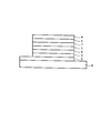
- FIG. 1 is a schematic cross-sectional view showing an embodiment of an organic EL device.
- the organic EL device shown in FIG. 1 is a multi-layered device, and has a substrate 8, an anode 2, a hole injection layer 3, a hole transport layer 6, a light emitting layer 1, an electron transport layer 7, an electron injection layer 5, and a cathode. It has a multi-layer structure in which 4 are laminated in this order.
- FIG. 1 is an example, and the organic EL element of the present embodiment is not limited to this figure.
- the hole injection layer 3 is an organic layer formed by using the above-mentioned organic electronic material, but the organic EL device of the present embodiment is not limited to such a structure, and other organic layers may be used.
- It may be an organic layer formed by using the above-mentioned organic electronic material.
- a hole transport layer a hole transport layer
- a hole injection layer a hole injection layer
- a light emitting layer a layer selected from the group consisting of a hole transport layer, a hole injection layer and a light emitting layer.
- Light emitting layer As the material used for the light emitting layer, a light emitting material such as a low molecular weight compound, a polymer, or a dendrimer can be used. Polymers are preferred because they are highly soluble in solvents and suitable for coating methods. Examples of the light emitting material include fluorescent materials, phosphorescent materials, thermal activated delayed fluorescent materials (TADF) and the like.
- TADF thermal activated delayed fluorescent materials
- Low molecular weight compounds such as perylene, coumarin, rubrene, quinacridone, stilbene, dyes for dye lasers, aluminum complexes, and derivatives thereof as fluorescent materials; polyfluorene, polyphenylene, polyphenylene vinylene, polyvinylcarbazole, fluorene-benzothiazol copolymer , Fluorene-triphenylamine copolymers, polymers such as derivatives thereof; mixtures thereof and the like.
- a metal complex containing a metal such as Ir or Pt can be used.
- Ir complex include FIr (pic) (iridium (III) bis [(4,6-difluorophenyl) -pyridinate-N, C 2 ] picolinate) that emits blue light, and Ir (ppy) 3 that emits green light.
- the light emitting layer contains a phosphorescent material
- a host material a low molecular weight compound, a polymer, or a dendrimer can be used.
- low molecular weight compounds include CBP (4,4'-bis (9H-carbazole-9-yl) biphenyl), mCP (1,3-bis (9-carbazolyl) benzene), and CDBP (4,4'-.
- thermally activated delayed fluorescent materials include Adv. Mater., 21, 4802-4906 (2009); Appl. Phys. Lett., 98, 083302 (2011); Chem. Comm., 48, 9580 (2012). Appl. Phys. Lett., 101, 093306 (2012); J. Am. Chem. Soc., 134, 14706 (2012); Chem. Comm., 48, 11392 (2012); Nature, 492, 234 (2012) ); Adv. Mater., 25, 3319 (2013); J. Phys. Chem. A, 117, 5607 (2013); Phys. Chem. Chem. Phys., 15, 15850 (2013); Chem. Comm., 49, 10385 (2013); Chem. Lett., 43, 319 (2014), etc. can be used.
- the above-mentioned organic layer is preferably used as at least one of the hole injection layer and the hole transport layer, and more preferably at least as the hole transport layer.
- a known material can be used for the hole injection layer.
- a known material can be used for the hole transport layer.
- Examples of materials that can be used for the hole injection layer and the hole transport layer include aromatic amine compounds, phthalocyanine compounds, and thiophene compounds.
- Electrode transport layer electron injection layer
- Examples of the material used for the electron transport layer and the electron injection layer include fused ring tetracarboxylic acid anhydrides such as phenanthroline derivative, bipyridine derivative, nitro-substituted fluorene derivative, diphenylquinone derivative, thiopyrandioxide derivative, naphthalene and perylene, and carbodiimide. , Fluolenilidene methane derivative, anthraquinodimethane and antron derivative, oxadiazole derivative, thiadiazole derivative, benzoimidazole derivative, quinoxalin derivative, aluminum complex (for example, BAlq, Alq 3 ) and the like. Further, the organic electronic material of the above-described embodiment can also be used.
- cathode As the cathode material, for example, a metal or a metal alloy such as Li, Ca, Mg, Al, In, Cs, Ba, Mg / Ag, LiF, CsF is used.
- a metal or a metal alloy such as Li, Ca, Mg, Al, In, Cs, Ba, Mg / Ag, LiF, CsF is used.
- anode for example, a metal (for example, Au) or another conductive material is used.
- Other materials include, for example, oxides (eg, ITO), conductive polymers (eg, polythiophene-polystyrene sulfonic acid mixture (PEDOT: PSS)).
- [substrate] Glass, plastic, etc. can be used as the substrate.
- the substrate is preferably transparent and preferably has flexibility. Quartz glass, light-transmitting resin film and the like are preferably used.
- the resin film for example, a film containing polyethylene terephthalate, polyethylene naphthalate, polyether sulfone, polyetherimide, polyetheretherketone, polyphenylene sulfide, polyarylate, polyimide, polycarbonate, cellulose triacetate, cellulose acetate propionate and the like. Can be mentioned.
- the resin film When a resin film is used, the resin film may be coated with an inorganic substance such as silicon oxide or silicon nitride in order to suppress the permeation of water vapor, oxygen, etc.
- an inorganic substance such as silicon oxide or silicon nitride
- the emission color of the organic EL element is not particularly limited.
- An organic EL element exhibiting white light emission (also referred to as a white organic EL element) is preferable because it can be used for various lighting fixtures such as household lighting, vehicle interior lighting, clocks, and liquid crystal backlights.
- a method for forming the white organic EL element a method of simultaneously emitting a plurality of emission colors using a plurality of light emitting materials and mixing the colors can be used.
- the combination of a plurality of emission colors is not particularly limited, but for example, a combination containing three emission maximum wavelengths of blue, green and red, and a complementary color relationship such as blue and yellow and yellow-green and orange. Examples thereof include a combination containing the two maximum emission wavelengths used.
- the emission color can be controlled by adjusting the type and amount of the emission material.
- the display element of the present embodiment includes the organic EL element of the above-described embodiment.
- an organic EL element as an element corresponding to each pixel of red, green, and blue (RGB)
- RGB red, green, and blue
- the lighting device of the present embodiment includes the organic EL element of the above-described embodiment.
- the display device of the present embodiment includes a lighting device and a liquid crystal element as a display means.
- the display device can be a display device using the lighting device of the above-described embodiment as a backlight and a known liquid crystal element as a display means, that is, a liquid crystal display device.
- Example 1 (Synthesis of Ionic Compound 1) Ionic compound 1 having the following structure was synthesized as follows. 25 g of acetone and 5 g of pure water were added to 1.111 g (10 mmol) of diallyl methylamine and stirred to obtain a uniform solution, and then 3.653 g of a 10% hydrogen chloride aqueous solution was slowly added dropwise, and the mixture was stirred for 1 hour after the completion of the addition. The solvent was distilled off from this solution under reduced pressure. Then, 77.49 g (11 mmol) of a 10% aqueous solution of Sodium tetrakis (pentafluorophenyl) borate was mixed, and the mixture was stirred for 1 hour. This was washed with water 5 times and dried to prepare a white solid.
- Example 2 (Synthesis of Ionic Compound 2) Ionic compound 2 having the following structure was synthesized as follows. To 1.132 g (10 mmol) of diethylallylamine, 25 g of acetone and 5 g of pure water were added and stirred to obtain a uniform solution, and then 3.653 g of a 10% hydrogen chloride aqueous solution was slowly added dropwise, and the mixture was stirred for 1 hour after the completion of the addition. The solvent was distilled off from this solution under reduced pressure. Then, 77.49 g (11 mmol) of a 10% aqueous solution of Sodium tetrakis (pentafluorophenyl) borate was mixed, and the mixture was stirred for 1 hour. This was washed with water 5 times and dried to prepare a white solid.
- Example 3 (Synthesis of Ionic Compound 3)
- the ionic compound 3 having the following structure was synthesized as follows. To 1.372 g (10 mmol) of triallylamine, 25 g of acetone and 5 g of pure water were added and stirred to obtain a uniform solution, and then 3.653 g of a 10% hydrogen chloride aqueous solution was slowly added dropwise, and the mixture was stirred for 1 hour after the completion of the addition. The solvent was distilled off from this solution under reduced pressure. Then, 77.49 g (11 mmol) of a 10% aqueous solution of Sodium tetrakis (pentafluorophenyl) borate was mixed, and the mixture was stirred for 1 hour. This was washed with water 5 times and dried to prepare a white solid.
- thermogravimetric reduction was determined by measuring 10 mg of each of the produced ionic compounds in air using a TG-DTA measuring device (DTG-60H manufactured by Shimadzu Corporation) under a temperature rising condition of 5 ° C./min.
- the temperature at which the weight loss of 2% occurred when each ionic compound was heated was defined as the weight loss temperature.
- Table 1 shows the evaluation results of the weight loss temperature.
- the ionic compounds 1 to 3 (Examples 1 to 3) in the above-described embodiment showed higher weight loss temperatures than the ionic compounds 4 to 7 (Comparative Examples 1 to 4). It can be seen that the heat resistance is excellent by using an ionic compound having a small thermal weight loss.
- a charge-transporting polymer 1 was prepared as shown below. The monomers used are shown below.
- the charge-transporting polymer 1 had a number average molecular weight of 11,900 and a weight average molecular weight of 66,200.
- the number average molecular weight and the weight average molecular weight were measured by GPC (polystyrene conversion) using tetrahydrofuran (THF) as an eluent.
- the measurement conditions are as follows.
- Organic layers A1 to 7 were formed using the charge-transporting polymer 1 and the ionic compounds 1 to 7, and the solvent resistance was evaluated by measuring the residual film ratio.
- Example 1 The ionic compound (10 mg) used in Example 1 was weighed into a 20 mL screw tube, a certain amount of chlorobenzene was added, and the mixture was stirred to prepare an ionic compound solution. Then, the charge-transporting polymer 1 (10 mg) and a certain amount of chlorobenzene (792 ⁇ L) were added to the 9 mL screw tube to dissolve the charge-transporting polymer. Then, a certain amount of the ionic compound solution was added to the above-mentioned 9 mL screw tube and stirred to prepare an ink composition.
- the ink composition is filtered through a polytetrafluoroethylene (PTFE) filter (pore diameter 0.2 ⁇ m), dropped onto a quartz substrate (length 22 mm ⁇ width 29 mm ⁇ thickness 0.7 mm), and a coating film is formed by a spin coater. Membrane. Subsequently, heat curing was carried out at 200 ° C. for 30 minutes in a nitrogen atmosphere to form an organic layer having a film thickness of 30 nm on a quartz substrate. (The solution was adjusted so that the charge-transporting polymer was 1 wt% and the ionic compound was 1 wt% with respect to the charge-transporting polymer.)
- PTFE polytetrafluoroethylene
- the absorbance A of the organic layer formed on the quartz substrate was measured using a spectrophotometer (“UV-2700” manufactured by Shimadzu Corporation). Subsequently, the mixture was immersed in anisole (10 mL, 25 ° C.) for 10 minutes in an environment of 25 ° C. so that the organic layer after measurement was on the upper surface.
- the absorbance B of the organic layer after immersion in anisole was measured, and the residual film ratio was calculated from the absorbance A of the formed organic layer and the absorbance B of the organic layer after immersion in anisole using the following formula.
- the value of absorbance the value at the maximum absorption wavelength of the organic layer was used. The larger the residual film ratio, the better the solvent resistance.
- Table 2 shows the measurement results of the residual film ratio.
- the organic layers A1 to A3 using the ionic compounds 1 to 3 of the present embodiment have a better residual film ratio and a film forming property as compared with the organic layers A4 to A7 using the ionic compounds 4 to 7. Good measurement results were shown.
- Organic EL devices 1 to 7 were prepared using the charge-transporting polymer 1 and the ionic compounds 1 to 7 according to the following, and the drive voltage, luminous efficiency, and emission lifetime were evaluated.
- Example 2 Manufacturing of organic EL element
- the ionic compound (10.0 mg) used in Example 1 was weighed into a 20 mL screw tube, a certain amount of chlorobenzene was added, and the mixture was stirred to prepare an ionic compound solution.
- a charge-transporting polymer (10 mg) and a certain amount of chlorobenzene were added to the 9 mL screw tube to dissolve the charge-transporting polymer.
- a certain amount of the ionic compound solution was added to the above-mentioned 9 mL screw tube and stirred to prepare an ink composition.
- a patterned ITO having a width of 1.6 mm is formed on a glass substrate (length 22 mm ⁇ width 29 mm ⁇ thickness 0.7 mm), and an ink composition is applied onto the glass substrate and the formed ITO with a polytetrafluoroethylene (PTFE) filter (PTFE).
- PTFE polytetrafluoroethylene
- the filtrate prepared by filtering with a pore size of 0.2 ⁇ m) was dropped, and a coating film was formed by a spin coater. Then, it was heated on a hot plate at 200 ° C. for 30 minutes in a nitrogen atmosphere to form a hole injection layer (30 nm).
- the solution was adjusted so that the charge-transporting polymer was 1 wt% and the ionic compound was 1 wt% with respect to the charge-transporting polymer.
- the glass substrate having the hole injection layer is transferred into the vacuum vapor deposition machine, and ⁇ -NPD (40 nm), CBP: Ir (ppy) 3 (94: 6, 30 nm), BAlq (10 nm), TPBi are placed on the hole injection layer. (30 nm), LiF (0.8 nm), and Al (100 nm) were deposited in this order by a vapor deposition method. Then, a sealing process was performed to produce an organic EL element.
- Table 3 shows the measurement results of drive voltage, luminous efficiency, and luminous life.
- the organic EL devices 1 to 3 using the ionic compounds 1 to 3 of the present embodiment are compared with the organic EL devices 4 to 7 using the ionic compounds 4 to 7 in terms of drive voltage, light emission efficiency, and light emission lifetime. Good measurement results were shown.
Landscapes
- Chemical & Material Sciences (AREA)
- Organic Chemistry (AREA)
- Physics & Mathematics (AREA)
- Optics & Photonics (AREA)
- Electroluminescent Light Sources (AREA)
- Organic Low-Molecular-Weight Compounds And Preparation Thereof (AREA)
- Liquid Crystal (AREA)
- Polyoxymethylene Polymers And Polymers With Carbon-To-Carbon Bonds (AREA)
Priority Applications (3)
| Application Number | Priority Date | Filing Date | Title |
|---|---|---|---|
| JP2021543806A JP7444170B2 (ja) | 2019-09-02 | 2019-09-02 | イオン性化合物、有機エレクトロニクス材料、有機層、有機エレクトロニクス素子、有機エレクトロルミネセンス素子、表示素子、照明装置、及び有機エレクトロニクス素子の製造方法 |
| PCT/JP2019/034408 WO2021044478A1 (ja) | 2019-09-02 | 2019-09-02 | イオン性化合物、有機エレクトロニクス材料、有機層、有機エレクトロニクス素子、有機エレクトロルミネセンス素子、表示素子、照明装置、及び有機エレクトロニクス素子の製造方法 |
| JP2023213579A JP2024037956A (ja) | 2019-09-02 | 2023-12-19 | イオン性化合物、有機エレクトロニクス材料、有機層、有機エレクトロニクス素子、有機エレクトロルミネセンス素子、表示素子、照明装置、及び有機エレクトロニクス素子の製造方法 |
Applications Claiming Priority (1)
| Application Number | Priority Date | Filing Date | Title |
|---|---|---|---|
| PCT/JP2019/034408 WO2021044478A1 (ja) | 2019-09-02 | 2019-09-02 | イオン性化合物、有機エレクトロニクス材料、有機層、有機エレクトロニクス素子、有機エレクトロルミネセンス素子、表示素子、照明装置、及び有機エレクトロニクス素子の製造方法 |
Publications (1)
| Publication Number | Publication Date |
|---|---|
| WO2021044478A1 true WO2021044478A1 (ja) | 2021-03-11 |
Family
ID=74852532
Family Applications (1)
| Application Number | Title | Priority Date | Filing Date |
|---|---|---|---|
| PCT/JP2019/034408 Ceased WO2021044478A1 (ja) | 2019-09-02 | 2019-09-02 | イオン性化合物、有機エレクトロニクス材料、有機層、有機エレクトロニクス素子、有機エレクトロルミネセンス素子、表示素子、照明装置、及び有機エレクトロニクス素子の製造方法 |
Country Status (2)
| Country | Link |
|---|---|
| JP (2) | JP7444170B2 (https=) |
| WO (1) | WO2021044478A1 (https=) |
Cited By (3)
| Publication number | Priority date | Publication date | Assignee | Title |
|---|---|---|---|---|
| WO2023039514A1 (en) * | 2021-09-10 | 2023-03-16 | Dow Global Technologies Llc | Hydrocarbon soluble borate cocatalysts for olefin polymerization |
| WO2025013809A1 (ja) * | 2023-07-10 | 2025-01-16 | 株式会社レゾナック | 有機エレクトロニクス材料、有機層、有機エレクトロニクス素子、表示素子、照明装置、及び表示装置 |
| WO2025013808A1 (ja) * | 2023-07-10 | 2025-01-16 | 株式会社レゾナック | 有機エレクトロニクス材料、有機層、有機エレクトロニクス素子 |
Citations (3)
| Publication number | Priority date | Publication date | Assignee | Title |
|---|---|---|---|---|
| JP2007510002A (ja) * | 2003-11-05 | 2007-04-19 | ノバルティス アクチエンゲゼルシャフト | 大環状ラクタムおよびその医薬的使用 |
| WO2010140553A1 (ja) * | 2009-06-01 | 2010-12-09 | 日立化成工業株式会社 | 有機エレクトロニクス材料およびそれを含むインク組成物、ならびにそれらを用いて形成された有機薄膜、有機エレクトロニクス素子、有機エレクトロルミネセンス素子、照明装置および表示装置 |
| CN109369413A (zh) * | 2018-10-29 | 2019-02-22 | 邹平铭兴化工有限公司 | 二烯丙基胺及其盐酸盐的制备方法 |
Family Cites Families (1)
| Publication number | Priority date | Publication date | Assignee | Title |
|---|---|---|---|---|
| CN109269413A (zh) | 2018-11-28 | 2019-01-25 | 信利光电股份有限公司 | 基于飞行时间法测量物件尺寸的设备 |
-
2019
- 2019-09-02 JP JP2021543806A patent/JP7444170B2/ja active Active
- 2019-09-02 WO PCT/JP2019/034408 patent/WO2021044478A1/ja not_active Ceased
-
2023
- 2023-12-19 JP JP2023213579A patent/JP2024037956A/ja active Pending
Patent Citations (3)
| Publication number | Priority date | Publication date | Assignee | Title |
|---|---|---|---|---|
| JP2007510002A (ja) * | 2003-11-05 | 2007-04-19 | ノバルティス アクチエンゲゼルシャフト | 大環状ラクタムおよびその医薬的使用 |
| WO2010140553A1 (ja) * | 2009-06-01 | 2010-12-09 | 日立化成工業株式会社 | 有機エレクトロニクス材料およびそれを含むインク組成物、ならびにそれらを用いて形成された有機薄膜、有機エレクトロニクス素子、有機エレクトロルミネセンス素子、照明装置および表示装置 |
| CN109369413A (zh) * | 2018-10-29 | 2019-02-22 | 邹平铭兴化工有限公司 | 二烯丙基胺及其盐酸盐的制备方法 |
Non-Patent Citations (2)
| Title |
|---|
| D'ARCY, R. ET AL.: "Die synchrone Fragmentierung von γ-Amino-cycloalkylhalogeniden. 3. Teil. 4-Chlorpiperidine Fragmentierungsrcaktionen, 13. Mitteilung", HELVETICA CHIMICA ACTA, vol. 49, no. 1, 1966, pages 185 - 203, XP055803267 * |
| PAVLOV, GEORGES M. ET AL.: "Strong Linear Polyelectrolytes in Solutions of Extreme Concentrations of One–One Valent Salt. Hydrodynamic Study", MACROMOLECULES, vol. 47, 3 April 2014 (2014-04-03), pages 2748 - 2758, XP055803260 * |
Cited By (3)
| Publication number | Priority date | Publication date | Assignee | Title |
|---|---|---|---|---|
| WO2023039514A1 (en) * | 2021-09-10 | 2023-03-16 | Dow Global Technologies Llc | Hydrocarbon soluble borate cocatalysts for olefin polymerization |
| WO2025013809A1 (ja) * | 2023-07-10 | 2025-01-16 | 株式会社レゾナック | 有機エレクトロニクス材料、有機層、有機エレクトロニクス素子、表示素子、照明装置、及び表示装置 |
| WO2025013808A1 (ja) * | 2023-07-10 | 2025-01-16 | 株式会社レゾナック | 有機エレクトロニクス材料、有機層、有機エレクトロニクス素子 |
Also Published As
| Publication number | Publication date |
|---|---|
| JPWO2021044478A1 (https=) | 2021-03-11 |
| JP7444170B2 (ja) | 2024-03-06 |
| JP2024037956A (ja) | 2024-03-19 |
Similar Documents
| Publication | Publication Date | Title |
|---|---|---|
| JP7044063B2 (ja) | 有機エレクトロニクス材料及びその利用 | |
| JP2024037956A (ja) | イオン性化合物、有機エレクトロニクス材料、有機層、有機エレクトロニクス素子、有機エレクトロルミネセンス素子、表示素子、照明装置、及び有機エレクトロニクス素子の製造方法 | |
| JP6782418B2 (ja) | 有機エレクトロニクス材料及びその利用 | |
| WO2018143438A1 (ja) | 有機エレクトロニクス材料及びその利用 | |
| JP7103424B2 (ja) | 有機エレクトロニクス材料及びその利用 | |
| JP7363214B2 (ja) | イオン性化合物、有機エレクトロニクス材料、インク組成物、及び有機エレクトロニクス素子 | |
| JP6641845B2 (ja) | 電荷輸送性材料、該材料を用いたインキ組成物、有機エレクトロニクス素子、有機エレクトロルミネセンス素子、表示素子、照明装置、及び表示装置 | |
| JP2022016775A (ja) | 有機エレクトロニクス材料、インク組成物、有機層、有機エレクトロニクス素子、有機エレクトロルミネセンス素子、照明装置、表示素子、及び表示装置 | |
| JP6954284B2 (ja) | 有機エレクトロニクス材料 | |
| JPWO2020090294A1 (ja) | イオン性化合物、有機エレクトロニクス材料、インク組成物、及び有機エレクトロニクス素子 | |
| JPWO2020067300A1 (ja) | 有機エレクトロニクス材料及び有機エレクトロニクス素子 | |
| JP6775736B2 (ja) | 電荷輸送性材料、該材料を用いたインク組成物、有機エレクトロニクス素子、有機エレクトロルミネセンス素子、表示素子、照明装置、及び表示装置 | |
| JP6775731B2 (ja) | 電荷輸送性材料及びその利用 | |
| JP6769020B2 (ja) | 電荷輸送性材料、該材料を用いたインク組成物、有機エレクトロニクス素子、有機エレクトロルミネセンス素子、表示素子、照明装置、及び表示装置 | |
| JP6946934B2 (ja) | 電荷輸送性材料及び有機エレクトロニクス素子 | |
| JP6972589B2 (ja) | 有機エレクトロニクス材料、及び該材料を用いた有機層、有機エレクトロニクス素子、有機エレクトロルミネセンス素子、表示素子、照明装置、及び表示装置 | |
| JP2020145234A (ja) | 有機エレクトロニクス材料及びその利用 | |
| JPWO2020065920A1 (ja) | 有機エレクトロニクス材料及び有機エレクトロニクス素子 | |
| JP6816540B2 (ja) | 電荷輸送性材料、該材料を用いたインク組成物、有機エレクトロニクス素子、有機エレクトロルミネセンス素子、表示素子、照明装置、及び表示装置 | |
| WO2019009327A1 (ja) | 有機エレクトロニクス材料及び有機エレクトロニクス素子 | |
| JP2017218426A (ja) | イオン性化合物、有機エレクトロニクス材料、有機エレクトロニクス素子、及び有機エレクトロルミネセンス素子 | |
| JP2019131670A (ja) | 有機エレクトロニクス材料 | |
| JP6756143B2 (ja) | 有機エレクトロニクス材料及び有機エレクトロルミネセンス素子 | |
| JP6657663B2 (ja) | 電荷輸送性材料、該材料を用いたインク組成物、有機エレクトロニクス素子、有機エレクトロルミネセンス素子、表示素子、表示装置及び照明装置 | |
| JP6915621B2 (ja) | 電荷輸送性材料、インク組成物、及び有機エレクトロニクス素子 |
Legal Events
| Date | Code | Title | Description |
|---|---|---|---|
| 121 | Ep: the epo has been informed by wipo that ep was designated in this application |
Ref document number: 19944298 Country of ref document: EP Kind code of ref document: A1 |
|
| WWE | Wipo information: entry into national phase |
Ref document number: 2021543806 Country of ref document: JP |
|
| NENP | Non-entry into the national phase |
Ref country code: DE |
|
| 32PN | Ep: public notification in the ep bulletin as address of the adressee cannot be established |
Free format text: NOTING OF LOSS OF RIGHTS PURSUANT TO RULE 112(1) EPC (EPO FORM 1205A DATED 07/06/2022) |
|
| 122 | Ep: pct application non-entry in european phase |
Ref document number: 19944298 Country of ref document: EP Kind code of ref document: A1 |