WO2021024997A1 - 半導体光増幅器アレイ素子 - Google Patents
半導体光増幅器アレイ素子 Download PDFInfo
- Publication number
- WO2021024997A1 WO2021024997A1 PCT/JP2020/029723 JP2020029723W WO2021024997A1 WO 2021024997 A1 WO2021024997 A1 WO 2021024997A1 JP 2020029723 W JP2020029723 W JP 2020029723W WO 2021024997 A1 WO2021024997 A1 WO 2021024997A1
- Authority
- WO
- WIPO (PCT)
- Prior art keywords
- semiconductor optical
- optical amplifier
- semiconductor
- array element
- input
- Prior art date
- Legal status (The legal status is an assumption and is not a legal conclusion. Google has not performed a legal analysis and makes no representation as to the accuracy of the status listed.)
- Ceased
Links
Images
Classifications
-
- H—ELECTRICITY
- H01—ELECTRIC ELEMENTS
- H01S—DEVICES USING THE PROCESS OF LIGHT AMPLIFICATION BY STIMULATED EMISSION OF RADIATION [LASER] TO AMPLIFY OR GENERATE LIGHT; DEVICES USING STIMULATED EMISSION OF ELECTROMAGNETIC RADIATION IN WAVE RANGES OTHER THAN OPTICAL
- H01S5/00—Semiconductor lasers
- H01S5/50—Amplifier structures not provided for in groups H01S5/02 - H01S5/30
- H01S5/5009—Amplifier structures not provided for in groups H01S5/02 - H01S5/30 the arrangement being polarisation-insensitive
- H01S5/5018—Amplifier structures not provided for in groups H01S5/02 - H01S5/30 the arrangement being polarisation-insensitive using two or more amplifiers or multiple passes through the same amplifier
-
- H—ELECTRICITY
- H01—ELECTRIC ELEMENTS
- H01S—DEVICES USING THE PROCESS OF LIGHT AMPLIFICATION BY STIMULATED EMISSION OF RADIATION [LASER] TO AMPLIFY OR GENERATE LIGHT; DEVICES USING STIMULATED EMISSION OF ELECTROMAGNETIC RADIATION IN WAVE RANGES OTHER THAN OPTICAL
- H01S5/00—Semiconductor lasers
- H01S5/50—Amplifier structures not provided for in groups H01S5/02 - H01S5/30
-
- H—ELECTRICITY
- H01—ELECTRIC ELEMENTS
- H01S—DEVICES USING THE PROCESS OF LIGHT AMPLIFICATION BY STIMULATED EMISSION OF RADIATION [LASER] TO AMPLIFY OR GENERATE LIGHT; DEVICES USING STIMULATED EMISSION OF ELECTROMAGNETIC RADIATION IN WAVE RANGES OTHER THAN OPTICAL
- H01S5/00—Semiconductor lasers
- H01S5/02—Structural details or components not essential to laser action
- H01S5/022—Mountings; Housings
- H01S5/0225—Out-coupling of light
-
- H—ELECTRICITY
- H01—ELECTRIC ELEMENTS
- H01S—DEVICES USING THE PROCESS OF LIGHT AMPLIFICATION BY STIMULATED EMISSION OF RADIATION [LASER] TO AMPLIFY OR GENERATE LIGHT; DEVICES USING STIMULATED EMISSION OF ELECTROMAGNETIC RADIATION IN WAVE RANGES OTHER THAN OPTICAL
- H01S5/00—Semiconductor lasers
- H01S5/02—Structural details or components not essential to laser action
- H01S5/026—Monolithically integrated components, e.g. waveguides, monitoring photo-detectors, drivers
-
- H—ELECTRICITY
- H01—ELECTRIC ELEMENTS
- H01S—DEVICES USING THE PROCESS OF LIGHT AMPLIFICATION BY STIMULATED EMISSION OF RADIATION [LASER] TO AMPLIFY OR GENERATE LIGHT; DEVICES USING STIMULATED EMISSION OF ELECTROMAGNETIC RADIATION IN WAVE RANGES OTHER THAN OPTICAL
- H01S5/00—Semiconductor lasers
- H01S5/10—Construction or shape of the optical resonator, e.g. extended or external cavity, coupled cavities, bent-guide, varying width, thickness or composition of the active region
- H01S5/1053—Comprising an active region having a varying composition or cross-section in a specific direction
- H01S5/1057—Comprising an active region having a varying composition or cross-section in a specific direction varying composition along the optical axis
-
- H—ELECTRICITY
- H01—ELECTRIC ELEMENTS
- H01S—DEVICES USING THE PROCESS OF LIGHT AMPLIFICATION BY STIMULATED EMISSION OF RADIATION [LASER] TO AMPLIFY OR GENERATE LIGHT; DEVICES USING STIMULATED EMISSION OF ELECTROMAGNETIC RADIATION IN WAVE RANGES OTHER THAN OPTICAL
- H01S5/00—Semiconductor lasers
- H01S5/10—Construction or shape of the optical resonator, e.g. extended or external cavity, coupled cavities, bent-guide, varying width, thickness or composition of the active region
- H01S5/1082—Construction or shape of the optical resonator, e.g. extended or external cavity, coupled cavities, bent-guide, varying width, thickness or composition of the active region with a special facet structure, e.g. structured, non planar, oblique
- H01S5/1085—Oblique facets
-
- H—ELECTRICITY
- H01—ELECTRIC ELEMENTS
- H01S—DEVICES USING THE PROCESS OF LIGHT AMPLIFICATION BY STIMULATED EMISSION OF RADIATION [LASER] TO AMPLIFY OR GENERATE LIGHT; DEVICES USING STIMULATED EMISSION OF ELECTROMAGNETIC RADIATION IN WAVE RANGES OTHER THAN OPTICAL
- H01S5/00—Semiconductor lasers
- H01S5/10—Construction or shape of the optical resonator, e.g. extended or external cavity, coupled cavities, bent-guide, varying width, thickness or composition of the active region
- H01S5/1003—Waveguide having a modified shape along the axis, e.g. branched, curved, tapered, voids
- H01S5/101—Curved waveguide
-
- H—ELECTRICITY
- H01—ELECTRIC ELEMENTS
- H01S—DEVICES USING THE PROCESS OF LIGHT AMPLIFICATION BY STIMULATED EMISSION OF RADIATION [LASER] TO AMPLIFY OR GENERATE LIGHT; DEVICES USING STIMULATED EMISSION OF ELECTROMAGNETIC RADIATION IN WAVE RANGES OTHER THAN OPTICAL
- H01S5/00—Semiconductor lasers
- H01S5/20—Structure or shape of the semiconductor body to guide the optical wave ; Confining structures perpendicular to the optical axis, e.g. index or gain guiding, stripe geometry, broad area lasers, gain tailoring, transverse or lateral reflectors, special cladding structures, MQW barrier reflection layers
- H01S5/22—Structure or shape of the semiconductor body to guide the optical wave ; Confining structures perpendicular to the optical axis, e.g. index or gain guiding, stripe geometry, broad area lasers, gain tailoring, transverse or lateral reflectors, special cladding structures, MQW barrier reflection layers having a ridge or stripe structure
- H01S5/227—Buried mesa structure ; Striped active layer
-
- H—ELECTRICITY
- H01—ELECTRIC ELEMENTS
- H01S—DEVICES USING THE PROCESS OF LIGHT AMPLIFICATION BY STIMULATED EMISSION OF RADIATION [LASER] TO AMPLIFY OR GENERATE LIGHT; DEVICES USING STIMULATED EMISSION OF ELECTROMAGNETIC RADIATION IN WAVE RANGES OTHER THAN OPTICAL
- H01S5/00—Semiconductor lasers
- H01S5/30—Structure or shape of the active region; Materials used for the active region
- H01S5/34—Structure or shape of the active region; Materials used for the active region comprising quantum well or superlattice structures, e.g. single quantum well [SQW] lasers, multiple quantum well [MQW] lasers or graded index separate confinement heterostructure [GRINSCH] lasers
- H01S5/343—Structure or shape of the active region; Materials used for the active region comprising quantum well or superlattice structures, e.g. single quantum well [SQW] lasers, multiple quantum well [MQW] lasers or graded index separate confinement heterostructure [GRINSCH] lasers in AIIIBV compounds, e.g. AlGaAs-laser, InP-based laser
- H01S5/34306—Structure or shape of the active region; Materials used for the active region comprising quantum well or superlattice structures, e.g. single quantum well [SQW] lasers, multiple quantum well [MQW] lasers or graded index separate confinement heterostructure [GRINSCH] lasers in AIIIBV compounds, e.g. AlGaAs-laser, InP-based laser emitting light at a wavelength longer than 1000nm, e.g. InP based 1300 and 1500nm lasers
-
- H—ELECTRICITY
- H01—ELECTRIC ELEMENTS
- H01S—DEVICES USING THE PROCESS OF LIGHT AMPLIFICATION BY STIMULATED EMISSION OF RADIATION [LASER] TO AMPLIFY OR GENERATE LIGHT; DEVICES USING STIMULATED EMISSION OF ELECTROMAGNETIC RADIATION IN WAVE RANGES OTHER THAN OPTICAL
- H01S5/00—Semiconductor lasers
- H01S5/40—Arrangement of two or more semiconductor lasers, not provided for in groups H01S5/02 - H01S5/30
- H01S5/4025—Array arrangements, e.g. constituted by discrete laser diodes or laser bar
Definitions
- the present invention relates to a semiconductor optical amplifier array element.
- Digital coherent communication using the digital coherent method is widely applied in optical communication systems.
- Digital coherent communication has been used for long distances (long holes). In recent years, the applicable distance has become shorter, and the digital coherent method has come to be used between metro systems and data centers.
- InP modulators using InP-based semiconductor materials and modulators using Si photonics have come to be used as modulators in transmitters of digital coherent communication systems. I came.
- the InP modulator often has an integrated semiconductor optical amplifier (SOA) as in Non-Patent Document 1.
- SOA semiconductor optical amplifier
- the modulator has four semiconductor optical amplifiers. Two of them are "Pre-semiconductor optical amplifiers” that amplify the input continuous light, and the other two are “Post-semiconductor optical amplifiers” that amplify the modulated light.
- Patent Document 1 discloses a semiconductor optical amplifier having a U-turn structure as a semiconductor optical amplifier for hybrid integration.
- a semiconductor optical amplifier having a U-turn structure has an input port for inputting amplified light and an output port for outputting amplified light on the same end face, and further has a bent waveguide that turns back an optical path.
- the present invention has been made in view of the above, and an object of the present invention is to provide a semiconductor optical amplifier array element in which semiconductor optical amplifiers having different characteristics are integrated.
- one aspect of the present invention includes a substrate and a plurality of semiconductor optical amplifiers formed on the substrate and each having an active region.
- the two optical input / output ports of the plurality of semiconductor optical amplifiers are each optically connected to each of the active regions, and both are provided on the same end face of the semiconductor optical amplifier array element.
- the plurality of semiconductor optical amplifiers include a first semiconductor optical amplifier in which the length of the active region is the first length, and a second semiconductor optical amplifier having a second length in which the length of the active region is different from the first length.
- a semiconductor optical amplifier array element including an amplifier.
- the plurality of semiconductor optical amplifiers may have a folding portion formed between the two optical input / output ports by a waveguide in which the optical path is folded back at an angle of substantially 180 degrees.
- the first length of the first semiconductor optical amplifier is longer than the second length of the second semiconductor optical amplifier, and continuous light is input to the optical input / output port of the first semiconductor optical amplifier, and the second Modulated light may be input to the optical input / output port of the semiconductor optical amplifier.
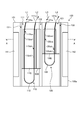
- FIG. 1 is a schematic plan view of the semiconductor optical amplifier array element according to the first embodiment.
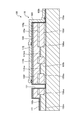
- FIG. 2 is a schematic partial cross-sectional view of the semiconductor optical amplifier array element shown in FIG.
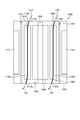
- FIG. 3 is a schematic plan view of the semiconductor optical amplifier array element according to the reference embodiment.
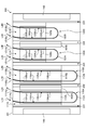
- FIG. 4 is a schematic plan view of the semiconductor optical amplifier array element according to the second embodiment.
- FIG. 5 is a schematic configuration diagram of the optical module according to the third embodiment.
- FIG. 1 is a schematic plan view of the semiconductor optical amplifier array element according to the first embodiment.
- the chip-shaped semiconductor optical amplifier array element 100 includes semiconductor optical amplifiers 110 and 120 as a plurality of semiconductor optical amplifiers.
- the semiconductor optical amplifiers 110 and 120 are formed on the substrate 100a and are integrated on one substrate 100a.
- the semiconductor optical amplifier 110 is an example of a first semiconductor optical amplifier
- the semiconductor optical amplifier 120 is an example of a second semiconductor optical amplifier.
- the semiconductor optical amplifier array element 100 is mainly composed of a group III-V semiconductor material.
- the semiconductor optical amplifier 110 includes an active unit 111 and a passive unit 112.
- the active portion 111 has an embedded waveguide structure suitable for a current injection type light emitting element, and has active layers 110ca and 110 cab as optical waveguides.
- the passive portion 112 is bent in a U shape and has a high-mesa waveguide structure including an optical waveguide as a passive waveguide.
- the high mesa waveguide structure is also called a deep ridge waveguide structure.
- the passive portion 112 is an example of a folded portion composed of a waveguide in which the optical path is folded back at an angle of substantially 180 degrees.
- the active layers 110ca and 110cc have a multiple quantum well (MQW) structure made of, for example, a GaInAsP-based semiconductor material or an AlGaInAs-based semiconductor material.
- the clad layer is made of n-type InP or i-type InP
- the optical waveguide is made of, for example, an i-type GaInAsP-based semiconductor material having a bandgap wavelength of 1300 nm.
- the active layers 110ca and 110cc and the optical waveguide of the passive portion 112 are optically connected by a butt joint connection or the like.
- the active layer 110ca and the active layer 110cc are substantially parallel to each other, and are optically connected via an optical waveguide having a high-mesa waveguide structure of the passive portion 112.
- the semiconductor optical amplifier 110 includes a power feeding unit 110j.
- the semiconductor optical amplifier 110 has optical input / output ports 111a and 111b provided on the end surface 101, which is one end surface of the semiconductor optical amplifier array element 100.
- the optical input / output ports 111a and 111b are connected to the active layers 110ca and 110cc, respectively.
- the active layers 110ca and 110cc are inclined with respect to the normal line of the end face 101 on the end face 101 side.
- the semiconductor optical amplifier 120 includes an active unit 121 and a passive unit 122.
- the active portion 121 has an embedded waveguide structure, and has active layers 120ca and 120cc as optical waveguides.
- the passive portion 122 is bent in a U shape and has a high-mesa waveguide structure including an optical waveguide.
- the passive portion 122 is an example of a folded portion composed of a waveguide in which the optical path is folded back at an angle of substantially 180 degrees.
- the constituent materials and structures of the active layers 120ca and 120 cab are the same as those of the active layers 110ca and 110 cc, and the constituent materials of the passive portion 122 are the same as those of the passive portion 112.
- the active layers 120ca and 120cc and the optical waveguide of the passive portion 122 are optically connected by a butt joint connection or the like.
- the active layer 120ca and the active layer 120cc are substantially parallel to each other, and are optically connected via an optical waveguide having a high-mesa waveguide structure of the passive portion 122.
- the semiconductor optical amplifier 120 includes a power feeding unit 120j.
- the semiconductor optical amplifier 120 has optical input / output ports 121a and 121b provided on the end face 101 of the semiconductor optical amplifier array element 100.
- the optical input / output ports 121a and 121b are connected to the active layers 120ca and 120cc, respectively.
- the active layers 120ca and 120cc are inclined with respect to the normal line of the end face 101 on the end face 101 side.
- a conversion region for optically connecting waveguides having different structures with low loss may be provided between the active portions 111 and 121 and the passive portion 122.
- the semiconductor optical amplifier array element 100 further includes trench grooves 131, 132, 133 extending substantially parallel to each other.
- the trench groove 132 is formed between the semiconductor optical amplifier 110 and the semiconductor optical amplifier 120. Further, the trench groove 131 is arranged opposite to the trench groove 132 with the semiconductor optical amplifier 110 interposed therebetween. Further, the trench groove 133 is arranged opposite to the trench groove 132 with the semiconductor optical amplifier 120 interposed therebetween.
- the trench grooves 131, 132, 133 are used to electrically separate a part of each of the semiconductor optical amplifiers 110 and 120, or the semiconductor optical amplifier 110 and the physical contact area 141, or the semiconductor optical amplifier 120 and the physical contact area 142. It is provided.
- the semiconductor optical amplifier array element 100 includes physical contact regions 141 and 142.
- the physical contact regions 141 and 142 are located at both ends of the semiconductor optical amplifier array element 100 in a direction orthogonal to the stretching direction of the trench grooves 131, 132 and 133.
- the physical contact regions 141 and 142 are brought into contact with the other member to adjust the height.
- FIG. 2 is a schematic cross-sectional view taken along line AA of the semiconductor optical amplifier array element shown in FIG.
- FIG. 2 mainly shows a cross section of the trench groove 132 on the semiconductor optical amplifier 110 side. Since the semiconductor optical amplifier 110 side from the trench groove 132 also has a similar cross section, the description thereof will be omitted as appropriate.
- the semiconductor optical amplifier array element 100 includes a substrate 100a made of n-type InP and a clad layer 100b made of n-type InP laminated on the substrate 100a.
- An etching stop layer 100m made of n-type GaInAsP is interposed between the substrate 100a and the clad layer 100b.
- the clad layer 100b in the semiconductor optical amplifier 110 and the physical contact region 141 has three stripe mesas portions 100ba. Active layers 110ca, 110cc, and 100c are laminated on the striped mesa portion 100ba, respectively.
- a first current block layer 100d made of p-type InP is laminated on one side or both sides of the striped mesa portion 100ba and the active layers 110ca, 110cc, 100c.
- a second current block layer 100e made of an n-type InP layer is laminated on the first current block layer 100d.
- the first current block layer 100d and the second current block layer 100e form a current block structure.
- a clad layer 100f made of p-type InP is laminated on the second current block layer 100e and the active layers 110ca and 110cc.
- a contact layer 100 g made of GaInAsP is laminated on the clad layer 100f.
- the trench grooves 131, 132, 133 have reached the surface depth of the etching stop layer 100 m.
- the trench groove 132 electrically separates the laminated portions of the semiconductor optical amplifiers 110 and 120 each of the above-mentioned p-type semiconductors.
- the n-side contact electrode 100k is laminated so as to make ohmic contact with the substrate 100a in a part of the trench groove 132.
- the p-side contact electrode 110h is laminated so as to make ohmic contact with the contact layer 100g on a part of the surface of the contact layer 100g.
- Passivation films 100i made of, for example, SiNx are laminated on the inner surfaces of the trench grooves 131, 132, 133 and the surface of the contact layer 100g other than the regions where the p-side contact electrodes 110h, 120h, and the n-side contact electrodes 100k are in ohmic contact. There is.
- the passivation film 100i On the passivation film 100i, power feeding portions 110j and 100l composed of a bonding pad and wiring are formed.
- the passivation film 100i has an opening on the p-side contact electrode 110h, and the wiring and the p-side contact electrode 110h are electrically connected by the opening.
- the passivation film 100i is opened on the n-side contact electrode 100k, and the wiring of the feeding portion 100l and the n-side contact electrode 100k are electrically connected by the opening.
- the wirings of the power feeding units 110j and 100l are routed to each bonding pad.
- Each bonding pad is formed above 100 g of the contact layer. As a result, the height difference of the bonding pad between the p side and the n side is small.
- the passivation film 100i is laminated on the active layer 100c.
- the semiconductor optical amplifier 110 when a voltage is applied between the power feeding unit 100l and the power feeding unit 110j, a current is injected into each of the active regions 110ca1 and 110ccb1 of the active layers 110ca and 110cc covered with the p-side contact electrode 110h. , The active regions 110ca1 and 110ccb1 exert a photoamplifying action.
- the active region is a region of the active layer into which an electric current is injected.
- the semiconductor optical amplifier 110 photoamplifies the light L1 input from the optical input / output port 111a and outputs it as optical L2 from the optical input / output port 111b. Since the active layers 110ca and 110cc are inclined with respect to the normal line of the end face 101 on the end face 101 side, the reflected light generated on the end face 101 is suppressed from being input to the active layers 110ca and 110cc.
- the semiconductor optical amplifier 120 a voltage is applied between the power feeding unit 100l and the power feeding unit 120j, and a current is applied to the active regions 120ca1 and 120ccb1 of the active layers 120ca and 120cc covered with the p-side contact electrode, respectively.
- the active regions 120ca1 and 120ccb1 exert a photoamplifying effect.
- the semiconductor optical amplifier 120 photoamplifies the optical L3 input from the optical input / output port 121a and outputs it as optical L4 from the optical input / output port 121b. Since the active layers 120ca and 120cc are inclined with respect to the normal line of the end face 101 on the end face 101 side, it is suppressed that the reflected light generated on the end face 101 is input to the active layers 120ca and 120cc.
- the semiconductor optical amplifiers 110 and 120 can be driven and controlled independently.
- the width, thickness and effective refractive index of all of the active layers 110ca, 110cc, 120ca and 120cc are the same.
- the length of the active region in the semiconductor optical amplifier 110 is the total length of the active regions 110ca1 and 110ccb1, and this is defined as the first length.
- the length of the active region in the semiconductor optical amplifier 120 is the total length of the active regions 120ca1 and 120ccb1, and this is defined as the second length.
- the first length is longer than the second length in the present embodiment.
- optical input / output ports 111a and 111b of the semiconductor optical amplifier 110 and the optical input / output ports 121a and 121b of the semiconductor optical amplifier 120 are folded back at an angle of substantially 180 degrees in the optical paths of the passive portions 112 and 122. It is provided on one end face 101 of the semiconductor optical amplifier array element 100. This has the advantage that the connection end faces of the semiconductor optical amplifier array element 100 and other waveguide elements can be integrated into one end face.
- the length of 110 kb1 can be freely adjusted. Further, the lengths of the active layers 120ca and 120cc and thus the active regions 120ca1 and 120cc1 can be freely adjusted only by changing the positions of the passive portions 122 in the stretching direction of the active layers 120ca and 120cc.
- the element length of the semiconductor optical amplifier array element 100 can be shortened.
- continuous light is input to the semiconductor optical amplifier 110 as light L1.
- modulated light is input to the semiconductor optical amplifier 120 as light L2.
- the first length is 800 ⁇ m and the second length is 500 ⁇ m.
- the active region is long in order to prevent rollover due to heat of the semiconductor optical amplifier. Further, for high efficiency, it is preferable that the semiconductor optical amplifier operates in a saturated region so that stimulated emission becomes dominant. For this reason, it is preferable that the semiconductor optical amplifier has a long active region or a large optical confinement coefficient in the active layer.
- semiconductor optical amplifiers for modulated light are required to suppress the pattern effect.
- the semiconductor optical amplifier needs to operate in the linear region so that the stimulated emission becomes negligible according to the injection current.
- the semiconductor optical amplifier preferably has a short active region or a small optical confinement coefficient to the active layer.
- the semiconductor optical amplifier array element 100 it is possible to easily realize individual optimization by adjusting the length of the active region while enjoying the advantage of the folded arrangement, so that it is used for CW light. It is possible to realize a configuration including semiconductor optical amplifiers 110 and 120 individually optimized for modulated light.
- a buffer layer made of n-type InP is crystal-grown on the surface of the wafer-shaped substrate 100a, and then an etching stop layer 100 m, a clad layer 100b, an active layer, and a p-type InP layer are crystal-grown in this order.
- the active layer are removed by etching, and the i-type GaInAsP layer and the i-type InP layer are butt-jointed-grown in the removed region.
- the i-type GaInAsP layer serves as an optical waveguide of the passive portions 112 and 122
- the i-type InP layer serves as a clad layer of the passive portions 112 and 122.
- mesa etching is performed to form the clad layer 100b and the embedded (BH) structure of the active layer to form the striped mesa portion 100ba, the active layers 110ca, 110cc, 100c and the like. Further, crystals grow with the first current block layer 100d and the second current block layer 100e to form a BH structure.
- the regions to be the physical contact regions 141 and 142 are protected so that the active layer 100c and the like remain.
- the area to be used as the high-mesa waveguide later is protected slightly wider.
- the clad layer 100f and the contact layer 100g are sequentially crystal-grown in the entire region of the substrate 100a where the crystal growth has been performed.
- the clad layer 100f may be partially thinned.
- the p-side contact electrode 110h is formed by vapor deposition.
- the high mesa waveguide structure of the passive portions 112 and 122 is formed by etching.
- the physical contact areas 141 and 142 and the trench grooves 131, 132 and 133 are formed by wet etching.
- the etching is stopped on the surfaces of the etching stop layer 100m and the active layer 100c made of GaInAsP, so that the physical contact regions 141 and 142 and the trench grooves 131 and 132, 133 and can be reproducibly formed to a desired depth to expose the surface.
- the relative height accuracy between the physical contact regions 141 and 142 and the active layers 110ca, 110cc, 120ca and 120cc is high.
- the height difference from the active layers 110ca, 110cc, 120ca, and 120cc is, for example, about 4.5 ⁇ m as the design center value.
- the semiconductor optical amplifier array element 100 the height difference between the physical contact regions 141 and 142 and the active layers 110ca, 110cc, 120ca and 120cc is, for example, about 0.4 ⁇ m as the design center value. Therefore, even if the manufacturing thickness deviation in the film formation of the passivation film 100i is 10%, it can be said that the variation amount can be reduced to less than 1/10 in the configuration of the semiconductor optical amplifier array element 100.
- the n-side contact electrode 100k is formed by thin film deposition. Further, a passivation film 100i is formed. Then, in order to make electrical contact, the passivation film 100i at a predetermined position is removed by etching. Subsequently, the feeding portions 110j, 120j, and 100l are formed by thin film deposition.
- polish and polish the wafer to the specified thickness This completes the wafer process. Further, the finished wafer is cleaved to form an end face of each semiconductor optical amplifier array element 100. Subsequently, the end face 101 having the input / output ports is coated with low reflection. After that, the semiconductor optical amplifier array element 100 is cut out from the wafer for each chip, and a predetermined inspection is performed to complete the semiconductor optical amplifier array element 100.
- the semiconductor optical amplifier array element 1000 is mainly composed of a group III-V semiconductor material, and includes semiconductor optical amplifiers 1100 and 1200.
- the semiconductor optical amplifier 1100 has an embedded waveguide structure, and has an active layer 1100c having an MQW structure made of, for example, a GaInAsP-based semiconductor material or an AlGaInAs-based semiconductor material as an optical waveguide. Further, the semiconductor optical amplifier 1100 includes a power feeding unit 1100j. Further, the semiconductor optical amplifier 1100 has optical input / output ports 1110a and 1110b. Optical input / output ports 1110a and 1110b are provided on end faces 1010 and 1020, which are opposite end faces of the semiconductor optical amplifier array element 1000, respectively.
- the semiconductor optical amplifier 1200 has an active layer 1200c as an optical waveguide.
- the constituent materials and structures of the active layer 1200c are the same as those of the active layer 1100c.
- the semiconductor optical amplifier 1200 is provided with a power feeding unit 1200j. Further, the semiconductor optical amplifier 1200 has optical input / output ports 1120a and 1120b. Optical input / output ports 1120a and 1120b are provided on the end faces 1010 and 1020, respectively.
- the semiconductor optical amplifier array element 1000 further includes trench grooves 1310, 1320, and 1330 extending substantially parallel to each other.
- the trench groove 1320 is formed between the semiconductor optical amplifier 1100 and the semiconductor optical amplifier 1200.
- the trench groove 1310 is arranged opposite to the trench groove 1320 with the semiconductor optical amplifier 1100 interposed therebetween.
- the semiconductor optical amplifier array element 100 includes physical contact regions 1410 and 1420.
- the physical contact regions 1410 and 1420 are located at both ends of the semiconductor optical amplifier array element 1000 in a direction orthogonal to the stretching direction of the trench grooves 1310, 1320 and 1330.
- the light L10 input from the optical input / output port 1110a on the end face 1010 side is photoamplified as the end face 1020 as the light L20 in a state where a current is injected into the active layer 1100c to exert the light amplification action.
- the semiconductor optical amplifier 1200 the light L30 input from the optical input / output port 1120a on the end face 1010 side is photoamplified and the light L40 is exhibited in a state where a current is injected into the active layer 1200c to exert an optical amplification effect. It is output from the optical input / output port 1120b on the end face 1020 side.
- connection end faces with other waveguide elements become two facing end faces, and the number of connection points must be increased and the distances between the connection points of the connection partner and the end faces 1010 and 1020 must be accurately matched. , Connection loss may increase. Further, in the semiconductor optical amplifier 1100, it is difficult to make the lengths of the active layers 1100c and 1200c different, which is not suitable for individual optimization.
- FIG. 4 is a schematic plan view of the semiconductor optical amplifier array element according to the second embodiment.
- the chip-shaped semiconductor optical amplifier array element 200 includes semiconductor optical amplifiers 110A, 110B, 120A, and 120B integrated on one substrate as a plurality of semiconductor optical amplifiers.
- the semiconductor optical amplifiers 110A and 110B are examples of the first semiconductor optical amplifier, and the semiconductor optical amplifiers 120A and 120B are examples of the second semiconductor optical amplifier.
- the semiconductor optical amplifier array element 200 mainly uses a group III-V semiconductor material as a constituent material.
- the semiconductor optical amplifiers 110A and 110B have the same configuration as the semiconductor optical amplifier 110 of the first embodiment. That is, the semiconductor optical amplifier 110A includes an active unit 111A and a passive unit 112A.
- the semiconductor optical amplifier 110B includes an active unit 111B and a passive unit 112B.
- the active portions 111A and 111B have active layers 110Aca and 110Acb and active layers 110Bca and 110Bcc, respectively. Further, the semiconductor optical amplifiers 110A and 110B are provided with power feeding units 110Aj and 110Bj, respectively.
- the semiconductor optical amplifiers 110A and 110B each have optical input / output ports 111Aa and 111Ab and optical input / output ports 111Ba and 111Bb provided on the end surface 201 which is one end surface of the semiconductor optical amplifier array element 200.
- the semiconductor optical amplifiers 120A and 120B have the same configuration as the semiconductor optical amplifier 120 of the first embodiment. That is, the semiconductor optical amplifier 120A includes an active unit 121A and a passive unit 122A.
- the semiconductor optical amplifier 120B includes an active unit 121B and a passive unit 122B.
- the active portions 121A and 121B have active layers 120Aca and 120Acb and active layers 120Bca and 120Bcc, respectively.
- the semiconductor optical amplifiers 120A and 120B are provided with power feeding units 120Aj and 120Bj, respectively. Further, the semiconductor optical amplifiers 120A and 120B each have optical input / output ports 121Aa and 121Ab and optical input / output ports 121Ba and 121Bb provided on the end surface 201 of the semiconductor optical amplifier array element 200, respectively.
- the semiconductor optical amplifier array element 200 further includes trench grooves 231, 232, 233, 234, and 235 extending substantially parallel to each other.
- the trench groove 232 is formed between the semiconductor optical amplifier 110A and the semiconductor optical amplifier 110B.
- the trench groove 233 is formed between the semiconductor optical amplifier 110B and the semiconductor optical amplifier 120A.
- the trench groove 234 is formed between the semiconductor optical amplifier 120A and the semiconductor optical amplifier 120B.
- the trench groove 231 is arranged opposite to the trench groove 232 with the semiconductor optical amplifier 110A interposed therebetween.
- the trench groove 235 is arranged opposite to the trench groove 234 with the semiconductor optical amplifier 120B interposed therebetween.
- the trench grooves 231, 232, 233, 234, and 235 are part of each of the semiconductor optical amplifiers 110A, 110B, 120A, and 120B, or the semiconductor optical amplifier 110A and the physical contact area 141, or the semiconductor optical amplifier 120B and the physical contact area 142. Is provided to electrically separate the amplifiers.
- the semiconductor optical amplifier array element 200 includes physical contact regions 141 and 142 like the semiconductor optical amplifier array element 100.
- the physical contact regions 141 and 142 are located at both ends of the semiconductor optical amplifier array element 200 in a direction orthogonal to the stretching direction of the trench grooves 231, 232, 233, 234, and 235.
- the semiconductor optical amplifier 110A when a current is injected into each of the active regions 110Acca1 and 110Acb1 covered with the p-side contact electrode among the active layers 110Acca and 110Acb, the active regions 110Acca1 and 110Acb1 exert an optical amplification effect. As a result, the semiconductor optical amplifier 110A photoamplifies the optical L1A input from the optical input / output port 111Aa and outputs it as optical L2A from the optical input / output port 111Ab.
- the semiconductor optical amplifier 110B when a current is injected into each of the active regions 110Bca1 and 110Bccb1 covered with the p-side contact electrode among the active layers 110Bca and 110Bcc, the active regions 110Bca1 and 110Bccb1 exert an optical amplification effect. As a result, the semiconductor optical amplifier 110B photoamplifies the optical L1B input from the optical input / output port 111Ba and outputs it as optical L2B from the optical input / output port 111Bb.
- the semiconductor optical amplifier 120A when a current is injected into each of the active regions 120Aca1 and 120Acb1 covered with the p-side contact electrode of the active layers 120Aca and 120Acb, the active regions 120Aca1 and 120Acb1 exert an optical amplification effect. As a result, the semiconductor optical amplifier 120A photoamplifies the optical L3A input from the optical input / output port 121Aa and outputs it as optical L3B from the optical input / output port 111Ab.
- the semiconductor optical amplifier 120B when a current is injected into each of the active regions 120Bca1 and 120Bccb1 covered with the p-side contact electrode of the active layers 120Bca and 120Bcc, the active regions 120Bca1 and 120Bccb1 exert an optical amplification effect. As a result, the semiconductor optical amplifier 120B photoamplifies the optical L4A input from the optical input / output port 121Ba and outputs it as optical L4B from the optical input / output port 111Bb.
- trench grooves 232, 233, and 234 allow the semiconductor optical amplifiers 110A, 110B, 120A, and 120B to be independently driven and controlled.
- the width, thickness, and effective refractive index of the active layers 110Aca, 110Acb, 110Bca, 110Bcc, 120Aca, 120Acb, 120Bca, and 120Bcc are the same.
- the first lengths of the active regions in the semiconductor optical amplifiers 110A and 110B are equal, and the second lengths of the active regions in the semiconductor optical amplifiers 120A and 120B are equal. Further, unlike the first length and the second length, the first length is longer than the second length in this embodiment.
- the amplification characteristics of the semiconductor optical amplifiers 110A and 110B can be made equal, the amplification characteristics of the semiconductor optical amplifiers 120A and 120B can be made equal, and the amplification characteristics of the semiconductor optical amplifiers 110A and 110B and the amplification characteristics of the semiconductor optical amplifiers 120A and 120B can be made equal. Can be different.
- the semiconductor optical amplifier array element 200 and the other waveguide element can be used.
- connection end faces of can be integrated into one end face.
- the length of each active layer and each active region can be freely adjusted only by changing the positions of the passive portions 112A, 112B, 122A and 122B.
- the element length of the semiconductor optical amplifier array element 200 can be shortened.
- the advantage of the folded arrangement can be enjoyed, and individual optimization can be easily realized by adjusting the length of the active region. Therefore, for example, for CW light and modulated light. It is possible to realize a configuration including semiconductor optical amplifiers 110A, 110B, 120A, and 120B individually optimized by the above.
- the semiconductor optical amplifier array element 200 is suitable for use in combination with, for example, a DP (Dual Polarization) -IQ modulator.
- a DP Double Polarization
- the optical L1A and L1B CW light having linearly polarized waves orthogonal to each other is input to the semiconductor optical amplifier array element 200, and the light is amplified by the semiconductor optical amplifiers 110A and 110B, respectively, and output as the optical L2A and L2B.
- the light L2A and L2B are input to the IQ modulator to generate the light L3A and L3B as the modulated light.
- optical L3A and L3B are input to the semiconductor optical amplifier array element 200, and are optically amplified by the semiconductor optical amplifiers 120A and 120B, respectively, and output as optical L2A and L2B.
- the semiconductor optical amplifier array element 200 since four semiconductor optical amplifiers are integrated on one chip, the man-hours for manufacturing and assembling can be reduced.
- FIG. 5 is a schematic configuration diagram of the optical module according to the third embodiment.
- the optical module 500 includes a semiconductor optical amplifier array element 100 according to the first embodiment, a CW light source 300 such as a laser light source, and a modulator 400 such as an InP modulator.
- the CW light source 300 outputs light L1 which is CW light to the semiconductor optical amplifier array element 100.
- the semiconductor optical amplifier array element 100 photoamplifies the optical L1 by the semiconductor optical amplifier 110 and outputs it as optical L2 to the modulator 400.
- the modulator 400 modulates the input light L2 and outputs it as light L3 to the semiconductor optical amplifier array element 100.
- the semiconductor optical amplifier array element 100 photoamplifies the optical L3 by the semiconductor optical amplifier 120 and outputs it as optical L4 from the optical module 500.
- the passive portion is bent in a U shape, and the optical path is formed as a folded portion that is folded back at an angle of substantially 180 degrees, but the bending is not continuous. It may be divided into several parts with a straight line portion in between, or may have a slight difference in angle of about several degrees. Further, the total bending angle of the portion where the active layer is bent from the optical input / output port may be 180 degrees. Furthermore, by making the tilt angle on the optical input / output port side where light is input and the tilt angle on the optical input / output port side where light is output in opposite directions, the folding angle at the passive part is an angle other than 180 degrees. It can also be. However, since the waveguide forming step of the active layer depends on the plane orientation of the crystal of the semiconductor material, it is possible to set the folding and bending angles so that the angles of the active layers with respect to the crystal plane orientation are almost the same. preferable.
- the present invention is not limited to the above embodiment.
- the present invention also includes a configuration in which the above-mentioned components are appropriately combined. Further, further effects and modifications can be easily derived by those skilled in the art. Therefore, the broader aspect of the present invention is not limited to the above-described embodiment, and various modifications can be made.
- 100, 200 Semiconductor optical amplifier array element 100a Substrate 100b, 100f Clad layer 100ba Stripe mesa part 100c, 110ca, 110cc, 120ca, 120cc, 110Aca, 110Acb, 110Bca, 110Bcc, 120Aca, 120Acb, 120Bca, 120Bcc Active layer 100d First current Block layer 100e Second current Block layer 100g Contact layer 100i Passion film 100l, 110j, 120j, 110Aj, 110Bj, 120Aj, 120Bj Feeding unit 100kn side contact electrode 100m Etching stop layer 101, 201 End face 110, 120, 110A, 110B, 120A, 120B Semiconductor optical amplifier 110ca1, 110ccb1, 120ca1, 120ccb1, 110Aca1, 110Accb1, 110Bca1, 110Bcc1, 120Aca1, 120Acb1, 120Bca1, 120Bcc1 Active region 110h p side contact electrode 111, 121, 111A, 111B , 111b,
Landscapes
- Physics & Mathematics (AREA)
- Condensed Matter Physics & Semiconductors (AREA)
- General Physics & Mathematics (AREA)
- Electromagnetism (AREA)
- Optics & Photonics (AREA)
- Semiconductor Lasers (AREA)
- Optical Integrated Circuits (AREA)
Abstract
半導体光増幅器アレイ素子(100)は、基板(100a)と、基板(100a)上に形成されており、それぞれが活性領域を有する複数の半導体光増幅器と、を備え、前記複数の半導体光増幅器がそれぞれ有する2つの光入出力ポート(111a、111b、121a、121b)は、いずれも前記活性領域のそれぞれに光学的に接続するとともに、いずれも半導体光増幅器アレイ素子(100)の同一の端面(101)に設けられており、前記複数の半導体光増幅器は、活性領域(110ca1、110cb1)の長さが第1長さである第1半導体光増幅器(110)と、活性領域(120ca1、120cb1)の長さが第1長さとは異なる第2長さの第2半導体光増幅器(120)と、を含む。
Description
本発明は、半導体光増幅器アレイ素子に関するものである。
光通信システムにおいて、ディジタルコヒーレント方式を用いたディジタルコヒーレント通信が広く適用されている。ディジタルコヒーレント通信は長距離(ロングホール)に用いられていた。近年その適用距離は短くなり、メトロ系やデータセンタ間にもディジタルコヒーレント方式が用いられるようになってきた。ディジタルコヒーレント通信システムの送信機中の変調器としては、古くから存在するLN変調器に加えて、InP系半導体材料を用いたInP変調器、およびSiフォトニクスを用いた変調器が用いられるようになってきた。
一般に、送信機には高出力化が望まれている。そこで、InP変調器は、非特許文献1のように、しばしば集積された半導体光増幅器(SOA)を有する。非特許文献1では、変調器は4つの半導体光増幅器を有している。そのうち2つは入力された連続光を増幅する「Pre-半導体光増幅器」であり、他の2つは変調光を増幅する「Post-半導体光増幅器」である。
一方、Siフォトニクスを用いた変調器においては、Siが間接遷移の材料であるために、発光素子を集積することは難しい。Siフォトニクスの素子に発光素子を集積する一つのアプローチは、非特許文献2に記載のように、Siフォトニクスチップ上にInPチップを「ハイブリッド集積」する方法である。この技術を変調器に適用することにより、半導体光増幅器をSiフォトニクス変調器とともに用いることができる。
ハイブリッド集積のための半導体光増幅器として、特許文献1には、Uターン構造の半導体光増幅器が開示されている。Uターン構造の半導体光増幅器は、被増幅光が入力される入力ポートと増幅光を出力する出力ポートとを同一の端面に有しており、さらに光路を折り返す曲げ導波路を有している。この構成を用いることにより、異なる導波路のSiフォトニクスチップとの光結合位置を一つの端面に集約することができ、ハイブリッド実装が容易になる。
R. A. Griffin et al.、 "InP Coherent Optical Modulator with Integrated Amplification for High Capacity Transmission、" Optical Fiber Communication Conference 2015、 Th4E.2.
T. Matsumoto et al.、 "Hybrid-Integration of SOA on Silicon Photonics Platform Based on Flip-Chip Bonding、" JOURNAL OF LIGHTWAVE TECHNOLOGY、 VOL. 37、 NO. 2、 pp. 307-313.
しかしながら、公知技術では、複数の半導体光増幅器を集積しつつ、かつ集積される半導体光増幅器の中に互いに異なる用途で使用される異なる特性の半導体光増幅器がある場合の、最適な素子設計については検討されていなかった。
本発明は、上記に鑑みてなされたものであって、互いに特性が異なる半導体光増幅器が集積された半導体光増幅器アレイ素子を提供することを目的とする。
上述した課題を解決し、目的を達成するために、本発明の一態様は、基板と、前記基板上に形成されており、それぞれが活性領域を有する複数の半導体光増幅器と、を備え、前記複数の半導体光増幅器がそれぞれ有する2つの光入出力ポートは、いずれも前記活性領域のそれぞれに光学的に接続するとともに、いずれも当該半導体光増幅器アレイ素子の同一の端面に設けられており、前記複数の半導体光増幅器は、前記活性領域の長さが第1長さである第1半導体光増幅器と、前記活性領域の長さが前記第1長さとは異なる第2長さの第2半導体光増幅器と、を含む半導体光増幅器アレイ素子である。
前記複数の半導体光増幅器は、前記2つの光入出力ポートの間に、光路が実質的に180度の角度で折り返しをする導波路で構成されている折り返し部を有してもよい。
前記第1半導体光増幅器の前記第1長さは、前記第2半導体光増幅器の前記第2長さより長く、前記第1半導体光増幅器の光入出力ポートは、連続光が入力され、前記第2半導体光増幅器の光入出力ポートは、変調光が入力されてもよい。
本発明によれば、互いに特性が異なる半導体光増幅器が集積された半導体光増幅器アレイ素子を実現できるという効果を奏する。
以下に、図面を参照して実施形態について説明する。なお、この実施形態によりこの発明が限定されるものではない。また、図面の記載において、同一または対応する要素には適宜同一の符号を付し、重複説明を適宜省略する。また、図面は模式的なものであり、各要素の寸法の関係、各要素の比率などは、現実と異なる場合があることに留意する必要がある。図面の相互間においても、互いの寸法の関係や比率が異なる部分が含まれている場合がある。
(実施形態1)
図1は、実施形態1に係る半導体光増幅器アレイ素子の模式的な平面図である。
図1は、実施形態1に係る半導体光増幅器アレイ素子の模式的な平面図である。
チップ状の半導体光増幅器アレイ素子100は、複数の半導体光増幅器として、半導体光増幅器110、120を備えている。半導体光増幅器110、120は基板100a上に形成されており、1つの基板100a上に集積されている。半導体光増幅器110は第1半導体光増幅器の一例であり、半導体光増幅器120は第2半導体光増幅器の一例である。半導体光増幅器アレイ素子100はIII-V族半導体材料を主な構成材料とする。
半導体光増幅器110は、能動部111と受動部112とを備えている。能動部111は、電流注入型の発光素子に適した埋込導波路構造を有しており、光導波路として、活性層110ca、110cbとを有する。受動部112は、U字型に屈曲しており、受動導波路としての光導波路を含むハイメサ導波路構造を有する。ハイメサ導波路構造はディープリッジ導波路構造とも呼ばれる。受動部112は、光路が実質的に180度の角度で折り返しをする導波路で構成されている折り返し部の一例である。
活性層110ca、110cbはたとえばGaInAsP系半導体材料、またはAlGaInAs系半導体材料からなる多重量子井戸(MQW)構造を有する。受動部112は、クラッド層がn型InPまたはi型InPからなり、光導波路がたとえばバンドギャップ波長が1300nmのi型GaInAsP系半導体材料からなる。活性層110ca、110cbと受動部112の光導波路とは、バットジョイント接続などによって光学的に接続されている。活性層110caと活性層110cbとは、互いに略平行であり、受動部112のハイメサ導波路構造の光導波路を介在して光学的に接続されている。また、半導体光増幅器110は、給電部110jを備えている。また、半導体光増幅器110は、半導体光増幅器アレイ素子100の一端面である端面101に設けられた、光入出力ポート111a、111bを有する。光入出力ポート111a、111bはそれぞれ活性層110ca、110cbに接続している。活性層110ca、110cbは、端面101側において、端面101の法線に対して傾斜している。
半導体光増幅器120は、能動部121と受動部122とを備えている。能動部121は、埋込導波路構造を有しており、光導波路として、活性層120ca、120cbとを有する。受動部122は、U字型に屈曲しており、光導波路を含むハイメサ導波路構造を有する。受動部122は、光路が実質的に180度の角度で折り返しをする導波路で構成されている折り返し部の一例である。活性層120ca、120cbの構成材料や構造は活性層110ca、110cbと同じであり、受動部122の構成材料は受動部112と同じである。
活性層120ca、120cbと受動部122の光導波路とは、バットジョイント接続などによって光学的に接続されている。活性層120caと活性層120cbとは、互いに略平行であり、受動部122のハイメサ導波路構造の光導波路を介在して光学的に接続されている。また、半導体光増幅器120は、給電部120jを備えている。また、半導体光増幅器120は、半導体光増幅器アレイ素子100の端面101に設けられた、光入出力ポート121a、121bを有する。光入出力ポート121a、121bはそれぞれ活性層120ca、120cbに接続している。活性層120ca、120cbは、端面101側において、端面101の法線に対して傾斜している。
なお、能動部111、121と受動部122との間には、異なる構造の導波路を低損失で光学的に接続するための変換領域が設けられていてもよい。
半導体光増幅器アレイ素子100は、さらに、互いに略平行に延伸するトレンチ溝131、132、133を備えている。トレンチ溝132は、半導体光増幅器110と半導体光増幅器120との間に形成されている。また、トレンチ溝131は半導体光増幅器110を挟んでトレンチ溝132の反対に配置されている。また、トレンチ溝133は半導体光増幅器120を挟んでトレンチ溝132の反対に配置されている。トレンチ溝131、132、133は半導体光増幅器110、120のそれぞれの一部同士、または半導体光増幅器110と物理接触領域141、または半導体光増幅器120と物理接触領域142を電気的に分離するために設けられている。
半導体光増幅器アレイ素子100は、物理接触領域141、142を備えている。物理接触領域141、142はトレンチ溝131、132、133の延伸方向とは直交する方向における半導体光増幅器アレイ素子100の両端に位置している。物理接触領域141、142は、半導体光増幅器アレイ素子100を他の部材と組み合わせるときにその相手の部材と接触させ、高さ合わせを行うものである。
図2は、図1に示す半導体光増幅器アレイ素子の模式的なA-A線一部断面図である。図2は主にトレンチ溝132から半導体光増幅器110側の断面を示している。なお、トレンチ溝132から半導体光増幅器110側も同様の断面を有しているので、説明を適宜省略する。
半導体光増幅器アレイ素子100は、n型InPからなる基板100aと、基板100aの上に積層したn型InPからなるクラッド層100bとを備えている。基板100aとクラッド層100bとの間にはn型GaInAsPからなるエッチングストップ層100mが介在している。半導体光増幅器110および物理接触領域141におけるクラッド層100bは3つのストライプメサ部100baを有する。ストライプメサ部100baの上には活性層110ca、110cb、100cがそれぞれ積層している。
ストライプメサ部100baおよび活性層110ca、110cb、100cの片側または両側にはp型InPからなる第1電流ブロック層100dが積層されている。第1電流ブロック層100dの上にはn型InP層からなる第2電流ブロック層100eが積層されている。第1電流ブロック層100dと第2電流ブロック層100eとは電流ブロック構造を形成している。
第2電流ブロック層100eおよび活性層110ca、110cbの上にはp型InPからなるクラッド層100fが積層されている。クラッド層100fの上にはGaInAsPからなるコンタクト層100gが積層されている。
トレンチ溝131、132、133は、エッチングストップ層100mの表面の深さまで到達している。トレンチ溝132は、半導体光増幅器110、120のそれぞれの、上述したp型半導体からなる積層部を電気的に分離している。
n側コンタクト電極100kは、トレンチ溝132内の一部で基板100aとオーミック接触するように積層されている。同様に、p側コンタクト電極110hが、コンタクト層100gの表面の一部でコンタクト層100gとオーミック接触するように積層されている。p側コンタクト電極110h、120h、n側コンタクト電極100kがオーミック接触している領域以外のトレンチ溝131、132、133の内面およびコンタクト層100gの表面は、たとえばSiNxからなるパッシベーション膜100iが積層されている。
パッシベーション膜100iの上にはボンディングパッドと配線からなる給電部110j、100lが形成されている。パッシベーション膜100iはp側コンタクト電極110hの上で開口しており、その開口で配線とp側コンタクト電極110hとが電気的に接続している。パッシベーション膜100iはn側コンタクト電極100kの上で開口しており、その開口で給電部100lの配線とn側コンタクト電極100kとが電気的に接続している。給電部110j、100lの各配線は各ボンディングパッドまで引き回されている。各ボンディングパッドはコンタクト層100gの上方に形成されている。これによりp側とn側とでボンディングパッドの高低差が小さくなっている。
物理接触領域141、142では、活性層100cの上にパッシベーション膜100iが積層されている。
半導体光増幅器110では、給電部100lと給電部110jとの間に電圧を印加し、活性層110ca、110cbのうちp側コンタクト電極110hで覆われた活性領域110ca1、110cb1のそれぞれに電流を注入すると、活性領域110ca1、110cb1は光増幅作用を発揮する。活性領域は活性層のうち電流が注入される領域である。その結果、半導体光増幅器110は光入出力ポート111aから入力された光L1を光増幅して光L2として光入出力ポート111bから出力する。なお、活性層110ca、110cbが端面101側において、端面101の法線に対して傾斜しているので、端面101で発生した反射光が活性層110ca、110cbに入力されることが抑制される。
同様に、半導体光増幅器120では、給電部100lと給電部120jとの間に電圧を印加し、活性層120ca、120cbのうちp側コンタクト電極で覆われた活性領域120ca1、120cb1のそれぞれに電流を注入すると、活性領域120ca1、120cb1は光増幅作用を発揮する。その結果、半導体光増幅器120は光入出力ポート121aから入力された光L3を光増幅して光L4として光入出力ポート121bから出力する。なお、活性層120ca、120cbが端面101側において、端面101の法線に対して傾斜しているので、端面101で発生した反射光が活性層120ca、120cbに入力されることが抑制される。
トレンチ溝132が半導体光増幅器110、120のp型半導体層を電気的に分離しているので、半導体光増幅器110、120は独立して駆動制御することができる。
以上の半導体積層構造において、活性層110ca、110cb、120ca、120cbのいずれも、幅、厚さおよび実効屈折率が等しい。
半導体光増幅器アレイ素子100では、半導体光増幅器110における活性領域の長さは活性領域110ca1、110cb1の長さの合計であるが、これを第1長さとする。半導体光増幅器120における活性領域の長さは活性領域120ca1、120cb1の長さの合計であるが、これを第2長さとする。すると、第1長さと第2長さとは異なり、本実施形態では第1長さは第2長さより長い。これにより、半導体光増幅器110の増幅特性と半導体光増幅器120の増幅特性とを異ならせることができる。
また、半導体光増幅器110の光入出力ポート111a、111bおよび半導体光増幅器120の光入出力ポート121a、121bは、受動部112、122の光路が実質的に180度の角度で折り返しをするため、半導体光増幅器アレイ素子100の1つの端面101に設けられる。これにより、半導体光増幅器アレイ素子100と他の導波路素子との接続端面を1端面に集約できるというメリットがある。また、光入出力ポート111a、111b、121a、121bを1端面に集約しつつ、活性層110ca、110cbの延伸方向における受動部112の位置を変更するだけで、活性層110ca、110cbひいては活性領域110ca1、110cb1の長さを自由に調整できる。さらに、活性層120ca、120cbの延伸方向における受動部122の位置を変更するだけで、活性層120ca、120cbひいては活性領域120ca1、120cb1の長さを自由に調整できる。
また、受動部112、122の光路が実質的に180度の角度で折り返しをするため、半導体光増幅器アレイ素子100の素子長を短くすることができる。
以下では、半導体光増幅器110における活性領域の第1長さと半導体光増幅器120における活性領域の第2長さとが異なることの効果の一例について説明する。
たとえば、半導体光増幅器110には、光L1として連続光(CW光)が入力される。また、半導体光増幅器120には、光L2として変調光が入力される。この場合、たとえば第1長さは800μmであり、第2長さは500μmである。
CW光の半導体光増幅器には、高出力と高効率が要求される。高出力のためには、半導体光増幅器の熱によるロールオーバを防ぐために、活性領域が長いことが好適である。また、高効率のためには、半導体光増幅器は誘導放出が支配的になるように飽和領域で動作することが好適である。このために、半導体光増幅器は活性領域が長い、または活性層への光閉じ込め係数が大きいことが好ましい。
一方、変調光用の半導体光増幅器には、パターン効果の抑制が要求される。パターン効果を抑制するためには、半導体光増幅器は、その注入電流に応じて、誘導放出が無視できる程度に小さくなるように、線形領域で動作することが必要である。このために、半導体光増幅器は活性領域が短い、または活性層への光閉じ込め係数が小さいことが好ましい。
このように、用途の異なる2つの半導体光増幅器では、互いに必要な特性が異なり、最適化の方策はほとんど正反対である。このため、半導体光増幅器に対して個別の最適化が必須である。
上述したように、個別の最適化のために活性層への光閉じ込め係数を両者で異なるものとするという方法もあるが、そのためには構造が異なる2種類の活性層を作製する必要がある。しかしながら、活性層は、その構成材料としての多元系半導体材料に対して、受動導波路よりも精密な組成制御が必要であるので、作製方法が複雑になる。
これに対して、実施形態1に係る半導体光増幅器アレイ素子100では、折り返し配置の利点を享受した上に、活性領域の長さの調整による個別最適化が容易に実現できるので、CW光用と変調光用で個別最適化された半導体光増幅器110、120を備える構成を実現できる。
(作製方法)
つぎに、半導体光増幅器アレイ素子100の作製方法の一例について説明する。まず、ウェハ状の基板100aの表面にn型InPからなるバッファ層を結晶成長し、つづいて、エッチングストップ層100m、クラッド層100b、活性層、p型InP層を順に結晶成長する。
つぎに、半導体光増幅器アレイ素子100の作製方法の一例について説明する。まず、ウェハ状の基板100aの表面にn型InPからなるバッファ層を結晶成長し、つづいて、エッチングストップ層100m、クラッド層100b、活性層、p型InP層を順に結晶成長する。
つづいて、結晶成長した活性層のうち、活性層110ca、110cb、120ca、120cb、および物理接触領域141、142において残すべき活性層(活性層100cなど)となる領域以外の領域のp型InP層と活性層とをエッチングにより除去し、除去した領域にi型GaInAsP層とi型InP層とをバットジョイント成長する。i型GaInAsP層は受動部112、122の光導波路となり、i型InP層は受動部112、122のクラッド層となる。
つづいて、クラッド層100bおよび活性層の埋込(BH)構造を形成するためにメサエッチングを行い、ストライプメサ部100ba、活性層110ca、110cb、100cなどを形成する。さらに、第1電流ブロック層100dと第2電流ブロック層100eと結晶成長し、BH構造を形成する。このとき、上述したように物理接触領域141、142となる領域は保護して活性層100cなどを残すようにする。また、後にハイメサ導波路とする領域はやや広めに保護しておく。
つづいて、上記結晶成長を行った基板100aの全領域にクラッド層100fとコンタクト層100gとを順次結晶成長する。
つづいて、エッチングによって必要部分以外のコンタクト層100gを除去する。この際に、クラッド層100fを部分的に薄くしてもよい。
つづいて、p側コンタクト電極110hを蒸着により形成する。
つづいて、受動部112、122のハイメサ導波路構造をエッチングにより形成する。
つづいて、ウェットエッチングにより物理接触領域141、142とトレンチ溝131、132、133を形成する。このとき、塩酸系のエッチングによってInPを選択的にエッチングすると、GaInAsPからなるエッチングストップ層100m、活性層100cの表面でエッチングがストップすることによって、物理接触領域141、142とトレンチ溝131、132、133とを所望の深さまで再現よく形成し、表面を出すことができる。
特に、活性層100cをエッチングストップ層として利用しているので、物理接触領域141、142と活性層110ca、110cb、120ca、120cbとの相対的な高さ精度が高くなる。たとえば、ボンディングパッドと同様の面に物理接触領域を形成する場合には、活性層110ca、110cb、120ca、120cbとの高さの差は設計中心値としてたとえば4.5μm程度となる。一方、半導体光増幅器アレイ素子100によれば、物理接触領域141、142と活性層110ca、110cb、120ca、120cbとの高さの差は設計中心値としてたとえば0.4μm程度である。したがって、パッシベーション膜100iの成膜における製造上の厚さのずれが10%としても、半導体光増幅器アレイ素子100の構成の方が、ばらつき量が1/10未満に低減できると言える。
つづいて、n側コンタクト電極100kを蒸着により形成する。さらに、パッシベーション膜100iを形成する。その後、電気的コンタクトを取るために、所定の位置のパッシベーション膜100iをエッチングにより除去する。つづいて、給電部110j、120j、100lを蒸着により形成する。
つづいて、ウェハを所定の厚さまで研磨・ポリッシュする。これでウェハプロセスが完了する。さらに、完成したウェハをへき開することにより、各半導体光増幅器アレイ素子100の端面を形成する。つづいて、入出力ポートがある端面101には低反射コーティングを行う。その後ウェハから半導体光増幅器アレイ素子100をチップ毎に切り出し、所定の検査を行うことで、半導体光増幅器アレイ素子100が完成する。
(参考形態)
ここで、参考形態として、図3に示す構成の半導体光増幅器アレイ素子1000を検討する。
ここで、参考形態として、図3に示す構成の半導体光増幅器アレイ素子1000を検討する。
半導体光増幅器アレイ素子1000は、III-V族半導体材料を主な構成材料とし、半導体光増幅器1100、1200を備えている。
半導体光増幅器1100は、埋込導波路構造を有しており、光導波路として、たとえばGaInAsP系半導体材料、またはAlGaInAs系半導体材料からなるMQW構造の活性層1100cを有する。また、半導体光増幅器1100は、給電部1100jを備えている。また、半導体光増幅器1100は、光入出力ポート1110a、1110bを有する。光入出力ポート1110a、1110bは半導体光増幅器アレイ素子1000の対向する端面である端面1010、1020にそれぞれ設けられている。
半導体光増幅器1200は、光導波路として、活性層1200cを有する。活性層1200cの構成材料や構造は活性層1100cと同じである。
半導体光増幅器1200は、給電部1200jを備えている。また、半導体光増幅器1200は、光入出力ポート1120a、1120bを有する。光入出力ポート1120a、1120bは端面1010、1020にそれぞれ設けられている。
半導体光増幅器アレイ素子1000は、さらに、互いに略平行に延伸するトレンチ溝1310、1320、1330を備えている。トレンチ溝1320は、半導体光増幅器1100と半導体光増幅器1200との間に形成されている。また、トレンチ溝1310は半導体光増幅器1100を挟んでトレンチ溝1320の反対に配置されている。
また、半導体光増幅器アレイ素子100は、物理接触領域1410、1420を備えている。物理接触領域1410、1420はトレンチ溝1310、1320、1330の延伸方向とは直交する方向における半導体光増幅器アレイ素子1000の両端に位置している。
半導体光増幅器1100では、活性層1100cに電流を注入して光増幅作用を発揮させた状態で、端面1010側の光入出力ポート1110aから入力された光L10を光増幅して光L20として端面1020側の光入出力ポート1110bから出力する。同様に、半導体光増幅器1200では、活性層1200cに電流を注入して光増幅作用を発揮させた状態で、端面1010側の光入出力ポート1120aから入力された光L30を光増幅して光L40として端面1020側の光入出力ポート1120bから出力する。
このような半導体光増幅器1100では、他の導波路素子との接続端面は対向する2端面となり、接続箇所の増加や、接続相手の接続箇所と端面1010および1020との距離を精度よく一致させないと、接続損失が増大するおそれがある。また、半導体光増幅器1100では活性層1100c、1200cの長さを異ならせることが困難であり、個別の最適化には不適である。
(実施形態2)
図4は、実施形態2に係る半導体光増幅器アレイ素子の模式的な平面図である。
図4は、実施形態2に係る半導体光増幅器アレイ素子の模式的な平面図である。
チップ状の半導体光増幅器アレイ素子200は、複数の半導体光増幅器として、1つの基板上に集積された半導体光増幅器110A、110B、120A、120Bを備えている。半導体光増幅器110A、110Bは第1半導体光増幅器の一例であり、半導体光増幅器120A、120Bは第2半導体光増幅器の一例である。半導体光増幅器アレイ素子200はIII-V族半導体材料を主な構成材料とする。
半導体光増幅器110A、110Bは、実施形態1の半導体光増幅器110と同様の構成を有する。すなわち、半導体光増幅器110Aは、能動部111Aと受動部112Aとを備えている。半導体光増幅器110Bは、能動部111Bと受動部112Bとを備えている。能動部111A、111Bは、それぞれ活性層110Aca、110Acb、活性層110Bca、110Bcbを有する。また、半導体光増幅器110A、110Bは、それぞれ給電部110Aj、110Bjを備えている。また、半導体光増幅器110A、110Bは、それぞれ、半導体光増幅器アレイ素子200の一端面である端面201に設けられた、光入出力ポート111Aa、111Ab、光入出力ポート111Ba、111Bbを有する。
半導体光増幅器120A、120Bは、実施形態1の半導体光増幅器120と同様の構成を有する。すなわち、半導体光増幅器120Aは、能動部121Aと受動部122Aとを備えている。半導体光増幅器120Bは、能動部121Bと受動部122Bとを備えている。能動部121A、121Bは、それぞれ活性層120Aca、120Acb、活性層120Bca、120Bcbを有する。また、半導体光増幅器120A、120Bは、それぞれ給電部120Aj、120Bjを備えている。また、半導体光増幅器120A、120Bは、それぞれ、半導体光増幅器アレイ素子200の端面201に設けられた、光入出力ポート121Aa、121Ab、光入出力ポート121Ba、121Bbを有する。
半導体光増幅器アレイ素子200は、さらに、互いに略平行に延伸するトレンチ溝231、232、233、234、235を備えている。トレンチ溝232は、半導体光増幅器110Aと半導体光増幅器110Bとの間に形成されている。トレンチ溝233は、半導体光増幅器110Bと半導体光増幅器120Aとの間に形成されている。トレンチ溝234は、半導体光増幅器120Aと半導体光増幅器120Bとの間に形成されている。また、トレンチ溝231は半導体光増幅器110Aを挟んでトレンチ溝232の反対に配置されている。また、トレンチ溝235は半導体光増幅器120Bを挟んでトレンチ溝234の反対に配置されている。トレンチ溝231、232、233、234、235は半導体光増幅器110A、110B、120A、120Bのそれぞれの一部同士、または半導体光増幅器110Aと物理接触領域141、または半導体光増幅器120Bと物理接触領域142を電気的に分離するために設けられている。
半導体光増幅器アレイ素子200は、半導体光増幅器アレイ素子100と同様に物理接触領域141、142を備えている。物理接触領域141、142はトレンチ溝231、232、233、234、235の延伸方向とは直交する方向における半導体光増幅器アレイ素子200の両端に位置している。
半導体光増幅器アレイ素子200の断面構造および各要素の構成材料は、半導体光増幅器アレイ素子100の対応する断面構造および対応する各要素の構成材料と同じなので説明を省略する。
半導体光増幅器110Aでは、活性層110Aca、110Acbのうちp側コンタクト電極で覆われた活性領域110Aca1、110Acb1のそれぞれに電流を注入すると、活性領域110Aca1、110Acb1は光増幅作用を発揮する。その結果、半導体光増幅器110Aは光入出力ポート111Aaから入力された光L1Aを光増幅して光L2Aとして光入出力ポート111Abから出力する。
同様に、半導体光増幅器110Bでは、活性層110Bca、110Bcbのうちp側コンタクト電極で覆われた活性領域110Bca1、110Bcb1のそれぞれに電流を注入すると、活性領域110Bca1、110Bcb1は光増幅作用を発揮する。その結果、半導体光増幅器110Bは光入出力ポート111Baから入力された光L1Bを光増幅して光L2Bとして光入出力ポート111Bbから出力する。
同様に、半導体光増幅器120Aでは、活性層120Aca、120Acbのうちp側コンタクト電極で覆われた活性領域120Aca1、120Acb1のそれぞれに電流を注入すると、活性領域120Aca1、120Acb1は光増幅作用を発揮する。その結果、半導体光増幅器120Aは光入出力ポート121Aaから入力された光L3Aを光増幅して光L3Bとして光入出力ポート111Abから出力する。
同様に、半導体光増幅器120Bでは、活性層120Bca、120Bcbのうちp側コンタクト電極で覆われた活性領域120Bca1、120Bcb1のそれぞれに電流を注入すると、活性領域120Bca1、120Bcb1は光増幅作用を発揮する。その結果、半導体光増幅器120Bは光入出力ポート121Baから入力された光L4Aを光増幅して光L4Bとして光入出力ポート111Bbから出力する。
なお、トレンチ溝232、233、234の存在により、半導体光増幅器110A、110B、120A、120Bは独立して駆動制御することができる。
以上の半導体積層構造において、活性層110Aca、110Acb、110Bca、110Bcb、120Aca、120Acb、120Bca、120Bcbのいずれも、幅、厚さおよび実効屈折率が等しい。
半導体光増幅器アレイ素子200では、半導体光増幅器110A、110Bにおける活性領域の第1長さは等しく、かつ半導体光増幅器120A、120Bにおける活性領域の第2長さは等しい。さらに、第1長さと第2長さとは異なり、本実施形態では第1長さは第2長さより長い。これにより、半導体光増幅器110A、110Bの増幅特性は等しくでき、半導体光増幅器120A、120Bの増幅特性は等しくでき、半導体光増幅器110A、110Bの増幅特性と半導体光増幅器120A、120Bの増幅特性とを異ならせることができる。
また、半導体光増幅器110A、110B、120A、120Bの各の光入出力ポートは、半導体光増幅器アレイ素子200の1つの端面201に設けられるので、半導体光増幅器アレイ素子200と他の導波路素子との接続端面を1端面に集約できるというメリットがある。また、受動部112A、112B、122A、122Bの位置を変更するだけで、各活性層および各活性領域の長さを自由に調整できる。
また、受動部112A、112B、122A、122Bの光路が実質的に180度の角度で折り返しをするため、半導体光増幅器アレイ素子200の素子長を短くすることができる。
以上のことから、半導体光増幅器アレイ素子200では、折り返し配置の利点を享受した上に、活性領域の長さの調整による個別最適化が容易に実現できるので、たとえば、CW光用と変調光用で個別最適化された半導体光増幅器110A、110B、120A、120Bを備える構成を実現できる。
半導体光増幅器アレイ素子200は、たとえばDP(Dual Polarization)-IQ変調器と組み合わせて使用すると好適である。たとえば、光L1A、L1Bとして、互いに直交する直線偏波を有するCW光を半導体光増幅器アレイ素子200に入力し、半導体光増幅器110A、110Bによってそれぞれ光増幅して光L2A、L2Bとして出力させる。その後、光L2A、L2BをIQ変調器に入力し、変調光としての光L3A、L3Bを生成する。さらに、光L3A、L3Bを半導体光増幅器アレイ素子200に入力し、半導体光増幅器120A、120Bによってそれぞれ光増幅して光L2A、L2Bとして出力させる。半導体光増幅器アレイ素子200では1つのチップに4つの半導体光増幅器が集積されているので、製造、組み立ての工数を削減できる。
(実施形態3)
図5は、実施形態3に係る光モジュールの模式的な構成図である。光モジュール500は、実施形態1に係る半導体光増幅器アレイ素子100と、レーザ光源等のCW光源300と、InP変調器等の変調器400と、を備えている。
図5は、実施形態3に係る光モジュールの模式的な構成図である。光モジュール500は、実施形態1に係る半導体光増幅器アレイ素子100と、レーザ光源等のCW光源300と、InP変調器等の変調器400と、を備えている。
光モジュール500では、CW光源300はCW光である光L1を半導体光増幅器アレイ素子100に出力する。半導体光増幅器アレイ素子100は光L1を半導体光増幅器110によって光増幅して光L2として変調器400に出力する。変調器400は入力された光L2を変調して光L3として半導体光増幅器アレイ素子100に出力する。半導体光増幅器アレイ素子100は光L3を半導体光増幅器120によって光増幅して光L4として光モジュール500から出力する。
なお、上記実施形態では、受動部は、U字型に屈曲しており、光路が実質的に180度の角度で折り返しをする折り返し部を構成しているが、屈曲が連続しておらず、直線部を挟んで幾つかに分割されていてもよいし、数度程度の微小な角度の違いがあってもよい。さらには、光入出力ポートから活性層が曲がっている部分の曲げ角度の合計が180度になっていてもよい。さらには、光が入力する光入出力ポート側の傾斜角度と光が出力する光入出力ポート側の傾斜角度を反対向きの傾斜にすることで、受動部における折り返しの角度を180度以外の角度にすることもできる。ただし、活性層の導波路形成工程は、半導体材料の結晶の面方位に依存するので、結晶面方位に対する各活性層の角度がほぼ同一になるように、折り返しや曲げの角度を設定することが好ましい。
なお、上記実施形態により本発明が限定されるものではない。上述した各構成要素を適宜組み合わせて構成したものも本発明に含まれる。また、さらなる効果や変形例は、当業者によって容易に導き出すことができる。よって、本発明のより広範な態様は、上記の実施形態に限定されるものではなく、様々な変更が可能である。
100、200 半導体光増幅器アレイ素子
100a 基板
100b、100f クラッド層
100ba ストライプメサ部
100c、110ca、110cb、120ca、120cb、110Aca、110Acb、110Bca、110Bcb、120Aca、120Acb、120Bca、120Bcb 活性層
100d 第1電流ブロック層
100e 第2電流ブロック層
100g コンタクト層
100i パッシベーション膜
100l、110j、120j、110Aj、110Bj、120Aj、120Bj 給電部
100k n側コンタクト電極
100m エッチングストップ層
101、201 端面
110、120、110A、110B、120A、120B 半導体光増幅器
110ca1、110cb1、120ca1、120cb1、110Aca1、110Acb1、110Bca1、110Bcb1、120Aca1、120Acb1、120Bca1、120Bcb1 活性領域
110h p側コンタクト電極
111、121、111A、111B、121A、121B 能動部
111a、111b、121a、121b、111Aa、111Ab、111Ba、111Bb、121Aa、121Ab、121Ba、121Bb 光入出力ポート
112、112A、112B、122、122A、122B 受動部
131、132、133、231、232、233、234、235 トレンチ溝
141、142 物理接触領域
300 CW光源
400 変調器
500 光モジュール
L1、L2、L3、L4、L1A、L1B、L2A、L2B、L3A、L3B、L4A、L4B 光
Claims (3)
- 基板と、
前記基板上に形成されており、それぞれが活性領域を有する複数の半導体光増幅器と、
を備え、
前記複数の半導体光増幅器がそれぞれ有する2つの光入出力ポートは、いずれも前記活性領域のそれぞれに光学的に接続するとともに、いずれも当該半導体光増幅器アレイ素子の同一の端面に設けられており、
前記複数の半導体光増幅器は、前記活性領域の長さが第1長さである第1半導体光増幅器と、前記活性領域の長さが前記第1長さとは異なる第2長さの第2半導体光増幅器と、を含む
半導体光増幅器アレイ素子。 - 前記複数の半導体光増幅器は、前記2つの光入出力ポートの間に、光路が実質的に180度の角度で折り返しをする導波路で構成されている折り返し部を有する
請求項1に記載の半導体光増幅器アレイ素子。 - 前記第1半導体光増幅器の前記第1長さは、前記第2半導体光増幅器の前記第2長さより長く、
前記第1半導体光増幅器の光入出力ポートは、連続光が入力され、前記第2半導体光増幅器の光入出力ポートは、変調光が入力される
請求項1または2に記載の半導体光増幅器アレイ素子。
Priority Applications (2)
| Application Number | Priority Date | Filing Date | Title |
|---|---|---|---|
| CN202080055291.8A CN114342193A (zh) | 2019-08-02 | 2020-08-03 | 半导体光放大器阵列元件 |
| US17/583,531 US12506328B2 (en) | 2019-08-02 | 2022-01-25 | Semiconductor optical amplifier array device |
Applications Claiming Priority (4)
| Application Number | Priority Date | Filing Date | Title |
|---|---|---|---|
| US201962882369P | 2019-08-02 | 2019-08-02 | |
| US62/882,369 | 2019-08-02 | ||
| JP2020011120A JP7847406B2 (ja) | 2019-08-02 | 2020-01-27 | 半導体光増幅器アレイ素子 |
| JP2020-011120 | 2020-01-27 |
Related Child Applications (1)
| Application Number | Title | Priority Date | Filing Date |
|---|---|---|---|
| US17/583,531 Continuation US12506328B2 (en) | 2019-08-02 | 2022-01-25 | Semiconductor optical amplifier array device |
Publications (1)
| Publication Number | Publication Date |
|---|---|
| WO2021024997A1 true WO2021024997A1 (ja) | 2021-02-11 |
Family
ID=74503874
Family Applications (1)
| Application Number | Title | Priority Date | Filing Date |
|---|---|---|---|
| PCT/JP2020/029723 Ceased WO2021024997A1 (ja) | 2019-08-02 | 2020-08-03 | 半導体光増幅器アレイ素子 |
Country Status (3)
| Country | Link |
|---|---|
| US (1) | US12506328B2 (ja) |
| CN (1) | CN114342193A (ja) |
| WO (1) | WO2021024997A1 (ja) |
Cited By (1)
| Publication number | Priority date | Publication date | Assignee | Title |
|---|---|---|---|---|
| WO2023145662A1 (ja) * | 2022-01-28 | 2023-08-03 | 古河電気工業株式会社 | 光半導体素子、光集積素子、および光半導体素子の製造方法 |
Families Citing this family (1)
| Publication number | Priority date | Publication date | Assignee | Title |
|---|---|---|---|---|
| JP2024064258A (ja) * | 2022-10-27 | 2024-05-14 | ウシオ電機株式会社 | 半導体レーザ装置 |
Citations (5)
| Publication number | Priority date | Publication date | Assignee | Title |
|---|---|---|---|---|
| JP2002532909A (ja) * | 1998-12-11 | 2002-10-02 | ブックハム テクノロジー ピーエルシー | 半導体光増幅器 |
| JP2008250019A (ja) * | 2007-03-30 | 2008-10-16 | Furukawa Electric Co Ltd:The | 光集積回路および光集積回路モジュール |
| JP2009117539A (ja) * | 2007-11-05 | 2009-05-28 | Furukawa Electric Co Ltd:The | 光半導体素子及び光半導体素子の製造方法 |
| JP2013058628A (ja) * | 2011-09-08 | 2013-03-28 | Furukawa Electric Co Ltd:The | 光増幅装置 |
| JP2016162798A (ja) * | 2015-02-27 | 2016-09-05 | 三菱電機株式会社 | 半導体レーザー |
Family Cites Families (13)
| Publication number | Priority date | Publication date | Assignee | Title |
|---|---|---|---|---|
| JPH11174254A (ja) * | 1997-12-09 | 1999-07-02 | Oki Electric Ind Co Ltd | 半導体光機能素子及び半導体光機能装置 |
| JP2000250081A (ja) * | 1999-03-01 | 2000-09-14 | Nippon Telegr & Teleph Corp <Ntt> | 波長変換回路 |
| JP2002303900A (ja) | 2001-04-03 | 2002-10-18 | Nippon Telegr & Teleph Corp <Ntt> | ハイブリッド波長変換器 |
| US20100111468A1 (en) * | 2007-03-30 | 2010-05-06 | The Furukawa Electric Co., Ltd. | Optical integrated circuit and optical integrated circuit module |
| JP4444368B1 (ja) | 2009-07-30 | 2010-03-31 | 古河電気工業株式会社 | 集積型半導体レーザ素子および半導体レーザモジュールならびに光伝送システム |
| JP5503319B2 (ja) * | 2010-02-08 | 2014-05-28 | アンリツ株式会社 | 光モジュール |
| JP2012163614A (ja) * | 2011-02-03 | 2012-08-30 | Furukawa Electric Co Ltd:The | Soa−plcハイブリッド集積偏波ダイバーシティ回路およびその製造方法 |
| JP2015138926A (ja) * | 2014-01-24 | 2015-07-30 | カナレ電気株式会社 | 半導体レーザ及び半導体光増幅器 |
| JP2017098362A (ja) * | 2015-11-20 | 2017-06-01 | 富士通株式会社 | 光集積素子及び光通信装置 |
| JP2018189875A (ja) * | 2017-05-10 | 2018-11-29 | 日本電信電話株式会社 | 光接続構造およびその形成方法 |
| EP3679411A4 (en) | 2017-09-08 | 2021-11-03 | Teknologian Tutkimuskeskus VTT Oy | HYBRID INTEGRATION OF SINGLE-SIDED PHOTONIC CHIPS |
| US10320151B1 (en) * | 2018-04-13 | 2019-06-11 | Cisco Technology, Inc. | Single facet laser sources |
| CN113937617B (zh) * | 2021-10-11 | 2023-07-14 | 易锐光电科技(安徽)有限公司 | 一种多波长激光器 |
-
2020
- 2020-08-03 CN CN202080055291.8A patent/CN114342193A/zh active Pending
- 2020-08-03 WO PCT/JP2020/029723 patent/WO2021024997A1/ja not_active Ceased
-
2022
- 2022-01-25 US US17/583,531 patent/US12506328B2/en active Active
Patent Citations (5)
| Publication number | Priority date | Publication date | Assignee | Title |
|---|---|---|---|---|
| JP2002532909A (ja) * | 1998-12-11 | 2002-10-02 | ブックハム テクノロジー ピーエルシー | 半導体光増幅器 |
| JP2008250019A (ja) * | 2007-03-30 | 2008-10-16 | Furukawa Electric Co Ltd:The | 光集積回路および光集積回路モジュール |
| JP2009117539A (ja) * | 2007-11-05 | 2009-05-28 | Furukawa Electric Co Ltd:The | 光半導体素子及び光半導体素子の製造方法 |
| JP2013058628A (ja) * | 2011-09-08 | 2013-03-28 | Furukawa Electric Co Ltd:The | 光増幅装置 |
| JP2016162798A (ja) * | 2015-02-27 | 2016-09-05 | 三菱電機株式会社 | 半導体レーザー |
Non-Patent Citations (2)
| Title |
|---|
| GRIFFIN R. A.; WHITBREAD N. ID.; JONES S. K.; HECK S. C.; FIRTH P.; GOVAN D.; GOODALL T.: "InP coherent optical modulator with integrated amplification for high capacity transmission", 2015 OPTICAL FIBER COMMUNICATIONS CONFERENCE AND EXHIBITION (OFC), OSA, 22 March 2015 (2015-03-22), pages 1 - 3, XP032784521, DOI: 10.1364/OFC.2015.Th4E.2 * |
| YAGI HIDEKI; KANEKO TOSHIMITSU; KONO NAOYA; YONEDA YOSHIHIRO; UESAKA KATSUMI; EKAWA MITSURU; TAKECHI MASARU; SHOJI HAJIME: "InP-Based Monolithically Integrated Photonic Devices for Digital Coherent Transmission", IEEE JOURNAL OF SELECTED TOPICS IN QUANTUM ELECTRONICS, IEEE SERVICE CENTER, PISCATAWAY, NJ., US, vol. 24, no. 1, 1 January 2018 (2018-01-01), US, pages 1 - 11, XP011657280, ISSN: 1077-260X, DOI: 10.1109/JSTQE.2017.2725445 * |
Cited By (3)
| Publication number | Priority date | Publication date | Assignee | Title |
|---|---|---|---|---|
| WO2023145662A1 (ja) * | 2022-01-28 | 2023-08-03 | 古河電気工業株式会社 | 光半導体素子、光集積素子、および光半導体素子の製造方法 |
| JP2023110264A (ja) * | 2022-01-28 | 2023-08-09 | 古河電気工業株式会社 | 光半導体素子、光集積素子、および光半導体素子の製造方法 |
| JP7748885B2 (ja) | 2022-01-28 | 2025-10-03 | 古河電気工業株式会社 | 光半導体素子、光集積素子、および光半導体素子の製造方法 |
Also Published As
| Publication number | Publication date |
|---|---|
| US20220149597A1 (en) | 2022-05-12 |
| CN114342193A (zh) | 2022-04-12 |
| US12506328B2 (en) | 2025-12-23 |
Similar Documents
| Publication | Publication Date | Title |
|---|---|---|
| US10826267B2 (en) | Surface coupled systems | |
| CN110168824B (zh) | 半导体光放大器及其制造方法、光相位调制器 | |
| US9316788B2 (en) | Laser to chip coupler | |
| JP6487195B2 (ja) | 半導体光集積素子、半導体光集積素子の製造方法及び光モジュール | |
| US11695254B2 (en) | Quantum dot slab-coupled optical waveguide emitters | |
| US20070195847A1 (en) | Semiconductor laser diode and integrated semiconductor optical waveguide device | |
| US20150093069A1 (en) | Semiconductor laser module and method of manufacturing the same | |
| US11934007B2 (en) | Assembly of an active semiconductor component and of a silicon-based passive optical component | |
| JP6961621B2 (ja) | 光集積素子および光送信機モジュール | |
| JP7376837B2 (ja) | 半導体チップおよび光モジュール | |
| JP2019079993A (ja) | 半導体光素子 | |
| US20130207140A1 (en) | Semiconductor Optical Element Semiconductor Optical Module and Manufacturing Method Thereof | |
| JP3284994B2 (ja) | 半導体光集積素子及びその製造方法 | |
| US12506328B2 (en) | Semiconductor optical amplifier array device | |
| US5239600A (en) | Optical device with an optical coupler for effecting light branching/combining by splitting a wavefront of light | |
| US20110134513A1 (en) | Optical device module | |
| CN112670823B (zh) | 电吸收调制激光器的制作方法 | |
| US20120243820A1 (en) | Optical semiconductor device | |
| WO2019172089A1 (ja) | 半導体光集積素子およびその製造方法 | |
| JP7847406B2 (ja) | 半導体光増幅器アレイ素子 | |
| CN221746334U (zh) | 一种多阵列异质集成密集波分复用光电器件 | |
| CN114944593A (zh) | 双波长单片集成半导体激光器及其应用和制备方法 | |
| JP2016164945A (ja) | 集積型半導体光素子 | |
| JP2860666B2 (ja) | 光機能素子 | |
| CN221746335U (zh) | 一种多阵列异质集成密集波分复用可调谐光电器件 |
Legal Events
| Date | Code | Title | Description |
|---|---|---|---|
| 121 | Ep: the epo has been informed by wipo that ep was designated in this application |
Ref document number: 20850275 Country of ref document: EP Kind code of ref document: A1 |
|
| NENP | Non-entry into the national phase |
Ref country code: DE |
|
| 122 | Ep: pct application non-entry in european phase |
Ref document number: 20850275 Country of ref document: EP Kind code of ref document: A1 |