WO2021024502A1 - 半導体装置およびその製造方法 - Google Patents
半導体装置およびその製造方法 Download PDFInfo
- Publication number
- WO2021024502A1 WO2021024502A1 PCT/JP2019/044099 JP2019044099W WO2021024502A1 WO 2021024502 A1 WO2021024502 A1 WO 2021024502A1 JP 2019044099 W JP2019044099 W JP 2019044099W WO 2021024502 A1 WO2021024502 A1 WO 2021024502A1
- Authority
- WO
- WIPO (PCT)
- Prior art keywords
- insulating film
- barrier layer
- region
- semiconductor device
- edge portion
- Prior art date
- Legal status (The legal status is an assumption and is not a legal conclusion. Google has not performed a legal analysis and makes no representation as to the accuracy of the status listed.)
- Ceased
Links
Images


















Classifications
-
- H—ELECTRICITY
- H10—SEMICONDUCTOR DEVICES; ELECTRIC SOLID-STATE DEVICES NOT OTHERWISE PROVIDED FOR
- H10D—INORGANIC ELECTRIC SEMICONDUCTOR DEVICES
- H10D30/00—Field-effect transistors [FET]
- H10D30/40—FETs having zero-dimensional [0D], one-dimensional [1D] or two-dimensional [2D] charge carrier gas channels
- H10D30/47—FETs having zero-dimensional [0D], one-dimensional [1D] or two-dimensional [2D] charge carrier gas channels having two-dimensional [2D] charge carrier gas channels, e.g. nanoribbon FETs or high electron mobility transistors [HEMT]
- H10D30/471—High electron mobility transistors [HEMT] or high hole mobility transistors [HHMT]
- H10D30/475—High electron mobility transistors [HEMT] or high hole mobility transistors [HHMT] having wider bandgap layer formed on top of lower bandgap active layer, e.g. undoped barrier HEMTs such as i-AlGaN/GaN HEMTs
-
- H—ELECTRICITY
- H10—SEMICONDUCTOR DEVICES; ELECTRIC SOLID-STATE DEVICES NOT OTHERWISE PROVIDED FOR
- H10D—INORGANIC ELECTRIC SEMICONDUCTOR DEVICES
- H10D30/00—Field-effect transistors [FET]
- H10D30/01—Manufacture or treatment
- H10D30/015—Manufacture or treatment of FETs having heterojunction interface channels or heterojunction gate electrodes, e.g. HEMT
-
- H—ELECTRICITY
- H10—SEMICONDUCTOR DEVICES; ELECTRIC SOLID-STATE DEVICES NOT OTHERWISE PROVIDED FOR
- H10D—INORGANIC ELECTRIC SEMICONDUCTOR DEVICES
- H10D62/00—Semiconductor bodies, or regions thereof, of devices having potential barriers
- H10D62/80—Semiconductor bodies, or regions thereof, of devices having potential barriers characterised by the materials
- H10D62/85—Semiconductor bodies, or regions thereof, of devices having potential barriers characterised by the materials being Group III-V materials, e.g. GaAs
- H10D62/8503—Nitride Group III-V materials, e.g. AlN or GaN
-
- H—ELECTRICITY
- H10—SEMICONDUCTOR DEVICES; ELECTRIC SOLID-STATE DEVICES NOT OTHERWISE PROVIDED FOR
- H10D—INORGANIC ELECTRIC SEMICONDUCTOR DEVICES
- H10D64/00—Electrodes of devices having potential barriers
- H10D64/60—Electrodes characterised by their materials
- H10D64/602—Heterojunction gate electrodes for FETs
-
- H—ELECTRICITY
- H10—SEMICONDUCTOR DEVICES; ELECTRIC SOLID-STATE DEVICES NOT OTHERWISE PROVIDED FOR
- H10D—INORGANIC ELECTRIC SEMICONDUCTOR DEVICES
- H10D64/00—Electrodes of devices having potential barriers
- H10D64/111—Field plates
-
- H—ELECTRICITY
- H10—SEMICONDUCTOR DEVICES; ELECTRIC SOLID-STATE DEVICES NOT OTHERWISE PROVIDED FOR
- H10D—INORGANIC ELECTRIC SEMICONDUCTOR DEVICES
- H10D64/00—Electrodes of devices having potential barriers
- H10D64/20—Electrodes characterised by their shapes, relative sizes or dispositions
- H10D64/27—Electrodes not carrying the current to be rectified, amplified, oscillated or switched, e.g. gates
- H10D64/311—Gate electrodes for field-effect devices
- H10D64/411—Gate electrodes for field-effect devices for FETs
- H10D64/511—Gate electrodes for field-effect devices for FETs for IGFETs
- H10D64/517—Gate electrodes for field-effect devices for FETs for IGFETs characterised by the conducting layers
- H10D64/518—Gate electrodes for field-effect devices for FETs for IGFETs characterised by the conducting layers characterised by their lengths or sectional shapes
Definitions
- the present invention relates to a semiconductor device, and more particularly to a heterojunction field effect transistor composed of a semiconductor containing a nitride.
- Examples of the conventional field-effect transistor made of a nitride-containing semiconductor include a heterojunction field-effect transistor made of a nitride semiconductor disclosed in Patent Document 1.
- a heterojunction field effect transistor a GaN (gallium nitride) channel layer and an AlGaN (aluminum gallium nitride) barrier layer are sequentially formed on the substrate, and a source electrode, a drain electrode, and a gate electrode are formed on the channel layer.
- a high-concentration n-type impurity region is formed in the channel layer and the barrier layer below the source electrode and the drain electrode, and the region is covered on the AlN barrier layer sandwiched between the high-concentration n-type impurity regions.
- AlGa x O y gate insulating film composed of (aluminum gallium oxide) is formed, a gate electrode is formed thereon.
- the present invention has been made to solve the above problems, and an object of the present invention is to provide a heterojunction field effect transistor capable of applying a higher voltage between a gate electrode and a drain electrode.
- the semiconductor device is provided on a substrate, a channel layer composed of a first nitride semiconductor provided on the substrate, and an upper layer portion of the channel layer of the first nitride semiconductor.
- An n-type barrier layer composed of a second nitride semiconductor having a bandgap larger than the bandgap and an n-type provided in the upper layer portion of the channel layer with the barrier layer interposed therebetween.
- An insulating film provided so as to be in contact with a region excluding the edge portion on the source electrode side, and an insulating film provided in contact with the edge portion of the barrier layer and in contact with the region excluding the edge portion of the barrier layer.
- the edge portion of the barrier layer is provided at a position separated from the second impurity region, and the channel layer and the channel layer of the edge portion of the barrier layer are provided.
- the sheet resistance due to the two-dimensional electron gas generated at the interface of the barrier layer is 10 k ⁇ / sq or more.
- the semiconductor device at least in the region where the insulating film provided so as to be in contact with the region excluding the edge portion on the source electrode side of the barrier layer is formed, between the barrier layer and the channel layer.
- Two-dimensional electron gas (2DEG) at the hetero interface increases. Since this two-dimensional electron gas is depleted when a high voltage is applied to the drain electrode, the applied voltage is applied not only to the gate insulating film but also to this region, and the gate electrode and the drain electrode A higher voltage can be applied between them.
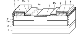
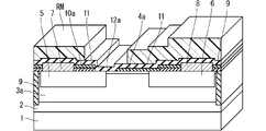
- FIG. 1 is a perspective view showing a cross-sectional configuration of a heterojunction field effect transistor 100 composed of a nitride semiconductor according to the first embodiment of the present invention.
- the heterojunction field effect transistor 100 is a non-doped GaN (non-doped GaN) on a substrate 1 made of silicon carbide (SiC), for example, via a buffer layer 2 made of AlN (aluminum nitride).
- a channel layer 3a composed of a first nitride semiconductor) is laminated, and a high-concentration n-type impurity region 5 (first impurity region) having a high concentration of n-type impurities and a high-concentration n-type impurity region 5 (first impurity region) are formed on the upper layer of the channel layer 3a.
- the high-concentration n-type impurity region 6 (second impurity region) is selectively formed so as to be separated from each other.
- a barrier layer 4a composed of non-doped AlGaN (second nitride semiconductor) forming a heterojunction with the channel layer 3a is formed on the upper layer of the channel layer 3a between the high-concentration n-type impurity regions 5 and 6. Has been done.
- the source electrode 7 and the drain electrode 8 are formed separately from each other on a part of the high-concentration n-type impurity regions 5 and 6, respectively.
- An element separation region 9 extending from the outermost surface of the barrier layer 4a to the inside of the buffer layer 2 is provided on the outer side of each edge portion of the high-concentration n-type impurity regions 5 and 6 on the side opposite to the barrier layer 4a side. ing.
- the device separation region 9 is formed by ion implantation of zinc (Zn).
- a cap insulating film 10a made of SiN a (silicon nitride) is formed so as to cover a part of the region adjacent to the source electrode 7 and the source electrode 7 of the high-concentration n-type impurity region 5. Further, the cap insulating film 10a is formed so as to cover a part of the region adjacent to the drain electrode 8 and the drain electrode 8 of the high-concentration n-type impurity region 6.
- SiO b oxide covers the cap insulating film 10a, the high-concentration n-type impurity region 6 not covered by the cap insulating film 10a, and a part of the barrier layer 4a.
- An electron-supplied insulating film 11 (silicon oxide film) composed of silicon) is formed. Further, the electron supply insulating film 11 is formed so as to cover the cap insulating film 10a on the high concentration n-type impurity region 5 side.
- the electron supply insulating film 11 is provided so that a part of the barrier layer 4a on the high-concentration n-type impurity region 5 side and a part of the adjacent high-concentration n-type impurity region 5 become openings. It is provided.
- the gate insulating film 12a is formed composed of AlO c (aluminum oxide) so as to cover all areas.
- the gate electrode 13 is formed so as to cover the gate insulating film 12a from above a part of the electron supply insulating film 11 on the source electrode 7 side to above the part where the electron supply insulating film 11 on the drain electrode side is formed. ing.
- the channel layer 3a and the barrier layer 4a exclude a region in which a high-concentration n-type impurity region 5, a high-concentration n-type impurity region 6 and an element separation region 9 are formed.
- the doping amount of the elements other than the main elements (Al, Ga and N) constituting these is designed to be at least 1 ⁇ 10 17 cm -3 or less.
- the barrier layer 4a is in a state where the barrier layer 4a is simply formed on the channel layer 3a, that is, a high-concentration n-type impurity region 5, a high-concentration n-type impurity region 6, an element separation region 9, a source electrode 7, and a drain.
- 2DEG two-dimensional electron gas generated at the interface between the channel layer 3a and the barrier layer 4a in a state where the electrode 8, the cap insulating film 10a, the electron supply insulating film 11, the gate insulating film 12a and the gate electrode 13 are not formed.
- the Al composition and thickness are designed so that the sheet resistance Rs ch is a sufficiently high value, that is, at least 1 k ⁇ / sq or more.
- the sheet resistance Rs ch is 10 k.OMEGA / sq That is all.
- the drain current value in the off state of the transistor becomes a sufficiently low value, for example, 1 microampere or less so as not to hinder the operation.
- specific sheet resistance of the barrier layer 4a of the sheet resistance Rs ch state only the barrier layer 4a is formed on the channel layer 3a described above.
- the sheet resistance Rs nd in these regions is set to a value sufficiently low so that the drain current value in the ON state of the transistor does not hinder the operation.
- the doping concentration and thickness are designed to be at least 1 k ⁇ / sq or less. For example, when AlGaN and GaN are doped with donor Si and Ge dopants with an injection dose of 1 ⁇ 10 15 cm- 2 , Rs nd becomes 1 k ⁇ / sq or less.
- the barrier layer 4a sandwiched between the high-concentration n-type impurity region 5 and the high-concentration n-type impurity region 6 is in contact with the gate insulating film 12a on the source electrode 7 side and the electron supply insulating film on the drain electrode 8 side on the upper surface thereof. It is configured to be in contact with 11. That is, the type of insulating film that the barrier layer 4a is in contact with is different between the channel region A in which the barrier layer 4a is in contact with the gate insulating film 12a and the drift region B in which the barrier layer 4a is in contact with the electron supply insulating film 11.
- the 2DEG at the interface between the barrier layer 4a and the channel layer 3a increases in the drift region B, and the drift region It is possible to reduce the sheet resistance Rs dr due to the 2DE generated at the interface between the channel layer 3a and the barrier layer 4a in B to 10 k ⁇ / sq or less. This will be described in detail later.
- the channel layer 3a and the barrier layer 4a sufficiently high value 2DEG generated at the interface is the sheet resistance Rs ch not increased, i.e., it is possible to maintain the value of more than at least 10 k.OMEGA / sq. This will be described in detail later.
- the source electrode 7 is (grounded) with the reference potential, and the voltage (gate voltage) applied to the gate electrode 13 is changed to provide the barrier layer 4a and the channel layer 3a of the channel region A.
- the concentration of 2DEG generated at the interface can be controlled. That is, when the gate voltage is not applied or when the voltage is negative, the concentration of 2DEG is maintained at a sufficiently low state, and even if a positive voltage (drain voltage) is applied to the drain electrode 8, the drain electrode 8 is subjected to. No current (drain current) flows.
- the gate voltage is a positive voltage
- the concentration of 2DEG becomes high, and the resistance is sufficiently low in all regions from the source electrode 7 to the drain electrode 8, so that the positive voltage is applied to the drain electrode 8.
- a large drain current is obtained when That is, the normal off operation is realized as a transistor.
- the drain voltage is increased in the state where the gate voltage is not applied or when the negative voltage is applied (off state), it occurs between the barrier layer 4a and the channel layer 3a in the drift region B. By depleting the 2DEG, the depletion layer extends to the drift region B as well.
- the voltage applied between the gate electrode 13 and the drain electrode 8 is dispersed not only in the gate insulating film 12a but also in the drift region B, and as a result, a large drain voltage can be applied, which is off.
- the withstand voltage at that time becomes high, and high voltage operation of the transistor becomes possible.
- the electron supply insulating film 11 and the gate insulating film 12a are formed on the barrier layer 4a.
- the gate electrode 13 is formed through this order.
- the gate electrode 13 is formed through the electron supply insulating film 11 of b and the gate insulating film 12a of AlOc in this order.
- the source electrode 7 and the drain electrode 8 are covered with the cap insulating film 10a, deterioration due to oxidation of the source electrode 7 and the drain electrode 8 is prevented, and an increase in on-resistance is suppressed. it can.
- the electron supply insulating film 11 is formed on the barrier layer 4a in the drift region B, and the positive charge generated at the interface causes the barrier layer in this region.
- Impurities doped in the barrier layer 4a and the channel layer 3a form a deep energy level in the band gap in the nitride semiconductor and become a trap level that induces current collapse, so that the barrier layer 4a and the channel layer 3a are subjected to. If the doping concentration of the impurities in the above is suppressed sufficiently low, it is possible to suppress the generation of current collapse due to the trap level formed by these.
- Such a trap level has a negligible effect on the current collapse if the level density is sufficiently smaller than the carrier density in the transistor operation, but cannot be ignored if it is formed at the same density.
- Heterojunction field-effect transistors using nitride semiconductors generally use at least 1 ⁇ 10 12 cm- 2 or more 2DEGs as carriers, so the ratio of the effect on current collapse is generally negligible at 1% or less. Then, the trap level density should be 1 ⁇ 10 10 cm- 2 or less.
- the thickness of the barrier layer 4a needs to be 10 nm or less in order to obtain the above-mentioned design value of the sheet resistance, if the doping amount of the barrier layer 4a is 1 ⁇ 10 16 cm -3 or less, the current collapse The effect on is negligible.
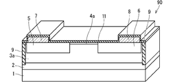
- FIG. 2 is a perspective view showing a cross-sectional configuration of the sample 90 used for verification.
- the same components as those of the heterojunction field effect transistor 100 shown in FIG. 1 are designated by the same reference numerals, and redundant description will be omitted.
- the configuration from the substrate 1 to the source electrode 7 and the drain electrode 8 is the same as that of the heterojunction field effect transistor 100, and is covered by the source electrode 7 and the drain electrode 8, the source electrode 7 and the drain electrode 8.
- An electron supply insulating film 11 is formed so as to cover the surfaces of the high-concentration n-type impurity regions 5 and 6 and the barrier layer 4a.
- the method for producing the sample 90 will be described below.
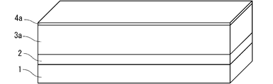
- the buffer layer 2, the channel layer 3a, and the barrier layer 4a are grown in this order on the SiC substrate 1 by the MOCVD (metal organic chemical vapor deposition) method.
- MOCVD metal organic chemical vapor deposition
- two types of structures were used as the barrier layer 4a: when the Al composition and thickness were 15% and 7 nm, and 20% and 5 nm, respectively.
- Si ions are implanted into a desired region under the conditions of an implantation dose amount of 1 ⁇ 10 15 cm- 2 and an implantation energy of 50 keV by the ion implantation method, and then 1150 by the RTA (Rapid Thermal Annealing) method.
- Heat treatment at ° C. for 5 minutes was performed in a nitrogen atmosphere to activate the doped Si ions to form high-concentration n-type impurity regions 5 and 6.
- a source electrode 7 and a drain electrode 8 composed of a metal multilayer film were formed by a vapor deposition and lift-off method.
- Zn is ion-implanted into the channel layer 3a and the barrier layer 4a in the outer regions of the high-concentration n-type impurity region 5 and the high-concentration n-type impurity region 6 by ion implantation to form the device separation region 9. did.
- an electron-supplied insulating film 11 having a thickness of 10 nm was formed by using a plasma CVD method so as to cover all the regions including the barrier layer 4a sandwiched between the high-concentration n-type impurity regions 5 and 6. Further, after the electron-supplied insulating film 11 was formed, a heat treatment was performed in nitrogen at 300 to 950 ° C. for 30 seconds to form a sample 90.
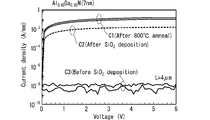
- FIG. 3 and 4 show the current-voltage (IV) characteristics measured between the source electrode 7 and the drain electrode 8 in the sample 90 shown in FIG. 2, and the horizontal axis is the voltage (unit: V). The vertical axis is the current density (unit: A / mm).
- the current value increased significantly (4 digits or more) in both Al compositions. After further heat treatment at 800 ° C., the current value further increased, and a value of about 0.1 A / mm was obtained in both Al compositions.
- the electron-supplied insulating film 11 is represented as SiO b by a compound of Si (silicon) and O (oxygen), but since it is a deposited film, the composition is not necessarily the general SiO 2 . This is because it is not always the case. This also applies to SiN a , AlO c, and the like.
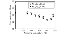
- FIG. 5 shows the heat treatment temperature dependence of the sheet resistance obtained from the IV characteristics measured by using different patterns in the distance between the high-concentration n-type impurity regions 5 and 6 in the range of 2 to 20 ⁇ m. Shown.
- the horizontal axis is the annealing temperature (unit: ° C.) and the vertical axis is the sheet resistance (Sheet resistance: unit ⁇ / sq), and the characteristics when the Al composition and the thickness are 20% and 5 nm, respectively, are shown. It is represented by ⁇ , and the characteristics when the Al composition and thickness are 15% and 7 nm, respectively, are represented by ⁇ .
- both normal-off operation and high withstand voltage operation are realized.
- FIGS. 6 to 15 ⁇ Manufacturing method>
- FIGS. 6 to 15 the same components as those of the heterojunction field effect transistor 100 shown in FIG. 1 are designated by the same reference numerals, and redundant description will be omitted.
- a buffer layer 2 composed of AlN and a channel layer 3a composed of GaN are used on a SiC substrate 1 by an epitaxial growth method such as a MOCVD method or an MBE (Molecular Beam Epitaxy) method. And the barrier layer 4a composed of AlGaN is grown in this order.
- Ions such as Si, which are n-type impurities in physical semiconductors, are implanted in a desired region.
- heat treatment is performed at a temperature of 800 to 1500 ° C. in a nitrogen atmosphere using, for example, the RTA method to activate the doped ions to form a high-concentration n-type impurity region 5 and a high-concentration n-type impurity region 6. To do.
- a metal multilayer film was deposited in a desired region using a vapor deposition and lift-off method, and then heat-treated at a temperature of 500 to 900 ° C. using an RTA method or the like to deposit.
- the multilayer film is alloyed to form the source electrode 7 and the drain electrode 8.
- the metal multilayer film include a multilayer film of Ti (titanium) and Al, but when formed on a high-concentration n-type impurity region, any general metal used as an electrode can be used as an ohmic contact. Is obtained, so there is no particular limitation.
- Zn ions are implanted outside the region where the transistor is formed by using an ion implantation method to form an element separation region 9 that reaches the inside of the buffer layer 2 from the outermost surface of the barrier layer 4a. ..
- the technique of injecting Zn ions to increase the resistance of GaN is well known. For example, Toshiyuki Oishi, Naruhisa Miura, Muneyoshi Suita, Takuma Nanjo, Yuji Abe, and Tatsuo Ozeki J.Appl.Phys.Vol.94, It is disclosed in No. 3 1662-1666 (2003).
- the source electrode 7 and the drain electrode 8 is formed on the channel layer 3a, for example, the cap insulating film 10a composed of SiN a using a plasma CVD method.
- the cap insulating film 10a in a desired region is removed by using a wet etching method using buffered hydrofluoric acid or the like with a resist pattern or the like as a mask.
- the region to be removed is a region from a part of the upper part of the barrier layer 4a to the upper part of the edge portion of the high-concentration n-type impurity region 6 adjacent to the barrier layer 4a.
- SiO is used on the cap insulating film 10a, on the high-concentration n-type impurity region 6 not covered by the cap insulating film 10a, and on the barrier layer 4a of AlGaN, for example, by using the plasma CVD method.
- the electron supply insulating film 11 composed of b is deposited.
- heat treatment at 700 to 900 ° C. is performed in a nitrogen atmosphere using, for example, the RTA method to increase the positive charge generated at the interface of the region where the barrier layer 4a and the electron supply insulating film 11 are in contact with each other.
- the cap insulating film 10a and the electron supply insulating film 11 in the desired region are removed by a wet etching method using buffered hydrofluoric acid or the like with the resist pattern or the like as a mask.
- the region to be removed is a region from a part of the upper part of the barrier layer 4a on the high-concentration n-type impurity region 5 side to the upper end of the high-concentration n-type impurity region 5 adjacent to the barrier layer 4a.
- an atomic layer deposition method is applied on the electron-supplied insulating film 11, the high-concentration n-type impurity region 5 not covered by the electron-supplied insulating film 11, and the barrier layer 4a of AlGaN. depositing a constructed gate insulating film 12a by AlO c using.
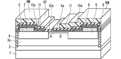
- a resist mask RM is formed on the gate insulating film 12a in which the portion where the gate electrode 13 is to be formed is the opening OP.
- a metal film composed of Ni (nickel) is formed on the resist mask RM and in the opening OP by vapor deposition, and the resist mask RM is removed by a lift-off method to form a gate electrode 13.
- the heterojunction field effect transistor 100 shown in 1 is obtained.
- the cap insulating film 10a shown in FIGS. 10 and 11 is deposited and removed, the electron-supplied insulating film 11 shown in FIG. 12 is deposited, and the temperature is 700 to 900 ° C.
- the heat treatment in FIG. 13, the removal of the cap insulating film 10a and the electron supply insulating film 11 shown in FIG. 13, the deposition of the gate insulating film 12a shown in FIG. 14, and the formation of the gate electrode 13 shown in FIG. 14 are carried out in this order. It is characterized by that.
- the heat treatment at 700 to 900 ° C. is carried out in a state where the barrier layer 4a in the channel region A is covered with the cap insulating film 10a and the barrier layer 4a in the drift region B is covered with the electron supply insulating film 11. become able to.
- the barrier layer 4a When the heat treatment is performed at a high temperature of 700 ° C. or higher, if the barrier layer 4a is exposed to the space for the heat treatment, nitrogen is released from the barrier layer 4a, and nitrogen vacancies that cause electron traps become the barrier layer. Occurs in 4a. In particular, if many such nitrogen vacancies are present in the channel region A, there is concern about an increase in leakage current and deterioration of characteristics such as current collapse. Desorption of nitrogen from the AlGaN layer by such heat treatment can be suppressed by depositing some insulating film on the surface of the AlGaN layer, but it is not completely suppressed and the effect differs depending on the insulating film material used.
- the insulating film composed of SiN a is a material often used as a cap insulating film even during activation heat treatment after ion implantation, and nitrogen from the AlGaN layer is compared with other insulating film materials such as SiO b and AlO c. It is an insulating film material that is highly effective in suppressing the detachment of nitrogen. Therefore, according to this manufacturing method, it is possible to suppress deterioration of characteristics caused by nitrogen vacancies.
- the gate insulating film 12a of the AlO c is because it is formed after the heat treatment at 700 ⁇ 900 ° C., it can be prevented from being subjected to heat treatment at a high temperature.
- the gate insulating film composed of AlO c when heat-treated at a temperature above 700 ° C., partially crystallization proceeds, the grain boundary is known to be a leak path of the current that.
- Even in the heterojunction field effect transistor 100 if the gate insulating film 12a is heat-treated at a high temperature of 700 ° C. or higher, there is a concern that the gate leakage current will increase. However, this manufacturing method can prevent heat treatment at a high temperature, so that a low leakage current is realized.
- a configuration in which the gate electrode 13 is formed on the barrier layer 4a through the electron supply insulating film and the gate insulating film 12a in this order can be formed. ..
- a high voltage is applied to the drain electrode 8
- the gate electrode 13 passes through the cap insulating film 10a, the electron supply insulating film 11 and the gate insulating film 12a in this order on the high-concentration n-type impurity region 5.
- the formed configuration can be formed. As a result, it is possible to alleviate the concentration of the electric field on the end of the gate electrode 13 on the source electrode 7 side when a voltage is applied to the gate electrode 13, and it is possible to suppress the generation of current collapse due to this electric field concentration. ..
- FIG. 1 and the like disclose only the minimum necessary configuration for operating as a transistor
- the device is finally formed through the formation of a protective film, a field plate electrode, wiring, an air bridge, a via hole, and the like. Complete.
- the formation of the high-concentration n-type impurity regions 5 and 6 shown in FIG. 7 does not necessarily have to be performed by the ion implantation method, and may be formed by etching and an epitaxial growth method such as the MOCVD method or the MBE method. ..
- the element separation region 9 shown in FIG. 9 does not necessarily have to be formed by the ion implantation method, and the region reaching the buffer layer 2 is removed from the outermost surface of the barrier layer 4a by etching to prepare a transistor.
- the region to be formed may be a mesa-shaped structure, and the removed region may be an element separation region 9.
- the above-mentioned manufacturing processes do not necessarily have to be carried out in the order described, and the order may be changed.
- the formation of the element separation region 9 shown in FIG. 9 may be performed after the formation of the high-concentration n-type impurity regions 5 and 6 shown in FIG. 7.
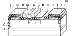
- FIG. 16 is a perspective view showing a cross-sectional configuration of a heterojunction field effect transistor 200 composed of a nitride semiconductor according to the second embodiment of the present invention. Note that, in FIG. 16, the same components as those of the heterojunction field effect transistor 100 described with reference to FIG. 1 are designated by the same reference numerals, and duplicate description will be omitted.
- the heterojunction field-effect transistor 100 shown in FIG. 1 in the region of the lower source electrode 7 side of the gate electrode 13, on the high concentration n-type impurity region 5 of SiN a cap insulating film 10a, the SiO b electronic supplying the insulating film 11 and the gate electrode 13 a gate insulating film 12a through in this order of AlO c is in the formed configuration, the heterojunction field-effect transistor 200 shown in FIG. 16, the high concentration n-type impurity regions
- the gate electrode 13 is formed on the 5 through an electron supply insulating film and a gate insulating film 12a in this order.
- the cap insulating film 10a in a part of the region from the source electrode 7 to the region where the gate electrode 13 is formed is formed. Can be produced by removing the above.
- FIG. 17 is a perspective view showing a cross-sectional configuration of a heterojunction field effect transistor 300 composed of a nitride semiconductor according to the third embodiment of the present invention.
- the same components as those of the heterojunction field effect transistor 100 described with reference to FIG. 1 are designated by the same reference numerals, and redundant description will be omitted.
- the heterojunction field-effect transistor 100 shown in FIG. 17 in the region of the lower source electrode 7 side of the gate electrode 13, on the high concentration n-type impurity region 5 of SiN a cap insulating film 10a, the SiO b electronic supplying the insulating film 11 and the gate electrode 13 a gate insulating film 12a through in this order of AlO c is in the formed configuration, the heterojunction field-effect transistor 300 shown in FIG. 17, the gate electrode 13 is a high concentration
- the n-type impurity region 5 is formed so as to extend from the upper portion of the edge portion of the AlGaN on the barrier layer 4a side to the upper portion of the central portion of the barrier layer 4a, and the width is narrowed.
- the edge portion of the gate electrode 13 on the source electrode 7 side is located above the high-concentration n-type impurity region 5 via the gate insulating film 12a. That is, in the region on the source electrode 7 side below the gate electrode 13, the gate electrode 13 is formed on the gate insulating film 12a as in the barrier layer 4a which is the channel region A, and has an electric field relaxation structure. is not.
- the source electrode 7 side of the gate electrode 13 when a voltage is applied to the drain electrode 8 The effect of relaxing the concentration of the electric field at the end of the is weakened. Therefore, the effect of suppressing the generation of current collapse due to the concentration of the electric field is also reduced.
- the region where the gate electrode 13 and the high-concentration n-type impurity region 5 overlap can be reduced.
- the gate capacitance is increased by that amount and switching at high speed becomes difficult.
- the heterojunction field effect transistor 300 the gate capacitance is increased. Can be reduced.
- the edge portion of the gate electrode 13 on the drain electrode 8 side is located on the laminated film of the electron supply insulating film 11 and the gate insulating film 12a, so that it has an electric field relaxation structure. There is.
- the heterojunction field effect transistor 300 is advantageous in that the effect of reducing the gate capacitance can be obtained when the high voltage operation and the occurrence of current collapse are sufficiently suppressed by this alone.
- any of the heterojunction field effect transistors 100 to 300 may be adopted according to the desired operating conditions of the transistor.
- the width of the opening OP of the resist mask RM is narrowed at the time of forming the gate electrode 13 described with reference to FIG. 15, and the gate electrode 13 has a high concentration n type.
- the impurity region 5 may be formed from the upper portion of the edge portion of the AlGaN on the barrier layer 4a side to the upper portion of the central portion of the barrier layer 4a.
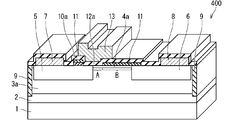
- FIG. 18 is a perspective view showing a cross-sectional configuration of a heterojunction field effect transistor 400 composed of a nitride semiconductor according to the fourth embodiment of the present invention. Note that, in FIG. 18, the same components as those of the heterojunction field effect transistor 100 described with reference to FIG. 1 are designated by the same reference numerals, and duplicate description will be omitted.
- the source electrode 7 and the drain electrode 8 cap insulating film 10a of the SiN a, a layered film of the gate insulating film 12a of the electron supply insulating film 11 and the AlO c of SiO b
- the configuration is covered, in the heterojunction field effect transistor 400, the source electrode 7 and the drain electrode 8 are covered only with the gate insulating film 12a.
- the edge portion of the gate electrode 13 on the source electrode 7 side is located above the high-concentration n-type impurity region 5 via the cap insulating film 10a, the electron supply insulating film 11 and the gate insulating film 12a. That is, the cap insulating film 10a and the electron supply insulating film 11 are laminated in this order only on the high-concentration n-type impurity region 5 below the edge portion on the source electrode 7 side of the gate electrode 13, and the laminated film is gate-insulated.
- the film 12a covers it.
- the edge portion of the gate electrode 13 on the drain electrode 8 side is located above the barrier layer 4a via the electron supply insulating film 11 and the gate insulating film 12a.
- the heterojunction field effect transistor 400 having such a configuration can achieve both normal off operation and high withstand voltage operation.
- the concentration of the lower part of the edge portion of the gate electrode 13 on the source electrode 7 side is high.
- the cap insulating film 10a is removed so that the cap insulating film 10a remains only on the n-type impurity region 5.
- the region from the upper part of the barrier layer 4a to the upper part of the edge portion of the high-concentration n-type impurity region 6 and the high-concentration n-type may be removed so that the electron-supplied insulating film 11a remains only on the upper portion of the cap insulating film 10a on the impurity region 5.
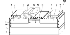
- FIG. 19 is a perspective view showing a cross-sectional configuration of a heterojunction field effect transistor 401 composed of a nitride semiconductor according to the first modification of the fourth embodiment according to the present invention. Note that, in FIG. 19, the same components as those of the heterojunction field effect transistor 400 described with reference to FIG. 18 are designated by the same reference numerals, and redundant description will be omitted.
- the edge portion of the gate electrode 13 on the source electrode 7 side has a high concentration n-type via a cap insulating film 10a, an electron supply insulating film 11 and a gate insulating film 12a. Although it was located above the impurity region 5, in the heterojunction field effect transistor 401, the edge portion of the gate electrode 13 on the source electrode 7 side has a high concentration via the electron supply insulating film 11 and the gate insulating film 12a. It is located above the n-type impurity region 5.
- an electron-supplied insulating film 11 is formed on the high-concentration n-type impurity region 5 below the edge portion of the gate electrode 13 on the source electrode 7 side, and the electron-supplied insulating film 11 is covered with the gate insulating film 12a. There is.
- the edge of the gate electrode 13 on the drain electrode 8 side is located above the barrier layer 4a via the electron supply insulating film 11 and the gate insulating film 12a, so that the heterojunction field effect transistor 400 is used. It is the same.
- the manufacturing step of the cap insulating film 10a described with reference to FIG. 11 becomes unnecessary, and the electron-supplied insulating film 11a using the resist pattern described with reference to FIG. 13 is removed.
- the electron-supplied insulating film 11 may be removed so that the electron-supplied insulating film 11 remains.
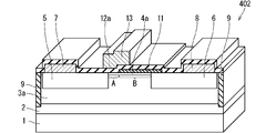
- FIG. 20 is a perspective view showing a cross-sectional configuration of a heterojunction field effect transistor 402 composed of a nitride semiconductor according to a modification 2 of the fourth embodiment according to the present invention.
- the same components as those of the heterojunction field effect transistor 400 described with reference to FIG. 18 are designated by the same reference numerals, and redundant description will be omitted.
- the edge portion of the gate electrode 13 on the source electrode 7 side has a high concentration n-type via the cap insulating film 10a, the electron supply insulating film 11 and the gate insulating film 12a. Although it was located above the impurity region 5, in the heterojunction field effect transistor 402, the edge of the gate electrode 13 on the source electrode 7 side is the high-concentration n-type impurity region 5 via the gate insulating film 12a. It is located at the top.
- the edge of the gate electrode 13 on the drain electrode 8 side is located above the barrier layer 4a via the electron supply insulating film 11 and the gate insulating film 12a, so that the heterojunction field effect transistor 400 is used. It is the same.
- the gate electrode 13 is formed so as to extend from the upper portion of the edge portion of the AlGaN of the high-concentration n-type impurity region 5 on the barrier layer 4a side to the upper portion of the central portion of the barrier layer 4a, and the width becomes narrower. There is. That is, since the edge portion of the gate electrode 13 on the source electrode 7 side does not have an electric field relaxation structure, the width of the gate electrode 13 is narrowed in order to reduce the gate capacitance.
- the manufacturing step of the cap insulating film 10a described with reference to FIG. 11 becomes unnecessary, and the electron-supplied insulating film 11a using the resist pattern described with reference to FIG. 13 is removed.
- the electron-supplied insulating film 11 may be removed so that the electron-supplied insulating film 11 remains.
- the gate electrode 13 described with reference to FIG. 15 when the gate electrode 13 described with reference to FIG. 15 is formed, the width of the opening OP of the resist mask RM is narrowed, and the gate electrode 13 is the edge of the AlGaN barrier layer 4a side of the high-concentration n-type impurity region 5. It may be formed from the upper part of the portion to the upper part of the central portion of the barrier layer 4a.
- the material constituting the source electrode 7 and the drain electrode 8 is used when the cap insulating film 10a and the electron supply insulating film 11 are removed. It is an effective configuration when it is resistant to acid.
- the heterojunction field effect transistors 100 to 300 of the first to third embodiments may be adopted.
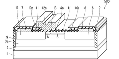
- FIG. 21 is a perspective view showing a cross-sectional configuration of a heterojunction field effect transistor 500 composed of a nitride semiconductor according to the fifth embodiment of the present invention.
- the same components as those of the heterojunction field effect transistor 100 described with reference to FIG. 1 are designated by the same reference numerals, and redundant description will be omitted.
- the source electrode 7 and the drain electrode 8 cap insulating film 10a of the SiN a, a layered film of the gate insulating film 12a of the electron supply insulating film 11 and the AlO c of SiO b
- the heterojunction field effect transistor 500 the upper surfaces of the source electrode 7 and the drain electrode 8 are covered only with the gate insulating film 12a, and the cap insulating film 10a and the electron supply insulating film 11 are covered.
- the laminated film of the gate insulating film 12a is in contact with the side surfaces of the source electrode 7 and the drain electrode 8.
- it is the same as the heterojunction field effect transistor 100, and like the heterojunction field effect transistor 100, both normal-off operation and high withstand voltage operation are realized.
- FIGS. 6, 7, and 22 to 29 show the manufacturing process in order.
- FIGS. 22 to 29 the same components as those of the heterojunction field effect transistor 100 shown in FIG. 1 are designated by the same reference numerals, and redundant description will be omitted.
- the buffer layer 2 composed of AlN and the GaN are formed on the SiC substrate 1 by using an epitaxial growth method such as the MOCVD method or the MBE method.
- the barrier layer 4a composed of the channel layer 3a and AlGaN is grown in this order.
- the injection dose amount is 1 ⁇ 10 13 to 1 ⁇ 10 16 cm- 2
- the implantation energy is used by using the ion implantation method or the like with the resist pattern or the like as a mask.
- ions such as Si, which is an n-type impurity in the nitride semiconductor, are implanted in a desired region.
- heat treatment is performed at a temperature of 800 to 1500 ° C. in a nitrogen atmosphere using, for example, the RTA method to activate the doped ions to form a high-concentration n-type impurity region 5 and a high-concentration n-type impurity region 6. To do.
- Zn ions are implanted outside the region where the transistor is formed by using an ion implantation method to form an element separation region 9 that reaches the inside of the buffer layer 2 from the outermost surface of the barrier layer 4a. ..
- a technique of injecting Zn ions to increase the resistance of GaN is well known.
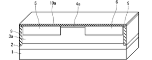
- the element isolation region 9, the high-concentration n-type impurity regions 5 and 6 are formed in the channel layer 3a, for example, the cap insulating film composed of SiN a using a plasma CVD method 10a is deposited.
- the cap insulating film 10a in a desired region is removed by using a wet etching method using buffered hydrofluoric acid or the like with a resist pattern or the like as a mask.
- the region to be removed is a region from a part of the upper part of the barrier layer 4a to the upper part of the edge portion of the high-concentration n-type impurity region 6 adjacent to the barrier layer 4a.
- SiO is used on the cap insulating film 10a, on the high-concentration n-type impurity region 6 not covered by the cap insulating film 10a, and on the barrier layer 4a of AlGaN, for example, by using the plasma CVD method.
- the electron supply insulating film 11 composed of b is deposited.
- a resist mask having an opening in the region forming the source electrode 7 and the drain electrode 8 was formed on the electron supply insulating film 11, and buffered phosphoric acid or the like was used using the resist mask as an etching mask.
- a wet etching method is used to remove the electron supply insulating film 11 and the cap insulating film 10a in the region where the source electrode 7 and the drain electrode 8 are formed.
- a metal multilayer film is deposited on the etching mask and on the opening by vapor deposition, and the etching mask is removed by a lift-off method to leave a metal multilayer film in the region where the source electrode 7 and the drain electrode 8 are formed. ..
- heat treatment is performed at a temperature of 700 to 900 ° C. in a nitrogen atmosphere using the RTA method or the like, and the deposited multilayer film is alloyed to form the source electrode 7 and the drain electrode 8.
- the positive charge generated at the interface of the region where the barrier layer 4a and the electron supply insulating film 11 are in contact with each other is increased.
- the metal multilayer film examples include a multilayer film of Ti (titanium) and Al, but when formed on a high-concentration n-type impurity region, any general metal used as an electrode can be used as an ohmic contact. Is obtained, so there is no particular limitation.
- the cap insulating film 10a and the electron-supplied insulating film 11 in a desired region are removed by a wet etching method using buffered hydrofluoric acid or the like with the resist pattern or the like as a mask.
- the region to be removed is a region from a part of the upper part of the barrier layer 4a on the high-concentration n-type impurity region 5 side to the upper end of the high-concentration n-type impurity region 5 adjacent to the barrier layer 4a.
- the electron-supplied insulating film 11 on the electron-supplied insulating film 11, the upper surfaces of the source electrode 7 and the drain electrode 8 not covered with the electron-supplied insulating film 11, the high-concentration n-type impurity region 5 and the barrier layer 4a. to, depositing the formed gate insulating film 12a by AlO c using, for example, atomic layer deposition.
- a resist mask RM is formed on the gate insulating film 12a in which the portion where the gate electrode 13 is to be formed is the opening OP.
- a metal film composed of Ni is formed on the resist mask RM and in the opening OP by vapor deposition, and the resist mask RM is removed by a lift-off method to form a gate electrode 13, which is shown in FIG.
- a heterojunction field effect transistor 500 is obtained.
- the source electrode 7 and the drain electrode 8 are formed after the electron supply insulating film 11 shown in FIG. 25 is deposited. It is a process. As a result, the source electrode 7 and the drain electrode 8 are not exposed to the hydrofluoric acid used when removing the cap insulating film 10a and the electron supply insulating film 11, and the material constituting the source electrode 7 and the drain electrode 8 is formed. However, the manufacturing process is suitable when there is no resistance to hydrofluoric acid.
- FIG. 30 is a perspective view showing a cross-sectional configuration of a heterojunction field effect transistor 600 composed of a nitride semiconductor according to the sixth embodiment of the present invention.
- the same components as those of the heterojunction field effect transistor 200 described with reference to FIG. 16 are designated by the same reference numerals, and redundant description will be omitted.
- the heterojunction field-effect transistor 600 shown in FIG. 30 has a higher concentration n-type impurity region 5 than the heterojunction field-effect transistor 100 shown in FIG. 1 and the heterojunction field-effect transistor 200 shown in FIG.
- the regions where are formed are different. That is, in the heterojunction field effect transistors 100 and 200, the high concentration n-type impurity region 5 is formed from the region below the source electrode 7 to the region below the gate electrode 13, but the heterojunction field effect transistor is formed.
- the edge portion of the high-concentration n-type impurity region 5 on the gate electrode 13 side is formed so as not to reach the region below the gate electrode. That is, the high-concentration n-type impurity region 5 is not formed below the edge portion of the gate electrode 13 on the source electrode 7 side.
- the heterojunction field effect transistor 600 having such a configuration also realizes both normal off operation and high withstand voltage operation.
- the sheet resistance is compared with the sheet resistance due to 2DEG generated between the barrier layer 4a and the channel layer 3a.
- the on-resistance of the heterojunction field-effect transistor 600 in which a low value is obtained and the high-concentration n-type impurity region 5 does not reach below the gate electrode 13 can be higher than that of the heterojunction field-effect transistors 100 and 200. There is sex.
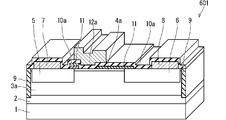
- FIG. 31 is a perspective view showing a cross-sectional configuration of a heterojunction field effect transistor 601 composed of a nitride semiconductor according to a modification of the sixth embodiment of the present invention.
- the same components as those of the heterojunction field effect transistor 600 described with reference to FIG. 30 are designated by the same reference numerals, and duplicate description will be omitted.
- the source electrode 7 and the drain electrode 8 cap insulating film 10a of the SiN a, a layered film of the gate insulating film 12a of the electron supply insulating film 11 and the AlO c of SiO b
- the configuration is covered, in the heterojunction field effect transistor 601 the source electrode 7 and the drain electrode 8 are covered only with the gate insulating film 12a.
- the edge portion of the gate electrode 13 on the source electrode 7 side is above the boundary between the high-concentration n-type impurity region 5 and the barrier layer 4a via the cap insulating film 10a, the electron supply insulating film 11 and the gate insulating film 12a. Is located in. That is, the cap insulating film 10a and the electron supply insulating film 11 are laminated in this order only on the lower portion of the edge portion of the gate electrode 13 on the source electrode 7 side, and the laminated film is covered with the gate insulating film 12a.
- the heterojunction field effect transistor 601 having such a configuration also realizes both normal off operation and high withstand voltage operation.
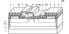
- FIG. 32 is a perspective view showing a cross-sectional configuration of a heterojunction field effect transistor 700 composed of a nitride semiconductor according to the seventh embodiment of the present invention.
- the same components as those of the heterojunction field effect transistor 100 described with reference to FIG. 1 are designated by the same reference numerals, and redundant description will be omitted.
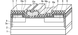
- the heterojunction field-effect transistor 100 shown in FIG. 1 has a configuration in which a gate insulating film 12a is formed on the outermost surface except for the region where the gate electrode 13 is formed. in 700, it has a structure in which the gate electrode 13 and the gate insulating film 12a is covered with the formed coating insulating film 14a by SiN d. This makes it possible to prevent a decrease in the drain current when the heat treatment is performed after the gate electrode 13 is formed. This will be described in detail below.
- the drain current may decrease due to the formation of an interface state between the gate insulating film 12a under the gate electrode 13 and the barrier layer 4a. ..
- This interface state can be reduced by heat-treating at 300 to 700 ° C. after forming the gate electrode 13, as disclosed in International Publication No. 2018/037530. Further, as disclosed in International Publication No. 2018/220741, the reduction can be achieved by forming the gate electrode 13 and then performing a heat treatment at 250 to 300 ° C. while applying a voltage to the gate electrode 13. ..
- the gate insulating film 12a is the most in the drift region B after the gate electrode 13 is formed.
- the concentration of 2DEG generated at the interface between the channel layer 3a and the barrier layer 4a in the drift region B decreases, and as a result of increasing the resistance in this region, the drain current decreases. It ends up.
- the sheet resistance Rs ch in 2DEG generated at the interface between the channel layer 3a and the barrier layer 4a by the gate insulating film 12a is performed a heat treatment in a state of being formed on the outermost surface in the drift region B increases and by the gate insulating film 12a is configured covered with configured coating insulating film 14a by SiN d, shows the results of increase in the sheet resistance Rs ch has validated the phenomena are suppressed.
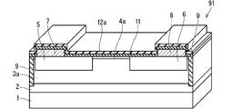
- FIG. 33 and 34 are perspective views showing the cross-sectional configurations of the sample 91 and the sample 92 used for the verification.
- the same components as those of the sample 90 shown in FIG. 2 are designated by the same reference numerals, and redundant description will be omitted.
- the configuration from the substrate 1 to the electron supply insulating film 11 is the same as that of the sample 90, and the gate insulating film 12a is formed so as to cover the surface of the electron supply insulating film 11.
- Such a configuration can be fabricated by depositing the formed gate insulating film 12a by AlO c using on the electron supply insulating film 11 on the surface of the sample 90 shown in Figure 2, for example, atomic layer deposition method It becomes.
- the configuration from the substrate 1 to the gate insulating film 12a is the same as that of the sample 91, and a coated insulating film 14a composed of SiN d is formed so as to cover the surface of the gate insulating film 12a.
- Such a configuration can be produced by depositing a coated insulating film 14a composed of SiN d on the gate insulating film 12a on the surface of the sample 91 shown in FIG. 33, for example, by using a plasma CVD method. ..
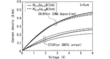
- 35 and 36 are current-voltage (IV) characteristics measured between the source electrode 7 and the drain electrode 8 in the sample 91 shown in FIG. 33 and the sample 92 shown in FIG. 34, respectively.
- the voltage (Voltage: unit V) and the vertical axis are the current density (Current density: unit A / mm).
- FIG. 35 shows the measurement result C4 (After Al 2 O 3 deposition) immediately after the gate insulating film 12a was deposited and the measurement result C5 (After 300 ° C.) after heat treatment at 300 ° C. for 5 minutes after the gate insulating film 12a was deposited. Anneal) is shown. Since two samples are prepared and measured on the same substrate, both measurement results show two characteristics.
- FIG 36 the coating insulating film 14a at immediately after deposition of the measurement results C6 (After SiN d deposition) and the covering insulating film 14a is deposited after the measurement of after heat-treated for 5 minutes at 300 ° C.
- Results C7 After 300 °C Anneal Is shown. Since two samples are prepared and measured on the same substrate, both measurement results show two characteristics.
- FIGS. 35 and 36 show the characteristics of the barrier layer 4a when the Al composition and thickness are 20% and 5 nm, respectively, and when the Al composition and thickness are 15% and 7 nm, respectively.
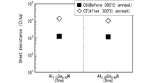
- the coating insulating film 14a has an effect of suppressing a decrease in positive charges induced at the interface between SiO b and AlGaN.
- the coating insulating film 14a is represented as SiN d by a compound of Si (silicon) and N (nitrogen), but since it is a sedimentary film, the composition is not necessarily Si 3 N 4 which is general. This is because it is not always present.
- the sheet resistance (Sheet resistance) obtained from the IV characteristics measured using different patterns in the range where the distance between the high-concentration n-type impurity regions 5 and 6 is in the range of 2 to 20 ⁇ m is shown. : Unit ⁇ / sq) is shown.
- FIG. 37 shows the sheet resistance of the sample 91 shown in FIG. 33 before and after the heat treatment at 300 ° C., respectively
- FIG. 38 shows the sheet resistance of the sample 92 shown in FIG. 34 before and after the heat treatment at 300 ° C., respectively. Expressed as ⁇ and ⁇ .
- both normal-off operation and high withstand voltage operation are realized.
- the heterojunction field effect transistor 100 shown in FIG. 1 is obtained.
- a coated insulating film 14a composed of SiN d is deposited on the gate electrode 13 and the gate insulating film 12a by using, for example, a plasma CVD method to obtain the heterojunction field effect transistor 700 shown in FIG. ..
- heat treatment is performed at at least 300 ° C. for the purpose of reducing the interface state formed between the gate insulating film 12a and the barrier layer 4a.
- FIG. 39 is a perspective view showing a cross-sectional configuration of a heterojunction field effect transistor 701 composed of a nitride semiconductor according to the first modification of the seventh embodiment according to the present invention.
- the same components as those of the heterojunction field effect transistor 700 described with reference to FIG. 32 are designated by the same reference numerals, and redundant description will be omitted.
- the coating insulating film 14a is formed so as to cover the entire region of the transistor 700, whereas in the heterojunction field effect transistor 701 shown in FIG. 39, the coating insulation is provided.
- the film 14a is provided so as to be embedded between the side surface of the gate electrode 13 and the side surface of the stepped portion of the gate insulating film 12a, and is formed so as to cover the upper side of the drift region B.
- Such a configuration can be obtained by forming the heterojunction field effect transistor 700 and then selectively removing the coating insulating film 14a.
- the decrease in drain current due to heat treatment after forming the gate insulating film 12a is caused by an increase in resistance in the drift region B, if at least this region is covered with the coating insulating film 14a, the decrease in drain current can be suppressed. It will be possible.
- FIG. 40 is a perspective view showing a cross-sectional configuration of a heterojunction field effect transistor 702 composed of a nitride semiconductor according to a modification 2 of the seventh embodiment according to the present invention.
- the heterojunction field effect transistor 600 of the sixth embodiment is provided with the coating insulating film 14a, and in FIG. 40, the heterojunction field effect transistor 600 described with reference to FIG. 30 is used.
- the same reference numerals are given to the same configurations, and duplicate description will be omitted.
- the heterojunction field-effect transistor 600 shown in FIG. 30 has a higher concentration n-type impurity region 5 than the heterojunction field-effect transistor 100 shown in FIG. 1 and the heterojunction field-effect transistor 200 shown in FIG.
- the regions where are formed are different. That is, in the heterojunction field effect transistors 100 and 200, the high concentration n-type impurity region 5 is formed from the region below the source electrode 7 to the region below the gate electrode 13, but the heterojunction field effect transistor is formed.
- the edge portion of the high-concentration n-type impurity region 5 on the gate electrode 13 side is formed so as not to reach the region below the gate electrode. That is, the high-concentration n-type impurity region 5 is not formed below the edge portion of the gate electrode 13 on the source electrode 7 side.
- the resistance is increased even in the region from the high-concentration n-type impurity region 5 to the lower side of the gate electrode 13 by performing the heat treatment after forming the gate insulating film 12a. And the drain current decreases.
- the coating insulating film 14a is formed so as to cover the entire region of the heterojunction field effect transistor 700, and the upper portion of the region is covered with the coating insulating film 14a.
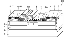
- FIG. 41 is a perspective view showing a cross-sectional configuration of a heterojunction field effect transistor 800 composed of a nitride semiconductor according to the eighth embodiment of the present invention.
- the same components as those of the heterojunction field effect transistor 100 described with reference to FIG. 1 are designated by the same reference numerals, and duplicate description will be omitted.
- the channel layer 3a is composed of GaN and the barrier layer 4a is composed of AlGaN, but GaN and AlGaN must be used.
- the effect exhibited by the heterojunction field effect transistors of the first to seventh embodiments can be obtained even if the channel layer and the barrier layer are made of a nitride semiconductor other than GaN and AlGaN.
- the heterojunction electric field effect transistor 800 shown in FIG. 41 has a channel layer 3a made of GaN and a barrier layer 4a made of AlGaN, respectively, with Al x1 In y1 Ga 1-x1-y1 N (aluminum indium gallium nitride). ) And the barrier layer 4 composed of Al x2 In y2 Ga 1-x2-y2 N. It is assumed that the Al x2 In y2 Ga 1-x2-y2 N constituting the barrier layer 4 has a larger bandgap than the Al x1 In y1 Ga 1-x1-y1 N constituting the channel layer 3.
- the heterojunction field effect transistor 800 instead of the growth of the channel layer 3a and the barrier layer 4a described with reference to FIG. 6, In z Al x Ga 1-x-z N (0 ⁇ x ⁇ 1, 0 ⁇ z). By adjusting the flow rate, pressure and temperature (growth conditions) of trimethylindium, trimethylaluminum, trimethylgallium, ammonia and the like as the raw material gas of ⁇ 1) to grow the channel layer 3 and the barrier layer 4, each desired composition is obtained. It is obtained by forming the channel layer 3 and the barrier layer 4 of the above.
- FIG. 42 is a perspective view showing a cross-sectional configuration of a heterojunction field effect transistor 900 composed of a nitride semiconductor according to a ninth embodiment of the present invention.
- the same components as those of the heterojunction field effect transistor 100 described with reference to FIG. 1 are designated by the same reference numerals, and duplicate description will be omitted.
- the cap insulating film 10a has been described as being composed of SiN a, in carrying out heat treatment at more than 700 ° C.
- the barrier layer if it is possible to suppress the desorption of nitrogen from the nitride semiconductor forming the cap insulating film need not composed necessarily SiN a, as shown in FIG. 42, for example AlN d (aluminum nitride) or BN e
- a cap insulating film 10 composed of an insulating film such as (boron nitride) or a semiconductor film may be used.
- the heterojunction field effect transistor 900 having such a configuration has the same effect as that of the heterojunction field effect transistors of the first to eighth embodiments.
- AlN d or BN e is deposited by a sputtering method or the like using a target composed of Al or B, instead of the deposition of the cap insulating film 10a described with reference to FIG. It is obtained by forming the cap insulating film 10.
- FIG. 43 is a perspective view showing a cross-sectional configuration of a heterojunction field effect transistor 1000 composed of a nitride semiconductor according to the tenth embodiment of the present invention.
- the same components as those of the heterojunction field effect transistor 100 described with reference to FIG. 1 are designated by the same reference numerals, and duplicate description will be omitted.
- the gate insulating film 12a has been described as being composed of AlO c
- the barrier layer is Al x1 In y1 Ga 1-x1 -y1 N
- AlO c may be used AlGa f O a N g gate insulating film 12 made of a (aluminum oxynitride gallium).
- the heterojunction field effect transistor 1000 having such a configuration has the same effect as that of the heterojunction field effect transistors of the first to ninth embodiments.
- heterojunction field effect transistor 1000 instead of the deposition of the gate insulating film 12a described with reference to FIG. 14, trimethylaluminum, trimethylgallium, oxygen, ozone, nitrogen, etc., which are raw materials for the gate insulating film, are flowed and used. pressure, by adjusting the temperature (deposition conditions) obtained by forming a AlGa f O a N g the depositing the gate insulating film 12.
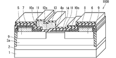
- FIG. 44 is a perspective view showing a cross-sectional configuration of a heterojunction field effect transistor 1100 composed of a nitride semiconductor according to the eleventh embodiment of the present invention.
- the same components as those of the heterojunction field effect transistor 100 described with reference to FIG. 1 are designated by the same reference numerals, and duplicate description will be omitted.
- the coating insulating film 14a has been described as being composed of SiN d, by heat treatment after forming the gate insulating film 12, SiO b and AlGaN If it is possible to suppress the decrease of the positive charge induced at the interface with, it does not necessarily have to be composed of SiN d , and as shown in FIG. 44, for example, AlN d (aluminum nitride) or BN e ( A coated insulating film 14 composed of an insulating film such as (boron nitride) or a semiconductor film may be used.
- the heterojunction field-effect transistor 1100 having such a configuration has the same effect as that of the heterojunction field-effect transistor of the seventh embodiment.
- AlN d or BN e is deposited by a sputtering method or the like using a target composed of Al or B, instead of the deposition of the coated insulating film 14a described with reference to FIG. 32. It is obtained by forming the coating insulating film 14.
- FIG. 45 is a perspective view showing a cross-sectional configuration of a heterojunction field effect transistor 1200 composed of a nitride semiconductor according to the twelfth embodiment of the present invention.
- the same components as those of the heterojunction field effect transistor 100 described with reference to FIG. 1 are designated by the same reference numerals, and duplicate description will be omitted.
- the channel layer 3 is composed of Al x1 In y1 Ga 1-x1-y1 N, but the heterojunction field effect shown in FIG. 45
- the channel layer 3b composed of Al x1 Ga 1-x1 N in this way, the configuration including the channel layer 3 composed of Al x1 In y1 Ga 1-x1-y1 N composed of four elements is provided. Since the alloy scattering received by the electrons traveling on the hetero interface between the channel layer 3b and the barrier layer 4a as carriers is suppressed, the mobility of the electrons in the channel formed at the hetero interface is improved. The drain current can be increased.
- x1 is in the range of x1 ⁇ 1 in principle, but in reality, the difference in Al composition ratio from the barrier layer needs to be several percent, so when the barrier layer is AlN.
- X1 is in the range of 0.97 to 0.98. In addition to this, the mobility and electron concentration will be adjusted to the desired values to determine x1 and other compositions.
- alloy scattering is further suppressed as compared with the configuration including the channel layer 3b composed of Al x1 Ga 1-x1 N composed of three elements. Therefore, the mobility of electrons in the channel formed at the hetero interface is further improved, and the drain current can be further increased.
- crystal growth is further facilitated, and impurities unintentionally mixed in the channel layer 3a can be reduced, so that current collapse caused by electron traps due to these impurities can be suppressed. Further, by further facilitating crystal growth, it is easy to reduce defects in the crystal, and various characteristics such as leakage current and current collapse generated by the defects can be improved.
- the material constituting the channel layer so as to compare the configuration of FIG. 41 with the configuration of FIG. 45 and the configuration of FIG. 1 with the configuration of FIG. 45 has been described, but other embodiments have been described. Needless to say, by replacing the channel layer with the channel layer 3b, the same effect as that of the heterojunction field effect transistor 1200 of the present embodiment can be obtained.
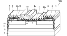
- FIG. 46 is a perspective view showing a cross-sectional configuration of a heterojunction field effect transistor 1300 composed of a nitride semiconductor according to the thirteenth embodiment of the present invention.
- the same components as those of the heterojunction field effect transistor 100 described with reference to FIG. 1 are designated by the same reference numerals, and redundant description will be omitted.
- the heterojunction field effect transistor 800 shown in FIG. 41 includes a barrier layer 4 composed of Al x2 In y2 Ga 1-x2-y2 N, whereas the heterojunction field effect transistor 1300 shown in FIG. 46 has a barrier layer 4.
- the barrier layer 4a composed of Al x2 Ga 1-x2 N
- the alloy scattering received by the electrons traveling on the hetero interface between the channel layer 3 and the barrier layer 4a as a carrier is reduced.
- the mobility of electrons in the channel formed at the hetero interface is improved, and the drain current can be increased.
- the number of constituent elements of the barrier layer is reduced, crystal growth is facilitated, so that defects in the crystal can be easily reduced, and various characteristics such as leakage current and current collapse generated by the defects can be improved.
- FIG. 47 is a perspective view showing a cross-sectional configuration of a heterojunction field effect transistor 1301 composed of a nitride semiconductor according to the first modification of the thirteenth embodiment according to the present invention.
- the same components as those of the heterojunction field effect transistor 1100 described with reference to FIG. 46 are designated by the same reference numerals, and redundant description will be omitted.
- the heterojunction field-effect transistor 800 shown in FIG. 41 includes a barrier layer 4 composed of Al x2 In y2 Ga 1-x2-y2 N, whereas the heterojunction field-effect transistor 1301 shown in FIG. 47 has a barrier layer 4.
- a barrier layer 4b composed of In y2 Al y2 N (x2 + y2 1) is provided instead of the barrier layer 4.
- the barrier layer 4b composed of In y2 Al y2 N
- the alloy scattering received by the electrons traveling on the hetero interface between the channel layer 3 and the barrier layer 4b as carriers is reduced, so that the hetero
- the mobility of electrons in the channel formed at the interface is improved, and the drain current can be increased.
- the number of constituent elements of the barrier layer is reduced, crystal growth is facilitated, so that defects in the crystal can be easily reduced, and various characteristics such as leakage current and current collapse generated by the defects can be improved.
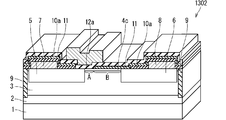
- FIG. 48 is a perspective view showing a cross-sectional configuration of a heterojunction field effect transistor 1302 composed of a nitride semiconductor according to a modification of Embodiment 13 according to the present invention.
- the same components as those of the heterojunction field effect transistor 1300 described with reference to FIG. 46 are designated by the same reference numerals, and redundant description will be omitted.
- the heterojunction field-effect transistor 800 shown in FIG. 41 includes a barrier layer 4 composed of Al x2 In y2 Ga 1-x2-y2 N, whereas the heterojunction field-effect transistor 1302 shown in FIG. 48 has a barrier layer 4.
- the barrier layer 4c composed of AlN
- the alloy scattering received by the electrons traveling with the hetero interface between the channel layer 3 and the barrier layer 4c as a carrier is further reduced, so that the barrier layer 4c is formed at the hetero interface.
- the mobility of electrons in the channel is further improved.
- the number of constituent elements of the barrier layer is reduced, crystal growth is facilitated, so that defects in the crystal can be easily reduced, and various characteristics such as leakage current and current collapse generated by the defects can be improved.
- the materials constituting the barrier layer are described so as to compare the configuration of FIG. 41 with the configurations of FIGS. 46 to 48, but the barrier layer of another embodiment is referred to as the barrier layer 4b or 4c. Needless to say, by replacing with, the same effect as that of the heterojunction field effect transistor 1300 to 1302 of the present embodiment can be obtained.
- the buffer layer is not always necessary. is not it. Further, the buffer layer does not necessarily have to be non-doped.
- the minimum effect described in the first to thirteenth embodiments can be obtained, and the normal off operation and high performance can be obtained. Both pressure-resistant operation is realized.
- heterojunction field effect transistors of the first to thirteenth embodiments describe only the minimum semiconductor layer that operates as a transistor, but other semiconductor layers may be formed as long as they operate as a transistor. Absent.
- a nitride semiconductor layer having a composition different from that of the channel layer and the barrier layer may be formed below the channel layer.
- the nitride semiconductor layer other than the channel layer and the barrier layer does not necessarily have to be non-doped, and Si, Mg (magnesium), Fe (iron), C and Ge (germanium) as long as they do not interfere with the transistor operation. ) And other impurities may be included.
- n-type impurities that are doped in the high-concentration n-type impurity region 5 and the high-concentration n-type impurity region 6 are impurities that behave as n-type dopants in nitride semiconductors such as Si, Ge, oxygen, and nitrogen vacancies. All you need is.
- the cap insulating film 10 is formed on the upper side of the barrier layer 4, the high-concentration n-type impurity region 5, the high-concentration n-type impurity region 6, the source electrode 7, the drain electrode 8, and the like. If it is formed in a region for achieving the purpose of forming the electric field relaxation structure and protecting the surface of the barrier layer during heat treatment according to the first to thirteenth forms, even if it is formed in other regions, it is formed. It does not have to be.
- the cap insulating film 10 may or may not be formed on the upper side of the source electrode 7 and the drain electrode 8.
- the electron-supplied insulating film 11 of SiO b may or may not be formed in other regions as long as it is formed on the barrier layer 4 of the drift region B. For example, it may or may not be formed on the upper side of the source electrode 7 and the drain electrode 8.
- the electron-supplied insulating film 11 of SiO b does not necessarily have to be composed of one layer, and if the insulating film in contact with the barrier layer 4 is an electron-supplied insulating film composed of SiO b , AlGa is formed on the insulating film.
- a plurality of layers having different materials such as cO a N b , AlO a N b , AlO a , SiO 2 , Si 3 N 4 and the like may be deposited.
- the gate insulating film 12a may be formed at least in the region below the gate electrode 13, and may or may not be formed in the other regions. For example, it may or may not be formed on the upper side of the source electrode 7 and the drain electrode 8.
- the gate insulating film 12a does not necessarily have to be composed of one layer, and if the insulating film in contact with the barrier layer 4 is an insulating film made of the above-mentioned material, AlGa c O a N b , A configuration in which a plurality of layers having different materials such as AlO a N b , AlO a , SiO 2 , and Si 3 N 4 are deposited may be used.
- the SiN d coating insulating film 14a is other as long as it is formed on the barrier layer 4 of the drift region B or on the gate insulating film 12 in the region from the high-concentration n-type impurity region 5 to the gate electrode.
- the region may or may not be formed. For example, it may or may not be formed on the upper side of the source electrode 7 and the drain electrode 8.
- the coating insulating film 14a of SiN d does not necessarily have to be composed of one layer, and if the insulating film in contact with the gate insulating film 12 is an electron-supplied insulating film composed of SiO b , AlGa A plurality of layers having different materials such as cO a N b , AlO a N b , AlO a , SiO 2 , Si 3 N 4 and the like may be deposited.
- each embodiment can be freely combined, and each embodiment can be appropriately modified or omitted.
Landscapes
- Junction Field-Effect Transistors (AREA)
- Insulated Gate Type Field-Effect Transistor (AREA)
Abstract
Description
<装置構成>
図1は、本発明に係る実施の形態1の窒化物半導体で構成されるヘテロ接合電界効果型トランジスタ100の断面構成を示す斜視図である。
次に、ヘテロ接合電界効果型トランジスタ100の製造方法の一例について、製造工程を順に示す図6~図15を用いて説明する。なお、図6~図15においては、図1に示したヘテロ接合電界効果型トランジスタ100と同一の構成については同一の符号を付し、重複する説明は省略する。
図16は、本発明に係る実施の形態2の窒化物半導体で構成されるヘテロ接合電界効果型トランジスタ200の断面構成を示す斜視図である。なお、図16においては、図1を用いて説明したヘテロ接合電界効果型トランジスタ100と同一の構成については同一の符号を付し、重複する説明は省略する。
図17は、本発明に係る実施の形態3の窒化物半導体で構成されるヘテロ接合電界効果型トランジスタ300の断面構成を示す斜視図である。なお、図17においては、図1を用いて説明したヘテロ接合電界効果型トランジスタ100と同一の構成については同一の符号を付し、重複する説明は省略する。
図18は、本発明に係る実施の形態4の窒化物半導体で構成されるヘテロ接合電界効果型トランジスタ400の断面構成を示す斜視図である。なお、図18においては、図1を用いて説明したヘテロ接合電界効果型トランジスタ100と同一の構成については同一の符号を付し、重複する説明は省略する。
図19は、本発明に係る実施の形態4の変形例1の窒化物半導体で構成されるヘテロ接合電界効果型トランジスタ401の断面構成を示す斜視図である。なお、図19においては、図18を用いて説明したヘテロ接合電界効果型トランジスタ400と同一の構成については同一の符号を付し、重複する説明は省略する。
図20は、本発明に係る実施の形態4の変形例2の窒化物半導体で構成されるヘテロ接合電界効果型トランジスタ402の断面構成を示す斜視図である。なお、図20においては、図18を用いて説明したヘテロ接合電界効果型トランジスタ400と同一の構成については同一の符号を付し、重複する説明は省略する。
<装置構成>
図21は、本発明に係る実施の形態5の窒化物半導体で構成されるヘテロ接合電界効果型トランジスタ500の断面構成を示す斜視図である。なお、図21においては、図1を用いて説明したヘテロ接合電界効果型トランジスタ100と同一の構成については同一の符号を付し、重複する説明は省略する。
次に、ヘテロ接合電界効果型トランジスタ500の製造方法の一例について、製造工程を順に示す図6、図7、図22~図29を用いて説明する。なお、図22~図29においては、図1に示したヘテロ接合電界効果型トランジスタ100と同一の構成については同一の符号を付し、重複する説明は省略する。
図30は、本発明に係る実施の形態6の窒化物半導体で構成されるヘテロ接合電界効果型トランジスタ600の断面構成を示す斜視図である。なお、図30においては、図16を用いて説明したヘテロ接合電界効果型トランジスタ200と同一の構成については同一の符号を付し、重複する説明は省略する。
図31は、本発明に係る実施の形態6の変形例の窒化物半導体で構成されるヘテロ接合電界効果型トランジスタ601の断面構成を示す斜視図である。なお、図31においては、図30を用いて説明したヘテロ接合電界効果型トランジスタ600と同一の構成については同一の符号を付し、重複する説明は省略する。
<装置構成>
図32は、本発明に係る実施の形態7の窒化物半導体で構成されるヘテロ接合電界効果型トランジスタ700の断面構成を示す斜視図である。なお、図32においては、図1を用いて説明したヘテロ接合電界効果型トランジスタ100と同一の構成については同一の符号を付し、重複する説明は省略する。
次に、ヘテロ接合電界効果型トランジスタ700の製造方法の一例について、製造工程を順に示す図6~図15、図1、図32を用いて説明する。
図39は、本発明に係る実施の形態7の変形例1の窒化物半導体で構成されるヘテロ接合電界効果型トランジスタ701の断面構成を示す斜視図である。なお、図39においては、図32を用いて説明したヘテロ接合電界効果型トランジスタ700と同一の構成については同一の符号を付し、重複する説明は省略する。
図40は、本発明に係る実施の形態7の変形例2の窒化物半導体で構成されるヘテロ接合電界効果型トランジスタ702の断面構成を示す斜視図である。なお、本変形例は実施の形態6のヘテロ接合電界効果型トランジスタ600に被覆絶縁膜14aを設けた構成としており、図40においては、図30を用いて説明したヘテロ接合電界効果型トランジスタ600と同一の構成については同一の符号を付し、重複する説明は省略する。
図41は、本発明に係る実施の形態8の窒化物半導体で構成されるヘテロ接合電界効果型トランジスタ800の断面構成を示す斜視図である。なお、図41においては、図1を用いて説明したヘテロ接合電界効果型トランジスタ100と同一の構成については同一の符号を付し、重複する説明は省略する。
図42は、本発明に係る実施の形態9の窒化物半導体で構成されるヘテロ接合電界効果型トランジスタ900の断面構成を示す斜視図である。なお、図42においては、図1を用いて説明したヘテロ接合電界効果型トランジスタ100と同一の構成については同一の符号を付し、重複する説明は省略する。
図43は、本発明に係る実施の形態10の窒化物半導体で構成されるヘテロ接合電界効果型トランジスタ1000の断面構成を示す斜視図である。なお、図43においては、図1を用いて説明したヘテロ接合電界効果型トランジスタ100と同一の構成については同一の符号を付し、重複する説明は省略する。
図44は、本発明に係る実施の形態11の窒化物半導体で構成されるヘテロ接合電界効果型トランジスタ1100の断面構成を示す斜視図である。なお、図44においては、図1を用いて説明したヘテロ接合電界効果型トランジスタ100と同一の構成については同一の符号を付し、重複する説明は省略する。
図45は、本発明に係る実施の形態12の窒化物半導体で構成されるヘテロ接合電界効果型トランジスタ1200の断面構成を示す斜視図である。なお、図45においては、図1を用いて説明したヘテロ接合電界効果型トランジスタ100と同一の構成については同一の符号を付し、重複する説明は省略する。
図46は、本発明に係る実施の形態13の窒化物半導体で構成されるヘテロ接合電界効果型トランジスタ1300の断面構成を示す斜視図である。なお、図46においては、図1を用いて説明したヘテロ接合電界効果型トランジスタ100と同一の構成については同一の符号を付し、重複する説明は省略する。
図47は、本発明に係る実施の形態13の変形例1の窒化物半導体で構成されるヘテロ接合電界効果型トランジスタ1301の断面構成を示す斜視図である。なお、図47においては、図46を用いて説明したヘテロ接合電界効果型トランジスタ1100と同一の構成については同一の符号を付し、重複する説明は省略する。
図48は、本発明に係る実施の形態13の変形例2の窒化物半導体で構成されるヘテロ接合電界効果型トランジスタ1302の断面構成を示す斜視図である。なお、図48においては、図46を用いて説明したヘテロ接合電界効果型トランジスタ1300と同一の構成については同一の符号を付し、重複する説明は省略する。
以上説明した実施の形態1~13のヘテロ接合電界効果型トランジスタは、特に着目すべき構成のみについて説明したが、トランジスタとして動作すれば、以下に示すような構成を採ることができる。
Claims (16)
- 基板と、
前記基板上に設けられた第1の窒化物半導体で構成されるチャネル層と、
前記チャネル層の上層部に設けられ、前記第1の窒化物半導体のバンドギャップよりも大きなバンドギャップを有する第2の窒化物半導体で構成されるバリア層と、
前記チャネル層の前記上層部に、前記バリア層を間に挟んで互いに間隔を開けて設けられたn型の第1の不純物領域およびn型の第2の不純物領域と、
前記第1の不純物領域および前記第2の不純物領域の上にそれぞれ設けられたソース電極およびドレイン電極と、
少なくとも前記バリア層の前記ソース電極側の端縁部を除く領域と接するように設けられた絶縁膜と、
前記バリア層の前記端縁部に接すると共に、前記バリア層の前記端縁部を除く前記領域に接して設けられた前記絶縁膜を少なくとも覆うように設けられたゲート絶縁膜と、
前記絶縁膜上の一部の領域上と、前記バリア層の前記端縁部の領域上を覆うように、前記ゲート絶縁膜上に設けられたゲート電極と、を備え、
前記バリア層の前記端縁部は、
前記第2の不純物領域とは離間した位置に設けられ、
前記バリア層における前記端縁部の前記チャネル層と前記バリア層の界面に発生する2次元電子ガスによるシート抵抗は10kΩ/sq以上である、半導体装置。 - 前記バリア層の前記絶縁膜と接する領域の前記チャネル層と前記バリア層の界面に発生する前記2次元電子ガスによるシート抵抗は10kΩ/sq以下である、請求項1記載の半導体装置。
- 前記チャネル層は、窒化アルミニウムインジウムガリウムで構成され、
前記バリア層は、窒化アルミニウムガリウムで構成され、
前記絶縁膜はシリコン酸化膜で構成され、
前記ゲート絶縁膜は、酸化アルミニウムまたは酸窒化アルミニウムガリウムで構成される、請求項1記載の半導体装置。 - 前記チャネル層および前記バリア層は、
これらを構成する主要元素以外の元素のドーピング量が、少なくとも1×1017cm-3以下である、請求項1記載の半導体装置。 - 前記ゲート絶縁膜は、
前記バリア層の前記端縁部に接すると共に、前記第1の不純物領域の前記バリア層側の端縁部にも接するように設けられる、請求項1記載の半導体装置。 - 前記絶縁膜は、
前記第1の不純物領域の一部の領域に接するようにも形成され、
前記ゲート絶縁膜は、
前記第1の不純物領域の前記バリア層側の端縁部から、前記第1の不純物領域の前記一部の領域に接する前記絶縁膜を覆うように設けられ、
前記ゲート電極は、
前記第1の不純物領域の前記一部の領域に接する前記絶縁膜を覆う前記ゲート絶縁膜を覆うようにも設けられる、請求項1記載の半導体装置。 - 少なくとも、前記第1の不純物領域の一部に接するように設けられたキャップ絶縁膜を備え、
前記絶縁膜は、
前記キャップ絶縁膜上にも設けられ、その上に前記ゲート絶縁膜および前記ゲート電極が設けられ、
前記キャップ絶縁膜は、
窒化シリコン、窒化アルミニウムおよび窒化ボロンの何れかで構成される、請求項1記載の半導体装置。 - 前記キャップ絶縁膜は、
前記ソース電極および前記ドレイン電極に接するようにも形成される、請求項7記載の半導体装置。 - 前記チャネル層は、
窒化アルミニウムガリウムで構成される、請求項1記載の半導体装置。 - 前記チャネル層は、
窒化ガリウムで構成される、請求項1記載の半導体装置。 - 前記バリア層は、
窒化アルミニウムガリウムで構成される、請求項1記載の半導体装置。 - 前記ゲート絶縁膜は、
酸化アルミニウムで構成される、請求項1記載の半導体装置。 - 少なくとも前記バリア層の前記端縁部を除く前記領域の上方の前記ゲート絶縁膜上を覆うように設けられた被覆絶縁膜をさらに備え、
前記被覆絶縁膜は、窒化シリコン、窒化アルミニウムおよび窒化ボロンの何れかで構成される、請求項1から請求項12の何れか1項に記載の半導体装置。 - (a)基板上に第1の窒化物半導体で構成されるチャネル層を形成する工程と、
(b)前記チャネル層の上層部に、前記第1の窒化物半導体のバンドギャップよりも大きなバンドギャップを有する第2の窒化物半導体で構成されるバリア層を形成する工程と、
(c)前記チャネル層の前記上層部に、前記バリア層を間に挟んで互いに間隔を開けてn型の第1の不純物領域およびn型の第2の不純物領域を形成する工程と、
(d)前記第1の不純物領域および前記第2の不純物領域の上に、それぞれソース電極およびドレイン電極を形成する工程と、
(e)少なくとも前記バリア層の前記ソース電極側の端縁部を除く領域と接するように絶縁膜を形成し、700~900℃の熱処理を行う工程と、
(f)少なくとも前記バリア層の前記端縁部を露出させる工程と、
(g)前記工程(e)で露出した前記バリア層の前記端縁部に接すると共に、前記バリア層の前記端縁部を除く前記領域に接して形成された前記絶縁膜を少なくとも覆うようにゲート絶縁膜を形成する工程と、
(h)前記絶縁膜上の一部の領域上と、前記バリア層の前記端縁部の領域上を覆うように、前記ゲート絶縁膜上にゲート電極を形成する工程と、を備え、
前記工程(e)、(f)、(g)および(h)は、この順に実施される、半導体装置の製造方法。 - 前記工程(e)の前に、
少なくとも前記バリア層の前記ソース電極側の前記端縁部を除く前記領域を覆うように、キャップ絶縁膜形成する工程を備え、
前記キャップ絶縁膜は、窒化シリコン、窒化アルミニウムおよび窒化ボロンの何れかで構成される、請求項14記載の半導体装置の製造方法。 - 前記工程(h)の後、
(i)少なくとも前記バリア層の前記端縁部を除く前記領域の上方の前記ゲート絶縁膜上を覆うように、被覆絶縁膜を形成する工程と、
前記工程(i)の後、
少なくとも300℃の熱処理を行う工程と、をさらに備え、
前記被覆絶縁膜は、窒化シリコン、窒化アルミニウムおよび窒化ボロンの何れかで構成される、請求項14または請求項15記載の半導体装置の製造方法。
Priority Applications (4)
| Application Number | Priority Date | Filing Date | Title |
|---|---|---|---|
| DE112019007609.4T DE112019007609T5 (de) | 2019-08-06 | 2019-11-11 | Halbleitereinheit und herstellungsverfahren für dieselbe |
| US17/616,691 US12142675B2 (en) | 2019-08-06 | 2019-11-11 | Semiconductor device and method of manufacturing the same |
| CN201980098913.2A CN114175219B (zh) | 2019-08-06 | 2019-11-11 | 半导体装置及其制造方法 |
| JP2020520682A JP6765578B1 (ja) | 2019-08-06 | 2019-11-11 | 半導体装置およびその製造方法 |
Applications Claiming Priority (2)
| Application Number | Priority Date | Filing Date | Title |
|---|---|---|---|
| JP2019-144225 | 2019-08-06 | ||
| JP2019144225 | 2019-08-06 |
Publications (1)
| Publication Number | Publication Date |
|---|---|
| WO2021024502A1 true WO2021024502A1 (ja) | 2021-02-11 |
Family
ID=74503170
Family Applications (1)
| Application Number | Title | Priority Date | Filing Date |
|---|---|---|---|
| PCT/JP2019/044099 Ceased WO2021024502A1 (ja) | 2019-08-06 | 2019-11-11 | 半導体装置およびその製造方法 |
Country Status (5)
| Country | Link |
|---|---|
| US (1) | US12142675B2 (ja) |
| JP (1) | JP6765578B1 (ja) |
| CN (1) | CN114175219B (ja) |
| DE (1) | DE112019007609T5 (ja) |
| WO (1) | WO2021024502A1 (ja) |
Cited By (6)
| Publication number | Priority date | Publication date | Assignee | Title |
|---|---|---|---|---|
| JP7023438B1 (ja) * | 2021-06-14 | 2022-02-21 | 三菱電機株式会社 | 半導体装置および半導体装置の製造方法 |
| CN115117166A (zh) * | 2021-03-19 | 2022-09-27 | 株式会社东芝 | 半导体装置 |
| WO2023010583A1 (zh) * | 2021-08-06 | 2023-02-09 | 华为技术有限公司 | 集成电路、功率放大电路及电子设备 |
| JP2023033068A (ja) * | 2021-08-25 | 2023-03-09 | 株式会社東芝 | 半導体装置 |
| JPWO2023233766A1 (ja) * | 2022-05-30 | 2023-12-07 | ||
| JP2024502328A (ja) * | 2021-01-08 | 2024-01-18 | ウルフスピード インコーポレイテッド | 改善されたオン抵抗性能のための拡大された及び/又は非対称のソース/ドレイン領域を有する無線周波数トランジスタ増幅器 |
Families Citing this family (5)
| Publication number | Priority date | Publication date | Assignee | Title |
|---|---|---|---|---|
| JP7482827B2 (ja) * | 2021-04-26 | 2024-05-14 | 三菱電機株式会社 | 半導体装置 |
| WO2022257081A1 (zh) * | 2021-06-10 | 2022-12-15 | 京东方科技集团股份有限公司 | 显示面板及其制作方法、显示装置 |
| CN115084232B (zh) * | 2022-07-21 | 2023-01-17 | 北京芯可鉴科技有限公司 | 异质结横向双扩散场效应晶体管、制作方法、芯片及电路 |
| US20260033382A1 (en) * | 2024-07-29 | 2026-01-29 | Texas Instruments Incorporated | Group iii-n device including surface passivation |
| CN119677125B (zh) * | 2024-12-02 | 2025-11-21 | 西安电子科技大学 | 一种氧化镓异质结的mosfet器件及制作方法 |
Citations (6)
| Publication number | Priority date | Publication date | Assignee | Title |
|---|---|---|---|---|
| JP2012069662A (ja) * | 2010-09-22 | 2012-04-05 | National Institute Of Advanced Industrial & Technology | 電界効果トランジスタ |
| JP2014045174A (ja) * | 2012-08-01 | 2014-03-13 | Sharp Corp | 窒化物半導体装置 |
| JP2016127082A (ja) * | 2014-12-26 | 2016-07-11 | ルネサスエレクトロニクス株式会社 | 半導体装置および半導体装置の製造方法 |
| JP2017037982A (ja) * | 2015-08-11 | 2017-02-16 | ルネサスエレクトロニクス株式会社 | 半導体装置およびその製造方法 |
| JP2017208556A (ja) * | 2017-06-27 | 2017-11-24 | 株式会社東芝 | 半導体装置 |
| WO2018220741A1 (ja) * | 2017-05-31 | 2018-12-06 | 三菱電機株式会社 | 半導体装置の製造方法 |
Family Cites Families (10)
| Publication number | Priority date | Publication date | Assignee | Title |
|---|---|---|---|---|
| WO2006022453A1 (ja) * | 2004-08-27 | 2006-03-02 | National Institute Of Information And Communications Technology, Incorporated Administrative Agency | GaN系電界効果トランジスタおよびその製造方法 |
| JP2008305816A (ja) * | 2007-06-05 | 2008-12-18 | Mitsubishi Electric Corp | 半導体装置及びその製造方法 |
| JP2009272574A (ja) * | 2008-05-12 | 2009-11-19 | National Institute Of Information & Communication Technology | GaN系電界効果トランジスタ及びその製造方法 |
| JP5534701B2 (ja) | 2009-04-14 | 2014-07-02 | 三菱電機株式会社 | 半導体装置 |
| JP6253927B2 (ja) * | 2013-09-10 | 2017-12-27 | トランスフォーム・ジャパン株式会社 | 半導体装置 |
| US9871108B2 (en) * | 2015-04-23 | 2018-01-16 | Rohm Co., Ltd. | Nitride semiconductor device |
| JP6433390B2 (ja) * | 2015-08-06 | 2018-12-05 | 三菱電機株式会社 | 半導体装置 |
| US10170611B1 (en) * | 2016-06-24 | 2019-01-01 | Hrl Laboratories, Llc | T-gate field effect transistor with non-linear channel layer and/or gate foot face |
| JPWO2018037530A1 (ja) | 2016-08-25 | 2018-08-23 | 三菱電機株式会社 | 半導体装置およびその製造方法 |
| US11316038B2 (en) * | 2018-11-20 | 2022-04-26 | Stmicroelectronics S.R.L. | HEMT transistor with adjusted gate-source distance, and manufacturing method thereof |
-
2019
- 2019-11-11 WO PCT/JP2019/044099 patent/WO2021024502A1/ja not_active Ceased
- 2019-11-11 CN CN201980098913.2A patent/CN114175219B/zh active Active
- 2019-11-11 DE DE112019007609.4T patent/DE112019007609T5/de active Pending
- 2019-11-11 US US17/616,691 patent/US12142675B2/en active Active
- 2019-11-11 JP JP2020520682A patent/JP6765578B1/ja active Active
Patent Citations (6)
| Publication number | Priority date | Publication date | Assignee | Title |
|---|---|---|---|---|
| JP2012069662A (ja) * | 2010-09-22 | 2012-04-05 | National Institute Of Advanced Industrial & Technology | 電界効果トランジスタ |
| JP2014045174A (ja) * | 2012-08-01 | 2014-03-13 | Sharp Corp | 窒化物半導体装置 |
| JP2016127082A (ja) * | 2014-12-26 | 2016-07-11 | ルネサスエレクトロニクス株式会社 | 半導体装置および半導体装置の製造方法 |
| JP2017037982A (ja) * | 2015-08-11 | 2017-02-16 | ルネサスエレクトロニクス株式会社 | 半導体装置およびその製造方法 |
| WO2018220741A1 (ja) * | 2017-05-31 | 2018-12-06 | 三菱電機株式会社 | 半導体装置の製造方法 |
| JP2017208556A (ja) * | 2017-06-27 | 2017-11-24 | 株式会社東芝 | 半導体装置 |
Cited By (11)
| Publication number | Priority date | Publication date | Assignee | Title |
|---|---|---|---|---|
| JP2024502328A (ja) * | 2021-01-08 | 2024-01-18 | ウルフスピード インコーポレイテッド | 改善されたオン抵抗性能のための拡大された及び/又は非対称のソース/ドレイン領域を有する無線周波数トランジスタ増幅器 |
| JP7684406B2 (ja) | 2021-01-08 | 2025-05-27 | ウルフスピード インコーポレイテッド | 改善されたオン抵抗性能のための拡大された及び/又は非対称のソース/ドレイン領域を有する無線周波数トランジスタ増幅器 |
| CN115117166A (zh) * | 2021-03-19 | 2022-09-27 | 株式会社东芝 | 半导体装置 |
| JP2022145319A (ja) * | 2021-03-19 | 2022-10-04 | 株式会社東芝 | 半導体装置 |
| US12027614B2 (en) | 2021-03-19 | 2024-07-02 | Kabushiki Kaisha Toshiba | Semiconductor device |
| JP7653816B2 (ja) | 2021-03-19 | 2025-03-31 | 株式会社東芝 | 半導体装置 |
| CN115117166B (zh) * | 2021-03-19 | 2025-12-23 | 株式会社东芝 | 半导体装置 |
| JP7023438B1 (ja) * | 2021-06-14 | 2022-02-21 | 三菱電機株式会社 | 半導体装置および半導体装置の製造方法 |
| WO2023010583A1 (zh) * | 2021-08-06 | 2023-02-09 | 华为技术有限公司 | 集成电路、功率放大电路及电子设备 |
| JP2023033068A (ja) * | 2021-08-25 | 2023-03-09 | 株式会社東芝 | 半導体装置 |
| JPWO2023233766A1 (ja) * | 2022-05-30 | 2023-12-07 |
Also Published As
| Publication number | Publication date |
|---|---|
| CN114175219A (zh) | 2022-03-11 |
| US20220199821A1 (en) | 2022-06-23 |
| JPWO2021024502A1 (ja) | 2021-09-13 |
| US12142675B2 (en) | 2024-11-12 |
| JP6765578B1 (ja) | 2020-10-07 |
| CN114175219B (zh) | 2025-08-29 |
| DE112019007609T5 (de) | 2022-04-21 |
Similar Documents
| Publication | Publication Date | Title |
|---|---|---|
| JP6765578B1 (ja) | 半導体装置およびその製造方法 | |
| JP6767741B2 (ja) | 窒化物半導体装置およびその製造方法 | |
| CN105190896B (zh) | Resurf iii-n高电子迁移率晶体管 | |
| TWI525827B (zh) | 半導體結構及其形成方法、化合物半導體結構 | |
| US20110108885A1 (en) | Semiconductor device and method of manufacturing a semiconductor device | |
| US8344422B2 (en) | Semiconductor device | |
| JP7512620B2 (ja) | 窒化物半導体装置 | |
| KR20110005775A (ko) | 반도체 장치 및 반도체 장치의 제조 방법 | |
| WO2012066701A1 (ja) | 窒化物半導体装置 | |
| JP6050018B2 (ja) | 半導体装置および半導体装置の製造方法 | |
| JP2014045174A (ja) | 窒化物半導体装置 | |
| CN104638010B (zh) | 一种横向导通的GaN常关型MISFET器件及其制作方法 | |
| JP6771669B2 (ja) | 半導体装置の製造方法 | |
| JP2013055224A (ja) | 半導体装置およびその製造方法 | |
| JP6433390B2 (ja) | 半導体装置 | |
| WO2021149599A1 (ja) | 窒化物半導体装置の製造方法および窒化物半導体装置 | |
| JP5453892B2 (ja) | 窒化物半導体装置 | |
| WO2018037530A1 (ja) | 半導体装置およびその製造方法 | |
| JP7308593B2 (ja) | 窒化物半導体装置 | |
| CN105789297A (zh) | 半导体装置 | |
| WO2023014351A1 (en) | Impurity reduction techniques in gallium nitride regrowth | |
| JP7482827B2 (ja) | 半導体装置 | |
| JP2019145602A (ja) | 半導体装置及びその製造方法 | |
| JP2017147320A (ja) | 半導体装置 | |
| JP2012169406A (ja) | 電界効果トランジスタ |
Legal Events
| Date | Code | Title | Description |
|---|---|---|---|
| ENP | Entry into the national phase |
Ref document number: 2020520682 Country of ref document: JP Kind code of ref document: A |
|
| 121 | Ep: the epo has been informed by wipo that ep was designated in this application |
Ref document number: 19940897 Country of ref document: EP Kind code of ref document: A1 |
|
| 122 | Ep: pct application non-entry in european phase |
Ref document number: 19940897 Country of ref document: EP Kind code of ref document: A1 |
|
| WWG | Wipo information: grant in national office |
Ref document number: 201980098913.2 Country of ref document: CN |