WO2021002077A1 - 同軸マイクロストリップ線路変換回路 - Google Patents
同軸マイクロストリップ線路変換回路 Download PDFInfo
- Publication number
- WO2021002077A1 WO2021002077A1 PCT/JP2020/016086 JP2020016086W WO2021002077A1 WO 2021002077 A1 WO2021002077 A1 WO 2021002077A1 JP 2020016086 W JP2020016086 W JP 2020016086W WO 2021002077 A1 WO2021002077 A1 WO 2021002077A1
- Authority
- WO
- WIPO (PCT)
- Prior art keywords
- microstrip line
- dielectric
- coaxial
- grounding
- recess
- Prior art date
- Legal status (The legal status is an assumption and is not a legal conclusion. Google has not performed a legal analysis and makes no representation as to the accuracy of the status listed.)
- Ceased
Links
Images


Classifications
-
- H—ELECTRICITY
- H01—ELECTRIC ELEMENTS
- H01P—WAVEGUIDES; RESONATORS, LINES, OR OTHER DEVICES OF THE WAVEGUIDE TYPE
- H01P5/00—Coupling devices of the waveguide type
- H01P5/08—Coupling devices of the waveguide type for linking dissimilar lines or devices
- H01P5/085—Coaxial-line/strip-line transitions
-
- H—ELECTRICITY
- H01—ELECTRIC ELEMENTS
- H01P—WAVEGUIDES; RESONATORS, LINES, OR OTHER DEVICES OF THE WAVEGUIDE TYPE
- H01P3/00—Waveguides; Transmission lines of the waveguide type
- H01P3/02—Waveguides; Transmission lines of the waveguide type with two longitudinal conductors
- H01P3/06—Coaxial lines
-
- H—ELECTRICITY
- H01—ELECTRIC ELEMENTS
- H01P—WAVEGUIDES; RESONATORS, LINES, OR OTHER DEVICES OF THE WAVEGUIDE TYPE
- H01P3/00—Waveguides; Transmission lines of the waveguide type
- H01P3/02—Waveguides; Transmission lines of the waveguide type with two longitudinal conductors
- H01P3/08—Microstrips; Strip lines
- H01P3/081—Microstriplines
Definitions
- An embodiment of the present invention relates to a coaxial microstrip line conversion circuit.
- the discontinuity increases when the difference in height in the vertical plane between the grounded outer conductor portion of the coaxial line and the grounded conductive portion on the back surface of the microstrip line substrate increases. Further, the higher the signal frequency, the greater the influence.
- a coaxial microstrip line conversion circuit capable of reducing reflection of high frequency signals at several GHz or higher.
- the coaxial microstrip line conversion circuit of the embodiment has a housing portion, a microstrip line substrate, a coaxial line, and a solder layer.
- the housing has a first side surface and a bottom surface provided with an opening.
- the bottom surface has an upward protrusion.
- the microstrip line substrate has a dielectric, a microstrip line provided on the upper surface of the dielectric, and a ground conductive portion provided on the lower surface of the dielectric.
- the coaxial line is attached to the first side surface, and has a central conductor portion whose one end extends horizontally from the opening toward the inside of the housing and an inner portion facing the central conductor portion. It has a ground conductor portion having a side surface and a ground conductor portion.
- the solder layer joins one end of the central conductor and one end of the microstrip line.
- the lower surface of the dielectric is provided with a recess in which a predetermined region adjacent to the protrusion is cut, and the ground conductive portion is bent and provided on the cut surface.
- the microstrip line substrate is attached to the bottom surface of the housing portion so that the recessed portion and the protruding portion fit with each other across the ground conductive portion.
- the vertical distance between the lowest position of the inner side surface of the grounding conductor portion and the grounding surface of the grounding conductive portion adjacent to the cutting surface is the above. It is smaller than the vertical distance between the grounding surface of the grounding conductive portion adjacent to the region of the lower surface of the dielectric in which the recess is not provided and the lowest position.
- FIG. 6A is a partial schematic perspective view of the coaxial microstrip line conversion circuit according to the comparative example, FIG.
- FIG. 6B is a partial schematic perspective view of the housing portion
- FIG. 6C is a partial schematic perspective view of the microstrip line substrate. It is a schematic perspective view. It is a schematic cross-sectional view along the line AA of the comparative example. It is a graph of the frequency characteristic by the electromagnetic field simulation of the voltage standing wave ratio of the coaxial microstrip line conversion circuit which concerns on a comparative example.
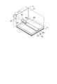
- FIG. 1 is a partial schematic perspective view of the coaxial microstrip line conversion circuit according to the first embodiment.
- 2A and 2B are a partial schematic perspective view and a schematic plan view of the housing portion.
- 3A and 3B are a schematic perspective view and a schematic plan view of the microstrip line substrate.
- the coaxial microstrip line conversion circuit 5 includes a housing portion 10, a microstrip line substrate 20, a coaxial line 30, and a solder layer 40.
- the housing portion 10 has a bottom surface 18 and a first side surface 14 provided with an opening 12.
- the bottom surface 18 has a projecting portion 16 that projects upward from the housing portion 10 and contacts the back surface of the microstrip line substrate 20.
- the thickness of the protruding portion 16 is T1.
- the housing portion 10 may be made of, for example, an aluminum alloy.
- FIG. 2B is a schematic plan view showing the upper surface of the protruding portion 16.
- the upper surface of the protrusion 16 has a substantially trapezoidal shape, and the protrusion 16 has a side surface 16t and a side surface 16s parallel to the first side surface 14.
- the side surface 16s connects the first side surface 14 and the side surface 16t.
- the side surface 16s is, for example, a curved surface having an R0.5 mm.
- the distance from the first side surface 14 to the side surface 16t is, for example, 0.6 mm.
- the length of the side surface 16t in the direction along the first side surface 14 is, for example, 0.8 mm.
- the coaxial line 30 is attached to the first side surface 14 and has a columnar central conductor portion 32 and an inner side surface facing the central conductor portion 32 and is concentric. It has a grounding conductor portion 34 arranged in a shape.
- One end 32a of the central conductor 32 extends from the opening 12 toward the inside of the housing 10.
- the microstrip line substrate 20 includes a dielectric 22, a microstrip line 24 provided on the upper surface of the dielectric 22, and a ground conductive portion 26 provided on the lower surface of the dielectric 22. And have. Let the thickness of the dielectric 22 be T2.
- the material of the dielectric 22 can be, for example, a low dielectric constant glass cloth.
- the microstrip line 24 and the ground conductive portion 26 can be made of, for example, Cu foil having a thickness of 20 ⁇ m.
- the solder layer 40 joins one end 32a of the central conductor portion 32 and one end of the microstrip line 24.
- the lower surface of the dielectric 22 is provided with a recess 28 in which a predetermined region adjacent to the protrusion 16 is cut, and a part of the ground conductive portion 26 is bent and provided on the cut surface.
- T3 be the thickness of the dielectric 22 in the thinned region.
- the microstrip line substrate 20 is fixed to the bottom surface 18 of the housing portion 10 with screws or the like so that the recess 28 and the protrusion 16 fit together.
- the line width W1 of the microstrip line 24 on the side opposite to the recess 28 is narrower than the line width W2 of the microstrip line 24 in the region of the dielectric 22 where the recess 28 is not provided.
- the line widths W1 and W2 can be determined so as to have a predetermined characteristic impedance (for example, 50 ⁇ ).
- FIG. 3B is a schematic plan view showing the recess 28.
- FIG. 3B shows a cross section parallel to the upper surface of the dielectric 22.
- the recess 28 has a side surface 28s and a side surface 28t.
- the side surface 28t is parallel to the outer surface of the dielectric 22, and the side surface 28s connects the outer surface of the dielectric 22 with the side surface 28t.
- the side surface 28s is, for example, a curved surface having an R0.5 mm.
- the recess 28 has an opening width of 1.4 mm, for example, in a direction parallel to the outer surface of the dielectric 22. Further, the recess 28 has a depth of 0.6 mm, for example, in a direction perpendicular to the outer surface of the dielectric 22.
- FIG. 4 is a schematic cross-sectional view taken along the line AA of the first embodiment.
- the lowest position 34a of the inner surface of the grounding conductor portion 34 facing the central conductor portion 32 and the grounding surface 26a of the grounding conductive portion 26 adjacent to the cutting surface is smaller than the vertical distance TG2 between the grounding surface 26b of the grounding conductive conductor 26 adjacent to the region of the lower surface of the dielectric 22 where the recess 28 is not provided and the lowest position 34a. ..
- the diameter of the central conductor portion 32 is d (mm), and the diameter of the inner surface of the ground conductor portion 34 is D (mm).
- the characteristic impedance Z 0 of the coaxial line 30 is represented by the equation (1).
- a hollow coaxial line having a relative permittivity ⁇ r 1, its characteristic impedance Z 0 is 50 ⁇ .
- the cutoff frequency f c of the coaxial line 30 is expressed by the equation (2).
- the vertical distance between the lowest position 34a in the vertical cross section of the grounding conductor portion 34 of the coaxial line 30 and the grounding surface 26a of the grounding conductive portion 26 of the microstrip line substrate 20 provided in the recess 28 By bringing TG1 closer, the discontinuity of the propagation mode is reduced.
- the thickness T2 of the microstrip line substrate 20 is thinned only in the vicinity of the connection position between the coaxial line 30 and the microstrip line substrate 20 to suppress the warp of the dielectric 22. That is, it becomes easy to make the distance between the central conductor portion 32 and the ground conductor portion 34 smaller than the thickness (0.4 mm) of the region where the recess 28 of the dielectric 22 is not provided.
- the thickness of the ground conductive portion 26 and the thickness of the microstrip line 24 are each ⁇ . Further, let ⁇ be the vertical distance between the lower end of the central conductor portion 32 and the striped conductive portion 24.
- the ground conductive portion 26 and the microstrip line 24 can include, for example, Cu foil.
- the vertical distance TG1 is not zero, for example, in the range of plus or minus 0.05 mm, the lowest position 34a of the grounding conductor portion 34 of the coaxial line 30 and the grounding surface of the grounding conductor portion 26 of the microstrip line substrate 20.
- the vertical distance TG1 with 26a can be reduced, and the distance between the grounding point PH and the grounding point PV can be reduced to 0.28 mm or the like. Therefore, the discontinuity of the propagation mode in the coaxial microstrip line conversion circuit can be suppressed.
- FIG. 5 is a graph showing the frequency characteristic characteristics of the voltage standing wave ratio of the coaxial microstrip conversion circuit according to the second specific example of the first embodiment by electromagnetic field simulation.
- the vertical axis is the voltage standing wave ratio (VSWR: Voltage Standing Wave Ratio), and the horizontal axis is the frequency (GHz).
- VSWR Voltage Standing Wave Ratio
- GHz frequency
- the microstrip line 24 is terminated with a 50 ⁇ load, and the load impedance seen from the coaxial circuit 30 is measured.
- the frequency is kept low up to 40 GHz and the voltage standing wave ratio VSWR is kept low up to about 1.08.
- FIG. 6A is a schematic perspective view of a coaxial microstrip line conversion circuit according to a comparative example
- FIG. 6B is a schematic perspective view of the housing portion thereof
- FIG. 6C is a schematic perspective view of the microstrip line substrate. The figure.
- the size and structure of the coaxial line 130 shall be the same as in the first embodiment.
- the microstrip line 120 is not provided with a recess on the back surface side, and the thickness of the dielectric 112 is 0.4 mm. Further, the microstrip line substrate 120 is attached to the surface of the bottom surface 118 of the flat housing portion 110.
- FIG. 7 is a schematic cross-sectional view taken along the line AA of the comparative example.
- the thickness of the ground conductive portion 126 and the thickness of the microstrip line 124 are represented by ⁇ , the value of which is 0.02 mm, and the vertical distance between the lower end of the central conductor portion 132 and the microstrip line 124 is ⁇ . It is represented by, and the value is 0.06 mm.
- the vertical distance TTG between the lowest position 134a of the grounding conductor portion 134 of the coaxial line 130 and the grounding surface 126c of the grounding conductor portion 126 of the microstrip line substrate 120 is 0.22 mm.
- the grounding point PV at the end of the lowest position 134a on the inner surface of the grounding conductor portion 134 of the coaxial line 130 and the grounding point PH at the end of the grounding conductive portion 126 (the side of the grounding point PV) of the microstrip line substrate The distance between them is 0.24 mm vertically downward, 0.2 mm horizontally, and 0.02 mm vertically upward, for a total of 0.46 mm. That is, while the distance between the central conductor portion 132 and the ground conductor portion 134 is 0.26 mm, the thickness of the dielectric substrate 120 is as large as 0.4 mm, so it is difficult to bring the vertical distance TTG close to zero. The distance between the ground contact point PV and PH is as large as 0.46 mm. Therefore, the discontinuity of the propagation mode becomes large in the vicinity of the connection region, and the reflection of the high frequency signal increases.
- FIG. 8 is a graph of frequency characteristics according to an electromagnetic field simulation of the voltage standing wave ratio of the coaxial microstrip line conversion circuit according to the comparative example.
- the voltage standing wave ratio VSWR is about 1.2 at 24 GHz and deteriorates to about 1.43 at 40 GHz.
- the protrusion 16 having a thickness T1 is provided and fitted with the microstrip line 20 provided with the recess 28.
- the vertical distance TG1 between the lowest position 34a of the grounding conductor portion 34 of the coaxial line 30 and the grounding surface 26a of the grounding conductor portion 26 of the microstrip line 20 can be brought close to zero.
- the ground surface 26a is larger than the lowest position 34a of the ground conductor portion 34 of the coaxial line 30. Move down. In this case, for example, if the thickness T2 of the dielectric 22 or the thinned thickness T3 is reduced, the increase in the thickness of the conductive layer can be canceled and the vertical distance TG1 can be kept small.
- a part of the coaxial line 30 may have an SMP compatible connector attached to the first side surface 14 of the housing portion 10.
- a coaxial microstrip line conversion circuit capable of reducing reflection of a high frequency signal at several GHz or higher is provided.
- This coaxial microstrip line conversion circuit can be widely used in communication equipment in the microwave band to the millimeter wave band.
Landscapes
- Waveguides (AREA)
- Coupling Device And Connection With Printed Circuit (AREA)
Priority Applications (3)
| Application Number | Priority Date | Filing Date | Title |
|---|---|---|---|
| JP2021529893A JP7397872B2 (ja) | 2019-07-03 | 2020-04-10 | 同軸マイクロストリップ線路変換回路 |
| US17/623,784 US12068520B2 (en) | 2019-07-03 | 2020-04-10 | Coaxial microstrip line conversion circuit |
| EP20834855.7A EP3996201B1 (en) | 2019-07-03 | 2020-04-10 | Coaxial microstrip line conversion circuit |
Applications Claiming Priority (2)
| Application Number | Priority Date | Filing Date | Title |
|---|---|---|---|
| JP2019-124371 | 2019-07-03 | ||
| JP2019124371 | 2019-07-03 |
Publications (1)
| Publication Number | Publication Date |
|---|---|
| WO2021002077A1 true WO2021002077A1 (ja) | 2021-01-07 |
Family
ID=74100661
Family Applications (1)
| Application Number | Title | Priority Date | Filing Date |
|---|---|---|---|
| PCT/JP2020/016086 Ceased WO2021002077A1 (ja) | 2019-07-03 | 2020-04-10 | 同軸マイクロストリップ線路変換回路 |
Country Status (4)
| Country | Link |
|---|---|
| US (1) | US12068520B2 (https=) |
| EP (1) | EP3996201B1 (https=) |
| JP (1) | JP7397872B2 (https=) |
| WO (1) | WO2021002077A1 (https=) |
Families Citing this family (1)
| Publication number | Priority date | Publication date | Assignee | Title |
|---|---|---|---|---|
| CN119518254B (zh) * | 2024-11-26 | 2025-10-28 | 上海师范大学 | 基于基片集成波导和基片集成同轴线的混合结构 |
Citations (5)
| Publication number | Priority date | Publication date | Assignee | Title |
|---|---|---|---|---|
| JPH01241201A (ja) * | 1988-03-22 | 1989-09-26 | Sharp Corp | 回路基板 |
| JPH05109452A (ja) * | 1991-10-14 | 1993-04-30 | Nissan Motor Co Ltd | 高周波用同軸型コネクタ |
| JPH05235613A (ja) * | 1991-08-29 | 1993-09-10 | Sanyo Electric Co Ltd | 同軸−マイクロストリップ変換コネクター構造 |
| JP2003068905A (ja) * | 2001-08-27 | 2003-03-07 | Kyocera Corp | 半導体素子収納用パッケージおよび半導体装置 |
| JP2010192987A (ja) | 2009-02-16 | 2010-09-02 | Nec Corp | 同軸コネクタ、同軸コネクタ・平面線路接続構造 |
Family Cites Families (51)
| Publication number | Priority date | Publication date | Assignee | Title |
|---|---|---|---|---|
| US3539966A (en) * | 1968-07-23 | 1970-11-10 | Us Army | Microwave connector |
| US4280112A (en) * | 1979-02-21 | 1981-07-21 | Eisenhart Robert L | Electrical coupler |
| US4463324A (en) * | 1982-06-03 | 1984-07-31 | Sperry Corporation | Miniature coaxial line to waveguide transition |
| JPS6032402A (ja) * | 1983-08-01 | 1985-02-19 | Matsushita Electric Ind Co Ltd | 同軸−ストリップライン変換装置 |
| JPS6113583A (ja) * | 1984-06-27 | 1986-01-21 | 日本電気株式会社 | 高周波コネクタ |
| US4816791A (en) * | 1987-11-27 | 1989-03-28 | General Electric Company | Stripline to stripline coaxial transition |
| US4837529A (en) * | 1988-03-24 | 1989-06-06 | Honeywell, Inc. | Millimeter wave microstrip to coaxial line side-launch transition |
| US4995815A (en) * | 1990-02-26 | 1991-02-26 | At&T Bell Laboratories | Coaxial transmission line to strip line coupler |
| US5198786A (en) * | 1991-12-04 | 1993-03-30 | Raytheon Company | Waveguide transition circuit |
| US5215477A (en) * | 1992-05-19 | 1993-06-01 | Alcatel Network Systems, Inc. | Variable location connector for communicating high frequency electrical signals |
| US5402088A (en) * | 1992-12-03 | 1995-03-28 | Ail Systems, Inc. | Apparatus for the interconnection of radio frequency (RF) monolithic microwave integrated circuits |
| US5418505A (en) * | 1993-07-26 | 1995-05-23 | E-Systems, Inc. | Coax-to-microstrip transition |
| US5886590A (en) * | 1997-09-04 | 1999-03-23 | Hughes Electronics Corporation | Microstrip to coax vertical launcher using fuzz button and solderless interconnects |
| US5982338A (en) * | 1997-12-08 | 1999-11-09 | Raytheon Company | Rectangular coaxial line to microstrip line matching transition and antenna subarray including the same |
| US5963111A (en) * | 1998-04-09 | 1999-10-05 | Raytheon Company | Orthogonal transition from coax to stripline for opposite sides of a stripline board |
| US6007347A (en) * | 1998-05-20 | 1999-12-28 | Tektronix, Inc. | Coaxial cable to microstrip connection and method |
| US6100774A (en) * | 1998-07-31 | 2000-08-08 | Raytheon Company | High uniformity microstrip to modified-square-ax interconnect |
| US6236287B1 (en) * | 1999-05-12 | 2001-05-22 | Raytheon Company | Wideband shielded coaxial to microstrip orthogonal launcher using distributed discontinuities |
| JP3976473B2 (ja) * | 2000-05-09 | 2007-09-19 | 日本電気株式会社 | 高周波回路及びそれを用いたモジュール、通信機 |
| SE520321C2 (sv) * | 2001-04-11 | 2003-06-24 | Allgon Ab | Kretskortskontakt |
| US6575762B2 (en) * | 2001-09-17 | 2003-06-10 | Fci Americas Technology, Inc. | Connection of coaxial cable to a circuit board |
| US6457979B1 (en) * | 2001-10-29 | 2002-10-01 | Agilent Technologies, Inc. | Shielded attachment of coaxial RF connector to thick film integrally shielded transmission line on a substrate |
| US6774742B1 (en) * | 2002-05-23 | 2004-08-10 | Applied Microcircuits Corporation | System and method for interfacing a coaxial connector to a coplanar waveguide substrate |
| US6894582B2 (en) * | 2003-02-07 | 2005-05-17 | Harris Corporation | Microwave device having a slotted coaxial cable-to-microstrip connection and related methods |
| JP4381701B2 (ja) * | 2003-03-13 | 2009-12-09 | 三菱電機株式会社 | 同軸コネクタと多層基板との接続構造 |
| JP2005317298A (ja) * | 2004-04-28 | 2005-11-10 | Hirose Electric Co Ltd | 同軸ケーブル用端子と、この同軸ケーブル用端子の取付構造及び取付方法 |
| TWI290443B (en) * | 2005-05-10 | 2007-11-21 | Via Tech Inc | Signal transmission structure, wire board and connector assembly structure |
| US7295084B2 (en) * | 2005-09-28 | 2007-11-13 | Agilent Technologies, Inc. | Electrical interconnection for coaxial line to slab line structure including a bead ring |
| US7500855B2 (en) * | 2006-10-30 | 2009-03-10 | Emerson Network Power Connectivity Solutions | Coaxial connector assembly with self-aligning, self-fixturing mounting terminals |
| CA2710940A1 (en) * | 2008-02-01 | 2009-08-13 | Raytheon Company | Radio frequency connector |
| US7750764B2 (en) * | 2008-02-27 | 2010-07-06 | Microsemi Corporation | Coaxial-to-microstrip transitions and manufacturing methods |
| US8035466B2 (en) * | 2009-01-12 | 2011-10-11 | Kenneth Ray Payne | High frequency electrical connector |
| JP5286190B2 (ja) * | 2009-08-03 | 2013-09-11 | 富士通コンポーネント株式会社 | 同軸コネクタ、及びコネクタ装置 |
| FR2950200A1 (fr) * | 2009-09-11 | 2011-03-18 | Thales Sa | Dispositif de raccordement pour signaux haute frequence entre un connecteur et une ligne de transmission |
| US8350638B2 (en) * | 2009-11-20 | 2013-01-08 | General Motors Llc | Connector assembly for providing capacitive coupling between a body and a coplanar waveguide and method of assembling |
| JP2011193151A (ja) * | 2010-03-12 | 2011-09-29 | Sony Corp | 高周波結合器並びに通信装置 |
| CN102208710B (zh) * | 2010-03-31 | 2014-11-19 | 安德鲁公司 | 射频同轴电缆至空气微带耦合接地转换结构及相应的天线 |
| US8384492B2 (en) * | 2010-09-07 | 2013-02-26 | National Taipei University Of Technology | Coaxial line to microstrip connector having slots in the microstrip line for receiving an encircling metallic plate |
| TW201216568A (en) * | 2010-10-08 | 2012-04-16 | Univ Nat Taipei Technology | Connector |
| US9054403B2 (en) * | 2012-06-21 | 2015-06-09 | Raytheon Company | Coaxial-to-stripline and stripline-to-stripline transitions including a shorted center via |
| US10211506B2 (en) * | 2013-02-12 | 2019-02-19 | Commscope Technologies Llc | Dual capacitively coupled coaxial cable to air microstrip transition |
| US9780431B2 (en) * | 2013-02-12 | 2017-10-03 | Commscope Technologies Llc | Dual capacitively coupled coaxial cable to air microstrip transition |
| CN103647127B (zh) * | 2013-12-09 | 2017-02-01 | 上海贝尔股份有限公司 | 用于将同轴电缆耦接至带状线的连接器 |
| FR3029702B1 (fr) * | 2014-12-03 | 2016-12-09 | Sagemcom Broadband Sas | Connecteur coaxial integre a un blindage et carte electronique equipee d'un tel connecteur |
| JP6143971B2 (ja) * | 2015-05-19 | 2017-06-07 | 三菱電機株式会社 | 同軸マイクロストリップ線路変換回路 |
| TWI560956B (en) * | 2016-06-07 | 2016-12-01 | Univ Nat Taipei Technology | Method to design and assemble a connector for the transition between a coaxial cable and a microstrip line |
| WO2018007580A1 (de) * | 2016-07-08 | 2018-01-11 | Hirschmann Car Communication Gmbh | Kabelmontage für koaxialkabel auf dicken leiterplatten |
| US10340233B1 (en) | 2016-12-06 | 2019-07-02 | Lockheed Martin Corporation | Millimeter wave connectors to integrated circuit interposer boards |
| EP3432424A1 (en) * | 2017-07-20 | 2019-01-23 | Spinner GmbH | Rf connector with a surface-mount interface |
| US10709011B2 (en) * | 2018-01-31 | 2020-07-07 | Raytheon Company | Radio frequency (RF) shielding structure for RF connector to microwave transmission interconnect regions and methods for manufacturing such RF shielding structure |
| TWI668909B (zh) * | 2018-05-02 | 2019-08-11 | National Taipei University Of Technology | 應用於同軸結構至微帶線之間的垂直轉接方法 |
-
2020
- 2020-04-10 US US17/623,784 patent/US12068520B2/en active Active
- 2020-04-10 EP EP20834855.7A patent/EP3996201B1/en active Active
- 2020-04-10 JP JP2021529893A patent/JP7397872B2/ja active Active
- 2020-04-10 WO PCT/JP2020/016086 patent/WO2021002077A1/ja not_active Ceased
Patent Citations (5)
| Publication number | Priority date | Publication date | Assignee | Title |
|---|---|---|---|---|
| JPH01241201A (ja) * | 1988-03-22 | 1989-09-26 | Sharp Corp | 回路基板 |
| JPH05235613A (ja) * | 1991-08-29 | 1993-09-10 | Sanyo Electric Co Ltd | 同軸−マイクロストリップ変換コネクター構造 |
| JPH05109452A (ja) * | 1991-10-14 | 1993-04-30 | Nissan Motor Co Ltd | 高周波用同軸型コネクタ |
| JP2003068905A (ja) * | 2001-08-27 | 2003-03-07 | Kyocera Corp | 半導体素子収納用パッケージおよび半導体装置 |
| JP2010192987A (ja) | 2009-02-16 | 2010-09-02 | Nec Corp | 同軸コネクタ、同軸コネクタ・平面線路接続構造 |
Non-Patent Citations (1)
| Title |
|---|
| See also references of EP3996201A4 |
Also Published As
| Publication number | Publication date |
|---|---|
| EP3996201A1 (en) | 2022-05-11 |
| US12068520B2 (en) | 2024-08-20 |
| JPWO2021002077A1 (https=) | 2021-01-07 |
| EP3996201A4 (en) | 2023-07-19 |
| US20220247060A1 (en) | 2022-08-04 |
| EP3996201B1 (en) | 2025-05-14 |
| JP7397872B2 (ja) | 2023-12-13 |
Similar Documents
| Publication | Publication Date | Title |
|---|---|---|
| US10418708B2 (en) | Wideband antenna | |
| US10008783B2 (en) | Patch antenna | |
| JP5431433B2 (ja) | 高周波線路−導波管変換器 | |
| CN1117414C (zh) | 微波传输带天线和包含所述天线的设备 | |
| US8502747B2 (en) | Dipole antenna assembly | |
| US20130171951A1 (en) | Extendable-arm antennas, and modules and systems in which they are incorporated | |
| CN104051440A (zh) | 具有天线的半导体结构 | |
| TWI663785B (zh) | 電子裝置、射頻裝置及其訊號傳輸構件 | |
| CN104409852A (zh) | 基于液晶材料的定频扫描漏波天线 | |
| US11240909B2 (en) | Antenna device | |
| JP6876942B2 (ja) | 回路基板 | |
| US9583836B2 (en) | High-frequency transmission line and antenna device | |
| US20150222003A1 (en) | Microwave circuit | |
| CN209571548U (zh) | 一种微带型isgw圆极化缝隙行波天线 | |
| WO2021002077A1 (ja) | 同軸マイクロストリップ線路変換回路 | |
| KR20180088002A (ko) | 전송선로-도파관 전이 장치 | |
| US20070040761A1 (en) | Method and apparatus for wideband omni-directional folded beverage antenna | |
| JP2005051330A (ja) | 誘電体導波管線路と高周波伝送線路との接続構造およびそれを用いた高周波回路基板ならびに高周波素子搭載用パッケージ | |
| CN110838616B (zh) | 集成基片间隙波导四臂圆极化天线 | |
| CN109950688B (zh) | 微带型isgw圆极化缝隙行波天线 | |
| US12519070B2 (en) | System, electronic device and package with vertical to horizontal substrate integrated waveguide transition and horizontal grounded coplanar waveguide transition | |
| US20140043190A1 (en) | Planar inverted f antenna structure | |
| JP3347640B2 (ja) | 高周波用伝送線路 | |
| KR102111143B1 (ko) | 반도체 온-칩 안테나 | |
| EP3449703A1 (en) | Radiofrequency structures in electronic packages |
Legal Events
| Date | Code | Title | Description |
|---|---|---|---|
| 121 | Ep: the epo has been informed by wipo that ep was designated in this application |
Ref document number: 20834855 Country of ref document: EP Kind code of ref document: A1 |
|
| DPE1 | Request for preliminary examination filed after expiration of 19th month from priority date (pct application filed from 20040101) | ||
| ENP | Entry into the national phase |
Ref document number: 2021529893 Country of ref document: JP Kind code of ref document: A |
|
| NENP | Non-entry into the national phase |
Ref country code: DE |
|
| ENP | Entry into the national phase |
Ref document number: 2020834855 Country of ref document: EP Effective date: 20220203 |
|
| WWG | Wipo information: grant in national office |
Ref document number: 2020834855 Country of ref document: EP |