US11240909B2 - Antenna device - Google Patents
Antenna device Download PDFInfo
- Publication number
- US11240909B2 US11240909B2 US16/711,654 US201916711654A US11240909B2 US 11240909 B2 US11240909 B2 US 11240909B2 US 201916711654 A US201916711654 A US 201916711654A US 11240909 B2 US11240909 B2 US 11240909B2
- Authority
- US
- United States
- Prior art keywords
- conductor
- antenna
- ground conductor
- antenna device
- ground
- Prior art date
- Legal status (The legal status is an assumption and is not a legal conclusion. Google has not performed a legal analysis and makes no representation as to the accuracy of the status listed.)
- Expired - Fee Related, expires
Links
Images


Classifications
-
- H—ELECTRICITY
- H01—ELECTRIC ELEMENTS
- H01Q—ANTENNAS, i.e. RADIO AERIALS
- H01Q9/00—Electrically-short antennas having dimensions not more than twice the operating wavelength and consisting of conductive active radiating elements
- H01Q9/04—Resonant antennas
- H01Q9/06—Details
- H01Q9/065—Microstrip dipole antennas
-
- H—ELECTRICITY
- H05—ELECTRIC TECHNIQUES NOT OTHERWISE PROVIDED FOR
- H05K—PRINTED CIRCUITS; CASINGS OR CONSTRUCTIONAL DETAILS OF ELECTRIC APPARATUS; MANUFACTURE OF ASSEMBLAGES OF ELECTRICAL COMPONENTS
- H05K1/00—Printed circuits
- H05K1/02—Details
- H05K1/0213—Electrical arrangements not otherwise provided for
- H05K1/0237—High frequency adaptations
- H05K1/0243—Printed circuits associated with mounted high frequency components
-
- H—ELECTRICITY
- H01—ELECTRIC ELEMENTS
- H01Q—ANTENNAS, i.e. RADIO AERIALS
- H01Q1/00—Details of, or arrangements associated with, antennas
- H01Q1/48—Earthing means; Earth screens; Counterpoises
-
- H—ELECTRICITY
- H01—ELECTRIC ELEMENTS
- H01Q—ANTENNAS, i.e. RADIO AERIALS
- H01Q15/00—Devices for reflection, refraction, diffraction or polarisation of waves radiated from an antenna, e.g. quasi-optical devices
- H01Q15/0006—Devices acting selectively as reflecting surface, as diffracting or as refracting device, e.g. frequency filtering or angular spatial filtering devices
- H01Q15/006—Selective devices having photonic band gap materials or materials of which the material properties are frequency dependent, e.g. perforated substrates, high-impedance surfaces
-
- H—ELECTRICITY
- H01—ELECTRIC ELEMENTS
- H01Q—ANTENNAS, i.e. RADIO AERIALS
- H01Q5/00—Arrangements for simultaneous operation of antennas on two or more different wavebands, e.g. dual-band or multi-band arrangements
- H01Q5/30—Arrangements for providing operation on different wavebands
- H01Q5/378—Combination of fed elements with parasitic elements
-
- H—ELECTRICITY
- H01—ELECTRIC ELEMENTS
- H01Q—ANTENNAS, i.e. RADIO AERIALS
- H01Q9/00—Electrically-short antennas having dimensions not more than twice the operating wavelength and consisting of conductive active radiating elements
- H01Q9/04—Resonant antennas
- H01Q9/0407—Substantially flat resonant element parallel to ground plane, e.g. patch antenna
- H01Q9/045—Substantially flat resonant element parallel to ground plane, e.g. patch antenna with particular feeding means
-
- H—ELECTRICITY
- H05—ELECTRIC TECHNIQUES NOT OTHERWISE PROVIDED FOR
- H05K—PRINTED CIRCUITS; CASINGS OR CONSTRUCTIONAL DETAILS OF ELECTRIC APPARATUS; MANUFACTURE OF ASSEMBLAGES OF ELECTRICAL COMPONENTS
- H05K1/00—Printed circuits
- H05K1/02—Details
- H05K1/0213—Electrical arrangements not otherwise provided for
- H05K1/0237—High frequency adaptations
- H05K1/025—Impedance arrangements, e.g. impedance matching, reduction of parasitic impedance
- H05K1/0253—Impedance adaptations of transmission lines by special lay-out of power planes, e.g. providing openings
-
- H—ELECTRICITY
- H05—ELECTRIC TECHNIQUES NOT OTHERWISE PROVIDED FOR
- H05K—PRINTED CIRCUITS; CASINGS OR CONSTRUCTIONAL DETAILS OF ELECTRIC APPARATUS; MANUFACTURE OF ASSEMBLAGES OF ELECTRICAL COMPONENTS
- H05K1/00—Printed circuits
- H05K1/02—Details
- H05K1/0296—Conductive pattern lay-out details not covered by sub groups H05K1/02 - H05K1/0295
- H05K1/0298—Multilayer circuits
-
- H—ELECTRICITY
- H05—ELECTRIC TECHNIQUES NOT OTHERWISE PROVIDED FOR
- H05K—PRINTED CIRCUITS; CASINGS OR CONSTRUCTIONAL DETAILS OF ELECTRIC APPARATUS; MANUFACTURE OF ASSEMBLAGES OF ELECTRICAL COMPONENTS
- H05K1/00—Printed circuits
- H05K1/16—Printed circuits incorporating printed electric components, e.g. printed resistors, capacitors or inductors
- H05K1/165—Printed circuits incorporating printed electric components, e.g. printed resistors, capacitors or inductors incorporating printed inductors
-
- H—ELECTRICITY
- H05—ELECTRIC TECHNIQUES NOT OTHERWISE PROVIDED FOR
- H05K—PRINTED CIRCUITS; CASINGS OR CONSTRUCTIONAL DETAILS OF ELECTRIC APPARATUS; MANUFACTURE OF ASSEMBLAGES OF ELECTRICAL COMPONENTS
- H05K2201/00—Indexing scheme relating to printed circuits covered by H05K1/00
- H05K2201/10—Details of components or other objects attached to or integrated in a printed circuit board
- H05K2201/10007—Types of components
- H05K2201/10098—Components for radio transmission, e.g. radio frequency identification [RFID] tag, printed or non-printed antennas
Definitions
- the present disclosure relates to an antenna device.
- Patent Literature 1 discloses an antenna device that includes an artificial magnetic conductor.
- PTL 1 is Unexamined Japanese Patent Publication No. 2015-70542.
- An object of the present disclosure is to provide an antenna device that achieves a wider band of a communication frequency and compactness while maintaining a frequency characteristic of a fundamental wave.
- the present disclosure is an antenna device that includes an antenna, a first ground conductor, and an artificial magnetic conductor that is sandwiched between the antenna and the first ground conductor, and separated from the antenna and the first ground conductor.
- the first ground conductor includes a first cutaway part on end side, the first cutaway part having a substantially rectangular shape.
- the present disclosure achieves a wider band of a communication frequency and compactness of an antenna device while maintaining a frequency characteristic of a fundamental wave.
- FIG. 1 is an external perspective view of an antenna device according to an exemplary embodiment
- FIG. 2 is a vertical cross-sectional view taken along a line 2 - 2 of FIG. 1 ;
- FIG. 3 is a perspective view illustrating an antenna surface, an AMC surface, and a ground surface that are included in a plurality of layers constituting the antenna device;
- FIG. 4 is a plan view of the antenna surface that is a surface of a printed wiring board in the antenna device, an antenna conductor and a passive conductor being formed on the surface of the printed wiring board;
- FIG. 5 is a plan view of the AMC surface in the antenna device, omitting layers upper than an AMC;
- FIG. 6 is a plan view of the ground surface in the antenna device, omitting layers upper than a ground conductor;
- FIG. 7 is a directivity characteristic diagram illustrating an example of a radio wave radiation pattern in parallel resonance.
- FIG. 8 is a graph illustrating a characteristic example of a voltage standing wave ratio of the antenna device.
- present exemplary embodiment in which a configuration and an operation of an antenna device according to the present disclosure are specifically disclosed will be described in detail with reference to the drawings as appropriate. However, in some cases, an unnecessarily detailed description may be omitted. For example, a detailed description of a well-known matter and a duplicated description of substantially the same configuration will be omitted in some cases. This is to avoid unnecessary redundancy in the following description and to facilitate understanding by those skilled in the art.
- the accompanying drawings and the following description are provided to enable those skilled in the art to sufficiently understand the present disclosure, and are not intended to limit the subject matter described in the claims.
- the antenna device is included in a main phone or an extension of a cordless telephone unit that uses a digital enhanced cordless telecommunications (DECT) system with a frequency band of 1.9 GHz, for example.
- the antenna device is used for not only the main phone or the extension of the cordless telephone unit described above but also many Internet of Things (IoT) devices such as a display unit of a television device, a seat monitor in an airplane, an electronic shelf label (for example, card-type electronic device that is attached to shelf in retail store and displays selling price of product), a smart speaker, an in-vehicle device, a microwave oven, and a refrigerator.
- IoT Internet of Things
- the present exemplary embodiment will describe a dipole antenna as an example of the antenna device.
- the description is applicable to a monopole antenna.
- the dipole antenna is formed by, for example, etching a metal foil on a printed wiring board that is a multilayer circuit board including a plurality of layers.
- the printed wiring board is constituted by a plurality of layers such as copper foil and glass epoxy.
- FIG. 1 is an external perspective view of antenna device 101 according to the present exemplary embodiment.
- FIG. 2 is a vertical cross-sectional view taken along a line 2 - 2 of FIG. 1 .
- FIG. 3 is a perspective view illustrating an antenna surface, an artificial magnetic conductor (AMC) surface, and a ground surface that are included in a plurality of layers constituting antenna device 101 .
- FIG. 4 is a plan view of the antenna surface that is surface 1 a of printed wiring board 1 in antenna device 101 , antenna conductors 2 , 3 and passive conductor 6 being formed on surface 1 a of printed wiring board 1 .
- FIG. 5 is a plan view of the AMC surface in antenna device 101 , omitting layers upper than AMC 7 (layers in +x direction).
- FIG. 6 is a plan view of the ground surface in antenna device 101 , omitting layers upper than ground conductor 8 .
- antenna device 101 includes printed wiring board 1 , antenna conductor 2 that is a strip conductor as an example of a feed antenna, antenna conductor 3 that is a strip conductor as an example of a parasitic antenna, and passive conductor 6 disposed on sides of antenna conductors 2 , 3 .
- Passive conductor 6 is electrically separated from antenna conductors 2 , 3 .
- Antenna conductors 2 , 3 are connected respectively to via conductors 4 , 5 in printed wiring board 1 .
- Via conductor 4 constitutes a feed wire between feedpoint Q 1 of antenna conductor 2 and a wireless communication circuit (not illustrated).
- the wireless communication circuit is mounted on back surface 1 b of printed wiring board 1 , for example.
- Via conductor 5 constitutes a ground wire between feedpoint Q 2 of antenna conductor 3 and the wireless communication circuit described above.
- Antenna conductors 2 , 3 (sometimes collectively referred to as “antenna”) constitute a dipole antenna, extending longitudinally on a straight line toward a positive side and a negative side in a z-direction.
- the dipole antenna is formed on front surface 1 a of printed wiring board 1 such that ends of antenna conductors 2 , 3 adjacent to feedpoints Q 1 , Q 2 (hereinafter referred to as “feeder-side ends”) are separated from each other at a predetermined distance.
- Ends opposite the feeder-side ends of antenna conductors 2 , 3 are hereinafter referred to as “distal-side ends” of antenna conductors 2 , 3 .
- Passive conductor 6 is disposed adjacently to antenna conductors 2 , 3 with a predetermined distance between passive conductor 6 and antenna conductors 2 , 3 .
- the predetermined distance is within a quarter of a received wave wavelength, for example.
- Passive conductor 6 is disposed on one side surface side of antenna conductor 2 , 3 so as to be in parallel to a direction that antenna conductors 2 , 3 are arranged (that is to say, positive side and negative side in z-direction).
- passive conductor 6 can increase electrostatic capacitance between antenna conductors 2 , 3 and AMC 7 and shift a wireless frequency handled by antenna device 101 to a lower frequency band.
- a size and shape of passive conductor 6 and a number of passive conductors 6 are not particularly limited. If passive conductor 6 is disposed on a same side of AMC 7 as antenna conductors 2 , 3 and electrostatically coupled to AMC 7 , passive conductor 6 may be disposed on a same surface as AMC 7 , as well as on a same surface as a surface on which antenna conductors 2 , 3 are arranged.
- via conductors 4 , 5 are formed by filling conductors in through-holes or via holes that are formed from front surface 1 a to back surface 1 b of printed wiring board 1 in a thickness direction.
- Antenna conductor 2 is connected to a power feed terminal of the wireless communication circuit (described above) on back surface 1 b of printed wiring board 1 through via conductor 4 to function as a feed antenna.
- Antenna conductor 3 is connected to AMC 7 and ground conductors 8 in printed wiring board 1 and a ground terminal of the wireless communication circuit (described above) through via conductor 5 to function as a parasitic antenna.
- the z-axis direction represents a longitudinal direction of antenna device 101 and antenna conductors 2 , 3 of the antenna device.
- a y-axis direction represents a width direction of antenna device 101 and antenna conductors 2 , 3 of the antenna device and is orthogonal to the z-axis direction.
- An x-axis direction represents a thickness direction of antenna device 101 and is orthogonal to an xy-plane.
- via conductors 4 , 5 are formed at positions that are directly below respective feedpoints Q 1 , Q 2 and that substantially oppose to each other.
- Printed wiring board 1 of antenna device 101 may be mounted on a printed wiring board in an electronic device, for example.
- printed wiring board 1 that is a multilayer circuit board includes dielectric substrate 10 , AMC 7 , dielectric substrate 11 , ground conductor 8 , and dielectric substrate 12 that are stacked in this order.
- Dielectric substrates 10 , 11 , 12 are, for example, made of a material such as glass epoxy.
- AMC 7 is an artificial magnetic conductor that has perfect magnetic conductor (PMC) properties, and is formed of a predetermined metallic pattern. Use of AMC 7 enables the antenna device to achieve a reduction in thickness and an increase in gain.
- Via conductor 4 is a feeder wire that has, for example, a cylindrical shape and is used to supply electric power for driving antenna conductor 2 as an antenna, and electrically connects antenna conductor 2 formed on front surface 1 a of printed wiring board 1 to the power feed terminal of the wireless communication circuit (described above).
- Via conductor 4 is formed to be substantially coaxial with via conductor insulating holes 17 , 18 that are respectively formed in AMC 7 and ground conductor 8 so as not to be electrically connected to AMC 7 and ground conductor 8 (see FIG. 3 ).
- a diameter of via conductor 4 is less than a diameter of via conductor insulating holes 17 , 18 (see FIG. 2 ).
- antenna conductor 2 electrically connects antenna conductor 3 to the ground terminal of the wireless communication circuit (described above). Via conductor 5 is electrically connected to ground conductor 8 and AMC 7 (see FIG. 3 ).
- a surface on which antenna conductors 2 , 3 are mounted (specifically, surface on dielectric substrate 10 ) is referred to as “surface A” for convenience
- AMC 7 is referred to as “surface B” for convenience
- ground conductor 8 is referred to as “surface C” for convenience.
- antenna conductor 2 is not connected to (that is, not conducted with) surface B and surface C
- antenna conductor 3 is connected to (that is, conducted with) surface A, surface B, and surface C.
- antenna conductor 3 does not need to be connected to surface B.
- AMC 7 includes slit 71 at a center part in the z-axis direction. Slit 71 penetrates AMC 7 in the thickness direction and extends to a vicinity of ends of AMC 7 in the width direction.
- AMC 7 also includes cutaway part 7 c (one aspect of opening) that extends from a position separated from slit 71 at a predetermined distance in the longitudinal direction (that is to say, z-direction) to a left end of printed wiring board 1 (see FIG. 3 ). Cutaway part 7 c is formed in a rectangular shape with a predetermined width in the width direction.
- the artificial magnetic conductor is not formed in cutaway part 7 c and slit 71 on a layer of AMC 7 (see surface B in FIG. 3 ).
- Slit 71 separates AMC 7 at antenna conductors 2 , 3 to increase electrostatic coupling of antenna conductor 2 and a left side part of AMC 7 (that is to say, positive side in z-direction in FIG. 3 ) and electrostatic coupling of antenna conductor 3 and a right side part of AMC 7 (that is to say, negative side in z-direction in FIG. 3 ).
- Slit 71 may be formed to ends of AMC 7 in the width direction so as to completely separate AMC 7 into two pieces.
- Ground conductor 8 A is formed within cutaway part 7 c .
- Ground conductor 8 A is formed in a rectangular shape so as to be flush with AMC 7 along an inner periphery of cutaway part 7 c with a clearance from an inner wall of cutaway part 7 c .
- a hole is formed in ground conductor 8 A so as to be electrically connected to one end of via conductor 31 .
- a hole is formed in ground conductor 8 so as to be electrically connected to the other end of via conductor 31 .
- Ground conductor 8 A is conducted through via conductor 31 with ground conductor 8 (see FIGS. 2 and 3 ). As described above, the layer of AMC 7 (see surface B of FIG.
- ground conductor 8 A another ground layer that is, ground conductor 8 A
- ground layer a layer of ground conductor 8 (ground layer, see surface C of FIG. 3 ). Consequently, it is possible to effectively secure an apparent area of the ground layer and thus to ensure performance of antenna device 101 .
- Ground conductor 8 is an earth region that is connected to the ground terminal of the wireless communication circuit (described above). Cutaway part 8 z is formed at an end of ground conductor 8 in the longitudinal direction (that is to say, z-direction) (see FIGS. 2 and 3 ). Cutaway part 8 z is formed in a rectangular shape with a predetermined width to extend from a position separated from a center part of ground conductor 8 at a predetermined distance in the longitudinal direction (that is to say, z-direction) to a left end of ground conductor 8 .
- cutaway part 8 z is disposed on one end side of ground conductor 8 opposite to a position where via conductor 5 is disposed with a center of printed wiring board 1 being provided between cutaway part 8 z and the position where via conductor 5 is disposed (that is to say, side of via conductor 4 illustrated in FIG. 2 ).
- cutaway part 8 z is formed at one end side of ground conductor 8 opposite to via conductor 5 , a length of an entire periphery of ground conductor 8 (that is, electrical length that represents path length of alternating current flowing in antenna device 101 ) increases.
- a wireless frequency band handled by antenna device 101 can be widened as compared to a case where cutaway part 8 z is not formed.
- cutaway part 8 z is formed at a position of ground conductor 8 in the width direction in the present exemplary embodiment, cutaway part 8 z may be formed at a plurality of positions in the width direction.
- a shape of cutaway part 8 z is not limited to a rectangular shape. Cutaway part 8 z may have a polygonal shape or any shape with projections and recesses so as to increase the electrical length.
- Ground conductor 8 includes via conductor insulating hole 18 that is formed so as to cause via conductor 4 to penetrate ground conductor 8 and be electrically insulated from ground conductor 8 and a hole that is formed so as to cause via conductor 5 to penetrate ground conductor 8 and be electrically connected to ground conductor 8 .
- Ground conductor 8 also includes a hole that is formed so as to cause via conductor 31 to penetrate ground conductor 8 and be electrically connected to ground conductor 8 A.
- a planar shape of AMC 7 and a planar shape of ground conductor 8 are a substantially same rectangular shape and are substantially congruent.
- AMC 7 and ground conductor 8 are formed to oppose and overlap each other at a predetermined distance in the thickness direction.
- One of AMC 7 and ground conductor 8 does not project from another one and thus compactness of printed wiring board 1 can be achieved. This leads to compactness of antenna device 101 .
- AMC 7 has cutaway part 7 c and slit 71
- a length of AMC 7 in the longitudinal direction is substantially equal to a length of ground conductor 8 in the longitudinal direction.
- a configuration of the antenna device according to the comparative example is similar to the configuration of antenna device 101 except that ground conductor 8 does not have cutaway part 8 z , AMC 7 does not have cutaway part 7 c , and ground conductor 8 A is not disposed within cutaway part 7 c.
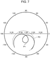
- FIG. 7 is a directivity characteristic diagram illustrating an example of a radio wave radiation pattern in parallel resonance.
- a center has a highest degree of impedance matching (maximum reflection coefficient 1 ).
- Radio wave radiation pattern P 1 of antenna device 101 according to the present exemplary embodiment approaches the center of the directivity characteristic diagram, then separates temporarily from the center, and approaches the center again. That is, radio wave radiation pattern P 1 has two curves approaching the center. Consequently, impedance matching occurs with high possibility and parallel resonance easily occurs.
- radio wave radiation pattern P 2 of the antenna device according to the comparative example (broken line in FIG.
- radio wave radiation pattern P 1 of antenna device 101 according to the present exemplary embodiment is placed near the center of the directivity characteristic diagram, a wider band can be achieved as compared to the antenna device according to the comparative example.
- FIG. 8 is a graph illustrating a characteristic example of a voltage standing wave ratio (VSWR) of antenna device 101 .
- a vertical axis represents a VSWR and a horizontal axis represents a frequency.
- the voltage standing wave ratio represents the degree of impedance matching (that is to say, degree of reflection) by a rate of a traveling wave and a reflected wave in a standing wave.
- the voltage standing wave ratio is calculated using a rate of a maximum amplitude and a minimum amplitude of voltage of a radio wave that is a standing wave.
- the VSWR is closer to 1, there are less reflected waves and impedance matching is achieved. Consequently, as the VSWR is closer to 1, radio wave transmission efficiency becomes higher.
- a frequency band with a VSWR of 3.0 or less is determined as a fractional bandwidth, and whether a frequency band is a wide band or a narrow band is determined by the fractional bandwidth.
- the fractional bandwidth is calculated by dividing a bandwidth with a VSWR of 3.0 or less by a center frequency.
- fH and fL denote respectively a maximum frequency and a minimum frequency of the bandwidth with a VSWR of 3.0 or less in antenna device 101 .
- FIG. 8 illustrates the fractional bandwidth in a frequency band near 1.9 GHz, for example.
- a frequency range with a VSWR of 3.0 or less ranges from 1.86 GHz to 2.03 GHz in antenna device 101 , as indicated by graph g 1 .
- the VSWR is the lowest at a frequency of 1.91 GHz.
- the frequency range with a VSWR of 3.0 or less ranges from 1.86 GHz to 1.97 GHz in the antenna device according to the comparative example, as indicated by graph g 2 .
- the VSWR is the lowest at a frequency of 1.91 GHz.
- cutaway part 8 z formed in ground conductor 8 and ground conductor 8 A disposed within cutaway part 7 c of AMC 7 contribute greatly to a wider band of antenna device 101 .
- antenna device 101 can transmit and receive wireless signals in a fundamental wave band, prevent radiation of wireless signals in a second harmonic band, and reduce influence of higher harmonics.
- cutaway part 8 z is formed in ground conductor 8 in printed wiring board 1 and ground conductor 8 A is formed within cutaway part 7 c of AMC 7 to be flush with AMC 7 in antenna device 101 , the electrical length can be increased without increasing the longitudinal length of ground conductor 8 . Consequently, it is possible to achieve a wider band of a wireless frequency of antenna device 101 and compactness of printed wiring board 1 including ground conductor 8 . As a result, antenna device 101 is easily incorporated in more devices and thus has a wide range of use.
- antenna device 101 includes antenna conductors 2 , 3 , ground conductor 8 (one aspect of first ground conductor), and artificial magnetic conductor 7 that is sandwiched between antenna conductors 2 , 3 and ground conductor 8 so as to be disposed separately from antenna conductors 2 , 3 and ground conductor 8 .
- Ground conductor 8 includes cutaway part 8 z (one aspect of first cutaway part) that has a rectangular shape on one end side. As cutaway part 8 z is formed in ground conductor 8 , the length of the entire periphery of ground conductor 8 (that is, electrical length that represents path length of alternating current flowing in antenna device 101 ) increases.
- antenna device 101 can thus be widened as compared to the case where cutaway part 8 z is not formed. Consequently, antenna device 101 can achieve a wider band of a communication frequency and compactness of an antenna device while maintaining a frequency characteristic of a fundamental wave.
- Antenna device 101 further includes via conductor 5 that is disposed separately from the center of printed wiring board 1 , having a substantially rectangular shape, on which antenna conductor 3 is disposed and that causes antenna conductor 3 , AMC 7 , and ground conductor 8 to be conducted with each other.
- Cutaway part 8 z is disposed on one end side of ground conductor 8 opposite to the position where via conductor 5 is disposed with the center of printed wiring board 1 being provided between cutaway part 8 z and the position where via conductor 5 is disposed. As cutaway part 8 z is formed on one end side of ground conductor 8 opposite to via conductor 5 in antenna device 101 , a wider band is achieved.
- Antenna device 101 also includes ground conductor 8 A (one aspect of second ground conductor) that is conducted with ground conductor 8 .
- AMC 7 includes cutaway part 7 c (one aspect of second cutaway part) that has a substantially same area as cutaway part 8 z in ground conductor 8 at a position substantially opposing cutaway part 8 z in ground conductor 8 .
- Ground conductor 8 A is disposed in cutaway part 7 c to be separated from AMC 7 .
- an AMC layer includes another ground layer that is conducted with a ground layer in antenna device 101 , the apparent area of the ground layer is secured, so that the performance of the antenna device is ensured.
- Antenna device 101 further includes passive conductor 6 that is disposed on printed wiring board 1 on which antenna conductors 2 , 3 are disposed.
- passive conductor 6 is electrostatically couple to AMC 7 similarly to antenna conductors 2 , 3 , passive conductor 6 can increase electrostatic capacitance between antenna conductors 2 , 3 and AMC 7 and shift a wireless frequency to a lower frequency band. That is, a peak of the VSWR can be shifted to a lower frequency band.
- Ground conductor 8 and AMC 7 are disposed to oppose and substantially overlap each other in a plan view.
- One of AMC 7 and ground conductor 8 does not project from another one and thus compactness can be achieved. This leads to compactness of antenna device 101 .
- the antenna includes antenna conductor 2 (one aspect of first antenna conductor) having feedpoint Q 1 (one aspect of first feedpoint) and antenna conductor 3 (one aspect of second antenna conductor) having feedpoint Q 2 (one aspect of second feedpoint), antenna conductor 3 being connected via conductor 5 to ground conductor 8 , thus configuring a dipole antenna.
- antenna conductor 2 one aspect of first antenna conductor
- antenna conductor 3 one aspect of second antenna conductor
- feedpoint Q 2 one aspect of second feedpoint
- AMC 7 includes slit 71 that separates antenna conductor 2 and antenna conductor 3 that are formed on an upper layer from each other. Consequently, slit 71 separates AMC 7 at antenna conductors 2 , 3 to increase electrostatic coupling of antenna conductor 2 and the left side part of AMC 7 (+z-direction) and electrostatic coupling of antenna conductor 3 and the right side part of AMC 7 ( ⁇ z-direction).
- the feeder-side end of antenna conductor 2 on a side of via conductor 4 is disposed to be shifted to the z-direction side with respect to the center of printed wiring board 1 of antenna device 101 . That is to say, according to antenna device 101 of the present exemplary embodiment, antenna conductors 2 , 3 and passive conductor 6 are not disposed at the center of printed wiring board 1 . As compared to a configuration in which antenna conductors 2 , 3 and passive conductor 6 are disposed at the center of printed wiring board 1 , it can be said that a part of printed wiring board 1 on the opposite side to a side at which cutaway part 8 z is disposed in ground conductor 8 is substantially cut.
- the present disclosure is useful because the present disclosure achieves a wider band of a communication frequency and compactness of an antenna device while maintaining a frequency characteristic of a fundamental wave.
Landscapes
- Engineering & Computer Science (AREA)
- Microelectronics & Electronic Packaging (AREA)
- Physics & Mathematics (AREA)
- Optics & Photonics (AREA)
- Details Of Aerials (AREA)
- Aerials With Secondary Devices (AREA)
- Waveguide Aerials (AREA)
Abstract
Description
Claims (7)
Applications Claiming Priority (3)
| Application Number | Priority Date | Filing Date | Title |
|---|---|---|---|
| JP2018235812A JP7122523B2 (en) | 2018-12-17 | 2018-12-17 | antenna device |
| JPJP2018-235812 | 2018-12-17 | ||
| JP2018-235812 | 2018-12-17 |
Publications (2)
| Publication Number | Publication Date |
|---|---|
| US20200196439A1 US20200196439A1 (en) | 2020-06-18 |
| US11240909B2 true US11240909B2 (en) | 2022-02-01 |
Family
ID=71071009
Family Applications (1)
| Application Number | Title | Priority Date | Filing Date |
|---|---|---|---|
| US16/711,654 Expired - Fee Related US11240909B2 (en) | 2018-12-17 | 2019-12-12 | Antenna device |
Country Status (2)
| Country | Link |
|---|---|
| US (1) | US11240909B2 (en) |
| JP (1) | JP7122523B2 (en) |
Families Citing this family (5)
| Publication number | Priority date | Publication date | Assignee | Title |
|---|---|---|---|---|
| JP7182134B2 (en) * | 2020-04-24 | 2022-12-02 | パナソニックIpマネジメント株式会社 | antenna device |
| JP7182137B2 (en) * | 2020-07-31 | 2022-12-02 | パナソニックIpマネジメント株式会社 | Antenna device and communication device |
| WO2022190876A1 (en) * | 2021-03-08 | 2022-09-15 | 株式会社ヨコオ | Antenna |
| WO2023024023A1 (en) * | 2021-08-26 | 2023-03-02 | 京东方科技集团股份有限公司 | Antenna structure and electronic device |
| JP2023180978A (en) * | 2022-06-10 | 2023-12-21 | パナソニックIpマネジメント株式会社 | Antenna equipment and communication equipment |
Citations (15)
| Publication number | Priority date | Publication date | Assignee | Title |
|---|---|---|---|---|
| US20030231142A1 (en) * | 2002-06-14 | 2003-12-18 | Mckinzie William E. | Multiband artificial magnetic conductor |
| US20060092079A1 (en) * | 2004-10-01 | 2006-05-04 | De Rochemont L P | Ceramic antenna module and methods of manufacture thereof |
| US20070285318A1 (en) * | 2006-06-09 | 2007-12-13 | Sony Ericsson Mobile Communications Ab | Use of amc materials in relation to antennas of a portable communication device |
| US20110156972A1 (en) * | 2009-12-29 | 2011-06-30 | Heikki Korva | Loop resonator apparatus and methods for enhanced field control |
| US20120256811A1 (en) * | 2011-04-07 | 2012-10-11 | Hrl Laboratories, Llc | Widebrand Adaptable Artificial Impedance Surface |
| US20130249752A1 (en) * | 2010-04-11 | 2013-09-26 | Broadcom Corporation | Three-Dimensional Multiple Spiral Antenna and Applications Thereof |
| US20140203993A1 (en) * | 2011-08-24 | 2014-07-24 | Nec Corporation | Antenna and electronic device |
| US20140225795A1 (en) * | 2013-02-08 | 2014-08-14 | Sj Antenna Design | Shielding module integrating antenna and integrated circuit component |
| JP2015070542A (en) | 2013-09-30 | 2015-04-13 | マスプロ電工株式会社 | Antenna device |
| US20170033468A1 (en) * | 2014-04-18 | 2017-02-02 | Transsip, Inc. | Metamaterial Substrate For Circuit Design |
| US20170033435A1 (en) * | 2014-04-23 | 2017-02-02 | Murata Manufacturing Co., Ltd. | Antenna device and electronic appliance |
| US20170187229A1 (en) * | 2015-12-24 | 2017-06-29 | Energous Corporation | Ceramic antenna molds |
| US20190098750A1 (en) * | 2017-09-27 | 2019-03-28 | Lg Electronics Inc. | Electronic device |
| US20190393603A1 (en) * | 2017-02-27 | 2019-12-26 | Proant Ab | Antenna Arrangement And A Device Comprising Such An Antenna Arrangement |
| US20210273319A1 (en) * | 2018-05-17 | 2021-09-02 | South China University Of Technology | Filtering antenna for wearable apparatus |
Family Cites Families (2)
| Publication number | Priority date | Publication date | Assignee | Title |
|---|---|---|---|---|
| JP5065951B2 (en) | 2008-03-11 | 2012-11-07 | Necトーキン株式会社 | Impedance matching method in antenna device and antenna device |
| WO2017038045A1 (en) | 2015-08-31 | 2017-03-09 | パナソニックIpマネジメント株式会社 | Antenna device |
-
2018
- 2018-12-17 JP JP2018235812A patent/JP7122523B2/en active Active
-
2019
- 2019-12-12 US US16/711,654 patent/US11240909B2/en not_active Expired - Fee Related
Patent Citations (15)
| Publication number | Priority date | Publication date | Assignee | Title |
|---|---|---|---|---|
| US20030231142A1 (en) * | 2002-06-14 | 2003-12-18 | Mckinzie William E. | Multiband artificial magnetic conductor |
| US20060092079A1 (en) * | 2004-10-01 | 2006-05-04 | De Rochemont L P | Ceramic antenna module and methods of manufacture thereof |
| US20070285318A1 (en) * | 2006-06-09 | 2007-12-13 | Sony Ericsson Mobile Communications Ab | Use of amc materials in relation to antennas of a portable communication device |
| US20110156972A1 (en) * | 2009-12-29 | 2011-06-30 | Heikki Korva | Loop resonator apparatus and methods for enhanced field control |
| US20130249752A1 (en) * | 2010-04-11 | 2013-09-26 | Broadcom Corporation | Three-Dimensional Multiple Spiral Antenna and Applications Thereof |
| US20120256811A1 (en) * | 2011-04-07 | 2012-10-11 | Hrl Laboratories, Llc | Widebrand Adaptable Artificial Impedance Surface |
| US20140203993A1 (en) * | 2011-08-24 | 2014-07-24 | Nec Corporation | Antenna and electronic device |
| US20140225795A1 (en) * | 2013-02-08 | 2014-08-14 | Sj Antenna Design | Shielding module integrating antenna and integrated circuit component |
| JP2015070542A (en) | 2013-09-30 | 2015-04-13 | マスプロ電工株式会社 | Antenna device |
| US20170033468A1 (en) * | 2014-04-18 | 2017-02-02 | Transsip, Inc. | Metamaterial Substrate For Circuit Design |
| US20170033435A1 (en) * | 2014-04-23 | 2017-02-02 | Murata Manufacturing Co., Ltd. | Antenna device and electronic appliance |
| US20170187229A1 (en) * | 2015-12-24 | 2017-06-29 | Energous Corporation | Ceramic antenna molds |
| US20190393603A1 (en) * | 2017-02-27 | 2019-12-26 | Proant Ab | Antenna Arrangement And A Device Comprising Such An Antenna Arrangement |
| US20190098750A1 (en) * | 2017-09-27 | 2019-03-28 | Lg Electronics Inc. | Electronic device |
| US20210273319A1 (en) * | 2018-05-17 | 2021-09-02 | South China University Of Technology | Filtering antenna for wearable apparatus |
Also Published As
| Publication number | Publication date |
|---|---|
| JP7122523B2 (en) | 2022-08-22 |
| US20200196439A1 (en) | 2020-06-18 |
| JP2020098979A (en) | 2020-06-25 |
Similar Documents
| Publication | Publication Date | Title |
|---|---|---|
| US11240909B2 (en) | Antenna device | |
| US7623087B2 (en) | High-impedance substrate, antenna device and mobile radio device | |
| US9472855B2 (en) | Antenna device | |
| US20200295449A1 (en) | Antenna device | |
| JP4823433B2 (en) | Integrated antenna for mobile phone | |
| US9620863B2 (en) | Antenna device | |
| JP3139975B2 (en) | Antenna device | |
| US20050237244A1 (en) | Compact RF antenna | |
| US11303031B2 (en) | Antenna device and one set of antenna devices | |
| US11152706B2 (en) | Antenna device | |
| EP4113740A1 (en) | Antenna | |
| US10790587B2 (en) | Multiband antenna and radio communication apparatus | |
| WO2024069858A1 (en) | Transmission device and antenna | |
| US11424536B2 (en) | Multiband compatible antenna and radio communication device | |
| EP2071665A1 (en) | Antenna device | |
| US11139563B2 (en) | Antenna device | |
| WO2016186091A1 (en) | Antenna device and electronic apparatus | |
| JP6865072B2 (en) | Antenna device and electronic device equipped with an antenna device | |
| JP7425554B2 (en) | antenna device | |
| US11677136B2 (en) | Antenna device and communication device | |
| US12500341B2 (en) | Antenna device and communication device | |
| CN117766984A (en) | Antenna assembly and electronic equipment | |
| CN115775976A (en) | antenna equipment | |
| JP6341602B2 (en) | Broadband antenna | |
| CN116487889A (en) | Antenna device |
Legal Events
| Date | Code | Title | Description |
|---|---|---|---|
| FEPP | Fee payment procedure |
Free format text: ENTITY STATUS SET TO UNDISCOUNTED (ORIGINAL EVENT CODE: BIG.); ENTITY STATUS OF PATENT OWNER: LARGE ENTITY |
|
| AS | Assignment |
Owner name: PANASONIC INTELLECTUAL PROPERTY MANAGEMENT CO., LTD., JAPAN Free format text: ASSIGNMENT OF ASSIGNORS INTEREST;ASSIGNOR:HAMABE, TAICHI;REEL/FRAME:052186/0404 Effective date: 20191204 |
|
| STPP | Information on status: patent application and granting procedure in general |
Free format text: DOCKETED NEW CASE - READY FOR EXAMINATION |
|
| STPP | Information on status: patent application and granting procedure in general |
Free format text: NOTICE OF ALLOWANCE MAILED -- APPLICATION RECEIVED IN OFFICE OF PUBLICATIONS |
|
| STPP | Information on status: patent application and granting procedure in general |
Free format text: PUBLICATIONS -- ISSUE FEE PAYMENT VERIFIED |
|
| STCF | Information on status: patent grant |
Free format text: PATENTED CASE |
|
| FEPP | Fee payment procedure |
Free format text: MAINTENANCE FEE REMINDER MAILED (ORIGINAL EVENT CODE: REM.); ENTITY STATUS OF PATENT OWNER: LARGE ENTITY |
|
| LAPS | Lapse for failure to pay maintenance fees |
Free format text: PATENT EXPIRED FOR FAILURE TO PAY MAINTENANCE FEES (ORIGINAL EVENT CODE: EXP.); ENTITY STATUS OF PATENT OWNER: LARGE ENTITY |
|
| STCH | Information on status: patent discontinuation |
Free format text: PATENT EXPIRED DUE TO NONPAYMENT OF MAINTENANCE FEES UNDER 37 CFR 1.362 |