JP4823433B2 - Integrated antenna for mobile phone - Google Patents
Integrated antenna for mobile phone Download PDFInfo
- Publication number
- JP4823433B2 JP4823433B2 JP2001129152A JP2001129152A JP4823433B2 JP 4823433 B2 JP4823433 B2 JP 4823433B2 JP 2001129152 A JP2001129152 A JP 2001129152A JP 2001129152 A JP2001129152 A JP 2001129152A JP 4823433 B2 JP4823433 B2 JP 4823433B2
- Authority
- JP
- Japan
- Prior art keywords
- radiator
- antenna configuration
- antenna
- resonance frequency
- frequency
- Prior art date
- Legal status (The legal status is an assumption and is not a legal conclusion. Google has not performed a legal analysis and makes no representation as to the accuracy of the status listed.)
- Expired - Fee Related
Links
Images


Classifications
-
- H—ELECTRICITY
- H01—ELECTRIC ELEMENTS
- H01Q—ANTENNAS, i.e. RADIO AERIALS
- H01Q9/00—Electrically-short antennas having dimensions not more than twice the operating wavelength and consisting of conductive active radiating elements
- H01Q9/04—Resonant antennas
- H01Q9/30—Resonant antennas with feed to end of elongated active element, e.g. unipole
- H01Q9/42—Resonant antennas with feed to end of elongated active element, e.g. unipole with folded element, the folded parts being spaced apart a small fraction of the operating wavelength
-
- H—ELECTRICITY
- H01—ELECTRIC ELEMENTS
- H01Q—ANTENNAS, i.e. RADIO AERIALS
- H01Q1/00—Details of, or arrangements associated with, antennas
- H01Q1/12—Supports; Mounting means
- H01Q1/22—Supports; Mounting means by structural association with other equipment or articles
- H01Q1/24—Supports; Mounting means by structural association with other equipment or articles with receiving set
- H01Q1/241—Supports; Mounting means by structural association with other equipment or articles with receiving set used in mobile communications, e.g. GSM
- H01Q1/242—Supports; Mounting means by structural association with other equipment or articles with receiving set used in mobile communications, e.g. GSM specially adapted for hand-held use
- H01Q1/243—Supports; Mounting means by structural association with other equipment or articles with receiving set used in mobile communications, e.g. GSM specially adapted for hand-held use with built-in antennas
-
- H—ELECTRICITY
- H01—ELECTRIC ELEMENTS
- H01Q—ANTENNAS, i.e. RADIO AERIALS
- H01Q1/00—Details of, or arrangements associated with, antennas
- H01Q1/36—Structural form of radiating elements, e.g. cone, spiral, umbrella; Particular materials used therewith
-
- H—ELECTRICITY
- H01—ELECTRIC ELEMENTS
- H01Q—ANTENNAS, i.e. RADIO AERIALS
- H01Q5/00—Arrangements for simultaneous operation of antennas on two or more different wavebands, e.g. dual-band or multi-band arrangements
- H01Q5/30—Arrangements for providing operation on different wavebands
- H01Q5/307—Individual or coupled radiating elements, each element being fed in an unspecified way
- H01Q5/314—Individual or coupled radiating elements, each element being fed in an unspecified way using frequency dependent circuits or components, e.g. trap circuits or capacitors
- H01Q5/321—Individual or coupled radiating elements, each element being fed in an unspecified way using frequency dependent circuits or components, e.g. trap circuits or capacitors within a radiating element or between connected radiating elements
-
- H—ELECTRICITY
- H01—ELECTRIC ELEMENTS
- H01Q—ANTENNAS, i.e. RADIO AERIALS
- H01Q5/00—Arrangements for simultaneous operation of antennas on two or more different wavebands, e.g. dual-band or multi-band arrangements
- H01Q5/30—Arrangements for providing operation on different wavebands
- H01Q5/307—Individual or coupled radiating elements, each element being fed in an unspecified way
- H01Q5/342—Individual or coupled radiating elements, each element being fed in an unspecified way for different propagation modes
- H01Q5/357—Individual or coupled radiating elements, each element being fed in an unspecified way for different propagation modes using a single feed point
-
- H—ELECTRICITY
- H01—ELECTRIC ELEMENTS
- H01Q—ANTENNAS, i.e. RADIO AERIALS
- H01Q9/00—Electrically-short antennas having dimensions not more than twice the operating wavelength and consisting of conductive active radiating elements
- H01Q9/04—Resonant antennas
- H01Q9/0407—Substantially flat resonant element parallel to ground plane, e.g. patch antenna
- H01Q9/0421—Substantially flat resonant element parallel to ground plane, e.g. patch antenna with a shorting wall or a shorting pin at one end of the element
Landscapes
- Engineering & Computer Science (AREA)
- Computer Networks & Wireless Communication (AREA)
- Waveguide Aerials (AREA)
- Support Of Aerials (AREA)
- Details Of Aerials (AREA)
- Aerials With Secondary Devices (AREA)
Abstract
Description
【0001】
【発明の属する技術分野】
本発明は、接地プレートと、接地プレートからある距離に配置され、接地プレートにほぼ平行であり、その端ゾーンの一方で、導電的に前記接地プレートに接続されているラジエータとを有するアンテナ構成(フラットアンテナ構成、プレートアンテナ構成、パッチアンテナ構成)に関する。アンテナ構成の第1共振周波数で、ラジエータと接地プレートの接続点において最小電圧が生じ、第1最大電圧が、ラジエータの他端(自由端)の領域で生じる。
【0002】
【従来の技術】
パッチアンテナの原理に基づく、移動電話用の統合アンテナが知られている。現存する用途では、そのようなアンテナモジュールの外寸は、例えば、折畳み構造(Cパッチなど)を使用することによって、最小限に抑えられる。単一共振設計(単一動作周波数帯域)の他に、2つの定義された周波数帯域での(例えば、GSM900とGSM1800規格の2つの移動無線通信帯域での)動作を容易にする他の構造が知られている。ここで、2つの別々のラジエータを使用するか、または適切な手段を使用して、より高い動作周波数で、ラジエータの特定の部分のみを使用する。これらの手順は、特により高い周波数で、利用可能なアンテナのボリューム全体を利用しないという欠点を有する。その結果、アンテナは、狭い帯域幅を有することになる。
【0003】
【発明が解決しようとする課題】
本発明の目的は、2つの周波数の範囲に適しており、広帯域の構築を可能にするような、導入部で述べたタイプの構成を提供することである。
【0004】
【課題を解決するための手段】
この目的は、請求項1を特徴付ける節に従って、他のより高い共振周波数で、最小電圧と第2最大電圧が、それぞれ、前述したラジエータの端で生じ、ラジエータの自由端の領域が、ラジエータの他端に容量結合され、したがって、他の共振周波数が、第1共振周波数の値の3倍に比例して低減する、ということで達成される。
【0005】
本発明の利点は、ラジエータ全体が、両方の周波数の範囲で、放射を行うということにある。このようにして、広いラジエータの表面区域が利用可能なので、比較的広い帯域幅が、より高い周波数でも可能となる。また、低周波数でも、アンテナに利用可能な表面区域全体をラジエータとして使用することができるので、より低い周波数でも利点が存在する。ラジエータの1つの単一点を、給電に使用することができる。
【0006】
本発明の実施形態では、容量値と容量結合の接続点は、第2共振周波数が、第1共振周波数の2倍に少なくともほぼ近似するように選択される。900/1800MHzまたは900/1900MHzの帯域での動作に適しているということは利点である。
【0007】
本発明の実施形態では、容量値と他の点は、第1共振周波数が、第2共振周波数より低く低減されるように選択される。アンテナの寸法を小さく維持することができるということは利点である。
【0008】
本発明の実施形態では、前述したラジエータの他の点は、その点で容量結合が行われており、第2共振周波数で、ラジエータ上の第1最大電圧の付近に配置されている。第2共振周波数が特に大きく低減され、第1共振周波数の低減が小さいことは利点である。
【0009】
本発明の実施形態では、前述した他点は、接地プレートへの接続から測定して、ラジエータの直線的長さの約1/3のところに配置されている。この寸法は、多くの場合に好ましいことである。
【0010】
本発明の実施形態では、ラジエータは、ほぼCの形状をした、円形でない、角度のある構成を含めて、少なくとも部分的にCに似た形状を有する。これは好ましいことが証明されている。
【0011】
本発明の実施形態では、ラジエータの形状は、ラジエータの自由端が、所望の他のキャパシタンスの接続点に対応する、ラジエータの点に隣接するように選択される。それにより容易になるキャパシタの短い接続線は、利点である。
【0012】
本発明の実施形態では、容量結合は、挿入された誘電材料の層で、自由端ゾーンの長さの一部と、容量結合のために設けられている他点でのラジエータの一部とを覆う金属片によって形成されており、したがって、容量結合は、2つのキャパシタの直列接続によって形成される。簡単で空間を取らない構成は利点である。
【0013】
また、本発明は、音声伝送、データ伝送、ビデオ伝送の目的の少なくとも1つのために、トランシーバを含めて、アンテナを有する手持ち式無線通信装置に関する。アンテナは、実質的に上述した請求項の1つのよるアンテナ構成によって形成されていることを特徴とする。簡単な送信/受信回路が可能であることが利点である。また、装置が小さな構造形状を有することが可能である。
【0014】
また、本発明は、上記で述べた、アンテナ構成の使用と、手持ち式無線通信装置の設計とに関する。本発明によれば、アンテナ構成の第2(より高い)共振周波数のみを動作で使用する。これは、より高い周波数帯域のみが要求される場合、潜在能力を持つ利点をもたらすことができるが、本発明によれば2帯域のアンテナが利用可能である。
【0015】
本発明の他の特徴と利点は、本発明の本質的な詳細を示す図面を参照して、以下に説明する本発明の例示的な実施形態と、請求項に記述されている。個々の特徴は、本発明の実施形態において、個別にまたは任意に組み合わせて実施することができる。
【0016】
【発明の実施の形態】
図1では、アンテナ構成1は、接地プレート2を備える。この例では、これは平坦である。接地プレート2からある距離のところに、その長さの大部分に沿って、ラジエータ3が接地プレート2に平行に延びており、適切な手段(図示せず)によって、接地プレート2から一定の距離に保たれている。図1に示す第1の例示的な実施形態では、これらの手段は、絶縁材料によって作成され、ラジエータ3と接地プレート2の間に配置された、数個のスペーサを備える。他の例示的な実施形態では、前述した手段は、誘電材料で作成され、ラジエータ3と接地プレート2の間に配置されたプレートを備える。ラジエータ3の全体的な構造は、多角である。接地プレート2に平行に延びるラジエータ3の部分の一端は、接地プレート2に対して直角に延びるセクション3a(短絡プレート)によって、幅全体にわたって、接地プレート2に導電接続されている。セクション3aには、ラジエータ3のセクション3bが接しており、セクション3bには、この例では矩形である、接地プレート2の長手方向の縁に平行に延びる、セクション3cが直角に接しており、前記3cには、セクション3bに平行に延びるセクション3dが接しており、セクション3dには、セクション3cからある距離に、それに平行に延びるセクション3eが接している。セクション3bから3dは、合わせると、ほぼ文字Cの形状を有する。例示的な実施形態では、短絡プレート3aに近接して配置されているセクション3eの端に、さらにセクション3fが配置されており、これは、セクション3dに対してよりはるかにセクション3bに近接しており、セクション3cの付近に延びている。これらの3bから3fのセクションは、平坦で、角度のある、らせん状の配置を形成する。また、示したアンテナは、フラットアンテナ、プレートアンテナ、またはパッチアンテナと呼ぶことができる。
【0017】
本発明の実施形態では、前述したセクション3aから3fを備えるラジエータ3全体は、穿孔し、湾曲することによって、薄い金属シートの1片として作成されている。他の実施形態では、ラジエータは、金属被覆として、上面と誘電材料からなる上述した絶縁プレートのある端面に適用される。
【0018】
送信と受信の場合では、ラジエータ3の給電は、給電線5を介して行われる。給電線5は、短絡プレート3aからある距離に配置されており、ラジエータ3に(例ではセクション3bに)接続され、その距離は、所望の特性インピーダンスが、給電のために得られるように選択される。一般に比較的小さい特性インピーダンスが所望されるので(50オームの大きさのオーダ)、ラジエータ3の直線的な全長と比較して、給電線5は、比較的に短絡プレート3aに近接している。キャパシタ8は、一方は、短絡プレート3aの反対側を向いている端ゾーン6に接続されており、この例ではラジエータ3の正に自由端で、もっと正確にはラジエータのセクション3fで接続されており、他方は、例示的な実施形態では正反対に位置するセクション3cの点7に接続されている。
【0019】
短絡プレート3aの長さに相当する高さhでは、ラジエータ3の大半が接地プレート2の上に配置されており、この高さhは、アンテナ構成1を動作する高周波数の波長の4分の1と比較して小さい。
【0020】
上述した給電線5の低オームの給電は、図1では、下から接地プレート2に向かって延びている同軸ケーブル9によって表されている。同軸ケーブル9の外部導体は、接地プレート2の導電性で、見えている表面に接続されており、同軸ケーブル9の中央導体は、給電線5に接続されている。
【0021】
実際の応用では、同軸ケーブル9は、しばしば、図示しているよりもはるかに短く、または本発明の実施形態では、アンテナ構成1に接続される電子回路は、接地プレート2のすぐ下に配置されるので、おそらくは同軸ケーブルは、完全に省略することができる。本発明の他の実施形態では、接地プレート2は、実質的にプリント回路板から延長する金属によって形成され、その下に、プリント回路の回路素子が配置される。
【0022】
図1に示すアンテナ構成の機能モードの説明では、まず、キャパシタのない図1によるアンテナに基づいている図2を参照する。短絡プレートと接地プレートの接続点からの距離dをラジエータ3の自由端まで水平軸上にプロットしており、短絡プレート3aの他端(すなわち、接地プレート2への接続点)ではd=0である。2つの異なる周波数の高周波数を有するアンテナ構成の給電に対する電圧と電界強度の基本的な特性的曲線を、垂直軸上にプロットする。
【0023】
図2の曲線10は、ラジエータ3の第1最低共振周波数を持ち、キャパシタのないアンテナ構成の給電に対する電圧特性曲線を示す。これは、4分の1波長が、短絡プレートを含むラジエータ3の有効長に対応するときに生じる。簡単のために、(ラジエータのスペーサまたはキャリアとしての)絶縁プレートの誘電率の影響は、この説明から省略する。
【0024】
給電線5がこの第1共振周波数で給電されるとき、電圧は、直線状の長さ1に対応する、ラジエータの自由端で第1最大値を有し、短絡プレートのより低い端で値0を有する。
【0025】
次に高い共振周波数は、給電周波数が増大するとともに、端6で再び最大値が生じるときに有効になる。これは、ラジエータ3の長さ1が、給電高周波数の3/4波長の値に相当するときである。この第2に述べた共振周波数は、第1に述べた共振周波数を、ファクタ3だけ超える周波数で生じる。
【0026】
この種の構成(キャパシタのない)は、電磁波で動作し、周波数がかなり異なる(ファクタ3ではないが)、例えば周波数がほぼファクタ2だけ異なるような、2つの周波数の範囲で動作するアンテナ構成を有する携帯式送受信装置(トランシーバ)を提供するために使用する場合には、役に立たない。そのような周波数の範囲は、いわゆるGSM移動電話には標準であり、これは、ほぼ900MHzの低い周波数の範囲(装置規格GSM900)を有し、ほぼ1800MHzの次に高い周波数の範囲(装置規格GSM1800)を有する。図2による特徴を有するとき、上述したアンテナ構成は、前述した両方の周波数で、共振して動作することはできない。
【0027】
しかし、図1に示した実施形態は、そのような2重帯域の動作を容易にする。
【0028】
実際、上述したアンテナ構成は、狭い帯域を有し、専ら、GSM900規格に従って動作する移動電話の場合でも、および送受信動作が、ある周波数ギャップだけ分離した帯域で行われる場合でも、送受信のための同調は、給電点に設けられているそれぞれの接続手段によって行われなければならない。本発明はこの問題には関係しておらず、この問題は、本発明によって必ずしも解決されるわけではない。
【0029】
むしろ、本発明によれば、アンテナの領域で、2つの周波数帯域(例えば、記述したように、900MHzと1800MHzの間)の間の切替えをわざわざ行う必要はない。唯一の給電線5を電に使用する。
【0030】
図1による構成では、この構成は、ここでは、キャパシタ8の接続点7は、ラジエータ3の直線状の全長のほぼ3分の1のところに配置される。すでに記述したように、キャパシタ8の他の接続点は、ラジエータ3の自由端に接続されている。したがって、キャパシタ8は、ラジエータ3の2点間で接続されている。この2点では、低共振周波数で動作の場合には、(図2の曲線10から読み取る)電圧が比較的少量だけ違い、特にラジエータ3の自由端の電圧の2分の1よりはるかに低い。この比較的低い電圧は、容量電流をキャパシタ8に流し、キャパシタ8がない状態と比較して、アンテナ構成1のこのより低い共振周波数(曲線10)への影響は、、周波数の低減の点で比較的小さい。
【0031】
反対に、アンテナ構成1が、切替え手段のない状態で、より高い共振周波数で動作するとき、キャパシタ8は、比較的大きい電圧差がある2点間(以前と同じ点6と7)に位置し、この差は、ラジエータ3の自由端の電圧よりはるかに大きい。
【0032】
図2を見れば、キャパシタ8が、ラジエータ3の自由端の電圧の2倍の電圧に接続されていることが容易に判る。したがって、周波数の低減またはアンテナ長の点で、キャパシタ8の影響は、より低い共振周波数より、より高い共振周波数ではるかに大きい。
【0033】
また、より低い共振周波数は、アンテナ長(周波数の低減)の点でいくらか影響を受けるので、長さ1は、キャパシタがない状態に比較してわずかに短くなり、したがって、より低い共振周波数がわずかに低減し、所望の共振周波数、例ではGSM900の範囲の共振周波数になる。
【0034】
すでに述べたように、より高い共振周波数は、かなりな程度まで低減され、したがって、キャパシタ8の大きさが適切に選択されるとき、このより高い周波数は、GSM1800に必要な値を有する。
【0035】
キャパシタ8の接続点に関係する一般論によれば、キャパシタはラジエータに接続され、それにより、より低い共振周波数より、より高い共振周波数に大きな影響を及ぼす(すなわち低減する)。より詳細には、この理論では、キャパシタの接続点では、生じる電圧は、より低い共振周波数より、より高い共振周波数での方が大きくなる。特有の例では、キャパシタ8は、第2共振周波数の2つの位相が反対である電圧曲線の最大値が生じる位置の付近で接続されている。
【0036】
現在、約1900MHzというさらにより高い周波数で動作する、他のGSM規格(GSM1900)が存在することに留意されたい。また、この周波数は、第1共振周波数とかなり異なり、特に、約2倍であり、したがって、本発明によって同様に実施することができる。
【0037】
周波数の範囲は、GSM900に対しては約880から960MHz、GSM1800に対しては約1710から1880MHz、そしてGSM1900に対しては約1850から1990MHzである。
【0038】
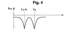
キャパシタ8のない共振周波数の位置を、図3に示す。S11は、給電点で測定された反射ファクタである。共振周波数f1とf2では、これらの周波数では、アンテナが給電高周波数パワーの大部分を放出するので、反射ファクタは他の周波数よりかなり小さい。周波数f2は、周波数f1の値の3倍である。図4は、キャパシタ8が存在するときの状態を示す。周波数f’1は、f1と比較して極くわずかに低減されており、したがって、ほぼ値f1を有するが、より高い共振周波数f’2は、図3のf2と比較して、かなり低減されている。
【0039】
当業者なら、他の影響(手持ち式無線通信装置、特にGSM携帯電話の収容、装置を持っている手の影響および他の影響)が、理論的な考察、またインストールしていない状態で動作したアンテナ構成に基づいて、長さに認識できる変化を引き起こすことがあり得ることに気付くであろう。したがって、ここで説明した構成に対する寸法決めの規則と比較して、繊細な調整も場合によっては必要となる可能性がある。
【0040】
平面図では、図1による構成で提供されている5つのラジエータセクション3bから3fは、小文字「e」の概形を形成する。したがって、eパッチという名称が、この構成に対して提案されている。
【0041】
アンテナ構成1は、制限されている利用可能な空間を、高周波数伝導ラジエータ表面区域で満たすように設計されている。セクション3eに隣接するセクション3fも、この目的のために役立つ。セクション3fは、直線的なラジエータの長さ1(各セクションのそれぞれの中央線に沿って測定した長さよりいくらか短い)の一部分を形成し、セクション3cの付近にあるために、キャパシタ8に実用的な接続の選択肢を提供する。より低い共振周波数では、ラジエータ3はё/4ラジエータであり、ラジエータ3は、その全長に沿って放出する。しかし、これはまた、より高い共振周波数での場合でもある。ここで再び、ラジエータ3は、長さがより短いセクションだけでなく、全てのセクション3aから3fで放出する。これは、アンテナ構成が、より高い共振周波数でも比較的広い帯域を有するので、重要な利点である。反対に、上述したように、アンテナは、一方ではGSM1800の受信範囲に、他方ではGSM1800の送信範囲にアンテナ構成を最適に適応させるために、切替え適応機能を要求する可能性がある。アンテナがGSM1800でなくGSM1900用の寸法であるとき、またはAMPSなど他の規格を使用するとき、これらの実施形態も直接使用するべきであることが明らかになるであろう。
【0042】
特に、図1による例示的な実施形態の場合では、ラジエータ3の表面区域の本質的な部分が、キャパシタ8の接続のために失われていないことに留意されたい。キャパシタ8は、単純に、ゾーン6と7の間で接続することができる。
【0043】
アンテナ構成1’の好ましい実施形態(図5)は、キャパシタ8がシート金属片20によって形成され、幅がセクション3fの幅にほぼ対応し、自由端6とセクション3cの間のギャップ上に配置され、、2つの隣接するセクション3cと3fには十分に重なり、誘電材料の挿入された層(合成樹脂シート22、図5a参照)で、これらの部分にそれから定義された距離のところで接続される。このようにして2つのキャパシタが形成され、比較的広くて短く、したがって低誘導性である接続線を介して互いに直列に接続される。
【0044】
アンテナの最適な寸法決めのために、特にキャパシタ8の容量値と接続点7は可変である。例えば、図2による値dが、長さ1/3よりいくらか長いセクション3cの点でキャパシタを接続することが有用である可能性があるが、これは、接地プレートからの距離をそのように増大しても、より高い共振周波数でキャパシタを横切って生じる電圧には小さな変化しか起きないが(点d=1/3は、曲線11の最大値のところで生じるからである)、対応する曲線10の電圧(より低い周波数範囲)では、より大きな変化が生じ、したがって、このようにして、より低い共振周波数に対するキャパシタの影響を、さらにいくらか低減することができるからである。
【0045】
簡単な図面、図5は、部分的に割愛した手持ち式無線通信装置15、すなわち移動電話を示し、アンテナとして上述したアンテナ構成1’を含む、。このアンテナの場合、キャパシタは、シート金属片20によって形成され、挿入された絶縁層と共に3cと3fの部分上に配置され、2つのキャパシタンスとして直列接続されている。短絡プレート3aは、移動電話のハウジングの上端に向かって配置されている。例では、手持ち式無線通信装置は、GSM900とGSM1800の範囲用に設計されている。アンテナ構成は、移動電話の内部に完全に収容されており、したがって、統合されたアンテナを形成している。
【0046】
GSM900とGSM1800の範囲の移動電話に対する図1によるアンテナ構成の特別な例示的実施形態では、ラジエータは、約5cm×4cm×0.5cm(後者は短絡プレートの長さである)の空間を占有する。
【0047】
図1から明らかなように、キャパシタの接続点7およびゾーン6と点7が非常に近接していることのために、ラジエータの長さと1/3から2/3の長さの再分割を維持しながら、本発明の原理から逸脱せずに、ラジエータのセクションの形状を著しく変更することが可能である。
【0048】
説明したように、キャパシタ8への短い給電線により、必要な空間は小さく、損失は比較的少ない。小さな空間要件により、最大限可能な帯域幅に対する寸法決めが可能になる。
【0049】
また、アンテナ構成の給電が、両方の周波数の帯域に対して同じ接続点で、すなわちラジエータ3への給電線5の接続点で、行われることを強調すべきである。
【0050】
図1による構成で、より高い共振周波数が、キャパシタ8を省略し、ラジエータ3の自由端と接地との間でキャパシタを接続することによって低減される場合、これはまた、より低い共振周波数をかなり低減することになり、より高い共振周波数とより低い共振周波数の周波数の割合3:1にはほとんど変化が生じず、したがって、このタイプの回路は使用できないことになる。
【図面の簡単な説明】
【図1】アンテナの例示的な実施形態の概略的な透視図である。
【図2】キャパシタを含まない、図1によるアンテナの長さに沿った、2つの共振周波数の電圧分布のグラフの図である。
【図3】図1によるキャパシタが存在しない、図1によるアンテナの2共振周波数の位置を示す図である。
【図4】図1によるキャパシタが存在する結果として、図3と比較して共振周波数の変更した位置を、図3と同じ周波数のスケールで示す図である。
【図5】アンテナを有する手持ち式移動電話装置の図である。
【図5a】拡張したスケールで、図5の20の詳細を示す図である。
【符号の説明】
1、1’ アンテナ構成
2 接地プレート
3 ラジエータ
3a 短絡プレート
3b、3c、3d、3e、3f ラジエータ3のセクション
5 給電線
6 ゾーン
7 キャパシタ8の接続点
8 キャパシタ
9 同軸ケーブル
10 電圧特性曲線
11 電界特性曲線
15 手持ち式無線通信装置
20 シート金属片
22 合成樹脂シート
f1、f2、f’1、f’2 共振周波数
S11 反射ファクタ[0001]
BACKGROUND OF THE INVENTION
The present invention comprises an antenna arrangement comprising a ground plate and a radiator disposed at a distance from the ground plate, substantially parallel to the ground plate and electrically conductively connected to the ground plate in one of its end zones. Flat antenna configuration, plate antenna configuration, patch antenna configuration). At the first resonance frequency of the antenna configuration, a minimum voltage is generated at the connection point between the radiator and the ground plate, and a first maximum voltage is generated in the region of the other end (free end) of the radiator.
[0002]
[Prior art]
Integrated antennas for mobile phones based on the principle of patch antennas are known. In existing applications, the outer dimensions of such antenna modules are minimized, for example, by using a folding structure (such as a C patch). In addition to a single resonant design (single operating frequency band), there are other structures that facilitate operation in two defined frequency bands (eg, in the two mobile radio communication bands of the GSM900 and GSM1800 standards). Are known. Here, two separate radiators are used, or only a specific part of the radiator is used at a higher operating frequency, using appropriate means. These procedures have the disadvantage that they do not utilize the entire available antenna volume, especially at higher frequencies. As a result, the antenna has a narrow bandwidth.
[0003]
[Problems to be solved by the invention]
The object of the present invention is to provide a configuration of the type described in the introduction, which is suitable for two frequency ranges and allows the construction of a wide band.
[0004]
[Means for Solving the Problems]
This object is achieved in accordance with the
[0005]
An advantage of the present invention is that the entire radiator emits radiation in both frequency ranges. In this way, since a large radiator surface area is available, a relatively wide bandwidth is possible even at higher frequencies. There is also an advantage at lower frequencies, even at low frequencies, since the entire surface area available for the antenna can be used as a radiator. One single point of the radiator can be used for feeding.
[0006]
In an embodiment of the present invention, the connection point between the capacitance value and the capacitive coupling is selected such that the second resonant frequency is at least approximately approximate to twice the first resonant frequency. It is an advantage that it is suitable for operation in the 900/1800 MHz or 900/1900 MHz band.
[0007]
In an embodiment of the present invention, the capacitance value and other points are selected such that the first resonance frequency is reduced below the second resonance frequency. It is an advantage that the dimensions of the antenna can be kept small.
[0008]
In the embodiment of the present invention, the other point of the radiator described above is capacitively coupled at that point, and is arranged near the first maximum voltage on the radiator at the second resonance frequency. It is an advantage that the second resonance frequency is particularly greatly reduced and the reduction of the first resonance frequency is small.
[0009]
In embodiments of the present invention, the other points described above are located at about one third of the linear length of the radiator as measured from the connection to the ground plate. This dimension is preferred in many cases.
[0010]
In embodiments of the present invention, the radiator has a shape that is at least partially similar to C, including a non-circular, angular configuration that is generally C-shaped. This has proven favorable.
[0011]
In an embodiment of the invention, the shape of the radiator is selected such that the free end of the radiator is adjacent to the point of the radiator corresponding to the desired other capacitance connection point. Capacitor short connection lines are thereby advantageous.
[0012]
In embodiments of the present invention, capacitive coupling is a layer of inserted dielectric material that includes a portion of the length of the free end zone and a portion of the radiator at another point provided for capacitive coupling. It is formed by a covering metal piece, and thus capacitive coupling is formed by a series connection of two capacitors. A simple and space-saving configuration is an advantage.
[0013]
The present invention also relates to a handheld wireless communication device having an antenna including a transceiver for at least one of the purposes of voice transmission, data transmission, and video transmission. The antenna is substantially formed by an antenna configuration according to one of the above-mentioned claims. The advantage is that a simple transmission / reception circuit is possible. It is also possible for the device to have a small structural shape.
[0014]
The present invention also relates to the use of the antenna configuration described above and the design of a handheld wireless communication device. According to the invention, only the second (higher) resonant frequency of the antenna configuration is used in operation. This can have the potential advantage when only higher frequency bands are required, but according to the present invention, a two-band antenna can be used.
[0015]
Other features and advantages of the invention are set forth in the exemplary embodiments of the invention described below and in the claims with reference to the drawings showing essential details of the invention. Individual features may be implemented individually or in any combination in the embodiments of the present invention.
[0016]
DETAILED DESCRIPTION OF THE INVENTION
In FIG. 1, the
[0017]
In the embodiment of the present invention, the
[0018]
In the case of transmission and reception, the power supply of the
[0019]
At a height h corresponding to the length of the short-
[0020]
The above-described low-ohm feed of the feed line 5 is represented in FIG. 1 by a coaxial cable 9 extending from the bottom toward the
[0021]
In practical applications, the coaxial cable 9 is often much shorter than shown, or in an embodiment of the invention, the electronic circuit connected to the
[0022]
In the description of the functional mode of the antenna configuration shown in FIG. 1, reference is first made to FIG. 2, which is based on the antenna according to FIG. The distance d of the connection point or these short plate and the ground plate is plotted on the horizontal axis to the free end of the
[0023]
A
[0024]
When the feeder line 5 is fed at this first resonance frequency, the voltage has a first maximum value at the free end of the radiator, corresponding to a
[0025]
The next highest resonance frequency becomes effective when the feed frequency increases and the maximum value occurs again at the
[0026]
This type of configuration (without a capacitor) is an antenna configuration that operates in two frequency ranges that operate with electromagnetic waves and have significantly different frequencies (not factor 3), for example, frequencies that differ by approximately
[0027]
However, the embodiment shown in FIG. 1 facilitates such dual band operation.
[0028]
In fact, the antenna configuration described above has a narrow band and is tuned for transmission and reception even in the case of a mobile phone operating exclusively according to the GSM 900 standard and even when the transmission and reception operations are performed in a band separated by a certain frequency gap. Must be performed by each connecting means provided at the feeding point. The present invention is not related to this problem, and this problem is not necessarily solved by the present invention.
[0029]
Rather, according to the present invention, there is no need to bother switching between two frequency bands (eg, between 900 MHz and 1800 MHz as described) in the antenna region. Only one feeder 5 is used for electricity.
[0030]
In the configuration according to FIG. 1, this configuration is here where the connection point 7 of the capacitor 8 is arranged at approximately one third of the linear overall length of the
[0031]
Conversely, when
[0032]
It can be easily seen from FIG. 2 that the capacitor 8 is connected to a voltage that is twice the voltage at the free end of the
[0033]
Also, the lower resonant frequency is somewhat affected in terms of antenna length (frequency reduction), so
[0034]
As already mentioned, the higher resonant frequency is reduced to a considerable extent, and thus this higher frequency has the value required for GSM 1800 when the size of capacitor 8 is properly selected.
[0035]
According to the general theory relating to the connection point of the capacitor 8, the capacitor is connected to the radiator, thereby affecting (ie reducing) the higher resonance frequency more than the lower resonance frequency. More specifically, in this theory, at the connection point of the capacitor, the resulting voltage is greater at a higher resonance frequency than at a lower resonance frequency. In a specific example, the capacitor 8 is connected in the vicinity of the position where the maximum value of the voltage curve where the two phases of the second resonance frequency are opposite occurs.
[0036]
Note that there is currently another GSM standard (GSM 1900) that operates at even higher frequencies of about 1900 MHz. This frequency is also quite different from the first resonance frequency, in particular about twice, and can therefore be implemented in the same way according to the invention.
[0037]
The frequency ranges are about 880 to 960 MHz for GSM900, about 1710 to 1880 MHz for GSM1800, and about 1850 to 1990 MHz for GSM1900.
[0038]
The position of the resonance frequency without the capacitor 8 is shown in FIG. S 11 is the reflection factor measured at the feed point. At resonance frequencies f1 and f2, at these frequencies, the antenna emits most of the fed high frequency power, so the reflection factor is much smaller than the other frequencies. The frequency f2 is three times the value of the frequency f1. FIG. 4 shows the state when the capacitor 8 is present. The frequency f′1 is only slightly reduced compared to f1, and thus has approximately the value f1, but the higher resonant frequency f′2 is considerably reduced compared to f2 in FIG. ing.
[0039]
The person skilled in the art worked with other influences (containment of handheld wireless communication devices, especially GSM mobile phones, hand holding equipment and other influences) theoretical considerations and even without installation It will be noted that based on the antenna configuration, a perceptible change in length can be caused. Therefore, in some cases, delicate adjustments may be required as compared to the sizing rules for the configuration described herein.
[0040]
In the plan view, the five
[0041]
[0042]
In particular, it should be noted that in the case of the exemplary embodiment according to FIG. 1, an essential part of the surface area of the
[0043]
In a preferred embodiment of the
[0044]
In particular, the capacitance value of the capacitor 8 and the connection point 7 are variable for optimal sizing of the antenna. For example, it may be useful to connect a capacitor at the point of
[0045]
A simple drawing, FIG. 5, shows a partially omitted handheld
[0046]
In the particular exemplary embodiment of the antenna configuration according to FIG. 1 for mobile phones in the range of GSM 900 and GSM 1800, the radiator occupies a space of about 5 cm × 4 cm × 0.5 cm (the latter being the length of the shorting plate) .
[0047]
As can be seen from FIG. 1, the capacitor junction 7 and the
[0048]
As explained, the short feed line to the capacitor 8 requires a small space and relatively little loss. Small space requirements allow for sizing for the maximum possible bandwidth.
[0049]
It should also be emphasized that the feeding of the antenna configuration takes place at the same connection point for both frequency bands, ie at the connection point of the feed line 5 to the
[0050]
In the configuration according to FIG. 1, if the higher resonant frequency is reduced by omitting the capacitor 8 and connecting a capacitor between the free end of the
[Brief description of the drawings]
FIG. 1 is a schematic perspective view of an exemplary embodiment of an antenna.
2 is a graph of the voltage distribution of two resonant frequencies along the length of the antenna according to FIG. 1 without capacitors.
3 shows the position of the two resonance frequencies of the antenna according to FIG. 1 without the capacitor according to FIG. 1;
4 is a diagram showing the position where the resonance frequency is changed compared to FIG. 3 as a result of the presence of the capacitor according to FIG. 1 on a scale of the same frequency as in FIG. 3;
FIG. 5 is a diagram of a handheld mobile telephone device having an antenna.
FIG. 5a shows details of 20 of FIG. 5 on an expanded scale.
[Explanation of symbols]
1, 1 '
Claims (10)
Applications Claiming Priority (2)
| Application Number | Priority Date | Filing Date | Title |
|---|---|---|---|
| DE10022107.6 | 2000-05-08 | ||
| DE10022107A DE10022107A1 (en) | 2000-05-08 | 2000-05-08 | Integrated antenna for mobile phones |
Publications (3)
| Publication Number | Publication Date |
|---|---|
| JP2002009539A JP2002009539A (en) | 2002-01-11 |
| JP2002009539A5 JP2002009539A5 (en) | 2008-06-19 |
| JP4823433B2 true JP4823433B2 (en) | 2011-11-24 |
Family
ID=7641017
Family Applications (1)
| Application Number | Title | Priority Date | Filing Date |
|---|---|---|---|
| JP2001129152A Expired - Fee Related JP4823433B2 (en) | 2000-05-08 | 2001-04-26 | Integrated antenna for mobile phone |
Country Status (7)
| Country | Link |
|---|---|
| US (1) | US6473044B2 (en) |
| EP (1) | EP1154518B1 (en) |
| JP (1) | JP4823433B2 (en) |
| AT (1) | ATE320088T1 (en) |
| AU (1) | AU4205101A (en) |
| DE (2) | DE10022107A1 (en) |
| HU (1) | HUP0101658A3 (en) |
Families Citing this family (21)
| Publication number | Priority date | Publication date | Assignee | Title |
|---|---|---|---|---|
| GB2366453A (en) * | 2000-08-31 | 2002-03-06 | Nokia Mobile Phones Ltd | An antenna device for a communication terminal |
| TW490885B (en) * | 2001-05-25 | 2002-06-11 | Chi Mei Comm Systems Inc | Broadband dual-band antenna |
| TW529779U (en) * | 2001-10-26 | 2003-04-21 | Hon Hai Prec Ind Co Ltd | Multi-frequency antenna |
| US6577277B1 (en) * | 2001-12-21 | 2003-06-10 | Hon Hai Precision Ind. Co., Ltd. | Dual band antenna |
| JP2004128605A (en) * | 2002-09-30 | 2004-04-22 | Murata Mfg Co Ltd | Antenna structure and communication system therewith |
| US6903686B2 (en) | 2002-12-17 | 2005-06-07 | Sony Ericsson Mobile Communications Ab | Multi-branch planar antennas having multiple resonant frequency bands and wireless terminals incorporating the same |
| US6980154B2 (en) | 2003-10-23 | 2005-12-27 | Sony Ericsson Mobile Communications Ab | Planar inverted F antennas including current nulls between feed and ground couplings and related communications devices |
| KR100693416B1 (en) * | 2004-09-24 | 2007-03-12 | 엘지전자 주식회사 | Character pattern Antenna |
| JP4529786B2 (en) * | 2005-04-28 | 2010-08-25 | 株式会社日立製作所 | Signal processing circuit and non-contact IC card and tag using the same |
| DE102005038196A1 (en) * | 2005-08-12 | 2007-02-22 | Hirschmann Car Communication Gmbh | Low-profile mobile radio antenna for a vehicle |
| DE102005049820A1 (en) * | 2005-10-18 | 2007-04-19 | Benq Mobile Gmbh & Co. Ohg | Multi-resonant antenna unit, associated printed circuit board and radio communication device |
| KR101027293B1 (en) | 2006-12-22 | 2011-04-06 | 가부시키가이샤 무라타 세이사쿠쇼 | Antenna structure and wireless communication apparatus with that antenna structure |
| JP4858860B2 (en) * | 2007-10-10 | 2012-01-18 | 日立金属株式会社 | Multiband antenna |
| JP4968226B2 (en) | 2008-09-30 | 2012-07-04 | 富士通株式会社 | Antenna and reader / writer device |
| JP5133186B2 (en) * | 2008-09-30 | 2013-01-30 | 株式会社フジクラ | antenna |
| US20110206097A1 (en) * | 2010-02-19 | 2011-08-25 | Sony Ericsson Mobile Communications Ab | Terminals and antenna systems with a primary radiator line capacitively excited by a secondary radiator line |
| US8456366B2 (en) | 2010-04-26 | 2013-06-04 | Sony Corporation | Communications structures including antennas with separate antenna branches coupled to feed and ground conductors |
| US8108021B2 (en) | 2010-05-27 | 2012-01-31 | Sony Ericsson Mobile Communications Ab | Communications structures including antennas with filters between antenna elements and ground sheets |
| CN102683837B (en) * | 2012-05-14 | 2014-04-16 | 天津大学 | Dual-frequency microstrip patch antenna based on combined left/right hand transmission wire |
| FR3026895B1 (en) * | 2014-10-06 | 2017-12-08 | Renault Sas | FLAT ANTENNA WITH RADIANT ELEMENT IN SPIRAL |
| WO2017064947A1 (en) * | 2015-10-14 | 2017-04-20 | 株式会社村田製作所 | Antenna device |
Family Cites Families (12)
| Publication number | Priority date | Publication date | Assignee | Title |
|---|---|---|---|---|
| FR2699740B1 (en) * | 1992-12-23 | 1995-03-03 | Patrice Brachat | Broadband antenna with reduced overall dimensions, and corresponding transmitting and / or receiving device. |
| JPH0955608A (en) * | 1995-08-11 | 1997-02-25 | Fujitsu Ltd | Directivity coupler |
| EP0777295B1 (en) * | 1995-11-29 | 2003-05-28 | Ntt Mobile Communications Network Inc. | Antenna device having two resonance frequencies |
| JPH09232856A (en) * | 1996-02-22 | 1997-09-05 | Matsushita Electric Ind Co Ltd | Planar antenna |
| JP2898921B2 (en) * | 1996-06-20 | 1999-06-02 | 株式会社ヨコオ | Antennas and radios |
| DE19707535A1 (en) * | 1997-02-25 | 1998-08-27 | Rothe Lutz Dr Ing Habil | Foil emitter |
| EP0884796A3 (en) * | 1997-06-11 | 1999-03-24 | Matsushita Electric Industrial Co., Ltd. | Antenna device consisting of bent or curved portions of linear conductor |
| JP3438016B2 (en) * | 1998-03-03 | 2003-08-18 | 株式会社ケンウッド | Multi-frequency resonant inverted-F antenna |
| EP1011167A4 (en) * | 1998-07-02 | 2005-10-12 | Matsushita Electric Ind Co Ltd | Antenna unit, communication system and digital television receiver |
| US6353443B1 (en) * | 1998-07-09 | 2002-03-05 | Telefonaktiebolaget Lm Ericsson (Publ) | Miniature printed spiral antenna for mobile terminals |
| US6166694A (en) * | 1998-07-09 | 2000-12-26 | Telefonaktiebolaget Lm Ericsson (Publ) | Printed twin spiral dual band antenna |
| JP2001189615A (en) * | 1999-10-18 | 2001-07-10 | Matsushita Electric Ind Co Ltd | Antenna for mobile radio and portable radio equipment using the same |
-
2000
- 2000-05-08 DE DE10022107A patent/DE10022107A1/en active Pending
-
2001
- 2001-04-25 HU HU0101658A patent/HUP0101658A3/en unknown
- 2001-04-26 JP JP2001129152A patent/JP4823433B2/en not_active Expired - Fee Related
- 2001-05-03 AU AU42051/01A patent/AU4205101A/en not_active Abandoned
- 2001-05-04 AT AT01440125T patent/ATE320088T1/en not_active IP Right Cessation
- 2001-05-04 DE DE50109152T patent/DE50109152D1/en not_active Expired - Lifetime
- 2001-05-04 EP EP01440125A patent/EP1154518B1/en not_active Expired - Lifetime
- 2001-05-07 US US09/849,355 patent/US6473044B2/en not_active Expired - Lifetime
Also Published As
| Publication number | Publication date |
|---|---|
| EP1154518A2 (en) | 2001-11-14 |
| EP1154518A3 (en) | 2002-08-28 |
| HU0101658D0 (en) | 2001-06-28 |
| US20020005809A1 (en) | 2002-01-17 |
| ATE320088T1 (en) | 2006-03-15 |
| DE10022107A1 (en) | 2001-11-15 |
| HUP0101658A2 (en) | 2002-01-28 |
| JP2002009539A (en) | 2002-01-11 |
| DE50109152D1 (en) | 2006-05-04 |
| US6473044B2 (en) | 2002-10-29 |
| EP1154518B1 (en) | 2006-03-08 |
| HUP0101658A3 (en) | 2002-09-30 |
| AU4205101A (en) | 2001-11-15 |
Similar Documents
| Publication | Publication Date | Title |
|---|---|---|
| JP4823433B2 (en) | Integrated antenna for mobile phone | |
| US5764190A (en) | Capacitively loaded PIFA | |
| JP4089680B2 (en) | Antenna device | |
| US6542126B2 (en) | Antenna arrangement for mobile radiotelephones | |
| US8212731B2 (en) | Antenna device and communication apparatus | |
| KR100799875B1 (en) | Chip antenna and mobile-communication terminal comprising the same | |
| EP1569300B1 (en) | Wireless device having antenna | |
| US6700543B2 (en) | Antenna element with conductors formed on outer surfaces of device substrate | |
| KR101150683B1 (en) | An antenna arrangement | |
| KR100707242B1 (en) | Dielectric chip antenna | |
| US6839040B2 (en) | Antenna for a communication terminal | |
| JP2005510927A (en) | Dual band antenna device | |
| JP2007013981A (en) | Internal chip antenna | |
| US20020177416A1 (en) | Radio communications device | |
| US7542002B1 (en) | Wideband monopole antenna | |
| US6795027B2 (en) | Antenna arrangement | |
| WO2015011468A1 (en) | Multi-band antennas using loops or notches | |
| KR20020015694A (en) | Flat-plate monopole antennae | |
| JP6825429B2 (en) | Multi-band antenna and wireless communication device | |
| JPH09232854A (en) | Small planar antenna system for mobile radio equipment | |
| WO2001020714A1 (en) | Broadband or multi-band planar antenna | |
| KR100861865B1 (en) | Wireless terminal | |
| JP4329579B2 (en) | Antenna device | |
| EP1253667A1 (en) | Patch antenna | |
| KR100862492B1 (en) | Chip antenna and mobile-communication terminal comprising the same |
Legal Events
| Date | Code | Title | Description |
|---|---|---|---|
| A521 | Request for written amendment filed |
Free format text: JAPANESE INTERMEDIATE CODE: A523 Effective date: 20080425 |
|
| A621 | Written request for application examination |
Free format text: JAPANESE INTERMEDIATE CODE: A621 Effective date: 20080425 |
|
| A977 | Report on retrieval |
Free format text: JAPANESE INTERMEDIATE CODE: A971007 Effective date: 20100603 |
|
| A131 | Notification of reasons for refusal |
Free format text: JAPANESE INTERMEDIATE CODE: A131 Effective date: 20100608 |
|
| A601 | Written request for extension of time |
Free format text: JAPANESE INTERMEDIATE CODE: A601 Effective date: 20100902 |
|
| A602 | Written permission of extension of time |
Free format text: JAPANESE INTERMEDIATE CODE: A602 Effective date: 20100907 |
|
| A521 | Request for written amendment filed |
Free format text: JAPANESE INTERMEDIATE CODE: A523 Effective date: 20101207 |
|
| A131 | Notification of reasons for refusal |
Free format text: JAPANESE INTERMEDIATE CODE: A131 Effective date: 20110426 |
|
| A521 | Request for written amendment filed |
Free format text: JAPANESE INTERMEDIATE CODE: A523 Effective date: 20110725 |
|
| TRDD | Decision of grant or rejection written | ||
| A01 | Written decision to grant a patent or to grant a registration (utility model) |
Free format text: JAPANESE INTERMEDIATE CODE: A01 Effective date: 20110830 |
|
| A01 | Written decision to grant a patent or to grant a registration (utility model) |
Free format text: JAPANESE INTERMEDIATE CODE: A01 |
|
| A61 | First payment of annual fees (during grant procedure) |
Free format text: JAPANESE INTERMEDIATE CODE: A61 Effective date: 20110907 |
|
| R150 | Certificate of patent or registration of utility model |
Ref document number: 4823433 Country of ref document: JP Free format text: JAPANESE INTERMEDIATE CODE: R150 Free format text: JAPANESE INTERMEDIATE CODE: R150 |
|
| FPAY | Renewal fee payment (event date is renewal date of database) |
Free format text: PAYMENT UNTIL: 20140916 Year of fee payment: 3 |
|
| R250 | Receipt of annual fees |
Free format text: JAPANESE INTERMEDIATE CODE: R250 |
|
| R250 | Receipt of annual fees |
Free format text: JAPANESE INTERMEDIATE CODE: R250 |
|
| R250 | Receipt of annual fees |
Free format text: JAPANESE INTERMEDIATE CODE: R250 |
|
| R250 | Receipt of annual fees |
Free format text: JAPANESE INTERMEDIATE CODE: R250 |
|
| R250 | Receipt of annual fees |
Free format text: JAPANESE INTERMEDIATE CODE: R250 |
|
| LAPS | Cancellation because of no payment of annual fees |