EP1569300B1 - Wireless device having antenna - Google Patents
Wireless device having antenna Download PDFInfo
- Publication number
- EP1569300B1 EP1569300B1 EP05000402A EP05000402A EP1569300B1 EP 1569300 B1 EP1569300 B1 EP 1569300B1 EP 05000402 A EP05000402 A EP 05000402A EP 05000402 A EP05000402 A EP 05000402A EP 1569300 B1 EP1569300 B1 EP 1569300B1
- Authority
- EP
- European Patent Office
- Prior art keywords
- antenna element
- wireless device
- coupled
- antenna
- feeding point
- Prior art date
- Legal status (The legal status is an assumption and is not a legal conclusion. Google has not performed a legal analysis and makes no representation as to the accuracy of the status listed.)
- Expired - Fee Related
Links
- 230000005540 biological transmission Effects 0.000 claims description 12
- 239000011347 resin Substances 0.000 claims description 7
- 229920005989 resin Polymers 0.000 claims description 7
- 239000003990 capacitor Substances 0.000 claims description 6
- 239000002184 metal Substances 0.000 claims description 5
- 230000003071 parasitic effect Effects 0.000 claims description 3
- 238000003825 pressing Methods 0.000 claims description 3
- 238000005476 soldering Methods 0.000 claims description 3
- 238000010276 construction Methods 0.000 description 10
- 230000008878 coupling Effects 0.000 description 5
- 238000010168 coupling process Methods 0.000 description 5
- 238000005859 coupling reaction Methods 0.000 description 5
- 230000005855 radiation Effects 0.000 description 5
- ORQBXQOJMQIAOY-UHFFFAOYSA-N nobelium Chemical compound [No] ORQBXQOJMQIAOY-UHFFFAOYSA-N 0.000 description 4
- 238000004891 communication Methods 0.000 description 3
- 238000010295 mobile communication Methods 0.000 description 3
- 230000001413 cellular effect Effects 0.000 description 2
- 230000005611 electricity Effects 0.000 description 2
- 239000000758 substrate Substances 0.000 description 2
- 229910000906 Bronze Inorganic materials 0.000 description 1
- OAICVXFJPJFONN-UHFFFAOYSA-N Phosphorus Chemical compound [P] OAICVXFJPJFONN-UHFFFAOYSA-N 0.000 description 1
- 239000010974 bronze Substances 0.000 description 1
- 150000001875 compounds Chemical class 0.000 description 1
- KUNSUQLRTQLHQQ-UHFFFAOYSA-N copper tin Chemical compound [Cu].[Sn] KUNSUQLRTQLHQQ-UHFFFAOYSA-N 0.000 description 1
- 230000001419 dependent effect Effects 0.000 description 1
- 239000003989 dielectric material Substances 0.000 description 1
- 230000009977 dual effect Effects 0.000 description 1
- 230000005404 monopole Effects 0.000 description 1
Images
Classifications
-
- H—ELECTRICITY
- H01—ELECTRIC ELEMENTS
- H01Q—ANTENNAS, i.e. RADIO AERIALS
- H01Q21/00—Antenna arrays or systems
- H01Q21/30—Combinations of separate antenna units operating in different wavebands and connected to a common feeder system
-
- H—ELECTRICITY
- H01—ELECTRIC ELEMENTS
- H01Q—ANTENNAS, i.e. RADIO AERIALS
- H01Q1/00—Details of, or arrangements associated with, antennas
- H01Q1/12—Supports; Mounting means
- H01Q1/22—Supports; Mounting means by structural association with other equipment or articles
- H01Q1/24—Supports; Mounting means by structural association with other equipment or articles with receiving set
- H01Q1/241—Supports; Mounting means by structural association with other equipment or articles with receiving set used in mobile communications, e.g. GSM
- H01Q1/242—Supports; Mounting means by structural association with other equipment or articles with receiving set used in mobile communications, e.g. GSM specially adapted for hand-held use
- H01Q1/243—Supports; Mounting means by structural association with other equipment or articles with receiving set used in mobile communications, e.g. GSM specially adapted for hand-held use with built-in antennas
-
- H—ELECTRICITY
- H01—ELECTRIC ELEMENTS
- H01Q—ANTENNAS, i.e. RADIO AERIALS
- H01Q1/00—Details of, or arrangements associated with, antennas
- H01Q1/36—Structural form of radiating elements, e.g. cone, spiral, umbrella; Particular materials used therewith
- H01Q1/38—Structural form of radiating elements, e.g. cone, spiral, umbrella; Particular materials used therewith formed by a conductive layer on an insulating support
-
- H—ELECTRICITY
- H01—ELECTRIC ELEMENTS
- H01Q—ANTENNAS, i.e. RADIO AERIALS
- H01Q5/00—Arrangements for simultaneous operation of antennas on two or more different wavebands, e.g. dual-band or multi-band arrangements
- H01Q5/40—Imbricated or interleaved structures; Combined or electromagnetically coupled arrangements, e.g. comprising two or more non-connected fed radiating elements
-
- H—ELECTRICITY
- H01—ELECTRIC ELEMENTS
- H01Q—ANTENNAS, i.e. RADIO AERIALS
- H01Q9/00—Electrically-short antennas having dimensions not more than twice the operating wavelength and consisting of conductive active radiating elements
- H01Q9/04—Resonant antennas
- H01Q9/30—Resonant antennas with feed to end of elongated active element, e.g. unipole
- H01Q9/42—Resonant antennas with feed to end of elongated active element, e.g. unipole with folded element, the folded parts being spaced apart a small fraction of the operating wavelength
Definitions
- the present invention relates to a wireless device having an antenna, and more particularly it relates to a wireless device such as a cellular phone to be used in a mobile communication.
- the mobile communication including cellular phones provides versatile services in data communication such as communications in audio, text and dynamic picture.
- This market trend requires a more sophisticated wireless device, in particular, a wireless device having a more sophisticated antenna is demanded.
- the antenna is a gate for receiving and transmitting an electromagnetic wave, and its performance is one of large factors affecting the performance of the wireless device.
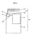
- FIG. 3 illustrates schematically the conventional wireless device having an antenna.
- antenna 103 is placed side by side with ground plane 108.
- Antenna 103 includes antenna element 101 for resonating with a first frequency and antenna element 102 for resonating with a second frequency.
- Antenna 103 is coupled to feeding point 104 disposed on ground plane 108, and coupled to radio circuit 107 via matching circuit 105 and transmission circuit 106.
- the structure discussed above forms wireless device 109.
- First antenna element 101 resonates with the frequency ranging from 880 MHz - 960 MHz, namely, GSM (Global System of Mobile Communication) band
- second antenna element 102 resonates with the frequency ranging from 1710 MHz - 1880 MHz, namely, DCS (Digital Communication System) band.
- first antenna element 101 When the wireless device discussed above receives a frequency of GSM band, first antenna element 101 energizes an electric current using an electromagnetic wave received, and the current runs to radio circuit 107 via feeding point 104, matching circuit 105 and transmission line 106. As a result, the electromagnetic wave is received by the wireless device.
- a signal generated in radio circuit 107 is conveyed to first antenna element 101 via transmission line 106, matching circuit 105 and feeding point 104.
- First antenna element 101 energizes the signal into an electromagnetic wave, which is then radiated, thereby carrying out a transmission.
- second antenna element 102 When the wireless device receives/transmits a frequency of DCS band, second antenna element 102 receives/transmits an electromagnetic wave in the same manner as the case of receiving/transmitting an electromagnetic wave of GSM band.
- the construction of the conventional wireless device allows one single feeding point 104 to feed both of antenna elements 101 and 102 with electricity, the coupling between elements 101 and 102 is strengthened. Therefore, when an electromagnetic wave is radiated from one antenna, the power radiated travels to the other antenna, so that the one antenna tends to invite some loss in its radiating power.
- matching circuit 105 adjusts two different electromagnetic waves independently by itself in order to obtain two different and desirable resonant frequencies, so that when a first resonance frequency is adjusted, a second one changes synchronously. As a result, it is difficult to adjust only the first resonance frequency efficiently and independently of the second one.
- the antenna device has a feed element provided on the surface of a substrate.
- the feed element comprises two branched radiation electrodes.
- a strip-shaped non-feed radiation electrode is provided adjacent to each branched radiation electrode.
- the substrate is made of a dielectric material.
- the branched radiation electrodes are mutually different in length corresponding a frequency band of 800 to 900 MHz and a frequency band of 1800 to 1900 MHz, respectively.
- the branched radiation electrodes have a common feeding end. To this feeding end an electric signal is supplied from a signal source by way of an impedance matching circuit.
- the present invention aims to overcome the problems discussed above, and provides a wireless device that can reduce a coupling loss of two antenna elements and adjust a frequency independently of other frequencies to a desirable resonance frequency although the wireless device handles numbers of frequencies.
- a wireless device may comprise the following elements:
- the construction discussed above has two feeding points corresponding to the first antenna element and the second antenna element respectively and independently, so that a coupling loss between the two antenna elements can be reduced.
- the construction has two matching circuits corresponding to the two antenna elements respectively and independently, namely, the first matching circuit and the second one. It is easy to adjust two different resonant frequencies independently.
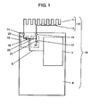
- Fig. 1 shows schematically a wireless device in accordance with the exemplary embodiment of the present invention.
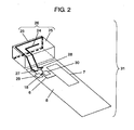
- Fig. 2 shows a perspective view illustrating a wireless device, having an antenna comprising antenna elements made of spring metal and insulating resin, in accordance with the exemplary embodiment of the present invention.
- Wireless device 19 comprises the following elements:
- antenna 13 is placed side by side with ground plane 8, and includes first antenna element 11 resonating with a first frequency and second antenna element 12 resonating with a second frequency.
- First antenna element 11 is coupled to first feeding point 14 placed on ground plane 8, and first feeding point 14 is coupled to a first end of first matching circuit 16.
- second antenna element 12 is coupled to second feeding point 15 placed on ground plane 8, and second feeding point 15 is coupled to a first end of second matching circuit 17.
- a second end of first matching circuit 16 and a second end of second matching circuit 17 are coupled to each other at common connection point 18, which is coupled to radio circuit 7 via transmission line 6.
- First antenna element 11 resonates with the first frequency, i.e. GSM band of 880 MHz - 960 MHz, and second antenna element 12 resonates the second frequency higher than the first one, i.e. DCS band of 17710 MHz - 1880 MHz.
- First matching circuit 16 is formed of inductor 20 coupled between first feeding point 14 and common connection point 18.
- Second matching circuit 17 is formed of capacitor 22 and inductor 21.
- Capacitor 22 is coupled between second feeding point 15 and common connection point 18, and inductor 21 is coupled between second feeding point 15 and ground plane 8.
- Wireless device 19 having the structure discussed above can receive or transmit the frequency of GSM band because first antenna element 11 resonates with the GSM frequency. It can also receive or transmit the frequency of DCS band because second antenna element 12 resonates with the DCS frequency.
- wireless device 19 has two feeding points corresponding to first antenna element 11 and second antenna element 12 respectively and independently, so that a coupling loss between the two antenna elements 11 and 12 can be reduced.
- wireless device 19 has two matching circuits 16 and 17 corresponding to two antenna elements 11 and 12 respectively and independently, thereby adjusting two different resonant frequencies independently with ease.
- matching circuits 16 and 17 produces the following advantages: When wireless device 19 handles the first frequency, second antenna element 12 is electrically isolated from transmission line 6 by capacitor 22 of second matching circuit 17. Further, second antenna element 12 is electrically coupled to ground plane 8 by inductor 21 of second matching circuit 17, so that second antenna element 12 works as a parasitic antenna element. As a result, the compound resonance between first antenna element 11 and second antenna element 12 working as a parasitic antenna element can widen a band of the first frequency.
- Inductor 20 of first matching circuit 16 works at the first frequency such that the resonance frequency of first antenna element 11 can be lowered, thereby downsizing first antenna element 11.
- Inductor 20 also works as a high impedance to the second frequency, so that it advantageously shuts off the electrical transmission of the second frequency to first antenna element 11. This mechanism allows adjusting the two frequencies independently more easily.
- the placement of the passive components such as capacitors and inductors of matching circuits 16 and 17 is not limited to what is shown in Fig. 1 , but the passive components can be placed arbitrarily so that the impedance can be adjusted. In this case, the foregoing idea is desirably adopted.
- First antenna element 11 shown in Fig. 1 is formed of a meander antenna; however, antenna element 11 is not limited to this construction, e.g. first antenna element 23 is formed of a folded monopole antenna as shown in Fig. 2 . It can be also any type of linear-, helical-, meander-, and planar-antenna or it can be constructed by combining those antenna types. Second antenna element 12 can be also any type of antenna as discussed above. A part of first antenna element 11 or a part of second antenna element 12 is grounded to ground plane 8, so that the antenna element can work as an inverted F antenna. This construction allows adjusting the impedance more flexibly.
- Fig. 2 shows a perspective view illustrating a wireless device, comprising an antenna formed of antenna elements made of spring metal and insulating resin, in accordance with the exemplary embodiment of the present invention.
- first antenna element 23 and second antenna element 24 are formed together with insulating resin 25, thereby forming antenna 26.
- insulating resin 25 suppresses deformation of first antenna element 23 and second antenna element 24, and antenna 26 can be downsized with ease thanks to the dielectric constant of insulating resin 25.
- first antenna element 23 and second antenna element 24 are made of spring metal such as phosphor bronze. An end of each antenna element is coupled to first feeding point 27 and second feeding point 28 respectively by applying pressure. This construction allows antenna 26 to be coupled to respective feeding points 27 and 28 with ease free from soldering.
- first end of first matching circuit 29 and a first end of second matching circuit 30 are coupled to first feeding point 27 and second feeding point 28 respectively. Second ends of each of circuits 29 and 30 are coupled to common connection point 18, which is coupled to radio circuit 7 via transmission line 6. Those structures remain unchanged from that shown in Fig. 1 .
- the foregoing construction allows wireless device 31 to adjust respective resonant frequencies corresponding to first antenna element 23 and second antenna element 24 independently with ease.
- the wireless device of the present invention has two feeding points corresponding to two antenna elements respectively and independently, so that a coupling loss between the two antenna elements can be reduced.
- the wireless device has two matching circuits corresponding to the two antenna elements respectively and independently, so that two independent resonant frequencies different from each other can be adjusted with ease. It is thus concluded that the present invention advantageously provides the foregoing wireless device having an antenna.
Landscapes
- Engineering & Computer Science (AREA)
- Computer Networks & Wireless Communication (AREA)
- Physics & Mathematics (AREA)
- Electromagnetism (AREA)
- Details Of Aerials (AREA)
- Support Of Aerials (AREA)
- Variable-Direction Aerials And Aerial Arrays (AREA)
- Waveguide Aerials (AREA)
- Transceivers (AREA)
Description
- The present invention relates to a wireless device having an antenna, and more particularly it relates to a wireless device such as a cellular phone to be used in a mobile communication.
- Recently the mobile communication including cellular phones provides versatile services in data communication such as communications in audio, text and dynamic picture. This market trend requires a more sophisticated wireless device, in particular, a wireless device having a more sophisticated antenna is demanded. Because the antenna is a gate for receiving and transmitting an electromagnetic wave, and its performance is one of large factors affecting the performance of the wireless device.
- A conventional wireless device is described hereinafter with reference to
Fig. 3 which illustrates schematically the conventional wireless device having an antenna. InFig. 3 ,antenna 103 is placed side by side withground plane 108.Antenna 103 includesantenna element 101 for resonating with a first frequency andantenna element 102 for resonating with a second frequency.Antenna 103 is coupled tofeeding point 104 disposed onground plane 108, and coupled toradio circuit 107 viamatching circuit 105 andtransmission circuit 106. The structure discussed above formswireless device 109. - As discussed above, the construction of conventional
wireless device 109 allows asingle feeding point 104 to feed both offirst antenna element 101 andsecond antenna element 102 with electricity.First antenna element 101 resonates with the frequency ranging from 880 MHz - 960 MHz, namely, GSM (Global System of Mobile Communication) band, andsecond antenna element 102 resonates with the frequency ranging from 1710 MHz - 1880 MHz, namely, DCS (Digital Communication System) band. - When the wireless device discussed above receives a frequency of GSM band,
first antenna element 101 energizes an electric current using an electromagnetic wave received, and the current runs toradio circuit 107 viafeeding point 104,matching circuit 105 andtransmission line 106. As a result, the electromagnetic wave is received by the wireless device. - When a frequency of GSM band is transmitted from the wireless device, a signal generated in
radio circuit 107 is conveyed tofirst antenna element 101 viatransmission line 106,matching circuit 105 andfeeding point 104.First antenna element 101 energizes the signal into an electromagnetic wave, which is then radiated, thereby carrying out a transmission. - When the wireless device receives/transmits a frequency of DCS band,
second antenna element 102 receives/transmits an electromagnetic wave in the same manner as the case of receiving/transmitting an electromagnetic wave of GSM band. - As such conventional
wireless device 109 deals with the two kinds of frequencies, i.e. GSM and DCS. Japanese patent application non-examined publication No.2003 - 101335 - However, since the construction of the conventional wireless device allows one
single feeding point 104 to feed both ofantenna elements elements - Further, matching
circuit 105 adjusts two different electromagnetic waves independently by itself in order to obtain two different and desirable resonant frequencies, so that when a first resonance frequency is adjusted, a second one changes synchronously. As a result, it is difficult to adjust only the first resonance frequency efficiently and independently of the second one. - Document
US 2002/0163470 A1 discloses an antenna device having plural frequency bands. The antenna device has a feed element provided on the surface of a substrate. The feed element comprises two branched radiation electrodes. In order to realize dual resonance in each frequency band, a strip-shaped non-feed radiation electrode is provided adjacent to each branched radiation electrode. The substrate is made of a dielectric material. The branched radiation electrodes are mutually different in length corresponding a frequency band of 800 to 900 MHz and a frequency band of 1800 to 1900 MHz, respectively. The branched radiation electrodes have a common feeding end. To this feeding end an electric signal is supplied from a signal source by way of an impedance matching circuit. - The present invention aims to overcome the problems discussed above, and provides a wireless device that can reduce a coupling loss of two antenna elements and adjust a frequency independently of other frequencies to a desirable resonance frequency although the wireless device handles numbers of frequencies.
- This is achieved by the features as set forth in claim 1. Further advantageous embodiments of the present invention are set forth in the dependent claims.
- A wireless device may comprise the following elements:
- (a) a first antenna element for resonating with a first frequency;
- (b) a first feeding point coupled to the first antenna element and disposed on a ground plane in the wireless device;
- (c) a first matching circuit of which first end is coupled to the first feeding point;
- (d) a second antenna element for resonating with a frequency higher than the first frequency;
- (e) a second feeding point coupled to the second antenna element and disposed on the ground plane in the wireless device;
- (f) a second matching circuit of which first end is coupled to the second feeding point; and
- (g) a radio circuit coupled to a common contact shared by a second end of the first matching circuit and a second end of the second matching circuit via a transmission line.
- The construction discussed above has two feeding points corresponding to the first antenna element and the second antenna element respectively and independently, so that a coupling loss between the two antenna elements can be reduced. On top of that, the construction has two matching circuits corresponding to the two antenna elements respectively and independently, namely, the first matching circuit and the second one. It is easy to adjust two different resonant frequencies independently.
-
Fig. 1 shows schematically a wireless device in accordance with an exemplary embodiment of the present invention -
Fig. 2 shows a perspective view illustrating a wireless device, having an antenna made from antenna elements made of spring metal and insulating resin, in accordance with an exemplary embodiment of the present invention. -
Fig. 3 shows schematically a conventional wireless device having an antenna. - An exemplary embodiment of the present invention is demonstrated hereinafter with reference to the accompanying drawings.
Fig. 1 shows schematically a wireless device in accordance with the exemplary embodiment of the present invention.Fig. 2 shows a perspective view illustrating a wireless device, having an antenna comprising antenna elements made of spring metal and insulating resin, in accordance with the exemplary embodiment of the present invention. -
Wireless device 19 comprises the following elements: - (a)
first antenna element 11 for resonating with a first frequency; - (b)
first feeding point 14 coupled tofirst antenna element 11 and disposed onground plane 8 inwireless device 19; - (c) first matching
circuit 16 of which first end is coupled tofirst feeding point 14; - (d)
second antenna element 12 for resonating with a frequency higher than the first frequency; - (e)
second feeding point 15 coupled tosecond antenna element 12 and disposed onground plane 8; - (f) second matching
circuit 17 of which first end is coupled tosecond feeding point 15; and - (g)
radio circuit 7 coupled tocommon contact 18 shared by a second end offirst matching circuit 16 and a second end ofsecond matching circuit 17 viatransmission line 6. - The foregoing construction of
wireless device 19 is detailed hereinafter. InFig. 1 ,antenna 13 is placed side by side withground plane 8, and includesfirst antenna element 11 resonating with a first frequency andsecond antenna element 12 resonating with a second frequency. -
First antenna element 11 is coupled tofirst feeding point 14 placed onground plane 8, andfirst feeding point 14 is coupled to a first end offirst matching circuit 16. On the other hand,second antenna element 12 is coupled tosecond feeding point 15 placed onground plane 8, andsecond feeding point 15 is coupled to a first end ofsecond matching circuit 17. A second end offirst matching circuit 16 and a second end ofsecond matching circuit 17 are coupled to each other atcommon connection point 18, which is coupled toradio circuit 7 viatransmission line 6. -
First antenna element 11 resonates with the first frequency, i.e. GSM band of 880 MHz - 960 MHz, andsecond antenna element 12 resonates the second frequency higher than the first one, i.e. DCS band of 17710 MHz - 1880 MHz. - First matching
circuit 16 is formed ofinductor 20 coupled betweenfirst feeding point 14 andcommon connection point 18.Second matching circuit 17 is formed ofcapacitor 22 andinductor 21.Capacitor 22 is coupled betweensecond feeding point 15 andcommon connection point 18, andinductor 21 is coupled betweensecond feeding point 15 andground plane 8. -
Wireless device 19 having the structure discussed above can receive or transmit the frequency of GSM band becausefirst antenna element 11 resonates with the GSM frequency. It can also receive or transmit the frequency of DCS band becausesecond antenna element 12 resonates with the DCS frequency. - According to the exemplary embodiment,
wireless device 19 has two feeding points corresponding tofirst antenna element 11 andsecond antenna element 12 respectively and independently, so that a coupling loss between the twoantenna elements wireless device 19 has two matchingcircuits antenna elements - The foregoing structure of matching
circuits wireless device 19 handles the first frequency,second antenna element 12 is electrically isolated fromtransmission line 6 bycapacitor 22 ofsecond matching circuit 17. Further,second antenna element 12 is electrically coupled toground plane 8 byinductor 21 ofsecond matching circuit 17, so thatsecond antenna element 12 works as a parasitic antenna element. As a result, the compound resonance betweenfirst antenna element 11 andsecond antenna element 12 working as a parasitic antenna element can widen a band of the first frequency. -
Inductor 20 offirst matching circuit 16 works at the first frequency such that the resonance frequency offirst antenna element 11 can be lowered, thereby downsizingfirst antenna element 11.Inductor 20 also works as a high impedance to the second frequency, so that it advantageously shuts off the electrical transmission of the second frequency tofirst antenna element 11. This mechanism allows adjusting the two frequencies independently more easily. - The placement of the passive components such as capacitors and inductors of matching
circuits Fig. 1 , but the passive components can be placed arbitrarily so that the impedance can be adjusted. In this case, the foregoing idea is desirably adopted. -
First antenna element 11 shown inFig. 1 is formed of a meander antenna; however,antenna element 11 is not limited to this construction, e.g.first antenna element 23 is formed of a folded monopole antenna as shown inFig. 2 . It can be also any type of linear-, helical-, meander-, and planar-antenna or it can be constructed by combining those antenna types.Second antenna element 12 can be also any type of antenna as discussed above. A part offirst antenna element 11 or a part ofsecond antenna element 12 is grounded toground plane 8, so that the antenna element can work as an inverted F antenna. This construction allows adjusting the impedance more flexibly. -
Fig. 2 shows a perspective view illustrating a wireless device, comprising an antenna formed of antenna elements made of spring metal and insulating resin, in accordance with the exemplary embodiment of the present invention. In this embodiment shown inFig. 2 ,first antenna element 23 andsecond antenna element 24 are formed together with insulatingresin 25, thereby formingantenna 26. According to this construction, insulatingresin 25 suppresses deformation offirst antenna element 23 andsecond antenna element 24, andantenna 26 can be downsized with ease thanks to the dielectric constant of insulatingresin 25. - On top of that,
first antenna element 23 andsecond antenna element 24 are made of spring metal such as phosphor bronze. An end of each antenna element is coupled tofirst feeding point 27 andsecond feeding point 28 respectively by applying pressure. This construction allowsantenna 26 to be coupled to respective feeding points 27 and 28 with ease free from soldering. - In
wireless device 31 in accordance with this exemplary embodiment, a first end offirst matching circuit 29 and a first end ofsecond matching circuit 30 are coupled tofirst feeding point 27 andsecond feeding point 28 respectively. Second ends of each ofcircuits common connection point 18, which is coupled toradio circuit 7 viatransmission line 6. Those structures remain unchanged from that shown inFig. 1 . The foregoing construction allowswireless device 31 to adjust respective resonant frequencies corresponding tofirst antenna element 23 andsecond antenna element 24 independently with ease. - As discussed above, the wireless device of the present invention has two feeding points corresponding to two antenna elements respectively and independently, so that a coupling loss between the two antenna elements can be reduced. On top of that, the wireless device has two matching circuits corresponding to the two antenna elements respectively and independently, so that two independent resonant frequencies different from each other can be adjusted with ease. It is thus concluded that the present invention advantageously provides the foregoing wireless device having an antenna.
Claims (4)
- A wireless device comprising:a first antenna element (11, 23) configured to resonate with a first frequency;a first feeding point (14, 27) coupled to the first antenna element (11, 23) and disposed on a ground plane (8) in the wireless device (19, 31);a first matching circuit (16, 29) of which first end is coupled to the first feeding point (14, 27);a second antenna element(12, 24) configured to resonate with a frequency higher than the first frequency;a second feeding point (15, 28) coupled to the second antenna element (12, 24) and disposed on the ground plane (8) in the wireless device (19, 31);a second matching circuit (17, 30) of which first end is coupled to the second feeding point (15, 28); anda radio circuit (7) coupled via a transmission line (6) to a common connection point (18) shared by a second end of the first matching circuit (16, 29) and a second end of the second matching circuit (17, 30),the first feeding point (14, 27) and the second feeding point (15, 28) are provided independently, andthe first matching circuit (16, 29) and the second matching circuit (17, 30) are provided independently,characterized in thatthe second matching circuit (17) is formed of a capacitor (22) coupled between the second feeding point (15) and the common connection point (13), and an inductor (21) coupled between the second feeding point (15) and the ground plane (8),the second antenna element (12, 24) is electrically isolated from the transmission line (6) by the capacitor (22), when the wireless device handles the first frequency, andthe second antenna element (12, 24) is electrically coupled to ground plane (8) by the inductor (21), so that the second antenna element (12) works as a parasitic antenna element, when the wireless device handles the first frequency.
- The wireless device (31) of claim 1, wherein the first antenna element (23) and the second antenna element (24) are formed together with insulating resin (25).
- The wireless device of claim 1, wherein shapes of the first antenna element (11, 23) and the second antenna element (12, 24) are one of linear, helical, meander, and planar, or the shapes thereof are formed by combining any of linear, helical, meander, and planar.
- The wireless device of claim 1, wherein the first antenna element (23) and the second antenna element (24) are made of spring metal;
wherein an end of the first antenna element (23) is coupled to the first feeding point (27) by applying pressure without using soldering; and
wherein an end of the second antenna element (24) is coupled to the second feeding point (28) by applying pressure without using soldering.
Applications Claiming Priority (2)
| Application Number | Priority Date | Filing Date | Title |
|---|---|---|---|
| JP2004051083A JP4301034B2 (en) | 2004-02-26 | 2004-02-26 | Wireless device with antenna |
| JP2004051083 | 2004-02-26 |
Publications (2)
| Publication Number | Publication Date |
|---|---|
| EP1569300A1 EP1569300A1 (en) | 2005-08-31 |
| EP1569300B1 true EP1569300B1 (en) | 2009-06-10 |
Family
ID=34747494
Family Applications (1)
| Application Number | Title | Priority Date | Filing Date |
|---|---|---|---|
| EP05000402A Expired - Fee Related EP1569300B1 (en) | 2004-02-26 | 2005-01-11 | Wireless device having antenna |
Country Status (5)
| Country | Link |
|---|---|
| US (1) | US7084831B2 (en) |
| EP (1) | EP1569300B1 (en) |
| JP (1) | JP4301034B2 (en) |
| CN (1) | CN1661855A (en) |
| DE (1) | DE602005014824D1 (en) |
Cited By (1)
| Publication number | Priority date | Publication date | Assignee | Title |
|---|---|---|---|---|
| US9099773B2 (en) | 2006-07-18 | 2015-08-04 | Fractus, S.A. | Multiple-body-configuration multimedia and smartphone multifunction wireless devices |
Families Citing this family (101)
| Publication number | Priority date | Publication date | Assignee | Title |
|---|---|---|---|---|
| FI116332B (en) * | 2002-12-16 | 2005-10-31 | Lk Products Oy | Antenna for a flat radio |
| KR101024889B1 (en) * | 2005-03-30 | 2011-03-31 | 노키아 코포레이션 | An antenna |
| US7495620B2 (en) * | 2005-04-07 | 2009-02-24 | Nokia Corporation | Antenna |
| FI20055420A0 (en) | 2005-07-25 | 2005-07-25 | Lk Products Oy | Adjustable multi-band antenna |
| TWI313082B (en) * | 2005-08-16 | 2009-08-01 | Wistron Neweb Corp | Notebook and antenna thereof |
| WO2007029741A1 (en) * | 2005-09-09 | 2007-03-15 | Matsushita Electric Industrial Co., Ltd. | Wireless unit antenna apparatus and mobile wireless unit |
| US7605763B2 (en) | 2005-09-15 | 2009-10-20 | Dell Products L.P. | Combination antenna with multiple feed points |
| FI119009B (en) | 2005-10-03 | 2008-06-13 | Pulse Finland Oy | Multiple-band antenna |
| FI118782B (en) | 2005-10-14 | 2008-03-14 | Pulse Finland Oy | Adjustable antenna |
| JP4868128B2 (en) * | 2006-04-10 | 2012-02-01 | 日立金属株式会社 | ANTENNA DEVICE AND RADIO COMMUNICATION DEVICE USING THE SAME |
| FR2901063A1 (en) * | 2006-05-12 | 2007-11-16 | Thomson Licensing Sas | PORTABLE COMPACT ANTENNA FOR DIGITAL TERRESTRIAL TELEVISION |
| WO2007141187A2 (en) | 2006-06-08 | 2007-12-13 | Fractus, S.A. | Distributed antenna system robust to human body loading effects |
| WO2008007606A1 (en) * | 2006-07-11 | 2008-01-17 | Murata Manufacturing Co., Ltd. | Antenna and radio ic device |
| US8618990B2 (en) | 2011-04-13 | 2013-12-31 | Pulse Finland Oy | Wideband antenna and methods |
| EP1892798A1 (en) * | 2006-08-22 | 2008-02-27 | Matsushita Electric Industrial Co., Ltd. | Folded planar monopole antenna |
| WO2008045151A1 (en) * | 2006-10-05 | 2008-04-17 | Pulse Finland Oy | Multi-band antenna with a common resonant feed structure and methods |
| PL2092641T3 (en) | 2006-11-17 | 2017-08-31 | Nokia Technologies Oy | An apparatus for enabling two elements to share a common feed |
| US7782261B2 (en) * | 2006-12-20 | 2010-08-24 | Nokia Corporation | Antenna arrangement |
| JP2008167098A (en) | 2006-12-28 | 2008-07-17 | Nec Saitama Ltd | Antenna system and portable radio equipment using the antenna system |
| FI120119B (en) * | 2007-01-04 | 2009-06-30 | Pulse Finland Oy | The antenna structure |
| JP4571988B2 (en) * | 2007-01-19 | 2010-10-27 | パナソニック株式会社 | Array antenna device and wireless communication device |
| KR100848038B1 (en) * | 2007-02-14 | 2008-07-23 | 주식회사 이엠따블유안테나 | Multiband antenna |
| JP4837776B2 (en) * | 2007-03-29 | 2011-12-14 | 京セラ株式会社 | Portable radio |
| WO2008119699A1 (en) * | 2007-03-30 | 2008-10-09 | Fractus, S.A. | Wireless device including a multiband antenna system |
| US7639188B2 (en) * | 2007-04-05 | 2009-12-29 | Sony Ericsson Mobile Communications Ab | Radio antenna for a communication terminal |
| WO2008126724A1 (en) | 2007-04-05 | 2008-10-23 | Murata Manufacturing Co., Ltd. | Antenna and radio communication device |
| FI20075269A0 (en) | 2007-04-19 | 2007-04-19 | Pulse Finland Oy | Method and arrangement for antenna matching |
| TWI414109B (en) * | 2007-05-02 | 2013-11-01 | Lite On Technology Corp | Two - branch broadband antenna and digital tv device having the same |
| EP2143167A4 (en) * | 2007-05-02 | 2013-05-15 | Nokia Corp | An antenna arrangement |
| JP2008288871A (en) * | 2007-05-17 | 2008-11-27 | Nec Corp | Dual band antenna and communication terminal |
| KR101383465B1 (en) * | 2007-06-11 | 2014-04-10 | 삼성전자주식회사 | Apparatus for multiband antenna in mobile phone |
| US7701401B2 (en) * | 2007-07-04 | 2010-04-20 | Kabushiki Kaisha Toshiba | Antenna device having no less than two antenna elements |
| US7710332B2 (en) * | 2007-08-17 | 2010-05-04 | Htc Corporation | Mobile communications device with a compact-sized three-dimensional antenna |
| FI120427B (en) | 2007-08-30 | 2009-10-15 | Pulse Finland Oy | Adjustable multiband antenna |
| US7859468B2 (en) * | 2007-08-30 | 2010-12-28 | Research In Motion Limited | Mobile wireless communications device including a folded monopole multi-band antenna and related methods |
| JP5062888B2 (en) * | 2008-01-09 | 2012-10-31 | パナソニック株式会社 | Wireless communication terminal |
| US7768463B2 (en) | 2008-04-16 | 2010-08-03 | Sony Ericsson Mobile Communications Ab | Antenna assembly, printed wiring board and device |
| US7825860B2 (en) * | 2008-04-16 | 2010-11-02 | Sony Ericsson Mobile Communications Ab | Antenna assembly |
| JP5093348B2 (en) * | 2008-06-06 | 2012-12-12 | 株式会社村田製作所 | Multiband antenna and its mounting structure |
| JP5009240B2 (en) * | 2008-06-25 | 2012-08-22 | ソニーモバイルコミュニケーションズ株式会社 | Multiband antenna and wireless communication terminal |
| US7834814B2 (en) * | 2008-06-25 | 2010-11-16 | Nokia Corporation | Antenna arrangement |
| JP4784636B2 (en) * | 2008-10-28 | 2011-10-05 | Tdk株式会社 | Surface mount antenna, antenna device using the same, and radio communication device |
| CN102396107A (en) * | 2009-04-24 | 2012-03-28 | 株式会社村田制作所 | Antenna and wireless communication apparatus |
| GB0907361D0 (en) * | 2009-04-29 | 2009-06-10 | Lok8U Ltd | A tracking and communications device |
| FI20096134A0 (en) | 2009-11-03 | 2009-11-03 | Pulse Finland Oy | Adjustable antenna |
| CN102598405A (en) * | 2009-11-04 | 2012-07-18 | 第一技术有限责任公司 | Multi-frequency antenna assemblies with multiple antennas |
| US8514132B2 (en) * | 2009-11-10 | 2013-08-20 | Research In Motion Limited | Compact multiple-band antenna for wireless devices |
| FI20096251A0 (en) | 2009-11-27 | 2009-11-27 | Pulse Finland Oy | MIMO antenna |
| EP2333901A3 (en) * | 2009-12-11 | 2011-07-13 | Samsung Electronics Co., Ltd. | Antenna device |
| FI20096320A0 (en) * | 2009-12-14 | 2009-12-14 | Pulse Finland Oy | Multiband antenna structure |
| EP2337150B1 (en) * | 2009-12-18 | 2012-12-05 | Laird Technologies AB | An antenna arrangement and a portable radio communication device comprising such an antenna arrangement |
| US8604980B2 (en) | 2009-12-22 | 2013-12-10 | Motorola Mobility Llc | Antenna system with non-resonating structure |
| US8847833B2 (en) | 2009-12-29 | 2014-09-30 | Pulse Finland Oy | Loop resonator apparatus and methods for enhanced field control |
| FI20105158A7 (en) | 2010-02-18 | 2011-08-19 | Pulse Finland Oy | ANTENNA EQUIPPED WITH SHELL RADIATOR |
| US9406998B2 (en) | 2010-04-21 | 2016-08-02 | Pulse Finland Oy | Distributed multiband antenna and methods |
| JP5234084B2 (en) * | 2010-11-05 | 2013-07-10 | 株式会社村田製作所 | Antenna device and communication terminal device |
| FI20115072A0 (en) | 2011-01-25 | 2011-01-25 | Pulse Finland Oy | Multi-resonance antenna, antenna module and radio unit |
| US8648752B2 (en) | 2011-02-11 | 2014-02-11 | Pulse Finland Oy | Chassis-excited antenna apparatus and methods |
| US9673507B2 (en) | 2011-02-11 | 2017-06-06 | Pulse Finland Oy | Chassis-excited antenna apparatus and methods |
| JP5505561B2 (en) | 2011-05-09 | 2014-05-28 | 株式会社村田製作所 | Coupling degree adjusting circuit, antenna device, and communication terminal device |
| JP2012248947A (en) * | 2011-05-25 | 2012-12-13 | Panasonic Corp | Portable wireless device |
| US8866689B2 (en) | 2011-07-07 | 2014-10-21 | Pulse Finland Oy | Multi-band antenna and methods for long term evolution wireless system |
| US9450291B2 (en) | 2011-07-25 | 2016-09-20 | Pulse Finland Oy | Multiband slot loop antenna apparatus and methods |
| US8639194B2 (en) * | 2011-09-28 | 2014-01-28 | Motorola Mobility Llc | Tunable antenna with a conductive, physical component co-located with the antenna |
| US9123990B2 (en) | 2011-10-07 | 2015-09-01 | Pulse Finland Oy | Multi-feed antenna apparatus and methods |
| US9531058B2 (en) | 2011-12-20 | 2016-12-27 | Pulse Finland Oy | Loosely-coupled radio antenna apparatus and methods |
| US9484619B2 (en) | 2011-12-21 | 2016-11-01 | Pulse Finland Oy | Switchable diversity antenna apparatus and methods |
| MY160952A (en) * | 2012-02-15 | 2017-03-31 | Motorola Solutions Inc | Hybrid antenna for portable communication devices |
| WO2013127128A1 (en) * | 2012-03-01 | 2013-09-06 | 深圳光启高等理工研究院 | Antenna device |
| KR101887934B1 (en) * | 2012-03-26 | 2018-09-06 | 삼성전자주식회사 | Built-in antenna for communication electronic device |
| US8988296B2 (en) | 2012-04-04 | 2015-03-24 | Pulse Finland Oy | Compact polarized antenna and methods |
| TWI504057B (en) * | 2012-05-23 | 2015-10-11 | Cho Yi Lin | Portable communication apparatus |
| US10096910B2 (en) * | 2012-06-13 | 2018-10-09 | Skycross Co., Ltd. | Multimode antenna structures and methods thereof |
| US9331389B2 (en) | 2012-07-16 | 2016-05-03 | Fractus Antennas, S.L. | Wireless handheld devices, radiation systems and manufacturing methods |
| US9979078B2 (en) | 2012-10-25 | 2018-05-22 | Pulse Finland Oy | Modular cell antenna apparatus and methods |
| US10069209B2 (en) | 2012-11-06 | 2018-09-04 | Pulse Finland Oy | Capacitively coupled antenna apparatus and methods |
| US9647338B2 (en) | 2013-03-11 | 2017-05-09 | Pulse Finland Oy | Coupled antenna structure and methods |
| US10079428B2 (en) | 2013-03-11 | 2018-09-18 | Pulse Finland Oy | Coupled antenna structure and methods |
| US9893427B2 (en) | 2013-03-14 | 2018-02-13 | Ethertronics, Inc. | Antenna-like matching component |
| CN103268987B (en) * | 2013-05-10 | 2015-07-29 | 上海安费诺永亿通讯电子有限公司 | A kind of small size three is unification multifrequency ceramic antenna frequently |
| US9634383B2 (en) | 2013-06-26 | 2017-04-25 | Pulse Finland Oy | Galvanically separated non-interacting antenna sector apparatus and methods |
| TWI539661B (en) | 2013-06-26 | 2016-06-21 | 宏碁股份有限公司 | Communication device |
| CN104283005A (en) * | 2013-07-09 | 2015-01-14 | 宏碁股份有限公司 | communication device |
| TWM470398U (en) * | 2013-07-19 | 2014-01-11 | Chi Mei Comm Systems Inc | Antenna device |
| US9680212B2 (en) | 2013-11-20 | 2017-06-13 | Pulse Finland Oy | Capacitive grounding methods and apparatus for mobile devices |
| US9590308B2 (en) | 2013-12-03 | 2017-03-07 | Pulse Electronics, Inc. | Reduced surface area antenna apparatus and mobile communications devices incorporating the same |
| WO2015100642A1 (en) * | 2013-12-31 | 2015-07-09 | 华为终端有限公司 | Matching circuit of antenna |
| US9350081B2 (en) | 2014-01-14 | 2016-05-24 | Pulse Finland Oy | Switchable multi-radiator high band antenna apparatus |
| CN110380192A (en) | 2014-07-24 | 2019-10-25 | 弗拉克托斯天线股份有限公司 | The ultra-thin radiating system of electronic equipment |
| US9973228B2 (en) | 2014-08-26 | 2018-05-15 | Pulse Finland Oy | Antenna apparatus with an integrated proximity sensor and methods |
| US9948002B2 (en) | 2014-08-26 | 2018-04-17 | Pulse Finland Oy | Antenna apparatus with an integrated proximity sensor and methods |
| US9722308B2 (en) | 2014-08-28 | 2017-08-01 | Pulse Finland Oy | Low passive intermodulation distributed antenna system for multiple-input multiple-output systems and methods of use |
| CN104269606B (en) * | 2014-10-24 | 2018-05-01 | 广东欧珀移动通信有限公司 | A kind of mobile terminal antenna structure and mobile terminal |
| WO2016182801A1 (en) * | 2015-05-11 | 2016-11-17 | Carrier Corporation | Antenna with reversing current elements |
| US10305169B2 (en) | 2015-05-18 | 2019-05-28 | Huawei Technologies Co., Ltd. | Antenna apparatus and terminal |
| US9906260B2 (en) | 2015-07-30 | 2018-02-27 | Pulse Finland Oy | Sensor-based closed loop antenna swapping apparatus and methods |
| WO2017064947A1 (en) * | 2015-10-14 | 2017-04-20 | 株式会社村田製作所 | Antenna device |
| SG10201609104UA (en) * | 2016-10-31 | 2018-05-30 | Delta Electronics Inc | Dual-band dual-port antenna structure |
| WO2019208253A1 (en) * | 2018-04-25 | 2019-10-31 | 株式会社村田製作所 | Antenna device and communication terminal apparatus |
| JP6760545B2 (en) * | 2018-04-25 | 2020-09-23 | 株式会社村田製作所 | Antenna coupling element, antenna device and communication terminal device |
| CN117810690B (en) * | 2022-09-23 | 2025-10-31 | 华为终端有限公司 | Antenna structure and electronic equipment |
Family Cites Families (14)
| Publication number | Priority date | Publication date | Assignee | Title |
|---|---|---|---|---|
| JPS62188507A (en) * | 1986-02-14 | 1987-08-18 | Mitsubishi Electric Corp | antenna device |
| JPH1188246A (en) * | 1997-09-08 | 1999-03-30 | Matsushita Electric Ind Co Ltd | Antenna device and wireless receiving device using the same |
| JPH11122033A (en) * | 1997-10-09 | 1999-04-30 | Tdk Corp | Antenna system |
| JPH11177327A (en) * | 1997-12-09 | 1999-07-02 | Nec Saitama Ltd | Inverse f antenna device |
| JP2000183644A (en) * | 1998-12-17 | 2000-06-30 | Matsushita Electric Ind Co Ltd | Antenna device |
| US6198442B1 (en) | 1999-07-22 | 2001-03-06 | Ericsson Inc. | Multiple frequency band branch antennas for wireless communicators |
| JP2003152428A (en) * | 2000-12-27 | 2003-05-23 | Furukawa Electric Co Ltd:The | Small antenna and manufacturing method thereof |
| JP3678167B2 (en) | 2001-05-02 | 2005-08-03 | 株式会社村田製作所 | ANTENNA DEVICE AND RADIO COMMUNICATION DEVICE HAVING THE ANTENNA DEVICE |
| EP1289061A3 (en) | 2001-08-24 | 2004-10-06 | Hirschmann Electronics GmbH & Co. KG | Antenna system |
| JP2003101335A (en) * | 2001-09-25 | 2003-04-04 | Matsushita Electric Ind Co Ltd | Antenna device and communication device using the same |
| US6618014B2 (en) | 2001-09-28 | 2003-09-09 | Centurion Wireless Tech., Inc. | Integral antenna and radio system |
| JP2003249811A (en) | 2001-12-20 | 2003-09-05 | Murata Mfg Co Ltd | Double-resonance antenna apparatus |
| US7184727B2 (en) * | 2002-02-12 | 2007-02-27 | Kyocera Wireless Corp. | Full-duplex antenna system and method |
| US6914570B2 (en) * | 2003-11-10 | 2005-07-05 | Motorola, Inc. | Antenna system for a communication device |
-
2004
- 2004-02-26 JP JP2004051083A patent/JP4301034B2/en not_active Expired - Fee Related
- 2004-12-29 US US11/023,494 patent/US7084831B2/en not_active Expired - Fee Related
-
2005
- 2005-01-11 DE DE602005014824T patent/DE602005014824D1/en not_active Expired - Lifetime
- 2005-01-11 EP EP05000402A patent/EP1569300B1/en not_active Expired - Fee Related
- 2005-01-13 CN CN2005100044087A patent/CN1661855A/en active Pending
Cited By (1)
| Publication number | Priority date | Publication date | Assignee | Title |
|---|---|---|---|---|
| US9099773B2 (en) | 2006-07-18 | 2015-08-04 | Fractus, S.A. | Multiple-body-configuration multimedia and smartphone multifunction wireless devices |
Also Published As
| Publication number | Publication date |
|---|---|
| JP2005244553A (en) | 2005-09-08 |
| CN1661855A (en) | 2005-08-31 |
| US20050190107A1 (en) | 2005-09-01 |
| DE602005014824D1 (en) | 2009-07-23 |
| JP4301034B2 (en) | 2009-07-22 |
| EP1569300A1 (en) | 2005-08-31 |
| US7084831B2 (en) | 2006-08-01 |
Similar Documents
| Publication | Publication Date | Title |
|---|---|---|
| EP1569300B1 (en) | Wireless device having antenna | |
| US6204826B1 (en) | Flat dual frequency band antennas for wireless communicators | |
| US6380903B1 (en) | Antenna systems including internal planar inverted-F antennas coupled with retractable antennas and wireless communicators incorporating same | |
| US6268831B1 (en) | Inverted-f antennas with multiple planar radiating elements and wireless communicators incorporating same | |
| US6218992B1 (en) | Compact, broadband inverted-F antennas with conductive elements and wireless communicators incorporating same | |
| US6943733B2 (en) | Multi-band planar inverted-F antennas including floating parasitic elements and wireless terminals incorporating the same | |
| CN101432927B (en) | Multi-frequency band antenna device for radio communication terminal | |
| US6903686B2 (en) | Multi-branch planar antennas having multiple resonant frequency bands and wireless terminals incorporating the same | |
| US6198442B1 (en) | Multiple frequency band branch antennas for wireless communicators | |
| US8436774B2 (en) | Mobile communication device | |
| US6456249B1 (en) | Single or dual band parasitic antenna assembly | |
| US6225951B1 (en) | Antenna systems having capacitively coupled internal and retractable antennas and wireless communicators incorporating same | |
| US6229487B1 (en) | Inverted-F antennas having non-linear conductive elements and wireless communicators incorporating the same | |
| US6611691B1 (en) | Antenna adapted to operate in a plurality of frequency bands | |
| US6184836B1 (en) | Dual band antenna having mirror image meandering segments and wireless communicators incorporating same | |
| US20130257666A1 (en) | Antenna with multiple coupled regions | |
| US6563466B2 (en) | Multi-frequency band inverted-F antennas with coupled branches and wireless communicators incorporating same | |
| JPWO2004109857A1 (en) | Antenna and electronic equipment using it | |
| EP1543582A1 (en) | Dual band antenna system | |
| KR20090131853A (en) | Antenna device of portable terminal | |
| US20020123312A1 (en) | Antenna systems including internal planar inverted-F Antenna coupled with external radiating element and wireless communicators incorporating same | |
| JP4925937B2 (en) | ANTENNA DEVICE AND PORTABLE RADIO DEVICE | |
| WO2001020714A1 (en) | Broadband or multi-band planar antenna | |
| EP1364428B1 (en) | Wireless terminal | |
| CN113540763A (en) | Antenna and equipment |
Legal Events
| Date | Code | Title | Description |
|---|---|---|---|
| PUAI | Public reference made under article 153(3) epc to a published international application that has entered the european phase |
Free format text: ORIGINAL CODE: 0009012 |
|
| AK | Designated contracting states |
Kind code of ref document: A1 Designated state(s): AT BE BG CH CY CZ DE DK EE ES FI FR GB GR HU IE IS IT LI LT LU MC NL PL PT RO SE SI SK TR |
|
| AX | Request for extension of the european patent |
Extension state: AL BA HR LV MK YU |
|
| 17P | Request for examination filed |
Effective date: 20051116 |
|
| AKX | Designation fees paid |
Designated state(s): DE |
|
| RAP1 | Party data changed (applicant data changed or rights of an application transferred) |
Owner name: PANASONIC CORPORATION |
|
| GRAP | Despatch of communication of intention to grant a patent |
Free format text: ORIGINAL CODE: EPIDOSNIGR1 |
|
| GRAS | Grant fee paid |
Free format text: ORIGINAL CODE: EPIDOSNIGR3 |
|
| GRAA | (expected) grant |
Free format text: ORIGINAL CODE: 0009210 |
|
| AK | Designated contracting states |
Kind code of ref document: B1 Designated state(s): DE |
|
| REF | Corresponds to: |
Ref document number: 602005014824 Country of ref document: DE Date of ref document: 20090723 Kind code of ref document: P |
|
| PLBE | No opposition filed within time limit |
Free format text: ORIGINAL CODE: 0009261 |
|
| STAA | Information on the status of an ep patent application or granted ep patent |
Free format text: STATUS: NO OPPOSITION FILED WITHIN TIME LIMIT |
|
| 26N | No opposition filed |
Effective date: 20100311 |
|
| PGFP | Annual fee paid to national office [announced via postgrant information from national office to epo] |
Ref country code: DE Payment date: 20120104 Year of fee payment: 8 |
|
| PG25 | Lapsed in a contracting state [announced via postgrant information from national office to epo] |
Ref country code: DE Free format text: LAPSE BECAUSE OF NON-PAYMENT OF DUE FEES Effective date: 20130801 |
|
| REG | Reference to a national code |
Ref country code: DE Ref legal event code: R119 Ref document number: 602005014824 Country of ref document: DE Effective date: 20130801 |