JP4784636B2 - Surface mount antenna, antenna device using the same, and radio communication device - Google Patents
Surface mount antenna, antenna device using the same, and radio communication device Download PDFInfo
- Publication number
- JP4784636B2 JP4784636B2 JP2008276706A JP2008276706A JP4784636B2 JP 4784636 B2 JP4784636 B2 JP 4784636B2 JP 2008276706 A JP2008276706 A JP 2008276706A JP 2008276706 A JP2008276706 A JP 2008276706A JP 4784636 B2 JP4784636 B2 JP 4784636B2
- Authority
- JP
- Japan
- Prior art keywords
- antenna
- conductor
- substrate
- electrode
- radiation electrode
- Prior art date
- Legal status (The legal status is an assumption and is not a legal conclusion. Google has not performed a legal analysis and makes no representation as to the accuracy of the status listed.)
- Expired - Fee Related
Links
- 238000004891 communication Methods 0.000 title claims description 18
- 239000004020 conductor Substances 0.000 claims description 110
- 230000005855 radiation Effects 0.000 claims description 65
- 239000000758 substrate Substances 0.000 claims description 59
- 230000008878 coupling Effects 0.000 claims description 5
- 238000010168 coupling process Methods 0.000 claims description 5
- 238000005859 coupling reaction Methods 0.000 claims description 5
- 238000009434 installation Methods 0.000 claims description 5
- 230000005672 electromagnetic field Effects 0.000 description 11
- 230000000052 comparative effect Effects 0.000 description 10
- 239000000463 material Substances 0.000 description 8
- 239000000919 ceramic Substances 0.000 description 5
- 239000003989 dielectric material Substances 0.000 description 5
- 238000011161 development Methods 0.000 description 4
- 238000000034 method Methods 0.000 description 4
- 238000007650 screen-printing Methods 0.000 description 3
- 230000000694 effects Effects 0.000 description 2
- 238000002474 experimental method Methods 0.000 description 2
- 238000007667 floating Methods 0.000 description 2
- 238000005259 measurement Methods 0.000 description 2
- 229910004298 SiO 2 Inorganic materials 0.000 description 1
- 229910010413 TiO 2 Inorganic materials 0.000 description 1
- PNEYBMLMFCGWSK-UHFFFAOYSA-N aluminium oxide Inorganic materials [O-2].[O-2].[O-2].[Al+3].[Al+3] PNEYBMLMFCGWSK-UHFFFAOYSA-N 0.000 description 1
- ODINCKMPIJJUCX-UHFFFAOYSA-N calcium oxide Inorganic materials [Ca]=O ODINCKMPIJJUCX-UHFFFAOYSA-N 0.000 description 1
- 239000003990 capacitor Substances 0.000 description 1
- 229910052878 cordierite Inorganic materials 0.000 description 1
- JSKIRARMQDRGJZ-UHFFFAOYSA-N dimagnesium dioxido-bis[(1-oxido-3-oxo-2,4,6,8,9-pentaoxa-1,3-disila-5,7-dialuminabicyclo[3.3.1]nonan-7-yl)oxy]silane Chemical compound [Mg++].[Mg++].[O-][Si]([O-])(O[Al]1O[Al]2O[Si](=O)O[Si]([O-])(O1)O2)O[Al]1O[Al]2O[Si](=O)O[Si]([O-])(O1)O2 JSKIRARMQDRGJZ-UHFFFAOYSA-N 0.000 description 1
- 238000006073 displacement reaction Methods 0.000 description 1
- 238000010304 firing Methods 0.000 description 1
- CPLXHLVBOLITMK-UHFFFAOYSA-N magnesium oxide Inorganic materials [Mg]=O CPLXHLVBOLITMK-UHFFFAOYSA-N 0.000 description 1
- VASIZKWUTCETSD-UHFFFAOYSA-N manganese(II) oxide Inorganic materials [Mn]=O VASIZKWUTCETSD-UHFFFAOYSA-N 0.000 description 1
- 238000004519 manufacturing process Methods 0.000 description 1
- 238000011160 research Methods 0.000 description 1
- 229910052594 sapphire Inorganic materials 0.000 description 1
- 239000010980 sapphire Substances 0.000 description 1
- 238000004904 shortening Methods 0.000 description 1
- 238000005476 soldering Methods 0.000 description 1
Images


Classifications
-
- H—ELECTRICITY
- H01—ELECTRIC ELEMENTS
- H01Q—ANTENNAS, i.e. RADIO AERIALS
- H01Q1/00—Details of, or arrangements associated with, antennas
- H01Q1/36—Structural form of radiating elements, e.g. cone, spiral, umbrella; Particular materials used therewith
- H01Q1/38—Structural form of radiating elements, e.g. cone, spiral, umbrella; Particular materials used therewith formed by a conductive layer on an insulating support
-
- H—ELECTRICITY
- H01—ELECTRIC ELEMENTS
- H01Q—ANTENNAS, i.e. RADIO AERIALS
- H01Q1/00—Details of, or arrangements associated with, antennas
- H01Q1/12—Supports; Mounting means
- H01Q1/22—Supports; Mounting means by structural association with other equipment or articles
- H01Q1/24—Supports; Mounting means by structural association with other equipment or articles with receiving set
- H01Q1/241—Supports; Mounting means by structural association with other equipment or articles with receiving set used in mobile communications, e.g. GSM
- H01Q1/242—Supports; Mounting means by structural association with other equipment or articles with receiving set used in mobile communications, e.g. GSM specially adapted for hand-held use
- H01Q1/243—Supports; Mounting means by structural association with other equipment or articles with receiving set used in mobile communications, e.g. GSM specially adapted for hand-held use with built-in antennas
-
- H—ELECTRICITY
- H01—ELECTRIC ELEMENTS
- H01Q—ANTENNAS, i.e. RADIO AERIALS
- H01Q1/00—Details of, or arrangements associated with, antennas
- H01Q1/52—Means for reducing coupling between antennas; Means for reducing coupling between an antenna and another structure
- H01Q1/521—Means for reducing coupling between antennas; Means for reducing coupling between an antenna and another structure reducing the coupling between adjacent antennas
-
- H—ELECTRICITY
- H01—ELECTRIC ELEMENTS
- H01Q—ANTENNAS, i.e. RADIO AERIALS
- H01Q21/00—Antenna arrays or systems
- H01Q21/28—Combinations of substantially independent non-interacting antenna units or systems
-
- H—ELECTRICITY
- H01—ELECTRIC ELEMENTS
- H01Q—ANTENNAS, i.e. RADIO AERIALS
- H01Q9/00—Electrically-short antennas having dimensions not more than twice the operating wavelength and consisting of conductive active radiating elements
- H01Q9/04—Resonant antennas
- H01Q9/0407—Substantially flat resonant element parallel to ground plane, e.g. patch antenna
Landscapes
- Engineering & Computer Science (AREA)
- Computer Networks & Wireless Communication (AREA)
- Details Of Aerials (AREA)
- Support Of Aerials (AREA)
Description
本発明は表面実装型アンテナ及びこれを用いるアンテナ装置並びに無線通信機に関し、特に2給電2放射電極のコンボアンテナタイプの表面実装型アンテナ及びこれを用いるアンテナ装置並びに無線通信機に関する。 The present invention relates to a surface mount antenna, an antenna device using the same, and a radio communication device, and more particularly to a combo antenna type surface mount antenna having two feed and two radiation electrodes, an antenna device using the same, and a radio communication device.
近年、携帯電話などの小型通信端末には、無線LAN,GPS,Bluetoothなど、表面実装型アンテナを用いる複数の無線通信方式に1台で対応するものが登場している。これらの無線通信方式が用いる電波の周波数は通常互いに異なるため、1台の小型携帯端末内に複数の表面実装型アンテナを設置することになるが、そうすると小型通信端末のさらなる小型化の妨げになる。そこで、1つの表面実装型アンテナで互いに周波数の異なる複数の無線通信方式に対応するための研究が進められている。 In recent years, small-sized communication terminals such as mobile phones have appeared that support a plurality of wireless communication systems using surface-mounted antennas, such as wireless LAN, GPS, and Bluetooth. Since the frequency of radio waves used by these wireless communication systems is usually different from each other, a plurality of surface-mounted antennas are installed in one small portable terminal, which prevents further miniaturization of the small communication terminal. . Therefore, research is being conducted to cope with a plurality of wireless communication systems having different frequencies with one surface-mount antenna.
そのような表面実装型アンテナの候補として現在研究が進められているもののひとつに、2給電2放射電極のコンボアンテナタイプのものがある。これは、1つの基体表面に、2つの放射電極を互いに重ならないように設け、それぞれ個別に給電するもので、特許文献1の図6には、その具体的な例が記載されている。
しかしながら、上記コンボアンテナタイプの表面実装型アンテナでは、電磁界の干渉を避けるために2つの放射電極をある程度離して設ける必要があり、表面実装型アンテナ自体の小型化が難しいという問題がある。 However, the surface-mounted antenna of the combo antenna type has a problem that it is necessary to provide two radiation electrodes apart from each other in order to avoid interference of electromagnetic fields, and it is difficult to reduce the size of the surface-mounted antenna itself.
そこで、本発明の目的は、小型化されたコンボアンテナタイプの表面実装型アンテナ及びこれを用いるアンテナ装置並びに無線通信機を提供することにある。 SUMMARY OF THE INVENTION Accordingly, an object of the present invention is to provide a miniaturized surface-mounted antenna of a combo antenna type, an antenna device using the same, and a wireless communication device.
上記目的を達成するための本発明による表面実装型アンテナは、略直方体形状の基体と、上記基体の表面に形成され、直接給電される第1の放射電極を有する第1のアンテナ素子と、上記基体の表面に形成され、容量結合給電される第2の放射電極を有する第2のアンテナ素子とを備えることを特徴とする。 In order to achieve the above object, a surface-mounted antenna according to the present invention comprises a substantially rectangular parallelepiped base, a first antenna element formed on the surface of the base and having a first radiation electrode that is directly fed, and And a second antenna element having a second radiation electrode formed on the surface of the substrate and fed by capacitive coupling.
本発明によれば、第2の放射電極に流れる電流は第1の放射電極に流れる電流に比べて位相が90°進むことになるので、第1のアンテナ素子と第2のアンテナ素子との間での電磁界の干渉が減少する。したがって、第1の放射電極と第2の放射電極をこれまでより近づけることができるので、小型化されたコンボアンテナタイプの表面実装型アンテナを提供可能になる。 According to the present invention, the current flowing through the second radiating electrode is advanced in phase by 90 ° compared to the current flowing through the first radiating electrode, so that the current between the first antenna element and the second antenna element is larger. Electromagnetic field interference at is reduced. Therefore, since the first radiation electrode and the second radiation electrode can be brought closer to each other, a miniaturized surface-mounted antenna of a combo antenna type can be provided.
上記表面実装型アンテナにおいて、上記第1のアンテナ素子は、当該表面実装型アンテナが設置される基板に形成される第1の給電ラインと上記第1の放射電極とを直接接続する第1の給電電極をさらに有し、上記第2のアンテナ素子は、上記基板に形成される第2の給電ラインと上記第2の放射電極とをギャップを介して接続する第2の給電電極をさらに有することとしてもよい。これによれば、第1の放射電極の直接給電並びに第2の放射電極の容量結合給電を実現できる。 In the surface mount antenna, the first antenna element includes a first power supply that directly connects a first power supply line formed on a substrate on which the surface mount antenna is installed and the first radiation electrode. The second antenna element further includes a second feed electrode that connects the second feed line formed on the substrate and the second radiation electrode via a gap. Also good. According to this, direct feeding of the first radiation electrode and capacitive coupling feeding of the second radiation electrode can be realized.
また、上記表面実装型アンテナにおいて、上記基板には、上記第1の給電ラインに接続する第1のグランドパターンが形成され、上記第1のアンテナ素子は、一端が上記第1の放射電極に接触し、他端が他の導体と接触しない第1の導体をさらに有し、上記第2のアンテナ素子は、上記第2の放射電極と上記第1のグランドパターンとを接続する第2の導体をさらに有し、上記第2の給電電極は、上記基体の第1の面に形成され、上記第1の導体は、上記基体の上記第1の面と直交する第2の面に形成されることとしてもよい。これによれば、第1の導体の上記他端が第1のアンテナ素子の開放端を構成し、上記ギャップの第2の放射電極側に位置する導体端が第2のアンテナ素子の開放端を構成することになる。そして、これら各開放端が、基体の90°の角度をなす2つの面にそれぞれ形成されることになるので、第1及び第2のアンテナ素子の特性が向上する。 In the surface mount antenna, a first ground pattern connected to the first feeding line is formed on the substrate, and one end of the first antenna element is in contact with the first radiation electrode. And the second antenna element includes a second conductor that connects the second radiation electrode and the first ground pattern. Further, the second power supply electrode is formed on the first surface of the base, and the first conductor is formed on a second surface orthogonal to the first surface of the base. It is good. According to this, the other end of the first conductor constitutes the open end of the first antenna element, and the conductor end located on the second radiation electrode side of the gap serves as the open end of the second antenna element. Will be composed. Since each of these open ends is formed on two surfaces of the base that form an angle of 90 °, the characteristics of the first and second antenna elements are improved.
また、上記表面実装型アンテナにおいて、上記第1及び上記第2の放射電極は、上記基板の一端から他端に向かって互いに平行に延設され、上記第1の給電電極及び上記第2の導体はそれぞれ、上記基体の他端寄りの部分で、上記第1の放射電極及び上記第2の放射電極と接触することとしてもよい。これによれば、基体を基板の角部近傍に設けたとき、第1及び第2のアンテナ素子の各ショートスタブ(第1の給電電極及び第2の導体)を、ともに基板の角部側に寄せることが可能になる。したがって、第1及び第2のアンテナ素子ともに基板を効率よく使うことができるようになり、アンテナ効率が向上する。 In the surface mount antenna, the first and second radiation electrodes extend in parallel from one end to the other end of the substrate, and the first feed electrode and the second conductor. May be in contact with the first radiation electrode and the second radiation electrode at a portion near the other end of the substrate. According to this, when the base is provided in the vicinity of the corner of the substrate, the short stubs (first feeding electrode and second conductor) of the first and second antenna elements are both placed on the corner of the substrate. It becomes possible to send. Accordingly, both the first and second antenna elements can use the substrate efficiently, and the antenna efficiency is improved.
また、上記各表面実装型アンテナにおいて、上記基体は、上記第1及び第2の放射電極が設けられる表面に、他の部分より突出する凸面を有し、上記第1及び第2の放射電極は上記凸面に設けられることとしてもよい。これによれば、基体の体積を減らすことができ、アンテナ特性が向上するとともに、スクリーン印刷によって各放射電極を形成する際の位置ずれを防止できる。 In each of the surface mount antennas, the base has a convex surface protruding from another portion on a surface on which the first and second radiation electrodes are provided, and the first and second radiation electrodes are It is good also as providing in the said convex surface. According to this, the volume of the substrate can be reduced, the antenna characteristics can be improved, and positional deviation when forming each radiation electrode by screen printing can be prevented.
本発明によるアンテナ装置は、上記各表面実装型アンテナのいずれかと上記基板とを備えることを特徴とする。 An antenna device according to the present invention includes any one of the above surface mount antennas and the substrate.
上記アンテナ装置において、上記基板は、前記表面実装型アンテナの設置領域に、グランド電位とした複数のランドパターンを有することとしてもよい。これによれば、基体上の各導体に流れる電流をグランドに強制的に誘導できるので、第1のアンテナ素子と第2のアンテナ素子との間での電磁界の干渉がさらに減少する。 In the antenna device, the substrate may have a plurality of land patterns having a ground potential in an installation region of the surface mount antenna. According to this, since the current flowing through each conductor on the substrate can be forcibly induced to the ground, the interference of the electromagnetic field between the first antenna element and the second antenna element is further reduced.
また、上記アンテナ装置において、上記基板は、うら面に設けられた第2のグランドパターンと、上記第2のグランドパターンとおもて面とを接続する複数のスルーホール導体とを有し、上記複数のランドパターンは、それぞれ上記複数のスルーホール導体のいずれかによって上記第2のグランドパターンと接続されることとしてもよい。これによれば、おもて面の配線が複雑になることを防止できる。 In the antenna device, the substrate includes a second ground pattern provided on a back surface, and a plurality of through-hole conductors connecting the second ground pattern and the front surface. The land patterns may be connected to the second ground pattern by any one of the plurality of through-hole conductors. According to this, it is possible to prevent the wiring on the front surface from becoming complicated.
本発明による無線通信機は、上記各アンテナ装置のいずれかを備えることを特徴とする。 A wireless communication device according to the present invention includes any one of the antenna devices described above.
本発明によれば、小型化されたコンボアンテナタイプの表面実装型アンテナを提供可能になる。 According to the present invention, a miniaturized surface-mounted antenna of a combo antenna type can be provided.
以下、添付図面を参照しながら、本発明の好ましい実施の形態について詳細に説明する。 Hereinafter, preferred embodiments of the present invention will be described in detail with reference to the accompanying drawings.
[第1の実施の形態]
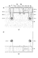
図1は、本発明の第1の実施の形態によるアンテナ装置1aの構成を示す斜視図である。図1に示すように、アンテナ装置1aは、表面実装型アンテナ10と、表面実装型アンテナ10が設置される基板20とを備えて構成される。図2には表面実装型アンテナ10の展開図を、図3には基板20の構成を示す平面図をそれぞれ示している。図3(a)は基板20のおもて面(表面実装型アンテナ10が設置される面)の平面図であり、図3(b)は基板20のうら面の平面図である。なお、アンテナ装置1aは、携帯電話などの小型の無線通信機に搭載されるものである。
[First Embodiment]
FIG. 1 is a perspective view showing a configuration of an antenna device 1a according to the first embodiment of the present invention. As shown in FIG. 1, the antenna device 1a includes a surface-mounted
図1及び図2に示すように、表面実装型アンテナ10は、略直方体形状の誘電体からなる基体11と、基体11の表面上の導体により構成されるアンテナ素子13(第1のアンテナ素子)及びアンテナ素子14(第2のアンテナ素子)とを備える。この表面実装型アンテナ10は、図1に示すように基板20の角部近傍に設置される。
As shown in FIGS. 1 and 2, the surface-mounted
なお、「略直方体形状」とは、完全な直方体だけでなく一部不完全な直方体を含む意である。本実施の形態では、基体11は上面11Cに他の部分より高さhだけ突出する凸面12を有しており、完全な直方体形状とはなっていない。
The “substantially rectangular parallelepiped shape” means not only a complete rectangular parallelepiped but also a partially incomplete rectangular parallelepiped. In the present embodiment, the
基体11の大きさは、目的とするアンテナ特性に応じて適宜設定すればよい。特に限定されるものではないが、横方向の長さx1,x2(x1>x2)をそれぞれ14mm,3mmとし、高さx3を3mmとすることができる。また、基体11の材料としては、特に限定されるものではないが、Ba−Nd−Ti系材料(比誘電率80〜120)、Nd−Al−Ca−Ti系材料(比誘電率43〜46)、Li−Al−Sr−Ti(比誘電率38〜41)、Ba−Ti系材料(比誘電率34〜36)、Ba−Mg−W系材料(比誘電率20〜22)、Mg−Ca−Ti系材料(比誘電率19〜21)、サファイヤ(比誘電率9〜10)、アルミナセラミックス(比誘電率9〜10)、コージライトセラミックス(比誘電率4〜6)などの誘電体材料を用いることが好適である。基体11は、金型を用いてこれらの材料を焼成することによって作製される。
What is necessary is just to set the magnitude | size of the base |
具体的に用いる誘電体材料は、後述するアンテナ素子13,14の使用目的である無線通信方式の使用周波数に応じて適宜選択すればよい。なお、比誘電率εrが大きいほど大きな波長短縮効果が得られ、放射導体の長さをより短くすることができるが、比誘電率εrが大きすぎるとアンテナ利得が減少してしまう。そこで、これらのバランスを見ながら、最適な誘電体材料を決定することが好ましい。一例を挙げると、アンテナ素子13の使用目的をGPS受信とし、アンテナ素子14の使用目的をIEEE802.11bの無線LAN通信とする場合、比誘電率が5〜40程度の誘電体材料を用いることが好ましい。このような誘電体材料としては、Mg−Ca−Ti系誘電体セラミックを好ましく挙げることができる。Mg−Ca−Ti系誘電体セラミックとしては、TiO2、MgO、CaO、MnO、SiO2を含有するMg−Ca−Ti系誘電体セラミックを用いることが特に好ましい。
The dielectric material to be specifically used may be appropriately selected according to the use frequency of the wireless communication system that is the purpose of use of the
アンテナ素子13は、基体11の上面11Cに形成される放射電極13A(第1の放射電極)と、側面11A(長手方向に垂直な側面)から底面11Eにわたって連続して形成される導体13Bと、側面11B(長手方向に平行な側面)から基体11の底面11Eにわたって連続して形成される導体13Cと、側面11Aに形成される給電電極13D(第1の給電電極)と、側面11Bに形成される導体13E(第1の導体)とによって構成される。また、アンテナ素子14は、基体11の上面11Cに形成される放射電極14A(第2の放射電極)と、側面11F(側面11Aに向かい合う側面)から底面11Eにわたって連続して形成される導体14Bと、底面11Eに形成される導体14Cと、側面11Fに形成される給電電極14D(第2の給電電極)と、側面11D(側面11Bに向かい合う側面)に形成される導体14E(第2の導体)とによって構成される。なお、これらの電極及び導体はいずれもスクリーン印刷によって形成することが好適である。
The
放射電極13A,14Aは、上面11Cに設けられた凸面12上に、基体11の長手方向の一端(側面11F側の端部)から他端に向かって互いに平行に延設される。凸面12は、側面11Bとの境界に沿う一定幅w1の凸面と、側面11Dとの境界に沿う一定幅w2の凸面とを含んでおり、放射電極13Aは、このうち一定幅w1の凸面上の全面に形成される。したがって、放射電極13Aは、幅がw1に等しく、長さが基体11の長手方向の全長に等しい矩形状の導体パターンとなっている。一方、放射電極14Aは一定幅w2の凸面のうち、基体11の上記一端(側面11F側の端部)から、基体11の長手方向の全長より短い所定距離L1(<x1)の部分のみに形成される。したがって、放射電極13Aは、幅がw2に等しく、長さがL1である矩形状の導体パターンとなっている。
The
導体13B,14Bは、底面11Eの長手方向の側面11A側端部及び側面11F側端部に、底面11Eの全幅にわたってそれぞれ形成された矩形状の導体パターンであり、それぞれ側面11A及び11Fの底面11Eとの境界付近にも延設されている。
The
導体13C,14Cは、導体14Bと導体13Bの間にこの順で設けられる矩形状の導体パターンである。導体13Cは、底面11Eの全幅にわたって形成されるとともに、側面11Bの底面11Eとの境界付近にも延設されている。一方、導体14Cは、底面11Eの全幅にわたって形成されることはなく、側面11Dとの境界付近に一定の幅で形成される。
The
導体15は、導体14Cが底面11Eの全幅にわたって形成されないことで生まれた領域に形成される矩形状の導体パターンである。導体15は基体11表面の他の導体とは接触していない。
The
給電電極13Dは、側面11A上に側面11Bとの境界に沿って一定幅w1で形成される。給電電極13Dの上端は放射電極13Aに接触しており、下端は導体13Bに接触している。給電電極14Dは、側面11F上に側面11Dとの境界に沿って一定幅w2で形成される。給電電極14Dの上端は放射電極14Aに接触しているが、下端は導体14Bには接触せず、導体14Bとの間に所定幅のギャップ14gが設けられている。給電電極14Dの上下方向の長さはL2に設定する。また、給電電極14Dは、ギャップ14gに沿い、側面11Bに向かって端部14Daまで長さL3分だけ延設されている。
The feeding
導体13Eは側面11B上に設けられるが、側面11Fとの境界に沿って側面11Bの上下方向中央付近まで一定幅w1で形成された部分13E−1と、部分13E−1の下端から側面11Bの中央付近の端部13Eaまで一定幅w1で形成された長さL4の部分13E−2とから構成される。部分13E−2と導体13Cとは接触しておらず、その間には所定幅のギャップ13gが設けられている。導体14Eは、側面11D上を上から下に向かって設けられる矩形状の導体パターンである。導体14Eの幅は、放射電極14Aの幅と同じw2となっている。導体14Eの上端は放射電極14Aと接触し、下端は導体14Cと接触している。
The
次に、図1及び図3に示すように、基板20は、おもて面に、グランドパターンの設けられていないグランドクリアランス領域21と、グランドクリアランス領域21の周囲に設けられたグランドパターン22(第1のグランドパターン)と、グランドクリアランス領域21内に設けられたランドパターン23−1〜2,24−1〜2,25と、ランドパターン23−1,2にそれぞれ接続する給電ライン26−1,2と、給電ライン26−1,2を基板20のうら面に誘導するスルーホール導体27−1,2とを有し、うら面に、グランドパターン29(第2のグランドパターン)を有している。なお、グランドクリアランス領域21の破線で示す領域Xは、表面実装型アンテナ10の設置領域である。図示していないが、基板20には無線通信機を構成するための他の様々な電子部品も実装される。
Next, as shown in FIGS. 1 and 3, the
グランドクリアランス領域21は、基板20の角部に沿って設けられている。そのため、グランドクリアランス領域21の周囲2方向はグランドパターン22に囲まれているが、他の2方向は基板20の存在しない開放空間である。
The
うら面のグランドパターン29は、領域Xの直下にも存在している。これにより、表面実装型アンテナ10は所謂オングランドタイプとなっている。
The
ランドパターン23−1,2はそれぞれ、表面実装型アンテナ10の導体13B,14Bに対応する位置に設けられ、これらの導体と半田接続される。なお、ランドパターン23−1は端部23−1aでグランドパターン22と接触しており、これにより給電ライン26−1とグランドパターン22とが接続している。また、ランドパターン24−1,2はそれぞれ、表面実装型アンテナ10の導体13C,14Cに対応する位置に設けられ、これらの導体と半田接続される。また、ランドパターン25は、表面実装型アンテナ10の導体15に対応する位置に設けられ、導体15と半田接続される。
The land patterns 23-1 and 23-2 are provided at positions corresponding to the
給電ライン26−1,2はそれぞれランドパターン23−1,2に接続しており、給電ライン26−1,2とグランドパターン22との間にはそれぞれインピーダンス調整用のチップリアクタ28a,28bが実装されている。チップリアクタ28a,28bの実装位置は、グランドクリアランス領域21の外側であって、グランドクリアランス領域21にできるだけ近い位置が好ましい。なお、給電ライン26−1,2はスルーホール導体27−1,2によってうら面に導入され、うら面で信号ライン(不図示)に接続されている。
The feeder lines 26-1 and 26-2 are connected to the land patterns 23-1 and 23-2, respectively. Between the feeder lines 26-1 and 26 and the
ランドパターン24−1,2とグランドパターン22との間にはそれぞれ周波数調整用のチップリアクタ28c,28dが実装されている。チップリアクタ28c,28dはそれぞれ、ランドパターン24−1,2のリード部分24−1a,2aとグランドパターン22との間に直列に挿入されている。チップリアクタ28c,28cの実装位置も、グランドクリアランス領域21の外側であって、グランドクリアランス領域21にできるだけ近い位置が好ましい。
Between the land patterns 24-1 and 2 and the
なお、チップリアクタ28dは、インダクタ、キャパシタ、若しくはショートである必要がある。後述するように、アンテナ素子14では導体14C及び導体14Eをショートスタブとして機能させることになるが、これは、導体14C及び導体14Eがグランドパターン22に接続していることによって実現されるものであるからである。
The
ランドパターン25は基板20の他のパターン等と接続しておらず、フローティング状態となっている。
The
表面実装型アンテナ10と基板20とが以上説明したような構成を有することにより、アンテナ素子13及び14はそれぞれ逆Fアンテナとして機能する。すなわち、まずアンテナ素子13では、給電電極13D及び導体13Bが逆Fアンテナのショートスタブとして機能し、導体13Eのギャップ13g側の端部13Eaが逆Fアンテナの開放端として機能する。また、アンテナ素子14では、導体14E及び導体14Cが逆Fアンテナのショートスタブとして機能し、導体14Dのギャップ14g側の端部14Daが逆Fアンテナの開放端として機能する。
Since the
アンテナ素子13,14の共振周波数は、主として基体11の表面に形成した導体の長さ及び幅並びに基体11の比誘電率等によって決定される。しかし、アンテナ装置1aでは、チップリアクタ28c,28dのリアクタンスを適宜調整することにより、共振周波数の微調整も可能になっている。
The resonance frequencies of the
ここで、相対的に基板20の外側に位置するアンテナ素子13は、相対的に低い周波数の無線通信方式用に用い、相対的に基板20の内側に位置するアンテナ素子14は、相対的に高い周波数の無線通信方式用に用いることが好ましい。一例を挙げると、例えば1.5GHz帯の周波数を用いるGPS受信と、2.5GHz帯の周波数を用いるIEEE802.11b通信とに対応させる場合、アンテナ素子13の共振周波数を1.5GHz帯に調整し、アンテナ素子14の共振周波数を2.5GHz帯に調整することが好ましい。
Here, the
さて、表面実装型アンテナ10は、放射電極13A及び14Aの給電方法に特徴を有する。すなわち、放射電極13Aは直接給電され、放射電極14Aは容量結合給電される。ここで、直接給電とは、放射電極と基板20上の給電ラインとが連続した一連の導体によって接続されていること(直接接続)を意味し、容量結合給電とは、放射電極と基板上の給電ラインとがギャップを介して接続されていること(容量結合接続)を意味する。
Now, the
具体的には、給電ライン26−1、ランドパターン23−1、導体13B、給電電極13D、及び放射電極13Aが一連の連続した導体となっていることにより、放射電極13Aの直接給電が実現されている。また、給電ライン26−2、ランドパターン23−2、導体14B、給電電極14D、及び放射電極14Aが、途中にギャップ14gを有する点を除き、一連の連続した導体となっていることにより、放射電極14Aの容量結合給電が実現されている。
Specifically, the power supply line 26-1, the land pattern 23-1, the
以上のような給電方法を用いることにより、放射電極14Aに流れる電流は、放射電極13Aに流れる電流に比べて位相が90°進むことになる。そのため、アンテナ素子13とアンテナ素子14との間での電磁界の干渉が減少する。したがって、両方の放射電極について同じ給電方法を用いる場合に比べると、放射電極13Aと放射電極14Aを近づけることができるので、小型化されたコンボアンテナタイプの表面実装型アンテナを提供可能になる。
By using the above feeding method, the phase of the current flowing through the
図4は、本実施の形態による表面実装型アンテナ10の特性(実施例1)と、表面実装型アンテナ10からギャップ14gをなくし、かつ導体14Eと導体14Cを切り離した例(比較例1)の特性との比較を示すグラフであり、横軸は周波数、縦軸は給電ライン26−1から信号を入力した場合に給電ライン26−2から出力される信号の振幅の比率(「S21値」という。)を示している。このグラフでは、値が小さいほどアンテナ素子13とアンテナ素子14との間での電磁界の干渉が小さいことが示される。
FIG. 4 shows characteristics of the
図10及び図11に、比較例1によるアンテナ装置1cの構成を示す斜視図と、比較例1による表面実装型アンテナ10の展開図を示しておく。これらの図に示すように、比較例1では、ギャップ14gがなくなって導体14Bと給電電極14Dとが接触し、導体14Cと導体14Eの間にギャップ14hが設けられてこれらが切り離されている。なお、このようにしたことにより、実施例1と比較例1とでは、アンテナ素子14のショートスタブと開放端が互いに逆になっている。すなわち、アンテナ素子14では、導体14Eのギャップ14h側の端部14Eaが逆Fアンテナの開放端として機能し、導体14D及び導体14Bが逆Fアンテナのショートスタブとして機能する。
10 and 11 are a perspective view showing a configuration of the
なお、図4の特性を測定するにあたっては、最も良い特性が得られるよう、各部の長さ等を調整した。具体的には、x1=14mm、x2=3mm、x3=3mm、w1=1mm、w2=1mm、L1=11.4mm、L2=2.2mm、L3=1.0mm、L4=8.9mm、h=0.2mm、ギャップ13g,14g,14hの各幅をそれぞれ0.4mm,0.3mm,1.0mmとした。
In measuring the characteristics shown in FIG. 4, the length of each part was adjusted so that the best characteristics could be obtained. Specifically, x1 = 14 mm, x2 = 3 mm, x3 = 3 mm, w1 = 1 mm, w2 = 1 mm, L1 = 11.4 mm, L2 = 2.2 mm, L3 = 1.0 mm, L4 = 8.9 mm, h = 0.2 mm, and the widths of the
図4に示すように、実施例1のS21値は、アンテナ素子13,14の共振周波数帯を含む測定周波数の全範囲(1〜3GHz)で比較例1よりも小さくなっていた。このことから、実施例1では、比較例1に比べてアンテナ素子13とアンテナ素子14との間での電磁界の干渉が小さくなっていることが理解される。
As shown in FIG. 4, the S21 value of Example 1 was smaller than that of Comparative Example 1 over the entire measurement frequency range (1 to 3 GHz) including the resonance frequency bands of the
以上説明したように、表面実装型アンテナ10及びこれを用いるアンテナ装置1aでは、放射電極13Aを直接給電し、放射電極14Aを容量結合給電することにより、アンテナ素子13とアンテナ素子14との間での電磁界の干渉が従来より小さくなっている。したがって、放射電極13Aと放射電極14Aをより近づけることができるので、小型化されたコンボアンテナタイプの表面実装型アンテナを提供可能になる。
As described above, in the surface-mounted
他にも、表面実装型アンテナ10では、アンテナ素子13及び14の各開放端(端部13Ea及び14Da)が、基体11の90°の角度をなす2つの面(側面11B及び11F)にそれぞれ形成されることになる。このことにより、アンテナ素子13及び14の各アンテナ特性が向上している。
In addition, in the surface-mounted
また、表面実装型アンテナ10では、アンテナ素子13及び14の各ショートスタブ(アンテナ素子13では給電電極13D及び導体13B。アンテナ素子14では導体14E及び14C。)を、ともに基板20の角部側に寄せることが可能になっている。逆Fアンテナは、ショートスタブを介して基板に生成される影像を利用するアンテナであるが、表面実装型アンテナ10では、アンテナ素子13及び14のショートスタブがともに基板20の角部に位置することで、アンテナ素子13及び14ともに効率のよい影像生成が実現される。したがって、アンテナ素子13及び14のアンテナ効率が向上する。
In the surface-mounted
また、基体11の上面11Cに、放射電極を形成するための凸面12を設けたことで、スクリーン印刷によって各放射電極を形成する際の位置ずれを防止できる。また、放射電極間が相対的に凹んでいることから、基体11の体積を減らすことができ、アンテナ特性が向上するとともに、アンテナ素子13とアンテナ素子14との間での電磁界の干渉が減少するという効果も奏される。
Further, by providing the
[第2の実施の形態]
図5は、本発明の第2の実施の形態によるアンテナ装置1bの構成を示す斜視図である。図6にはアンテナ装置1bを構成する表面実装型アンテナ10の展開図を、図7にはアンテナ装置1bを構成する基板20の構成を示す平面図をそれぞれ示している。図7(a)は基板20のおもて面の平面図であり、図7(b)は基板20のうら面の平面図である。
[Second Embodiment]
FIG. 5 is a perspective view showing a configuration of an
アンテナ装置1bは、アンテナ装置1aにおいて、基体11上の各導体に流れる電流をグランドに強制的に誘導することで、アンテナ素子13とアンテナ素子14との間での電磁界の干渉をより小さくしようとするものである。これを、設置領域X内に、グランド電位とした複数のランドパターンを設けることで実現する。
In the
具体的には、まず図5及び図7に示すように、基板20おもて面に、他のパターン等と接続しないフローティング状態のランドパターン25を多数設ける。なお、ランドパターン25を設置するためのスペースは、ランドパターン23−1,2及び24−1,2の面積を縮小することで確保する。そして、各ランドパターン25とうら面のグランドパターン29とをスルーホール導体30で接続する。なお、スルーホール導体30は各ランドパターン25の中央付近に設けることが好ましい。
Specifically, first, as shown in FIGS. 5 and 7, a large number of floating
ランドパターン25をグランド電位にするために、上記のようにスルーホール導体30を用いることで、おもて面の配線が複雑になることを防止できるが、可能な場合にはスルーホール導体30を用いずに、おもて面のグランドパターン22と直接接続することとしてもよい。図7には、このようにして設けたランドパターンの例も示している。すなわち、図7の例では、グランドパターン22の一部をグランドクリアランス領域21内まで延伸している(延伸部分22a)。このようにした場合、延伸部分22aがグランド電位のランドパターンのひとつとして機能する。
By using the through-
また、グランドパターン22とグランドパターン29とを、スルーホール導体30により接続してもよい。この場合、図5及び図7に示すように、特にランドパターン23−1とグランドパターン22の接触部近辺にスルーホール導体30を設けることが好適である。
Further, the
図8は、アンテナ装置1bの表面実装型アンテナ10付近を、基板20側面の4方向から見た略透視図である。図8(a),図8(b),図8(c),図8(d)はそれぞれ、図7(a)に示した方向A,方向B,方向C,方向Dに対応している。なお、図8では、スルーホール導体30のみを透視図で示し、その他の構成については平面図としている。図8に示すように、スルーホール導体30は基板20を貫き、おもて面のパターンとうら面のパターンとを電気的に接続している。
FIG. 8 is a schematic perspective view of the vicinity of the surface-mounted
一方、表面実装型アンテナ10の側では、図5及び図6に示すように、各ランドパターン25に対応する位置に、基体11表面の他の導体とは接触しない導体15を設ける。導体15とランドパターン25とは半田接続する。このようにするのは、基体11の表面電位を確実にグランド電位とするためである。ただし、製造の都合上、スルーホール導体30の位置には導体15を設けないほうが好ましい。
On the other hand, on the surface-mounted
以上のように、アンテナ装置1bでは、グランド電位とした複数のランドパターン25を設置領域X内に設けたことで、アンテナ素子13とアンテナ素子14との間での電磁界の干渉をさらに減少させることが可能になる。
As described above, in the
図9は、本実施の形態による表面実装型アンテナ10の特性(実施例2)と、図4にも示した第1の実施の形態による表面実装型アンテナ10の特性(実施例1)との比較を示すグラフである。横軸及び縦軸などは図4と同様である。
FIG. 9 shows the characteristics of the
なお、実施例2の特性を測定するにあたっても、最も良い特性が得られるよう、各部の長さ等を調整した。具体的には、x1=14mm、x2=3mm、x3=3mm、w1=1.0mm、w2=0.5mm、L1=10.2mm、L2=2.2mm、L3=1.0mm、L4=6.2mm、L5=12.0mm、h=0.2mm、ギャップ13g,14gの各幅をそれぞれ0.5mm,0.3mmとした。また、導体14Dのギャップ14gに沿った延設部分の太さw3をw2より太くし、1.3mmとした。さらに、図6に示すように、導体13Eの折れ曲がり部付近に切り欠き13Ebを設けた。また、導体13Cのうち側面11B上に形成されている部分を取り除いた。また、放射電極13Aの一部(側面11Fから長さL5(<x1)=1.0mmの部分)の幅w3をw1より細くし、0.9mmとした。これは、凸面12の一部の幅を細くすることで実現している。
In measuring the characteristics of Example 2, the length of each part was adjusted so that the best characteristics were obtained. Specifically, x1 = 14 mm, x2 = 3 mm, x3 = 3 mm, w1 = 1.0 mm, w2 = 0.5 mm, L1 = 10.2 mm, L2 = 2.2 mm, L3 = 1.0 mm, L4 = 6 0.2 mm, L5 = 12.0 mm, h = 0.2 mm, and the widths of the
図9に示すように、実施例2のS21値は、アンテナ素子13,14の共振周波数帯を含む測定周波数の全範囲(1〜3GHz)で実施例1よりも小さくなっていた。このことから、実施例2では、実施例1に比べてさらに、アンテナ素子13とアンテナ素子14との間での電磁界の干渉が小さなっていることが理解される。
As shown in FIG. 9, the S21 value of Example 2 was smaller than that of Example 1 over the entire measurement frequency range (1 to 3 GHz) including the resonance frequency bands of the
なお、スルーホール導体30及びランドパターン25の数や位置は、最も良い特性が得られるよう、実験により決定されるものである。本実施の形態で示したスルーホール導体30及びランドパターン25の数や位置は、現在進めている実験によれば最適と考えられるものであるが、実験結果は様々な要因によって変化し得るので、本実施の形態で示したスルーホール導体30及びランドパターン25の数や位置が絶対的に最適なものであるわけではない。したがって、スルーホール導体30及びランドパターン25の数や位置は、本実施の形態で示したもの以外にも様々な態様を取り得る。
The numbers and positions of the through-
以上、本発明の好ましい実施の形態について説明したが、本発明はこうした実施の形態に何等限定されるものではなく、本発明が、その要旨を逸脱しない範囲において、種々なる態様で実施され得ることは勿論である。 As mentioned above, although preferable embodiment of this invention was described, this invention is not limited to such embodiment at all, and this invention can be implemented in various aspects in the range which does not deviate from the summary. Of course.
1a〜1c アンテナ装置
10 表面実装型アンテナ
11 基体
12 凸面
13,14 アンテナ素子
13A,14A 放射電極
13B,14B,13C,14C,13E,14E,15 導体
13D,14D 給電電極
13g,14g,14h ギャップ
20 基板
21 グランドクリアランス領域
22,29 グランドパターン
23,24,25 ランドパターン
26 給電ライン
27,30 スルーホール導体
28a〜28d チップリアクタ
1a to
Claims (9)
前記上面に形成される第1の放射電極と、前記第1の側面に形成される第1の給電電極と、前記第3の側面に形成される第1の導体とを有する第1の逆Fアンテナ素子と、
前記上面に形成される第2の放射電極と、前記第2の側面に形成される第2の給電電極と、前記第4の側面に形成される第2の導体とを有する第2の逆Fアンテナ素子とを備え、
当該表面実装型アンテナが設置される基板には、第1及び第2の給電ラインと、第1のグランドパターンとが形成され、
前記第1の放射電極は、前記上面と前記第1の側面との境界で前記第1の給電電極と接触するとともに、前記上面と前記第3の側面との境界で前記第1の導体と接触し、
前記第1の給電電極は、前記第1の給電ラインと直接接続されて前記第1の放射電極に直接給電を行うとともに、前記第1のグランドパターンと接続されて前記第1の逆Fアンテナのショートスタブを構成し、
前記第1の導体は、前記第1の逆Fアンテナの開放端を構成し、
前記第2の放射電極は、前記上面と前記第2の側面との境界で前記第2の給電電極と接触するとともに、前記上面と前記第4の側面との境界で前記第2の導体と接触し、
前記第2の給電電極は、ギャップを介して前記第2の給電ラインと接続されて前記第2の放射電極に容量結合給電を行うとともに、前記ギャップに対向する端部が前記第2の逆Fアンテナの開放端を構成し、
前記第2の導体は、前記第1のグランドパターンと接続されて前記第2の逆Fアンテナのショートスタブを構成し、
前記第2の導体は、前記第4の側面のうち前記第1の側面寄りの部分に形成されることを特徴とする表面実装型アンテナ。 A top surface, a bottom surface, a first side surface perpendicular to the longitudinal direction, a second side surface facing the first side surface, a third side surface parallel to the longitudinal direction, and a fourth side surface facing the third side surface. A substantially rectangular parallelepiped base;
A first radiation electrode formed on the upper surface, a first feeding electrode formed on the first side surface, a first inverse and a first conductor formed on the third side face An F antenna element;
A second radiation electrode formed on the upper surface, the second feeding electrode formed on the second side surface, a second reverse and a second conductor formed on said fourth side F antenna element ,
On the substrate on which the surface mount antenna is installed, the first and second feeding lines and the first ground pattern are formed,
The first radiation electrode is in contact with the first feeding electrode at a boundary between the upper surface and the first side surface, and is in contact with the first conductor at a boundary between the upper surface and the third side surface. And
The first power supply electrode is directly connected to the first power supply line to directly supply power to the first radiation electrode, and is connected to the first ground pattern to be connected to the first inverted F antenna. Configure the short stub,
The first conductor constitutes an open end of the first inverted F antenna;
The second radiation electrode is in contact with the second power feeding electrode at a boundary between the upper surface and the second side surface, and is in contact with the second conductor at a boundary between the upper surface and the fourth side surface. And
The second power supply electrode is connected to the second power supply line through a gap to perform capacitive coupling power supply to the second radiation electrode, and an end facing the gap has the second reverse F. Configure the open end of the antenna,
The second conductor is connected to the first ground pattern to form a short stub of the second inverted F antenna;
Said second conductor, said fourth surface-mounted antenna according to claim Rukoto formed in a portion of the first side closer among the side surfaces.
前記第1及び第2の放射電極は前記凸面に設けられることを請求項1乃至3のいずれか一項に記載の表面実装型アンテナ。 Said substrate has a convex surface projecting from the other part on the upper surface,
The surface mount antenna according to any one of claims 1 to 3 , wherein the first and second radiation electrodes are provided on the convex surface.
うら面に設けられた第2のグランドパターンと、
前記第2のグランドパターンとおもて面とを接続する複数のスルーホール導体とを有し、
前記複数のランドパターンは、それぞれ前記複数のスルーホール導体のいずれかによって前記第2のグランドパターンと接続されることを特徴とする請求項7に記載のアンテナ装置。 The substrate is
A second ground pattern provided on the back surface;
A plurality of through-hole conductors connecting the second ground pattern and the front surface;
The antenna device according to claim 7, wherein each of the plurality of land patterns is connected to the second ground pattern by any one of the plurality of through-hole conductors.
Priority Applications (3)
| Application Number | Priority Date | Filing Date | Title |
|---|---|---|---|
| JP2008276706A JP4784636B2 (en) | 2008-10-28 | 2008-10-28 | Surface mount antenna, antenna device using the same, and radio communication device |
| EP09013523A EP2182578A1 (en) | 2008-10-28 | 2009-10-27 | Surface-mounted antenna, antenna device using the same, and radio communication equipment |
| US12/607,229 US8384598B2 (en) | 2008-10-28 | 2009-10-28 | Surface-mounted antenna, antenna device using the same, and radio communication equipment |
Applications Claiming Priority (1)
| Application Number | Priority Date | Filing Date | Title |
|---|---|---|---|
| JP2008276706A JP4784636B2 (en) | 2008-10-28 | 2008-10-28 | Surface mount antenna, antenna device using the same, and radio communication device |
Publications (2)
| Publication Number | Publication Date |
|---|---|
| JP2010109434A JP2010109434A (en) | 2010-05-13 |
| JP4784636B2 true JP4784636B2 (en) | 2011-10-05 |
Family
ID=41328962
Family Applications (1)
| Application Number | Title | Priority Date | Filing Date |
|---|---|---|---|
| JP2008276706A Expired - Fee Related JP4784636B2 (en) | 2008-10-28 | 2008-10-28 | Surface mount antenna, antenna device using the same, and radio communication device |
Country Status (3)
| Country | Link |
|---|---|
| US (1) | US8384598B2 (en) |
| EP (1) | EP2182578A1 (en) |
| JP (1) | JP4784636B2 (en) |
Families Citing this family (7)
| Publication number | Priority date | Publication date | Assignee | Title |
|---|---|---|---|---|
| JP5375719B2 (en) * | 2010-04-01 | 2013-12-25 | Tdk株式会社 | ANTENNA DEVICE AND RADIO COMMUNICATION DEVICE USING THE SAME |
| GB201100617D0 (en) * | 2011-01-14 | 2011-03-02 | Antenova Ltd | Dual antenna structure having circular polarisation characteristics |
| JP5711318B2 (en) * | 2013-08-05 | 2015-04-30 | Tdk株式会社 | ANTENNA DEVICE AND RADIO COMMUNICATION DEVICE USING THE SAME |
| CN104347959A (en) * | 2013-08-09 | 2015-02-11 | 无锡村田电子有限公司 | Antenna device |
| WO2019008913A1 (en) * | 2017-07-06 | 2019-01-10 | 株式会社村田製作所 | Antenna module |
| KR102501224B1 (en) * | 2021-06-30 | 2023-02-21 | 주식회사 에이스테크놀로지 | Omni-Directional MIMO Antenna |
| FR3126053A1 (en) * | 2021-08-06 | 2023-02-10 | Axem Technology | RFID identifier and process for producing this identifier |
Family Cites Families (10)
| Publication number | Priority date | Publication date | Assignee | Title |
|---|---|---|---|---|
| CA2426497C (en) * | 1999-09-09 | 2005-06-28 | Murata Manufacturing Co., Ltd. | Surface-mount antenna and communication device with surface-mount antenna |
| EP1162688A4 (en) * | 1999-09-30 | 2005-04-13 | Murata Manufacturing Co | Surface-mount antenna and communication device with surface-mount antenna |
| JP3658639B2 (en) * | 2000-04-11 | 2005-06-08 | 株式会社村田製作所 | Surface mount type antenna and radio equipped with the antenna |
| JP2002335117A (en) * | 2001-05-08 | 2002-11-22 | Murata Mfg Co Ltd | Antenna structure and communication device equipped therewith |
| JP2003249811A (en) * | 2001-12-20 | 2003-09-05 | Murata Mfg Co Ltd | Double-resonance antenna apparatus |
| JP4301034B2 (en) * | 2004-02-26 | 2009-07-22 | パナソニック株式会社 | Wireless device with antenna |
| JP4284252B2 (en) | 2004-08-26 | 2009-06-24 | 京セラ株式会社 | Surface mount antenna, antenna device using the same, and radio communication device |
| KR100799875B1 (en) * | 2006-11-22 | 2008-01-30 | 삼성전기주식회사 | Chip antenna and mobile-communication terminal comprising the same |
| JP4793701B2 (en) * | 2007-01-19 | 2011-10-12 | 株式会社村田製作所 | ANTENNA DEVICE AND RADIO COMMUNICATION DEVICE |
| JP5093230B2 (en) * | 2007-04-05 | 2012-12-12 | 株式会社村田製作所 | Antenna and wireless communication device |
-
2008
- 2008-10-28 JP JP2008276706A patent/JP4784636B2/en not_active Expired - Fee Related
-
2009
- 2009-10-27 EP EP09013523A patent/EP2182578A1/en not_active Withdrawn
- 2009-10-28 US US12/607,229 patent/US8384598B2/en not_active Expired - Fee Related
Also Published As
| Publication number | Publication date |
|---|---|
| US8384598B2 (en) | 2013-02-26 |
| EP2182578A1 (en) | 2010-05-05 |
| JP2010109434A (en) | 2010-05-13 |
| US20100103057A1 (en) | 2010-04-29 |
Similar Documents
| Publication | Publication Date | Title |
|---|---|---|
| JP4189306B2 (en) | Dielectric antenna and electric device having communication function using the same | |
| US6680700B2 (en) | Miniaturized microwave antenna | |
| US7642970B2 (en) | Antenna device and wireless communication apparatus using same | |
| JP4784636B2 (en) | Surface mount antenna, antenna device using the same, and radio communication device | |
| JP5333235B2 (en) | ANTENNA DEVICE AND RADIO COMMUNICATION DEVICE USING THE SAME | |
| JP5546587B2 (en) | Antenna device | |
| JP2002299933A (en) | Electrode structure for antenna and communication equipment provided with the same | |
| KR20120105004A (en) | Antenna | |
| JP2001358517A (en) | Antenna device and radio equipment using the same | |
| JP2008294491A (en) | Antenna system | |
| JP2005094360A (en) | Antenna device and radio communication apparatus | |
| JP4645729B2 (en) | ANTENNA DEVICE, RADIO COMMUNICATION DEVICE, SURFACE MOUNTED ANTENNA, PRINTED BOARD, SURFACE MOUNTED ANTENNA AND PRINTED BOARD MANUFACTURING METHOD | |
| JP2015088874A (en) | Chip antenna device and transmitting/receiving communication circuit board | |
| JPH05259724A (en) | Print antenna | |
| JP4263972B2 (en) | Surface mount antenna, antenna device, and wireless communication device | |
| JP2011119949A (en) | Card device | |
| JPH10247806A (en) | Antenna for portable radio equipment and portable radio equipment using the antenna | |
| JP2009194783A (en) | Pattern antenna and antenna apparatus with pattern antenna mounted on master substrate | |
| JP2005229161A (en) | Antenna and radio communication equipment therewith | |
| KR20120014679A (en) | Antenna apparatus having device carrier with magneto-dielectric material | |
| JP4372325B2 (en) | antenna | |
| JP5251965B2 (en) | Antenna device and frequency adjustment method thereof | |
| WO2018021353A1 (en) | Antenna and wireless module | |
| JPH10256818A (en) | Antenna system and its mounting structure | |
| JP4894502B2 (en) | Antenna device |
Legal Events
| Date | Code | Title | Description |
|---|---|---|---|
| A977 | Report on retrieval |
Free format text: JAPANESE INTERMEDIATE CODE: A971007 Effective date: 20100702 |
|
| A131 | Notification of reasons for refusal |
Free format text: JAPANESE INTERMEDIATE CODE: A131 Effective date: 20100803 |
|
| A521 | Request for written amendment filed |
Free format text: JAPANESE INTERMEDIATE CODE: A523 Effective date: 20100930 |
|
| TRDD | Decision of grant or rejection written | ||
| A01 | Written decision to grant a patent or to grant a registration (utility model) |
Free format text: JAPANESE INTERMEDIATE CODE: A01 Effective date: 20110614 |
|
| A01 | Written decision to grant a patent or to grant a registration (utility model) |
Free format text: JAPANESE INTERMEDIATE CODE: A01 |
|
| A61 | First payment of annual fees (during grant procedure) |
Free format text: JAPANESE INTERMEDIATE CODE: A61 Effective date: 20110627 |
|
| R150 | Certificate of patent or registration of utility model |
Free format text: JAPANESE INTERMEDIATE CODE: R150 |
|
| FPAY | Renewal fee payment (event date is renewal date of database) |
Free format text: PAYMENT UNTIL: 20140722 Year of fee payment: 3 |
|
| LAPS | Cancellation because of no payment of annual fees |