JP4301034B2 - Wireless device with antenna - Google Patents
Wireless device with antenna Download PDFInfo
- Publication number
- JP4301034B2 JP4301034B2 JP2004051083A JP2004051083A JP4301034B2 JP 4301034 B2 JP4301034 B2 JP 4301034B2 JP 2004051083 A JP2004051083 A JP 2004051083A JP 2004051083 A JP2004051083 A JP 2004051083A JP 4301034 B2 JP4301034 B2 JP 4301034B2
- Authority
- JP
- Japan
- Prior art keywords
- antenna element
- antenna
- feeding point
- point
- frequency
- Prior art date
- Legal status (The legal status is an assumption and is not a legal conclusion. Google has not performed a legal analysis and makes no representation as to the accuracy of the status listed.)
- Expired - Fee Related
Links
Images
Classifications
-
- H—ELECTRICITY
- H01—ELECTRIC ELEMENTS
- H01Q—ANTENNAS, i.e. RADIO AERIALS
- H01Q21/00—Antenna arrays or systems
- H01Q21/30—Combinations of separate antenna units operating in different wavebands and connected to a common feeder system
-
- H—ELECTRICITY
- H01—ELECTRIC ELEMENTS
- H01Q—ANTENNAS, i.e. RADIO AERIALS
- H01Q1/00—Details of, or arrangements associated with, antennas
- H01Q1/12—Supports; Mounting means
- H01Q1/22—Supports; Mounting means by structural association with other equipment or articles
- H01Q1/24—Supports; Mounting means by structural association with other equipment or articles with receiving set
- H01Q1/241—Supports; Mounting means by structural association with other equipment or articles with receiving set used in mobile communications, e.g. GSM
- H01Q1/242—Supports; Mounting means by structural association with other equipment or articles with receiving set used in mobile communications, e.g. GSM specially adapted for hand-held use
- H01Q1/243—Supports; Mounting means by structural association with other equipment or articles with receiving set used in mobile communications, e.g. GSM specially adapted for hand-held use with built-in antennas
-
- H—ELECTRICITY
- H01—ELECTRIC ELEMENTS
- H01Q—ANTENNAS, i.e. RADIO AERIALS
- H01Q1/00—Details of, or arrangements associated with, antennas
- H01Q1/36—Structural form of radiating elements, e.g. cone, spiral, umbrella; Particular materials used therewith
- H01Q1/38—Structural form of radiating elements, e.g. cone, spiral, umbrella; Particular materials used therewith formed by a conductive layer on an insulating support
-
- H—ELECTRICITY
- H01—ELECTRIC ELEMENTS
- H01Q—ANTENNAS, i.e. RADIO AERIALS
- H01Q5/00—Arrangements for simultaneous operation of antennas on two or more different wavebands, e.g. dual-band or multi-band arrangements
- H01Q5/40—Imbricated or interleaved structures; Combined or electromagnetically coupled arrangements, e.g. comprising two or more non-connected fed radiating elements
-
- H—ELECTRICITY
- H01—ELECTRIC ELEMENTS
- H01Q—ANTENNAS, i.e. RADIO AERIALS
- H01Q9/00—Electrically-short antennas having dimensions not more than twice the operating wavelength and consisting of conductive active radiating elements
- H01Q9/04—Resonant antennas
- H01Q9/30—Resonant antennas with feed to end of elongated active element, e.g. unipole
- H01Q9/42—Resonant antennas with feed to end of elongated active element, e.g. unipole with folded element, the folded parts being spaced apart a small fraction of the operating wavelength
Landscapes
- Engineering & Computer Science (AREA)
- Computer Networks & Wireless Communication (AREA)
- Physics & Mathematics (AREA)
- Electromagnetism (AREA)
- Details Of Aerials (AREA)
- Support Of Aerials (AREA)
- Variable-Direction Aerials And Aerial Arrays (AREA)
- Waveguide Aerials (AREA)
- Transceivers (AREA)
Description
本発明は、携帯電話などの移動体通信に用いられる、アンテナが搭載された無線装置に関するものである。 The present invention relates to a radio apparatus equipped with an antenna, which is used for mobile communication such as a mobile phone.
近年、携帯電話を含めた移動体通信は音声通話や文字や動画などのデータ通信へのサービスが多様化し、性能の高い無線装置が要求されている。特に、電波を送受信する入口となるアンテナの性能が無線装置の性能を左右する大きな要因の一つともなり、高性能であるアンテナが搭載された無線装置が要望されている。 In recent years, mobile communication including cellular phones has diversified services for voice communication, data communication such as text and moving images, and high performance wireless devices are required. In particular, the performance of an antenna serving as an entrance for transmitting and receiving radio waves is one of the major factors affecting the performance of a wireless device, and a wireless device equipped with a high-performance antenna is desired.
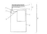
このような従来のアンテナが搭載された無線装置について、図3を用いて説明する。 A radio apparatus equipped with such a conventional antenna will be described with reference to FIG.
図3は従来のアンテナが搭載された無線装置を模式的に表した図であり、同図に示すように、地板8に対し並べて配置されているアンテナ3は、第1の周波数に共振する第1のアンテナ素子1、および第2の周波数に共振する第2のアンテナ素子2とを備えている。このアンテナ3は、地板8上に配置された給電点4に接続され、整合回路5、伝送線路6を介して無線回路7へと接続されており、それらを含めて無線装置9が構成されている。このように、当該無線装置9は、第1および第2のアンテナ素子1および2に、1つの給電点4から給電可能な構成とされていた。また、第1のアンテナ素子1は、GSM(880〜960MHz)に共振し、第2のアンテナ素子2は、前記第1のアンテナ素子1より高い周波数のDCS(1710〜1880MHz)に共振している。
FIG. 3 is a diagram schematically showing a radio apparatus equipped with a conventional antenna. As shown in FIG. 3, the antenna 3 arranged side by side with respect to the
以上の構成において、GSMを受信する時には、第1のアンテナ素子1で受信した電波により励起された電流が、給電点4から整合回路5、伝送線路6を介して無線回路7に伝達されることにより電波を受信する。
In the above configuration, when GSM is received, the current excited by the radio wave received by the first antenna element 1 is transmitted from the
また、GSMを送信する時には、無線回路7で発生した信号が、伝送線路6から整合回路5、給電点4を介して伝達される。その信号が第1のアンテナ素子1により励起されて電波として放射されることにより送信される。
When transmitting GSM, a signal generated in the
なお、DCSでも、GSMを送受信する時と同様の原理により第2のアンテナ素子2により電波の送受信が行われる。
In DCS, radio waves are transmitted and received by the
このように、無線装置9は、GSMとDCSと2つの周波数に対応するものであった。
Thus, the radio |
なお、この出願の発明に関連する先行技術文献情報としては、例えば、特許文献1が知られている。
しかしながら上記従来のアンテナが搭載された無線装置においては、1つの給電点4から第1のアンテナ素子1と第2のアンテナ素子2に給電可能な構成としてあるため、2つのアンテナ素子1および2の間の結合が強まりロスが生じやすい。
However, in the wireless device equipped with the conventional antenna, the first antenna element 1 and the
さらに、前記所望の異なる2つの共振周波数を得るための整合回路5も1つのみで調整を行うものであったため、一方側の共振周波数の調整を行うと他方側の共振周波数が連動して変化し、片方の共振周波数のみを独立して効率よく調整することが困難であった。
Further, since adjustment is performed with only one
本発明は、このような従来の課題を解決するものであり、2つのアンテナ素子の結合ロスを低減し、多周波でも任意に独立して所望の共振周波数に調整できるアンテナが搭載された無線装置を提供することを目的とする。 The present invention solves such a conventional problem, and reduces a coupling loss between two antenna elements, and a radio apparatus equipped with an antenna that can be arbitrarily adjusted to a desired resonance frequency even at multiple frequencies. The purpose is to provide.
上記目的を達成するために本発明は、以下の構成を有するものである。 In order to achieve the above object, the present invention has the following configuration.
本発明の請求項1に記載の発明は、第1の周波数に共振する第1のアンテナ素子および、前記第1の周波数より高い第2の周波数に共振する第2のアンテナ素子を備えたアンテナと、前記アンテナが搭載される無線装置内に配された地板とを有し、前記地板には、前記第1のアンテナ素子に接続されるように配置された第1の給電点と、前記第1の給電点に一端が接続された第1の整合回路と、前記第2のアンテナ素子に接続されるように配置された第2の給電点と、前記第2の給電点に一端が接続された第2の整合回路とを有し、さらに前記第1および第2の整合回路の他端が同じ接続点に接続され、その接続点に伝送線路を介して接続される無線回路を備えると共に、前記第2の整合回路は、前記第2の給電点と前記接続点との間に直列にコンデンサを挿入接続した構成とされ、前記第1の周波数の電波の送受信時に前記各アンテナ素子間の結合が少なくなるように前記第2のアンテナ素子と前記伝送線路との電気的な接続状態が前記コンデンサで低減される構成とされていることを特徴とする、アンテナが搭載された無線装置としたものである。 According to a first aspect of the present invention, an antenna and having a second antenna element that resonates to the first antenna element and a second frequency higher than said first frequency that resonates the first frequency , A ground plane disposed in a wireless device on which the antenna is mounted, the ground plane having a first feeding point arranged to be connected to the first antenna element, and the first A first matching circuit having one end connected to the feed point, a second feed point arranged to be connected to the second antenna element, and one end connected to the second feed point and a second matching circuit, together with further the other end of the first and second matching circuits are connected to the same connection point, and a radio circuit connected via a transmission line to the connection point, wherein The second matching circuit is connected in series between the second feeding point and the connection point. The capacitor is inserted and connected, and the electrical connection state between the second antenna element and the transmission line is reduced so that the coupling between the antenna elements is reduced during transmission and reception of the first frequency radio wave. A wireless device equipped with an antenna is characterized in that it is configured to be reduced by a capacitor .
この構成であれば、第1のアンテナ素子と第2のアンテナ素子にそれぞれ対応する独立した給電点を設けることで2つのアンテナ素子間の結合ロスを低減させることができ、しかも、2つのアンテナ素子に対しそれぞれ独立した整合回路を設けてあるため、任意に独立して2つの異なる共振周波数の調整が容易に行えるものにできるという作用を有する。 With this configuration, it is possible to reduce the coupling loss between the two antenna elements by providing independent feeding points respectively corresponding to the first antenna element and the second antenna element. In contrast, since independent matching circuits are provided, it is possible to easily adjust two different resonance frequencies independently of each other.
請求項2に記載の発明は、請求項1記載の発明において、第2の整合回路を、第2の給電点と接続点との間に直列に接続されたコンデンサに加え、前記第2の給電点と地板との間に直列に接続されたインダクタとにより構成されたものとしたものであり、請求項1記載の発明による作用に加えて、第1の周波数に共振する時、インダクタにより第2のアンテナ素子が地板と電気的に接続され、第2のアンテナ素子が無給電素子として機能するようにできる。この結果、第1のアンテナ素子と無給電素子として機能する第2のアンテナ素子との複共振により、第1の共振周波数が広帯域なものにできるという作用を有する。 According to a second aspect of the present invention, in the first aspect of the invention, the second matching circuit is added to a capacitor connected in series between the second feeding point and the connection point, and the second feeding circuit is added. It is obtained by the one configured by an inductor connected in series between the point and the ground plane, in addition to the effect of the first aspect of the invention, when the resonance with the first frequency, first the inductor second antenna element is connected to the ground plate and electrically, can such that the second antenna element functions as a parasitic element. As a result, there is an effect that the first resonance frequency can be widened by double resonance between the first antenna element and the second antenna element functioning as a parasitic element.
請求項3に記載の発明は、請求項1記載の発明において、第1のアンテナ素子と第2のアンテナ素子が絶縁樹脂により一体成形されて構成されたものであり、絶縁樹脂によりアンテナ素子の変形等が抑えられると共に、絶縁樹脂の誘電率によりアンテナ自身の小形化も図れるという作用を有する。 The invention according to claim 3 is the invention according to claim 1, wherein the first antenna element and the second antenna element are integrally formed of an insulating resin, and the antenna element is deformed by the insulating resin. And the like, and the antenna itself can be miniaturized by the dielectric constant of the insulating resin.
請求項4に記載の発明は、請求項1記載の発明において、第1のアンテナ素子と第2のアンテナ素子が線状、螺旋、メアンダ、平板、もしくは、それらの組み合わせにより構成されたものであり、アンテナ素子を設計する自由度が高まるという作用を有する。
The invention according to
請求項5に記載の発明は、請求項1記載の発明において、第1のアンテナ素子および第2のアンテナ素子がばね性を有する金属材料で構成され、その各々の端部が、第1の給電点および第2の給電点に対し圧接接続されたものであり、各アンテナ素子と対応する給電点との間を半田を用いないで簡易に接続されたものが得られるという作用を有する。 According to a fifth aspect of the present invention, in the first aspect of the invention, the first antenna element and the second antenna element are made of a metal material having a spring property, and each of the end portions thereof is a first power feeding. The point and the second feeding point are press-contact connected, and the antenna element and the corresponding feeding point can be easily connected without using solder.
以上のように、本発明は、第1の周波数に共振する第1のアンテナ素子および、前記第1の周波数より高い第2の周波数に共振する第2のアンテナ素子を備えたアンテナと、前記アンテナが搭載される無線装置内に配された地板とを有し、前記地板には、前記第1のアンテナ素子に接続されるように配置された第1の給電点と、前記第1の給電点に一端が接続された第1の整合回路と、前記第2のアンテナ素子に接続されるように配置された第2の給電点と、前記第2の給電点に一端が接続された第2の整合回路とを有し、さらに前記第1および第2の整合回路の他端が同じ接続点に接続され、その接続点に伝送線路を介して接続される無線回路を備えると共に、前記第2の整合回路は、前記第2の給電点と前記接続点との間に直列にコンデンサを挿入接続した構成とされ、前記第1の周波数の電波の送受信時に前記各アンテナ素子間の結合が少なくなるように前記第2のアンテナ素子と前記伝送線路との電気的な接続状態が前記コンデンサで低減される構成とされていることを特徴とする、アンテナが搭載された無線装置としたものである。本発明によれば、2つのアンテナ素子にそれぞれ対応する独立した給電点を設けて2つのアンテナ素子間の結合ロスを低減させることができ、しかも、2つのアンテナ素子に対しそれぞれ独立した整合回路を設けたので、任意に独立して2つの異なる共振周波数の調整が容易に可能となるアンテナが搭載された無線装置が得られるという有利な効果が得られる。 As described above, the present invention includes a first antenna element that resonates with the first frequency and an antenna having a second antenna element that resonates in a second frequency higher than said first frequency, said antenna A ground plane disposed in a wireless device on which the first antenna is mounted. The ground plane includes a first feeding point disposed so as to be connected to the first antenna element, and the first feeding point. A first matching circuit having one end connected to the second antenna element, a second feed point arranged to be connected to the second antenna element, and a second feed point having one end connected to the second feed point And the other end of the first and second matching circuits is connected to the same connection point, and is connected to the connection point via a transmission line, and the second circuit A matching circuit is connected in series between the second feeding point and the connection point. The second antenna element and the transmission line are electrically connected so that coupling between the antenna elements is reduced when transmitting and receiving radio waves of the first frequency. A wireless device equipped with an antenna is characterized in that it is configured to be reduced by a capacitor . According to the present invention, an independent feeding point corresponding to each of the two antenna elements can be provided to reduce the coupling loss between the two antenna elements, and an independent matching circuit can be provided for each of the two antenna elements. Since it is provided, it is possible to obtain an advantageous effect that a radio apparatus equipped with an antenna that can easily adjust two different resonance frequencies independently can be obtained.
以下、本発明の実施の形態について、図1および図2を用いて説明する。 Hereinafter, embodiments of the present invention will be described with reference to FIGS. 1 and 2.
なお、従来の技術の項で説明した構成と同一構成の部分には同一符号を付して、詳細な説明を簡略化する。 In addition, the same code | symbol is attached | subjected to the part of the structure same as the structure demonstrated in the term of the prior art, and detailed description is simplified.
(実施の形態)
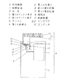
図1は本発明の一実施の形態のアンテナが搭載された無線装置を模式的に表した図であり、同図に示すように、地板8に対し並べて配置されているアンテナ13は、第1の周波数に共振する第1のアンテナ素子11と第2の周波数に共振する第2のアンテナ素子12とを備えている。
(Embodiment)
FIG. 1 is a diagram schematically showing a radio apparatus equipped with an antenna according to an embodiment of the present invention. As shown in FIG. 1, the
そして、第1のアンテナ素子11は、地板8上に配置された第1の給電点14に接続され、その第1の給電点14に第1の整合回路16の一端が接続され、前記第1の整合回路16の他端は、接続点18に接続されている。
The
また、第2のアンテナ素子12は、地板8上に配置された第2の給電点15に接続され、その第2の給電点15に第2の整合回路17の一端が接続され、前記第2の整合回路17の他端は、前記第1のアンテナ素子11の場合と同じく接続点18に接続されている。
The
そして、前記接続点18は、伝送線路6を介して無線回路7へと接続され、それらで無線装置19が構成されている。
The
ここで、第1のアンテナ素子11はGSM(880〜960MHz)に共振し、第2のアンテナ素子12はDCS(1710〜1880MHz)に共振しており、第2のアンテナ素子12は第1のアンテナ素子11より高い周波数で共振しているものとする。
Here, the
そして、前記第1の整合回路16は、第1の給電点14と接続点18に対し直列に接続されたインダクタ20で構成されている。また、前記第2の整合回路17は、第2の給電点15と接続点18に対し直列に接続されたコンデンサ22と、地板8と第2の給電点15に対し直列に接続されたインダクタ21とで構成されている。
The first matching circuit 16 includes an inductor 20 connected in series to the
以上の構成において、第1のアンテナ素子11がGSMに共振し、また第2のアンテナ素子12がDCSに共振して、従来の技術で説明した原理と同様に、各々の電波が送受信できる。その結果、無線装置19は、GSMとDCSの2つの周波数に対応したアンテナが搭載されたものとなっている。
In the above configuration, the
このように本実施の形態によれば、第1のアンテナ素子11と第2のアンテナ素子12にそれぞれ独立した給電点14と15を設けてあることにより、2つのアンテナ素子11と12間の結合ロスを低減させることができる。また、それに加えて、アンテナ素子11と12毎にそれぞれ独立した整合回路16と17を設けてあるため、任意に独立して2つの異なる周波数の調整が容易に可能となる。
As described above, according to the present embodiment, the
そして、整合回路16と17を前記構成のものとすると、第1の周波数では、第2の整合回路17のコンデンサ22により、第2のアンテナ素子12と伝送線路6とが電気的に分断されると共に、第2の整合回路17のインダクタ21により第2のアンテナ素子12が地板8と電気的に接続され、第2のアンテナ素子12が無給電素子として機能するようにできる。この結果、第1のアンテナ素子11と無給電素子として機能する第2のアンテナ素子12との複共振により、第1の周波数が広帯域なものにできる。
When the matching
ここで、第1の整合回路16のインダクタ20は、第1の周波数では、第1のアンテナ素子11の共振周波数を低くするように作用するため第1のアンテナ素子11の小形化も図れる。また、第1の周波数より高い第2の周波数では、インダクタ20により第1のアンテナ素子11と伝送線路6とを電気的に遮断する効果もあるため、2つの周波数を独立して調整することがさらに容易に行えるようにできるという効果が得られる。
Here, since the inductor 20 of the first matching circuit 16 acts to lower the resonance frequency of the
なお、整合回路の受動素子の配列は、図1に示す配列に限ったものではなく、インダクタやコンデンサの受動素子を自由に任意の場所に配列してインピーダンスを自由に調整してもよい。なお、このときにも前述した思想が充足できる構成とする方が好ましい。 The arrangement of the passive elements of the matching circuit is not limited to the arrangement shown in FIG. 1, and the impedance may be freely adjusted by freely arranging the passive elements of the inductor and the capacitor at arbitrary positions. In this case, it is preferable that the above-described idea can be satisfied.
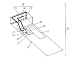
なお、図1には第1のアンテナ素子11をメアンダで構成したものを図示しているが、この構成に限ったものではない。具体的な例として、図2に示すように、第1のアンテナ素子23として、折り返しモノポールで構成してもよい。また、螺旋状、板状、もしくは、それらの組み合わせ等で構成してもよい。同様に、第2のアンテナ素子12についても様々なもので構成してもよい。さらに、第1のアンテナ素子11の一部もしくは第2のアンテナ素子12の一部を地板8に接地させ、逆Fアンテナとして機能させてもよく、その構成であればインピーダンス調整の自由度がさらに高まる。
Although FIG. 1 shows the
そして、前述の図2に示すように、第1のアンテナ素子23と第2のアンテナ素子24とが絶縁樹脂25により一体成形されてアンテナ26に構成されたものであれば、絶縁樹脂25によりアンテナ素子23、24の変形が抑えられると共に、絶縁樹脂25の誘電率によりアンテナ26自体の小形化も容易である。
As shown in FIG. 2, if the
さらに、同図に示すように、第1のアンテナ素子23および第2のアンテナ素子24を、りん青銅などのばね性を有する金属材料で構成し、その各端部を、地板8に配された第1の給電点27および第2の給電点28にそれぞれ圧接接続させるものとすると、アンテナ26と各給電点27、28とを半田を用いないで簡易に接続できる。なお、当該構成部分を備えた無線装置31も、前述したものと同じく、第1および第2の給電点27および28に、各々、第1および第2の整合回路29および30の一端が接続され、その整合回路29および30の他端は、それぞれ接続点18に接続され、接続点18は伝送線路6を介して無線回路7に接続されているため、アンテナ素子23および24に応じた個々の共振周波数に対して独立して容易に調整可能なものにできる。
Further, as shown in the figure, the
本発明によるアンテナが搭載された無線装置は、2つのアンテナ素子間の結合ロスを低減させることができ、多周波で任意に独立して異なる共振周波数への調整が容易に行える、アンテナが搭載された無線装置が実現できるという効果を有し、携帯電話などの移動体通信等に有用である。 A radio apparatus equipped with an antenna according to the present invention can reduce the coupling loss between two antenna elements, and can be easily adjusted to different resonance frequencies arbitrarily and independently at multiple frequencies. This is advantageous in that a wireless device can be realized, and is useful for mobile communication such as a mobile phone.
6 伝送線路
7 無線回路
8 地板
11、23 第1のアンテナ素子
12、24 第2のアンテナ素子
13、26 アンテナ
14、27 第1の給電点
15、28 第2の給電点
16、29 第1の整合回路
17、30 第2の整合回路
18 接続点
19、31 無線装置
20、21 インダクタ
22 コンデンサ
25 絶縁樹脂
6
Claims (5)
Priority Applications (5)
| Application Number | Priority Date | Filing Date | Title |
|---|---|---|---|
| JP2004051083A JP4301034B2 (en) | 2004-02-26 | 2004-02-26 | Wireless device with antenna |
| US11/023,494 US7084831B2 (en) | 2004-02-26 | 2004-12-29 | Wireless device having antenna |
| EP05000402A EP1569300B1 (en) | 2004-02-26 | 2005-01-11 | Wireless device having antenna |
| DE602005014824T DE602005014824D1 (en) | 2004-02-26 | 2005-01-11 | Wireless device with antenna |
| CN2005100044087A CN1661855A (en) | 2004-02-26 | 2005-01-13 | wireless device with antenna |
Applications Claiming Priority (1)
| Application Number | Priority Date | Filing Date | Title |
|---|---|---|---|
| JP2004051083A JP4301034B2 (en) | 2004-02-26 | 2004-02-26 | Wireless device with antenna |
Publications (2)
| Publication Number | Publication Date |
|---|---|
| JP2005244553A JP2005244553A (en) | 2005-09-08 |
| JP4301034B2 true JP4301034B2 (en) | 2009-07-22 |
Family
ID=34747494
Family Applications (1)
| Application Number | Title | Priority Date | Filing Date |
|---|---|---|---|
| JP2004051083A Expired - Fee Related JP4301034B2 (en) | 2004-02-26 | 2004-02-26 | Wireless device with antenna |
Country Status (5)
| Country | Link |
|---|---|
| US (1) | US7084831B2 (en) |
| EP (1) | EP1569300B1 (en) |
| JP (1) | JP4301034B2 (en) |
| CN (1) | CN1661855A (en) |
| DE (1) | DE602005014824D1 (en) |
Families Citing this family (102)
| Publication number | Priority date | Publication date | Assignee | Title |
|---|---|---|---|---|
| FI116332B (en) * | 2002-12-16 | 2005-10-31 | Lk Products Oy | Antenna for a flat radio |
| EP1864352A1 (en) * | 2005-03-30 | 2007-12-12 | Nokia Corporation | An antenna |
| US7495620B2 (en) * | 2005-04-07 | 2009-02-24 | Nokia Corporation | Antenna |
| FI20055420A0 (en) | 2005-07-25 | 2005-07-25 | Lk Products Oy | Adjustable multi-band antenna |
| TWI313082B (en) * | 2005-08-16 | 2009-08-01 | Wistron Neweb Corp | Notebook and antenna thereof |
| WO2007029741A1 (en) * | 2005-09-09 | 2007-03-15 | Matsushita Electric Industrial Co., Ltd. | Wireless unit antenna apparatus and mobile wireless unit |
| US7605763B2 (en) * | 2005-09-15 | 2009-10-20 | Dell Products L.P. | Combination antenna with multiple feed points |
| FI119009B (en) | 2005-10-03 | 2008-06-13 | Pulse Finland Oy | Multiple-band antenna |
| FI118782B (en) | 2005-10-14 | 2008-03-14 | Pulse Finland Oy | Adjustable antenna |
| JP4868128B2 (en) * | 2006-04-10 | 2012-02-01 | 日立金属株式会社 | ANTENNA DEVICE AND RADIO COMMUNICATION DEVICE USING THE SAME |
| FR2901063A1 (en) * | 2006-05-12 | 2007-11-16 | Thomson Licensing Sas | PORTABLE COMPACT ANTENNA FOR DIGITAL TERRESTRIAL TELEVISION |
| US9007275B2 (en) | 2006-06-08 | 2015-04-14 | Fractus, S.A. | Distributed antenna system robust to human body loading effects |
| JP4957724B2 (en) * | 2006-07-11 | 2012-06-20 | 株式会社村田製作所 | Antenna and wireless IC device |
| US8618990B2 (en) | 2011-04-13 | 2013-12-31 | Pulse Finland Oy | Wideband antenna and methods |
| US8738103B2 (en) | 2006-07-18 | 2014-05-27 | Fractus, S.A. | Multiple-body-configuration multimedia and smartphone multifunction wireless devices |
| EP1892798A1 (en) * | 2006-08-22 | 2008-02-27 | Matsushita Electric Industrial Co., Ltd. | Folded planar monopole antenna |
| WO2008045151A1 (en) * | 2006-10-05 | 2008-04-17 | Pulse Finland Oy | Multi-band antenna with a common resonant feed structure and methods |
| EP2092641B1 (en) * | 2006-11-17 | 2016-10-05 | Nokia Technologies Oy | An apparatus for enabling two elements to share a common feed |
| US7782261B2 (en) * | 2006-12-20 | 2010-08-24 | Nokia Corporation | Antenna arrangement |
| JP2008167098A (en) | 2006-12-28 | 2008-07-17 | Nec Saitama Ltd | Antenna system and portable radio equipment using the antenna system |
| FI120119B (en) * | 2007-01-04 | 2009-06-30 | Pulse Finland Oy | The antenna structure |
| JP4571988B2 (en) * | 2007-01-19 | 2010-10-27 | パナソニック株式会社 | Array antenna device and wireless communication device |
| KR100848038B1 (en) * | 2007-02-14 | 2008-07-23 | 주식회사 이엠따블유안테나 | Multiband antenna |
| US8611958B2 (en) * | 2007-03-29 | 2013-12-17 | Kyocera Corporation | Portable wireless device |
| WO2008119699A1 (en) * | 2007-03-30 | 2008-10-09 | Fractus, S.A. | Wireless device including a multiband antenna system |
| US7639188B2 (en) * | 2007-04-05 | 2009-12-29 | Sony Ericsson Mobile Communications Ab | Radio antenna for a communication terminal |
| WO2008126724A1 (en) | 2007-04-05 | 2008-10-23 | Murata Manufacturing Co., Ltd. | Antenna and radio communication device |
| FI20075269A0 (en) | 2007-04-19 | 2007-04-19 | Pulse Finland Oy | Method and arrangement for antenna matching |
| EP2143167A4 (en) * | 2007-05-02 | 2013-05-15 | Nokia Corp | An antenna arrangement |
| TWI414109B (en) * | 2007-05-02 | 2013-11-01 | Lite On Technology Corp | Two - branch broadband antenna and digital tv device having the same |
| JP2008288871A (en) * | 2007-05-17 | 2008-11-27 | Nec Corp | Dual band antenna and communication terminal |
| KR101383465B1 (en) * | 2007-06-11 | 2014-04-10 | 삼성전자주식회사 | Apparatus for multiband antenna in mobile phone |
| US7701401B2 (en) * | 2007-07-04 | 2010-04-20 | Kabushiki Kaisha Toshiba | Antenna device having no less than two antenna elements |
| US7710332B2 (en) * | 2007-08-17 | 2010-05-04 | Htc Corporation | Mobile communications device with a compact-sized three-dimensional antenna |
| US7859468B2 (en) * | 2007-08-30 | 2010-12-28 | Research In Motion Limited | Mobile wireless communications device including a folded monopole multi-band antenna and related methods |
| FI120427B (en) | 2007-08-30 | 2009-10-15 | Pulse Finland Oy | Adjustable multiband antenna |
| JP5062888B2 (en) * | 2008-01-09 | 2012-10-31 | パナソニック株式会社 | Wireless communication terminal |
| US7825860B2 (en) * | 2008-04-16 | 2010-11-02 | Sony Ericsson Mobile Communications Ab | Antenna assembly |
| US7768463B2 (en) | 2008-04-16 | 2010-08-03 | Sony Ericsson Mobile Communications Ab | Antenna assembly, printed wiring board and device |
| JP5093348B2 (en) * | 2008-06-06 | 2012-12-12 | 株式会社村田製作所 | Multiband antenna and its mounting structure |
| JP5009240B2 (en) * | 2008-06-25 | 2012-08-22 | ソニーモバイルコミュニケーションズ株式会社 | Multiband antenna and wireless communication terminal |
| US7834814B2 (en) * | 2008-06-25 | 2010-11-16 | Nokia Corporation | Antenna arrangement |
| JP4784636B2 (en) | 2008-10-28 | 2011-10-05 | Tdk株式会社 | Surface mount antenna, antenna device using the same, and radio communication device |
| JP5440603B2 (en) * | 2009-04-24 | 2014-03-12 | 株式会社村田製作所 | Antenna and wireless communication device |
| GB0907361D0 (en) * | 2009-04-29 | 2009-06-10 | Lok8U Ltd | A tracking and communications device |
| FI20096134A0 (en) | 2009-11-03 | 2009-11-03 | Pulse Finland Oy | Adjustable antenna |
| WO2011055159A1 (en) * | 2009-11-04 | 2011-05-12 | Laird Technologies Ab | Multi-frequency antenna assemblies with multiple antennas |
| US8514132B2 (en) * | 2009-11-10 | 2013-08-20 | Research In Motion Limited | Compact multiple-band antenna for wireless devices |
| FI20096251A0 (en) | 2009-11-27 | 2009-11-27 | Pulse Finland Oy | MIMO antenna |
| EP2333901A3 (en) * | 2009-12-11 | 2011-07-13 | Samsung Electronics Co., Ltd. | Antenna device |
| FI20096320A0 (en) * | 2009-12-14 | 2009-12-14 | Pulse Finland Oy | Multiband antenna structure |
| EP2337150B1 (en) * | 2009-12-18 | 2012-12-05 | Laird Technologies AB | An antenna arrangement and a portable radio communication device comprising such an antenna arrangement |
| US8604980B2 (en) | 2009-12-22 | 2013-12-10 | Motorola Mobility Llc | Antenna system with non-resonating structure |
| US8847833B2 (en) | 2009-12-29 | 2014-09-30 | Pulse Finland Oy | Loop resonator apparatus and methods for enhanced field control |
| FI20105158A7 (en) | 2010-02-18 | 2011-08-19 | Pulse Finland Oy | ANTENNA EQUIPPED WITH SHELL RADIATOR |
| US9406998B2 (en) | 2010-04-21 | 2016-08-02 | Pulse Finland Oy | Distributed multiband antenna and methods |
| JP5234084B2 (en) | 2010-11-05 | 2013-07-10 | 株式会社村田製作所 | Antenna device and communication terminal device |
| FI20115072A0 (en) | 2011-01-25 | 2011-01-25 | Pulse Finland Oy | Multi-resonance antenna, antenna module and radio unit |
| US9673507B2 (en) | 2011-02-11 | 2017-06-06 | Pulse Finland Oy | Chassis-excited antenna apparatus and methods |
| US8648752B2 (en) | 2011-02-11 | 2014-02-11 | Pulse Finland Oy | Chassis-excited antenna apparatus and methods |
| JP5505561B2 (en) * | 2011-05-09 | 2014-05-28 | 株式会社村田製作所 | Coupling degree adjusting circuit, antenna device, and communication terminal device |
| JP2012248947A (en) * | 2011-05-25 | 2012-12-13 | Panasonic Corp | Portable wireless device |
| US8866689B2 (en) | 2011-07-07 | 2014-10-21 | Pulse Finland Oy | Multi-band antenna and methods for long term evolution wireless system |
| US9450291B2 (en) | 2011-07-25 | 2016-09-20 | Pulse Finland Oy | Multiband slot loop antenna apparatus and methods |
| US8639194B2 (en) * | 2011-09-28 | 2014-01-28 | Motorola Mobility Llc | Tunable antenna with a conductive, physical component co-located with the antenna |
| US9123990B2 (en) | 2011-10-07 | 2015-09-01 | Pulse Finland Oy | Multi-feed antenna apparatus and methods |
| US9531058B2 (en) | 2011-12-20 | 2016-12-27 | Pulse Finland Oy | Loosely-coupled radio antenna apparatus and methods |
| US9484619B2 (en) | 2011-12-21 | 2016-11-01 | Pulse Finland Oy | Switchable diversity antenna apparatus and methods |
| MY160952A (en) * | 2012-02-15 | 2017-03-31 | Motorola Solutions Inc | Hybrid antenna for portable communication devices |
| WO2013127128A1 (en) * | 2012-03-01 | 2013-09-06 | 深圳光启高等理工研究院 | Antenna device |
| KR101887934B1 (en) * | 2012-03-26 | 2018-09-06 | 삼성전자주식회사 | Built-in antenna for communication electronic device |
| US8988296B2 (en) | 2012-04-04 | 2015-03-24 | Pulse Finland Oy | Compact polarized antenna and methods |
| TWI504057B (en) * | 2012-05-23 | 2015-10-11 | Cho Yi Lin | Portable communication apparatus |
| US10096910B2 (en) * | 2012-06-13 | 2018-10-09 | Skycross Co., Ltd. | Multimode antenna structures and methods thereof |
| US9331389B2 (en) | 2012-07-16 | 2016-05-03 | Fractus Antennas, S.L. | Wireless handheld devices, radiation systems and manufacturing methods |
| US9979078B2 (en) | 2012-10-25 | 2018-05-22 | Pulse Finland Oy | Modular cell antenna apparatus and methods |
| US10069209B2 (en) | 2012-11-06 | 2018-09-04 | Pulse Finland Oy | Capacitively coupled antenna apparatus and methods |
| US9647338B2 (en) | 2013-03-11 | 2017-05-09 | Pulse Finland Oy | Coupled antenna structure and methods |
| US10079428B2 (en) | 2013-03-11 | 2018-09-18 | Pulse Finland Oy | Coupled antenna structure and methods |
| US9893427B2 (en) * | 2013-03-14 | 2018-02-13 | Ethertronics, Inc. | Antenna-like matching component |
| CN103268987B (en) * | 2013-05-10 | 2015-07-29 | 上海安费诺永亿通讯电子有限公司 | A kind of small size three is unification multifrequency ceramic antenna frequently |
| TWI539661B (en) | 2013-06-26 | 2016-06-21 | 宏碁股份有限公司 | Communication device |
| US9634383B2 (en) | 2013-06-26 | 2017-04-25 | Pulse Finland Oy | Galvanically separated non-interacting antenna sector apparatus and methods |
| CN104283005A (en) * | 2013-07-09 | 2015-01-14 | 宏碁股份有限公司 | communication device |
| TWM470398U (en) * | 2013-07-19 | 2014-01-11 | Chi Mei Comm Systems Inc | Antenna device |
| US9680212B2 (en) | 2013-11-20 | 2017-06-13 | Pulse Finland Oy | Capacitive grounding methods and apparatus for mobile devices |
| US9590308B2 (en) | 2013-12-03 | 2017-03-07 | Pulse Electronics, Inc. | Reduced surface area antenna apparatus and mobile communications devices incorporating the same |
| WO2015100642A1 (en) * | 2013-12-31 | 2015-07-09 | 华为终端有限公司 | Matching circuit of antenna |
| US9350081B2 (en) | 2014-01-14 | 2016-05-24 | Pulse Finland Oy | Switchable multi-radiator high band antenna apparatus |
| CN110380192A (en) | 2014-07-24 | 2019-10-25 | 弗拉克托斯天线股份有限公司 | The ultra-thin radiating system of electronic equipment |
| US9948002B2 (en) | 2014-08-26 | 2018-04-17 | Pulse Finland Oy | Antenna apparatus with an integrated proximity sensor and methods |
| US9973228B2 (en) | 2014-08-26 | 2018-05-15 | Pulse Finland Oy | Antenna apparatus with an integrated proximity sensor and methods |
| US9722308B2 (en) | 2014-08-28 | 2017-08-01 | Pulse Finland Oy | Low passive intermodulation distributed antenna system for multiple-input multiple-output systems and methods of use |
| CN104269606B (en) * | 2014-10-24 | 2018-05-01 | 广东欧珀移动通信有限公司 | A kind of mobile terminal antenna structure and mobile terminal |
| EP3295518B1 (en) * | 2015-05-11 | 2021-09-29 | Carrier Corporation | Antenna with reversing current elements |
| US10305169B2 (en) | 2015-05-18 | 2019-05-28 | Huawei Technologies Co., Ltd. | Antenna apparatus and terminal |
| US9906260B2 (en) | 2015-07-30 | 2018-02-27 | Pulse Finland Oy | Sensor-based closed loop antenna swapping apparatus and methods |
| JP6451865B2 (en) * | 2015-10-14 | 2019-01-16 | 株式会社村田製作所 | Antenna device |
| SG10201609104UA (en) | 2016-10-31 | 2018-05-30 | Delta Electronics Inc | Dual-band dual-port antenna structure |
| WO2019208253A1 (en) * | 2018-04-25 | 2019-10-31 | 株式会社村田製作所 | Antenna device and communication terminal apparatus |
| JP6760545B2 (en) * | 2018-04-25 | 2020-09-23 | 株式会社村田製作所 | Antenna coupling element, antenna device and communication terminal device |
| CN117810690B (en) * | 2022-09-23 | 2025-10-31 | 华为终端有限公司 | Antenna structure and electronic equipment |
Family Cites Families (14)
| Publication number | Priority date | Publication date | Assignee | Title |
|---|---|---|---|---|
| JPS62188507A (en) * | 1986-02-14 | 1987-08-18 | Mitsubishi Electric Corp | Antenna system |
| JPH1188246A (en) * | 1997-09-08 | 1999-03-30 | Matsushita Electric Ind Co Ltd | Antenna device and wireless receiving device using the same |
| JPH11122033A (en) * | 1997-10-09 | 1999-04-30 | Tdk Corp | Antenna system |
| JPH11177327A (en) * | 1997-12-09 | 1999-07-02 | Nec Saitama Ltd | Inverse f antenna device |
| JP2000183644A (en) * | 1998-12-17 | 2000-06-30 | Matsushita Electric Ind Co Ltd | Antenna device |
| US6198442B1 (en) | 1999-07-22 | 2001-03-06 | Ericsson Inc. | Multiple frequency band branch antennas for wireless communicators |
| JP2003152428A (en) * | 2000-12-27 | 2003-05-23 | Furukawa Electric Co Ltd:The | Small antenna and manufacturing method thereof |
| JP3678167B2 (en) | 2001-05-02 | 2005-08-03 | 株式会社村田製作所 | ANTENNA DEVICE AND RADIO COMMUNICATION DEVICE HAVING THE ANTENNA DEVICE |
| EP1289061A3 (en) | 2001-08-24 | 2004-10-06 | Hirschmann Electronics GmbH & Co. KG | Antenna system |
| JP2003101335A (en) * | 2001-09-25 | 2003-04-04 | Matsushita Electric Ind Co Ltd | Antenna device and communication device using the same |
| US6618014B2 (en) | 2001-09-28 | 2003-09-09 | Centurion Wireless Tech., Inc. | Integral antenna and radio system |
| JP2003249811A (en) * | 2001-12-20 | 2003-09-05 | Murata Mfg Co Ltd | Double-resonance antenna apparatus |
| US7184727B2 (en) * | 2002-02-12 | 2007-02-27 | Kyocera Wireless Corp. | Full-duplex antenna system and method |
| US6914570B2 (en) * | 2003-11-10 | 2005-07-05 | Motorola, Inc. | Antenna system for a communication device |
-
2004
- 2004-02-26 JP JP2004051083A patent/JP4301034B2/en not_active Expired - Fee Related
- 2004-12-29 US US11/023,494 patent/US7084831B2/en not_active Expired - Fee Related
-
2005
- 2005-01-11 EP EP05000402A patent/EP1569300B1/en not_active Expired - Fee Related
- 2005-01-11 DE DE602005014824T patent/DE602005014824D1/en not_active Expired - Lifetime
- 2005-01-13 CN CN2005100044087A patent/CN1661855A/en active Pending
Also Published As
| Publication number | Publication date |
|---|---|
| CN1661855A (en) | 2005-08-31 |
| DE602005014824D1 (en) | 2009-07-23 |
| US7084831B2 (en) | 2006-08-01 |
| JP2005244553A (en) | 2005-09-08 |
| US20050190107A1 (en) | 2005-09-01 |
| EP1569300B1 (en) | 2009-06-10 |
| EP1569300A1 (en) | 2005-08-31 |
Similar Documents
| Publication | Publication Date | Title |
|---|---|---|
| JP4301034B2 (en) | Wireless device with antenna | |
| US6204826B1 (en) | Flat dual frequency band antennas for wireless communicators | |
| US6662028B1 (en) | Multiple frequency inverted-F antennas having multiple switchable feed points and wireless communicators incorporating the same | |
| JP4523211B2 (en) | Folding dual frequency band antenna for wireless communication device | |
| JP4297012B2 (en) | antenna | |
| US6218992B1 (en) | Compact, broadband inverted-F antennas with conductive elements and wireless communicators incorporating same | |
| EP1992042B1 (en) | Multi-frequency band antenna device for radio communication terminal | |
| JP4003077B2 (en) | Antenna and wireless communication device | |
| US6417816B2 (en) | Dual band bowtie/meander antenna | |
| US6204819B1 (en) | Convertible loop/inverted-f antennas and wireless communicators incorporating the same | |
| US8599074B2 (en) | Mobile communication device and antenna thereof | |
| US6229487B1 (en) | Inverted-F antennas having non-linear conductive elements and wireless communicators incorporating the same | |
| CN102099962B (en) | Antenna arrangement | |
| US6184836B1 (en) | Dual band antenna having mirror image meandering segments and wireless communicators incorporating same | |
| JPWO2004109857A1 (en) | Antenna and electronic equipment using it | |
| US9660347B2 (en) | Printed coupled-fed multi-band antenna and electronic system | |
| CN102683861A (en) | Tunable loop antennas | |
| US6563466B2 (en) | Multi-frequency band inverted-F antennas with coupled branches and wireless communicators incorporating same | |
| KR20110122849A (en) | Antenna devices, printed circuit boards, portable electronic devices and conversion kits | |
| US6697023B1 (en) | Built-in multi-band mobile phone antenna with meandering conductive portions | |
| JP2007159140A (en) | Sliding mobile communication terminal antenna | |
| US9548538B2 (en) | Antenna arrangement and device | |
| KR20000017083A (en) | Antenna Device | |
| CN100444464C (en) | Antennas and electronic devices using antennas | |
| JP2006067234A (en) | Antenna device |
Legal Events
| Date | Code | Title | Description |
|---|---|---|---|
| A621 | Written request for application examination |
Free format text: JAPANESE INTERMEDIATE CODE: A621 Effective date: 20061101 |
|
| RD01 | Notification of change of attorney |
Free format text: JAPANESE INTERMEDIATE CODE: A7421 Effective date: 20061213 |
|
| A977 | Report on retrieval |
Free format text: JAPANESE INTERMEDIATE CODE: A971007 Effective date: 20080404 |
|
| A131 | Notification of reasons for refusal |
Free format text: JAPANESE INTERMEDIATE CODE: A131 Effective date: 20080408 |
|
| A521 | Request for written amendment filed |
Free format text: JAPANESE INTERMEDIATE CODE: A523 Effective date: 20080609 |
|
| A131 | Notification of reasons for refusal |
Free format text: JAPANESE INTERMEDIATE CODE: A131 Effective date: 20080930 |
|
| A521 | Request for written amendment filed |
Free format text: JAPANESE INTERMEDIATE CODE: A523 Effective date: 20081031 |
|
| TRDD | Decision of grant or rejection written | ||
| A01 | Written decision to grant a patent or to grant a registration (utility model) |
Free format text: JAPANESE INTERMEDIATE CODE: A01 Effective date: 20090331 |
|
| A01 | Written decision to grant a patent or to grant a registration (utility model) |
Free format text: JAPANESE INTERMEDIATE CODE: A01 |
|
| FPAY | Renewal fee payment (event date is renewal date of database) |
Free format text: PAYMENT UNTIL: 20120501 Year of fee payment: 3 |
|
| A61 | First payment of annual fees (during grant procedure) |
Free format text: JAPANESE INTERMEDIATE CODE: A61 Effective date: 20090413 |
|
| FPAY | Renewal fee payment (event date is renewal date of database) |
Free format text: PAYMENT UNTIL: 20120501 Year of fee payment: 3 |
|
| FPAY | Renewal fee payment (event date is renewal date of database) |
Free format text: PAYMENT UNTIL: 20120501 Year of fee payment: 3 |
|
| FPAY | Renewal fee payment (event date is renewal date of database) |
Free format text: PAYMENT UNTIL: 20130501 Year of fee payment: 4 |
|
| LAPS | Cancellation because of no payment of annual fees |