WO2020262472A1 - 電子部品収納用パッケージ、電子装置、および電子モジュール - Google Patents
電子部品収納用パッケージ、電子装置、および電子モジュール Download PDFInfo
- Publication number
- WO2020262472A1 WO2020262472A1 PCT/JP2020/024858 JP2020024858W WO2020262472A1 WO 2020262472 A1 WO2020262472 A1 WO 2020262472A1 JP 2020024858 W JP2020024858 W JP 2020024858W WO 2020262472 A1 WO2020262472 A1 WO 2020262472A1
- Authority
- WO
- WIPO (PCT)
- Prior art keywords
- conductor
- insulating substrate
- inner layer
- electronic component
- external connecting
- Prior art date
- Legal status (The legal status is an assumption and is not a legal conclusion. Google has not performed a legal analysis and makes no representation as to the accuracy of the status listed.)
- Ceased
Links
Images



Classifications
-
- H—ELECTRICITY
- H03—ELECTRONIC CIRCUITRY
- H03H—IMPEDANCE NETWORKS, e.g. RESONANT CIRCUITS; RESONATORS
- H03H9/00—Networks comprising electromechanical or electro-acoustic elements; Electromechanical resonators
- H03H9/02—Details
-
- H—ELECTRICITY
- H03—ELECTRONIC CIRCUITRY
- H03H—IMPEDANCE NETWORKS, e.g. RESONANT CIRCUITS; RESONATORS
- H03H9/00—Networks comprising electromechanical or electro-acoustic elements; Electromechanical resonators
- H03H9/02—Details
- H03H9/05—Holders or supports
- H03H9/0504—Holders or supports for bulk acoustic wave devices
- H03H9/0514—Holders or supports for bulk acoustic wave devices consisting of mounting pads or bumps
- H03H9/0523—Holders or supports for bulk acoustic wave devices consisting of mounting pads or bumps for flip-chip mounting
-
- H—ELECTRICITY
- H10—SEMICONDUCTOR DEVICES; ELECTRIC SOLID-STATE DEVICES NOT OTHERWISE PROVIDED FOR
- H10W—GENERIC PACKAGES, INTERCONNECTIONS, CONNECTORS OR OTHER CONSTRUCTIONAL DETAILS OF DEVICES COVERED BY CLASS H10
- H10W70/00—Package substrates; Interposers; Redistribution layers [RDL]
- H10W70/60—Insulating or insulated package substrates; Interposers; Redistribution layers
- H10W70/67—Insulating or insulated package substrates; Interposers; Redistribution layers characterised by their insulating layers or insulating parts
- H10W70/68—Shapes or dispositions thereof
-
- H—ELECTRICITY
- H03—ELECTRONIC CIRCUITRY
- H03H—IMPEDANCE NETWORKS, e.g. RESONANT CIRCUITS; RESONATORS
- H03H9/00—Networks comprising electromechanical or electro-acoustic elements; Electromechanical resonators
- H03H9/02—Details
- H03H9/05—Holders or supports
- H03H9/0504—Holders or supports for bulk acoustic wave devices
- H03H9/0514—Holders or supports for bulk acoustic wave devices consisting of mounting pads or bumps
-
- H—ELECTRICITY
- H03—ELECTRONIC CIRCUITRY
- H03H—IMPEDANCE NETWORKS, e.g. RESONANT CIRCUITS; RESONATORS
- H03H9/00—Networks comprising electromechanical or electro-acoustic elements; Electromechanical resonators
- H03H9/02—Details
- H03H9/05—Holders or supports
- H03H9/10—Mounting in enclosures
- H03H9/1007—Mounting in enclosures for bulk acoustic wave [BAW] devices
- H03H9/1014—Mounting in enclosures for bulk acoustic wave [BAW] devices the enclosure being defined by a frame built on a substrate and a cap, the frame having no mechanical contact with the BAW device
- H03H9/1021—Mounting in enclosures for bulk acoustic wave [BAW] devices the enclosure being defined by a frame built on a substrate and a cap, the frame having no mechanical contact with the BAW device the BAW device being of the cantilever type
-
- H—ELECTRICITY
- H03—ELECTRONIC CIRCUITRY
- H03H—IMPEDANCE NETWORKS, e.g. RESONANT CIRCUITS; RESONATORS
- H03H9/00—Networks comprising electromechanical or electro-acoustic elements; Electromechanical resonators
- H03H9/15—Constructional features of resonators consisting of piezoelectric or electrostrictive material
- H03H9/17—Constructional features of resonators consisting of piezoelectric or electrostrictive material having a single resonator
- H03H9/19—Constructional features of resonators consisting of piezoelectric or electrostrictive material having a single resonator consisting of quartz
-
- H—ELECTRICITY
- H10—SEMICONDUCTOR DEVICES; ELECTRIC SOLID-STATE DEVICES NOT OTHERWISE PROVIDED FOR
- H10W—GENERIC PACKAGES, INTERCONNECTIONS, CONNECTORS OR OTHER CONSTRUCTIONAL DETAILS OF DEVICES COVERED BY CLASS H10
- H10W70/00—Package substrates; Interposers; Redistribution layers [RDL]
- H10W70/60—Insulating or insulated package substrates; Interposers; Redistribution layers
-
- H—ELECTRICITY
- H10—SEMICONDUCTOR DEVICES; ELECTRIC SOLID-STATE DEVICES NOT OTHERWISE PROVIDED FOR
- H10W—GENERIC PACKAGES, INTERCONNECTIONS, CONNECTORS OR OTHER CONSTRUCTIONAL DETAILS OF DEVICES COVERED BY CLASS H10
- H10W70/00—Package substrates; Interposers; Redistribution layers [RDL]
- H10W70/60—Insulating or insulated package substrates; Interposers; Redistribution layers
- H10W70/62—Insulating or insulated package substrates; Interposers; Redistribution layers characterised by their interconnections
- H10W70/65—Shapes or dispositions of interconnections
- H10W70/657—Shapes or dispositions of interconnections on sidewalls or bottom surfaces of the package substrates, interposers or redistribution layers
-
- H—ELECTRICITY
- H10—SEMICONDUCTOR DEVICES; ELECTRIC SOLID-STATE DEVICES NOT OTHERWISE PROVIDED FOR
- H10W—GENERIC PACKAGES, INTERCONNECTIONS, CONNECTORS OR OTHER CONSTRUCTIONAL DETAILS OF DEVICES COVERED BY CLASS H10
- H10W76/00—Containers; Fillings or auxiliary members therefor; Seals
- H10W76/10—Containers or parts thereof
- H10W76/12—Containers or parts thereof characterised by their shape
-
- H—ELECTRICITY
- H10—SEMICONDUCTOR DEVICES; ELECTRIC SOLID-STATE DEVICES NOT OTHERWISE PROVIDED FOR
- H10W—GENERIC PACKAGES, INTERCONNECTIONS, CONNECTORS OR OTHER CONSTRUCTIONAL DETAILS OF DEVICES COVERED BY CLASS H10
- H10W76/00—Containers; Fillings or auxiliary members therefor; Seals
- H10W76/10—Containers or parts thereof
- H10W76/12—Containers or parts thereof characterised by their shape
- H10W76/15—Containers comprising an insulating or insulated base
- H10W76/153—Containers comprising an insulating or insulated base having interconnections in passages through the insulating or insulated base
-
- H—ELECTRICITY
- H10—SEMICONDUCTOR DEVICES; ELECTRIC SOLID-STATE DEVICES NOT OTHERWISE PROVIDED FOR
- H10W—GENERIC PACKAGES, INTERCONNECTIONS, CONNECTORS OR OTHER CONSTRUCTIONAL DETAILS OF DEVICES COVERED BY CLASS H10
- H10W99/00—Subject matter not provided for in other groups of this subclass
-
- H—ELECTRICITY
- H10—SEMICONDUCTOR DEVICES; ELECTRIC SOLID-STATE DEVICES NOT OTHERWISE PROVIDED FOR
- H10W—GENERIC PACKAGES, INTERCONNECTIONS, CONNECTORS OR OTHER CONSTRUCTIONAL DETAILS OF DEVICES COVERED BY CLASS H10
- H10W74/00—Encapsulations, e.g. protective coatings
- H10W74/01—Manufacture or treatment
- H10W74/014—Manufacture or treatment using batch processing
Definitions
- the present invention relates to a package for storing electronic components, an electronic device, and an electronic module for accommodating electronic components such as piezoelectric vibrating elements or semiconductor elements.
- a package for storing electronic components has been devised in which electronic components are housed in a concave mounting portion and the electronic components of the mounting portion are connected to a wiring conductor provided outside.
- the mounting portion is hermetically sealed with a lid to form an electronic device, which facilitates its handling and wiring connection (see, for example, Japanese Patent Application Laid-Open No. 2002-164451). .).
- the electronic component storage package of the present disclosure includes an insulating substrate having a main surface, an external connecting conductor whose main surface is partially exposed, and an inner layer located inside the insulating substrate in the thickness direction of the external connecting conductor.
- the external connecting conductor has a protrusion toward the inner layer conductor, and the protrusion is in contact with the inner layer conductor.
- the electronic device of the present disclosure includes the electronic component storage package described above and the electronic component mounted on the electronic component storage package.
- the electronic module of the present disclosure has a module board having a connection pad and the electronic device described above to which the connection pad is connected.
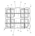
- FIG. 5 is a cross-sectional view taken along the line YY of the mother substrate shown in FIG.
- the frame portion 103 having the first main surface 101a and the base portion 102 having the second main surface 101b are integrated. It is a structure.
- the frame portion 103 includes a frame-shaped metallized layer 116 and a via conductor 117.
- the base 102 includes an external connecting conductor 105, a protruding portion 106, an inner layer conductor 107, an electrode pad 114, and a via conductor 117.
- the first main surface 101a constitutes a sealing surface to which the lid 115 is joined
- the second main surface 101b constitutes a mounting surface on the module substrate 301.
- a frame-shaped metallized layer 116 is located on the first main surface 101a, and after the electronic component 112 is mounted on the mounting portion 104, the lid 115 is joined on the frame-shaped metallized layer 116 by a brazing material to form an electronic component. 112 is hermetically sealed.
- the electronic component storage package 100 may be composed of a structure in which the frame portion 103 and the base portion 102 are formed of separate insulating layers, and the frame portion 103 and the base portion 102 are joined.
- the base 102 has a flat plate shape, and the mounting portion 104 on which the electronic component 112 is mounted is located in the central range on the side opposite to the second main surface 101b.
- FIG. 1 shows an example in which a crystal oscillator (piezoelectric element) is mounted as an electronic component 112.
- the insulating substrate 101 including the base portion 102 and the frame portion 103 is made of an insulating material.
- a ceramic material such as an aluminum oxide sintered body, an aluminum nitride sintered body, a mullite sintered body, or a glass-ceramic sintered body can be applied.
- the external connecting conductor 105 extends toward the second main surface 101b and is located on the second main surface 101b as a surface exposed to the outside. As shown in FIG. 3, for example, four external connecting conductors 105 are located on the base 102. As shown in FIG. 3, the external connecting conductor 105 has a four-sided planar shape and is located at the four corners of the base 102 on the second main surface 101b side.
- the inner layer conductor 107 is located inside the base 102 so as to face the external connecting conductor 105 as a surface. Further, as shown in FIG. 2, the inner layer conductor 107 is positioned so as to be inclined from the outer edge of the base portion 102 toward the center of the base portion 102 in cross-sectional perspective. Further, as shown in FIGS. 3 and 4, the end portion of the inner layer conductor 107 is exposed on the side surface of the base portion 102.
- the outer connecting conductor 105 and the inner layer conductor 107 have a smaller area in plan perspective than the inner layer conductor 107 and the portion corresponding to the second main surface 101b side of the insulating substrate 101 in the outer connecting conductor 105, and are located inside. It is connected by unit 106.
- the surrounding portion 108 is located in the region between the external connecting conductor 105 and the inner layer conductor 107 except for the protruding portion 106 of the external connecting conductor 105.
- the electrode pad 114 located at the mounting portion 104 is led out to one of the external connecting conductors 105 via the via conductor 117, the inner layer conductor 107, and the protruding portion 106.
- the frame-shaped metallized layer 116 located on the first main surface 101a of the frame portion 103 is led out to the other external connecting conductor 105 via the via conductor 117, the inner layer conductor 107, and the protruding portion 106.
- a relay conductor (not shown) may be positioned in the middle of the via conductor 117, and the via conductor 117 may be connected to the external connecting conductor 105 by the relay conductor.
- the two external connecting conductors 105 derived from the two electrode pads 114 are, for example, two externals located diagonally at the four corners of the base 102 among the four external connecting conductors 105 located on the second main surface 101b.
- the external connecting conductor 105 arranged on the connecting conductor 105 and derived from the frame-shaped metallized layer 116 is led out to the other two external connecting conductors 105 located diagonally at the four corners of the base 102.
- the electronic component storage package 100 of the present disclosure is located inside the insulating substrate 101 having a main surface, the external connecting conductor 105 whose main surface is partially exposed, and the insulating substrate 101 in the thickness direction of the external connecting conductor 105.
- the outer connecting conductor 105 has a protruding portion 106 toward the inner layer conductor 107, and the protruding portion 106 is in contact with the inner layer conductor 107.
- the protruding portion 106 of the external connecting conductor 105 bites into the insulating substrate 101, and the bonding strength of the external connecting conductor 105 to the insulating substrate 101 can be increased. That is, since the external connecting conductor 105 and the inner layer conductor 107 are arranged to face each other in a plane perspective, and the external connecting conductor 105 and the inner layer conductor 107 are connected by the protruding portion 106 of the external connecting conductor 105, the external connection is made. Since a part of the insulating substrate 101 is sandwiched between the conductor 105 and the inner layer conductor 107, the bonding strength between the insulating substrate 101 and the external connecting conductor 105 can be increased.
- the inner layer conductor 107 is located inside the base 102 so as to face the external connecting conductor 105. Further, the inner layer conductor 107 is positioned so as to incline from the outer edge of the base portion 102 toward the center of the base portion 102 in cross-sectional perspective. In the cross-sectional perspective, the end of the inner layer conductor 107 closest to the second main surface 101b is located closer to the first main surface 101a than the end of the external connecting conductor 105 closest to the first main surface 101a. There is. Then, the external connecting conductor 105 located on the second main surface 101b of the electronic component storage package 100 is connected to the module substrate 301 having the connecting pad 302 by a connecting member 303 such as solder.
- a connecting member 303 such as solder.
- the inner layer conductor 107 is positioned so as to be inclined from the outer edge of the base portion 102 to the central portion side of the base portion 102 in cross-sectional perspective, and is the farthest from the second main surface 101b at the four corners of the insulating substrate 101.
- the inner layer conductor 107 is a conduction path for connecting the conductors of the adjacent wiring board regions in the mother substrate 120 in which the wiring board regions (package 100 for storing electronic components) are arranged. Acts as. Therefore, by connecting the inner layer conductor 107 of one wiring board area and the inner layer conductor 107 of the other wiring board area across the boundary of the wiring board area, each conductor of one wiring board area and the other conductor 107 are connected.
- Each conductor in the wiring board area is integrated, and the entire conductor in the wiring board area arranged on the mother board 120 is electrically connected.
- Each conductor includes an external connecting conductor 105, a protrusion 106, an inner layer conductor 107, an electrode pad 114, a frame-shaped metallized layer 116, and a via conductor 117.
- the protrusion 106 is located inside the insulating substrate 101.
- the protruding portion 106 of the external connecting conductor 105 bites into the inside of the insulating substrate 101, and the bonding strength between the insulating substrate 101 and the external connecting conductor 105 can be further increased. That is, as shown in FIG. 3, the outer connecting conductor 105 and the inner layer conductor 107 are arranged to face each other in a plan perspective, and the outer connecting conductor 105 and the inner layer conductor 107 are connected by the protruding portion 106 of the outer connecting conductor 105.
- a part of the insulating substrate 101 is located between the external connecting conductor 105 and the inner layer conductor 107 so as to surround the protruding portion 106, and the stress in the plane direction with respect to the external connecting conductor 105 applied from the module substrate 301. Is dispersed by the protruding portion 106, so that the bonding strength of the external connecting conductor 105 to the insulating substrate 101 can be increased.
- four external connecting conductors 105 are arranged in a rectangular shape at the four corners of the insulating substrate 101, for example, in a plan perspective, and the protruding portions 106 are larger than the inner layer conductor 107 and the external connecting conductor 105. It has a small area and is located in a rectangular shape.
- the external connecting conductor 105 is exposed on the second main surface 101b side of the base 102 and the side surface of the base 102. Further, the outer peripheral end portion of the inner layer conductor 107 is exposed on the side surface of the base portion 102.
- the connecting member 303 that connects the external connecting conductor 105 of the electronic component storage package 100 and the connecting pad 302 of the module substrate 301 is the entire surface exposed on the second main surface 101b of the external connecting conductor 105 and the side surface of the base 102.
- the electronic component storage package 100 is firmly connected to the module board 301 by being connected to the portion exposed to.
- the inner layer conductor 107 is the connecting member 303. Do not contact with. Therefore, the volume of the connecting member 303 is suppressed from moving to the connecting conductor side including the external connecting conductor 105 of the electronic component storage package 100, so that the excessive connecting member 303 is short-circuited with the adjacent electronic device due to a fillet or the like. Etc. can be suppressed.
- the electronic component storage package 100 of the present disclosure has a surrounding portion 108 in which the insulating substrate 101 is sandwiched between the inner layer conductor 107 and the external connecting conductor 105 and is in contact with the protruding portion 106 in plan perspective.
- the connecting conductor located on the second main surface 101b side of the insulating substrate 101 is composed of the external connecting conductor 105, the protruding portion 106, and the inner layer conductor 107, the second main surface of the insulating substrate 101 in the external connecting conductor 105
- the thickness of the inner layer conductor 107 and the portion corresponding to the 101b side can be suppressed and positioned, and the influence of firing shrinkage on the mother substrate 120 when manufacturing the electronic component storage package 100 is reduced, and the insulating substrate 101 It is possible to provide a package 100 for storing electronic parts in which deformation is suppressed.
- outer connecting conductor 105 and the inner layer conductor 107 are connected by the protruding portion 106 on the central portion side of the outer connecting conductor 105, the outer connecting conductor 105 and the inner layer conductor 107 are firmly joined by the surrounding portion 108.
- the bonding strength of the external connecting conductor 105 to the insulating substrate 101 can be increased.
- the external connecting conductor 105 has four rectangular shapes located at the four corners of the insulating substrate 101 in a plan perspective, and the protruding portion 106 has a smaller area than the inner layer conductor 107 and the external connecting conductor 105, and is an example of a rectangular shape.
- the present invention is not limited to the above, and for example, a C surface is provided at one corner of one of the four external connecting conductors 105, and the external connecting conductor 105 having the above C surface is electron-generated. It may be used as an alignment mark of the component storage package 100, and the external connecting conductor 105 having a C surface may have a side portion 119 facing the center side of the insulating substrate 101.
- the external connecting conductor 105 may have a circular shape, a polygonal shape, a 1/4 circular shape, or the like in addition to the rectangular shape, and may be positioned by combining a plurality of shapes.
- the area of the protruding portion 106 connecting the outer connecting conductor 105 and the inner layer conductor 107 in the plan perspective is smaller than that of the outer connecting conductor 105 and the inner layer conductor 107, and the protruding portion 106 is the insulating substrate in the outer connecting conductor 105. It may be provided so as to be located between the portion corresponding to the second main surface 101b side of 101 and the inner layer conductor 107.
- the surrounding portion 108 surrounding the projecting portion 106 is located between the external connecting conductor 105 and the inner layer conductor 107, and the outer connecting conductor 105 and the inner layer conductor 107 are all around the external connecting conductor 105 by the surrounding portion 108.
- the bonding strength of the external connecting conductor 105 to the insulating substrate 101 can be increased.
- the exposed portion where the surrounding portion 108 corresponds to the side surface of the insulating substrate 101 has the uneven portion 109.
- the contact between the inner layer conductor 107 and the connecting member 303 can be suppressed more effectively. That is, since the uneven portion 109 prevents the volume of the connecting member 303 from moving to the inner layer conductor 107 side located on the side surface of the electronic component storage package 100, it is prevented from moving to the adjacent electronic device by the fillet or the like of the excessive connecting member 303. It is possible to suppress short circuits and the like.
- the connecting member 303 that connects the external connecting conductor 105 of the electronic component storage package 100 and the connecting pad 302 of the module substrate 301 is the entire surface exposed on the second main surface 101b of the external connecting conductor 105. And connected to the portion exposed on the side surface of the base 102, the electronic component storage package 100 is firmly connected to the module substrate 301, and the surface tension at the time of melting of the connecting member 303 crawls up the side surface of the insulating substrate 101. Try to get rid of.
- the uneven portion 109 can be formed of, for example, a fracture surface when the mother substrate 120 shown in FIGS. 5 and 6 is divided along a cut surface 110 located between the wiring board regions.
- the external connecting conductor 105 As shown in FIG. 4, if the thickness of the external connecting conductor 105 is thickened from the center side to the outer edge of the insulating substrate 101 in the side view, the external connecting conductor 105 and the module substrate 301 are connected. It is effective because it increases the bonding strength between the insulating substrate 101 and the external connecting conductor 105 at the outer edge of the insulating substrate 101 which is most susceptible to stress.
- the inner layer conductor 107 is exposed when the electronic component storage package 100 is manufactured from the mother substrate 120. Since it is difficult to connect the external connecting conductor 105 and the inner layer conductor 107 between adjacent wiring board regions in the plating process, it is possible to suppress a decrease in the divisibility of the mother substrate 120.
- the external connecting conductor 105 is located on the second main surface 101b, and the external connecting conductor 105 between the adjacent wiring board regions in the mother substrate 120 is already separated by the cut surface 110 before the division.
- the uneven portion 109 is located on the surrounding portion 108, it becomes difficult for the cut surface 110 to be located on the inclined inner layer conductor 107. Since most of the inner layer conductors 107 are located inside the base portion 102, it is difficult to provide the metal layer 111 on the inner layer conductor 107, and it is difficult for the adjacent inner layer conductors 107 to be connected to each other by the metal layer 111 in the plating process.
- the thickness of the portion of the surrounding portion 108 corresponding to the inside of the insulating substrate 101 is smaller than the thickness of the portion corresponding to the outside of the insulating substrate 101.
- the connecting conductor located on the second main surface 101b side of the insulating substrate 101 is composed of the outer connecting conductor 105, the protruding portion 106, and the inner layer conductor 107, and the outer connecting conductor 105 and the inner layer conductor 107 face each other in a plan perspective. Since the thickness of the surrounding portion 108 is smaller on the inside of the insulating substrate 101 than on the outside of the insulating substrate 101, the closer to the center of the insulating substrate 101 in the side perspective, the more the mounting portion 104 and the mounting portion 104 in the thickness direction are arranged.
- the electronic component storage package 100 in which the distance from the inner layer conductor 107 is increased, the influence of the firing shrinkage on the mounting portion 104 due to the thickness of the inner layer conductor 107 is suppressed, and the deformation of the mounting portion 104 of the insulating substrate 101 is suppressed. Can be provided.
- the insulating substrate 101 has a flat plate shape, and the mounting portion 104 on which the electronic component 112 is mounted is located on the side opposite to the second main surface 101b, and the mounted electrons.
- the component 112 is a crystal oscillator (piezoelectric element)
- a pair of electrode pads 114 are located at the corners of the mounting portion 104.
- the pair of electrode pads 114 are not horizontal, and even if the electrodes (not shown) of the electronic component 112 to be mounted are arranged to face the pair of electrode pads 114.
- the characteristics of the electronic component 112 may deteriorate, such as the electronic component 112 tilting or the thickness of the bonding material 113 becoming uneven. It is possible to provide an electronic component storage package 100 having excellent mounting reliability of the electronic component 112 in which deformation of the mounting portion 104 of the insulating substrate 101 is suppressed.
- the portion of the surrounding portion 108 located on the central side of the insulating substrate 101 is a curved portion bent toward the main surface side. Has 118.
- the mother substrate 120 shown in FIGS. 5 and 6 is used as an individual wiring board (package for storing electronic components).
- the inner layer conductor 107 is not divided all at once but is divided so as to be torn from the second main surface 101b side toward the first main surface 101a side. It is suppressed.
- a metallized paste serving as the inner layer conductor 107 is formed on the second main surface 101b side of each wiring board region of the ceramic green sheet serving as the base 102. Is applied by a screen printing method or the like, and the ceramic paste that becomes the surrounding portion 108 is applied to the second main surface 101b side of each wiring board area except for the central portion of the metallized paste that becomes the applied inner layer conductor 107. Then, the metallized paste to be the external connecting conductor 105 may be reapplied on the above ceramic paste by a screen printing method or the like, and then the second main surface 101b side of the processed ceramic green sheet may be pressurized.
- the surrounding portion 108 is deformed toward the inside of the insulating substrate 101 so that the thickness gradually decreases, and the curved portion 118 is located.
- the inner layer conductor 107 has an inclined configuration, and the inner layer conductor 107 is most separated from the second main surface 101b at the four corners of the insulating substrate 101, and the central portion side of the insulating substrate 101. That is, at the end of the inner layer conductor 107, the inner layer conductor 107 is closest to the second main surface 101b.
- the exposed surface of the external connecting conductor 105 is located on the same plane as the second main surface 101b.
- the inner layer conductor 107, the protruding portion 106, and the outer connecting conductor 105 may be positioned on the insulating substrate 101 by a press-fitting method or a plating method.
- the outer connecting conductor 105 and the inner layer conductor 107 are arranged so as to face each other in the cross-sectional perspective, and the outer connecting conductor 105 and the inner layer conductor 107 are further connected by the protruding portion 106 on the central portion side of the outer connecting conductor 105. Therefore, even if stress is applied from the connecting member 303 to the external connecting conductor 105, the stress can be dispersed to the surrounding portion 108 at the outer peripheral portion of the external connecting conductor 105, and the protruding portion 106 and the inner layer on the central portion side of the external connecting conductor 105. It can be dispersed in the conductor 107.
- the electronic component storage package 100 of the present disclosure has a side portion 119 in which the protruding portion 106 faces the center side of the insulating substrate 101 in plan perspective.
- the bonding strength of the external connecting conductor 105 to the insulating substrate 101 can be increased, and for example, a C surface is provided at one corner of one of the four external connecting conductors 105.
- the external connecting conductor 105 having the C surface of is used as an alignment mark of the electronic component storage package 100, the bonding strength of the external connecting conductor 105 to the insulating substrate 101 is increased even in the external connecting conductor 105 having the C surface. it can.
- the outer connecting conductor 105 and the inner layer conductor 107 are arranged to face each other in a plane perspective, and the outer connecting conductor 105 and the inner layer conductor 107 having a C surface are formed by the protruding portion 106 having the side portion 119.
- the insulating substrate 101 can be held between the outer connecting conductor 105 and the inner layer conductor 107, and the protruding portion 106 having the inner layer conductor 107 and the side portion 119 located inside the base portion 102 allows the C to be held.
- the connection between the wiring conductors with the external connecting conductor 105 having a surface can be strengthened.
- the second main surface 101b of the insulating substrate 101 has a C surface. Even if the external connecting conductor 105 is positioned, the outer edge of the protruding portion 106 located between the inner layer conductor 107 and the portion of the external connecting conductor 105 corresponding to the second main surface 101b side of the insulating substrate 101 is the external connecting conductor. Since it does not exceed the outer edge of 105, the surrounding portion 108 is located between the inner layer conductor 107 and the outer connecting conductor 105 over the entire circumference.
- connection between the wiring conductors to the external connecting conductor 105 having the C surface can be strengthened by the protruding portion 106 having the inner layer conductor 107 and the side portion 119 over the entire circumference of the external connecting conductor 105.
- the electronic component storage package 100 can be used as an alignment mark on the second main surface 101b of the electronic component storage package 100 while increasing the bonding strength of the external connecting conductor 105 to the insulating substrate 101.
- the external connecting conductor 105 having a C surface, defects during mounting of the electronic component 112 on the mounting portion 104 of the insulating substrate 101 are suppressed, and a package for storing the electronic component with excellent mounting reliability of the electronic component 112 is provided. Can be provided.
- the metal layer 111 is located on the exposed portion of the external connecting conductor 105 and the metal layer 111 is not located on the exposed portion of the inner layer conductor 107 on the side surface of the insulating substrate 101.
- the module substrate 301 can be satisfactorily connected to the connection pad 302, and since the metal layer 111 is not located on the exposed surface of the inner layer conductor 107, the connecting member 303 such as solder is formed as an inner layer. Crawling up to the conductor 107 side is suppressed, and the possibility of insufficient volume of the connecting member 303, short circuit with the adjacent electronic component 112, and the like can be suppressed.
- the metal layer 111 means a nickel plating layer, a gold plating layer, or the like provided on the surface of each of the other exposed wiring conductors including the external connecting conductor 105, and is exposed. It is sequentially adhered to the surface of each wiring conductor. Then, for example, the nickel plating layer is formed to be about 1.0 to 20 ⁇ m, and the gold plating layer is formed to be about 0.1 to 1.0 ⁇ m. Since the surface of each exposed wiring conductor is covered with the metal layer 111, the wiring conductor has excellent corrosion resistance and good wettability such as solder and brazing material.
- the metal layer 111 is not located on the exposed surface of the inner layer conductor 107, as shown in FIGS. 5 and 6, plating is performed on the mother substrate 120 in which the wiring board region serving as the electronic component storage package 100 is arranged. Since the inner layer conductor 107 is not exposed in the process and the plating solution does not come into contact with the inner layer conductor 107, the metal layer 111 is not adhered to the exposed surface of the inner layer conductor 107. Then, the inner layer conductor 107 acts as a conduction path for connecting the conductors in the adjacent wiring board region, and when the mother substrate 120 is divided, it is exposed as a fracture surface on the side surface of the electronic component storage package 100.
- the metal layer 111 is not located on the exposed surface of the inner layer conductor 107, and the surrounding portion 108 is located between the outer connecting conductor 105 and the inner layer conductor 107 so that the connecting member 303 such as solder does not get wet.
- the connecting member 303 crawls from the external connecting conductor 105 to the inner layer conductor 107 side beyond the surrounding portion 108. Therefore, it is possible to suppress the possibility of insufficient volume of the connecting member 303, short circuit with adjacent electronic components, and the like.
- the inner layer conductor 107 acts as a conduction path for connecting the conductors in the adjacent wiring board regions, and as shown in FIG. 4, if the inner layer conductor 107 is inclined, it is insulated. At the four corners of the substrate 101, the configuration is the farthest from the second main surface 101b. Then, when the mold and the cutter blade are pressed against the ceramic green sheet laminate to be the mother substrate 120 in order to position the cut surface 110 on the mother substrate 120, the cut surface 110 is positioned on the external connecting conductor 105 and the surrounding portion 108. At the same time, since the cut surface 110 is located on the end side of the inner layer conductor 107, it is difficult to cut the inner layer conductor 107 on the four corner sides of the insulating substrate 101. Therefore, conduction paths are secured on the four corners of the insulating substrate 101, and the metal layer 111 can be satisfactorily positioned on the exposed conductor of each wiring board region of the mother substrate 120 by the plating step.
- the cut surface 110 may be positioned by a laser at the boundary of the wiring board region. In the above case, the non-contact processing is performed, and the ceramic green sheet laminate is not deformed by pressing the mold or the like.
- a metal layer 111 such as a nickel layer and a gold layer is sequentially provided on the surface of an exposed conductor such as an external connecting conductor 105, an electrode pad 114, and a frame-shaped metallized layer 116. Since the surface of each exposed conductor is covered by the metal layer 111, it is possible to realize a package for storing electronic components having a conductor having excellent corrosion resistance and good wettability such as solder and brazing material.
- the electronic device 200 of the present disclosure includes the electronic component storage package 100 described in any of the above, and the electronic component 112 mounted on the electronic component storage package 100. With the above configuration, it is possible to provide an electronic device 200 having excellent connection reliability to the module substrate 301 by using the electronic component storage package 100 having a high bonding strength of the external connecting conductor 105 to the insulating substrate 101.
- the external connecting conductor 105 and the inner layer conductor 107 are arranged to face each other in a plan view, and the external connecting conductor 105 and the inner layer conductor 107 are further connected by the protruding portion 106.
- the external connecting conductor 105 and the inner layer conductor 107 are firmly joined to the insulating substrate 101 including the surrounding portion 108.
- the connection between the wiring conductors of the inner layer conductor 107 located inside the base 102 and the external connecting conductor 105 is strengthened by the protruding portion 106, and the insulating substrate 101 is connected to the insulating substrate 101.
- the outer connecting conductor 105 and the inner layer conductor 107 are exposed on the long side side surface and the short side side side surface of the electronic device 200, and the outer connecting conductor 105 and the inner layer conductor 107 The surrounding part 108 is located between them.
- a metal layer 111 such as a nickel layer or a gold layer is located on the exposed entire surface of the external connecting conductor 105. Further, if the metal layer 111 is not located on the exposed surface of the inner layer conductor 107, the solder does not easily get wet with the inner layer conductor 107 when the electronic device 200 is mounted on the module substrate 301.
- the electronic module 300 of the present disclosure has a module board 301 having a connection pad 302 and the electronic device 200 described above to which the connection pad 302 is connected. With the above configuration, it is possible to provide the electronic module 300 having high reliability of electrical characteristics by using the electronic device 200 having excellent connection reliability to the module substrate 301. That is, in the electronic device 200, the external connecting conductor 105 and the inner layer conductor 107 are arranged to face each other in a plan perspective, and the external connecting conductor 105 and the inner layer conductor 107 are further connected by a protruding portion 106, so that the external connecting conductor 105 is connected. And the inner layer conductor 107 includes a package 100 for storing electronic components firmly bonded to an insulating substrate 101 including a surrounding portion 108.
- the connection between the wiring conductors of the inner layer conductor 107 located inside the base 102 and the external connecting conductor 105 is strengthened by the protruding portion 106, and the insulating substrate 101
- an electronic device 200 having excellent bonding strength of the external connecting conductor 105 to and having excellent connection reliability it is possible to provide an electronic module 300 having high reliability of electrical characteristics.
- the external connecting conductor 105 is not located extending from the second main surface 101b of the insulating substrate 101 to the side surface, and the electronic device 200 is connected to the connecting pad of the module substrate 301.
- the side surface of the electronic device 200 which has become smaller and lighter, is pulled by the surface tension of the solder (connecting member 303), and the electronic device 200 stands up and mounts due to the Manhattan phenomenon. It is suppressed that it becomes defective.
- the electronic device 200 in which the electronic component 112 is mounted on the electrode pad 114 of the mounting portion 104 can be realized, and the bonding strength between the electronic device 200 and the module substrate 301 can be realized. It is possible to provide an electronic module 300 having excellent connection reliability while suppressing a decrease in the voltage.
- the present invention is not limited to the above embodiment.
- four external connecting conductors 105 are positioned at the four corners of the base 102 of the insulating substrate 101 on the second main surface 101b side, but depending on the type and shape of the electronic device, etc. External connecting conductors other than the four may be positioned.
- the example in which the external connecting conductor 105 is located at a position where it is in contact with both the short side side and the long side side of the insulating substrate 101 is shown, a place where it is in contact with only the short side side or only the long side side of the insulating substrate 101. It may be located at.
- the surrounding portion 108 is located between the outer connecting conductor 105 and the inner layer conductor 107.
- the electronic component storage package 100 having the base 102 and the frame portion 103 is shown as a configuration having the wiring board according to the present invention.
- the electronic component storage package of the present invention is the frame portion. It may have a flat plate-like structure without any.
- an example in which a crystal oscillator is mounted as an electronic component is shown, but the electronic component can be applied to various modified examples such as a semiconductor element, a capacitor, an inductor, and a resistor.
- the details shown in the embodiment can be appropriately changed without departing from the spirit of the invention.
Landscapes
- Physics & Mathematics (AREA)
- Acoustics & Sound (AREA)
- Piezo-Electric Or Mechanical Vibrators, Or Delay Or Filter Circuits (AREA)
Priority Applications (4)
| Application Number | Priority Date | Filing Date | Title |
|---|---|---|---|
| CN202080044803.0A CN114026785B (zh) | 2019-06-27 | 2020-06-24 | 电子部件收纳用封装件、电子装置以及电子模块 |
| US17/620,837 US12470200B2 (en) | 2019-06-27 | 2020-06-24 | Electronic component housing package, electronic device, and electronic module |
| JP2021527698A JP7182712B2 (ja) | 2019-06-27 | 2020-06-24 | 電子部品収納用パッケージ、電子装置、および電子モジュール |
| EP20832979.7A EP3993024A4 (en) | 2019-06-27 | 2020-06-24 | ELECTRONIC COMPONENT BOX, ELECTRONIC DEVICE AND ELECTRONIC MODULE |
Applications Claiming Priority (2)
| Application Number | Priority Date | Filing Date | Title |
|---|---|---|---|
| JP2019120065 | 2019-06-27 | ||
| JP2019-120065 | 2019-06-27 |
Publications (1)
| Publication Number | Publication Date |
|---|---|
| WO2020262472A1 true WO2020262472A1 (ja) | 2020-12-30 |
Family
ID=74060142
Family Applications (1)
| Application Number | Title | Priority Date | Filing Date |
|---|---|---|---|
| PCT/JP2020/024858 Ceased WO2020262472A1 (ja) | 2019-06-27 | 2020-06-24 | 電子部品収納用パッケージ、電子装置、および電子モジュール |
Country Status (5)
| Country | Link |
|---|---|
| US (1) | US12470200B2 (https=) |
| EP (1) | EP3993024A4 (https=) |
| JP (1) | JP7182712B2 (https=) |
| CN (1) | CN114026785B (https=) |
| WO (1) | WO2020262472A1 (https=) |
Cited By (1)
| Publication number | Priority date | Publication date | Assignee | Title |
|---|---|---|---|---|
| WO2022163502A1 (ja) * | 2021-01-27 | 2022-08-04 | 京セラ株式会社 | 電子部品収納用パッケージ、電子装置および電子モジュール |
Citations (4)
| Publication number | Priority date | Publication date | Assignee | Title |
|---|---|---|---|---|
| JP2002164451A (ja) | 2000-11-28 | 2002-06-07 | Kyocera Corp | 電子部品収納用パッケージ |
| JP2017063165A (ja) * | 2015-09-26 | 2017-03-30 | 京セラ株式会社 | 電子部品収納用パッケージ、電子装置および電子モジュール |
| WO2017090508A1 (ja) * | 2015-11-25 | 2017-06-01 | 京セラ株式会社 | 電子部品収納用パッケージ、電子装置および電子モジュール |
| JP2018032773A (ja) * | 2016-08-25 | 2018-03-01 | 京セラ株式会社 | 電子部品搭載用基板、電子装置および電子モジュール |
Family Cites Families (9)
| Publication number | Priority date | Publication date | Assignee | Title |
|---|---|---|---|---|
| US5789278A (en) * | 1996-07-30 | 1998-08-04 | Micron Technology, Inc. | Method for fabricating chip modules |
| US6740960B1 (en) * | 1997-10-31 | 2004-05-25 | Micron Technology, Inc. | Semiconductor package including flex circuit, interconnects and dense array external contacts |
| JP4111222B2 (ja) * | 2003-07-22 | 2008-07-02 | 株式会社村田製作所 | 表面実装型部品 |
| WO2008053956A1 (fr) * | 2006-11-02 | 2008-05-08 | Murata Manufacturing Co., Ltd. | Substrat en céramique, dispositif électronique et procédé de production d'un substrat en céramique |
| CN106458761B (zh) | 2014-03-19 | 2019-08-06 | 日本碍子株式会社 | 陶瓷基体及其制造方法 |
| WO2017126596A1 (ja) * | 2016-01-22 | 2017-07-27 | 京セラ株式会社 | 電子部品収納用パッケージ、多数個取り配線基板、電子装置および電子モジュール |
| JP6677547B2 (ja) * | 2016-03-23 | 2020-04-08 | 京セラ株式会社 | 電子部品収納用パッケージ、電子装置および電子モジュール |
| JP6767772B2 (ja) * | 2016-04-28 | 2020-10-14 | Ngkエレクトロデバイス株式会社 | 電子部品収納用パッケージおよびそれを用いた電子装置 |
| US11515242B2 (en) * | 2017-12-28 | 2022-11-29 | Kyocera Corporation | Wiring substrate, electronic device, and electronic module each having plate-shaped conductive portion in frame portion of insulation substrate |
-
2020
- 2020-06-24 CN CN202080044803.0A patent/CN114026785B/zh active Active
- 2020-06-24 US US17/620,837 patent/US12470200B2/en active Active
- 2020-06-24 JP JP2021527698A patent/JP7182712B2/ja active Active
- 2020-06-24 EP EP20832979.7A patent/EP3993024A4/en active Pending
- 2020-06-24 WO PCT/JP2020/024858 patent/WO2020262472A1/ja not_active Ceased
Patent Citations (4)
| Publication number | Priority date | Publication date | Assignee | Title |
|---|---|---|---|---|
| JP2002164451A (ja) | 2000-11-28 | 2002-06-07 | Kyocera Corp | 電子部品収納用パッケージ |
| JP2017063165A (ja) * | 2015-09-26 | 2017-03-30 | 京セラ株式会社 | 電子部品収納用パッケージ、電子装置および電子モジュール |
| WO2017090508A1 (ja) * | 2015-11-25 | 2017-06-01 | 京セラ株式会社 | 電子部品収納用パッケージ、電子装置および電子モジュール |
| JP2018032773A (ja) * | 2016-08-25 | 2018-03-01 | 京セラ株式会社 | 電子部品搭載用基板、電子装置および電子モジュール |
Cited By (2)
| Publication number | Priority date | Publication date | Assignee | Title |
|---|---|---|---|---|
| WO2022163502A1 (ja) * | 2021-01-27 | 2022-08-04 | 京セラ株式会社 | 電子部品収納用パッケージ、電子装置および電子モジュール |
| JP7536900B2 (ja) | 2021-01-27 | 2024-08-20 | 京セラ株式会社 | 電子部品収納用パッケージ、電子装置および電子モジュール |
Also Published As
| Publication number | Publication date |
|---|---|
| CN114026785A (zh) | 2022-02-08 |
| US12470200B2 (en) | 2025-11-11 |
| JP7182712B2 (ja) | 2022-12-02 |
| US20220385266A1 (en) | 2022-12-01 |
| EP3993024A4 (en) | 2023-08-09 |
| JPWO2020262472A1 (https=) | 2020-12-30 |
| EP3993024A1 (en) | 2022-05-04 |
| CN114026785B (zh) | 2025-07-22 |
Similar Documents
| Publication | Publication Date | Title |
|---|---|---|
| JP6671441B2 (ja) | 電子部品収納用パッケージ、多数個取り配線基板、電子装置および電子モジュール | |
| JP5853429B2 (ja) | 電子部品用パッケージおよび圧電振動デバイス | |
| JP5741578B2 (ja) | 圧電振動デバイスの封止部材、および圧電振動デバイス | |
| JP7075810B2 (ja) | 電子部品収納用パッケージ、電子装置、および電子モジュール | |
| TWI822418B (zh) | 搭載熱敏電阻的壓電振動裝置 | |
| CN111512432B (zh) | 布线基板、电子装置以及电子模块 | |
| JP7182712B2 (ja) | 電子部品収納用パッケージ、電子装置、および電子モジュール | |
| CN113692644B (zh) | 电子部件收纳用封装件、电子装置以及电子模块 | |
| JP6813682B2 (ja) | 電子部品収納用パッケージ、電子装置および電子モジュール | |
| JP4404684B2 (ja) | 配線基板 | |
| WO2015012405A1 (ja) | 素子収納用パッケージおよび実装構造体 | |
| JP6677547B2 (ja) | 電子部品収納用パッケージ、電子装置および電子モジュール | |
| JPWO2019146658A1 (ja) | 配線基板、電子装置及び電子モジュール | |
| JP2015029201A (ja) | 圧電振動素子搭載用基板および圧電装置 | |
| JP6321477B2 (ja) | 電子部品収納用パッケージ、パッケージ集合体および電子部品収納用パッケージの製造方法 | |
| JP2005244146A (ja) | 電子部品収納用パッケージおよび電子装置ならびに電子装置の実装構造 | |
| JP4511335B2 (ja) | 多数個取り配線基板および電子装置 | |
| JP2007242908A (ja) | 電子部品収納用セラミックパッケージ | |
| JP5468327B2 (ja) | 圧電デバイス | |
| JP2005340561A (ja) | 配線基板 | |
| JP2021158191A (ja) | セラミック製のキャップ及び圧電デバイス | |
| JP2004022893A (ja) | 配線基板 | |
| JP2019134063A (ja) | 配線基板、電子装置及び電子モジュール | |
| JP2005210522A (ja) | 圧電振動子収納用パッケージおよび圧電装置 | |
| JP2012134301A (ja) | 配線基板 |
Legal Events
| Date | Code | Title | Description |
|---|---|---|---|
| 121 | Ep: the epo has been informed by wipo that ep was designated in this application |
Ref document number: 20832979 Country of ref document: EP Kind code of ref document: A1 |
|
| ENP | Entry into the national phase |
Ref document number: 2021527698 Country of ref document: JP Kind code of ref document: A |
|
| NENP | Non-entry into the national phase |
Ref country code: DE |
|
| WWE | Wipo information: entry into national phase |
Ref document number: 2020832979 Country of ref document: EP |
|
| ENP | Entry into the national phase |
Ref document number: 2020832979 Country of ref document: EP Effective date: 20220127 |
|
| WWG | Wipo information: grant in national office |
Ref document number: 202080044803.0 Country of ref document: CN |
|
| WWG | Wipo information: grant in national office |
Ref document number: 17620837 Country of ref document: US |