WO2020261817A1 - 固体撮像素子、固体撮像素子の製造方法 - Google Patents
固体撮像素子、固体撮像素子の製造方法 Download PDFInfo
- Publication number
- WO2020261817A1 WO2020261817A1 PCT/JP2020/019711 JP2020019711W WO2020261817A1 WO 2020261817 A1 WO2020261817 A1 WO 2020261817A1 JP 2020019711 W JP2020019711 W JP 2020019711W WO 2020261817 A1 WO2020261817 A1 WO 2020261817A1
- Authority
- WO
- WIPO (PCT)
- Prior art keywords
- electrode
- forming
- dielectric film
- solid
- capacitor
- Prior art date
- Legal status (The legal status is an assumption and is not a legal conclusion. Google has not performed a legal analysis and makes no representation as to the accuracy of the status listed.)
- Ceased
Links
Images















Classifications
-
- H—ELECTRICITY
- H10—SEMICONDUCTOR DEVICES; ELECTRIC SOLID-STATE DEVICES NOT OTHERWISE PROVIDED FOR
- H10F—INORGANIC SEMICONDUCTOR DEVICES SENSITIVE TO INFRARED RADIATION, LIGHT, ELECTROMAGNETIC RADIATION OF SHORTER WAVELENGTH OR CORPUSCULAR RADIATION
- H10F39/00—Integrated devices, or assemblies of multiple devices, comprising at least one element covered by group H10F30/00, e.g. radiation detectors comprising photodiode arrays
- H10F39/80—Constructional details of image sensors
- H10F39/803—Pixels having integrated switching, control, storage or amplification elements
- H10F39/8037—Pixels having integrated switching, control, storage or amplification elements the integrated elements comprising a transistor
-
- H—ELECTRICITY
- H10—SEMICONDUCTOR DEVICES; ELECTRIC SOLID-STATE DEVICES NOT OTHERWISE PROVIDED FOR
- H10D—INORGANIC ELECTRIC SEMICONDUCTOR DEVICES
- H10D1/00—Resistors, capacitors or inductors
- H10D1/60—Capacitors
- H10D1/68—Capacitors having no potential barriers
- H10D1/692—Electrodes
- H10D1/711—Electrodes having non-planar surfaces, e.g. formed by texturisation
- H10D1/716—Electrodes having non-planar surfaces, e.g. formed by texturisation having vertical extensions
-
- H—ELECTRICITY
- H10—SEMICONDUCTOR DEVICES; ELECTRIC SOLID-STATE DEVICES NOT OTHERWISE PROVIDED FOR
- H10D—INORGANIC ELECTRIC SEMICONDUCTOR DEVICES
- H10D84/00—Integrated devices formed in or on semiconductor substrates that comprise only semiconducting layers, e.g. on Si wafers or on GaAs-on-Si wafers
-
- H—ELECTRICITY
- H10—SEMICONDUCTOR DEVICES; ELECTRIC SOLID-STATE DEVICES NOT OTHERWISE PROVIDED FOR
- H10D—INORGANIC ELECTRIC SEMICONDUCTOR DEVICES
- H10D84/00—Integrated devices formed in or on semiconductor substrates that comprise only semiconducting layers, e.g. on Si wafers or on GaAs-on-Si wafers
- H10D84/01—Manufacture or treatment
- H10D84/02—Manufacture or treatment characterised by using material-based technologies
- H10D84/03—Manufacture or treatment characterised by using material-based technologies using Group IV technology, e.g. silicon technology or silicon-carbide [SiC] technology
- H10D84/038—Manufacture or treatment characterised by using material-based technologies using Group IV technology, e.g. silicon technology or silicon-carbide [SiC] technology using silicon technology, e.g. SiGe
-
- H—ELECTRICITY
- H10—SEMICONDUCTOR DEVICES; ELECTRIC SOLID-STATE DEVICES NOT OTHERWISE PROVIDED FOR
- H10F—INORGANIC SEMICONDUCTOR DEVICES SENSITIVE TO INFRARED RADIATION, LIGHT, ELECTROMAGNETIC RADIATION OF SHORTER WAVELENGTH OR CORPUSCULAR RADIATION
- H10F39/00—Integrated devices, or assemblies of multiple devices, comprising at least one element covered by group H10F30/00, e.g. radiation detectors comprising photodiode arrays
- H10F39/011—Manufacture or treatment of image sensors covered by group H10F39/12
- H10F39/014—Manufacture or treatment of image sensors covered by group H10F39/12 of CMOS image sensors
-
- H—ELECTRICITY
- H10—SEMICONDUCTOR DEVICES; ELECTRIC SOLID-STATE DEVICES NOT OTHERWISE PROVIDED FOR
- H10F—INORGANIC SEMICONDUCTOR DEVICES SENSITIVE TO INFRARED RADIATION, LIGHT, ELECTROMAGNETIC RADIATION OF SHORTER WAVELENGTH OR CORPUSCULAR RADIATION
- H10F39/00—Integrated devices, or assemblies of multiple devices, comprising at least one element covered by group H10F30/00, e.g. radiation detectors comprising photodiode arrays
- H10F39/10—Integrated devices
- H10F39/12—Image sensors
-
- H—ELECTRICITY
- H10—SEMICONDUCTOR DEVICES; ELECTRIC SOLID-STATE DEVICES NOT OTHERWISE PROVIDED FOR
- H10F—INORGANIC SEMICONDUCTOR DEVICES SENSITIVE TO INFRARED RADIATION, LIGHT, ELECTROMAGNETIC RADIATION OF SHORTER WAVELENGTH OR CORPUSCULAR RADIATION
- H10F39/00—Integrated devices, or assemblies of multiple devices, comprising at least one element covered by group H10F30/00, e.g. radiation detectors comprising photodiode arrays
- H10F39/10—Integrated devices
- H10F39/12—Image sensors
- H10F39/199—Back-illuminated image sensors
-
- H—ELECTRICITY
- H10—SEMICONDUCTOR DEVICES; ELECTRIC SOLID-STATE DEVICES NOT OTHERWISE PROVIDED FOR
- H10F—INORGANIC SEMICONDUCTOR DEVICES SENSITIVE TO INFRARED RADIATION, LIGHT, ELECTROMAGNETIC RADIATION OF SHORTER WAVELENGTH OR CORPUSCULAR RADIATION
- H10F39/00—Integrated devices, or assemblies of multiple devices, comprising at least one element covered by group H10F30/00, e.g. radiation detectors comprising photodiode arrays
- H10F39/80—Constructional details of image sensors
- H10F39/811—Interconnections
Definitions
- the technique (the present technique) according to the present disclosure relates to, for example, a back-illuminated solid-state image sensor and a method for manufacturing the solid-state image sensor.
- a configuration is used in which a capacitor is formed under a photodiode with a MIS (Metal Insulator Silicon) structure with reference to incident light.
- MIS Metal Insulator Silicon
- the area for arranging the capacitor is reduced, which is necessary to obtain the capacity required for the capacitor. It is difficult to secure the occupied area.
- the second semiconductor substrate is formed.
- a technique for forming a trench capacitor With the technique disclosed in Patent Document 1, it is possible to secure the area of the capacitor without reducing the area.
- Patent Document 1 After forming a trench capacitor on the second semiconductor substrate, the first semiconductor substrate and the second semiconductor substrate are laminated to form a solid-state image sensor. Therefore, there is a problem that many dedicated steps are required to form the trench capacitor, and the number of steps required for manufacturing increases.
- the solid-state image sensor includes a semiconductor substrate, a capacitor, an amplification transistor, and an FD side wiring electrode.
- the semiconductor substrate includes a photodiode that photoelectrically converts the incident light and a floating diffusion in which the signal charge accumulated in the photodiode is transferred.
- the capacitor has a PD-side electrode arranged on a surface opposite to the surface on which the light of the photodiode is incident, and an anti-PD-side electrode facing the PD-side electrode with a dielectric film in between.
- the amplification transistor reads out the signal charge transferred to the floating diffusion as an electric signal and amplifies it.
- the FD side wiring electrode connects the floating diffusion and the amplification transistor.
- At least a part of the PD side electrode and the FD side wiring electrode are formed in a shape extending in the semiconductor substrate along the thickness direction of the semiconductor substrate. Further, one end of the first contact hole that forms at least a part of the PD side electrode inside and one end of the second contact hole that forms the FD side wiring electrode inside are both surfaces opposite to the photodiode side of the semiconductor substrate. Is located in.
- a method for manufacturing a solid-state image sensor is a step of forming a photodiode that photoelectrically converts incident light and a floating diffusion to which signal charges accumulated in the photodiode are transferred on a semiconductor substrate.
- the present invention comprises a step of forming a capacitor having a PD side electrode arranged on a surface opposite to the surface on which the light of the photodiode is incident, and an anti-PD side electrode facing the PD side electrode with a dielectric film sandwiched between them. ..
- a step of forming an amplification transistor that reads out and amplifies the signal charge transferred to the floating diffusion as an electric signal is provided.
- a method for manufacturing a solid-state image sensor is a step of forming a photodiode that photoelectrically converts incident light and a floating diffusion to which signal charges accumulated in the photodiode are transferred on a semiconductor substrate. To be equipped with.
- the present invention comprises a step of forming a capacitor having a PD side electrode arranged on a surface opposite to the surface on which the light of the photodiode is incident, and an anti-PD side electrode facing the PD side electrode with a dielectric film sandwiched between them. ..
- a step of forming an amplification transistor that reads out and amplifies the signal charge transferred to the floating diffusion as an electric signal is provided. Then, in the step of forming the capacitor, the first contact hole that forms at least a part of the PD side electrode inside and the second contact hole that forms the FD side wiring electrode that connects the floating diffusion and the amplification transistor are formed inside.
- a method for manufacturing a solid-state image sensor is a step of forming a photodiode that photoelectrically converts incident light and a floating diffusion to which signal charges accumulated in the photodiode are transferred on a semiconductor substrate.
- the present invention comprises a step of forming a capacitor having a PD side electrode arranged on a surface opposite to the surface on which the light of the photodiode is incident, and an anti-PD side electrode facing the PD side electrode with a dielectric film sandwiched between them. ..
- a step of forming an amplification transistor that reads out and amplifies the signal charge transferred to the floating diffusion as an electric signal is provided. Then, the PD side electrode is formed in the first contact hole that forms at least a part of the PD side electrode inside, and the FD side wiring electrode that connects the floating diffusion and the amplification transistor is formed in the second contact hole. Includes a step of simultaneously forming the FD side wiring electrode.
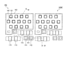
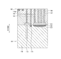
- FIG. 2 is a sectional view taken along line IV-IV of FIG. It is sectional drawing which shows the manufacturing method of the solid-state image sensor which concerns on 1st Embodiment. It is sectional drawing which shows the manufacturing method of the solid-state image sensor which concerns on 1st Embodiment.
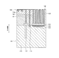
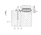
- the solid-state image sensor according to the first embodiment is, for example, a back-illuminated solid-state image sensor. As shown in FIGS. 1 to 4, the solid-state image sensor includes a semiconductor substrate including a first semiconductor substrate 101 and a second semiconductor substrate 102.
- the first semiconductor substrate 101 is a substrate on which a pixel circuit including a photodiode 110 and a floating diffusion 111 is arranged.
- the second semiconductor substrate 102 is a substrate laminated on the surface (upper surface in FIG. 4) opposite to the photodiode 110 side of the first semiconductor substrate 101. Note that FIG. 2 illustrates the second semiconductor substrate 102NP of adjacent pixels.
- the fifth electrode 163 is formed on the surface of the second semiconductor substrate 102 opposite to the surface facing the first semiconductor substrate 101 (the upper surface in FIG. 4).
- the fifth electrode 163 is formed by using, for example, a polycrystalline silicon film. Further, the fifth electrode 163 forms a wiring that constitutes an equivalent circuit of the solid-state image sensor.
- the photodiode 110 photoelectrically converts the incident light, and generates and stores an electric charge corresponding to the amount of light of the photoelectric conversion.
- One end of the photodiode 110 is grounded.
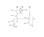
- the other end of the photodiode 110 is connected to the source electrode of the transfer transistor 112.
- the floating diffusion 111 is formed at a point (connection point) where the drain electrode of the transfer transistor 112, the source electrode of the switch transistor 115, and the gate electrode of the amplification transistor 114 are connected. Further, the floating diffusion 111 accumulates the electric charge transferred from the photodiode 110 via the transfer transistor 112 and converts it into a voltage. That is, the signal charge accumulated in the photodiode 110 is transferred to the floating diffusion 111.
- the transfer transistor 112 is arranged between the photodiode 110 and the floating diffusion 111.
- the drain electrode of the transfer transistor 112 is connected to the drain electrode of the reset transistor 113 and the gate electrode of the amplification transistor 114. Further, the transfer transistor 112 turns on or off the transfer of electric charge from the photodiode 110 to the floating diffusion 111 according to a drive signal supplied from the timing control unit (not shown) to the gate electrode.
- the switch transistor 115 is arranged between the floating diffusion 111 and the reset transistor 113.
- the drain electrode of the switch transistor 115 is connected to the source electrode of the reset transistor 113 and the capacitor 120. Further, the switch transistor 115 turns on or off the transfer of electric charge from the capacitor 120 to the floating diffusion 111 according to the switching signal supplied from the switching control unit (not shown) to the gate electrode.
- the capacitor 120 has a PD side electrode 130, a dielectric film 140, and an anti-PD side electrode 150.
- the PD side electrode 130 is an electrode arranged on a surface opposite to the surface on which the light of the photodiode 110 is incident.
- the anti-PD side electrode 150 is an electrode that faces the PD side electrode 130 with the dielectric film 140 sandwiched between them.
- the capacitor 120 includes a first capacitor unit 121 and a second capacitor unit 122.
- the first capacitor unit 121 is a capacitor formed in a first capacitor region preset on the first semiconductor substrate 101.
- the first capacitor region is set at a position different from the position where the floating diffusion 111 of the first semiconductor substrate 101 is arranged.
- the first capacitor portion 121 has a first electrode 131, a first dielectric film 141, and a second electrode 151.
- the first electrode 131 is an electrode arranged on a surface opposite to the surface on which the light of the photodiode 110 in the first capacitor region is incident.
- the first electrode 131 and the floating diffusion 111 are formed so as to be separated from each other. Further, the first electrode 131 is formed by using phosphorus or arsenic ion-implanted into the first capacitor region.
- the first dielectric film 141 is laminated on the first electrode 131. Further, the first dielectric film 141 is formed by using a silicon oxide film.
- the second electrode 151 is laminated on the first dielectric film 141. Further, the second electrode 151 is formed by using a polycrystalline silicon film.
- the second capacitor section 122 is a capacitor arranged on the surface of the first capacitor section 121 opposite to the photodiode 110 side.
- the second capacitor portion 122 has a third electrode 132, a second dielectric film 142, and a fourth electrode 152.
- the third electrode 132 is a columnar electrode that forms the PD side electrode 130 and one end (lower end in FIG. 4) is connected to the second electrode 151. Further, the third electrode 132 is formed by using a refractory metal such as tungsten, titanium nitride, cobalt, and ruthenium. The refractory metal is, for example, a metal having a melting point equal to or higher than the melting point of iron. Further, the third electrode 132 is formed inside the first contact hole 160.
- the first contact hole 160 is a gap portion formed in a semiconductor substrate (first semiconductor substrate 101, second semiconductor substrate 102) in a shape extending along the thickness direction of the semiconductor substrate. Therefore, the third electrode 132 forming the PD side electrode 130 is formed inside the first contact hole 160. That is, at least a part of the PD side electrode 130 is formed inside the first contact hole 160 and is formed in the semiconductor substrate in a shape extending along the thickness direction of the semiconductor substrate.
- a part of the third electrode 132 forming the PD side electrode 130 is formed inside the first semiconductor substrate 101, and the rest is formed inside the second semiconductor substrate 102.
- a part of the first contact hole 160 is formed inside the first semiconductor substrate 101, and the rest of the first contact hole 160 is formed inside the second semiconductor substrate 102.
- the second dielectric film 142 covers the portion other than the portion (the side surface and the upper surface of the third electrode 132) that forms the dielectric film 140 and is connected to the second electrode 151 of the third electrode 132. Therefore, a part of the second dielectric film 142 is formed inside the first semiconductor substrate 101, and the rest of the second dielectric film 142 is formed inside the second semiconductor substrate 102. Further, the second dielectric film 142 is formed by using a ferroelectric film.
- a laminated film of an oxide film and a nitride film As the strong dielectric film, a laminated film of an oxide film and a nitride film, a laminated film of an oxide film and a tantalum pentoxide film, a laminated film of a nitride film and a tantalum pentoxide film, and a laminated film of an oxide film, a nitride film and a tantalum pentaoxide film
- Membranes, hafnium and hafnium alloy materials, BST, PZT and the like can be used.
- the fourth electrode 152 is an electrode that forms the anti-PD side electrode 150 and faces the third electrode 132 with the second dielectric film 142 sandwiched between them. Further, the fourth electrode 152 is formed by using a refractory metal such as tungsten, titanium nitride, cobalt, and ruthenium, like the third electrode 132.
- the solid-state image sensor includes an FD side wiring electrode 161 that connects the floating diffusion 111 and the amplification transistor 114.
- the FD side wiring electrode 161 is formed inside the second contact hole 162. Further, the FD side wiring electrode 161 is formed by using a refractory metal such as tungsten, titanium nitride, cobalt, and ruthenium, like the third electrode 132.
- the second contact hole 162 is a gap portion formed inside the semiconductor substrate (first semiconductor substrate 101, second semiconductor substrate 102) in a shape extending along the thickness direction of the semiconductor substrate. Therefore, a part of the FD side wiring electrode 161 is formed inside the first semiconductor substrate 101, and the remaining part of the FD side wiring electrode 161 is formed inside the second semiconductor substrate 102. Further, the FD side wiring electrode 161 is formed in the semiconductor substrate in a shape extending along the thickness direction of the semiconductor substrate. Further, one end of the first contact hole 160 and one end of the second contact hole 162 (both of which are the upper open ends in FIG. 4) are photographs of semiconductor substrates (first semiconductor substrate 101 and second semiconductor substrate 102). It is located on the surface opposite to the diode 110 side.
- the source electrode is connected to the switch transistor 115, and the drain electrode is connected to the power supply wiring VDD. Further, the reset transistor 113 turns on or off the discharge of the electric charge accumulated in the floating diffusion 111 according to the drive signal supplied from the timing control unit to the gate electrode.
- the gate electrode is connected to the floating diffusion 111, and the source electrode is connected to the power supply wiring VDD.
- the drain electrode of the amplification transistor 114 is connected to the source electrode of the selection transistor 116.
- the amplification transistor 114 reads out the potential of the floating diffusion 111 reset by the reset transistor 113 as a reset level.
- the amplification transistor 114 amplifies the voltage corresponding to the signal charge stored in the floating diffusion 111 to which the signal charge is transferred by the transfer transistor 112. That is, the amplification transistor 114 reads out the signal charge transferred to the floating diffusion 111 as an electric signal and amplifies it.
- the voltage (voltage signal) amplified by the amplification transistor 114 is output to the vertical signal line VL via the selection transistor 116.
- the floating diffusion 111 and the amplification transistor 114 are connected by the FD side wiring electrode 161.
- the drain electrode is connected to one end of the vertical signal line VL, and the source electrode is connected to the drain electrode of the amplification transistor 114. Further, the selection transistor 116 turns on or off the output of the voltage signal from the amplification transistor 114 to the vertical signal line VL according to the drive signal SEL supplied from the timing control unit to the gate electrode. As a result, the selection transistor 116 becomes conductive when the selection control signal is given to the gate electrode, and selects a unit pixel in synchronization with the vertical scanning by the vertical scanning circuit (not shown).
- the configuration of the selection transistor 116 may be such that it is connected between the source electrode and the source line of the amplification transistor 114.
- the vertical signal line VL (vertical signal line) is a wiring that outputs an electric signal amplified by the amplification transistor 114.
- the drain electrode of the selection transistor 116 is connected to one end of the vertical signal line VL.
- An A / D converter (not shown) is connected to the other end of the vertical signal line VL.
- a manufacturing method for manufacturing the solid-state image sensor of the first embodiment will be described with reference to FIGS. 1 to 4 and FIGS. 5 to 10.
- a photodiode 110, a floating diffusion 111, and a transfer transistor 112 are formed on a first semiconductor substrate 101 formed of silicon. That is, the method for manufacturing a solid-state image sensor includes a step of forming a photodiode 110 and a floating diffusion 111 on a semiconductor substrate.
- phosphorus or arsenic is ion-implanted into the capacitor region, which is a preset region of the first semiconductor substrate 101, by using an ion implantation method.
- the N + region 131a which later becomes the first electrode 131, is formed.
- the N + region 131a becomes the first electrode 131 by the heat treatment performed in the subsequent step.
- the gate oxide film of the transfer transistor 112 is formed.
- a first dielectric film 141 laminated on the N + region 131a is formed on the upper surface (upper surface in FIG. 5) of the N + region 131a by a silicon oxide film formed by the plasma CVD method.
- the gate electrode of the transfer transistor 112 is formed.
- the first dielectric film 141 is formed by a polycrystalline silicon film formed on the surface opposite to the surface facing the N + region 131a (upper surface in FIG. 5) by the thermal CVD method.
- the second electrode 151 laminated on the dielectric film 141 is formed.
- the interlayer insulating film 103 is formed by the silicon oxide film formed by the plasma CVD method.
- the substrates 102 are laminated.
- the source / drain region 114a of the amplification transistor 114 is formed in the pixel transistor region set at a position different from the capacitor region.
- a second contact hole is connected to the floating diffusion 111 from a surface of the second semiconductor substrate 102 opposite to the surface facing the interlayer insulating film 103 (the upper surface in FIG. 6). 162 is opened.
- the first contact hole 160 connected to the second electrode 151 is opened.
- the FD side wiring electrode 161 and the third electrode 132 are formed at the same time.
- 164 is formed into a film. Further, a plasma etching method is used to remove the portion of the interlayer insulating film 103 corresponding to the capacitor region to expose the third electrode 132. After that, the resist 164 is removed.
- a ferroelectric film formed at a position covering a portion other than the portion of the third electrode 132 connected to the second electrode 151 by using the plasma CVD method is used to form the second dielectric film 142. To form.
- the method for manufacturing a solid-state image sensor includes a step of forming a capacitor 120 having a PD-side electrode 130, a dielectric film 140, and an anti-PD-side electrode 150. Further, in the method for manufacturing a solid-state image sensor, the step of forming a capacitor is a step of simultaneously forming a first contact hole 160 and a second contact hole 120 in a semiconductor substrate as a shape extending along the thickness direction of the semiconductor substrate. including.
- the step of forming a capacitor includes a step of simultaneously forming the FD side wiring electrode 161 and the PD side electrode 130.
- a polycrystalline silicon film is formed on the surface of the second semiconductor substrate 102 opposite to the interlayer insulating film 103 by using the thermal CVD method to form a pixel transistor region.
- a fifth electrode 163, which serves as a wiring, is formed in the capacitor region. That is, the method for manufacturing a solid-state image sensor includes a step of forming an amplification transistor 114.
- the configuration of the first embodiment is a configuration in which the first capacitor portion 121 and the second capacitor portion 122 are laminated. Therefore, even if the area for arranging the capacitor 120 is reduced due to the miniaturization of the solid-state image sensor, it becomes easy to obtain the capacity required for the capacitor 120.
- the configuration of the first embodiment it is possible to expand the dynamic range of the solid-state image sensor. This is due to the following reasons.
- the gate of the switch transistor 115 is turned off, the floating diffusion 111 is separated from the capacitor 120, so that the capacitance is reduced.
- the floating diffusion 111 has a small capacitance, the potential drops significantly with a small number of electrons, and a highly sensitive signal is output.
- the electrons overflow from the floating diffusion 111, so that it is difficult to obtain the original signal according to the amount of light incident on the photodiode 110.
- the gate of the switch transistor 115 when the gate of the switch transistor 115 is turned on, the floating diffusion 111 is connected to the capacitor 120, so that the capacitance increases. As the capacitance increases, it becomes less sensitive at the cost of being able to receive more electrons. As described above, by switching the gate of the switch transistor 115, it is possible to synthesize an image in which the electric charge is read out in the high-sensitivity operation mode and an image in which the electric charge is read out in the low-sensitivity operation mode. This makes it possible to expand the dynamic range of the solid-state image sensor.
- the step of forming the capacitor simultaneously forms the first contact hole 160 and the second contact hole 120 as a shape extending in the semiconductor substrate along the thickness direction of the semiconductor substrate.
- the step of forming a capacitor includes a step of simultaneously forming the FD side wiring electrode 161 and the PD side electrode 130. This makes it possible to provide a method for manufacturing a solid-state image sensor, which can reduce the number of steps required for manufacturing the solid-state image sensor.
- the third electrode 132 and the fourth electrode 152 are formed by using a refractory metal, but the present invention is not limited to this, and only one of the third electrode 132 or the fourth electrode 152 is high. It may be formed using a melting point metal.
- the step of forming the capacitor includes a step of simultaneously forming the first contact hole 160 and the second contact hole 120 and a step of simultaneously forming the FD side wiring electrode 161 and the PD side electrode 130. ..
- the step of forming the capacitor may include only the step of forming the first contact hole 160 and the second contact hole 120 at the same time.
- the step of forming the capacitor may include only the step of forming the FD side wiring electrode 161 and the PD side electrode 130 at the same time.
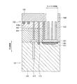
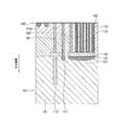
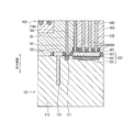
- the solid-state image sensor according to the second embodiment differs from the first embodiment in the configuration of the capacitor 120 and the configuration of the equivalent circuit.
- the description of the parts common to the first embodiment may be omitted.
- the capacitor 120 includes a first capacitor section 121 and a second capacitor section 122.
- the first capacitor unit 121 is a capacitor formed in a first capacitor region preset on the first semiconductor substrate 101.
- the first capacitor region is set at a position including the floating diffusion 111 of the first semiconductor substrate 101.
- the first capacitor portion 121 has a first electrode 131, a first dielectric film 141, and a second electrode 151.
- the first dielectric film 141 is formed in a portion of the first electrode 131 that overlaps with the second electrode 151. That is, the first electrode 131 is a portion that does not overlap with the first dielectric film 141 and the second electrode 151 when viewed from the stacking direction (vertical direction in FIG. 11) in which the first semiconductor substrate 101 and the second semiconductor substrate 102 are laminated. have. That is, a part of the first electrode 131 includes the floating diffusion 111.
- the configuration of the equivalent circuit is a configuration that does not include the switch transistor 115. Therefore, although not shown, the floating diffusion 111 is formed at a point connecting the drain electrode of the transfer transistor 112, the source electrode of the reset transistor 113, the capacitor 120, and the gate electrode of the amplification transistor 114.
- the FD side wiring electrode 161 and the third electrode 132 can be formed at the same time, so that the number of steps required for manufacturing can be reduced. It becomes possible to provide a solid-state image sensor. Further, in the configuration of the second embodiment, since the switch transistor 115 is not provided, it is possible to provide a solid-state image sensor capable of simplifying the structure.
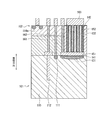
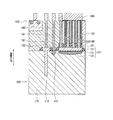
- the solid-state image sensor according to the third embodiment differs from the first embodiment in the configuration of the first semiconductor substrate 101 and the configuration of the capacitor 120.
- the description of the parts common to the first embodiment may be omitted.
- the first semiconductor substrate 101 includes a mounting electrode 170 laminated on a surface (upper surface in FIG. 12) opposite to the surface on which the light of the photodiode 110 is incident.
- the mounting electrode 170 is formed by using, for example, a polycrystalline silicon film.
- the capacitor 120 has a PD side electrode 130, a dielectric film 140, and an anti-PD side electrode 150.
- the PD side electrode 130 is formed by the third electrode 132.
- the third electrode 132 is a columnar electrode whose one end (lower end in FIG. 12) is connected to the mounting electrode 170.
- the dielectric film 140 is formed by the second dielectric film 142.
- the second dielectric film 142 covers a portion of the third electrode 132 other than the portion connected to the mounting electrode 170.
- the anti-PD side electrode 150 is formed by the fourth electrode 152.
- the fourth electrode 152 is an electrode facing the third electrode 132 with the second dielectric film 142 interposed therebetween.
- the FD side wiring electrode 161 and the third electrode 132 can be formed at the same time, so that the number of steps required for manufacturing can be reduced. It becomes possible to provide a solid-state image sensor. Further, in the configuration of the third embodiment, since the number of electrodes forming the capacitor 120 is smaller than that of the first embodiment and the second embodiment, the solid-state imaging device capable of simplifying the structure can be simplified. Can be provided. In addition to this, it becomes possible to provide a solid-state image sensor capable of reducing the number of steps required for manufacturing.
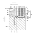
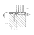
- the solid-state image sensor according to the fourth embodiment is different from the first embodiment in that the semiconductor substrate does not include the second semiconductor substrate but includes only the first semiconductor substrate 101.
- the description of the parts common to the first embodiment may be omitted.
- all of the third electrodes 132 forming the PD side electrode 130 are formed inside the first semiconductor substrate 101. Further, all of the second dielectric film 142 forming the dielectric film 140 is formed inside the first semiconductor substrate 101. Further, all of the FD side wiring electrodes 161 are formed inside the first semiconductor substrate 101. Further, in the fourth embodiment, the fifth electrode 163 is formed on the surface (upper surface in FIG. 13) opposite to the photodiode 110 side of the first semiconductor substrate 101.
- the FD side wiring electrode 161 and the third electrode 132 can be formed at the same time, so that the number of steps required for manufacturing can be reduced. It becomes possible to provide a solid-state image sensor. Further, in the configuration of the fourth embodiment, since the semiconductor substrate is configured by including only the first semiconductor substrate 101, it is possible to provide a solid-state image sensor capable of increasing the variation of the configuration. Become.
- the solid-state image sensor according to the fifth embodiment differs from the first embodiment in the configuration of the capacitor 120 and the configuration of the second semiconductor substrate 102.
- the description of the parts common to the first embodiment may be omitted.
- the capacitor 120 includes a first capacitor section 121 and a second capacitor section 122.
- the first capacitor unit 121 is a capacitor formed in a first capacitor region preset on the first semiconductor substrate 101.
- the first capacitor region is set at a position different from the position where the floating diffusion 111 of the first semiconductor substrate 101 is arranged.
- the first capacitor portion 121 has a first electrode 131, a first dielectric film 141, and a second electrode 151.
- the first electrode 131 is an electrode arranged on a surface opposite to the surface on which the light of the photodiode 110 in the first capacitor region is incident.
- the first electrode 131 and the floating diffusion 111 are formed so as to be separated from each other.
- the first dielectric film 141 is laminated on the first electrode 131.
- the second electrode 151 is laminated on the first dielectric film 141.
- the second capacitor section 122 is a capacitor arranged on the surface of the first capacitor section 121 opposite to the photodiode 110 side.
- the second capacitor portion 122 has a third electrode 132, a second dielectric film 142, and a fourth electrode 152.
- the third electrode 132 is a columnar electrode that forms the PD side electrode 130 and one end (lower end in FIG. 14) is connected to the second electrode 151. Further, a part of the lower side surface of the third electrode 132 is in contact with the intercapacitor insulating film 180 described later.
- the second dielectric film 142 forms the dielectric film 140 and covers a preset portion of the third electrode 132 including the other end (the upper end in FIG. 14).
- the fourth electrode 152 is an electrode that forms the anti-PD side electrode 150 and faces the third electrode 132 with the second dielectric film 142 sandwiched between them.
- the second semiconductor substrate 102 includes an intercapacitor insulating film 180, a first sidewall insulating film 181 and a second sidewall insulating film 182.
- the intercapacitor insulating film 180 is formed between the second electrode 151 and the second dielectric film 142.
- the intercapacitor insulating film 180 is formed by using a material different from that of the second dielectric film 142.
- a material for forming the intercapacitor insulating film 180 for example, an oxide film or a nitride film can be used.
- the oxide film or nitride film forming the intercapacitor insulating film 180 is used, for example, as a single layer.
- the intercapacitor insulating film 180 is formed by using a single-layer oxide film on the premise that the second dielectric film 142 is formed by using a material other than the oxide film. The case will be described.
- the preset portion of the third electrode 132 covered by the second dielectric film 142 is the portion of the third electrode 132 excluding a part (the portion inserted into the intercapacitor insulating film 180).
- the first sidewall insulating film 181 is formed on the side surface of the second electrode 151, and is formed by using the same material as the intercapacitor insulating film 180. Therefore, in the fifth embodiment, a case where the first sidewall insulating film 181 is formed by using a single-layer oxide film will be described as an example.
- the first sidewall insulating film 181 may be formed by using a nitride film. In this case, the first sidewall insulating film 181 is formed by using, for example, a single-layer nitride film.
- the second sidewall insulating film 182 is formed on the side surface of the transfer transistor 112, and is formed by using the same material as the intercapacitor insulating film 180. Therefore, in the fifth embodiment, a case where the second sidewall insulating film 182 is formed by using a single-layer oxide film will be described as an example.
- the second sidewall insulating film 182 may be formed by using a nitride film. In this case, the second sidewall insulating film 182 is formed by using, for example, a single-layer nitride film.
- a manufacturing method for manufacturing the solid-state image sensor of the fifth embodiment will be described with reference to FIGS. 14 and 22 with reference to FIGS. 15 to 22.
- a photodiode 110, a floating diffusion 111, and a transfer transistor 112 are formed on a first semiconductor substrate 101 formed of silicon.
- the N + region is formed by ion-implanting phosphorus or arsenic into the capacitor region, which is a preset region, in the first semiconductor substrate 101 by using an ion implantation method.
- the gate oxide film of the transfer transistor 112 is formed.
- the first dielectric film 141 laminated in the N + region is formed on the upper surface of the N + region by the silicon oxide film formed by the plasma CVD method.
- the gate electrode of the transfer transistor 112 is formed.
- the first dielectric is formed by a polycrystalline silicon film formed on the surface of the first dielectric film 141 opposite to the surface facing the N + region (the upper surface in FIG. 15) by the thermal CVD method.
- the second electrode 151 laminated on the film 141 is formed.
- an insulating forming film 183 that later becomes an intercapacitor insulating film 180, a first sidewall insulating film 181 and a second sidewall insulating film 182 is deposited on the transfer transistor 112 and the capacitor region.
- the resist 164 is formed in the capacitor region of the insulation forming film 183.
- the insulating forming film 183 is etched to form the intercapacitor insulating film 180, the first sidewall insulating film 181 and the second sidewall insulating film 182 as shown in FIG. At this time, since the resist 164 is formed in the capacitor region, the intercapacitor insulating film 180 is deposited on the second electrode 151.
- the method for manufacturing a solid-state image sensor includes a step of forming an intercapacitor insulating film 180 between the second electrode 151 and the second dielectric film 142. Further, in the step of forming the intercapacitor insulating film 180, the intercapacitor insulating film 180 is formed by using a material different from that of the second dielectric film 142.
- the method for manufacturing the solid-state imaging device includes a step of forming the first sidewall insulating film 181 formed on the side surface of the second electrode 151. Further, in the step of forming the first sidewall insulating film 181, the first sidewall insulating film 181 is formed using the same material as the intercapacitor insulating film 180. In addition to this, in the step of forming the first sidewall insulating film 181, the first sidewall insulating film 181 is formed by using an oxide film or a nitride film.
- the method for manufacturing a solid-state image pickup device includes a step of forming a second sidewall insulating film 182 formed on the side surface of the transfer transistor 112. Further, in the step of forming the second sidewall insulating film 182, the second sidewall insulating film 182 is formed by using the same material as the intercapacitor insulating film 180. In addition to this, in the step of forming the second sidewall insulating film 182, the second sidewall insulating film 182 is formed by using an oxide film or a nitride film.
- the interlayer insulating film 103 is formed by the silicon oxide film formed by the plasma CVD method.
- the second semiconductor substrate 102 formed by using the epitaxial film is laminated on the surface of the interlayer insulating film 103 opposite to the surface facing the first semiconductor substrate 101 (the upper surface in FIG. 18).
- the source / drain region 114a of the amplification transistor 114 is formed in the pixel transistor region set at a position different from the capacitor region.
- a second contact hole is connected to the floating diffusion 111 from a surface of the second semiconductor substrate 102 opposite to the surface facing the interlayer insulating film 103 (the upper surface in FIG. 18). 162 is opened.
- the first contact hole 160 that penetrates the interlayer insulating film 103 and the intercapacitor insulating film 180 and connects to the second electrode 151 is opened.
- the FD side wiring electrode 161 and the third electrode 132 are formed at the same time. Further, in the step of forming the third electrode 132, a part of the third electrode 132 including one end is inserted into the intercapacitor insulating film 180 formed in the step of forming the intercapacitor insulating film 180. , The third electrode 132 is formed.
- 164 is formed into a film.
- a plasma etching method is used to remove the portion of the interlayer insulating film 103 corresponding to the capacitor region to expose the third electrode 132.
- the resist 164 is removed.
- a selective etching condition is set in which the etching rate for the intercapacitor insulating film 180 is slower than the etching rate for the interlayer insulating film 103.
- the interlayer insulating film 103 formed on the capacitor region is etched, and the etching on the intercapacitor insulating film 180 is suppressed.
- the method for manufacturing a solid-state imaging device includes a step of forming the second capacitor portion 122 and a step of forming a second dielectric film 142 covering a preset portion including the other end portion of the third electrode 132. .. Further, in the step of forming the second dielectric film 142, a portion of the third electrode 132 excluding a part is covered with the second dielectric film 142 as a preset portion.
- a fourth electrode 152 is formed by using a refractory metal at a position facing the third electrode with the second dielectric film 142 sandwiched between them by using a sputtering method.
- the second capacitor portion 122 is formed.
- a polycrystalline silicon film is formed on the surface of the second semiconductor substrate 102 opposite to the interlayer insulating film 103 by using the thermal CVD method to form a pixel transistor region.
- one end of the third electrode 132 and a part of the lower side surface come into contact with the intercapacitor insulating film 180. Therefore, as compared with the configurations of the first to fourth embodiments, as shown in FIG. 19, the third electrode 132 when a part of the interlayer insulating film 103 is removed to expose the third electrode 132. It is possible to increase the contact area between the capacitor and the insulating film 180 between the capacitors. As a result, it is possible to prevent the third electrode 132 from collapsing as compared with the configurations of the first to fourth embodiments.
- the third electrode 132 (conductive plug) is exposed in the step of forming the second capacitor portion 122, in the configurations of the first to fourth embodiments, only the bottom portion of the third electrode 132 is the second electrode. Since it is in contact with the ground contact area, the ground contact area becomes small. Therefore, the third electrode 132 collapses due to the penetration of the cleaning liquid used when removing the interlayer insulating film 103 in the capacitor region. On the other hand, if the shape of the third electrode 132 is made a low columnar shape and the height of the third electrode 132 is lowered so that the third electrode 132 does not fall down, the area of the second capacitor portion 122 is reduced, which is desirable. It becomes difficult to obtain the capacity of.
- the shape of the third electrode 132 can be made into a high columnar shape without making it a low columnar shape, and the area of the second capacitor portion 122 can be prevented from being reduced to increase the capacitance. It becomes possible to provide a solid-state image pickup device capable of the above. Further, in the configuration of the fifth embodiment, one end of the third electrode 132 is attached to the intercapacitor insulating film 180 formed in the step of forming the intercapacitor insulating film 180 in the step of forming the third electrode 132. The third electrode 132 is formed with a part including the portion inserted. This makes it possible to provide a method for manufacturing a solid-state image sensor, which can prevent the area of the second capacitor portion 122 from being reduced and increase the capacitance.
- the solid-state image sensor according to the sixth embodiment has a different configuration of the intercapacitor insulating film 180 from the fifth embodiment.
- the description of the parts common to the fifth embodiment may be omitted.
- a plurality of openings 180a are formed on the surface of the intercapacitor insulating film 180 that opposes the second dielectric film 142 (the upper surface in FIG. 23).
- Each of the plurality of openings 180a has an opening area as seen from the length direction of the third electrode 132 (vertical direction in FIG. 23), which is a preset portion of the third electrode 132 covered by the second dielectric film 142.
- the third electrode 132 is formed in a shape smaller than the cross-sectional area seen from the length direction. Therefore, the portion of the third electrode 132 that is arranged inside the opening 180a has a cross-sectional area seen from the length direction of the third electrode 132 as compared with the portion covered by the second dielectric film 142 of the third electrode 132. Is small.
- a manufacturing method for manufacturing the solid-state image sensor of the sixth embodiment will be described with reference to FIG. 23 with reference to FIG. 24. The description of the same process as the manufacturing method for manufacturing the solid-state image sensor of the fifth embodiment will be omitted.
- the solid-state imaging device is manufactured by forming a plurality of openings 180a on the surface of the intercapacitor insulating film 180 that opposes the second dielectric film 142, as shown in FIG. 24, in the step of forming the intercapacitor insulating film 180. Form.
- the opening area seen from the length direction of the third electrode 132 is the cross-sectional area of the portion of the third electrode 132 set in advance as seen from the length direction of the third electrode 132. It is formed so as to be smaller than.
- a part of the interlayer insulating film 103 is removed to expose the third electrode 132 as compared with the configuration of the fifth embodiment. It is possible to increase the contact area between the third electrode 132 and the intercapacitor insulating film 180. This makes it possible to provide a solid-state image sensor capable of suppressing the third electrode 132 from collapsing as compared with the configuration of the fifth embodiment. Further, in the configuration of the sixth embodiment, in the step of forming the intercapacitor insulating film 180, the opening 180a is formed on the surface of the intercapacitor insulating film 180 that opposes the second dielectric film 142. This makes it possible to provide a method for manufacturing a solid-state image sensor, which can prevent the third electrode 132 from collapsing as compared with the configuration of the fifth embodiment.
- the solid-state image sensor according to the seventh embodiment has a second semiconductor substrate configuration different from that of the fifth embodiment.
- the description of the parts common to the fifth embodiment may be omitted.
- the function of the intercapacitor insulating film 180, the function of the first sidewall insulating film 181 and the second sidewall insulation are formed in the region where the second semiconductor substrate 102 is formed later.
- An integrated insulating film 184 having the function of the film 182 is formed.
- a manufacturing method for manufacturing the solid-state image sensor of the seventh embodiment will be described with reference to FIG. 25 with reference to FIG. 26. The description of the same process as the manufacturing method for manufacturing the solid-state image sensor of the fifth embodiment will be omitted.
- an insulation forming film 183 which will later become an integrated insulating film 184, is deposited on the transfer transistor 112 and the capacitor region. After that, as shown in FIG. 25, the third electrode 132 is formed, and the insulating forming film 183 functions as the integrated insulating film 184.
- the insulating forming film 183 is etched to form the intercapacitor insulating film 180, the first sidewall insulating film 181 and the second sidewall. It is possible to reduce the number of steps for forming the insulating film 182. This makes it possible to provide a solid-state image sensor capable of simplifying the manufacturing process.
- the insulating forming film 183 is etched to form the intercapacitor insulating film 180, the first sidewall insulating film 181 and the second. It is possible to reduce the number of steps for forming the sidewall insulating film 182. This makes it possible to provide a method for manufacturing a solid-state image sensor that can simplify the manufacturing process.
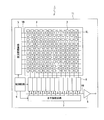
- the solid-state image sensor of the present technology can have, for example, the configuration shown in FIG. 27.
- the solid-state image sensor 1 shown in FIG. 27 is a CMOS image sensor. Further, the solid-state image sensor 1 has a pixel region 4 as an image pickup area on the semiconductor substrate 100. Further, a peripheral circuit unit (5, 6, 7, 8, 9) including, for example, a vertical drive circuit 5, a column selection circuit 6, a horizontal drive circuit 7, an output circuit 8, and a control circuit 9 in the peripheral region of the pixel region 4.
- a peripheral circuit unit (5, 6, 7, 8, 9) including, for example, a vertical drive circuit 5, a column selection circuit 6, a horizontal drive circuit 7, an output circuit 8, and a control circuit 9 in the peripheral region of the pixel region 4.
- the pixel region 4 has, for example, a plurality of unit pixels 3 (corresponding to a photodiode 110) arranged two-dimensionally in a matrix.
- a pixel drive line VD (specifically, a line selection line and a reset control line) is wired for each pixel row, and a vertical signal line VL is wired for each pixel column.
- the pixel drive line VD transmits a drive signal for reading a signal from the pixel.
- One end of the pixel drive line VD is connected to the output end corresponding to each line of the vertical drive circuit 5.
- the vertical drive circuit 5 is composed of a shift register, an address decoder, and the like.
- the vertical drive circuit 5 drives each unit pixel 3 in the pixel region 4, for example, in units of rows.
- the signal output from each unit pixel 3 of the pixel row selectively scanned by the vertical drive circuit 5 is supplied to the column selection circuit 6 through each of the vertical signal lines VL.
- the column selection circuit 6 is composed of an amplifier, a horizontal selection switch, and the like provided for each vertical signal line VL.
- the horizontal drive circuit 7 is composed of a shift register, an address decoder, and the like.
- the horizontal drive circuit 7 drives each horizontal selection switch of the column selection circuit 6 in order while scanning.
- the signals of each pixel transmitted through each of the vertical signal lines VL are sequentially output to the horizontal signal line VH and transmitted to the outside of the semiconductor substrate 100 through the horizontal signal line VH.
- the circuit portion including the vertical drive circuit 5, the column selection circuit 6, the horizontal drive circuit 7, and the horizontal signal line VH may be formed on the semiconductor substrate 100, or may be arranged on the external control IC. You may. Further, those circuit portions may be formed on another substrate connected by a cable or the like.
- the control circuit 9 receives a clock given from the outside of the semiconductor substrate 100, data for instructing an operation mode, and the like, and outputs data such as internal information of the solid-state image sensor 1. Further, the control circuit 9 has a timing generator that generates various timing signals, and based on the various timing signals generated by the timing generator, the vertical drive circuit 5, the column selection circuit 6, the horizontal drive circuit 7, etc. Controls the drive of peripheral circuits.
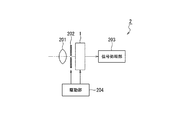
- FIG. 28 shows a schematic configuration of an electronic device 2 (camera) as a second application example.
- the electronic device 2 is, for example, a video camera capable of capturing a still image or a moving image, and drives a solid-state image sensor 1, an optical system (optical lens) 201, a shutter device 202, a solid-state image sensor 1 and a shutter device 202. It has a drive unit 204 and a signal processing unit 203.
- the optical system 201 guides the image light (incident light) from the subject to the pixel region 4 of the solid-state image sensor 1.
- the optical system 201 may be composed of a plurality of optical lenses.
- the shutter device 202 controls the light irradiation period and the light blocking period of the solid-state image sensor 1.
- the drive unit 204 controls the transfer operation of the solid-state image sensor 1 and the shutter operation of the shutter device 202.
- the signal processing unit 203 performs various signal processing on the signal output from the solid-state image sensor 1.
- the video signal after signal processing is stored in a storage medium such as a memory, or is output to a monitor or the like.
- the technology according to the present disclosure can be applied to various products.
- the technology according to the present disclosure is realized as a device mounted on a moving body of any kind such as an automobile, an electric vehicle, a hybrid electric vehicle, a motorcycle, a bicycle, a personal mobility, an airplane, a drone, a ship, and a robot. You may.
- FIG. 29 is a block diagram showing a schematic configuration example of a vehicle control system, which is an example of a mobile control system to which the technology according to the present disclosure can be applied.
- the vehicle control system 12000 includes a plurality of electronic control units connected via the communication network 12001.
- the vehicle control system 12000 includes a drive system control unit 12010, a body system control unit 12020, an outside information detection unit 12030, an in-vehicle information detection unit 12040, and an integrated control unit 12050.
- a microcomputer 12051, an audio image output unit 12052, and an in-vehicle network I / F (Interface) 12053 are shown as a functional configuration of the integrated control unit 12050.
- the drive system control unit 12010 controls the operation of the device related to the drive system of the vehicle according to various programs.
- the drive system control unit 12010 provides a driving force generator for generating the driving force of the vehicle such as an internal combustion engine or a driving motor, a driving force transmission mechanism for transmitting the driving force to the wheels, and a steering angle of the vehicle. It functions as a control device such as a steering mechanism for adjusting and a braking device for generating a braking force of a vehicle.
- the body system control unit 12020 controls the operation of various devices mounted on the vehicle body according to various programs.
- the body system control unit 12020 functions as a keyless entry system, a smart key system, a power window device, or a control device for various lamps such as headlamps, back lamps, brake lamps, blinkers or fog lamps.
- the body system control unit 12020 may be input with radio waves transmitted from a portable device that substitutes for the key or signals of various switches.
- the body system control unit 12020 receives inputs of these radio waves or signals and controls a vehicle door lock device, a power window device, a lamp, and the like.
- the vehicle outside information detection unit 12030 detects information outside the vehicle equipped with the vehicle control system 12000.
- the image pickup unit 12031 is connected to the vehicle exterior information detection unit 12030.
- the vehicle outside information detection unit 12030 causes the image pickup unit 12031 to capture an image of the outside of the vehicle and receives the captured image.
- the vehicle exterior information detection unit 12030 may perform object detection processing or distance detection processing such as a person, a vehicle, an obstacle, a sign, or characters on the road surface based on the received image.
- the image pickup unit 12031 is an optical sensor that receives light and outputs an electric signal according to the amount of the light received.
- the imaging unit 12031 can output an electric signal as an image or can output it as distance measurement information. Further, the light received by the imaging unit 12031 may be visible light or invisible light such as infrared light.
- the in-vehicle information detection unit 12040 detects the in-vehicle information.
- a driver state detection unit 12041 that detects the driver's state is connected to the in-vehicle information detection unit 12040.
- the driver state detection unit 12041 includes, for example, a camera that images the driver, and the in-vehicle information detection unit 12040 determines the degree of fatigue or concentration of the driver based on the detection information input from the driver state detection unit 12041. It may be calculated, or it may be determined whether the driver is dozing.
- the microcomputer 12051 calculates the control target value of the driving force generator, the steering mechanism, or the braking device based on the information inside and outside the vehicle acquired by the vehicle exterior information detection unit 12030 or the vehicle interior information detection unit 12040, and the drive system control unit.
- a control command can be output to 12010.
- the microcomputer 12051 realizes ADAS (Advanced Driver Assistance System) functions including vehicle collision avoidance or impact mitigation, follow-up driving based on inter-vehicle distance, vehicle speed maintenance driving, vehicle collision warning, vehicle lane deviation warning, and the like. It is possible to perform cooperative control for the purpose of.
- ADAS Advanced Driver Assistance System
- the microcomputer 12051 controls the driving force generating device, the steering mechanism, the braking device, and the like based on the information around the vehicle acquired by the outside information detection unit 12030 or the inside information detection unit 12040, so that the driver can control the driver. It is possible to perform coordinated control for the purpose of automatic driving that runs autonomously without depending on the operation.
- the microcomputer 12051 can output a control command to the body system control unit 12030 based on the information outside the vehicle acquired by the vehicle exterior information detection unit 12030.
- the microcomputer 12051 controls the headlamps according to the position of the preceding vehicle or the oncoming vehicle detected by the external information detection unit 12030, and performs cooperative control for the purpose of antiglare such as switching the high beam to the low beam. It can be carried out.
- the audio image output unit 12052 transmits the output signal of at least one of the audio and the image to the output device capable of visually or audibly notifying the passenger or the outside of the vehicle of the information.
- an audio speaker 12061, a display unit 12062, and an instrument panel 12063 are exemplified as output devices.
- the display unit 12062 may include, for example, at least one of an onboard display and a heads-up display.
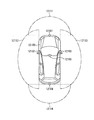
- FIG. 30 is a diagram showing an example of the installation position of the imaging unit 12031.
- the imaging units 12101, 12102, 12103, 12104, and 12105 are included.
- the imaging units 12101, 12102, 12103, 12104, 12105 are provided at positions such as, for example, the front nose, side mirrors, rear bumpers, back doors, and the upper part of the windshield in the vehicle interior of the vehicle 12100.
- the imaging unit 12101 provided on the front nose and the imaging unit 12105 provided on the upper part of the windshield in the vehicle interior mainly acquire an image in front of the vehicle 12100.
- the imaging units 12102 and 12103 provided in the side mirrors mainly acquire images of the side of the vehicle 12100.
- the imaging unit 12104 provided on the rear bumper or the back door mainly acquires an image of the rear of the vehicle 12100.
- the imaging unit 12105 provided on the upper part of the windshield in the vehicle interior is mainly used for detecting a preceding vehicle, a pedestrian, an obstacle, a traffic light, a traffic sign, a lane, or the like.
- FIG. 30 shows an example of the photographing range of the imaging units 12101 to 12104.
- the imaging range 12111 indicates the imaging range of the imaging unit 12101 provided on the front nose
- the imaging ranges 12112 and 12113 indicate the imaging ranges of the imaging units 12102 and 12103 provided on the side mirrors, respectively
- the imaging range 12114 indicates the imaging range of the imaging units 12102 and 12103.
- the imaging range of the imaging unit 12104 provided on the rear bumper or the back door is shown. For example, by superimposing the image data captured by the imaging units 12101 to 12104, a bird's-eye view image of the vehicle 12100 as viewed from above can be obtained.
- At least one of the imaging units 12101 to 12104 may have a function of acquiring distance information.
- at least one of the image pickup units 12101 to 12104 may be a stereo camera composed of a plurality of image pickup elements, or may be an image pickup element having pixels for phase difference detection.
- the microcomputer 12051 has a distance to each three-dimensional object within the imaging range 12111 to 12114 based on the distance information obtained from the imaging units 12101 to 12104, and a temporal change of this distance (relative velocity with respect to the vehicle 12100).
- a predetermined speed for example, 0 km / h or more.
- the microcomputer 12051 can set an inter-vehicle distance to be secured in front of the preceding vehicle in advance, and can perform automatic braking control (including follow-up stop control), automatic acceleration control (including follow-up start control), and the like. In this way, it is possible to perform cooperative control for the purpose of automatic driving or the like in which the vehicle travels autonomously without depending on the operation of the driver.
- the microcomputer 12051 converts three-dimensional object data related to a three-dimensional object into two-wheeled vehicles, ordinary vehicles, large vehicles, pedestrians, utility poles, and other three-dimensional objects based on the distance information obtained from the imaging units 12101 to 12104. It can be classified and extracted and used for automatic avoidance of obstacles. For example, the microcomputer 12051 distinguishes obstacles around the vehicle 12100 into obstacles that can be seen by the driver of the vehicle 12100 and obstacles that are difficult to see. Then, the microcomputer 12051 determines the collision risk indicating the risk of collision with each obstacle, and when the collision risk is equal to or higher than the set value and there is a possibility of collision, the microcomputer 12051 via the audio speaker 12061 or the display unit 12062. By outputting an alarm to the driver and performing forced deceleration and avoidance steering via the drive system control unit 12010, driving support for collision avoidance can be provided.
- At least one of the imaging units 12101 to 12104 may be an infrared camera that detects infrared rays.
- the microcomputer 12051 can recognize a pedestrian by determining whether or not a pedestrian is present in the captured image of the imaging units 12101 to 12104.
- pedestrian recognition includes, for example, a procedure for extracting feature points in an image captured by an imaging unit 12101 to 12104 as an infrared camera, and pattern matching processing for a series of feature points indicating the outline of an object to determine whether or not the pedestrian is a pedestrian. It is done by the procedure to determine.
- the audio image output unit 12052 When the microcomputer 12051 determines that a pedestrian is present in the captured images of the imaging units 12101 to 12104 and recognizes the pedestrian, the audio image output unit 12052 outputs a square contour line for emphasizing the recognized pedestrian.
- the display unit 12062 is controlled so as to superimpose and display. Further, the audio image output unit 12052 may control the display unit 12062 so as to display an icon or the like indicating a pedestrian at a desired position.
- the above is an example of a vehicle control system to which the technology according to the present disclosure can be applied.
- the technique according to the present disclosure can be applied to the imaging unit 12031 and the like among the configurations described above.
- the solid-state image sensor of FIGS. 1 to 4 and 11 to 14 can be applied to the image pickup unit 12031.
- the technology according to the present disclosure can be applied to various products.
- the techniques according to the present disclosure may be applied to endoscopic surgery systems.
- FIG. 31 is a diagram showing an example of a schematic configuration of an endoscopic surgery system to which the technique according to the present disclosure (the present technique) can be applied.
- FIG. 31 illustrates how the surgeon (doctor) 11131 is performing surgery on patient 11132 on patient bed 11133 using the endoscopic surgery system 11000.
- the endoscopic surgery system 11000 includes an endoscope 11100, other surgical tools 11110 such as an abdominal tube 11111 and an energy treatment tool 11112, and a support arm device 11120 that supports the endoscope 11100.
- a cart 11200 equipped with various devices for endoscopic surgery.
- the endoscope 11100 is composed of a lens barrel 11101 in which a region having a predetermined length from the tip is inserted into the body cavity of the patient 11132, and a camera head 11102 connected to the base end of the lens barrel 11101.
- the endoscope 11100 configured as a so-called rigid mirror having a rigid barrel 11101 is illustrated, but the endoscope 11100 may be configured as a so-called flexible mirror having a flexible barrel. Good.
- An opening in which an objective lens is fitted is provided at the tip of the lens barrel 11101.
- a light source device 11203 is connected to the endoscope 11100, and the light generated by the light source device 11203 is guided to the tip of the lens barrel by a light guide extending inside the lens barrel 11101 to be an objective. It is irradiated toward the observation target in the body cavity of the patient 11132 through the lens.
- the endoscope 11100 may be a direct endoscope, a perspective mirror, or a side endoscope.
- An optical system and an image sensor are provided inside the camera head 11102, and the reflected light (observation light) from the observation target is focused on the image sensor by the optical system.
- the observation light is photoelectrically converted by the image sensor, and an electric signal corresponding to the observation light, that is, an image signal corresponding to the observation image is generated.
- the image signal is transmitted as RAW data to the camera control unit (CCU: Camera Control Unit) 11201.
- CCU Camera Control Unit
- the CCU11201 is composed of a CPU (Central Processing Unit), a GPU (Graphics Processing Unit), and the like, and comprehensively controls the operations of the endoscope 11100 and the display device 11202. Further, the CCU 11201 receives an image signal from the camera head 11102, and performs various image processes on the image signal for displaying an image based on the image signal, such as development processing (demosaic processing).
- a CPU Central Processing Unit
- GPU Graphics Processing Unit
- the display device 11202 displays an image based on the image signal processed by the CCU 11201 under the control of the CCU 11201.
- the light source device 11203 is composed of, for example, a light source such as an LED (Light Emitting Diode), and supplies irradiation light to the endoscope 11100 when photographing an operating part or the like.
- a light source such as an LED (Light Emitting Diode)
- LED Light Emitting Diode
- the input device 11204 is an input interface for the endoscopic surgery system 11000.
- the user can input various information and input instructions to the endoscopic surgery system 11000 via the input device 11204.
- the user inputs an instruction to change the imaging conditions (type of irradiation light, magnification, focal length, etc.) by the endoscope 11100.
- the treatment tool control device 11205 controls the drive of the energy treatment tool 11112 for cauterizing, incising, sealing a blood vessel, or the like of a tissue.
- the pneumoperitoneum device 11206 uses a gas in the pneumoperitoneum tube 11111 to inflate the body cavity of the patient 11132 for the purpose of securing the field of view by the endoscope 11100 and securing the work space of the operator.
- the recorder 11207 is a device capable of recording various information related to surgery.
- the printer 11208 is a device capable of printing various information related to surgery in various formats such as text, images, and graphs.
- the light source device 11203 that supplies the irradiation light to the endoscope 11100 when photographing the surgical site can be composed of, for example, an LED, a laser light source, or a white light source composed of a combination thereof.
- a white light source is configured by combining RGB laser light sources, the output intensity and output timing of each color (each wavelength) can be controlled with high accuracy. Therefore, the light source device 11203 adjusts the white balance of the captured image. It can be carried out.
- the laser light from each of the RGB laser light sources is irradiated to the observation target in a time-divided manner, and the drive of the image sensor of the camera head 11102 is controlled in synchronization with the irradiation timing to support each of RGB. It is also possible to capture the image in a time-divided manner. According to this method, a color image can be obtained without providing a color filter on the image sensor.
- the drive of the light source device 11203 may be controlled so as to change the intensity of the output light at predetermined time intervals.
- the drive of the image sensor of the camera head 11102 in synchronization with the timing of the change of the light intensity to acquire an image in time division and synthesizing the image, so-called high dynamic without blackout and overexposure. Range images can be generated.
- the light source device 11203 may be configured to be able to supply light in a predetermined wavelength band corresponding to special light observation.
- special light observation for example, by utilizing the wavelength dependence of light absorption in body tissue to irradiate light in a narrow band as compared with the irradiation light (that is, white light) in normal observation, the mucosal surface layer.
- a so-called narrow band imaging is performed in which a predetermined tissue such as a blood vessel is photographed with high contrast.
- fluorescence observation in which an image is obtained by fluorescence generated by irradiating with excitation light may be performed.
- the body tissue is irradiated with excitation light to observe the fluorescence from the body tissue (autofluorescence observation), or a reagent such as indocyanine green (ICG) is locally injected into the body tissue and the body tissue is injected. It is possible to obtain a fluorescence image by irradiating excitation light corresponding to the fluorescence wavelength of the reagent.
- the light source device 11203 may be configured to be capable of supplying narrow band light and / or excitation light corresponding to such special light observation.
- FIG. 32 is a block diagram showing an example of the functional configuration of the camera head 11102 and CCU11201 shown in FIG. 31.
- the camera head 11102 includes a lens unit 11401, an imaging unit 11402, a driving unit 11403, a communication unit 11404, and a camera head control unit 11405.
- CCU11201 has a communication unit 11411, an image processing unit 11412, and a control unit 11413.
- the camera head 11102 and CCU11201 are communicably connected to each other by a transmission cable 11400.
- the lens unit 11401 is an optical system provided at a connection portion with the lens barrel 11101.
- the observation light taken in from the tip of the lens barrel 11101 is guided to the camera head 11102 and incident on the lens unit 11401.
- the lens unit 11401 is configured by combining a plurality of lenses including a zoom lens and a focus lens.
- the image pickup unit 11402 is composed of an image pickup element.
- the image sensor constituting the image pickup unit 11402 may be one (so-called single plate type) or a plurality (so-called multi-plate type).
- each image pickup element may generate an image signal corresponding to each of RGB, and a color image may be obtained by synthesizing them.
- the image pickup unit 11402 may be configured to have a pair of image pickup elements for acquiring image signals for the right eye and the left eye corresponding to 3D (Dimensional) display, respectively.
- the 3D display enables the operator 11131 to more accurately grasp the depth of the biological tissue in the surgical site.
- a plurality of lens units 11401 may be provided corresponding to each image pickup element.
- the imaging unit 11402 does not necessarily have to be provided on the camera head 11102.
- the image pickup unit 11402 may be provided inside the lens barrel 11101 immediately after the objective lens.
- the drive unit 11403 is composed of an actuator, and the zoom lens and the focus lens of the lens unit 11401 are moved by a predetermined distance along the optical axis under the control of the camera head control unit 11405. As a result, the magnification and focus of the image captured by the imaging unit 11402 can be adjusted as appropriate.
- the communication unit 11404 is composed of a communication device for transmitting and receiving various information to and from the CCU11201.
- the communication unit 11404 transmits the image signal obtained from the image pickup unit 11402 as RAW data to the CCU 11201 via the transmission cable 11400.
- the communication unit 11404 receives a control signal for controlling the drive of the camera head 11102 from the CCU 11201 and supplies the control signal to the camera head control unit 11405.
- the control signal includes, for example, information to specify the frame rate of the captured image, information to specify the exposure value at the time of imaging, and / or information to specify the magnification and focus of the captured image. Contains information about the condition.
- the imaging conditions such as the frame rate, exposure value, magnification, and focus may be appropriately specified by the user, or may be automatically set by the control unit 11413 of the CCU 11201 based on the acquired image signal. Good. In the latter case, the so-called AE (Auto Exposure) function, AF (Auto Focus) function, and AWB (Auto White Balance) function are mounted on the endoscope 11100.
- AE Auto Exposure
- AF Automatic Focus
- AWB Auto White Balance
- the camera head control unit 11405 controls the drive of the camera head 11102 based on the control signal from the CCU 11201 received via the communication unit 11404.
- the communication unit 11411 is composed of a communication device for transmitting and receiving various information to and from the camera head 11102.
- the communication unit 11411 receives an image signal transmitted from the camera head 11102 via the transmission cable 11400.
- the communication unit 11411 transmits a control signal for controlling the drive of the camera head 11102 to the camera head 11102.
- Image signals and control signals can be transmitted by telecommunications, optical communication, or the like.
- the image processing unit 11412 performs various image processing on the image signal which is the RAW data transmitted from the camera head 11102.
- the control unit 11413 performs various controls related to the imaging of the surgical site and the like by the endoscope 11100 and the display of the captured image obtained by the imaging of the surgical site and the like. For example, the control unit 11413 generates a control signal for controlling the drive of the camera head 11102.
- control unit 11413 causes the display device 11202 to display an image captured by the surgical unit or the like based on the image signal processed by the image processing unit 11412.
- the control unit 11413 may recognize various objects in the captured image by using various image recognition techniques. For example, the control unit 11413 detects the shape and color of the edge of an object included in the captured image to remove surgical tools such as forceps, a specific biological part, bleeding, and mist when using the energy treatment tool 11112. Can be recognized.
- the control unit 11413 may superimpose and display various surgical support information on the image of the surgical unit by using the recognition result. By superimposing and displaying the operation support information and presenting it to the operator 11131, it is possible to reduce the burden on the operator 11131 and to allow the operator 11131 to proceed with the operation reliably.
- the transmission cable 11400 that connects the camera head 11102 and CCU11201 is an electric signal cable that supports electrical signal communication, an optical fiber that supports optical communication, or a composite cable thereof.
- the communication was performed by wire using the transmission cable 11400, but the communication between the camera head 11102 and the CCU11201 may be performed wirelessly.
- the above is an example of an endoscopic surgery system to which the technology according to the present disclosure can be applied.
- the technique according to the present disclosure can be applied to, for example, the endoscope 11100, the camera head 11102 (imaging unit 11402), and the like) among the configurations described above.
- the technique according to the present disclosure By applying the technique according to the present disclosure to the endoscope 11100 and the imaging unit 11402, it becomes possible to improve the manufacturing efficiency.
- the semiconductor device of the present disclosure does not need to include all of the components described in the above-described embodiments and the like, and conversely, other components may be provided.
- the effects described in the present specification are merely examples and are not limited, and other effects may be obtained.
- the present technology can have the following configurations.
- a semiconductor substrate including a photodiode that photoelectrically converts incident light and a floating diffusion that transfers signal charges accumulated in the photodiode.
- a capacitor having a PD-side electrode arranged on a surface of the photodiode opposite to the surface on which the light is incident, and an anti-PD-side electrode facing the PD-side electrode with a dielectric film interposed therebetween.
- An amplification transistor that reads out and amplifies the signal charge transferred to the floating diffusion as an electric signal, and The FD side wiring electrode for connecting the floating diffusion and the amplification transistor is provided.
- the semiconductor substrate includes a first semiconductor substrate on which a pixel circuit including the photodiode and the floating diffusion is arranged, and a second semiconductor substrate laminated on a surface of the first semiconductor substrate opposite to the photodiode side.
- the capacitors include a first capacitor portion formed in a first capacitor region preset on the first semiconductor substrate, a second capacitor portion arranged on a surface of the first capacitor portion opposite to the photodiode side, and a second capacitor portion.
- the first capacitor portion includes a first electrode arranged on a surface of the first capacitor region opposite to the photodiode side, a first dielectric film laminated on the first electrode, and a laminate on the first dielectric film.
- the second capacitor portion has a columnar third electrode that forms the PD side electrode and one end of which is connected to the second electrode and is formed inside the first contact hole, and the dielectric film.
- a second dielectric film covering a portion of the third electrode other than the portion connected to the second electrode and the anti-PD side electrode are formed, and the second dielectric film is sandwiched between the second dielectric film. It has a fourth electrode facing the electrode and The solid-state imaging device according to (2) above, wherein the first electrode and the floating diffusion are formed so as to be separated from each other. (4) The solid-state image sensor according to (3) above, wherein the second electrode is formed by using a polycrystalline silicon film. (5) The solid-state imaging device according to (3) or (4), wherein at least one of the third electrode and the fourth electrode is formed of a refractory metal.
- the solid-state imaging device according to any one of (3) to (5) above, wherein the second dielectric film is formed by using a ferroelectric film.
- the first capacitor portion includes a first electrode arranged on a surface of the first capacitor region opposite to the photodiode side, a first dielectric film laminated on the first electrode, and a laminate on the first dielectric film.
- the second capacitor portion has a columnar third electrode that forms the PD side electrode and one end of which is connected to the second electrode and is formed inside the first contact hole, and the dielectric film.
- a second dielectric film covering a portion of the third electrode other than the portion connected to the second electrode and the anti-PD side electrode are formed, and the second dielectric film is sandwiched between the second dielectric film.
- the solid-state image sensor according to (2) above has a fourth electrode facing the electrode and The solid-state image sensor according to (2) above, wherein a part of the first electrode includes the floating diffusion.
- the semiconductor substrate includes a first semiconductor substrate on which a pixel circuit including the photodiode and the floating diffusion is arranged, and a second semiconductor substrate laminated on a surface of the first semiconductor substrate opposite to the photodiode side. And, including The first semiconductor substrate includes a mounting electrode laminated on a surface of the photodiode opposite to the surface on which the light is incident. The PD-side electrode is formed, and one end of the electrode is connected to the above-mentioned electrode, and a columnar third electrode formed inside the first contact hole forms the dielectric film, and the first contact hole is formed.
- a second dielectric film that covers a portion other than the portion connected to the previously described electrode of the three electrodes and a fourth electrode that forms the anti-PD side electrode and faces the third electrode with the second dielectric film sandwiched between them.
- (12) The solid-state image sensor according to (11), wherein at least one of the third electrode and the fourth electrode is formed of a refractory metal.
- (13) The solid-state imaging device according to (11) or (12) above, wherein the second dielectric film is formed by using a ferroelectric film.
- the capacitor includes a first capacitor portion formed in a first capacitor region preset on the semiconductor substrate, and a second capacitor portion arranged on a surface of the first capacitor portion opposite to the photodiode side.
- the first capacitor portion includes a first electrode arranged on a surface of the first capacitor region opposite to the photodiode side, a first dielectric film laminated on the first electrode, and a laminate on the first dielectric film.
- the second capacitor portion has a columnar third electrode that forms the PD side electrode and one end of which is connected to the second electrode and is formed inside the first contact hole, and the dielectric film.
- a second dielectric film covering a portion of the third electrode other than the portion connected to the second electrode and the anti-PD side electrode are formed, and the second dielectric film is sandwiched between the second dielectric film.
- the solid-state imaging device according to (1) has a fourth electrode facing the electrode and The solid-state imaging device according to (1), wherein the first electrode and the floating diffusion are formed so as to be separated from each other.
- the capacitor includes a first capacitor portion formed in a first capacitor region preset on the semiconductor substrate, and a second capacitor portion arranged on a surface of the first capacitor portion opposite to the photodiode side.
- the first capacitor portion includes a first electrode arranged on a surface of the first capacitor region opposite to the photodiode side, a first dielectric film laminated on the first electrode, and a laminate on the first dielectric film.
- the second capacitor portion forms the PD side electrode, and one end portion is connected to the second electrode, and a columnar third electrode formed inside the first contact hole, and the dielectric film.
- the second dielectric film covering a preset portion including the other end of the third electrode and the anti-PD side electrode are formed, and the second dielectric film is sandwiched between the second dielectric film. It has a fourth electrode facing the third electrode and The first electrode and the floating diffusion are formed so as to be separated from each other.
- An intercapacitor insulating film formed between the second electrode and the second dielectric film is provided. A part of the third electrode including one end thereof is inserted into the intercapacitor insulating film.
- a transfer transistor for turning on or off the transfer of electric charge from the photodiode to the floating diffusion, and a second sidewall insulating film formed on the side surface of the transfer transistor are provided.
- the opening area seen from the length direction of the third electrode is the length direction of the preset portion of the third electrode.
- a process of forming a photodiode that photoelectrically converts incident light and a floating diffusion that transfers signal charges accumulated in the photodiode on a semiconductor substrate A step of forming a capacitor having a PD-side electrode arranged on a surface of the photodiode opposite to the surface on which the light is incident, and an anti-PD-side electrode facing the PD-side electrode with a dielectric film interposed therebetween.
- a step of forming an amplification transistor that reads out and amplifies the signal charge transferred to the floating diffusion as an electric signal is provided.
- the first contact hole that forms at least a part of the PD side electrode inside and the FD side wiring electrode that connects the floating diffusion and the amplification transistor are formed inside.
- Manufacture of a solid-state image sensor including a step of simultaneously forming a shape in the semiconductor substrate as a shape extending along the thickness direction of the semiconductor substrate and a step of simultaneously forming the FD side wiring electrode and the PD side electrode.
- Method. (26) A process of forming a photodiode that photoelectrically converts incident light and a floating diffusion that transfers signal charges accumulated in the photodiode on a semiconductor substrate.
- a step of forming an amplification transistor that reads out and amplifies the signal charge transferred to the floating diffusion as an electric signal is provided.
- a first contact hole for forming at least a part of the PD side electrode inside and a second contact hole for forming an FD side wiring electrode for connecting the floating diffusion and the amplification transistor are formed inside.
- a method for manufacturing a solid-state image sensor which comprises a step of simultaneously forming and in the semiconductor substrate as a shape extending along the thickness direction of the semiconductor substrate.
- (27) A process of forming a photodiode that photoelectrically converts incident light and a floating diffusion that transfers signal charges accumulated in the photodiode on a semiconductor substrate.
- a step of forming an amplification transistor that reads out and amplifies the signal charge transferred to the floating diffusion as an electric signal is provided.
- the PD side electrode is formed in the first contact hole that forms at least a part of the PD side electrode inside, and the FD side wiring electrode that connects the floating diffusion and the amplification transistor is formed.
- a method for manufacturing a solid-state image sensor which comprises a step of simultaneously forming the FD-side wiring electrode in a second contact hole to be formed inside.
- (28) A process of forming a photodiode that photoelectrically converts incident light and a floating diffusion that transfers signal charges accumulated in the photodiode on a semiconductor substrate.
- the step of forming the capacitor is arranged on a surface opposite to the step of forming the first capacitor portion formed in the first capacitor region set in advance on the semiconductor substrate and the photodiode side of the first capacitor portion.
- the steps of forming the first capacitor portion include a step of forming a first electrode arranged on a surface opposite to the photodiode side of the first capacitor region and a first dielectric film laminated on the first electrode.
- It includes a step of forming and a step of forming a second electrode laminated on the first dielectric film.
- a columnar third electrode formed inside the first contact hole while forming the PD side electrode and connecting one end to the second electrode is formed.
- a step of forming an intercapacitor insulating film between the second electrode and the second dielectric film is further included.
- a part of the third electrode including the one end is inserted into the intercapacitor insulating film.
- a method for manufacturing a solid-state image sensor in which a portion of the third electrode excluding a part of the third electrode is covered with the second dielectric film as the preset portion is provided.
- the step of forming the first sidewall insulating film formed on the side surface of the second electrode is further included.
- the solid-state image sensor according to (28) or (29) above which forms the first sidewall insulating film using the same material as the intercapacitor insulating film.
- Method. (31) The method for manufacturing a solid-state image sensor according to (30), wherein in the step of forming the first sidewall insulating film, the first sidewall insulating film is formed by using an oxide film or a nitride film. (32) Further including a step of forming a transfer transistor for turning on or off the transfer of electric charge from the photodiode to the floating diffusion, and a step of forming a second sidewall insulating film formed on the side surface of the transfer transistor.
- Method of manufacturing the element (33) The method for manufacturing a solid-state image sensor according to (32), wherein the second sidewall insulating film is formed by using an oxide film or a nitride film in the step of forming the second sidewall insulating film. (34) In the step of forming the intercapacitor insulating film, the opening area of the intercapacitor insulating film on the surface facing the second dielectric film as seen from the length direction of the third electrode is formed among the third electrodes. The method for manufacturing a solid-state image sensor according to any one of (28) to (33), wherein an opening smaller than the cross-sectional area of the preset portion as viewed from the length direction is formed.
- 1 Solid-state imaging element, 2 ... Electronic equipment, 3 ... Unit pixel, 4 ... Pixel region, 5 ... Vertical drive circuit, 6 ... Column selection circuit, 7 ... Horizontal drive circuit, 8 ... Output circuit, 9 ... Control circuit, 100 ... Semiconductor substrate, 101 ... First semiconductor substrate, 102 ... Second semiconductor substrate, 103 ... Intermediate insulating film, 110 ... Photodiode, 111 ... Floating diffusion, 112 ... Transfer electrode, 113 ... Reset transistor, 114 ... Amplification transistor, 114a ... Source / drain region of amplification transistor 114, 115 ... Switch transistor, 116 ... Selective transistor, 120 ... Capsule, 121 ... First capacitor section, 122 ...
- Second capacitor section 130 ... PD side electrode, 131 ... First electrode, 131a ... N + region, 132 ... third electrode, 140 ... dielectric film, 141 ... first dielectric film, 142 ... second dielectric film, 150 ... anti-PD side electrode, 151 ... second electrode, 152 ... fourth electrode, 160 ... 1st contact hole, 161 ... FD side wiring electrode, 162 ... 2nd contact hole, 163 ... 5th electrode, 164 ... resist, 170 ... mounting electrode, 180 ... inter-semiconductor insulating film, 180a ... opening, 181 ... 1st sidewall insulating film, 182 ... 2nd sidewall insulating film, 183 ...
- Stomach device 11207 ... Recorder, 11208 ... Printer, 11400 ... Transmission cable, 11401 ... Lens unit, 11402 ... Imaging unit, 11403 ... Drive unit, 11404 ... Communication unit, 11405 ... Camera head control unit, 11411 ... Communication unit, 11412 ... Image processing unit, 11413 ... Control unit, 12000 ... Vehicle control system, 12001 ... Communication network, 12010 Drive system control unit ..., 12020 ... Body system control unit, 12030 ... External information detection unit, 12031 (1210) 1 to 12105) ... Imaging unit, 12040 ... Vehicle information detection unit, 12041 ... Driver status detection unit, 12050 ... Integrated control unit, 12051 ... Microcomputer, 12052 ... Audio image output unit, 12053 ...
- In-vehicle network I / F 12061 ... Audio speaker, 12062 ... Display unit, 12063 ... Instrument panel, 12100 ... Vehicle, 12111-12114 ... Imaging range, VD ... Pixel drive line, VL ... Vertical signal line, VH ... Horizontal signal line
Landscapes
- Solid State Image Pick-Up Elements (AREA)
Abstract
Description
そこで、例えば、特許文献1に開示されている技術のように、フォトダイオード等を形成した第1半導体基板と、画素トランジスタを形成した第2半導体基板とを積層した構成において、第2半導体基板にトレンチキャパシタを形成する技術がある。特許文献1に開示されている技術であれば、面積を減少させることなくキャパシタの面積を確保することが可能となる。
本技術の一態様に係る固体撮像素子の製造方法は、半導体基板に、入射した光を光電変換するフォトダイオードと、フォトダイオードに蓄積された信号電荷が転送されるフローティングディフュージョンと、を形成する工程を備える。さらに、フォトダイオードの光が入射する面と反対の面に配置したPD側電極と、PD側電極と誘電膜を間に挟んで対向する反PD側電極と、を有するキャパシタを形成する工程を備える。これに加え、フローティングディフュージョンに転送された信号電荷を電気信号として読み出して増幅する増幅トランジスタを形成する工程を備える。そして、キャパシタを形成する工程は、PD側電極の少なくとも一部を内部に形成する第1コンタクトホールとフローティングディフュージョンと増幅トランジスタとを接続するFD側配線電極を内部に形成する第2コンタクトホールとを半導体基板内に半導体基板の厚さ方向に沿って延びる形状として同時に形成する工程を含む。
本技術の一態様に係る固体撮像素子の製造方法は、半導体基板に、入射した光を光電変換するフォトダイオードと、フォトダイオードに蓄積された信号電荷が転送されるフローティングディフュージョンと、を形成する工程を備える。さらに、フォトダイオードの光が入射する面と反対の面に配置したPD側電極と、PD側電極と誘電膜を間に挟んで対向する反PD側電極と、を有するキャパシタを形成する工程を備える。これに加え、フローティングディフュージョンに転送された信号電荷を電気信号として読み出して増幅する増幅トランジスタを形成する工程を備える。そして、PD側電極の少なくとも一部を内部に形成する第1コンタクトホールへのPD側電極の形成と、フローティングディフュージョンと増幅トランジスタとを接続するFD側配線電極を内部に形成する第2コンタクトホールへのFD側配線電極の形成と、を同時に行う工程を含む。
<固体撮像素子の全体構成>
第1実施形態に係る固体撮像素子は、例えば、裏面照射型の固体撮像素子である。
図1から図4に示すように、固体撮像素子は、第1半導体基板101と、第2半導体基板102とを含む半導体基板を備える。
第2半導体基板102は、第1半導体基板101のフォトダイオード110側とは反対の面(図4中では、上側の面)に積層した基板である。なお、図2には、隣接した画素の第2半導体基板102NPを図示している。
第2半導体基板102の第1半導体基板101と対向する面と反対の面(図4中では、上側の面)には、第5電極163が形成されている。
第5電極163は、例えば、多結晶シリコン膜を用いて形成されている。また、第5電極163は、固体撮像素子の等価回路を構成する配線を形成している。
フォトダイオード110の一端は、接地されている。フォトダイオード110の他端は、転送トランジスタ112のソース電極に接続されている。
また、フローティングディフュージョン111は、フォトダイオード110から転送トランジスタ112を介して転送されてくる電荷を蓄積し、電圧に変換する。すなわち、フローティングディフュージョン111は、フォトダイオード110に蓄積された信号電荷が転送される。
また、転送トランジスタ112は、図外のタイミング制御部からゲート電極に供給される駆動信号に従って、フォトダイオード110からフローティングディフュージョン111への電荷の転送をオン又はオフする。
また、スイッチトランジスタ115は、図外の切り替え制御部からゲート電極に供給される切り替え信号に従って、キャパシタ120からフローティングディフュージョン111への電荷の転送をオン又はオフする。
PD側電極130は、フォトダイオード110の光が入射する面と反対の面に配置した電極である。
反PD側電極150は、PD側電極130と誘電膜140を間に挟んで対向する電極である。
第1キャパシタ部121は、第1半導体基板101に予め設定した第1キャパシタ領域に形成したキャパシタである。
第1キャパシタ領域は、第1半導体基板101のフローティングディフュージョン111を配置した位置と異なる位置に設定されている。
第1電極131は、第1キャパシタ領域のフォトダイオード110の光が入射する面と反対の面に配置した電極である。第1電極131とフローティングディフュージョン111とは、互いに離間して形成されている。
また、第1電極131は、第1キャパシタ領域にイオン注入したリン又はヒ素を用いて形成されている。
また、第1誘電膜141は、酸化シリコン膜を用いて形成されている。
第2電極151は、第1誘電膜141に積層されている。
また、第2電極151は、多結晶シリコン膜を用いて形成されている。
第2キャパシタ部122は、第3電極132と、第2誘電膜142と、第4電極152とを有する。
また、第3電極132は、タングステン、窒化チタン、コバルト、ルテニウム等の高融点金属を用いて形成されている。なお、高融点金属とは、例えば、鉄の融点以上の融点を有する金属である。
さらに、第3電極132は、第1コンタクトホール160の内部に形成されている。
したがって、PD側電極130を形成する第3電極132は、第1コンタクトホール160の内部に形成されている。すなわち、PD側電極130の少なくとも一部は、第1コンタクトホール160の内部に形成されているとともに、半導体基板内に、半導体基板の厚さ方向に沿って延びる形状に形成されている。
また、第1コンタクトホール160の一部は、第1半導体基板101の内部に形成されており、第1コンタクトホール160の残りの部分は、第2半導体基板102の内部に形成されている。
したがって、第2誘電膜142の一部は、第1半導体基板101の内部に形成されており、第2誘電膜142の残りの部分は、第2半導体基板102の内部に形成されている。
また、第2誘電膜142は、強誘電体膜を用いて形成されている。
強誘電体膜としては、酸化膜と窒化膜の積層膜、酸化膜と五酸化タンタル膜の積層膜、窒化膜と五酸化タンタル膜の積層膜、酸化膜と窒化膜と五酸化タンタル膜の積層膜、ハフニウム及びハフニウム合金材料、BSTやPZT等を用いることが可能である。
また、第4電極152は、第3電極132と同様、タングステン、窒化チタン、コバルト、ルテニウム等の高融点金属を用いて形成されている。
FD側配線電極161は、第2コンタクトホール162の内部に形成されている。
また、FD側配線電極161は、第3電極132と同様、タングステン、窒化チタン、コバルト、ルテニウム等の高融点金属を用いて形成されている。
したがって、FD側配線電極161の一部は、第1半導体基板101の内部に形成されており、FD側配線電極161の残りの部分は、第2半導体基板102の内部に形成されている。また、FD側配線電極161は、半導体基板内に、半導体基板の厚さ方向に沿って延びる形状に形成されている。
また、第1コンタクトホール160の一端と第2コンタクトホール162の一端(共に、図4では、上側の開口端)は、共に半導体基板(第1半導体基板101、第2半導体基板102)の、フォトダイオード110側とは反対の面に位置している。
また、リセットトランジスタ113は、タイミング制御部からゲート電極に供給される駆動信号に従って、フローティングディフュージョン111に蓄積されている電荷の排出をオン又はオフする。
また、増幅トランジスタ114は、リセットトランジスタ113によってリセットされたフローティングディフュージョン111の電位を、リセットレベルとして読み出す。さらに、増幅トランジスタ114は、転送トランジスタ112によって信号電荷が転送された、フローティングディフュージョン111に蓄積されている信号電荷に応じた電圧を増幅する。すなわち、増幅トランジスタ114は、フローティングディフュージョン111に転送された信号電荷を、電気信号として読み出して増幅する。
増幅トランジスタ114により増幅された電圧(電圧信号)は、選択トランジスタ116を介して垂直信号線VLに出力される。
ここで、フローティングディフュージョン111と増幅トランジスタ114とは、FD側配線電極161により接続されている。
また、選択トランジスタ116は、タイミング制御部からゲート電極に供給される駆動信号SELに従って、増幅トランジスタ114から垂直信号線VLへの電圧信号の出力を、オン又はオフする。
これにより、選択トランジスタ116は、ゲート電極に選択制御信号が与えられることで導通状態になり、垂直走査回路(図示せず)による垂直走査に同期して単位画素を選択する。なお、選択トランジスタ116の構成は、増幅トランジスタ114のソース電極とソース線との間に接続する構成としてもよい。
図1から図4を参照しつつ、図5から図10を用いて、第1実施形態の固体撮像素子を製造する製造方法を説明する。
固体撮像素子の製造方法では、まず、図5に示すように、シリコンを用いて形成した第1半導体基板101に、フォトダイオード110、フローティングディフュージョン111、転送トランジスタ112を形成する。すなわち、固体撮像素子の製造方法は、半導体基板に、フォトダイオード110と、フローティングディフュージョン111を形成する工程を備える。
さらに、第1半導体基板101のうち、予め設定した領域であるキャパシタ領域に対し、イオン注入法を用いて、リン又はヒ素をイオン注入する。これにより、後に第1電極131となるN+領域131aを形成する。N+領域131aは、後工程で行う熱処理により、第1電極131となる。
次に、転送トランジスタ112のゲート酸化膜を形成する。これに加え、N+領域131aの上面(図5中では、上側の面)に、プラズマCVD法を用いて成膜した酸化シリコン膜により、N+領域131aに積層した第1誘電膜141を形成する。
次に、図6に示すように、層間絶縁膜103の第1半導体基板101と対向する面と反対の面(図6中では、上側の面)に、エピタキシャル膜を用いて形成した第2半導体基板102を積層させる。
さらに、スパッタ法を用いて、第2コンタクトホール162の内部と、第1コンタクトホール160の内部に高融点金属を成膜することで、FD側配線電極161と第3電極132を同時に形成する。
また、固体撮像素子の製造方法では、キャパシタを形成する工程が、第1コンタクトホール160と第2コンタクトホール120とを半導体基板内に半導体基板の厚さ方向に沿って延びる形状として同時に形成する工程を含む。これに加え、固体撮像素子の製造方法では、キャパシタを形成する工程が、FD側配線電極161とPD側電極130とを同時に形成する工程を含む。
次に、熱CVD法を用いて、図10に示すように、第2半導体基板102の層間絶縁膜103と対向する面と反対の面に多結晶シリコン膜を成膜することで、画素トランジスタ領域とキャパシタ領域に、配線となる第5電極163を形成する。すなわち、固体撮像素子の製造方法は、増幅トランジスタ114を形成する工程を備える。
さらに、第1実施形態の構成であれば、キャパシタ120の構成が、第1キャパシタ部121と第2キャパシタ部122を積層した構成である。このため、固体撮像素子の微細化によりキャパシタ120を配置する面積が減少する構成であっても、キャパシタ120に要求される容量を得ることが容易となる。
スイッチトランジスタ115のゲートをオフにする場合、フローティングディフュージョン111がキャパシタ120と切り離されるため、容量が低下する。また、フローティングディフュージョン111は、容量が小さいため、少ない電子で電位が大きく下がり、感度の高い信号が出力される。ただし、信号の電子が多いときには、フローティングディフュージョン111から電子が溢れてしまうので、フォトダイオード110に入射した光の量に応じた本来の信号を得ることが困難である。一方、スイッチトランジスタ115のゲートをオンにした場合には、フローティングディフュージョン111がキャパシタ120と接続されるため、容量が増加する。容量が増加すると、多くの電子を受け止めることが可能となる代わりに、感度が低くなる。
上述したように、スイッチトランジスタ115のゲートを切り替えることで、高感度の動作モードで電荷を読み出した画像と、低感度の動作モードで電荷を読み出した画像とを画像合成することが可能となる。これにより、固体撮像素子のダイナミックレンジを拡大することが可能となる。
第1実施形態では、第3電極132及び第4電極152を、高融点金属を用いて形成したが、これに限定するものではなく、第3電極132又は第4電極152の一方のみを、高融点金属を用いて形成してもよい。
第1実施形態では、キャパシタを形成する工程が、第1コンタクトホール160と第2コンタクトホール120とを同時に形成する工程と、FD側配線電極161とPD側電極130とを同時に形成する工程を含む。しかしながら、これに限定するものではない。すなわち、キャパシタを形成する工程が、第1コンタクトホール160と第2コンタクトホール120とを同時に形成する工程のみを含んでもよい。同様に、キャパシタを形成する工程が、FD側配線電極161とPD側電極130とを同時に形成する工程のみを含んでもよい。
第2実施形態に係る固体撮像素子は、図11に示すように、キャパシタ120の構成と、等価回路の構成が、第1実施形態と相違する。以下の説明では、第1実施形態との共通する部分の説明を省略する場合がある。
第1キャパシタ部121は、第1半導体基板101に予め設定した第1キャパシタ領域に形成したキャパシタである。
第1キャパシタ領域は、第1半導体基板101のフローティングディフュージョン111を含む位置に設定されている。
第1誘電膜141は、第1電極131のうち、第2電極151と重なる部分に形成されている。すなわち、第1電極131は、第1半導体基板101と第2半導体基板102を積層した積層方向(図11では、上下方向)から見て、第1誘電膜141及び第2電極151と重ならない部分を有している。すなわち、第1電極131の一部が、フローティングディフュージョン111を含む。
さらに、第2実施形態の構成であれば、スイッチトランジスタ115を備えていないため、構造を簡略化することが可能な固体撮像素子を提供することが可能となる。
第3実施形態に係る固体撮像素子は、図12に示すように、第1半導体基板101の構成と、キャパシタ120の構成が、第1実施形態と相違する。以下の説明では、第1実施形態との共通する部分の説明を省略する場合がある。
載置電極170は、例えば、多結晶シリコン膜を用いて形成されている。
PD側電極130は、第3電極132によって形成されている。
第3電極132は、一方の端部(図12では、下側の端部)が載置電極170と接続する柱状の電極である。
誘電膜140は、第2誘電膜142によって形成されている。
第2誘電膜142は、第3電極132の載置電極170と接続する部分以外を覆う。
反PD側電極150は、第4電極152によって形成されている。
第4電極152は、第2誘電膜142を間に挟んで第3電極132と対向する電極である。
さらに、第3実施形態の構成であれば、第1実施形態及び第2実施形態と比較して、キャパシタ120を形成する電極の数が少ないため、構造を簡略化することが可能な固体撮像素子を提供することが可能となる。これに加え、製造に要する工程数を削減することが可能な固体撮像素子を提供することが可能となる。
第4実施形態に係る固体撮像素子は、図13に示すように、半導体基板が、第2半導体基板を含まず、第1半導体基板101のみを含む構成で、第1実施形態と相違する。以下の説明では、第1実施形態との共通する部分の説明を省略する場合がある。
さらに、第4実施形態では、第5電極163は、第1半導体基板101のフォトダイオード110側とは反対の面(図13中では、上側の面)に形成されている。
さらに、第4実施形態の構成であれば、第1半導体基板101のみを含んで半導体基板を構成しているため、構成のバリエーションを増加させることが可能な固体撮像素子を提供することが可能となる。
第5実施形態に係る固体撮像素子は、図14に示すように、キャパシタ120の構成と、第2半導体基板102の構成が、第1実施形態と相違する。以下の説明では、第1実施形態との共通する部分の説明を省略する場合がある。
第1キャパシタ部121は、第1半導体基板101に予め設定した第1キャパシタ領域に形成したキャパシタである。
第1キャパシタ領域は、第1半導体基板101のフローティングディフュージョン111を配置した位置と異なる位置に設定されている。
第1電極131は、第1キャパシタ領域のフォトダイオード110の光が入射する面と反対の面に配置した電極である。第1電極131とフローティングディフュージョン111とは、互いに離間して形成されている。
第2電極151は、第1誘電膜141に積層されている。
第2キャパシタ部122は、第3電極132と、第2誘電膜142と、第4電極152とを有する。
また、第3電極132のうち、下側の一部の側面は、後述するキャパシタ間絶縁膜180と接触している。
第4電極152は、反PD側電極150を形成し、且つ第2誘電膜142を間に挟んで第3電極132と対向する電極である。
キャパシタ間絶縁膜180は、第2電極151と第2誘電膜142との間に形成されている。
キャパシタ間絶縁膜180を形成する材料としては、例えば、酸化膜又は窒化膜を用いることが可能である。また、キャパシタ間絶縁膜180を形成する酸化膜又は窒化膜は、例えば、単層で用いる。
第5実施形態では、一例として、第2誘電膜142が、酸化膜以外の材料を用いて形成されている構成を前提とし、キャパシタ間絶縁膜180を、単層の酸化膜を用いて形成した場合について説明する。
したがって、第3電極132のうち、第2誘電膜142が覆う予め設定した部分は、第3電極132のうち、一部(キャパシタ間絶縁膜180に挿入されている部分)を除く部分である。
したがって、第5実施形態では、一例として、第1サイドウォール絶縁膜181を、単層の酸化膜を用いて形成した場合について説明する。
なお、第1サイドウォール絶縁膜181は、窒化膜を用いて形成してもよい。この場合、第1サイドウォール絶縁膜181は、例えば、単層の窒化膜を用いて形成する。
したがって、第5実施形態では、一例として、第2サイドウォール絶縁膜182を、単層の酸化膜を用いて形成した場合について説明する。
なお、第2サイドウォール絶縁膜182は、窒化膜を用いて形成してもよい。この場合、第2サイドウォール絶縁膜182は、例えば、単層の窒化膜を用いて形成する。
図14を参照しつつ、図15から図22を用いて、第5実施形態の固体撮像素子を製造する製造方法を説明する。
固体撮像素子の製造方法では、まず、図15に示すように、シリコンを用いて形成した第1半導体基板101に、フォトダイオード110、フローティングディフュージョン111、転送トランジスタ112を形成する。
次に、転送トランジスタ112のゲート酸化膜を形成する。これに加え、N+領域の上面に、プラズマCVD法を用いて成膜した酸化シリコン膜により、N+領域に積層した第1誘電膜141を形成する。
そして、図16に示すように、転送トランジスタ112とキャパシタ領域に、後にキャパシタ間絶縁膜180、第1サイドウォール絶縁膜181、第2サイドウォール絶縁膜182となる絶縁形成膜183を堆積させる。その後、絶縁形成膜183のうち、キャパシタ領域にレジスト164を形成する。
また、キャパシタ間絶縁膜180を形成する工程では、第2誘電膜142と異なる材料を用いてキャパシタ間絶縁膜180を形成する。
また、第1サイドウォール絶縁膜181を形成する工程では、キャパシタ間絶縁膜180と同じ材料を用いて第1サイドウォール絶縁膜181を形成する。
これに加え、第1サイドウォール絶縁膜181を形成する工程では、酸化膜又は窒化膜を用いて、第1サイドウォール絶縁膜181を形成する。
また、第2サイドウォール絶縁膜182を形成する工程では、キャパシタ間絶縁膜180と同じ材料を用いて、第2サイドウォール絶縁膜182を形成する。
これに加え、第2サイドウォール絶縁膜182を形成する工程では、酸化膜又は窒化膜を用いて、第2サイドウォール絶縁膜182を形成する。
これに加え、層間絶縁膜103の第1半導体基板101と対向する面と反対の面(図18中では、上側の面)に、エピタキシャル膜を用いて形成した第2半導体基板102を積層させる。
さらに、スパッタ法を用いて、第2コンタクトホール162の内部と、第1コンタクトホール160の内部に高融点金属を成膜することで、FD側配線電極161と第3電極132を同時に形成する。
また、第3電極132を形成する工程では、キャパシタ間絶縁膜180を形成する工程で形成したキャパシタ間絶縁膜180に、第3電極132のうち一方の端部を含む一部を挿入した状態で、第3電極132を形成する。
このとき、層間絶縁膜103に対するエッチング速度よりもキャパシタ間絶縁膜180に対するエッチング速度が遅くなる選択エッチング条件を設定する。これにより、キャパシタ領域の上に形成した層間絶縁膜103にエッチングを行い、キャパシタ間絶縁膜180に対するエッチングを抑制する。
すなわち、固体撮像素子の製造方法は、第2キャパシタ部122を形成する工程が、第3電極132のうち他方の端部を含む予め設定した部分を覆う第2誘電膜142を形成する工程を含む。また、第2誘電膜142を形成する工程では、予め設定した部分として第3電極132のうち一部を除く部分を第2誘電膜142で覆う。
次に、熱CVD法を用いて、図22に示すように、第2半導体基板102の層間絶縁膜103と対向する面と反対の面に多結晶シリコン膜を成膜することで、画素トランジスタ領域とキャパシタ領域に、配線となる第5電極163を形成する。
具体的に、第2キャパシタ部122を形成する工程において、第3電極132(導電プラグ)を露出させると、第1~第4実施形態の構成では、第3電極132の底部のみが第2電極と接触しているため、接地面積が小さくなる。そのため、キャパシタ領域の層間絶縁膜103を除去する際に用いる洗浄液の染み込みにより、第3電極132が倒れることとなる。これに対し、第3電極132が倒れないように、第3電極132の形状を低い円柱状として、第3電極132の高さを低くすると、第2キャパシタ部122の面積が減少するため、所望の容量を得ることが困難となる。
その結果、第3電極132の形状を、低い円柱状とすること無く、高い円柱状とすることが可能となり、第2キャパシタ部122の面積が減少することを防止して、容量を増加させることが可能な固体撮像素子を提供することが可能となる。
さらに、第5実施形態の構成であれば、第3電極132を形成する工程で、キャパシタ間絶縁膜180を形成する工程で形成したキャパシタ間絶縁膜180に、第3電極132のうち一方の端部を含む一部を挿入した状態で、第3電極132を形成する。これにより、第2キャパシタ部122の面積が減少することを防止して、容量を増加させることが可能な、固体撮像素子の製造方法を提供することが可能となる。
第6実施形態に係る固体撮像素子は、キャパシタ間絶縁膜180の構成が、第5実施形態と相違する。以下の説明では、第5実施形態との共通する部分の説明を省略する場合がある。
具体的には、図23に示すように、キャパシタ間絶縁膜180のうち第2誘電膜142と対抗する面(図23では、上側の面)に、複数の開口部180aが形成されている。
したがって、第3電極132のうち開口部180aの内部に配置されている部分は、第3電極132の第2誘電膜142が覆う部分よりも、第3電極132の長さ方向から見た断面積が小さい。
図23を参照しつつ、図24を用いて、第6実施形態の固体撮像素子を製造する製造方法を説明する。なお、第5実施形態の固体撮像素子を製造する製造方法と同様の工程については、説明を省略する。
固体撮像素子の製造方法は、キャパシタ間絶縁膜180を形成する工程で、図24に示すように、キャパシタ間絶縁膜180のうち第2誘電膜142と対抗する面に、複数の開口部180aを形成する。その際、複数の開口部180aは、第3電極132の長さ方向から見た開口面積が、第3電極132のうち予め設定した部分の、第3電極132の長さ方向から見た断面積よりも小さくなるように形成する。
さらに、第6実施形態の構成であれば、キャパシタ間絶縁膜180を形成する工程で、キャパシタ間絶縁膜180のうち第2誘電膜142と対抗する面に、開口部180aを形成する。これにより、第5実施形態の構成と比較して、第3電極132が倒れることを抑制することが可能な、固体撮像素子の製造方法を提供することが可能となる。
第7実施形態に係る固体撮像素子は、第2半導体基板の構成が、第5実施形態と相違する。以下の説明では、第5実施形態との共通する部分の説明を省略する場合がある。
具体的には、図25に示すように、後に第2半導体基板102が形成される領域に、キャパシタ間絶縁膜180の機能と、第1サイドウォール絶縁膜181の機能と、第2サイドウォール絶縁膜182の機能とを有する統合絶縁膜184が形成されている。
図25を参照しつつ、図26を用いて、第7実施形態の固体撮像素子を製造する製造方法を説明する。なお、第5実施形態の固体撮像素子を製造する製造方法と同様の工程については、説明を省略する。
固体撮像素子の製造方法は、図26に示すように、転送トランジスタ112とキャパシタ領域に、後に統合絶縁膜184となる絶縁形成膜183を堆積させる。その後、図25に示すように、第3電極132を形成し、絶縁形成膜183を統合絶縁膜184として機能させる。
さらに、第7実施形態の構成であれば、第5実施形態の構成と比較して、絶縁形成膜183をエッチングして、キャパシタ間絶縁膜180と、第1サイドウォール絶縁膜181と、第2サイドウォール絶縁膜182を形成する工程を削減することが可能となる。これにより、製造工程を簡略化することが可能な、固体撮像素子の製造方法を提供することが可能となる。
本技術の固体撮像素子は、例えば、図27中に示す構成とすることが可能である。
画素領域4は、例えば、行列状に2次元配置された複数の単位画素3(フォトダイオード110に相当)を有する。単位画素3には、例えば、画素行ごとに画素駆動線VD(具体的には、行選択線及びリセット制御線)が配線され、画素列ごとに垂直信号線VLが配線されている。画素駆動線VDは、画素からの信号読み出しのための駆動信号を伝送する。画素駆動線VDの一端は、垂直駆動回路5の各行に対応した出力端に接続されている。
カラム選択回路6は、垂直信号線VLごとに設けられたアンプや水平選択スイッチ等によって構成されている。
垂直駆動回路5、カラム選択回路6、水平駆動回路7及び水平信号線VHを含む回路部分は、半導体基板100上に形成されていてもよく、又は、外部制御ICに配設されたものであってもよい。また、それらの回路部分は、ケーブル等により接続された他の基板に形成されていてもよい。
本技術の固体撮像素子は、デジタルスチルカメラやビデオカメラ等のカメラシステムや、撮像機能を有する携帯電話等、撮像機能を備えたあらゆるタイプの電子機器に適用することが可能である。例えば、図28中に、第2適用例としての電子機器2(カメラ)の概略構成を示す。
シャッタ装置202は、固体撮像素子1への光照射期間及び遮光期間を制御する。
信号処理部203は、固体撮像素子1から出力された信号に対し、各種の信号処理を行う。信号処理後の映像信号は、メモリ等の記憶媒体に記憶されるか、あるいは、モニタ等に出力される。
本開示に係る技術(本技術)は、様々な製品へ応用することができる。例えば、本開示に係る技術は、自動車、電気自動車、ハイブリッド電気自動車、自動二輪車、自転車、パーソナルモビリティ、飛行機、ドローン、船舶、ロボット等のいずれかの種類の移動体に搭載される装置として実現されてもよい。
本開示に係る技術は、様々な製品へ応用することができる。例えば、本開示に係る技術は、内視鏡手術システムに適用されてもよい。
(その他の実施形態)
上記のように、本技術の実施形態を記載したが、この開示の一部をなす論述及び図面は本技術を限定するものであると理解すべきではない。この開示から当業者には様々な代替実施形態、実施例及び運用技術が明らかとなろう。
その他、上記の実施形態において説明される各構成を任意に応用した構成等、本技術はここでは記載していない様々な実施形態等を含むことは勿論である。したがって、本技術の技術的範囲は上記の説明から妥当な特許請求の範囲に係る発明特定事項によってのみ定められるものである。
また、本開示の半導体装置では、上記の実施形態等で説明した各構成要素を全て備える必要はなく、また逆に他の構成要素を備えていてもよい。
なお、本明細書中に記載された効果はあくまで例示であって限定されるものでは無く、また他の効果があってもよい。
(1)
入射した光を光電変換するフォトダイオードと、前記フォトダイオードに蓄積された信号電荷が転送されるフローティングディフュージョンと、を含む半導体基板と、
前記フォトダイオードの前記光が入射する面と反対の面に配置したPD側電極と、前記PD側電極と誘電膜を間に挟んで対向する反PD側電極と、を有するキャパシタと、
前記フローティングディフュージョンに転送された信号電荷を電気信号として読み出して増幅する増幅トランジスタと、
前記フローティングディフュージョンと前記増幅トランジスタとを接続するFD側配線電極と、を備え、
前記PD側電極の少なくとも一部と前記FD側配線電極とは、前記半導体基板内に半導体基板の厚さ方向に沿って延びる形状に形成され、
前記PD側電極の少なくとも一部を内部に形成する第1コンタクトホールの一端と前記FD側配線電極を内部に形成する第2コンタクトホールの一端は、共に前記半導体基板の前記フォトダイオード側とは反対の面に位置している固体撮像素子。
(2)
前記半導体基板は、前記フォトダイオードと、前記フローティングディフュージョンと、を備える画素回路を配置した第1半導体基板と、前記第1半導体基板の前記フォトダイオード側とは反対の面に積層した第2半導体基板と、を含み、
前記キャパシタは、前記第1半導体基板に予め設定した第1キャパシタ領域に形成した第1キャパシタ部と、前記第1キャパシタ部の前記フォトダイオード側とは反対の面に配置した第2キャパシタ部と、を含む前記(1)に記載した固体撮像素子。
(3)
前記第1キャパシタ部は、前記第1キャパシタ領域の前記フォトダイオード側とは反対の面に配置した第1電極と、前記第1電極に積層した第1誘電膜と、前記第1誘電膜に積層した第2電極と、を有し、
前記第2キャパシタ部は、前記PD側電極を形成し、且つ一方の端部が前記第2電極と接続するともに前記第1コンタクトホールの内部に形成される柱状の第3電極と、前記誘電膜を形成し、且つ前記第3電極の前記第2電極と接続する部分以外を覆う第2誘電膜と、前記反PD側電極を形成し、且つ前記第2誘電膜を間に挟んで前記第3電極と対向する第4電極と、を有し、
前記第1電極と前記フローティングディフュージョンとは、互いに離間して形成されている前記(2)に記載した固体撮像素子。
(4)
前記第2電極は、多結晶シリコン膜を用いて形成されている前記(3)に記載した固体撮像素子。
(5)
前記第3電極及び前記第4電極のうち少なくとも一方は、高融点金属を用いて形成されている前記(3)又は(4)に記載した固体撮像素子。
(6)
前記第2誘電膜は、強誘電体膜を用いて形成されている前記(3)~(5)のいずれかに記載した固体撮像素子。
(7)
前記第1キャパシタ部は、前記第1キャパシタ領域の前記フォトダイオード側とは反対の面に配置した第1電極と、前記第1電極に積層した第1誘電膜と、前記第1誘電膜に積層した第2電極と、を有し、
前記第2キャパシタ部は、前記PD側電極を形成し、且つ一方の端部が前記第2電極と接続するともに前記第1コンタクトホールの内部に形成される柱状の第3電極と、前記誘電膜を形成し、且つ前記第3電極の前記第2電極と接続する部分以外を覆う第2誘電膜と、前記反PD側電極を形成し、且つ前記第2誘電膜を間に挟んで前記第3電極と対向する第4電極と、を有し、
前記第1電極の一部は、前記フローティングディフュージョンを含む前記(2)に記載した固体撮像素子。
(8)
前記第2電極は、多結晶シリコン膜を用いて形成されている前記(7)に記載した固体撮像素子。
(9)
前記第3電極及び前記第4電極のうち少なくとも一方は、高融点金属を用いて形成されている前記(7)又は(8)に記載した固体撮像素子。
(10)
前記第2誘電膜は、強誘電体膜を用いて形成されている前記(7)~(9)のいずれかに記載した固体撮像素子。
(11)
前記半導体基板は、前記フォトダイオードと、前記フローティングディフュージョンと、を備える画素回路を配置した第1半導体基板と、前記第1半導体基板の前記フォトダイオード側とは反対の面に積層した第2半導体基板と、を含み、
前記第1半導体基板は、前記フォトダイオードの前記光が入射する面と反対の面に積層した載置電極を含み、
前記PD側電極を形成し、且つ一方の端部が前記載置電極と接続するともに前記第1コンタクトホールの内部に形成される柱状の第3電極と、前記誘電膜を形成し、且つ前記第3電極の前記載置電極と接続する部分以外を覆う第2誘電膜と、前記反PD側電極を形成し、且つ前記第2誘電膜を間に挟んで前記第3電極と対向する第4電極と、を有する前記(1)に記載した固体撮像素子。
(12)
前記第3電極及び前記第4電極のうち少なくとも一方は、高融点金属を用いて形成されている前記(11)に記載した固体撮像素子。
(13)
前記第2誘電膜は、強誘電体膜を用いて形成されている前記(11)又は(12)に記載した固体撮像素子。
(14)
前記キャパシタは、前記半導体基板に予め設定した第1キャパシタ領域に形成した第1キャパシタ部と、前記第1キャパシタ部の前記フォトダイオード側とは反対の面に配置した第2キャパシタ部と、を含み、
前記第1キャパシタ部は、前記第1キャパシタ領域の前記フォトダイオード側とは反対の面に配置した第1電極と、前記第1電極に積層した第1誘電膜と、前記第1誘電膜に積層した第2電極と、を有し、
前記第2キャパシタ部は、前記PD側電極を形成し、且つ一方の端部が前記第2電極と接続するともに前記第1コンタクトホールの内部に形成される柱状の第3電極と、前記誘電膜を形成し、且つ前記第3電極の前記第2電極と接続する部分以外を覆う第2誘電膜と、前記反PD側電極を形成し、且つ前記第2誘電膜を間に挟んで前記第3電極と対向する第4電極と、を有し、
前記第1電極と前記フローティングディフュージョンとは、互いに離間して形成されている前記(1)に記載した固体撮像素子。
(15)
前記第2電極は、多結晶シリコン膜を用いて形成されている前記(14)に記載した固体撮像素子。
(16)
前記第3電極及び前記第4電極のうち少なくとも一方は、高融点金属を用いて形成されている前記(14)又は(15)に記載した固体撮像素子。
(17)
前記第2誘電膜は、強誘電体膜を用いて形成されている前記(14)~(16)のいずれかに記載した固体撮像素子。
(18)
前記キャパシタは、前記半導体基板に予め設定した第1キャパシタ領域に形成した第1キャパシタ部と、前記第1キャパシタ部の前記フォトダイオード側とは反対の面に配置した第2キャパシタ部と、を含み、
前記第1キャパシタ部は、前記第1キャパシタ領域の前記フォトダイオード側とは反対の面に配置した第1電極と、前記第1電極に積層した第1誘電膜と、前記第1誘電膜に積層した第2電極と、を有し、
前記第2キャパシタ部は、前記PD側電極を形成し、且つ一方の端部が前記第2電極と接続するともに前記第1コンタクトホールの内部に形成される柱状の第3電極と、前記誘電膜を形成し、且つ前記第3電極のうち他方の端部を含む予め設定した部分を覆う第2誘電膜と、前記反PD側電極を形成し、且つ前記第2誘電膜を間に挟んで前記第3電極と対向する第4電極と、を有し、
前記第1電極と前記フローティングディフュージョンとは、互いに離間して形成され、
前記第2電極と前記第2誘電膜との間に形成されたキャパシタ間絶縁膜を備え、
前記キャパシタ間絶縁膜には、前記第3電極のうち前記一方の端部を含む一部が挿入され、
前記第2誘電膜が覆う前記予め設定した部分は、前記第3電極のうち前記一部を除く部分である前記(1)に記載した固体撮像素子。
(19)
前記キャパシタ間絶縁膜は、前記第2誘電膜と異なる材料を用いて形成されている前記(18)に記載した固体撮像素子。
(20)
前記第2電極の側面に形成された第1サイドウォール絶縁膜を備え、
前記第1サイドウォール絶縁膜は、前記キャパシタ間絶縁膜と同じ材料を用いて形成されている前記(18)又は(19)に記載した固体撮像素子。
(21)
前記第1サイドウォール絶縁膜は、酸化膜又は窒化膜を用いて形成されている前記(20)に記載した固体撮像素子。
(22)
前記フォトダイオードから前記フローティングディフュージョンへの電荷の転送をオン又はオフする転送トランジスタと、前記転送トランジスタの側面に形成された第2サイドウォール絶縁膜と、を備え、
前記第2サイドウォール絶縁膜は、前記キャパシタ間絶縁膜と同じ材料を用いて形成されている前記(18)~(21)のいずれかに記載した固体撮像素子。
(23)
前記第2サイドウォール絶縁膜は、酸化膜又は窒化膜を用いて形成されている前記(22)に記載した固体撮像素子。
(24)
前記キャパシタ間絶縁膜のうち前記第2誘電膜と対抗する面には、前記第3電極の長さ方向から見た開口面積が、前記第3電極のうち前記予め設定した部分の前記長さ方向から見た断面積よりも小さい開口部が形成されている前記(18)~(23)のいずれかに記載した固体撮像素子。
(25)
半導体基板に、入射した光を光電変換するフォトダイオードと、前記フォトダイオードに蓄積された信号電荷が転送されるフローティングディフュージョンと、を形成する工程と、
前記フォトダイオードの前記光が入射する面と反対の面に配置したPD側電極と、前記PD側電極と誘電膜を間に挟んで対向する反PD側電極と、を有するキャパシタを形成する工程と、
前記フローティングディフュージョンに転送された信号電荷を電気信号として読み出して増幅する増幅トランジスタを形成する工程と、を備え、
前記キャパシタを形成する工程は、前記PD側電極の少なくとも一部を内部に形成する第1コンタクトホールと前記フローティングディフュージョンと前記増幅トランジスタとを接続するFD側配線電極を内部に形成する第2コンタクトホールとを前記半導体基板内に半導体基板の厚さ方向に沿って延びる形状として同時に形成する工程と、前記FD側配線電極と前記PD側電極とを同時に形成する工程と、を含む固体撮像素子の製造方法。
(26)
半導体基板に、入射した光を光電変換するフォトダイオードと、前記フォトダイオードに蓄積された信号電荷が転送されるフローティングディフュージョンと、を形成する工程と、
前記フォトダイオードの前記光が入射する面と反対の面に配置したPD側電極と、前記PD側電極と誘電膜を間に挟んで対向する反PD側電極と、を有するキャパシタを形成する工程と、
前記フローティングディフュージョンに転送された信号電荷を電気信号として読み出して増幅する増幅トランジスタを形成する工程と、を備え、
前記キャパシタを形成する工程は、前記PD側電極の少なくとも一部を内部に形成する第1コンタクトホールと前記フローティングディフュージョンと前記増幅トランジスタとを接続するFD側配線電極を内部に形成する第2コンタクトホールとを前記半導体基板内に半導体基板の厚さ方向に沿って延びる形状として同時に形成する工程を含む固体撮像素子の製造方法。
(27)
半導体基板に、入射した光を光電変換するフォトダイオードと、前記フォトダイオードに蓄積された信号電荷が転送されるフローティングディフュージョンと、を形成する工程と、
前記フォトダイオードの前記光が入射する面と反対の面に配置したPD側電極と、前記PD側電極と誘電膜を間に挟んで対向する反PD側電極と、を有するキャパシタを形成する工程と、
前記フローティングディフュージョンに転送された信号電荷を電気信号として読み出して増幅する増幅トランジスタを形成する工程と、を備え、
前記キャパシタを形成する工程は、前記PD側電極の少なくとも一部を内部に形成する第1コンタクトホールへのPD側電極の形成と、前記フローティングディフュージョンと前記増幅トランジスタとを接続するFD側配線電極を内部に形成する第2コンタクトホールへの前記FD側配線電極の形成と、を同時に行う工程を含む固体撮像素子の製造方法。
(28)
半導体基板に、入射した光を光電変換するフォトダイオードと、前記フォトダイオードに蓄積された信号電荷が転送されるフローティングディフュージョンと、を形成する工程と、
前記フォトダイオードの前記光が入射する面と反対の面に配置したPD側電極と、前記PD側電極と誘電膜を間に挟んで対向する反PD側電極と、を有するキャパシタを形成する工程と、を備え、
前記キャパシタを形成する工程は、前記半導体基板に予め設定した第1キャパシタ領域に形成した第1キャパシタ部を形成する工程と、前記第1キャパシタ部の前記フォトダイオード側とは反対の面に配置した第2キャパシタ部を形成する工程と、を含み、
前記第1キャパシタ部を形成する工程は、前記第1キャパシタ領域の前記フォトダイオード側とは反対の面に配置した第1電極を形成する工程と、前記第1電極に積層した第1誘電膜を形成する工程と、前記第1誘電膜に積層した第2電極を形成する工程と、を含み、
前記第2キャパシタ部を形成する工程は、前記PD側電極を形成し、且つ一方の端部が前記第2電極と接続するともに前記第1コンタクトホールの内部に形成される柱状の第3電極を形成する工程と、前記誘電膜を形成し、且つ前記第3電極のうち他方の端部を含む予め設定した部分を覆う第2誘電膜を形成する工程と、前記反PD側電極を形成し、且つ前記第2誘電膜を間に挟んで前記第3電極と対向する第4電極を形成する工程と、を含み、
前記第2電極と前記第2誘電膜との間にキャパシタ間絶縁膜を形成する工程をさらに含み、
前記キャパシタ間絶縁膜を形成する工程では、前記キャパシタ間絶縁膜に前記第3電極のうち前記一方の端部を含む一部を挿入し、
前記第2誘電膜を形成する工程では、前記予め設定した部分として前記第3電極のうち前記一部を除く部分を第2誘電膜で覆う固体撮像素子の製造方法。
(29)
前記キャパシタ間絶縁膜を形成する工程では、前記第2誘電膜と異なる材料を用いて前記キャパシタ間絶縁膜を形成する前記(28)に記載した固体撮像素子の製造方法。
(30)
前記第2電極の側面に形成された第1サイドウォール絶縁膜を形成する工程をさらに含み、
前記第1サイドウォール絶縁膜を形成する工程では、前記キャパシタ間絶縁膜と同じ材料を用いて前記第1サイドウォール絶縁膜を形成する前記(28)又は(29)に記載した固体撮像素子の製造方法。
(31)
前記第1サイドウォール絶縁膜を形成する工程では、酸化膜又は窒化膜を用いて前記第1サイドウォール絶縁膜を形成する前記(30)に記載した固体撮像素子の製造方法。
(32)
前記フォトダイオードから前記フローティングディフュージョンへの電荷の転送をオン又はオフする転送トランジスタを形成する工程と、前記転送トランジスタの側面に形成された第2サイドウォール絶縁膜を形成する工程と、をさらに含み、
前記第2サイドウォール絶縁膜を形成する工程では、前記キャパシタ間絶縁膜と同じ材料を用いて前記第2サイドウォール絶縁膜を形成する前記(28)~(31)のいずれかに記載した固体撮像素子の製造方法。
(33)
前記第2サイドウォール絶縁膜を形成する工程では、酸化膜又は窒化膜を用いて前記第2サイドウォール絶縁膜を形成する前記(32)に記載した固体撮像素子の製造方法。
(34)
前記キャパシタ間絶縁膜を形成する工程では、前記キャパシタ間絶縁膜のうち前記第2誘電膜と対抗する面に、前記第3電極の長さ方向から見た開口面積が、前記第3電極のうち前記予め設定した部分の前記長さ方向から見た断面積よりも小さい開口部を形成する前記(28)~(33)のいずれかに記載した固体撮像素子の製造方法。
Claims (34)
- 入射した光を光電変換するフォトダイオードと、前記フォトダイオードに蓄積された信号電荷が転送されるフローティングディフュージョンと、を含む半導体基板と、
前記フォトダイオードの前記光が入射する面と反対の面に配置したPD側電極と、前記PD側電極と誘電膜を間に挟んで対向する反PD側電極と、を有するキャパシタと、
前記フローティングディフュージョンに転送された信号電荷を電気信号として読み出して増幅する増幅トランジスタと、
前記フローティングディフュージョンと前記増幅トランジスタとを接続するFD側配線電極と、を備え、
前記PD側電極の少なくとも一部と前記FD側配線電極とは、前記半導体基板内に半導体基板の厚さ方向に沿って延びる形状に形成され、
前記PD側電極の少なくとも一部を内部に形成する第1コンタクトホールの一端と前記FD側配線電極を内部に形成する第2コンタクトホールの一端は、共に前記半導体基板の前記フォトダイオード側とは反対の面に位置している固体撮像素子。 - 前記半導体基板は、前記フォトダイオードと、前記フローティングディフュージョンと、を備える画素回路を配置した第1半導体基板と、前記第1半導体基板の前記フォトダイオード側とは反対の面に積層した第2半導体基板と、を含み、
前記キャパシタは、前記第1半導体基板に予め設定した第1キャパシタ領域に形成した第1キャパシタ部と、前記第1キャパシタ部の前記フォトダイオード側とは反対の面に配置した第2キャパシタ部と、を含む請求項1に記載した固体撮像素子。 - 前記第1キャパシタ部は、前記第1キャパシタ領域の前記フォトダイオード側とは反対の面に配置した第1電極と、前記第1電極に積層した第1誘電膜と、前記第1誘電膜に積層した第2電極と、を有し、
前記第2キャパシタ部は、前記PD側電極を形成し、且つ一方の端部が前記第2電極と接続するともに前記第1コンタクトホールの内部に形成される柱状の第3電極と、前記誘電膜を形成し、且つ前記第3電極の前記第2電極と接続する部分以外を覆う第2誘電膜と、前記反PD側電極を形成し、且つ前記第2誘電膜を間に挟んで前記第3電極と対向する第4電極と、を有し、
前記第1電極と前記フローティングディフュージョンとは、互いに離間して形成されている請求項2に記載した固体撮像素子。 - 前記第2電極は、多結晶シリコン膜を用いて形成されている請求項3に記載した固体撮像素子。
- 前記第3電極及び前記第4電極のうち少なくとも一方は、高融点金属を用いて形成されている請求項3に記載した固体撮像素子。
- 前記第2誘電膜は、強誘電体膜を用いて形成されている請求項3に記載した固体撮像素子。
- 前記第1キャパシタ部は、前記第1キャパシタ領域の前記フォトダイオード側とは反対の面に配置した第1電極と、前記第1電極に積層した第1誘電膜と、前記第1誘電膜に積層した第2電極と、を有し、
前記第2キャパシタ部は、前記PD側電極を形成し、且つ一方の端部が前記第2電極と接続するともに前記第1コンタクトホールの内部に形成される柱状の第3電極と、前記誘電膜を形成し、且つ前記第3電極の前記第2電極と接続する部分以外を覆う第2誘電膜と、前記反PD側電極を形成し、且つ前記第2誘電膜を間に挟んで前記第3電極と対向する第4電極と、を有し、
前記第1電極の一部は、前記フローティングディフュージョンを含む請求項2に記載した固体撮像素子。 - 前記第2電極は、多結晶シリコン膜を用いて形成されている請求項7に記載した固体撮像素子。
- 前記第3電極及び前記第4電極のうち少なくとも一方は、高融点金属を用いて形成されている請求項7に記載した固体撮像素子。
- 前記第2誘電膜は、強誘電体膜を用いて形成されている請求項7に記載した固体撮像素子。
- 前記半導体基板は、前記フォトダイオードと、前記フローティングディフュージョンと、を備える画素回路を配置した第1半導体基板と、前記第1半導体基板の前記フォトダイオード側とは反対の面に積層した第2半導体基板と、を含み、
前記第1半導体基板は、前記フォトダイオードの前記光が入射する面と反対の面に積層した載置電極を含み、
前記PD側電極を形成し、且つ一方の端部が前記載置電極と接続するともに前記第1コンタクトホールの内部に形成される柱状の第3電極と、前記誘電膜を形成し、且つ前記第3電極の前記載置電極と接続する部分以外を覆う第2誘電膜と、前記反PD側電極を形成し、且つ前記第2誘電膜を間に挟んで前記第3電極と対向する第4電極と、を有する請求項1に記載した固体撮像素子。 - 前記第3電極及び前記第4電極のうち少なくとも一方は、高融点金属を用いて形成されている請求項11に記載した固体撮像素子。
- 前記第2誘電膜は、強誘電体膜を用いて形成されている請求項11に記載した固体撮像素子。
- 前記キャパシタは、前記半導体基板に予め設定した第1キャパシタ領域に形成した第1キャパシタ部と、前記第1キャパシタ部の前記フォトダイオード側とは反対の面に配置した第2キャパシタ部と、を含み、
前記第1キャパシタ部は、前記第1キャパシタ領域の前記フォトダイオード側とは反対の面に配置した第1電極と、前記第1電極に積層した第1誘電膜と、前記第1誘電膜に積層した第2電極と、を有し、
前記第2キャパシタ部は、前記PD側電極を形成し、且つ一方の端部が前記第2電極と接続するともに前記第1コンタクトホールの内部に形成される柱状の第3電極と、前記誘電膜を形成し、且つ前記第3電極の前記第2電極と接続する部分以外を覆う第2誘電膜と、前記反PD側電極を形成し、且つ前記第2誘電膜を間に挟んで前記第3電極と対向する第4電極と、を有し、
前記第1電極と前記フローティングディフュージョンとは、互いに離間して形成されている請求項1に記載した固体撮像素子。 - 前記第2電極は、多結晶シリコン膜を用いて形成されている請求項14に記載した固体撮像素子。
- 前記第3電極及び前記第4電極のうち少なくとも一方は、高融点金属を用いて形成されている請求項14に記載した固体撮像素子。
- 前記第2誘電膜は、強誘電体膜を用いて形成されている請求項14に記載した固体撮像素子。
- 前記キャパシタは、前記半導体基板に予め設定した第1キャパシタ領域に形成した第1キャパシタ部と、前記第1キャパシタ部の前記フォトダイオード側とは反対の面に配置した第2キャパシタ部と、を含み、
前記第1キャパシタ部は、前記第1キャパシタ領域の前記フォトダイオード側とは反対の面に配置した第1電極と、前記第1電極に積層した第1誘電膜と、前記第1誘電膜に積層した第2電極と、を有し、
前記第2キャパシタ部は、前記PD側電極を形成し、且つ一方の端部が前記第2電極と接続するともに前記第1コンタクトホールの内部に形成される柱状の第3電極と、前記誘電膜を形成し、且つ前記第3電極のうち他方の端部を含む予め設定した部分を覆う第2誘電膜と、前記反PD側電極を形成し、且つ前記第2誘電膜を間に挟んで前記第3電極と対向する第4電極と、を有し、
前記第1電極と前記フローティングディフュージョンとは、互いに離間して形成され、
前記第2電極と前記第2誘電膜との間に形成されたキャパシタ間絶縁膜を備え、
前記キャパシタ間絶縁膜には、前記第3電極のうち前記一方の端部を含む一部が挿入され、
前記第2誘電膜が覆う前記予め設定した部分は、前記第3電極のうち前記一部を除く部分である請求項1に記載した固体撮像素子。 - 前記キャパシタ間絶縁膜は、前記第2誘電膜と異なる材料を用いて形成されている請求項18に記載した固体撮像素子。
- 前記第2電極の側面に形成された第1サイドウォール絶縁膜を備え、
前記第1サイドウォール絶縁膜は、前記キャパシタ間絶縁膜と同じ材料を用いて形成されている請求項18に記載した固体撮像素子。 - 前記第1サイドウォール絶縁膜は、酸化膜又は窒化膜を用いて形成されている請求項20に記載した固体撮像素子。
- 前記フォトダイオードから前記フローティングディフュージョンへの電荷の転送をオン又はオフする転送トランジスタと、前記転送トランジスタの側面に形成された第2サイドウォール絶縁膜と、を備え、
前記第2サイドウォール絶縁膜は、前記キャパシタ間絶縁膜と同じ材料を用いて形成されている請求項18に記載した固体撮像素子。 - 前記第2サイドウォール絶縁膜は、酸化膜又は窒化膜を用いて形成されている請求項22に記載した固体撮像素子。
- 前記キャパシタ間絶縁膜のうち前記第2誘電膜と対抗する面には、前記第3電極の長さ方向から見た開口面積が、前記第3電極のうち前記予め設定した部分の前記長さ方向から見た断面積よりも小さい開口部が形成されている請求項18に記載した固体撮像素子。
- 半導体基板に、入射した光を光電変換するフォトダイオードと、前記フォトダイオードに蓄積された信号電荷が転送されるフローティングディフュージョンと、を形成する工程と、
前記フォトダイオードの前記光が入射する面と反対の面に配置したPD側電極と、前記PD側電極と誘電膜を間に挟んで対向する反PD側電極と、を有するキャパシタを形成する工程と、
前記フローティングディフュージョンに転送された信号電荷を電気信号として読み出して増幅する増幅トランジスタを形成する工程と、を備え、
前記キャパシタを形成する工程は、前記PD側電極の少なくとも一部を内部に形成する第1コンタクトホールと前記フローティングディフュージョンと前記増幅トランジスタとを接続するFD側配線電極を内部に形成する第2コンタクトホールとを前記半導体基板内に半導体基板の厚さ方向に沿って延びる形状として同時に形成する工程と、前記FD側配線電極と前記PD側電極とを同時に形成する工程と、を含む固体撮像素子の製造方法。 - 半導体基板に、入射した光を光電変換するフォトダイオードと、前記フォトダイオードに蓄積された信号電荷が転送されるフローティングディフュージョンと、を形成する工程と、
前記フォトダイオードの前記光が入射する面と反対の面に配置したPD側電極と、前記PD側電極と誘電膜を間に挟んで対向する反PD側電極と、を有するキャパシタを形成する工程と、
前記フローティングディフュージョンに転送された信号電荷を電気信号として読み出して増幅する増幅トランジスタを形成する工程と、を備え、
前記キャパシタを形成する工程は、前記PD側電極の少なくとも一部を内部に形成する第1コンタクトホールと前記フローティングディフュージョンと前記増幅トランジスタとを接続するFD側配線電極を内部に形成する第2コンタクトホールとを前記半導体基板内に半導体基板の厚さ方向に沿って延びる形状として同時に形成する工程を含む固体撮像素子の製造方法。 - 半導体基板に、入射した光を光電変換するフォトダイオードと、前記フォトダイオードに蓄積された信号電荷が転送されるフローティングディフュージョンと、を形成する工程と、
前記フォトダイオードの前記光が入射する面と反対の面に配置したPD側電極と、前記PD側電極と誘電膜を間に挟んで対向する反PD側電極と、を有するキャパシタを形成する工程と、
前記フローティングディフュージョンに転送された信号電荷を電気信号として読み出して増幅する増幅トランジスタを形成する工程と、を備え、
前記キャパシタを形成する工程は、前記PD側電極の少なくとも一部を内部に形成する第1コンタクトホールへのPD側電極の形成と、前記フローティングディフュージョンと前記増幅トランジスタとを接続するFD側配線電極を内部に形成する第2コンタクトホールへの前記FD側配線電極の形成と、を同時に行う工程を含む固体撮像素子の製造方法。 - 半導体基板に、入射した光を光電変換するフォトダイオードと、前記フォトダイオードに蓄積された信号電荷が転送されるフローティングディフュージョンと、を形成する工程と、
前記フォトダイオードの前記光が入射する面と反対の面に配置したPD側電極と、前記PD側電極と誘電膜を間に挟んで対向する反PD側電極と、を有するキャパシタを形成する工程と、を備え、
前記キャパシタを形成する工程は、前記半導体基板に予め設定した第1キャパシタ領域に形成した第1キャパシタ部を形成する工程と、前記第1キャパシタ部の前記フォトダイオード側とは反対の面に配置した第2キャパシタ部を形成する工程と、を含み、
前記第1キャパシタ部を形成する工程は、前記第1キャパシタ領域の前記フォトダイオード側とは反対の面に配置した第1電極を形成する工程と、前記第1電極に積層した第1誘電膜を形成する工程と、前記第1誘電膜に積層した第2電極を形成する工程と、を含み、
前記第2キャパシタ部を形成する工程は、前記PD側電極の少なくとも一部を内部に形成する第1コンタクトホールへのPD側電極の形成と、前記PD側電極を形成し、且つ一方の端部が前記第2電極と接続するともに前記第1コンタクトホールの内部に形成される柱状の第3電極を形成する工程と、前記誘電膜を形成し、且つ前記第3電極のうち他方の端部を含む予め設定した部分を覆う第2誘電膜を形成する工程と、前記反PD側電極を形成し、且つ前記第2誘電膜を間に挟んで前記第3電極と対向する第4電極を形成する工程と、を含み、
前記第2電極と前記第2誘電膜との間にキャパシタ間絶縁膜を形成する工程をさらに含み、
前記第3電極を形成する工程では、前記キャパシタ間絶縁膜を形成する工程で形成したキャパシタ間絶縁膜に前記第3電極のうち前記一方の端部を含む一部を挿入した状態で第3電極を形成し、
前記第2誘電膜を形成する工程では、前記予め設定した部分として前記第3電極のうち前記一部を除く部分を第2誘電膜で覆う固体撮像素子の製造方法。 - 前記キャパシタ間絶縁膜を形成する工程では、前記第2誘電膜と異なる材料を用いて前記キャパシタ間絶縁膜を形成する請求項28に記載した固体撮像素子の製造方法。
- 前記第2電極の側面に形成された第1サイドウォール絶縁膜を形成する工程をさらに含み、
前記第1サイドウォール絶縁膜を形成する工程では、前記キャパシタ間絶縁膜と同じ材料を用いて前記第1サイドウォール絶縁膜を形成する請求項28に記載した固体撮像素子の製造方法。 - 前記第1サイドウォール絶縁膜を形成する工程では、酸化膜又は窒化膜を用いて前記第1サイドウォール絶縁膜を形成する請求項30に記載した固体撮像素子の製造方法。
- 前記フォトダイオードから前記フローティングディフュージョンへの電荷の転送をオン又はオフする転送トランジスタを形成する工程と、前記転送トランジスタの側面に形成された第2サイドウォール絶縁膜を形成する工程と、をさらに含み、
前記第2サイドウォール絶縁膜を形成する工程では、前記キャパシタ間絶縁膜と同じ材料を用いて前記第2サイドウォール絶縁膜を形成する請求項28に記載した固体撮像素子の製造方法。 - 前記第2サイドウォール絶縁膜を形成する工程では、酸化膜又は窒化膜を用いて前記第2サイドウォール絶縁膜を形成する請求項32に記載した固体撮像素子の製造方法。
- 前記キャパシタ間絶縁膜を形成する工程では、前記キャパシタ間絶縁膜のうち前記第2誘電膜と対抗する面に、前記第3電極の長さ方向から見た開口面積が、前記第3電極のうち前記予め設定した部分の前記長さ方向から見た断面積よりも小さい開口部を形成する請求項28に記載した固体撮像素子の製造方法。
Priority Applications (4)
| Application Number | Priority Date | Filing Date | Title |
|---|---|---|---|
| DE112020003135.7T DE112020003135T5 (de) | 2019-06-25 | 2020-05-19 | Festkörperbildgebungselement und festkörperbildgebungselementherstellungsverfahren |
| CN202080036476.4A CN113841229B (zh) | 2019-06-25 | 2020-05-19 | 固态摄像元件和固态摄像元件的制造方法 |
| US17/618,562 US12272703B2 (en) | 2019-06-25 | 2020-05-19 | Solid-state imaging element and solid-state imaging element manufacturing method |
| JP2021527480A JP7558164B2 (ja) | 2019-06-25 | 2020-05-19 | 固体撮像素子、固体撮像素子の製造方法 |
Applications Claiming Priority (2)
| Application Number | Priority Date | Filing Date | Title |
|---|---|---|---|
| JP2019116867 | 2019-06-25 | ||
| JP2019-116867 | 2019-06-25 |
Publications (1)
| Publication Number | Publication Date |
|---|---|
| WO2020261817A1 true WO2020261817A1 (ja) | 2020-12-30 |
Family
ID=74061846
Family Applications (1)
| Application Number | Title | Priority Date | Filing Date |
|---|---|---|---|
| PCT/JP2020/019711 Ceased WO2020261817A1 (ja) | 2019-06-25 | 2020-05-19 | 固体撮像素子、固体撮像素子の製造方法 |
Country Status (6)
| Country | Link |
|---|---|
| US (1) | US12272703B2 (ja) |
| JP (1) | JP7558164B2 (ja) |
| CN (1) | CN113841229B (ja) |
| DE (1) | DE112020003135T5 (ja) |
| TW (1) | TW202129937A (ja) |
| WO (1) | WO2020261817A1 (ja) |
Cited By (3)
| Publication number | Priority date | Publication date | Assignee | Title |
|---|---|---|---|---|
| CN113937119A (zh) * | 2021-09-22 | 2022-01-14 | 豪威科技(上海)有限公司 | 双转换增益图像传感器及其制作方法 |
| US11637980B2 (en) | 2021-04-15 | 2023-04-25 | Samsung Electronics Co., Ltd. | Image sensor including DRAM capacitor and operating method thereof |
| WO2024053372A1 (ja) * | 2022-09-08 | 2024-03-14 | ソニーセミコンダクタソリューションズ株式会社 | 固体撮像素子および製造方法、並びに、電子機器 |
Families Citing this family (4)
| Publication number | Priority date | Publication date | Assignee | Title |
|---|---|---|---|---|
| KR102945810B1 (ko) * | 2021-07-22 | 2026-03-30 | 에스케이하이닉스 주식회사 | 이미지 센싱 장치 |
| KR20230076945A (ko) * | 2021-11-23 | 2023-06-01 | 삼성전자주식회사 | 이미지 센서 |
| KR20240145268A (ko) | 2023-03-27 | 2024-10-07 | 삼성전자주식회사 | 플로팅 확산 영역을 공유하는 픽셀들의 듀얼 컨버전 게인 동작을 최적화하기 위한 픽셀 어레이 및 이를 포함하는 이미지 센서 |
| CN119450917A (zh) * | 2023-07-31 | 2025-02-14 | 台达电子工业股份有限公司 | 电路板模块与应用此电路板模块的电子装置 |
Citations (13)
| Publication number | Priority date | Publication date | Assignee | Title |
|---|---|---|---|---|
| JPH0426156A (ja) * | 1990-05-22 | 1992-01-29 | Oki Electric Ind Co Ltd | 半導体装置の製造方法 |
| JPH11274434A (ja) * | 1998-03-20 | 1999-10-08 | Nec Corp | 半導体装置及びその製造方法 |
| JP2002299555A (ja) * | 2001-03-30 | 2002-10-11 | Seiko Epson Corp | 集積回路およびその製造方法 |
| KR20040093905A (ko) * | 2003-04-30 | 2004-11-09 | 매그나칩 반도체 유한회사 | 고감도 씨모스 이미지 센서의 단위화소 |
| WO2005083790A1 (ja) * | 2004-02-27 | 2005-09-09 | Texas Instruments Japan Limited | 固体撮像装置、ラインセンサ、光センサおよび固体撮像装置の動作方法 |
| JP2006262358A (ja) * | 2005-03-18 | 2006-09-28 | Canon Inc | 固体撮像装置及びカメラ |
| JP2006261596A (ja) * | 2005-03-18 | 2006-09-28 | Canon Inc | 固体撮像装置の製造方法 |
| JP2009165186A (ja) * | 2009-04-23 | 2009-07-23 | Tohoku Univ | 光センサおよび固体撮像装置 |
| JP2010251406A (ja) * | 2009-04-13 | 2010-11-04 | Elpida Memory Inc | 半導体装置およびその製造方法 |
| JP2013161945A (ja) * | 2012-02-06 | 2013-08-19 | Sony Corp | 固体撮像装置、固体撮像装置の製造方法、及び、電子機器 |
| JP2014123771A (ja) * | 2014-03-14 | 2014-07-03 | Canon Inc | 固体撮像装置および撮像システム |
| WO2017043343A1 (ja) * | 2015-09-11 | 2017-03-16 | ソニーセミコンダクタソリューションズ株式会社 | 固体撮像装置および電子機器 |
| WO2017169882A1 (ja) * | 2016-03-31 | 2017-10-05 | ソニー株式会社 | 撮像素子、撮像素子の製造方法、及び、電子機器 |
Family Cites Families (9)
| Publication number | Priority date | Publication date | Assignee | Title |
|---|---|---|---|---|
| US9490373B2 (en) | 2012-02-02 | 2016-11-08 | Sony Corporation | Solid-state imaging device and electronic apparatus with improved storage portion |
| JP6079502B2 (ja) * | 2013-08-19 | 2017-02-15 | ソニー株式会社 | 固体撮像素子および電子機器 |
| KR101334213B1 (ko) | 2013-09-02 | 2013-11-29 | (주)실리콘화일 | 칩 적층 이미지 센서 |
| US9398237B2 (en) * | 2014-04-30 | 2016-07-19 | Sony Corporation | Image sensor with floating diffusion interconnect capacitor |
| CN105934826B (zh) | 2014-12-18 | 2021-07-20 | 索尼公司 | 固态图像传感器、成像装置和电子设备 |
| WO2017130728A1 (ja) * | 2016-01-29 | 2017-08-03 | ソニー株式会社 | 固体撮像装置および電子機器 |
| JP7164532B2 (ja) | 2017-08-31 | 2022-11-01 | ソニーセミコンダクタソリューションズ株式会社 | 撮像素子、積層型撮像素子及び固体撮像装置 |
| KR102510520B1 (ko) * | 2017-10-31 | 2023-03-15 | 삼성전자주식회사 | 이미지 센서 |
| KR102591627B1 (ko) * | 2018-08-17 | 2023-10-20 | 삼성전자주식회사 | 이미지 센서 |
-
2020
- 2020-05-19 WO PCT/JP2020/019711 patent/WO2020261817A1/ja not_active Ceased
- 2020-05-19 JP JP2021527480A patent/JP7558164B2/ja active Active
- 2020-05-19 DE DE112020003135.7T patent/DE112020003135T5/de not_active Withdrawn
- 2020-05-19 CN CN202080036476.4A patent/CN113841229B/zh active Active
- 2020-05-19 US US17/618,562 patent/US12272703B2/en active Active
- 2020-06-17 TW TW109120314A patent/TW202129937A/zh unknown
Patent Citations (13)
| Publication number | Priority date | Publication date | Assignee | Title |
|---|---|---|---|---|
| JPH0426156A (ja) * | 1990-05-22 | 1992-01-29 | Oki Electric Ind Co Ltd | 半導体装置の製造方法 |
| JPH11274434A (ja) * | 1998-03-20 | 1999-10-08 | Nec Corp | 半導体装置及びその製造方法 |
| JP2002299555A (ja) * | 2001-03-30 | 2002-10-11 | Seiko Epson Corp | 集積回路およびその製造方法 |
| KR20040093905A (ko) * | 2003-04-30 | 2004-11-09 | 매그나칩 반도체 유한회사 | 고감도 씨모스 이미지 센서의 단위화소 |
| WO2005083790A1 (ja) * | 2004-02-27 | 2005-09-09 | Texas Instruments Japan Limited | 固体撮像装置、ラインセンサ、光センサおよび固体撮像装置の動作方法 |
| JP2006261596A (ja) * | 2005-03-18 | 2006-09-28 | Canon Inc | 固体撮像装置の製造方法 |
| JP2006262358A (ja) * | 2005-03-18 | 2006-09-28 | Canon Inc | 固体撮像装置及びカメラ |
| JP2010251406A (ja) * | 2009-04-13 | 2010-11-04 | Elpida Memory Inc | 半導体装置およびその製造方法 |
| JP2009165186A (ja) * | 2009-04-23 | 2009-07-23 | Tohoku Univ | 光センサおよび固体撮像装置 |
| JP2013161945A (ja) * | 2012-02-06 | 2013-08-19 | Sony Corp | 固体撮像装置、固体撮像装置の製造方法、及び、電子機器 |
| JP2014123771A (ja) * | 2014-03-14 | 2014-07-03 | Canon Inc | 固体撮像装置および撮像システム |
| WO2017043343A1 (ja) * | 2015-09-11 | 2017-03-16 | ソニーセミコンダクタソリューションズ株式会社 | 固体撮像装置および電子機器 |
| WO2017169882A1 (ja) * | 2016-03-31 | 2017-10-05 | ソニー株式会社 | 撮像素子、撮像素子の製造方法、及び、電子機器 |
Cited By (3)
| Publication number | Priority date | Publication date | Assignee | Title |
|---|---|---|---|---|
| US11637980B2 (en) | 2021-04-15 | 2023-04-25 | Samsung Electronics Co., Ltd. | Image sensor including DRAM capacitor and operating method thereof |
| CN113937119A (zh) * | 2021-09-22 | 2022-01-14 | 豪威科技(上海)有限公司 | 双转换增益图像传感器及其制作方法 |
| WO2024053372A1 (ja) * | 2022-09-08 | 2024-03-14 | ソニーセミコンダクタソリューションズ株式会社 | 固体撮像素子および製造方法、並びに、電子機器 |
Also Published As
| Publication number | Publication date |
|---|---|
| JP7558164B2 (ja) | 2024-09-30 |
| JPWO2020261817A1 (ja) | 2020-12-30 |
| DE112020003135T5 (de) | 2022-03-10 |
| CN113841229A (zh) | 2021-12-24 |
| TW202129937A (zh) | 2021-08-01 |
| US20220246653A1 (en) | 2022-08-04 |
| US12272703B2 (en) | 2025-04-08 |
| CN113841229B (zh) | 2025-09-16 |
Similar Documents
| Publication | Publication Date | Title |
|---|---|---|
| EP3796387B1 (en) | Solid-state imaging element and solid-state imaging device | |
| JP7558164B2 (ja) | 固体撮像素子、固体撮像素子の製造方法 | |
| WO2018163732A1 (ja) | 固体撮像装置および固体撮像装置の製造方法 | |
| WO2020189534A1 (ja) | 撮像素子および半導体素子 | |
| TWI853058B (zh) | 固態成像器件及電子裝置 | |
| JPWO2020137370A1 (ja) | 固体撮像装置および電子機器 | |
| WO2021186911A1 (ja) | 撮像装置及び電子機器 | |
| JP2022015325A (ja) | 固体撮像装置および電子機器 | |
| WO2021124975A1 (ja) | 固体撮像装置および電子機器 | |
| WO2021100332A1 (ja) | 半導体装置、固体撮像装置及び電子機器 | |
| WO2021124974A1 (ja) | 撮像装置 | |
| CN113906566A (zh) | 摄像装置 | |
| WO2022172711A1 (ja) | 光電変換素子および電子機器 | |
| WO2019181466A1 (ja) | 撮像素子、電子機器 | |
| US20230005993A1 (en) | Solid-state imaging element | |
| WO2021045139A1 (ja) | 撮像素子および撮像装置 | |
| TW202345371A (zh) | 光檢測裝置 | |
| WO2023017650A1 (ja) | 撮像装置及び電子機器 | |
| JP7759387B2 (ja) | 固体撮像装置およびその製造方法 | |
| US20260075976A1 (en) | Photodetection device and electronic apparatus | |
| US20240387593A1 (en) | Solid-state imaging device | |
| KR20250040985A (ko) | 고체 촬상 장치 및 그 제조 방법 | |
| TW202433734A (zh) | 半導體裝置及電子機器 | |
| KR20250165374A (ko) | 광 검출 장치 및 전자 기기 | |
| WO2025100321A1 (ja) | 光検出装置 |
Legal Events
| Date | Code | Title | Description |
|---|---|---|---|
| 121 | Ep: the epo has been informed by wipo that ep was designated in this application |
Ref document number: 20832442 Country of ref document: EP Kind code of ref document: A1 |
|
| ENP | Entry into the national phase |
Ref document number: 2021527480 Country of ref document: JP Kind code of ref document: A |
|
| 122 | Ep: pct application non-entry in european phase |
Ref document number: 20832442 Country of ref document: EP Kind code of ref document: A1 |
|
| WWG | Wipo information: grant in national office |
Ref document number: 17618562 Country of ref document: US |
|
| WWG | Wipo information: grant in national office |
Ref document number: 202080036476.4 Country of ref document: CN |