WO2020261791A1 - ワイヤグリッド型偏光素子、及びその製造方法 - Google Patents
ワイヤグリッド型偏光素子、及びその製造方法 Download PDFInfo
- Publication number
- WO2020261791A1 WO2020261791A1 PCT/JP2020/019185 JP2020019185W WO2020261791A1 WO 2020261791 A1 WO2020261791 A1 WO 2020261791A1 JP 2020019185 W JP2020019185 W JP 2020019185W WO 2020261791 A1 WO2020261791 A1 WO 2020261791A1
- Authority
- WO
- WIPO (PCT)
- Prior art keywords
- tip
- polarizing element
- wire grid
- grid type
- type polarizing
- Prior art date
- Legal status (The legal status is an assumption and is not a legal conclusion. Google has not performed a legal analysis and makes no representation as to the accuracy of the status listed.)
- Ceased
Links
Images


Classifications
-
- G—PHYSICS
- G02—OPTICS
- G02B—OPTICAL ELEMENTS, SYSTEMS OR APPARATUS
- G02B5/00—Optical elements other than lenses
- G02B5/30—Polarising elements
- G02B5/3025—Polarisers, i.e. arrangements capable of producing a definite output polarisation state from an unpolarised input state
- G02B5/3058—Polarisers, i.e. arrangements capable of producing a definite output polarisation state from an unpolarised input state comprising electrically conductive elements, e.g. wire grids, conductive particles
-
- G—PHYSICS
- G02—OPTICS
- G02B—OPTICAL ELEMENTS, SYSTEMS OR APPARATUS
- G02B5/00—Optical elements other than lenses
- G02B5/30—Polarising elements
- G02B5/3025—Polarisers, i.e. arrangements capable of producing a definite output polarisation state from an unpolarised input state
- G02B5/3033—Polarisers, i.e. arrangements capable of producing a definite output polarisation state from an unpolarised input state in the form of a thin sheet or foil, e.g. Polaroid
- G02B5/3041—Polarisers, i.e. arrangements capable of producing a definite output polarisation state from an unpolarised input state in the form of a thin sheet or foil, e.g. Polaroid comprising multiple thin layers, e.g. multilayer stacks
Definitions
- the present invention is expected to be applied not only to optical products such as various displays, cameras, and optical measuring devices, but also to polarized sunglasses, smart windows, etc., has excellent polarization performance, can maintain the required light transmittance, and is further on the back side.
- the present invention relates to a wire grid type polarizing element having low reflectance.
- Birefringent crystal type, dichroic dye type, and wire grid type are known as the main polarizing elements in the optical field.
- the birefringent crystal type polarizing element is used for optical communication in devices having different emission directions by incident on the optical axis of the birefringent crystal at an angle, but its use is limited because the crystal is used as a polarizing element.
- dichroic dye type polarizing element an absorption type polarizing element in which a dichroic dye is adsorbed and oriented on a uniaxially stretched polyvinyl alcohol film is widely used.
- Iodine or dichroic organic dyes are generally used as dichroic dyes, and iodine-based dyes are excellent in polarization performance but relatively inferior in durability because they are vulnerable to heating and humidification.
- dye-based films are used in fields where durability is required because they are inferior in polarization performance but excellent in durability as compared with iodine-based polarizing films.
- a wire grid type polarizing element is a reflective polarizing plate in which linear objects made of metal or the like are arranged in stripes at a specific period, and the wavelength of the electromagnetic wave (light) in which the period is incident.
- the visible light region is 400 nm to 800 nm.
- the wire grid type polarizing element can be made thinner than the dichroic dye type and birefringent crystal type polarizing elements, so that there are many applications, and the transmittance of the transmission axis is generally higher than that of the dichroic dye type. Since it can be made high, a high extinction ratio can be obtained, and further, high heat resistance and durability can be obtained, so that it has been widely used as a polarizing element of a projection optical system.
- the pitch of the metal wire needs to be sufficiently smaller than 400 nm, but electron beam lithography and focused ion beam etching are performed on the metal film formed on the transparent substrate by vapor deposition or sputtering. It is known that a fine metal stripe pattern can be formed by using fine processing such as. As a simpler method, a method of forming a striped structure of fine metal wires by forming a metal film on a concave-convex structure formed on a substrate surface by an imprint method or the like by vapor deposition or sputtering has been proposed (Patent Documents). 1. Refer to Patent Document 2 etc.).
- Non-Patent Document 1 proposes a method of forming a dielectric layer and a light absorber layer of FeSi 2 on an aluminum wire grid pattern on a substrate, and the thickness of the absorption layer is increased by this method. It is described that the reflectance can be reduced by controlling it.
- Patent Document 5 discloses a light absorption type wire grid type polarizing element formed of a metal having a relatively low reflectance such as a nickel-chromium alloy, and this absorption type polarizing element and a conventional reflective wire grid type polarizing element are used. Stacked polarizing elements are also disclosed. These polarizing elements are manufactured by utilizing a vacuum film forming technique for metals by a vapor deposition method or a sputtering method.
- Patent Document 8 discloses a method of using an ink containing metal fine particles as a method of manufacturing a wire grid type polarizing element that does not use such a vacuum film forming method.
- a wire grid pattern made of conductive nanomaterials or aggregates thereof is obtained by filling the recesses of the lattice having a specific pitch formed on the surface of the curable resin on the support film with metal ink.
- the degree of polarization at a certain wavelength is the highest in the visible light region in the wavelength range of 400 nm to 800 nm.
- the value is 90% or less, and in particular, it exceeds 60% in the wavelength range of 450 nm to 570 nm, so that there is room for improvement as a polarizing element in the visible light region, and the light transmittance and reflectance are not disclosed very much.
- the polarizing element described in Non-Patent Document 1 uses the glancing angle deformation technology, and polarization is required because highly accurate film thickness control is required. Since it is not easy to increase the area of the element and the manufacturing process is complicated, it is not easy to stably manufacture such a low-reflection wire grid type polarizing element.
- the wire grid type polarizing element made of a metal having a low reflectance described in Patent Document 4 the reflectance can be reduced as compared with the wire grid type polarizing element made of a metal having a high reflectance, but the reflectance of the dichroic dye type polarizing element.
- the degree of polarization is conventional. It is comparable to a wire grid type polarizing element made of high-reflectance metal, and the reflectance can be reduced to about 17%, but the reflectance when incident from the back surface side is as high as 40% or more.
- the present invention has been made in view of this point, and is a wire grid type capable of maintaining the required light transmittance at a high degree of polarization and suppressing the reflectance of the front surface side and the back surface side, particularly the back surface side. It is an object of the present invention to provide a polarizing element.
- the present inventors have a wire grid type polarizing element in which a metal reflector is embedded in a groove provided in a one-dimensional lattice pattern on a transparent sheet surface, from the sheet front surface side to the back surface direction. Control the thickness of the metal reflector and the ratio (thickness / width) of the thickness to the width of the metal reflector, and make the shape near the tip in the thickness direction a specific shape that gradually becomes thinner toward the tip.
- a wire grid type polarizing element capable of maintaining excellent polarization performance and required light transmittance and reducing the reflectance on the back surface side in particular can be obtained, and completed the present invention. It was. That is, the gist of the present invention is the invention described in the following (1) to (10).
- a wire grid type polarizing element in which a metal reflector (B) is embedded in a large number of grooves (C) provided on the surface of a transparent sheet (A) in a one-dimensional lattice pattern in the same direction and at the same period.
- the average width (a) of the metal reflector (B) is 200 nm or less
- the ratio (b / a) of the average thickness (b) of the metal reflector (B) from the front surface side to the tip end in the back surface direction of the sheet (A) to the average width (a) is 4 or more and 25 or less.
- the shape of the metal reflector (B) in the vicinity of the tip in the thickness direction is a straight line or a smooth curve toward the tip and gradually becomes thinner.
- the feature is that the ratio (c / a) of the average length (c) of the portion (D) gradually becoming thinner toward the tip and the average width (a) in the tip direction is 1.2 or more.
- Wire grid type polarizing element (2) The average length (c) and the average width (a) of the portion (D) in the vicinity of the tip portion of the metal reflector (B) in the thickness direction, which gradually becomes thinner toward the tip, in the tip direction.
- the ratio (d / a) of the period (d) of the one-dimensional lattice-like array of the metal reflector (B) to the average width (a) is 1.3 or more and 20 or less.
- wire grid type polarizing element (R1)) A continuous substantially triangular wave shape (wire grid type polarizing element (R2)) in which the apex is located in the tip direction in the cross section perpendicular to the sheet (A) surface in the one-dimensional lattice arrangement direction.
- a substantially quadrangular pyramid structure in which the apex is located in the tip direction, or a structure in which the apex gradually changes in a substantially conical shape from the bottom surface of the substantially quadrangular pyramid structure toward the apex is continuous in the one-dimensional lattice-like arrangement direction.
- the shape of the portion (D) in the vicinity of the tip portion of the metal reflector (B) in the thickness direction, which gradually becomes thinner toward the tip, is In the case of the wire grid type polarizing element (R1), the tip portion further forms a regular or irregularly continuous uneven shape in the one-dimensional lattice arrangement direction and in the cross section perpendicular to the sheet (A) surface. Shape, In the case of the wire grid type polarizing element (R2), the base length and height of a substantially triangular wave shape in the one-dimensional lattice arrangement direction and in the cross section perpendicular to the sheet (A) surface are more regular or irregular.
- the average length (c) and the average thickness (c) of the portion (D) gradually becoming thinner toward the tip in the tip direction is 0.3 or less.
- the metal reflector (B) embedded in the groove (C) of the sheet (A) is Is it embedded in the groove (C) as a single continuous structure?
- a plurality of block-shaped structures are embedded in the groove (C) in a state of being laminated at a high density, and each block-shaped structure is laminated in an independent state from each other, or outside of each block-shaped structure.
- the surfaces are laminated with some or all of them joined together.
- the wire grid type polarizing element according to (1) or (2) above.
- the sheet (A) is a polycarbonate resin, a polyacrylic resin, a polyamide resin, a polyester resin, a polyolefin resin, a polycycloolefin resin, a polyurethane resin, a cellulose resin, or a polyvinyl chloride resin.
- the metal reflector (B) is a mixture of aluminum, nickel, chromium, platinum, palladium, titanium, gold, silver, copper, and any one or more of these alloys.
- a large number of grooves (C) are formed on the surface of the transparent sheet (A) in a one-dimensional lattice pattern in the same direction and at the same period by the nanoimprint method, and then a metal reflector (B) is formed on the large number of grooves (C).
- a metal reflector (B) is formed on the large number of grooves (C).
- each convex portion forming a large number of groove portions (C) in the mold used when forming the groove portion (C) on the sheet (A) by the nanoimprint method is Mean width (a') is 200 nm or less,
- the average length (b') in the tip direction is 4 or more and 25 or less in terms of the ratio (b'/ a') to the average width (a').
- the shape near the tip of each convex portion is a linear or smooth curved shape that gradually becomes thinner toward the tip, and gradually becomes thinner toward the tip (D') toward the tip.
- the wire grid type polarizing element of the present invention is excellent in polarization performance, can maintain the required light transmittance, and can significantly reduce the reflectance of light rays incident from the back surface side. Since the metal reflector (B) is embedded in the groove (C) of the sheet (A), the wire grid type polarizing element of the present invention has scratch resistance and affects the polarization function even if it is rubbed or wiped. It is hard to come out and has excellent surface durability. Further, since the metal reflector (B) is covered with the groove structure of the sheet (A), the exposed portion from the surface can be reduced, and as a result, the metal reflector (B) is less likely to be oxidized and has heat resistance. It has moisture resistance and can maintain its performance for a long time even outdoors or in a high temperature and high humidity environment.
- the wire grid type polarizing element of the present invention can be applied to molding processes such as film insert molding and cast molding, it is possible to realize a molded product having a low reflection polarization function.
- thermoplastic resin used for the sheet (A) it is possible to easily obtain a wire grid type polarizing element which is strong in expansion and contraction, has rigidity, and is excellent in bendability.
- the wire grid type polarizing element of the present invention can be manufactured by using printing technology and firing technology using ink containing metal fine particles, plating means, etc., and requires a complicated and expensive device. Therefore, it can be produced at a relatively low cost.
- An example of the wire grid type polarizing element of the present invention which is a conceptual diagram showing a cross section for explanation.
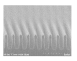
- (A) to (e) are sectional views schematically showing an example of a manufacturing process of a wire grid type polarizing element. Scanning electron microscope (SEM) photograph observed from diagonally above the substantially front surface of the mold used in Example 1.
- wire grid type polarizing element Each element and structure constituting the wire grid type polarizing element of the present invention will be described.
- the shape of the metal reflector (B) is not so-called “wire shape", but even when the metal reflector is not wire shape in the technical field, it is "wire grid type”. Since the term “polarizing element” is used, the term wire grid type polarizing element is used.
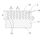
- FIG. 1 is a cross-sectional view schematically shown for explaining the wire grid type polarizing element (R1) 1 of the present invention, in which the sheet (A) 11 has a front surface side 12 and a back surface side 13.
- a metal reflector (B) 14 is embedded in the surface side 12.
- the metal reflector (B) 14 has a portion (D) 15 that gradually becomes thinner toward the tip.
- the average width (a), the average thickness (b), the average length (c) of the portion (D) 15 that gradually becomes thinner toward the tip, and the period (d) are displayed in other ways. It is also used in common in the form.
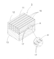
- FIG. 2 is a sectional view schematically showing the wire grid type polarizing element (R1) 2 for explanation as viewed from diagonally above. In FIG.
- the shape of the portion (D) 15 of the metal reflector (B) 14 that gradually becomes thinner toward the tip is a cross section perpendicular to the one-dimensional lattice arrangement direction, and the apex is in the tip direction. It is in the shape of a substantially inverted triangle located.
- FIG. 3 is an example of a sectional view schematically showing the wire grid type polarizing element (R2) 3 for explanation as viewed from diagonally above.
- the shape of the portion (D) 17 of the metal reflector (B) 16 that gradually becomes thinner toward the tip is a cross section in the one-dimensional lattice arrangement direction and perpendicular to the surface of the sheet (A).
- the vicinity of the tip is a continuous substantially triangular wave shape, and the vertices of these substantially triangular wave shapes are located in the tip direction.
- FIG. 4 is an example of an explanatory sectional view schematically showing a wire grid type polarizing element (R3).
- the shape of the portion (D) of the metal reflector (B) 18 that gradually becomes thinner toward the tip is a substantially quadrangular pyramid structure in which the apex is located in the tip direction, or a substantially quadrangular pyramid structure. It is a structure in which a structure that gradually changes in a substantially conical shape from the bottom surface toward the apex is continuous in the one-dimensional lattice-like arrangement direction.
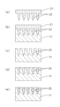
- FIG. 5 is a schematic cross-sectional surface showing an example of a manufacturing process of a wire grid type polarizing element.
- FIG. 5A shows a mold 21 having a convex portion 22 used when forming a groove portion (C) in the sheet (A) 11, and FIG. 5B shows the sheet (A) 11 by the nanoimprint method.
- 5 (c) shows the sheet (A) 11 on which the groove (C) 23 is formed
- FIG. 5 (d) shows the groove (C) 23 of the sheet (A).
- the state in which the ink 24 containing the metal fine particles is filled is shown
- FIG. 5 (e) shows the state in which the metal fine particles in the groove (C) 23 of the sheet (A) are fired to form a fired body 25.
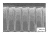
- FIGS. 6 to 12 are scanning electron microscope (SEM) photographs of the mold and the like used in the examples of the present specification, these photographs will be described in each embodiment.
- sheet (A) (1-1) Surface shape of sheet (A) Generally, when the thickness is 250 ⁇ m or less, it may be distinguished as a film, and when it is thicker than that, it may be distinguished as a sheet, but the sheet (A) of the present invention. Can be used for both sheets and films without distinguishing between them. Therefore, in the present specification, the sheets and films are collectively referred to as sheets.
- the surface shape of the sheet (A) is preferably flat from a practical point of view, and may be curved with a gentle curvature. Such a sheet (A) can easily form a groove (C) on the surface of the sheet (A) by a nanoimprint method or the like, and can easily perform a post-treatment step such as coating.
- the metal reflector (B) If the outer surface of the metal reflector (B) is almost flush with the surface of the sheet (A) and is embedded in the groove (C), it is scratch resistant and has a polarizing function even when rubbed or wiped. It is not easily affected and has excellent surface durability. Furthermore, the metal reflector (B) in the groove (C) is less likely to be oxidized, and its heat resistance and moisture resistance are also improved, so that it can be used outdoors or in a high temperature and high humidity environment. Can be maintained for a long time.
- the sheet (A) which is the base material of the wire grid type polarizing element of the present invention, has transparency in electromagnetic waves of a target wavelength such as a visible light region and an infrared region. Moreover, as long as it is possible to form a one-dimensional lattice-shaped groove portion described later on the surface of the sheet (A), either an organic material or an inorganic material can be used.
- the "transparent sheet (A)” means a sheet having transparency enough to maintain the transmittance required for the purpose of use, and is a transparent or translucent sheet, and a colorless or colored sheet. You may.
- the translucent sheet and the colored sheet can be easily manufactured by a known method.
- the organic materials that can be used include polycarbonate resin, polyacrylic resin, polyamide resin, polyester resin, polyolefin resin, polycycloolefin resin, polyurethane resin, cellulose resin, polyvinyl chloride resin, and poly.
- the use of ether-based resins, polyarylate-based resins, and polysulfon-based resins is preferable, but is not limited to these.
- the sheet (A) When polycarbonate or the like is used as the sheet (A), heat resistance, impact resistance, etc. can be improved, but coloring interference fringes are generated on the side where sunlight is incident and the degree of polarization when viewed from the transmission side. There was a problem of decline.
- a polycarbonate sheet or the like is obtained by extrusion molding or the like, it is preferable to stretch it in one direction to control the retardation value (the product of the birefringence of the sheet and the thickness).
- the retardation value is not particularly limited, but is preferably a very low value or a high value, and in the case of a high value, the extension axis of the base sheet (A) becomes the absorption axis of the wire grid type polarized light.
- the inorganic material that can be used include, but are not limited to, glass, silicon, quartz, and ceramic materials. Among the above materials, the use of an organic material is more preferable in consideration of processability such as formation of a groove (C). Further, the sheet (A) is preferably a single layer in consideration of expansion and contraction processes such as bending, but may be a plurality of layers.
- the constituent material of the metal reflector (B) used in the present invention reflects light in the wavelength range of the light to be used.
- Any metal material having a function can be used without particular limitation.
- Specific examples of the constituent materials include aluminum, nickel, chromium, platinum, palladium, titanium, gold, silver, copper, which are highly reflective metal materials, and a mixture of any one or more of these alloys. Further, examples thereof include molybdenum, tungsten, tantalum, zirconium, iron, niobium, hafnium, cobalt and the like, which are low-reflection metal materials, and alloys thereof.
- the use of a highly reflective metal material is preferable in consideration of polarization.
- the metal reflector (B) is formed by using a metal fine particle firing means or a plating means, it is desirable to select the metal reflector (B) in consideration of these processing means.
- the shape of the metal reflector (B) in the wire grid type polarizing element of the present invention is In a state of being embedded in a large number of grooves (C) provided in a one-dimensional lattice pattern in the same direction and at the same period on the surface of the transparent sheet (A).
- the average width (a) is 200 nm or less
- the ratio (b / a) of the average thickness (b) from the front surface side to the tip end in the back surface direction of the sheet (A) to the average width (a) is 4 or more and 25 or less.
- the shape of the metal reflector (B) in the vicinity of the tip in the thickness direction is gradually narrowed to a straight line or a smooth curve toward the tip.
- the ratio (c / a) of the average length (c) of the portion (D) gradually narrowing toward the tip in the tip direction and the average width (a) is 1.2 or more.
- the grid shape includes a one-dimensional grid shape, a two-dimensional grid shape, and the like.
- the two-dimensional grid shape refers to a state in which thin square members are assembled vertically and horizontally, and the one-dimensional grid shape is either of them. It refers to a state in which they are lined up with a gap in that direction, and the one-dimensional grid pattern of the present invention means the latter state.
- each metal reflector (B) in the groove portion (C) of the sheet (A) has the same orientation and the same period on the surface of the transparent sheet (A). It is necessary to arrange them in a one-dimensional grid pattern (striped pattern). Since the metal reflector (B) has the shape and structure described below and is embedded in the groove (C) of the sheet (A), it is scratch resistant and does not affect the polarization function even if it is rubbed or wiped. It is hard to come out and has excellent surface durability.
- Mean width (a) of the metal reflector (B) The average width (a) of each metal reflector (B) of the present invention is 200 nm or less in consideration of the degree of polarization and the light transmittance, the lower limit is preferably 25 nm or more, and the upper limit is preferably 100 nm or less.
- the groove width is preferably about 1/16 to 1/4 of the wavelength of the target electromagnetic wave. It has been known.
- Period of one-dimensional grid-like array of metal reflector (B) (d)
- the period (d) of the one-dimensional lattice array can be determined by the wavelength of the light intended to be polarized by the wire grid type polarizing element.
- the period (d) is 1/5 to 1/1 of the wavelength of the intended light. It can be about 2 or less.
- the ratio (d / a) of the period (d) of the one-dimensional lattice-like arrangement (B) to the average width (a) is preferably 1.3 or more and 20 or less, and further, considering the balance with the degree of polarization, the lower limit value. Is more preferably 2 or more, and the upper limit value is more preferably 8 or less.
- the average thickness (b) of the metal reflector (B) from the front surface side of the sheet (A) to the tip end in the back surface direction is a thickness of 4 or more and 25 or less in terms of the ratio (b / a) to the average width (a).
- the ratio (b / a) is 4 or more to improve the degree of polarization, and is 25 or less in consideration of mold processing and light transmittance. From a practical point of view, the lower limit is preferably 7 or more, and the upper limit is 20 or less is preferable.
- One of the features of the wire grid type polarizing element of the present invention is that the average thickness (b) of the metal reflector (B) is increased as described above in order to improve the degree of polarization of the light incident from the surface side. is there.
- the average length (c) of the portion (D) that gradually becomes thinner toward the tip is improved by setting the ratio (b / a) of the average thickness (b) and the average width (a) of the metal reflector (B) to 4 or more and 25 or less.
- One of the features is that it can be done.
- the shape of the metal reflector (B) near the tip in the thickness direction gradually becomes thinner toward the tip with a straight line or a smooth curve, and gradually becomes thinner toward the tip.
- the back surface is formed. It is possible to reduce the reflectance from the side. Further, the ratio (c / a) is preferably 1.2 or more and 8 or less in consideration of the reflectance of the wire grid type polarizing element to the back surface side with respect to the incident light from the back surface side, the workability of the mold, and the like.
- the lower limit value is more preferably 1.5 or more, and the upper limit value is more preferably 5 or less.
- V-1) Wire grid type polarizing element (R1) As shown in the cross-sectional view schematically shown in FIG. 2, the shape of the “thinning portion (D)” 15 of the metal reflector (B) 14 in the wire grid type polarizing element (R1) 2 is It is a substantially inverted triangle whose vertices are located in the tip direction in a cross-sectional shape perpendicular to the one-dimensional lattice arrangement direction. Further, in consideration of the reduction of the reflectance on the back surface side, the substantially inverted triangle is preferably a substantially inverted isosceles triangle.
- V-2) Wire grid type polarizing element (R2) As shown in the cross-sectional view schematically shown in FIG.
- the shape of the “thinning portion (D)” 17 of the metal reflector (B) 16 in the wire grid type polarizing element (R2) 3 is It is a continuous substantially triangular wave shape in which each apex is located in the tip direction in a cross-sectional shape perpendicular to the surface of the sheet (A) in a one-dimensional lattice arrangement direction. Considering the reduction of the reflectance on the back surface side, it is preferable that each substantially triangular wave shape is a substantially isosceles triangle shape.
- A' which is an enlarged view of the A portion, the shape of the tip portion of the substantially triangular wave shape is schematically shown so as to be three-dimensionally recognizable.
- each substantially quadrangular pyramid structure is a substantially regular quadrangular pyramid structure.
- the shape of the tip portion of the substantially quadrangular pyramid structure is schematically shown in B', which is an enlarged view of the B portion, so that the shape can be recognized three-dimensionally. It was. .. In any of the shapes shown in (v-1) to (v-3), the average length (c) of the metal reflector (B) in the tip direction of the "thinning portion (D)" Since the ratio (c / a) to the average width (a) is as described above, the angle of the tip portion in each of the cross sections is within a substantially common range, so that the back surface side of the wire grid type polarizing element The reflectance to the back surface side with respect to the incident light from is also reduced.
- the base length and height of a substantially triangular wave shape in the one-dimensional lattice arrangement direction and in the cross section perpendicular to the sheet (A) surface are more regular or irregular.
- the wire grid type polarizing element (R3) the base of each substantially quadrangular pyramid structure or a structure that gradually changes from the bottom surface of the substantially quadrangular pyramid structure toward the apex in a substantially conical shape.
- the width and height in the one-dimensional lattice arrangement direction can be further changed in a regular or irregular continuous manner.
- a metal reflector (a metal reflector (a metal reflector) is formed by using a plating means or a means for firing an ink containing metal fine particles in a one-dimensional lattice-shaped groove (C) provided in the transparent sheet (A). It is possible to form B). In particular, it is preferable to form the metal reflector (B) into a metal reflector made of a calcined metal fine particle by using a means for firing an ink containing metal fine particles as described later.
- the metal reflector (B) has an average width (a), an average thickness (b), and a portion (D) that gradually becomes thinner toward the tip in the groove portion (C) of the sheet (A). It is embedded in the shape of the average length (c) in the tip direction, but the metal reflector (B) may be embedded as a single continuous structure in each groove (C). Also, a plurality of block-shaped structures are embedded in a state of being laminated at a high density, and each block-shaped structure is laminated in a state of being independent of each other, or one of the outer surfaces of each block-shaped structure is one of them. The parts or all of them may be laminated in a joined state.
- the single continuous structure can be formed in the groove portion (C), and when the metal fine particles are formed by the firing means, the firing conditions By control, the plurality of block-shaped structures are laminated in the groove portion (C) in an independent state from each other, or a state in which a part or all of the outer surfaces thereof are joined to each other is formed. can do.
- (II) Method for manufacturing wire grid type polarizing element In the method for manufacturing the wire grid type polarizing element of the present invention, a large number of grooves are formed on the surface of a transparent sheet (A) in a one-dimensional lattice pattern in the same direction and with the same period by the nanoimprint method.
- the groove (C) is formed in a sheet (A) by the nanoimprint method.
- the structure of each convex portion forming a large number of grooves (C) in the mold used for forming the above has an average width (a') of 200 nm or less.
- the average length (b') in the tip direction is 4 or more and 25 or less in terms of the ratio (b'/ a') to the average width (a').
- the shape near the tip of each convex portion is a straight line or a smooth curve that gradually narrows toward the tip, and gradually narrows toward the tip (D') toward the tip.
- the ratio (c'/ a') of the average length (c') to the average width (a') is 1.2 or more.
- a metal reflector is formed in the grooves (C). It can be manufactured by embedding (B). It is generally known that nanoimprint method, injection molding, electron beam lithography, focused ion beam, exposure technology such as interference exposure, self-organization technology using nanoparticles and the like can be used for forming the groove portion (C). There is.
- a fine groove (C) is formed on the surface of a sheet (A) by using a nanoimprint method, and then a metal reflector (B) is embedded in the groove (C). It is a method, a simple and practical method.
- FIG. 5A is a schematic cross-sectional view of a mold 21 having a convex portion 22, and the mold 21 is used to transfer to the sheet (A) 11 as shown in FIG. 5B, and FIG. As shown in (c), the groove portion (C) 23 is formed in the sheet (A) 11. Next, as shown in FIG. 5 (d), the groove (C) is filled with the ink 24 containing the metal fine particles, and then the metal fine particles in the groove (C) are fired by the firing step, and FIG. 5 (e) shows. As shown, a fired body 25 of metal fine particles is formed in the groove portion (C).
- the structure of the convex portion of the mold has the same shape as the metal reflector (B) of the wire grid type polarizing element, the average width (a') and the average length (b') in the mold structure are formed. ), The average length (c') in the tip direction of the portion (D') that gradually becomes thinner toward the tip is the mean width (a) of the metal reflector (B) of the wire grid type polarizing element, respectively. ), The average thickness (b), and the average length (c) of the portion (D) that gradually becomes thinner toward the tip in the tip direction. Since the description of the convex structure of the mold is the same as the description of the structure of the metal reflector (B), the description here will be omitted.
- the first step is a step of forming a large number of grooves (C) on the surface of the transparent sheet (A) in a one-dimensional lattice pattern in the same direction and at the same period by the nanoimprint method.
- the structure of each convex portion forming the groove portion (C) in the mold used when forming the groove portion (C) on the sheet (A) has an average width (a') of 200 nm or less and an average in the tip direction.
- the length (b') is 4 or more and 25 or less in terms of the ratio (b'/ a') to the average width (a'), and the shape near the tip of the convex portion is linear or smooth toward the tip.
- the ratio of the average length (c') toward the tip of the portion (D') that gradually becomes thinner toward the tip and the mean width (a'). (C'/ a') is 1.2 or more.
- FIG. 5A shows a mold 21 having a convex portion 22 used when forming a groove portion (C) on the sheet (A) 11, and FIG. 5B shows a sheet by a nanoimprint method.
- FIG. 5 (c) shows the sheet (A) 11 in which the mold 21 is transferred to (A) 11 and the groove portion (C) 23 is formed.
- a pressure of about several MPa is usually applied, so silicon is preferable as the material of the mold, but it has a certain strength such as glass such as quartz, ceramics such as alumina and silicon carbide, and nickel. Those can be used, and a multi-layer material in which a metal, a semiconductor, or a dielectric is further deposited on these materials can also be used.
- the mold can be processed by using the above materials and utilizing a semiconductor or photomask manufacturing technique.
- the nanoimprint method uses thermal nanoimprint in which the sheet (A) is a thermoplastic resin or glass, and photocurable nanoimprint in which the material to be processed is a photocurable resin, and the microstructure of the mold is inverted as it is. Can be copied to the transfer target.
- thermosetting nanoimprint when the shape is transferred, if the thermoplastic resin to be processed is an amorphous resin, the rigidity and viscosity begin to decrease. The temperature and crystal are about 20 ° C higher than the glass transition temperature (Tg). In the case of a sex resin, it is desirable to transfer it in a state of being heated above the melting point.
- UV curable resin When UV curable resin is used in curable nanoimprint, quartz or the like that allows UV light to pass through is used as a mold, and the resin viscosity before curing is lower than that of thermal nanoimprint, so it has a fine shape and high aspect ratio. It has the characteristic that the shape of the ratio can be transferred well.
- a fluorine-based mold release agent As the mold release agent applied to the mold, while a silicon-based mold release agent is used depending on the mold (mold) material or the resin material to be molded. Can also be used.
- mass production is possible by a roll-to-roll method or a batch method.
- Second step step of embedding the metal reflector (B) in the groove (C)
- the means for embedding the metal reflector (B) in the groove portion (C) is not particularly limited, and known techniques such as firing means for metal fine particles, plating means, physical vapor deposition method, and chemical vapor deposition method can be used.
- firing means for metal fine particles is highly practical and relatively easy to operate. Therefore, a specific example using the means for firing metal fine particles as the second step will be described below.
- an ink or paste containing the metal fine particles (hereinafter, the ink and the paste are collectively referred to as an ink) is applied to the groove portion (C) of the sheet (A). It comprises a step of filling (filling step of ink) and a step of heating the filled ink to fire (firing) metal fine particles (baking step of metal fine particles).
- FIG. 5 (d) shows a state in which the groove (C) 23 of the sheet (A) is filled with the ink 24 containing metal fine particles
- FIG. 5 (e) shows the groove (C) of the sheet (A). The state in which the metal fine particles in 23 are fired to become the fired body 25 is shown.
- the ink has an average particle size of a metal reflector (B) in a solvent containing at least a dispersant such as an amine compound and gelatin that coats the surface of metal fine particles and an organic solvent having a high boiling point.
- a metal reflector (B) in which metal fine particles having an average width (a) or less, preferably 1/2 or less of the average width (a) are uniformly dispersed, and the metal fine particle content in the ink is about 60 to 90% by mass. It is desirable to use.
- the dispersant such as the amine compound is a dispersant containing at least one compound having a group containing nitrogen, oxygen, or a sulfur atom, and the organic solvent having a high boiling point is a non-polar solvent or a low-polar solvent, for example, carbon.
- Alkanes having several tens or more (for example, tetradecane) and primary alcohols having ten or more carbon atoms (for example, 1-decanol) are preferably used. Since the inks that can be used in the present invention are commercially available as shown in Examples, they are easily available.
- the metal fine particles are the same as the constituent materials of the metal reflector (B), and are preferably among highly reflective metal materials such as aluminum, nickel, chromium, platinum, palladium, titanium, gold, silver, copper, and alloys thereof. It is a mixture of any one or two or more of the above, and among these, silver is preferable in consideration of availability.
- the ink containing the above components can draw a fine pattern, and when the metal fine particles are heated and fired, the dispersant such as an amine compound is separated from the surface of the metal fine particles, so that the surface of the metal fine particles is activated. The firing is promoted.
- the width of the groove portion (C) is nano-sized, when filling the groove portion (C) of the sheet (A), it is possible to fill the groove portion (C) by utilizing the capillary phenomenon, so that the ink and the sheet can be filled. It is desirable to select an ink having a contact angle with (A) preferably 0 degrees or more and less than 90 degrees, and more preferably 0 degrees or more and 60 degrees or less. Further, considering that the wettability of the ink with the surface inside the groove (C) (contact angle with the ink) is larger than the wettability between the surface of the sheet (A) and the ink, it is easier to fill the ink.
- a liquid-repellent film on the surface of the sheet (A) so that the contact angle with the ink is larger than the contact angle of the ink with the surface inside the groove (C). It is desirable that the liquid-repellent film is provided before forming the groove (C) in the sheet (A), and as a specific method thereof, methane tetrafluoride (CF 4 ) is treated with a gaseous plasma treatment.
- CF 4 methane tetrafluoride
- a method of forming directly on the surface of a sheet a method of forming by diluting and dissolving organic silane in a fluorine-based solvent (organic silane concentration: about 0.1% by mass) on the sheet and then evaporating the fluorine-based solvent.
- the liquid-repellent film not only promotes filling of the ink groove (C), but also functions as a protective film for preventing the fired metal fine particles from adhering to unnecessary parts on the sheet (A). To do.
- a method of filling the groove (C) of the ink a method using a squeegee, a doctor blade or the like is preferable, but the ink and the groove (C) such as an inkjet method, droplet coating by a dispenser, spin coating, dip coating, etc. A method of contacting the structures can also be used.
- a liquid-repellent film is formed on the surface of the sheet (A)
- a method of directly wiping the surface of the sheet (A) is preferable, but polishing, ultrasonic cleaning, etc. Cleaning such as high-pressure jet cleaning or pressing an ink-absorbing material against the surface of the sheet (A) can also remove excess ink.
- (Ii) Firing step of metal fine particles In the calcining step of metal fine particles, the sheet (A) in which the groove (C) is filled with ink is heated to evaporate the dispersant and the organic solvent contained in the ink. This is a step of firing metal fine particles to form a metal reflector (B) in the groove portion (C). In the liquid phase firing, external pressure is often required because the capillarity of the liquid phase creates sufficient internal pressure between the solid phase particles (the magnitude of the capillary force corresponds to a very high external pressure). Do not.
- a firing device such as a hot plate, a plasma firing device, a microwave firing device, a farush lamp light firing device, or a laser firing device should be used. Is also possible.
- the firing temperature and the time required for firing depend on the components of the metal fine particles, the particle size, the dispersant used for the ink, and the organic solvent, but in general, the firing temperature is preferably 80 to 200 ° C, more preferably 100 to 160 ° C. Is.
- the firing time can be arbitrarily determined in consideration of the firing temperature.
- the degree of polarization, the light transmittance, and the light reflectance of the prepared test pieces were measured using the following devices.
- the visual transmittance of each polarized light can be obtained from the respective transmittance (transmission spectrum) and the luminosity curve when the wavelength is 380 to 780 nm (in 1 nm increments).
- Example 1 A fine groove structure is formed on the surface of the thermoplastic resin sheet by a thermal nanoimprint method using a mold, and then an ink containing silver fine particles is filled in the groove, and then the silver contained in the ink is placed in a heated oven.
- a polarizing element obtained by firing fine particles and having an irregularly continuous concave-convex shape at the tip of the wire grid type polarizing element (R1) type in a cross section perpendicular to the sheet surface in a one-dimensional lattice arrangement direction.
- R1 wire grid type polarizing element
- the average length (b') to the tip of the convex portion is 499.8 nm
- the average length (c') toward the tip of the portion that gradually becomes thinner toward the tip is 100 nm.
- the tip of the portion that gradually becomes thinner forms an uneven shape irregularly and continuously in the arrangement direction of the convex portions, and the height difference of the uneven shape is 90% or more and 120 nm or less.
- the ratio (c'/ b') of the average length (c') to the average length (b') of the metal reflector was 0.3 or less.
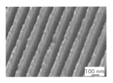
- FIG. 6 is a scanning electron microscope (SEM) photograph observed from diagonally above the front of the mold used in Example 1.
- FIG. 7 is an SEM photograph observed from diagonally above the mold used in Example 1.
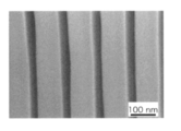
- FIG. 8 is a schematic front view of a transparent sheet having grooves formed by the nanoimprint method.
- Example 2 and 3 In Examples 2 and 3, as in Example 1, a fine groove structure is formed on the sheet surface using a mold, the groove is filled with ink, and then fired, and the same as in Example 1.
- the average length (b') to the tip of the convex portion is 499.8 nm in Example 2, 388.5 nm in Example 3, and the average length in the tip direction of the portion that gradually becomes thinner toward the tip ( c') is 100 nm in Example 2, 80 nm in Example 3, and the tip of the portion that gradually becomes thinner toward the tip forms an uneven shape irregularly and continuously in the arrangement direction of the convex portion.
- 90% or more of the height difference of the uneven shape is 120 nm or less, and in Example 3, 90% or more is 100 nm or less.
- the portion gradually becomes thinner toward the tip.
- the length (c') in the tip direction was within 0.3 times the average length (b'). Using each of these molds, the fine groove structure was transferred to the sheet surface by the thermal nanoimprint method.
- Example 1 the same silver nanoink as used in Example 1 was filled in the groove by the squeezing method, and after filling, excess ink adhering to other than the inside of the groove was removed by wiping.
- the sheet filled with the ink in the groove is fired in an oven heated to 130 ° C. for 81 hours in Example 2 and 12 hours in Example 3 to calcin the silver fine particles contained in the ink to obtain a polarizing element.
- a test piece was prepared.
- (2) Evaluation Results The degree of polarization, light transmittance, and light reflectance of the obtained polarizing element test piece were measured. These results are summarized in Table 1. As shown in Table 1, good results were obtained for both the degree of polarization and the reflectance on the back surface side of the polarizing element test pieces produced from the mold shapes used in Examples 2 and 3.
- a fine groove structure is formed on the surface of the thermoplastic resin sheet by a thermal nanoimprint method using a mold, and then an ink containing silver fine particles is filled in the groove, and then the silver contained in the ink is placed in a heated oven.
- a polarizing element test piece obtained by firing fine particles and having the tip of the wire grid type polarizing element (R1) type having a one-dimensional lattice-like arrangement direction and a cross section perpendicular to the sheet surface with a substantially linear tip. Made.
- Example 2 the same silver nanoink as used in Example 1 was filled in the groove by the squeezing method, and after filling, excess ink adhering to other than the inside of the groove was removed by wiping.
- the sheet filled with the ink in the groove was fired together with the silver fine particles contained in the ink in an oven heated to 130 ° C. for 12 hours to prepare a polarizing element test piece.
- the degree of polarization, light transmittance, and light reflectance of the obtained polarizing element test piece were measured. These results are summarized in Table 1. With respect to the polarizing element test piece produced from the mold having the shape used in Examples 4 and 5, good results were obtained in both the degree of polarization and the reflectance on the back surface side.
- Example 7 A fine groove structure is formed on the surface of the thermoplastic resin sheet by a thermal nanoimprint method using a mold, and then an ink containing silver fine particles is filled in the groove, and then the silver contained in the ink is placed in a heated oven. The fine particles were fired to prepare a polarizing element test piece of the wire grid type polarizing element (R3) type.
- the convex portion shape forming the groove portion has an inverted shape of the groove shape formed in the wire grid type polarizing element (R3) type, and the average width (a'), The average length (b'), the average length of the part that gradually becomes thinner toward the tip (c'), and the period of the arrangement (d') are as shown in Table 1 and its notes. Is.
- the shape is such that the width in the one-dimensional lattice arrangement direction and the height in the tip direction of the base of the structure changing in a substantially conical shape are irregularly and continuously changed.
- the height difference of 90% or more is 120 nm or less, and the average length (c') of the portion gradually narrowing toward the tip and the average length (b') of the metal reflector.
- the ratio (c'/ b') to and was 0.3 or less.
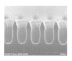
- FIG. 11 is a scanning electron microscope (SEM) photograph observed from diagonally above the front of the mold used in Example 8.
- Example 1 the same silver nanoink as used in Example 1 was filled in the groove by the squeezing method, and after filling, excess ink adhering to other than the inside of the groove was removed by wiping.
- the sheet filled with the ink in the groove was fired in an oven heated to 130 ° C. for 128 hours in Example 7 and 81 hours in Examples 8 and 9, and the silver fine particles contained in the ink were fired.
- a polarizing element test piece was prepared.
- (2) Evaluation Results The degree of polarization, light transmittance, and light reflectance of the obtained polarizing element test piece were measured. These results are summarized in Table 1. For the polarizing element test pieces prepared from the molds used in Examples 7 to 9, good results were obtained in both the degree of polarization and the reflectance on the back surface side.
- thermoplastic resin sheet A fine groove structure is formed on the surface of the thermoplastic resin sheet by a thermal nanoimprint method using a mold, and then an ink containing silver fine particles is filled in the groove, and then the silver contained in the ink is placed in a heated oven.
- a polarizing element test piece obtained by firing fine particles which is the wire grid type polarizing element (R1) type and has a substantially linear shape at the tip in a one-dimensional lattice-like arrangement direction and a cross section perpendicular to the sheet surface. Made.
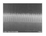
- Example 2 Preparation of Polarizing Element Test Piece A sheet similar to that used in Example 1 was used. As shown in Table 1 and its notes, the microstructure of the mold used has a convex shape in which the groove is formed, which is an inverted shape of the groove formed in the wire grid type polarizing element (R1) type. The average width (a'), the average length (b'), the average length of the portion that gradually becomes thinner toward the tip (c'), and the period of the arrangement (d'). Is as shown in Table 1 and its notes. Using each of these molds, the fine groove structure was transferred to the sheet surface by the thermal nanoimprint method. Further, FIG. 12 is a scanning electron microscope (SEM) photograph observed from diagonally above the front of the mold used in Comparative Example 2.
- SEM scanning electron microscope
- Example 1 the same silver nanoink as used in Example 1 was filled in the groove by the squeezing method, and after filling, excess ink adhering to other than the inside of the groove was removed by wiping.
- the sheet filled with the ink in the groove is fired in an oven heated to 130 ° C. for 12 hours in Comparative Example 1 and 81 hours in Comparative Example 2 to polarize the silver fine particles contained in the ink.
- a device test piece was prepared.
- (2) Evaluation Results The degree of polarization, light transmittance, and reflectance of the obtained polarizing element test piece were measured. These results are summarized in Table 1.
- the degree of polarization decreases when the ratio (b / a) of the average thickness (b) of the metal reflector to the average width (a) is 3.5. It was confirmed that Further, in the polarizing element test piece obtained from the mold shape used in Comparative Examples 1 and 2, the average length (c) and the average width (a) of the portion gradually becoming thinner toward the tip in the tip direction. It was confirmed that when the ratio (c / a) of was 1.0, the reflectance on the back surface side was slightly higher, and when it was 0.89, the reflectance on the back surface side was further increased.
- the wire grid type polarizing element of the present invention has excellent polarization performance, can maintain the required light transmittance, and has low reflectance on the back surface side, so that it is not limited to optical products such as various displays, cameras, and optical measuring instruments. It can be expected to be applied to polarized sunglasses, smart windows, etc.
Landscapes
- Physics & Mathematics (AREA)
- General Physics & Mathematics (AREA)
- Optics & Photonics (AREA)
- Polarising Elements (AREA)
Priority Applications (3)
| Application Number | Priority Date | Filing Date | Title |
|---|---|---|---|
| CN202080043060.5A CN114008495B (zh) | 2019-06-25 | 2020-05-14 | 线栅型偏振元件及其制造方法 |
| KR1020217037587A KR102851295B1 (ko) | 2019-06-25 | 2020-05-14 | 와이어 그리드형 편광 소자 및 그 제조 방법 |
| US17/535,744 US12189162B2 (en) | 2019-06-25 | 2021-11-26 | Wire-grid polarizer and process for producing the same |
Applications Claiming Priority (2)
| Application Number | Priority Date | Filing Date | Title |
|---|---|---|---|
| JP2019117465A JP7477085B2 (ja) | 2019-06-25 | 2019-06-25 | ワイヤグリッド型偏光素子、及びその製造方法 |
| JP2019-117465 | 2019-06-25 |
Related Child Applications (1)
| Application Number | Title | Priority Date | Filing Date |
|---|---|---|---|
| US17/535,744 Continuation US12189162B2 (en) | 2019-06-25 | 2021-11-26 | Wire-grid polarizer and process for producing the same |
Publications (1)
| Publication Number | Publication Date |
|---|---|
| WO2020261791A1 true WO2020261791A1 (ja) | 2020-12-30 |
Family
ID=74060871
Family Applications (1)
| Application Number | Title | Priority Date | Filing Date |
|---|---|---|---|
| PCT/JP2020/019185 Ceased WO2020261791A1 (ja) | 2019-06-25 | 2020-05-14 | ワイヤグリッド型偏光素子、及びその製造方法 |
Country Status (6)
| Country | Link |
|---|---|
| US (1) | US12189162B2 (enExample) |
| JP (1) | JP7477085B2 (enExample) |
| KR (1) | KR102851295B1 (enExample) |
| CN (1) | CN114008495B (enExample) |
| TW (1) | TWI733461B (enExample) |
| WO (1) | WO2020261791A1 (enExample) |
Citations (7)
| Publication number | Priority date | Publication date | Assignee | Title |
|---|---|---|---|---|
| JP2004309903A (ja) * | 2003-04-09 | 2004-11-04 | Ricoh Opt Ind Co Ltd | 無機偏光素子および偏光光学素子および液晶素子 |
| JP2006308668A (ja) * | 2005-04-26 | 2006-11-09 | Ricoh Co Ltd | 微細パターン形成プラスチックフィルムおよび埋め込み微細パターンの形成方法 |
| JP2009244312A (ja) * | 2008-03-28 | 2009-10-22 | Asahi Kasei E-Materials Corp | ワイヤグリッド型偏光子 |
| JP2010204297A (ja) * | 2009-03-02 | 2010-09-16 | Teijin Ltd | ワイヤーグリッド偏光子及びその製造方法 |
| JP2011170136A (ja) * | 2010-02-19 | 2011-09-01 | Seiko Epson Corp | 偏光素子及びプロジェクター |
| JP2012073484A (ja) * | 2010-09-29 | 2012-04-12 | Asahi Glass Co Ltd | ワイヤグリッド型偏光子および液晶表示装置 |
| JP2018159880A (ja) * | 2017-03-23 | 2018-10-11 | 日本ゼオン株式会社 | 円偏光フィルム及びその製造方法 |
Family Cites Families (16)
| Publication number | Priority date | Publication date | Assignee | Title |
|---|---|---|---|---|
| JP4386413B2 (ja) * | 2003-08-25 | 2009-12-16 | 株式会社エンプラス | ワイヤーグリッド偏光子の製造方法 |
| JP2006058615A (ja) * | 2004-08-20 | 2006-03-02 | Sumitomo Chemical Co Ltd | 金属細線が埋め込まれた偏光分離素子 |
| US7961393B2 (en) | 2004-12-06 | 2011-06-14 | Moxtek, Inc. | Selectively absorptive wire-grid polarizer |
| US20080129931A1 (en) * | 2004-12-16 | 2008-06-05 | Toray Industries, Inc. A Corporation Of Japan | Polarizer, Method For Producing The Same, And Liquid Crystal Display Device Using The Same |
| CN1952700B (zh) * | 2005-10-17 | 2010-06-09 | 旭化成电子材料株式会社 | 线栅偏振片及其制造方法 |
| JP5096735B2 (ja) | 2006-12-05 | 2012-12-12 | Jx日鉱日石エネルギー株式会社 | ワイヤグリッド型偏光子及びその製造方法、並びにそれを用いた位相差フィルム及び液晶表示素子 |
| JP2009204894A (ja) | 2008-02-28 | 2009-09-10 | Sony Corp | ワイヤグリッド偏光素子及びその製造方法、液晶ディスプレイ |
| JP5368011B2 (ja) | 2008-06-12 | 2013-12-18 | 旭化成イーマテリアルズ株式会社 | 吸収型ワイヤグリッド偏光子 |
| WO2010005059A1 (ja) | 2008-07-10 | 2010-01-14 | 旭硝子株式会社 | ワイヤグリッド型偏光子およびその製造方法 |
| JP5291425B2 (ja) | 2008-10-03 | 2013-09-18 | 旭化成イーマテリアルズ株式会社 | 吸収型ワイヤグリッド偏光子及び液晶表示装置 |
| JP5291424B2 (ja) | 2008-10-03 | 2013-09-18 | 旭化成イーマテリアルズ株式会社 | 吸収型ワイヤグリッド偏光子及び液晶表示装置 |
| JP2010204626A (ja) * | 2009-02-05 | 2010-09-16 | Asahi Glass Co Ltd | ワイヤグリッド型偏光子およびその製造方法 |
| JP2012098703A (ja) | 2010-10-04 | 2012-05-24 | Hoya Corp | 偏光素子 |
| KR101416628B1 (ko) * | 2012-12-10 | 2014-07-08 | 한국전기연구원 | 와이어 그리드 편광자의 제조 장치 및 방법 |
| KR20160069048A (ko) * | 2014-12-05 | 2016-06-16 | 삼성디스플레이 주식회사 | 와이어 그리드 편광자 및 이의 제조방법 |
| JP2016191805A (ja) * | 2015-03-31 | 2016-11-10 | 大日本印刷株式会社 | 偏光子、偏光子の製造方法及び液晶表示装置 |
-
2019
- 2019-06-25 JP JP2019117465A patent/JP7477085B2/ja active Active
-
2020
- 2020-05-14 KR KR1020217037587A patent/KR102851295B1/ko active Active
- 2020-05-14 WO PCT/JP2020/019185 patent/WO2020261791A1/ja not_active Ceased
- 2020-05-14 CN CN202080043060.5A patent/CN114008495B/zh active Active
- 2020-05-22 TW TW109117057A patent/TWI733461B/zh active
-
2021
- 2021-11-26 US US17/535,744 patent/US12189162B2/en active Active
Patent Citations (7)
| Publication number | Priority date | Publication date | Assignee | Title |
|---|---|---|---|---|
| JP2004309903A (ja) * | 2003-04-09 | 2004-11-04 | Ricoh Opt Ind Co Ltd | 無機偏光素子および偏光光学素子および液晶素子 |
| JP2006308668A (ja) * | 2005-04-26 | 2006-11-09 | Ricoh Co Ltd | 微細パターン形成プラスチックフィルムおよび埋め込み微細パターンの形成方法 |
| JP2009244312A (ja) * | 2008-03-28 | 2009-10-22 | Asahi Kasei E-Materials Corp | ワイヤグリッド型偏光子 |
| JP2010204297A (ja) * | 2009-03-02 | 2010-09-16 | Teijin Ltd | ワイヤーグリッド偏光子及びその製造方法 |
| JP2011170136A (ja) * | 2010-02-19 | 2011-09-01 | Seiko Epson Corp | 偏光素子及びプロジェクター |
| JP2012073484A (ja) * | 2010-09-29 | 2012-04-12 | Asahi Glass Co Ltd | ワイヤグリッド型偏光子および液晶表示装置 |
| JP2018159880A (ja) * | 2017-03-23 | 2018-10-11 | 日本ゼオン株式会社 | 円偏光フィルム及びその製造方法 |
Also Published As
| Publication number | Publication date |
|---|---|
| KR102851295B1 (ko) | 2025-08-27 |
| JP7477085B2 (ja) | 2024-05-01 |
| KR20220021908A (ko) | 2022-02-22 |
| TWI733461B (zh) | 2021-07-11 |
| CN114008495B (zh) | 2024-08-09 |
| TW202101068A (zh) | 2021-01-01 |
| JP2021004928A (ja) | 2021-01-14 |
| US12189162B2 (en) | 2025-01-07 |
| CN114008495A (zh) | 2022-02-01 |
| US20220082750A1 (en) | 2022-03-17 |
Similar Documents
| Publication | Publication Date | Title |
|---|---|---|
| JP5636963B2 (ja) | ワイヤグリッド型偏光子およびその製造方法 | |
| CN102084275B (zh) | 线栅型偏振器及其制造方法 | |
| CN101981479A (zh) | 线栅型偏振器及其制造方法 | |
| JP6014939B2 (ja) | 反射型偏光板の製造方法およびディスプレイ装置 | |
| US10151863B2 (en) | Optical grating | |
| CN101981478A (zh) | 线栅型偏振器的制造方法 | |
| WO2010126110A1 (ja) | ワイヤグリッド型偏光子およびその製造方法 | |
| KR101229673B1 (ko) | 저반사 및 고접촉각을 갖는 기판 및 이의 제조방법 | |
| CN102713697A (zh) | 线栅型偏振片及其制造方法 | |
| JP2003302532A (ja) | 偏光板およびその製造方法 | |
| CN113050204B (zh) | 一种微透镜阵列基板、3d显示装置及其制备方法 | |
| JP5833301B2 (ja) | ワイヤグリッド偏光板及びワイヤグリッド偏光板の製造方法 | |
| US12189162B2 (en) | Wire-grid polarizer and process for producing the same | |
| JP2021004928A5 (enExample) | ||
| JP2012073484A (ja) | ワイヤグリッド型偏光子および液晶表示装置 | |
| JP2011227130A (ja) | ワイヤグリッド型偏光子の製造方法 | |
| JP7240357B2 (ja) | 偏光素子、偏光素子の製造方法及びヘッドアップディスプレイ装置 | |
| JP2022001890A (ja) | ワイヤグリッド型偏光子 |
Legal Events
| Date | Code | Title | Description |
|---|---|---|---|
| 121 | Ep: the epo has been informed by wipo that ep was designated in this application |
Ref document number: 20830973 Country of ref document: EP Kind code of ref document: A1 |
|
| NENP | Non-entry into the national phase |
Ref country code: DE |
|
| 122 | Ep: pct application non-entry in european phase |
Ref document number: 20830973 Country of ref document: EP Kind code of ref document: A1 |
|
| WWG | Wipo information: grant in national office |
Ref document number: 1020217037587 Country of ref document: KR |