WO2020241474A1 - 電子制御装置 - Google Patents
電子制御装置 Download PDFInfo
- Publication number
- WO2020241474A1 WO2020241474A1 PCT/JP2020/020238 JP2020020238W WO2020241474A1 WO 2020241474 A1 WO2020241474 A1 WO 2020241474A1 JP 2020020238 W JP2020020238 W JP 2020020238W WO 2020241474 A1 WO2020241474 A1 WO 2020241474A1
- Authority
- WO
- WIPO (PCT)
- Prior art keywords
- control device
- electronic control
- fixture
- cover
- facing
- Prior art date
Links
Images


Classifications
-
- H—ELECTRICITY
- H05—ELECTRIC TECHNIQUES NOT OTHERWISE PROVIDED FOR
- H05K—PRINTED CIRCUITS; CASINGS OR CONSTRUCTIONAL DETAILS OF ELECTRIC APPARATUS; MANUFACTURE OF ASSEMBLAGES OF ELECTRICAL COMPONENTS
- H05K9/00—Screening of apparatus or components against electric or magnetic fields
- H05K9/0067—Devices for protecting against damage from electrostatic discharge
-
- H—ELECTRICITY
- H05—ELECTRIC TECHNIQUES NOT OTHERWISE PROVIDED FOR
- H05K—PRINTED CIRCUITS; CASINGS OR CONSTRUCTIONAL DETAILS OF ELECTRIC APPARATUS; MANUFACTURE OF ASSEMBLAGES OF ELECTRICAL COMPONENTS
- H05K7/00—Constructional details common to different types of electric apparatus
- H05K7/20—Modifications to facilitate cooling, ventilating, or heating
-
- H—ELECTRICITY
- H05—ELECTRIC TECHNIQUES NOT OTHERWISE PROVIDED FOR
- H05K—PRINTED CIRCUITS; CASINGS OR CONSTRUCTIONAL DETAILS OF ELECTRIC APPARATUS; MANUFACTURE OF ASSEMBLAGES OF ELECTRICAL COMPONENTS
- H05K9/00—Screening of apparatus or components against electric or magnetic fields
Definitions
- the present invention relates to an electronic control device.
- in-vehicle electronic control devices have been integrated into mechanical and electrical devices against the background of an increase in the number of electronic control devices mounted on vehicles and a reduction in the length of connection cables between control devices and sensors and actuators.
- the actuator for engine control and the electronic control device are integrated, and the transmission and the electronic control device are integrated.
- the surface temperature of the engine, the transmission, etc. is about 130 ° C. to 140 ° C.
- the heat resistant temperature of the electronic parts used in the electronic control device is about 150 ° C.
- the heat of the engine, transmission, etc. is transferred to the electronic components on the substrate held by the base via the base (housing) of the electronic control device.
- the temperature of electronic components may exceed the heat resistant temperature.
- An object of the present invention is to provide an electronic control device capable of suppressing a failure of an electronic component due to static electricity.
- the present invention comprises a substrate, electronic components mounted on the substrate, an insulating base for holding the substrate, and a conductive fixture for fixing the substrate to the base.
- an electronic control device including a conductive cover that covers the base, the distance D1 between the fixture and the cover is equal to or less than the distance D2 between the electronic component 1 and the cover.
- FIG. 5 is an enlarged cross-sectional view showing a configuration around a boss of an electronic control device according to a third embodiment. It is a figure for demonstrating the magnitude relation of area.
- FIG. 5 is an enlarged cross-sectional view showing a configuration around a boss facing a fixture of an electronic control device according to a modified example of the third embodiment.
- FIG. 7A It is a top view of the substrate shown in FIG. 7A. It is a schematic diagram which shows the example which connects the fixture to the ground. It is a schematic diagram which shows the modification which connects the fixture to the ground.
- FIG. 5 is an enlarged cross-sectional view showing a configuration around a boss of an electronic control device according to a modified example of the first embodiment. It is a figure for demonstrating the static electricity stored in the part of a cover facing a fixture.
- the electronic control device controls actuators such as an engine and a transmission, for example.
- actuators such as an engine and a transmission, for example.
- the same reference numerals indicate the same parts.
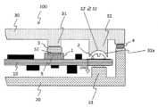
- FIG. 1 is a cross-sectional view showing the overall configuration of the electronic control device 100 according to the first embodiment of the present invention.
- the electronic control device 100 mainly includes a substrate 10, an electronic component 1 mounted on the substrate 10, an insulating base 20 for holding the substrate 10, and a conductive fixture 2 for fixing the substrate 10 to the base 20.
- a conductive cover 30 for covering the base 20 is provided.
- the insulating base 20 is made of, for example, an insulating resin, and is directly attached to an engine, a transmission, or the like. By making the base 20 made of resin, it becomes difficult for heat from the engine, transmission, etc. to be transferred to the electronic component 1.
- the thermal conductivity of the base 20 is smaller than the thermal conductivity of the cover 30, and is also smaller than the thermal conductivity of the housing of the engine, transmission, and the like.
- the conductive fixture 2 (screws, rivets, caulking, etc.) is made of, for example, a conductive metal or resin.
- the conductive cover 30 is made of, for example, a conductive metal (aluminum, steel, steel plate, etc.) or a conductive resin, and is molded by casting, pressing, injection molding, or the like.
- the electronic component 1 is mounted on the substrate 10.
- the electronic component 1 is composed of, for example, a semiconductor element.
- Specific examples of the electronic component 1 include a processor that calculates the control amount of the actuator from the output values of various sensors (temperature sensor, pressure sensor, etc.), a driver circuit that supplies a drive current to the actuator by switching, and the like.
- the driver circuit may be mounted on the actuator.
- the electronic component 1 is electrically connected to an actuator such as an engine or a transmission via a wiring pattern of a substrate 10, a pin of a connector 40, or the like.
- the electronic component 1 has a conductive exposed pad 5 facing the cover 30.
- the exposed pad 5 is, for example, a conductive metal plate, and is also called a heat spreader or a heat sink.
- the exposed pad 5 transfers the heat generated by the electronic component 1 to the conductive cover 30 via the heat conductive material 3. Then, the heat transferred to the cover 30 is dissipated into the atmosphere.
- the heat conductive material 3 contains ceramics and the like.
- the cover 30 is formed with a boss 31 facing the electronic component 1 and a boss 32 facing the conductive fixture 2.
- a heat conductive material 3 is arranged between the boss 31 and the electronic component 1.
- the sealing material 4 seals between the cover 30 and the base 20 and waterproofs the inside of the housing composed of the cover 30 and the base 20.
- the sealing material 4 is, for example, a silicone adhesive.
- the plurality of sets of bosses 32 and fixtures 2 are arranged at the corners of the substrate 10.
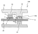
- FIG. 2 is an enlarged cross-sectional view showing the configuration around the boss 32 of the electronic control device 100 shown in FIG.
- the distance D1 between the fixture 2 and the cover 30 is equal to or less than the distance D2 between the electronic component 1 and the cover 30 (boss 31).
- the static electricity applied to the conductive cover 30 is more likely to be discharged to the fixture 2 than to the electronic component 1. Therefore, it is possible to prevent the electronic component 1 from failing due to static electricity. In addition, it is possible to prevent the electronic component 1 from malfunctioning due to static electricity.
- a gap is provided between the boss 32, which is a part of the cover 30 facing the fixture 2, and the fixture 2. As a result, the boss 32 does not come into contact with the fixture 2, so that the boss 32 does not deform the substrate 10. As a result, it is possible to prevent cracks from occurring in the solder (joining member) that joins the terminal of the electronic component 1 and the wiring pattern.
- the present embodiment it is possible to prevent the electronic component 1 from failing due to static electricity. In addition, it is possible to prevent the electronic component 1 from malfunctioning due to static electricity. Further, it is possible to suppress the occurrence of cracks in the solder that joins the terminal of the electronic component 1 and the wiring pattern.
- FIG. 3 is an enlarged cross-sectional view showing the configuration around the boss 32 of the electronic control device 100 according to the second embodiment of the present invention.
- the boss 32 which is a portion of the cover 30 facing the fixture 2, has a recess 32a that covers the head of the fixture 2.
- the area of the portion of the cover 30 facing the fixture 2 can be increased.
- the capacitance between the boss 32 and the fixture 2 becomes large, so that the static electricity applied to the conductive cover 30 is more easily discharged to the fixture 2 than the electronic component 1.
- the recess 32a of the boss 32 is composed of a surface that imitates the head of the fixture 2.
- the concave portion 32a is formed on a surface corresponding to the shape of each head.
- the portion of the cover 30 facing the fixture 2 can be brought closer to the surface of the head of the fixture 2 as a whole.
- the capacitance between the boss 32 and the fixture 2 can be further increased.
- the head of the fixture 2 is dome-shaped, and the recess 32a is also dome-shaped accordingly.
- the capacitance of the portion of the cover 30 (dome-shaped recess 32a) facing the fixture 2 can be increased.
- the electronic component 1 has a conductive exposed pad 5 facing the cover 30.
- the area S2 of the portion (recessed portion 32a) of the cover 30 facing the fixture 2 is equal to or larger than the area S1 of the exposed pad 5.
- the area S2 of the portion (recessed portion 32a) of the cover 30 facing the fixture 2 is such that the electronic component 1 is the heat conductive material 3.
- the area of the contacted or joined portion may be S3 or more.
- FIG. 5 is an enlarged cross-sectional view showing the configuration around the boss 32 of the electronic control device 100 according to the third embodiment of the present invention.
- the present embodiment is different from the second embodiment in that the dielectric material 6 is arranged between the boss 32 and the fixture 2.
- the heat conductive material 3 is arranged between the cover 30 and the electronic component 1.
- the sealing material 4 seals between the cover 30 and the base 20.
- the dielectric material 6 is arranged between the portion of the cover 30 (recessed portion 32a) facing the fixture 2 and the head of the fixture 2.
- the relative permittivity ⁇ 3 of the dielectric material 6 is the same as or larger than the relative permittivity ⁇ 1 of the heat conductive material 3 or the relative permittivity ⁇ 2 of the sealing material 4. As a result, the capacitance between the boss 32 and the fixture 2 can be further increased.
- the electronic component 1 has a conductive exposed pad 5 facing the cover 30.
- the area S2_1 of the portion (recessed portion 32a) of the cover 30 facing the fixture 2 and contacting or joining with the dielectric material 6 is equal to or larger than the area S1 of the exposed pad 5.
- the capacitance between the boss 32 and the fixture 2 can be further increased.
- FIG. 7A is an enlarged cross-sectional view showing the configuration around the boss 32 of the electronic control device 100 according to the modified example of the third embodiment.
- FIG. 7B is a plan view of the substrate 10 shown in FIG. 7A.
- the fixture 2 (2 1 to 2 5) is multiple (five). Then, L5 ⁇ L1 ⁇ L4 ⁇ L2 ⁇ L3 is established for the distance L (L1 to L5) between the electronic component 1 and the fixture 2 (2 1 to 25 ). That is, the portion of the cover 30 (boss 32) facing the fixture 2 faces the portion of the plurality of fixtures 2 closest to the electronic component 1 (fixer 25 ).
- At least one set of bosses 32 and the fixture 2 are arranged near the electronic component 1 in the third embodiment, but at least one set of bosses 32 and the fixture 2 are arranged in the first to second embodiments.
- the fixture 2 may be placed near the electronic component 1.
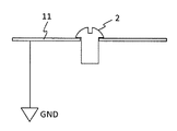
- FIG. 8A is a schematic view showing an example of connecting the fixture 2 to the ground.
- the substrate 10 has a wiring pattern 11.
- the fixture 2 is connected to the ground via the wiring pattern 11.
- the static electricity discharged from the boss 32 to the fixture 2 is discharged to the ground. That is, it is possible to secure a discharge path for static electricity to the circuit ground.
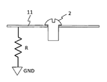
- FIG. 8B is a schematic view showing a modified example of connecting the fixture 2 to the ground.
- the substrate 10 has a wiring pattern 11 and a circuit element (resistor R) connected to the wiring pattern 11.
- the fixture 2 is connected to the ground via the wiring pattern 11 and the circuit element (resistor R).
- resistor R As a result, static electricity is converted into heat energy in the circuit element (resistor R), and fluctuations in the ground potential can be suppressed.
- a switching element, a capacitor, or the like may be used as the circuit element instead of the resistor R.
- FIG. 9 is an enlarged cross-sectional view showing the configuration around the boss 32 of the electronic control device 100 according to the modified example of the first embodiment.
- the area S2 of the part (boss 32) of the cover 30 facing the fixture 2 is equal to or larger than the area S0 of the part of the cover 30 facing the electronic component 1, or the electronic component 1 contacts or joins with the heat conductive material 3.
- the area of the portion is S3 or more.
- the static electricity 7a applied to the cover 30 is stored in the portion (boss 32) of the cover 30 facing the fixture 2, and is discharged to the fixture 2 due to dielectric breakdown.
- the capacitance between the boss 32 and the fixture 2 is combined. As a result, more static electricity 7a can be stored in the portion of the cover 30 facing the fixture 2.
- the present invention is not limited to the above-described embodiment, and includes various modifications.
- the above-described embodiment has been described in detail in order to explain the present invention in an easy-to-understand manner, and is not necessarily limited to the one including all the described configurations.
- it is possible to replace a part of the configuration of one embodiment with the configuration of another embodiment and it is also possible to add the configuration of another embodiment to the configuration of one embodiment.
Abstract
静電気により電子部品が故障することを抑制することができる電子制御装置を提供する。 電子制御装置100は、基板10と、基板10に実装される電子部品1と、基板10を保持する絶縁性のベース20と、基板10をベース20に固定する導電性の固定具2と、ベース20を覆う導電性のカバー30を備える。固定具2とカバー30(ボス32)との間の距離D1は、電子部品1とカバー30(ボス31)との間の距離D2以下である。
Description
本発明は、電子制御装置に関する。
近年、車載用電子制御装置は、車両に搭載する電子制御装置数の増大及び、制御装置とセンサ間、アクチュエータ間の接続ケーブル長さの短縮などを背景とした機電一体化が進んでいる。具体的には、エンジン制御用アクチュエータと電子制御装置の一体、変速機と電子制御装置の一体などである。
ここで、エンジン及び変速機等の表面温度は130℃~140℃程度であるが、これに対し、電子制御装置に用いられる電子部品の耐熱温度は、約150℃である。
このような過酷な環境で電子制御装置を作動させると、エンジン、変速機などの熱が、電子制御装置のベース(筐体)を介して、ベースによって保持される基板上の電子部品に伝わり、電子部品の温度が耐熱温度を超えるおそれがある。
特許文献1に開示されるような電子制御装置では、基板を保持するベースは金属製(合金製)であるため、エンジン、変速機などの熱がベース(筐体)を介して電子部品に伝わり易い。そこで、エンジン、変速機などの熱による電子部品の温度上昇を抑制するため、電子制御装置のベースを樹脂製とすることが考えられる。
しかし、ユーザの手などから金属製のカバーに付与された静電気が、樹脂製のベースに放電されないという新たな課題が生じる。また、静電気が電子部品に放電され、電子部品が故障することが懸念される。
本発明の目的は、静電気により電子部品が故障することを抑制することができる電子制御装置を提供することにある。
上記目的を達成するために、本発明は、基板と、前記基板に実装される電子部品と、前記基板を保持する絶縁性のベースと、前記基板を前記ベースに固定する導電性の固定具と、前記ベースを覆う導電性のカバーと、を備える電子制御装置において、前記固定具と前記カバーとの間の距離D1は、前記電子部品1と前記カバーとの間の距離D2以下である。
本発明によれば、静電気により電子部品が故障することを抑制することができる。上記した以外の課題、構成及び効果は、以下の実施形態の説明により明らかにされる。
以下、図面を用いて、本発明の第1~第3の実施形態による電子制御装置の構成を説明する。電子制御装置は、例えば、エンジン、変速機などのアクチュエータを制御する。なお、各図において、同一符号は同一部分を示す。
(第1の実施形態)
はじめに、図1を用いて、第1の実施形態による電子制御装置100の構成を説明する。図1は、本発明の第1の実施形態による電子制御装置100の全体構成を示す断面図である。
はじめに、図1を用いて、第1の実施形態による電子制御装置100の構成を説明する。図1は、本発明の第1の実施形態による電子制御装置100の全体構成を示す断面図である。
電子制御装置100は、主として、基板10と、基板10に実装される電子部品1と、基板10を保持する絶縁性のベース20と、基板10をベース20に固定する導電性の固定具2と、ベース20を覆う導電性のカバー30を備える。
絶縁性のベース20は、例えば、絶縁性の樹脂でできており、エンジン、変速機などに直付けされる。ベース20を樹脂製とすることで、エンジン、変速機などからの熱が電子部品1へ伝わりにくくなる。ベース20の熱伝導率は、カバー30の熱伝導率よりも小さく、またエンジン、変速機などのハウジングの熱伝導率よりも小さい。
導電性の固定具2(ネジ、リベット、カシメ等)は、例えば、導電性の金属又は樹脂でできている。導電性のカバー30は、例えば、導電性の金属(アルミ、スチール、鋼板等)又は導電性の樹脂でできており、鋳造、プレス、射出成形等により成形される。
基板10には、電子部品1が実装される。電子部品1は、例えば、半導体素子から構成される。電子部品1の具体例として、各種センサ(温度センサ、圧力センサ等)の出力値からアクチュエータの制御量を演算するプロセッサ、スイッチングによりアクチュエータに駆動電流を供給するドライバ回路等が挙げられる。
なお、ドライバ回路は、アクチュエータに搭載されてもよい。電子部品1は、基板10の配線パターン、コネクタ40のピン等を介して、エンジン、変速機などのアクチュエータと電気的に接続される。
本実施形態では、電子部品1は、カバー30と向き合う導電性のエクスポーズドパッド5を有する。エクスポーズドパッド5は、例えば、導電性の金属板であり、ヒートスプレッダ又はヒートシンクとも呼ばれる。エクスポーズドパッド5は、電子部品1が発生する熱を、熱伝導材料3を介して導電性のカバー30に伝える。そして、カバー30に伝えられた熱は、大気中へ放熱される。なお、本実施形態では、熱伝導材料3にセラミックスなどが含まれている。
カバー30には、電子部品1と向き合うボス31と、導電性の固定具2に向き合うボス32が形成される。ボス31と電子部品1との間には熱伝導材料3が配置される。
シール材料4は、カバー30とベース20との間を封止し、カバー30とベース20から構成される筐体の内部を防水する。シール材料4は、例えば、シリコン接着剤である。
本実施形態では、複数組のボス32と固定具2は、基板10の角などに配置される。
本実施形態では、複数組のボス32と固定具2は、基板10の角などに配置される。
次に、図2を用いて、本実施形態による電子制御装置100の特徴を説明する。図2は、図1に示す電子制御装置100のボス32の周辺の構成を示す拡大断面図である。
本実施形態では、固定具2とカバー30(ボス32)との間の距離D1は、電子部品1とカバー30(ボス31)との間の距離D2以下である。これにより、導電性のカバー30に付与された静電気は、電子部品1よりも固定具2に放電され易くなる。そのため、静電気により電子部品1が故障することを抑制することができる。また、静電気により電子部品1が誤動作することを抑制することができる。
また、固定具2と向き合うカバー30の部分であるボス32と固定具2との間には空隙が設けられる。これにより、ボス32が固定具2に接触しないため、ボス32によって基板10が変形しない。その結果、電子部品1の端子と配線パターンとを接合する半田(接合部材)にクラックが発生することを抑制することができる。
以上説明したように、本実施形態によれば、静電気により電子部品1が故障することを抑制することができる。また、静電気により電子部品1が誤動作することを抑制することができる。さらに、電子部品1の端子と配線パターンとを接合する半田にクラックが発生することを抑制することができる。
(第2の実施形態)
次に、図3を用いて、第2の実施形態による電子制御装置100の構成を説明する。図3は、本発明の第2の実施形態による電子制御装置100のボス32の周辺の構成を示す拡大断面図である。
次に、図3を用いて、第2の実施形態による電子制御装置100の構成を説明する。図3は、本発明の第2の実施形態による電子制御装置100のボス32の周辺の構成を示す拡大断面図である。
本実施形態では、固定具2と向き合うカバー30の部分であるボス32は、固定具2の頭部を覆う凹部32aを有する。これにより、固定具2と向き合うカバー30の部分の面積を大きくすることができる。その結果、ボス32と固定具2の間の静電容量が大きくなり、これにより、導電性のカバー30に付与された静電気は、電子部品1よりも固定具2にさらに放電され易くなる。
詳細には、ボス32の凹部32aは、固定具2の頭部に倣った面から構成される。例えば、固定具2の頭部が円柱状、六角柱状、ドーム状の場合に、それぞれの頭部の形状に見合った面で凹部32aが構成される。これにより、固定具2と向き合うカバー30の部分を全体的に固定具2の頭部の表面に近づけることができる。その結果、ボス32と固定具2の間の静電容量をさらに大きくすることができる。
本実施形態では、固定具2の頭部はドーム状であり、これに合わせて凹部32aもドーム状である。これにより、固定具2と向き合うカバー30の部分(ドーム状の凹部32a)の静電容量を大きくできる。
また、本実施形態では、電子部品1は、カバー30と向き合う導電性のエクスポーズドパッド5を有する。固定具2と向き合うカバー30の部分(凹部32a)の面積S2は、エクスポーズドパッド5の面積S1以上である。これにより、ボス32と固定具2の間の静電容量をさらに大きくすることができる。
なお、電子部品1がエクスポーズドパッド5を有しない場合、図4に示すように、固定具2と向き合うカバー30の部分(凹部32a)の面積S2は、電子部品1が熱伝導材料3と接触または接合している部分の面積S3以上としてもよい。これにより、ボス32と固定具2の間の静電容量をさらに大きくすることができる。
(第3の実施形態)
次に、図5を用いて、第3の実施形態による電子制御装置100の構成を説明する。図5は、本発明の第3の実施形態による電子制御装置100のボス32の周辺の構成を示す拡大断面図である。
次に、図5を用いて、第3の実施形態による電子制御装置100の構成を説明する。図5は、本発明の第3の実施形態による電子制御装置100のボス32の周辺の構成を示す拡大断面図である。
本実施形態では、ボス32と固定具2との間に誘電材料6が配置される点が第2の実施形態と異なる。
前述したように、カバー30と電子部品1との間には熱伝導材料3が配置される。シール材料4は、カバー30とベース20との間を封止する。ここで、誘電材料6は、固定具2と向き合うカバー30の部分(凹部32a)と固定具2の頭部との間に配置される。誘電材料6の比誘電率ε3は、熱伝導材料3の比誘電率ε1又はシール材料4の比誘電率ε2と同じもしくは大きい。これにより、ボス32と固定具2の間の静電容量をさらに大きくすることができる。
本実施形態では、電子部品1は、カバー30と向き合う導電性のエクスポーズドパッド5を有する。図6に示すように、固定具2と向き合い且つ誘電材料6と接触又は接合するカバー30の部分(凹部32a)の面積S2_1は、エクスポーズドパッド5の面積S1以上である。これにより、ボス32と固定具2の間の静電容量をさらに大きくすることができる。
(変形例)
次に、図7A、7Bを用いて、電子制御装置100の変形例を説明する。図7Aは、第3の実施形態の変形例による電子制御装置100のボス32の周辺の構成を示す拡大断面図である。図7Bは、図7Aに示す基板10の平面図である。
次に、図7A、7Bを用いて、電子制御装置100の変形例を説明する。図7Aは、第3の実施形態の変形例による電子制御装置100のボス32の周辺の構成を示す拡大断面図である。図7Bは、図7Aに示す基板10の平面図である。
図7Bの例では、固定具2(21~25)は複数(5個)ある。そして、電子部品1と固定具2(21~25)との距離L(L1~L5)について、L5<L1<L4<L2<L3が成立する。すなわち、固定具2と向き合うカバー30の部分(ボス32)は、複数の固定具2のうち電子部品1に最も近いもの(固定具25)と向き合う。
これにより、導電性のカバー30に付与された静電気は、固定具21~24よりも固定具25に放電され易くなる。
なお、本変形例では、第3の実施形態において少なくとも1組のボス32と固定具2を電子部品1の近くに配置したが、第1~第2の実施形態において少なくとも1組のボス32と固定具2を電子部品1の近くに配置してもよい。
(電気的な構成)
次に、図8Aを用いて、第1~第3の実施形態に共通の電気的な構成を説明する。図8Aは、固定具2をグランドへ接続する例を示す模式図である。
次に、図8Aを用いて、第1~第3の実施形態に共通の電気的な構成を説明する。図8Aは、固定具2をグランドへ接続する例を示す模式図である。
基板10は、配線パターン11を有する。固定具2は、配線パターン11を介してグランドに接続される。これにより、ボス32から固定具2へ放電された静電気は、グランドに排出される。すなわち、静電気の回路グランドへの放電経路を確保することができる。
(変形例)
図8Bは、固定具2をグランドへ接続する変形例を示す模式図である。本変形例では、基板10は、配線パターン11と、配線パターン11に接続される回路素子(抵抗R)とを有する。固定具2は、配線パターン11及び回路素子(抵抗R)を介してグランドに接続される。
図8Bは、固定具2をグランドへ接続する変形例を示す模式図である。本変形例では、基板10は、配線パターン11と、配線パターン11に接続される回路素子(抵抗R)とを有する。固定具2は、配線パターン11及び回路素子(抵抗R)を介してグランドに接続される。
これにより、回路素子(抵抗R)で静電気が熱エネルギーに変換され、グランドの電位の変動を抑制することができる。なお、抵抗Rに代えてスイッチング素子、コンデンサなどを回路素子として採用してもよい。
(その他)
図9は、第1の実施形態の変形例による電子制御装置100のボス32の周辺の構成を示す拡大断面図である。
図9は、第1の実施形態の変形例による電子制御装置100のボス32の周辺の構成を示す拡大断面図である。
本変形例では、固定具2と向き合うカバー30の部分(ボス32)の面積S2は、電子部品1と向き合うカバー30の部分の面積S0以上又は電子部品1が熱伝導材料3と接触または接合している部分の面積S3以上である。これにより、ボス32と固定具2の間の静電容量をさらに大きくすることができる。
カバー30に付与される静電気7aは、図10に示すように、固定具2と向き合うカバー30の部分(ボス32)に蓄えられ、絶縁破壊により固定具2に放電される。
これにより、例えば、少量(所定量以下)の静電気がカバー30に付与された場合、静電気はボス32から固定具2へ放電されず、ボス32に蓄えられる。また、固定具2の頭部の表面では、静電気7aと極性の異なる電荷7bがクーロン力により静電気7aに引き寄せられる。一方、多量(所定量を超える)の静電気がカバー30に付与され、ボス32と固定具2との間の電場が絶縁耐力を超えた場合、静電気は固定具2へ放電される。
なお、複数組のボス32と固定具2を電子制御装置100に設けることで、ボス32と固定具2との間の静電容量が合成される。その結果、より多くの静電気7aを、固定具2と向き合うカバー30の部分に蓄えることができる。
本発明は上記した実施形態に限定されるものではなく、様々な変形例が含まれる。例えば、上述した実施形態は本発明を分かりやすく説明するために詳細に説明したものであり、必ずしも説明した全ての構成を備えるものに限定されるものではない。また、ある実施形態の構成の一部を他の実施形態の構成に置き換えることが可能であり、また、ある実施形態の構成に他の実施形態の構成を加えることも可能である。また、各実施形態の構成の一部について、他の構成の追加・削除・置換をすることが可能である。
1…電子部品
2…固定具
3…熱伝導材料
4…シール材料
5…エクスポーズドパッド
6…誘電材料
7a…静電気
7b…電荷
10…基板
11…配線パターン
20…ベース
30…カバー
31、32…ボス
32a…凹部
100…電子制御装置
2…固定具
3…熱伝導材料
4…シール材料
5…エクスポーズドパッド
6…誘電材料
7a…静電気
7b…電荷
10…基板
11…配線パターン
20…ベース
30…カバー
31、32…ボス
32a…凹部
100…電子制御装置
Claims (15)
- 基板と、
前記基板に実装される電子部品と、
前記基板を保持する絶縁性のベースと、
前記基板を前記ベースに固定する導電性の固定具と、
前記ベースを覆う導電性のカバーと、を備える電子制御装置において、
前記固定具と前記カバーとの間の距離D1は、
前記電子部品と前記カバーとの間の距離D2以下である
ことを特徴とする電子制御装置。 - 請求項1に記載の電子制御装置において、
前記固定具と向き合う前記カバーの部分は、
前記固定具の頭部を覆う凹部を有する
ことを特徴とする電子制御装置。 - 請求項2に記載の電子制御装置において、
前記凹部は、
前記固定具の頭部に倣った面から構成される
ことを特徴とする電子制御装置。 - 請求項3に記載の電子制御装置において、
前記凹部は、
ドーム状である
ことを特徴とする電子制御装置。 - 請求項2に記載の電子制御装置において、
前記電子部品は、
前記カバーと向き合う導電性のエクスポーズドパッドを有し、
前記固定具と向き合う前記カバーの部分の面積S2は、
前記エクスポーズドパッドの面積S1以上である
ことを特徴とする電子制御装置。 - 請求項2に記載の電子制御装置において、
前記固定具と向き合う前記カバーの部分の面積S2は、
前記電子部品が熱伝導材料3と接触または接合している部分の
面積S3以上である
ことを特徴とする電子制御装置。 - 請求項2に記載の電子制御装置において、
前記カバーと前記電子部品との間に配置される熱伝導材料と、
前記カバーと前記ベースとの間を封止するシール材料と、
前記固定具と向き合う前記カバーの部分と前記固定具の頭部との間に配置され、前記熱伝導材料又は前記シール材料の比誘電率と同じもしくは大きい比誘電率を有する誘電材料と、
を備えることを特徴とする電子制御装置。 - 請求項7に記載の電子制御装置において、
前記電子部品は、
前記カバーと向き合う導電性のエクスポーズドパッドを有し、
前記固定具と向き合い且つ前記誘電材料と接触又は接合する前記カバーの部分の面積S2_1は、前記エクスポーズドパッドの面積S1以上である
ことを特徴とする電子制御装置。 - 請求項1に記載の電子制御装置において、
前記固定具は複数あり、
前記固定具と向き合う前記カバーの部分は、
複数の前記固定具のうち前記電子部品に最も近いものと向き合う
ことを特徴とする電子制御装置。 - 請求項1に記載の電子制御装置において、
前記基板は、
配線パターンを有し、
前記固定具は、
前記配線パターンを介してグランドに接続される
ことを特徴とする電子制御装置。 - 請求項10に記載の電子制御装置において、
前記基板は、
前記配線パターンに接続される回路素子を有し、
前記固定具は、
前記配線パターン及び前記回路素子を介して前記グランドに接続される
ことを特徴とする電子制御装置。 - 請求項11に記載の電子制御装置において、
前記回路素子は、
抵抗である
ことを特徴とする電子制御装置。 - 請求項1に記載の電子制御装置において、
前記固定具と向き合う前記カバーの部分の面積S2は、
前記電子部品と向き合う前記カバーの部分の面積S0以上又は
前記電子部品が熱伝導材料3と接触または接合している部分の
面積S3以上である
ことを特徴とする電子制御装置。 - 請求項1に記載の電子制御装置において、
前記固定具と向き合う前記カバーの部分と前記固定具との間に空隙が設けられる
ことを特徴とする電子制御装置。 - 請求項1に記載の電子制御装置において、
前記カバーに付与される静電気7aは、
前記固定具と向き合う前記カバーの部分に蓄えられ、絶縁破壊により前記固定具に放電される
ことを特徴とする電子制御装置。
Priority Applications (2)
| Application Number | Priority Date | Filing Date | Title |
|---|---|---|---|
| CN202080036380.8A CN113841469B (zh) | 2019-05-31 | 2020-05-22 | 电子控制装置 |
| JP2021522305A JP7210722B2 (ja) | 2019-05-31 | 2020-05-22 | 電子制御装置 |
Applications Claiming Priority (2)
| Application Number | Priority Date | Filing Date | Title |
|---|---|---|---|
| JP2019102441 | 2019-05-31 | ||
| JP2019-102441 | 2019-05-31 |
Publications (1)
| Publication Number | Publication Date |
|---|---|
| WO2020241474A1 true WO2020241474A1 (ja) | 2020-12-03 |
Family
ID=73553444
Family Applications (1)
| Application Number | Title | Priority Date | Filing Date |
|---|---|---|---|
| PCT/JP2020/020238 WO2020241474A1 (ja) | 2019-05-31 | 2020-05-22 | 電子制御装置 |
Country Status (3)
| Country | Link |
|---|---|
| JP (1) | JP7210722B2 (ja) |
| CN (1) | CN113841469B (ja) |
| WO (1) | WO2020241474A1 (ja) |
Citations (6)
| Publication number | Priority date | Publication date | Assignee | Title |
|---|---|---|---|---|
| JPS63131198U (ja) * | 1987-02-17 | 1988-08-26 | ||
| JPH08316662A (ja) * | 1995-05-24 | 1996-11-29 | Fujitsu Ltd | 電子装置 |
| JP2002368436A (ja) * | 2001-06-11 | 2002-12-20 | Kenwood Corp | 電子機器 |
| JP2008090437A (ja) * | 2006-09-29 | 2008-04-17 | Toshiba Corp | 電子機器 |
| JP2014120677A (ja) * | 2012-12-18 | 2014-06-30 | Aisin Seiki Co Ltd | 電子機器 |
| JP2019133858A (ja) * | 2018-01-31 | 2019-08-08 | 株式会社アドヴィックス | 電子制御装置 |
Family Cites Families (18)
| Publication number | Priority date | Publication date | Assignee | Title |
|---|---|---|---|---|
| JP2001332832A (ja) * | 2000-05-19 | 2001-11-30 | Olympus Optical Co Ltd | 医用電気機器 |
| JP2006196664A (ja) * | 2005-01-13 | 2006-07-27 | Fuji Photo Film Co Ltd | 基板へのシールドケース取付構造及び携帯電話 |
| JP2007258615A (ja) * | 2006-03-24 | 2007-10-04 | Ngk Insulators Ltd | 静電チャック |
| JP4923712B2 (ja) * | 2006-05-02 | 2012-04-25 | 日立電線株式会社 | 光モジュール及びその製造方法 |
| JP5287492B2 (ja) * | 2009-05-18 | 2013-09-11 | 株式会社デンソー | 電子装置 |
| CN201854514U (zh) * | 2010-11-01 | 2011-06-01 | 国营第三八八厂 | 一种具有电磁屏蔽和散热功能的高频地波雷达机箱 |
| JP2012238821A (ja) * | 2011-05-13 | 2012-12-06 | Tdk Corp | シールドケース固定構造及びそれを備える電子装置 |
| CN202799558U (zh) * | 2012-07-16 | 2013-03-13 | 苏州东福电子有限公司 | 一种条状铝箔 |
| JP2014033025A (ja) * | 2012-08-01 | 2014-02-20 | Alps Electric Co Ltd | 電子回路モジュール |
| JP2014075496A (ja) * | 2012-10-05 | 2014-04-24 | Hitachi Automotive Systems Ltd | 車載電子制御装置 |
| CN102943969A (zh) * | 2012-11-21 | 2013-02-27 | 深圳华瀚新能源材料有限公司 | 使用导热高分子材料散热的led灯 |
| JP5998084B2 (ja) * | 2013-03-15 | 2016-09-28 | 日立オートモティブシステムズ株式会社 | 蓄電モジュール |
| JP2014203998A (ja) * | 2013-04-05 | 2014-10-27 | 日立オートモティブシステムズ株式会社 | 車載電子制御装置 |
| JP6387278B2 (ja) * | 2014-09-30 | 2018-09-05 | 太陽誘電株式会社 | 回路モジュール及びその製造方法 |
| CN204598570U (zh) * | 2015-04-10 | 2015-08-26 | 广东昕海科技有限公司 | 一种抗干扰屏蔽装置 |
| CN204668299U (zh) * | 2015-06-18 | 2015-09-23 | 厦门华联电子有限公司 | 一种红外线接收头 |
| CN108029228A (zh) * | 2015-09-29 | 2018-05-11 | 日立汽车系统株式会社 | 电子控制装置 |
| KR102481868B1 (ko) * | 2016-05-04 | 2022-12-28 | 삼성전자주식회사 | 이종의 회로 소자군용 중공 차폐구조 및 그 제조방법 |
-
2020
- 2020-05-22 JP JP2021522305A patent/JP7210722B2/ja active Active
- 2020-05-22 WO PCT/JP2020/020238 patent/WO2020241474A1/ja active Application Filing
- 2020-05-22 CN CN202080036380.8A patent/CN113841469B/zh active Active
Patent Citations (6)
| Publication number | Priority date | Publication date | Assignee | Title |
|---|---|---|---|---|
| JPS63131198U (ja) * | 1987-02-17 | 1988-08-26 | ||
| JPH08316662A (ja) * | 1995-05-24 | 1996-11-29 | Fujitsu Ltd | 電子装置 |
| JP2002368436A (ja) * | 2001-06-11 | 2002-12-20 | Kenwood Corp | 電子機器 |
| JP2008090437A (ja) * | 2006-09-29 | 2008-04-17 | Toshiba Corp | 電子機器 |
| JP2014120677A (ja) * | 2012-12-18 | 2014-06-30 | Aisin Seiki Co Ltd | 電子機器 |
| JP2019133858A (ja) * | 2018-01-31 | 2019-08-08 | 株式会社アドヴィックス | 電子制御装置 |
Also Published As
| Publication number | Publication date |
|---|---|
| JP7210722B2 (ja) | 2023-01-23 |
| CN113841469A (zh) | 2021-12-24 |
| JPWO2020241474A1 (ja) | 2020-12-03 |
| CN113841469B (zh) | 2024-01-02 |
Similar Documents
| Publication | Publication Date | Title |
|---|---|---|
| US6522544B1 (en) | Power module | |
| JP4264375B2 (ja) | パワー半導体モジュール | |
| US6421244B1 (en) | Power module | |
| US7763970B2 (en) | Power module | |
| US6703699B2 (en) | Semiconductor device | |
| US6369411B2 (en) | Semiconductor device for controlling high-power electricity with improved heat dissipation | |
| CN107026136B (zh) | 具有压力施加体的功率半导体模块及其布置 | |
| US8368207B2 (en) | Pressure-contact power semiconductor module and method for producing the same | |
| US9633919B2 (en) | Package structure with an elastomer with lower elastic modulus | |
| WO2008010518A1 (fr) | Dispositif de cartes à circuit imprimé, dispositif électronique muni du dispositif de cartes à circuit imprimé et procédé de connexion à la masse | |
| KR20090050987A (ko) | 기판 및 가압 장치를 구비하는 전력 반도체 모듈 | |
| JP4069070B2 (ja) | 電力半導体モジュール | |
| CN111108677B (zh) | 半导体模块单元 | |
| RU2423803C2 (ru) | Монтажная панель для электронного компонента | |
| WO2020241474A1 (ja) | 電子制御装置 | |
| US6674344B2 (en) | Electronic device | |
| WO2021010308A1 (ja) | 電子制御装置 | |
| JP5318304B1 (ja) | 半導体モジュールおよび半導体装置 | |
| JP2008227043A (ja) | 放熱基板とこれを用いた電源ユニット | |
| CN104023854B (zh) | 静电雾化装置 | |
| JP2002344177A (ja) | 電子装置 | |
| JP2004158700A (ja) | 電子制御装置およびその製造方法 | |
| JP2007234674A (ja) | 電子装置 | |
| JP3248516B2 (ja) | Lsiパッケージの実装構造 | |
| JP3123917B2 (ja) | 混成集積回路装置 |
Legal Events
| Date | Code | Title | Description |
|---|---|---|---|
| 121 | Ep: the epo has been informed by wipo that ep was designated in this application |
Ref document number: 20813230 Country of ref document: EP Kind code of ref document: A1 |
|
| WWE | Wipo information: entry into national phase |
Ref document number: 2021522305 Country of ref document: JP |
|
| NENP | Non-entry into the national phase |
Ref country code: DE |
|
| 122 | Ep: pct application non-entry in european phase |
Ref document number: 20813230 Country of ref document: EP Kind code of ref document: A1 |