WO2020184304A1 - 炭化珪素半導体装置 - Google Patents
炭化珪素半導体装置 Download PDFInfo
- Publication number
- WO2020184304A1 WO2020184304A1 PCT/JP2020/008952 JP2020008952W WO2020184304A1 WO 2020184304 A1 WO2020184304 A1 WO 2020184304A1 JP 2020008952 W JP2020008952 W JP 2020008952W WO 2020184304 A1 WO2020184304 A1 WO 2020184304A1
- Authority
- WO
- WIPO (PCT)
- Prior art keywords
- electrode
- silicon carbide
- carbide semiconductor
- metal plate
- main surface
- Prior art date
- Legal status (The legal status is an assumption and is not a legal conclusion. Google has not performed a legal analysis and makes no representation as to the accuracy of the status listed.)
- Ceased
Links
Images


Classifications
-
- H—ELECTRICITY
- H10—SEMICONDUCTOR DEVICES; ELECTRIC SOLID-STATE DEVICES NOT OTHERWISE PROVIDED FOR
- H10D—INORGANIC ELECTRIC SEMICONDUCTOR DEVICES
- H10D62/00—Semiconductor bodies, or regions thereof, of devices having potential barriers
- H10D62/80—Semiconductor bodies, or regions thereof, of devices having potential barriers characterised by the materials
- H10D62/83—Semiconductor bodies, or regions thereof, of devices having potential barriers characterised by the materials being Group IV materials, e.g. B-doped Si or undoped Ge
- H10D62/832—Semiconductor bodies, or regions thereof, of devices having potential barriers characterised by the materials being Group IV materials, e.g. B-doped Si or undoped Ge being Group IV materials comprising two or more elements, e.g. SiGe
- H10D62/8325—Silicon carbide
-
- H—ELECTRICITY
- H10—SEMICONDUCTOR DEVICES; ELECTRIC SOLID-STATE DEVICES NOT OTHERWISE PROVIDED FOR
- H10D—INORGANIC ELECTRIC SEMICONDUCTOR DEVICES
- H10D30/00—Field-effect transistors [FET]
- H10D30/60—Insulated-gate field-effect transistors [IGFET]
-
- H—ELECTRICITY
- H10—SEMICONDUCTOR DEVICES; ELECTRIC SOLID-STATE DEVICES NOT OTHERWISE PROVIDED FOR
- H10W—GENERIC PACKAGES, INTERCONNECTIONS, CONNECTORS OR OTHER CONSTRUCTIONAL DETAILS OF DEVICES COVERED BY CLASS H10
- H10W40/00—Arrangements for thermal protection or thermal control
-
- H—ELECTRICITY
- H10—SEMICONDUCTOR DEVICES; ELECTRIC SOLID-STATE DEVICES NOT OTHERWISE PROVIDED FOR
- H10W—GENERIC PACKAGES, INTERCONNECTIONS, CONNECTORS OR OTHER CONSTRUCTIONAL DETAILS OF DEVICES COVERED BY CLASS H10
- H10W40/00—Arrangements for thermal protection or thermal control
- H10W40/20—Arrangements for cooling
- H10W40/25—Arrangements for cooling characterised by their materials
- H10W40/255—Arrangements for cooling characterised by their materials having a laminate or multilayered structure, e.g. direct bond copper [DBC] ceramic substrates
-
- H—ELECTRICITY
- H10—SEMICONDUCTOR DEVICES; ELECTRIC SOLID-STATE DEVICES NOT OTHERWISE PROVIDED FOR
- H10W—GENERIC PACKAGES, INTERCONNECTIONS, CONNECTORS OR OTHER CONSTRUCTIONAL DETAILS OF DEVICES COVERED BY CLASS H10
- H10W70/00—Package substrates; Interposers; Redistribution layers [RDL]
- H10W70/40—Leadframes
- H10W70/464—Additional interconnections in combination with leadframes
- H10W70/468—Circuit boards
-
- H—ELECTRICITY
- H10—SEMICONDUCTOR DEVICES; ELECTRIC SOLID-STATE DEVICES NOT OTHERWISE PROVIDED FOR
- H10W—GENERIC PACKAGES, INTERCONNECTIONS, CONNECTORS OR OTHER CONSTRUCTIONAL DETAILS OF DEVICES COVERED BY CLASS H10
- H10W70/00—Package substrates; Interposers; Redistribution layers [RDL]
- H10W70/40—Leadframes
- H10W70/481—Leadframes for devices being provided for in groups H10D8/00 - H10D48/00
-
- H—ELECTRICITY
- H10—SEMICONDUCTOR DEVICES; ELECTRIC SOLID-STATE DEVICES NOT OTHERWISE PROVIDED FOR
- H10W—GENERIC PACKAGES, INTERCONNECTIONS, CONNECTORS OR OTHER CONSTRUCTIONAL DETAILS OF DEVICES COVERED BY CLASS H10
- H10W72/00—Interconnections or connectors in packages
-
- H—ELECTRICITY
- H10—SEMICONDUCTOR DEVICES; ELECTRIC SOLID-STATE DEVICES NOT OTHERWISE PROVIDED FOR
- H10W—GENERIC PACKAGES, INTERCONNECTIONS, CONNECTORS OR OTHER CONSTRUCTIONAL DETAILS OF DEVICES COVERED BY CLASS H10
- H10W72/00—Interconnections or connectors in packages
- H10W72/50—Bond wires
-
- H—ELECTRICITY
- H10—SEMICONDUCTOR DEVICES; ELECTRIC SOLID-STATE DEVICES NOT OTHERWISE PROVIDED FOR
- H10D—INORGANIC ELECTRIC SEMICONDUCTOR DEVICES
- H10D12/00—Bipolar devices controlled by the field effect, e.g. insulated-gate bipolar transistors [IGBT]
- H10D12/411—Insulated-gate bipolar transistors [IGBT]
- H10D12/441—Vertical IGBTs
-
- H—ELECTRICITY
- H10—SEMICONDUCTOR DEVICES; ELECTRIC SOLID-STATE DEVICES NOT OTHERWISE PROVIDED FOR
- H10D—INORGANIC ELECTRIC SEMICONDUCTOR DEVICES
- H10D30/00—Field-effect transistors [FET]
- H10D30/60—Insulated-gate field-effect transistors [IGFET]
- H10D30/64—Double-diffused metal-oxide semiconductor [DMOS] FETs
- H10D30/66—Vertical DMOS [VDMOS] FETs
-
- H—ELECTRICITY
- H10—SEMICONDUCTOR DEVICES; ELECTRIC SOLID-STATE DEVICES NOT OTHERWISE PROVIDED FOR
- H10W—GENERIC PACKAGES, INTERCONNECTIONS, CONNECTORS OR OTHER CONSTRUCTIONAL DETAILS OF DEVICES COVERED BY CLASS H10
- H10W72/00—Interconnections or connectors in packages
- H10W72/071—Connecting or disconnecting
- H10W72/073—Connecting or disconnecting of die-attach connectors
-
- H—ELECTRICITY
- H10—SEMICONDUCTOR DEVICES; ELECTRIC SOLID-STATE DEVICES NOT OTHERWISE PROVIDED FOR
- H10W—GENERIC PACKAGES, INTERCONNECTIONS, CONNECTORS OR OTHER CONSTRUCTIONAL DETAILS OF DEVICES COVERED BY CLASS H10
- H10W72/00—Interconnections or connectors in packages
- H10W72/071—Connecting or disconnecting
- H10W72/073—Connecting or disconnecting of die-attach connectors
- H10W72/07331—Connecting techniques
-
- H—ELECTRICITY
- H10—SEMICONDUCTOR DEVICES; ELECTRIC SOLID-STATE DEVICES NOT OTHERWISE PROVIDED FOR
- H10W—GENERIC PACKAGES, INTERCONNECTIONS, CONNECTORS OR OTHER CONSTRUCTIONAL DETAILS OF DEVICES COVERED BY CLASS H10
- H10W72/00—Interconnections or connectors in packages
- H10W72/071—Connecting or disconnecting
- H10W72/073—Connecting or disconnecting of die-attach connectors
- H10W72/07331—Connecting techniques
- H10W72/07336—Soldering or alloying
-
- H—ELECTRICITY
- H10—SEMICONDUCTOR DEVICES; ELECTRIC SOLID-STATE DEVICES NOT OTHERWISE PROVIDED FOR
- H10W—GENERIC PACKAGES, INTERCONNECTIONS, CONNECTORS OR OTHER CONSTRUCTIONAL DETAILS OF DEVICES COVERED BY CLASS H10
- H10W72/00—Interconnections or connectors in packages
- H10W72/071—Connecting or disconnecting
- H10W72/073—Connecting or disconnecting of die-attach connectors
- H10W72/07351—Connecting or disconnecting of die-attach connectors characterised by changes in properties of the die-attach connectors during connecting
- H10W72/07354—Connecting or disconnecting of die-attach connectors characterised by changes in properties of the die-attach connectors during connecting changes in dispositions
-
- H—ELECTRICITY
- H10—SEMICONDUCTOR DEVICES; ELECTRIC SOLID-STATE DEVICES NOT OTHERWISE PROVIDED FOR
- H10W—GENERIC PACKAGES, INTERCONNECTIONS, CONNECTORS OR OTHER CONSTRUCTIONAL DETAILS OF DEVICES COVERED BY CLASS H10
- H10W72/00—Interconnections or connectors in packages
- H10W72/071—Connecting or disconnecting
- H10W72/075—Connecting or disconnecting of bond wires
-
- H—ELECTRICITY
- H10—SEMICONDUCTOR DEVICES; ELECTRIC SOLID-STATE DEVICES NOT OTHERWISE PROVIDED FOR
- H10W—GENERIC PACKAGES, INTERCONNECTIONS, CONNECTORS OR OTHER CONSTRUCTIONAL DETAILS OF DEVICES COVERED BY CLASS H10
- H10W72/00—Interconnections or connectors in packages
- H10W72/30—Die-attach connectors
- H10W72/321—Structures or relative sizes of die-attach connectors
- H10W72/325—Die-attach connectors having a filler embedded in a matrix
-
- H—ELECTRICITY
- H10—SEMICONDUCTOR DEVICES; ELECTRIC SOLID-STATE DEVICES NOT OTHERWISE PROVIDED FOR
- H10W—GENERIC PACKAGES, INTERCONNECTIONS, CONNECTORS OR OTHER CONSTRUCTIONAL DETAILS OF DEVICES COVERED BY CLASS H10
- H10W72/00—Interconnections or connectors in packages
- H10W72/30—Die-attach connectors
- H10W72/341—Dispositions of die-attach connectors, e.g. layouts
- H10W72/347—Dispositions of multiple die-attach connectors
-
- H—ELECTRICITY
- H10—SEMICONDUCTOR DEVICES; ELECTRIC SOLID-STATE DEVICES NOT OTHERWISE PROVIDED FOR
- H10W—GENERIC PACKAGES, INTERCONNECTIONS, CONNECTORS OR OTHER CONSTRUCTIONAL DETAILS OF DEVICES COVERED BY CLASS H10
- H10W72/00—Interconnections or connectors in packages
- H10W72/30—Die-attach connectors
- H10W72/351—Materials of die-attach connectors
- H10W72/352—Materials of die-attach connectors comprising metals or metalloids, e.g. solders
-
- H—ELECTRICITY
- H10—SEMICONDUCTOR DEVICES; ELECTRIC SOLID-STATE DEVICES NOT OTHERWISE PROVIDED FOR
- H10W—GENERIC PACKAGES, INTERCONNECTIONS, CONNECTORS OR OTHER CONSTRUCTIONAL DETAILS OF DEVICES COVERED BY CLASS H10
- H10W72/00—Interconnections or connectors in packages
- H10W72/50—Bond wires
- H10W72/531—Shapes of wire connectors
- H10W72/5363—Shapes of wire connectors the connected ends being wedge-shaped
-
- H—ELECTRICITY
- H10—SEMICONDUCTOR DEVICES; ELECTRIC SOLID-STATE DEVICES NOT OTHERWISE PROVIDED FOR
- H10W—GENERIC PACKAGES, INTERCONNECTIONS, CONNECTORS OR OTHER CONSTRUCTIONAL DETAILS OF DEVICES COVERED BY CLASS H10
- H10W72/00—Interconnections or connectors in packages
- H10W72/50—Bond wires
- H10W72/541—Dispositions of bond wires
- H10W72/5434—Dispositions of bond wires the connected ends being on auxiliary connecting means on bond pads, e.g. on other bond wires
-
- H—ELECTRICITY
- H10—SEMICONDUCTOR DEVICES; ELECTRIC SOLID-STATE DEVICES NOT OTHERWISE PROVIDED FOR
- H10W—GENERIC PACKAGES, INTERCONNECTIONS, CONNECTORS OR OTHER CONSTRUCTIONAL DETAILS OF DEVICES COVERED BY CLASS H10
- H10W72/00—Interconnections or connectors in packages
- H10W72/50—Bond wires
- H10W72/59—Bond pads specially adapted therefor
-
- H—ELECTRICITY
- H10—SEMICONDUCTOR DEVICES; ELECTRIC SOLID-STATE DEVICES NOT OTHERWISE PROVIDED FOR
- H10W—GENERIC PACKAGES, INTERCONNECTIONS, CONNECTORS OR OTHER CONSTRUCTIONAL DETAILS OF DEVICES COVERED BY CLASS H10
- H10W72/00—Interconnections or connectors in packages
- H10W72/851—Dispositions of multiple connectors or interconnections
- H10W72/874—On different surfaces
- H10W72/884—Die-attach connectors and bond wires
-
- H—ELECTRICITY
- H10—SEMICONDUCTOR DEVICES; ELECTRIC SOLID-STATE DEVICES NOT OTHERWISE PROVIDED FOR
- H10W—GENERIC PACKAGES, INTERCONNECTIONS, CONNECTORS OR OTHER CONSTRUCTIONAL DETAILS OF DEVICES COVERED BY CLASS H10
- H10W72/00—Interconnections or connectors in packages
- H10W72/90—Bond pads, in general
- H10W72/921—Structures or relative sizes of bond pads
- H10W72/926—Multiple bond pads having different sizes
-
- H—ELECTRICITY
- H10—SEMICONDUCTOR DEVICES; ELECTRIC SOLID-STATE DEVICES NOT OTHERWISE PROVIDED FOR
- H10W—GENERIC PACKAGES, INTERCONNECTIONS, CONNECTORS OR OTHER CONSTRUCTIONAL DETAILS OF DEVICES COVERED BY CLASS H10
- H10W72/00—Interconnections or connectors in packages
- H10W72/90—Bond pads, in general
- H10W72/941—Dispositions of bond pads
- H10W72/944—Dispositions of multiple bond pads
-
- H—ELECTRICITY
- H10—SEMICONDUCTOR DEVICES; ELECTRIC SOLID-STATE DEVICES NOT OTHERWISE PROVIDED FOR
- H10W—GENERIC PACKAGES, INTERCONNECTIONS, CONNECTORS OR OTHER CONSTRUCTIONAL DETAILS OF DEVICES COVERED BY CLASS H10
- H10W72/00—Interconnections or connectors in packages
- H10W72/90—Bond pads, in general
- H10W72/951—Materials of bond pads
- H10W72/952—Materials of bond pads comprising metals or metalloids, e.g. PbSn, Ag or Cu
-
- H—ELECTRICITY
- H10—SEMICONDUCTOR DEVICES; ELECTRIC SOLID-STATE DEVICES NOT OTHERWISE PROVIDED FOR
- H10W—GENERIC PACKAGES, INTERCONNECTIONS, CONNECTORS OR OTHER CONSTRUCTIONAL DETAILS OF DEVICES COVERED BY CLASS H10
- H10W90/00—Package configurations
- H10W90/701—Package configurations characterised by the relative positions of pads or connectors relative to package parts
- H10W90/731—Package configurations characterised by the relative positions of pads or connectors relative to package parts of die-attach connectors
- H10W90/736—Package configurations characterised by the relative positions of pads or connectors relative to package parts of die-attach connectors between a chip and a stacked lead frame, conducting package substrate or heat sink
-
- H—ELECTRICITY
- H10—SEMICONDUCTOR DEVICES; ELECTRIC SOLID-STATE DEVICES NOT OTHERWISE PROVIDED FOR
- H10W—GENERIC PACKAGES, INTERCONNECTIONS, CONNECTORS OR OTHER CONSTRUCTIONAL DETAILS OF DEVICES COVERED BY CLASS H10
- H10W90/00—Package configurations
- H10W90/701—Package configurations characterised by the relative positions of pads or connectors relative to package parts
- H10W90/751—Package configurations characterised by the relative positions of pads or connectors relative to package parts of bond wires
- H10W90/756—Package configurations characterised by the relative positions of pads or connectors relative to package parts of bond wires between a chip and a stacked lead frame, conducting package substrate or heat sink
Definitions
- This disclosure relates to a silicon carbide semiconductor device.
- Silicon carbide semiconductor devices such as MOSFETs (metal-oxide-semiconductor field-effect transistors) are usually hardened with a mold resin or the like while the semiconductor chip and the electrode terminals are connected. Silicon is generally used as a semiconductor material for a semiconductor chip, but in order to improve the withstand voltage, SiC (silicon carbide) having a wider bandgap than Si (silicon) is used, and a current flows in the thickness direction. There is a vertical transistor with a structure.
- MOSFETs metal-oxide-semiconductor field-effect transistors
- the silicon carbide semiconductor device of the present disclosure includes a first main surface, a metal plate having a second main surface on the side opposite to the first main surface, and an insulating film provided on a part of the first main surface of the metal plate. It has a first conductive layer provided on the insulating film, and a first electrode and a second electrode on the first surface. Further, it has a silicon carbide semiconductor chip having a third electrode on a second surface opposite to the first surface. Further, the first surface of the silicon carbide semiconductor chip and the first main surface of the metal plate face each other, and the first electrode and the first conductive layer are bonded by the first bonding material, and the second The electrode and the first main surface of the metal plate are joined by a second joining material.
- FIG. 1 is a plan view of the first surface of the semiconductor chip.
- FIG. 2 is a plan view of the second surface of the semiconductor chip.
- FIG. 3 is a cross-sectional structural view of a silicon carbide semiconductor device.
- FIG. 4 is a top view of the structure of the silicon carbide semiconductor device according to one aspect of the present disclosure.
- FIG. 5 is a perspective view of the structure of the silicon carbide semiconductor device according to one aspect of the present disclosure.
- FIG. 6 is a cross-sectional view of the structure of the silicon carbide semiconductor device according to one aspect of the present disclosure.
- FIG. 7 is an explanatory diagram (1) of a manufacturing process of the silicon carbide semiconductor device according to one aspect of the present disclosure.
- FIG. 8 is an explanatory diagram (2) of a manufacturing process of the silicon carbide semiconductor device according to one aspect of the present disclosure.
- FIG. 9 is an explanatory diagram (3) of a manufacturing process of the silicon carbide semiconductor device according to one aspect of the present disclosure.
- FIG. 10 is an explanatory diagram (4) of a manufacturing process of the silicon carbide semiconductor device according to one aspect of the present disclosure.
- FIG. 11 is an explanatory diagram (5) of a manufacturing process of the silicon carbide semiconductor device according to one aspect of the present disclosure.
- FIG. 12 is an explanatory diagram (6) of a manufacturing process of the silicon carbide semiconductor device according to one aspect of the present disclosure.
- FIG. 13 is a perspective view (1) of the silicon carbide semiconductor device according to one aspect of the present disclosure.
- FIG. 14 is a perspective view (2) of the silicon carbide semiconductor device according to one aspect of the present disclosure.
- the silicon carbide semiconductor device includes a first main surface, a metal plate having a second main surface on the side opposite to the first main surface, and the first main surface of the metal plate.
- the first surface has an insulating film provided on a part of the surface, a first conductive layer provided on the insulating film, and a first electrode and a second electrode on the first surface.
- the first electrode and the first conductive layer are bonded by a first bonding material
- the second electrode and the first main surface of the metal plate are bonded by a second bonding material. ing.
- a vertical transistor using silicon carbide can carry a large current.
- heat is generated, and if heat cannot be dissipated efficiently, the temperature of the semiconductor chip rises and the characteristics deteriorate.
- a drain electrode of a semiconductor chip is bonded to a lead frame, and a heat sink is connected to a surface on the opposite side of the lead frame via an insulating sheet.
- the thermal conductivity of the insulating sheet is extremely low, the heat generated in the semiconductor chip cannot be efficiently transferred to the heat sink, so that heat is not efficiently dissipated.
- the inventor of the present application has studied a method for efficiently transferring the heat generated in the vertical transistor to the heat sink. As a result, it has been found that by directly connecting the surface on which the source electrode of the semiconductor chip is formed to the lead frame, the heat sink can be connected to the surface on the opposite side of the lead frame without providing an insulating sheet or the like. It was. As a result, the thermal resistance between the semiconductor chip and the heat sink can be lowered, and the heat generated in the semiconductor chip can be efficiently transferred to the heat sink to dissipate heat.
- a second conductive layer bonded by a third bonding material may be provided on the third electrode of the silicon carbide semiconductor chip.
- the electrode terminals can be connected to the second conductive layer.
- the first electrode is a gate electrode
- the second electrode is a source electrode
- the third electrode is a drain electrode
- the gate electrode and the gate electrode terminal are It is connected by a bonding wire
- the source electrode and the source electrode terminal may be connected by a bonding wire
- the drain electrode and the drain electrode terminal may be connected by a bonding wire.
- a field effect transistor can be configured.
- the first electrode is a gate electrode
- the second electrode is an emitter electrode
- the third electrode is a collector electrode
- the gate electrode and the gate electrode terminal are It is connected by a bonding wire
- the emitter electrode and the emitter electrode terminal may be connected by a bonding wire
- the collector electrode and the collector electrode terminal may be connected by a bonding wire.
- an insulated gate bipolar transistor (IGBT) can be configured.
- the first electrode is a gate electrode
- the second electrode is a source electrode
- the third electrode is a drain electrode
- the gate electrode and the gate electrode terminal are It is connected by a bonding wire
- the source electrode and the source electrode terminal may be connected by a bonding wire
- the second conductive layer and the drain electrode terminal may be connected by a bonding wire.
- a field effect transistor can be configured.
- the first electrode is a gate electrode
- the second electrode is an emitter electrode
- the third electrode is a collector electrode
- the gate electrode and the gate electrode terminal are It is connected by a bonding wire
- the emitter electrode and the emitter electrode terminal are connected by a bonding wire
- the second conductive layer and the collector electrode terminal may be connected by a bonding wire.
- an IGBT can be configured.
- the metal plate may have a thermal conductivity of 10 W / m ⁇ K or more, a linear expansion coefficient of 17.0 ppm / K or less, and a volume resistivity of 1 ⁇ ⁇ m or less. In this case, the thermal resistance is likely to be lowered, and peeling is likely to occur.
- the film thickness of the insulating film may be 10 ⁇ m or more and 40 ⁇ m or less. In this case, it is easy to reduce the step between the first main surface and the first main surface while ensuring the insulating property.
- the film thickness of the first conductive layer may be 5 ⁇ m or more and 20 ⁇ m or less. In this case, it is easy to reduce the step between the first main surface and the first main surface while ensuring the conductivity.
- the first joining material and the second joining material may contain copper or silver. In this case, the thermal resistance can be further lowered.
- a heat sink may be connected to the second main surface of the metal plate. In this case, the heat dissipation can be further improved.
- the silicon carbide semiconductor device includes a first main surface, a metal plate having a second main surface on the side opposite to the first main surface, and the first main surface of the metal plate.
- the first surface has an insulating film provided on a part of the main surface, a first conductive layer provided on the insulating film, and a first electrode and a second electrode on the first surface.
- a silicon carbide semiconductor chip having a third electrode on a second surface opposite to the surface, and a second conductive material bonded onto the third electrode of the silicon carbide semiconductor chip by a third bonding material.
- the first electrode and the first conductive layer have a layer, and the first surface of the silicon carbide semiconductor chip and the first main surface of the metal plate face each other.
- the metal plate has a thermal conductivity of 10 W / m ⁇ K.
- the linear expansion coefficient is 17.0 ppm / K or less
- the volume resistance is 1 ⁇ ⁇ m or less
- the thickness of the insulating film is 10 ⁇ m or more and 40 ⁇ m or less
- the first conductive layer The film thickness is 5 ⁇ m or more and 20 ⁇ m or less
- the first bonding material and the second bonding material include copper or silver.
- the present embodiment will be described in detail, but the present embodiment is not limited thereto.
- the length, size, etc. in the drawings may differ from the actual ones for convenience of explanation.
- the semiconductor chip used in this embodiment has a structure in which a vertical transistor is formed on a SiC substrate. Specifically, as shown in FIG. 1, a gate electrode 11 and a source electrode 12 are formed on the first surface 10a, which is one surface of the silicon carbide semiconductor chip 10, and the first surface 10a is different from the first surface 10a. A drain electrode 13 is formed on the second surface 10b, which is the opposite surface.
- the gate electrode 11 may be described as a first electrode
- the source electrode 12 may be described as a second electrode
- the drain electrode 13 may be described as a third electrode.
- the drain electrode 13 of the silicon carbide semiconductor chip 10 is Sn—Cu on the first main surface 20a which is one surface of the metal plate 20 which is a part of the lead frame. It is joined by a joining material 31 such as solder.
- a heat sink 50 is attached to the second main surface 20b, which is the other surface of the metal plate 20 opposite to the first main surface 20a, via an insulating sheet 40.
- the silicon carbide semiconductor chip 10 is a vertical transistor made of SiC, it has a high withstand voltage and can pass a large current, but when a large current flows through the silicon carbide semiconductor chip 10, heat is generated. Since the characteristics of the semiconductor device change depending on the temperature, it is not preferable that the silicon carbide semiconductor chip 10 has a high temperature. Therefore, as shown in FIG. 3, a heat sink 50 is provided on the side of the metal plate 20 for heat dissipation. However, since a high voltage is applied to the drain electrode 13, if the heat sink 50 formed of Al (aluminum), Cu (copper) or the like is directly connected to the metal plate 20, the heat sink 50 also has a high voltage. .. Therefore, an insulating sheet 40 is provided between the second main surface 20b of the metal plate 20 and the heat sink 50, and the metal plate 20 and the heat sink 50 are insulated from each other.
- the insulator forming the insulating sheet 40 has extremely low thermal conductivity, so that it is generated in the silicon carbide semiconductor chip 10. Heat cannot be efficiently transferred to the heat sink 50. That is, the heat generated in the silicon carbide semiconductor chip 10 is conducted to the metal plate 20, but the insulating sheet 40 provided between the metal plate 20 and the heat sink 50 has high thermal resistance and hinders heat conduction. Therefore, the silicon carbide semiconductor chip 10 becomes hot.
- a method of reducing the thermal resistance by reducing the thickness of the insulating sheet 40 can be considered.
- the voltage applied to the drain electrode 13 is a high voltage
- the thickness of the insulating sheet 40 is made too thin, it may be destroyed when the high voltage is applied. Therefore, since the insulating sheet 40 needs to have a thickness equal to or greater than a predetermined thickness, there is a limit to reducing the thickness of the insulating sheet 40.
- a method in which a heat diffusion plate having a large area is provided on the second main surface 20b of the metal plate 20 and heat is transferred to the heat sink 50 via the heat diffusion plate and the insulating sheet 40 can be considered.
- the silicon carbide semiconductor device becomes large.
- FIG. 4 is a top view of the silicon carbide semiconductor device according to the present embodiment
- FIG. 5 is a perspective view
- FIG. 6 is a cross-sectional view of a main part.
- the first surface 10a side on which the gate electrode 11 and the source electrode 12 of the silicon carbide semiconductor chip 10 are formed is one surface of the metal plate 120 that is a part of the lead frame. It is joined to the first main surface 120a by a joining material.
- a heat sink 50 is connected to the second main surface 120b, which is the other surface of the metal plate 120 opposite to the first main surface 120a. Therefore, since a member such as an insulating sheet that blocks heat conduction is not provided between the silicon carbide semiconductor chip 10 and the heat sink 50, the heat generated in the silicon carbide semiconductor chip 10 is efficiently transferred to the heat sink 50 via the metal plate 120. It can be conducted well.
- the metal plate 120 preferably has a thermal conductivity of 10 W / m ⁇ K or more, a linear expansion coefficient of 17.0 ppm / K or less, and a volume resistivity of 1 ⁇ ⁇ m or less. ..
- the thermal conductivity is more preferably 150 W / m ⁇ K or more.
- the coefficient of linear expansion is more preferably 7.5 ppm / K or less.
- the volume resistivity is more preferably 5.7 ⁇ 10-8 ⁇ ⁇ m or less.
- the metal plate 120 has a high thermal conductivity.
- the coefficient of linear expansion of the metal plate 120 is preferably a value close to the coefficient of thermal expansion of 4.0 ppm / K of the SiC forming the silicon carbide semiconductor chip 10. Further, since the metal plate 120 is connected to the source electrode 12 of the silicon carbide semiconductor chip 10 and becomes a part of the source wiring, a low resistivity, that is, a low volume resistivity is preferable.
- the insulating film 121 is provided in the region connected to the gate electrode 11 of the silicon carbide semiconductor chip 10 on the first main surface 120a of the metal plate 120.
- a first conductive layer 122 is formed on the insulating film 121.
- the metal plate 120 is formed of copper, an iron-nickel (Fe—Ni) alloy, a copper tungsten alloy (Cu—W alloy), molybdenum, a laminated material in which copper / iron-nickel alloy / copper is laminated in the thickness direction, or the like. , Has conductivity.
- the insulating film 121 is formed of an insulating material such as polyimide, and the first conductive layer 122 is formed of a conductive material such as Cu.
- the first surface 10a of the silicon carbide semiconductor chip 10 and the first main surface 120a of the metal plate 120 are joined to face each other. That is, the gate electrode 11 is bonded to the first conductive layer 122 provided on the metal plate 120 by the first bonding material 131, and the source electrode 12 of the silicon carbide semiconductor chip 10 is the first of the metal plate 120. It is joined to one main surface 120a by a second joining material 132.
- a second conductive layer 160 is bonded to the drain electrode 13 of the second surface 10b of the silicon carbide semiconductor chip 10 by a third bonding material 133.
- the second conductive layer 160 is formed of Cu or the like, and may be, for example, a metal film having a thickness of 50 ⁇ m to 100 ⁇ m, or a metal plate having a thickness of about 1.5 mm.
- the second conductive layer 160 is provided in order to reduce the resistance in the in-plane direction because the resistance in the in-plane direction increases when the thickness of the drain electrode 13 of the silicon carbide semiconductor chip 10 is thin.
- the first bonding material 131, the second bonding material 132, and the third bonding material 133 are formed of Sn—Cu solder or the like, but a copper sintered bonding material containing Cu having high thermal conductivity or Ag. By using a silver sintered bonding material containing (silver), the thermal resistance can be further reduced.
- the first conductive layer 122 is connected to the gate electrode terminal 171 by the bonding wire 181.
- the first main surface 120a of the metal plate 120 is connected to the source electrode terminal 172 by a bonding wire 182.
- the second conductive layer 160 is connected to the drain electrode terminal 173 by a bonding wire 183.
- the voltage applied to the source electrode 12 is relatively close to the voltage applied to the gate electrode 11 as compared with the voltage applied to the drain electrode 13. Therefore, it is possible to reduce the film thickness of the insulating film 121 formed on the first main surface 120a of the metal plate 120, and the film thickness is preferably 10 ⁇ m or more and 40 ⁇ m or less.
- the film thickness of the first conductive layer 122 is preferably 5 ⁇ m or more and 20 ⁇ m or less. The thinner the insulating film 121 and the first conductive layer 122, the smaller the step between the metal plate 120 and the first main surface 120a. Therefore, the first surface 10a of the silicon carbide semiconductor chip 10 and the first bonding material 131 and The second joining material 132 facilitates joining when joining.
- the film thickness of the insulating film 121 is too thin, the insulating property is lowered. Further, if the first conductive layer 122 is too thin, the conductivity is lowered. Therefore, the film thicknesses of the insulating film 121 and the first conductive layer 122 are preferably in the above range.
- the area of the gate electrode 11 formed on the first surface 10a of the silicon carbide semiconductor chip 10 is extremely small as compared with the area of the source electrode 12. This is because the source electrode 12 preferably has a large area because a current flows through it, but since the gate electrode 11 is an electrode for control, there is no problem in terms of characteristics even if the area is small.
- the heat generated in the silicon carbide semiconductor chip 10 is conducted to the metal plate 120 via the source electrode 12 and the second bonding material 132, and further connected to the second main surface 120b of the metal plate 120. It is conducted to the heat sink 50 and dissipated heat. Therefore, since there is no insulating sheet or the like that hinders heat conduction between the silicon carbide semiconductor chip 10 and the heat sink 50, heat can be efficiently transferred to the heat sink 50 to dissipate heat.
- a lead frame in which the metal plate 120, the gate electrode terminal 171 and the source electrode terminal 172 and the drain electrode terminal 173 are formed is prepared.
- the lead frame is formed by punching a metal plate formed of Cu or the like, and the metal plate 120, the gate electrode terminal 171 and the source electrode terminal 172 and the drain electrode terminal 173 are of a lead frame (not shown). It is connected to the frame. Since the frame of the lead frame is cut off at the end of the manufacturing process of the semiconductor device, the frame does not remain in the manufactured semiconductor device. Therefore, in the description of the present embodiment, the frame of the lead frame is omitted for convenience.
- FIG. 7 is a top view of the metal plate 120, the gate electrode terminal 171 and the source electrode terminal 172, and the drain electrode terminal 173, and
- FIG. 8 is a perspective view. In the description of the subsequent steps, the description will be based on a perspective view.
- an insulating film 121 is formed in a region of the first main surface 120a of the metal plate 120 including a region connected to the gate electrode 11 of the silicon carbide semiconductor chip 10, and further, an insulating film is formed.
- the first conductive layer 122 is formed on the 121.
- the insulating film 121 is formed of a polyimide or the like having a film thickness of about 30 ⁇ m, and the first conductive layer 122 is formed of a Cu film having a film thickness of 5 ⁇ m to 20 ⁇ m.
- the first main surface 120a of the metal plate 120 and the first surface 10a of the silicon carbide semiconductor chip 10 are opposed to each other, and the first bonding material 131 and the second bonding material 132 are used. Join. Specifically, the first conductive layer 122 formed on the first main surface 120a of the metal plate 120 and the gate electrode 11 on the first surface 10a of the silicon carbide semiconductor chip 10 are bonded by the first bonding material 131. To do. At the same time, the first main surface 120a of the metal plate 120 and the source electrode 12 of the first surface 10a of the silicon carbide semiconductor chip 10 are joined by the second joining material 132.
- a bonding material for forming the first bonding material 131 and the second bonding material 132 is supplied to the first conductive layer 122 and the metal plate 120, and a silicon carbide semiconductor chip is provided on the bonding material. 10 is placed and heated to melt the bonding material. As a result, the molten joint material flows, and the first joint material 131 becomes thinner than the second joint material 132, and then solidifies. The thickness of the first bonding material 131 and the second bonding material 132 is sufficiently thinner than the length between the gate electrode 11 and the source electrode 12 in which the insulating film 121 is exposed, and the bonding is in a molten state. The material is repelled on the insulating film 121. Therefore, the first joining material 131 and the second joining material 132 are formed separately.
- the second conductive layer 160 is bonded to the drain electrode 13 on the second surface 10b of the silicon carbide semiconductor chip 10 with the third bonding material 133.
- the gate electrode terminal 171, the source electrode terminal 172, and the drain electrode terminal 173 are connected by wire bonding.
- the first conductive layer 122 formed on the first main surface 120a of the metal plate 120 and the gate electrode terminal 171 are connected by a bonding wire 181. Since the gate electrode 11 of the silicon carbide semiconductor chip 10 is connected to the first conductive layer 122 by the first bonding material 131, the gate electrode 11 and the gate electrode of the silicon carbide semiconductor chip 10 can be connected by connecting the bonding wire 181.
- the terminal 171 is electrically connected.
- the first main surface 120a of the metal plate 120 and the source electrode terminal 172 are connected by a bonding wire 182. Since the source electrode 12 of the silicon carbide semiconductor chip 10 is connected to the first main surface 120a of the metal plate 120 by the second bonding material 132, the source electrode 12 of the silicon carbide semiconductor chip 10 is connected by connecting the bonding wire 182. And the source electrode terminal 172 are electrically connected.
- the second conductive layer 160 on the second surface 10b of the silicon carbide semiconductor chip 10 and the drain electrode terminal 173 are connected by the bonding wire 183. Since the drain electrode 13 of the silicon carbide semiconductor chip 10 is connected to the second conductive layer 160 by the third bonding material 133, the drain electrode 13 and the drain electrode of the silicon carbide semiconductor chip 10 are connected by the connection of the bonding wire 183. The terminal 173 is electrically connected.
- a part of the above is transfer-molded and hardened with the mold resin 190.
- the first main surface 120a of the metal plate 120, the silicon carbide semiconductor chip 10, a part of the gate electrode terminal 171, a part of the source electrode terminal 172, and a part of the drain electrode terminal 173 are covered with the mold resin 190.
- the second main surface 120b of the metal plate 120 is not covered with the mold resin 190 and is exposed.
- FIG. 13 is a perspective view of the metal plate 120 on the first main surface 120a side
- FIG. 14 is a perspective view of the second main surface 120b side.
- the silicon carbide semiconductor device according to the present embodiment can be manufactured.
- Table 1 shows the results of simulation using the silicon carbide semiconductor device having the structure shown in FIG. 3 as a model.
- the silicon carbide semiconductor chip 10 has a substantially square shape with a side length of 6 mm.
- the Sn—Cu solder to be the bonding material 31 is assumed to be in contact with the entire surface of the second surface 10b of the silicon carbide semiconductor chip 10, has a substantially square shape with a side length of 6 mm and a thickness of 0.1 mm.
- the metal plate 20 was a substantially square with a side length of 12 mm and a thickness of 1.5 mm
- the insulating sheet 40 was a substantially square with a side length of 12 mm and a thickness of 2.0 mm.
- the thermal resistance of the bonding material 31 is 0.044 K / W
- the thermal resistance of the metal plate 20 is 0.026 K / W
- the thermal resistance of the insulating sheet 40 is 1.157 K / W. Therefore, the silicon carbide semiconductor chip 10
- the thermal resistance between the heat sink 50 and the heat sink 50 is 1.228 K / W.
- the values of the thermal resistance of the bonding material 31, the metal plate 20, and the insulating sheet 40 are values obtained by rounding off the fourth decimal place. 1.228K / W is obtained by summing the values of thermal resistance that have not been rounded and rounding to the fourth decimal place.
- Table 2 shows the results of simulation using the silicon carbide semiconductor device of the present embodiment shown in FIG. 6 as a model.
- the silicon carbide semiconductor chip 10 has a substantially square shape with a side length of 6 mm.
- the Sn—Cu solder to be the second bonding material 132 was in contact with the second surface 10b of the silicon carbide semiconductor chip 10 in an area of 3/4, and had a thickness of 0.1 mm.
- the metal plate 20 is a substantially square having a side length of 12 mm and a thickness of 1.5 mm. As a result, the thermal resistance of the second bonding material 132 is 0.059 K / W, and the thermal resistance of the metal plate 20 is 0.026 K / W.
- the thermal resistance between the silicon carbide semiconductor chip 10 and the heat sink 50 Is 0.085 K / W. This value is about 7% of the thermal resistance in the silicon carbide semiconductor device having the structure shown in FIG. 3, and the thermal conductivity can be improved about 14 times.
- the silicon carbide semiconductor device shown in FIG. 3 when the same heat dissipation is attempted by using a heat diffusion plate on the second main surface 20b of the metal plate 20, it is about 50 times as large as that of the metal plate 20. It is necessary to provide a heat diffusion plate having an area, which increases the size of the semiconductor device.
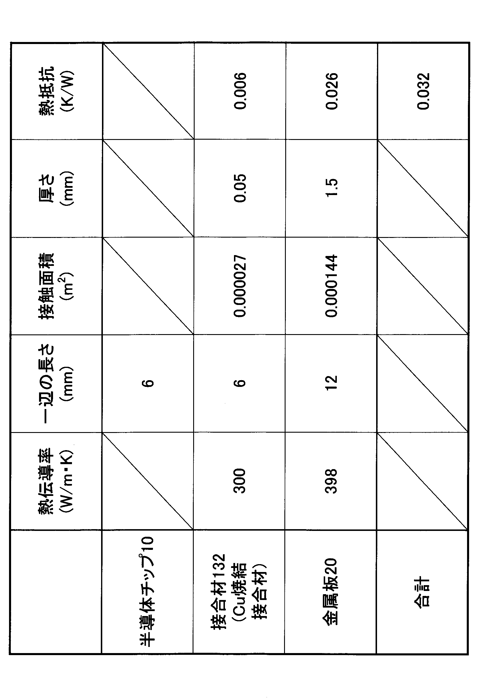
- Table 3 shows the results of simulation using the silicon carbide semiconductor device of the present embodiment shown in FIG. 6 as a model, and is a case where a Cu sintered bonding material is used as the second bonding material 132. It is the same as the case of Table 2 except that the thermal conductivity of the Cu sintered bonding material to be the bonding material is 300 W / m ⁇ K and the thickness is 0.05 mm. As a result, the thermal resistance of the second bonding material 132 is 0.006 K / W, and the thermal resistance of the metal plate 20 is 0.026 K / W. Therefore, the thermal resistance between the silicon carbide semiconductor chip 10 and the heat sink 50 Is 0.032 K / W. This value is about 2.6% of the thermal resistance in the silicon carbide semiconductor device having the structure shown in FIG. 3, and the thermal conductivity can be improved about 38 times.
- the silicon carbide semiconductor chip 10 is used as a MOSFET, and the gate electrode 11, the source electrode 12, and the drain electrode 13 are formed.
- the silicon carbide semiconductor chip 10 is formed of SiC. It may be another type of transistor.
- the first electrode of the silicon carbide semiconductor chip 10 serves as a gate electrode
- the second electrode serves as an emitter electrode
- the third electrode serves as a collector electrode.
- the gate electrode terminal 171 serves as a gate electrode terminal
- the source electrode terminal 172 serves as an emitter electrode terminal
- the drain electrode terminal 173 serves as a collector electrode terminal.
- Silicon Carbide Semiconductor Chip 10a First Surface 10b Second Surface 11 Gate Electrode (First Electrode) 12 Source electrode (second electrode) 13 Drain electrode (third electrode) 20 Metal plate 20a First main surface 20b Second main surface 31 Bonding material 40 Insulating sheet 50 Heat sink 120 Metal plate 120a First main surface 120b Second main surface 121 Insulating film 122 First conductive layer 131 First bonding material 132 Second Bonding Material 133 Third Bonding Material 160 Second Conductive Layer 171 Gate Electrode Terminal 172 Source Electrode Terminal 173 Drain Electrode Terminal 181 Bonding Wire 182 Bonding Wire 183 Bonding Wire 190 Mold Resin
Landscapes
- Cooling Or The Like Of Semiconductors Or Solid State Devices (AREA)
- Electrodes Of Semiconductors (AREA)
Abstract
炭化珪素半導体装置は、第1主面と、前記第1主面とは反対側に第2主面を有する金属板と、前記金属板の前記第1主面の一部に設けられた絶縁膜と、前記絶縁膜の上に設けられた第1の導電層と、第1面に第1の電極及び第2の電極を有し、前記第1面とは反対側の第2面に第3の電極を有する炭化珪素半導体チップと、を有し、前記炭化珪素半導体チップの前記第1面と前記金属板の前記第1主面とが対向して、前記第1の電極と前記第1の導電層とは第1の接合材により接合されており、前記第2の電極と前記金属板の前記第1主面とは第2の接合材により接合されている。
Description
本開示は、炭化珪素半導体装置に関する。
本出願は、2019年3月12日出願の日本出願第2019-045171号に基づく優先権を主張し、前記日本出願に記載された全ての記載内容を援用するものである。
MOSFET(metal-oxide-semiconductor field-effect transistor)等の炭化珪素半導体装置は、通常、半導体チップと電極端子とが接続されている状態でモールド樹脂等により固められている。半導体チップに用いられる半導体材料としては、シリコンが一般的であるが、耐圧の向上のため、Si(シリコン)よりもバンドギャップの広いSiC(炭化珪素)等を用い、厚さ方向に電流の流れる構造の縦型トランジスタがある。
本開示の炭化珪素半導体装置は、第1主面と、第1主面とは反対側に第2主面を有する金属板と、金属板の第1主面の一部に設けられた絶縁膜と、絶縁膜の上に設けられた第1の導電層と、第1面に第1の電極及び第2の電極を有する。また、第1面とは反対側の第2面に第3の電極を有する炭化珪素半導体チップと、を有する。更に、炭化珪素半導体チップの第1面と金属板の第1主面とが対向して、第1の電極と第1の導電層とは第1の接合材により接合されており、第2の電極と金属板の第1主面とは第2の接合材により接合されている。
[本開示が解決しようとする課題]
従来のSiCを用いた縦型トランジスタにすることにより、耐圧が向上し、大電流を流すことが可能となるが、半導体チップに大電流が流れると、発熱するため、効率よく放熱することが必要となる。
従来のSiCを用いた縦型トランジスタにすることにより、耐圧が向上し、大電流を流すことが可能となるが、半導体チップに大電流が流れると、発熱するため、効率よく放熱することが必要となる。
よって、SiCを用いた縦型トランジスタにおいて、効率よく放熱することのできる構造の炭化珪素半導体装置が求められている。
[本開示の効果]
本開示によれば、SiCを用いた縦型トランジスタにおいて、効率よく放熱できる構造の炭化珪素半導体装置を提供できる。
本開示によれば、SiCを用いた縦型トランジスタにおいて、効率よく放熱できる構造の炭化珪素半導体装置を提供できる。
実施するための形態について、以下に説明する。
[本開示の実施形態の説明]
最初に本開示の実施態様を列記して説明する。以下の説明では、同一または対応する要素には同一の符号を付し、それらについて同じ説明は繰り返さない。
最初に本開示の実施態様を列記して説明する。以下の説明では、同一または対応する要素には同一の符号を付し、それらについて同じ説明は繰り返さない。
〔1〕 本開示の一態様に係る炭化珪素半導体装置は、第1主面と、前記第1主面とは反対側に第2主面を有する金属板と、前記金属板の前記第1主面の一部に設けられた絶縁膜と、前記絶縁膜の上に設けられた第1の導電層と、第1面に第1の電極及び第2の電極を有し、前記第1面とは反対側の第2面に第3の電極を有する炭化珪素半導体チップと、を有し、前記炭化珪素半導体チップの前記第1面と前記金属板の前記第1主面とが対向して、前記第1の電極と前記第1の導電層とは第1の接合材により接合されており、前記第2の電極と前記金属板の前記第1主面とは第2の接合材により接合されている。
炭化珪素を用いた縦型トランジスタでは、大電流を流すことが可能である。しかしながら、縦型トランジスタが形成されている半導体チップに大電流を流すと発熱し、効率よく放熱することができないと、半導体チップの温度が上昇するため、特性が低下してしまう。一般的な炭化珪素を用いた縦型トランジスタでは、リードフレームに半導体チップのドレイン電極が接合されており、リードフレームの反対側の面には、絶縁シートを介し、ヒートシンクが接続されている。このような構造の場合、絶縁シートの熱伝導率は極めて低いことから、半導体チップにおいて生じた熱をヒートシンクに効率よく伝えることができないため、放熱が効率よくなされない。
このため、本願発明者は、縦型トランジスタにおいて生じた熱を効率よくヒートシンクに伝える方法について検討を行った。この結果、半導体チップのソース電極が形成されている面をリードフレームに直接接続することにより、リードフレームの反対側の面に、絶縁シート等を設けることなく、ヒートシンクを接続することができることを見出した。これにより、半導体チップとヒートシンクとの間の熱抵抗を低くし、半導体チップにおいて生じた熱を効率よくヒートシンクに伝え、放熱することが可能となる。
〔2〕 前記炭化珪素半導体チップの前記第3の電極の上に、第3の接合材により接合された第2の導電層を有してもよい。この場合、第2の導電層に電極端子を接続できる。
〔3〕 前記第1の電極は、ゲート電極であり、前記第2の電極は、ソース電極であり、前記第3の電極は、ドレイン電極であり、前記ゲート電極と、ゲート電極端子とは、ボンディングワイヤにより接続されており、前記ソース電極と、ソース電極端子とは、ボンディングワイヤにより接続されており、前記ドレイン電極と、ドレイン電極端子とは、ボンディングワイヤにより接続されていてもよい。この場合、例えば電界効果トランジスタを構成できる。
〔4〕 前記第1の電極は、ゲート電極であり、前記第2の電極は、エミッタ電極であり、前記第3の電極は、コレクタ電極であり、前記ゲート電極と、ゲート電極端子とは、ボンディングワイヤにより接続されており、前記エミッタ電極と、エミッタ電極端子とは、ボンディングワイヤにより接続されており、前記コレクタ電極と、コレクタ電極端子とは、ボンディングワイヤにより接続されていてもよい。この場合、例えば絶縁ゲートバイポーラトランジスタ(insulated gate bipolar transistor:IGBT)を構成できる。
〔5〕 前記第1の電極は、ゲート電極であり、前記第2の電極は、ソース電極であり、前記第3の電極は、ドレイン電極であり、前記ゲート電極と、ゲート電極端子とは、ボンディングワイヤにより接続されており、前記ソース電極と、ソース電極端子とは、ボンディングワイヤにより接続されており、前記第2の導電層と、ドレイン電極端子とは、ボンディングワイヤにより接続されていてもよい。この場合、例えば電界効果トランジスタを構成できる。
〔6〕 前記第1の電極は、ゲート電極であり、前記第2の電極は、エミッタ電極であり、前記第3の電極は、コレクタ電極であり、前記ゲート電極と、ゲート電極端子とは、ボンディングワイヤにより接続されており、前記エミッタ電極と、エミッタ電極端子とは、ボンディングワイヤにより接続されており、前記第2の導電層と、コレクタ電極端子とは、ボンディングワイヤにより接続されていてもよい。この場合、例えばIGBTを構成できる。
〔7〕 前記金属板は、熱伝導率が10W/m・K以上であり、線膨張係数は17.0ppm/K以下であり、体積抵抗率1μΩ・m以下であってもよい。この場合、熱抵抗を低くしやすく、剥離を生じにくくしやすい。
〔8〕 前記絶縁膜の膜厚は、10μm以上、40μm以下であってもよい。この場合、絶縁性を確保しながら、第1主面との間の段差を小さくしやすい。
〔9〕 前記第1の導電層の膜厚は、5μm以上、20μm以下であってもよい。この場合、導電性を確保しながら、第1主面との間の段差を小さくしやすい。
〔10〕 前記第1の接合材及び前記第2の接合材は、銅または銀を含んでもよい。この場合、熱抵抗を更に低くしやすい。
〔11〕 前記金属板の前記第2主面には、ヒートシンクが接続されていてもよい。この場合、放熱性を更に向上できる。
〔12〕 本開示の他の一態様に係る炭化珪素半導体装置は、第1主面と、前記第1主面とは反対側に第2主面を有する金属板と、前記金属板の前記第1主面の一部に設けられた絶縁膜と、前記絶縁膜の上に設けられた第1の導電層と、第1面に第1の電極及び第2の電極を有し、前記第1面とは反対側の第2面に第3の電極を有する炭化珪素半導体チップと、前記炭化珪素半導体チップの前記第3の電極の上に、第3の接合材により接合された第2の導電層と、を有し、前記炭化珪素半導体チップの前記第1面と前記金属板の前記第1主面とが対向して、前記第1の電極と前記第1の導電層とは第1の接合材により接合されており、前記第2の電極と前記金属板の前記第1主面とは第2の接合材により接合されており、前記金属板は、熱伝導率が10W/m・K以上であり、線膨張係数は17.0ppm/K以下であり、体積抵抗率1μΩ・m以下であり、前記絶縁膜の膜厚は、10μm以上、40μm以下であり、前記第1の導電層の膜厚は、5μm以上、20μm以下であり、前記第1の接合材及び前記第2の接合材は、銅または銀を含む。
[本開示の実施形態の詳細]
以下、本開示の一実施形態(以下「本実施形態」と記す)について詳細に説明するが、本実施形態はこれらに限定されるものではない。また、図面における長さや大きさ等は、説明のための便宜上、実際のものとは異なる場合がある。
以下、本開示の一実施形態(以下「本実施形態」と記す)について詳細に説明するが、本実施形態はこれらに限定されるものではない。また、図面における長さや大きさ等は、説明のための便宜上、実際のものとは異なる場合がある。
本実施形態で用いられる半導体チップは、SiC基板に縦型トランジスタが形成されている構造のものである。具体的には、図1に示されるように、炭化珪素半導体チップ10の一方の面となる第1面10aには、ゲート電極11及びソース電極12が形成されており、第1面10aとは反対の他方の面となる第2面10bには、ドレイン電極13が形成されている。本願においては、ゲート電極11を第1の電極と記載し、ソース電極12を第2の電極と記載し、ドレイン電極13を第3の電極と記載する場合がある。
次に、リードフレームの一部となる金属板の上に、炭化珪素半導体チップ10のドレイン電極13側を搭載した構造の炭化珪素半導体装置について、図3に基づき説明する。
図3に示される構造の炭化珪素半導体装置は、リードフレームの一部である金属板20の一方の面となる第1主面20aに、炭化珪素半導体チップ10のドレイン電極13が、Sn-Cuハンダ等の接合材31により接合されている。また、金属板20の第1主面20aとは反対の他方の面となる第2主面20bには、絶縁シート40を介し、ヒートシンク50が取り付けられている。
炭化珪素半導体チップ10は、SiCの縦型トランジスタであるため、高耐圧であって、大電流を流すことが可能であるが、炭化珪素半導体チップ10に大電流が流れると発熱する。半導体デバイスは、温度により特性が変化することから、炭化珪素半導体チップ10が高温になることは好ましくない。このため、図3に示されるように、金属板20の側に放熱のためヒートシンク50が設けられている。しかしながら、ドレイン電極13には高電圧が印加されるため、Al(アルミニウム)やCu(銅)等により形成されているヒートシンク50を金属板20に直接接続すると、ヒートシンク50も高電圧となってしまう。このため、金属板20の第2主面20bとヒートシンク50との間に絶縁シート40を設け、金属板20とヒートシンク50との間の絶縁がとられている。
しかしながら、金属板20とヒートシンク50との間に、絶縁シート40を設けた場合、絶縁シート40を形成している絶縁体は、極めて熱伝導率が低いことから、炭化珪素半導体チップ10において発生した熱を効率よくヒートシンク50に伝えることができない。即ち、炭化珪素半導体チップ10において発生した熱は、金属板20に伝導するが、金属板20とヒートシンク50との間に設けられた絶縁シート40は熱抵抗が高く、熱伝導が妨げられる。よって、炭化珪素半導体チップ10が高温となってしまう。
このため、絶縁シート40の厚さを薄くして、熱抵抗を減らす方法が考えられる。しかしながら、ドレイン電極13に印加される電圧は高電圧であるため、絶縁シート40の厚さを薄くしすぎると、高電圧が印加された際に破壊される場合がある。よって、絶縁シート40は、所定の厚さ以上の厚さが必要であることから、絶縁シート40の厚さを薄くすることには限界がある。
また、他には、金属板20の第2主面20bに面積の大きな熱拡散板を設け、熱拡散板、絶縁シート40を介し、ヒートシンク50に熱を伝える方法が考えられる。しかしながら、この場合には、熱拡散板の大きさに対応して、絶縁シート40やヒートシンク50を大きくする必要があるため、炭化珪素半導体装置が大型化してしまう。
(炭化珪素半導体装置)
次に、本実施形態における炭化珪素半導体装置について、図4~図6に基づき説明する。図4は、本実施形態における炭化珪素半導体装置の上面図であり、図5は斜視図であり、図6は要部の断面図である。
次に、本実施形態における炭化珪素半導体装置について、図4~図6に基づき説明する。図4は、本実施形態における炭化珪素半導体装置の上面図であり、図5は斜視図であり、図6は要部の断面図である。
本実施形態における炭化珪素半導体装置は、炭化珪素半導体チップ10のゲート電極11及びソース電極12が形成されている第1面10a側が、リードフレームの一部となる金属板120の一方の面となる第1主面120aに、接合材により接合されている。また、金属板120の第1主面120aとは反対側の他方の面となる第2主面120bには、ヒートシンク50が接続されている。従って、炭化珪素半導体チップ10とヒートシンク50との間には絶縁シート等の熱伝導を遮る部材は設けられていないため、炭化珪素半導体チップ10において発生した熱を金属板120を介しヒートシンク50に効率よく伝導させることができる。
本実施の形態においては、金属板120は、熱伝導率が10W/m・K以上であり、線膨張係数は17.0ppm/K以下であり、体積抵抗率1μΩ・m以下であることが好ましい。熱伝導率は150W/m・K以上であることがより好ましい。線膨張係数は7.5ppm/K以下であることがより好ましい。体積抵抗率は5.7×10-8Ω・m以下であることがより好ましい。炭化珪素半導体チップ10とヒートシンク50との間の熱抵抗を低くするためには、金属板120の熱伝導率は高い方が好ましい。また、金属板120の線膨張係数と炭化珪素半導体チップ10を形成しているSiCの熱膨張係数4.0ppm/Kとの差が大きいと、金属板120と炭化珪素半導体チップ10との間で剥離等が生じる場合がある。よって、金属板120の線膨張係数は、炭化珪素半導体チップ10を形成しているSiCの熱膨張係数4.0ppm/Kに近い値であることが好ましい。また、金属板120は、炭化珪素半導体チップ10のソース電極12と接続され、ソース配線の一部となるため、低抵抗、即ち、体積抵抗率が低い方が好ましい。
具体的には、本実施形態における炭化珪素半導体装置は、金属板120の第1主面120aの炭化珪素半導体チップ10のゲート電極11と接続される領域には、絶縁膜121が設けられており、絶縁膜121の上には、第1の導電層122が形成されている。金属板120は、銅、鉄ニッケル(Fe-Ni)合金、銅タングステン合金(Cu-W合金)、モリブデン、銅/鉄ニッケル合金/銅が厚み方向に積層された積層材等により形成されており、導電性を有している。絶縁膜121は、絶縁体材料、例えば、ポリイミド等により形成されており、第1の導電層122は、Cu等の導電材料により形成されている。
本実施形態においては、炭化珪素半導体チップ10の第1面10aと、金属板120の第1主面120aとが対向して接合されている。即ち、ゲート電極11は、金属板120に設けられた第1の導電層122に、第1の接合材131により接合されており、炭化珪素半導体チップ10のソース電極12は、金属板120の第1主面120aに、第2の接合材132により接合されている。
炭化珪素半導体チップ10の第2面10bのドレイン電極13は、第3の接合材133により、第2の導電層160が接合されている。第2の導電層160は、Cu等により形成されており、例えば、厚さが50μm~100μmの金属膜であってもよく、厚さが約1.5mmの金属板であってもよい。第2の導電層160は、炭化珪素半導体チップ10のドレイン電極13の厚さが薄いと、面内方向における抵抗が高くなることから、面内方向における抵抗を低くするために設けられている。従って、炭化珪素半導体チップ10のドレイン電極13が厚く、面内方向における抵抗が十分低い場合には、第2の導電層160を設ける必要はなく、炭化珪素半導体チップ10のドレイン電極13に直接ボンディングワイヤ183を接続してもよい。第1の接合材131、第2の接合材132、第3の接合材133は、Sn-Cuハンダ等により形成されているが、熱伝導率の高いCuを含む銅焼結接合材や、Ag(銀)を含む銀焼結接合材を用いることにより、より一層熱抵抗を低くすることができる。
本実施の形態においては、第1の導電層122は、ゲート電極端子171とボンディングワイヤ181により接続されている。金属板120の第1主面120aは、ソース電極端子172とボンディングワイヤ182により接続されている。第2の導電層160は、ドレイン電極端子173とボンディングワイヤ183により接続されている。
炭化珪素半導体チップ10においては、ドレイン電極13に印加される電圧と比べて、ソース電極12に印加される電圧は、ゲート電極11に印加される電圧に比較的近い電圧である。従って、金属板120の第1主面120aに形成される絶縁膜121の膜厚を薄くすることが可能であり、膜厚は、10μm以上、40μm以下が好ましい。また、第1の導電層122の膜厚は、5μm以上、20μm以下が好ましい。絶縁膜121及び第1の導電層122は薄い方が、金属板120の第1主面120aとの段差が小さくなるため、炭化珪素半導体チップ10の第1面10aと第1の接合材131及び第2の接合材132により接合する際に接合がしやすくなる。一方、絶縁膜121の膜厚が薄すぎると絶縁性が低下する。また、第1の導電層122が薄すぎると導電性が低下する。従って、絶縁膜121及び第1の導電層122の膜厚は、上記範囲であることが好ましい。
ところで、炭化珪素半導体チップ10の第1面10aに形成されるゲート電極11の面積は、ソース電極12の面積と比べて極めて小さい。これは、ソース電極12は電流を流すため、面積が広い方が好ましいが、ゲート電極11は制御のための電極であるため、面積が狭くても特性上問題が生じることはないからである。
本実施形態においては、炭化珪素半導体チップ10において生じた熱は、ソース電極12及び第2の接合材132を介し、金属板120に伝導し、更に、金属板120の第2主面120bに接続されているヒートシンク50に伝導し放熱される。よって、炭化珪素半導体チップ10とヒートシンク50との間には、熱伝導の障害となる絶縁シート等が存在していないため、効率よくヒートシンク50に熱を伝えて、放熱することができる。
(炭化珪素半導体装置の製造方法)
次に、本実施形態における炭化珪素半導体装置の製造方法について、図7~図14に基づき説明する。
次に、本実施形態における炭化珪素半導体装置の製造方法について、図7~図14に基づき説明する。
最初に、図7及び図8に示されるように、金属板120、ゲート電極端子171、ソース電極端子172、ドレイン電極端子173が形成されているリードフレームを用意する。リードフレームは、Cu等により形成されている金属板を打ち抜き加工することにより形成されており、金属板120、ゲート電極端子171、ソース電極端子172、ドレイン電極端子173は、不図示のリードフレームの枠に接続されている。リードフレームの枠は半導体装置の製造工程の最後で切り取られるため、製造される半導体装置には枠が残ることはないことから、本実施形態における説明では、便宜上、リードフレームの枠を省略して説明する。尚、図7は、金属板120、ゲート電極端子171、ソース電極端子172、ドレイン電極端子173の上面図であり、図8は斜視図である。この後の工程の説明では、斜視図に基づき説明する。
次に、図9に示されるように、金属板120の第1主面120aの炭化珪素半導体チップ10のゲート電極11と接続される領域を含む領域に絶縁膜121を形成し、更に、絶縁膜121の上に第1の導電層122を形成する。絶縁膜121は、膜厚が約30μmのポリイミド等により形成し、第1の導電層122は、膜厚が5μm~20μmのCu膜により形成する。
次に、図10に示されるように、金属板120の第1主面120aと炭化珪素半導体チップ10の第1面10aとを対向させ、第1の接合材131及び第2の接合材132により接合する。具体的には、金属板120の第1主面120aに形成されている第1の導電層122と炭化珪素半導体チップ10の第1面10aのゲート電極11とを第1の接合材131により接合する。同時に、金属板120の第1主面120aと炭化珪素半導体チップ10の第1面10aのソース電極12とを第2の接合材132により接合する。
具体的には、第1の接合材131及び第2の接合材132を形成するための接合材を第1の導電層122及び金属板120に供給し、この接合材の上に炭化珪素半導体チップ10を載置し、加熱して接合材を溶融させる。これにより、溶融した接合材が流動し、第2の接合材132よりも第1の接合材131が薄くなり、この後、凝固させる。尚、絶縁膜121が露出しているゲート電極11とソース電極12との間の長さよりも、第1の接合材131及び第2の接合材132の厚さは十分薄く、溶融した状態の接合材は、絶縁膜121の上ではじかれる。よって、第1の接合材131と第2の接合材132とは分離して形成される。
次に、図11に示されるように、炭化珪素半導体チップ10の第2面10bのドレイン電極13に、第2の導電層160を第3の接合材133により接合する。
次に、図12に示されるように、ワイヤボンディングにより、ゲート電極端子171、ソース電極端子172、ドレイン電極端子173を接続する。具体的には、金属板120の第1主面120aに形成された第1の導電層122とゲート電極端子171とをボンディングワイヤ181により接続する。炭化珪素半導体チップ10のゲート電極11は、第1の接合材131により第1の導電層122と接続されているため、ボンディングワイヤ181の接続により、炭化珪素半導体チップ10のゲート電極11とゲート電極端子171とが電気的に接続される。
同様に、金属板120の第1主面120aとソース電極端子172とをボンディングワイヤ182により接続する。炭化珪素半導体チップ10のソース電極12は、第2の接合材132により金属板120の第1主面120aと接続されているため、ボンディングワイヤ182の接続により、炭化珪素半導体チップ10のソース電極12とソース電極端子172とが電気的に接続される。
同様に、炭化珪素半導体チップ10の第2面10bの上の第2の導電層160とドレイン電極端子173とをボンディングワイヤ183により接続する。炭化珪素半導体チップ10のドレイン電極13は、第3の接合材133により第2の導電層160と接続されているため、ボンディングワイヤ183の接続により、炭化珪素半導体チップ10のドレイン電極13とドレイン電極端子173とが電気的に接続される。
次に、図13及び図14に示されるように、金属板120の第1主面120a、炭化珪素半導体チップ10、ゲート電極端子171の一部、ソース電極端子172の一部、ドレイン電極端子173の一部をトランスファモールド成形しモールド樹脂190により固める。これにより、金属板120の第1主面120a、炭化珪素半導体チップ10、ゲート電極端子171の一部、ソース電極端子172の一部、ドレイン電極端子173の一部がモールド樹脂190により覆われる。金属板120の第2主面120bは、モールド樹脂190により覆われることはなく、露出させる。これは、金属板120の第2主面120bを不図示のヒートシンクに接触させて放熱するためである。尚、図13は、金属板120の第1主面120a側の斜視図であり、図14は、第2主面120b側の斜視図である。
以上の工程により、本実施形態における炭化珪素半導体装置を製造することができる。
(シミュレーション)
次に、図3に示される炭化珪素半導体装置と、本実施形態における炭化珪素半導体装置とにおける放熱の効果を説明するために行ったシミュレーションについて説明する。シミュレーションでは、接合材となるSn-Cuハンダの熱伝導率を63W/m・Kとし、金属板20の熱伝導率を398W/m・Kとし、絶縁シート40の熱伝導率を12W/m・Kとした。これらの値より、炭化珪素半導体チップ10とヒートシンク50との間の熱抵抗を算出した。
次に、図3に示される炭化珪素半導体装置と、本実施形態における炭化珪素半導体装置とにおける放熱の効果を説明するために行ったシミュレーションについて説明する。シミュレーションでは、接合材となるSn-Cuハンダの熱伝導率を63W/m・Kとし、金属板20の熱伝導率を398W/m・Kとし、絶縁シート40の熱伝導率を12W/m・Kとした。これらの値より、炭化珪素半導体チップ10とヒートシンク50との間の熱抵抗を算出した。
表1は、図3に示される構造の炭化珪素半導体装置をモデルとしてシミュレーションを行った結果である。炭化珪素半導体チップ10は一辺の長さが6mmの略正方形とした。接合材31となるSn-Cuハンダは、炭化珪素半導体チップ10の第2面10bの全面で接しているものとし、一辺の長さが6mmの略正方形で、厚さを0.1mmとした。金属板20は一辺の長さが12mmの略正方形で、厚さを1.5mmとし、絶縁シート40は一辺の長さが12mmの略正方形で、厚さを2.0mmとした。この結果、接合材31の熱抵抗は0.044K/W、金属板20の熱抵抗は0.026K/W、絶縁シート40の熱抵抗は1.157K/Wとなるため、炭化珪素半導体チップ10とヒートシンク50との間の熱抵抗は1.228K/Wとなる。これら接合材31、金属板20及び絶縁シート40の熱抵抗の値は小数第4位を四捨五入して得られる値である。四捨五入をしていない熱抵抗の値の和をとり、その小数第4位を四捨五入すると、1.228K/Wが得られる。

表2は、図6に示される本実施形態の炭化珪素半導体装置をモデルとしてシミュレーションを行った結果である。炭化珪素半導体チップ10は一辺の長さが6mmの略正方形とした。第2の接合材132となるSn-Cuハンダは、炭化珪素半導体チップ10の第2面10bの3/4の面積で接しているものとし、厚さを0.1mmとした。金属板20は一辺の長さが12mmの略正方形で、厚さを1.5mmとした。この結果、第2の接合材132の熱抵抗は0.059K/Wとなり、金属板20の熱抵抗は0.026K/Wであるため、炭化珪素半導体チップ10とヒートシンク50との間の熱抵抗は0.085K/Wとなる。この値は、図3に示される構造の炭化珪素半導体装置における熱抵抗の約7%であり、熱伝導性を約14倍向上させることができる。尚、図3に示される炭化珪素半導体装置において、金属板20の第2主面20bに熱拡散板を用いて、同様の放熱をしようとした場合には、金属板20に対し約50倍の面積の熱拡散板を設けることが必要となり、半導体装置が大型化してしまう。
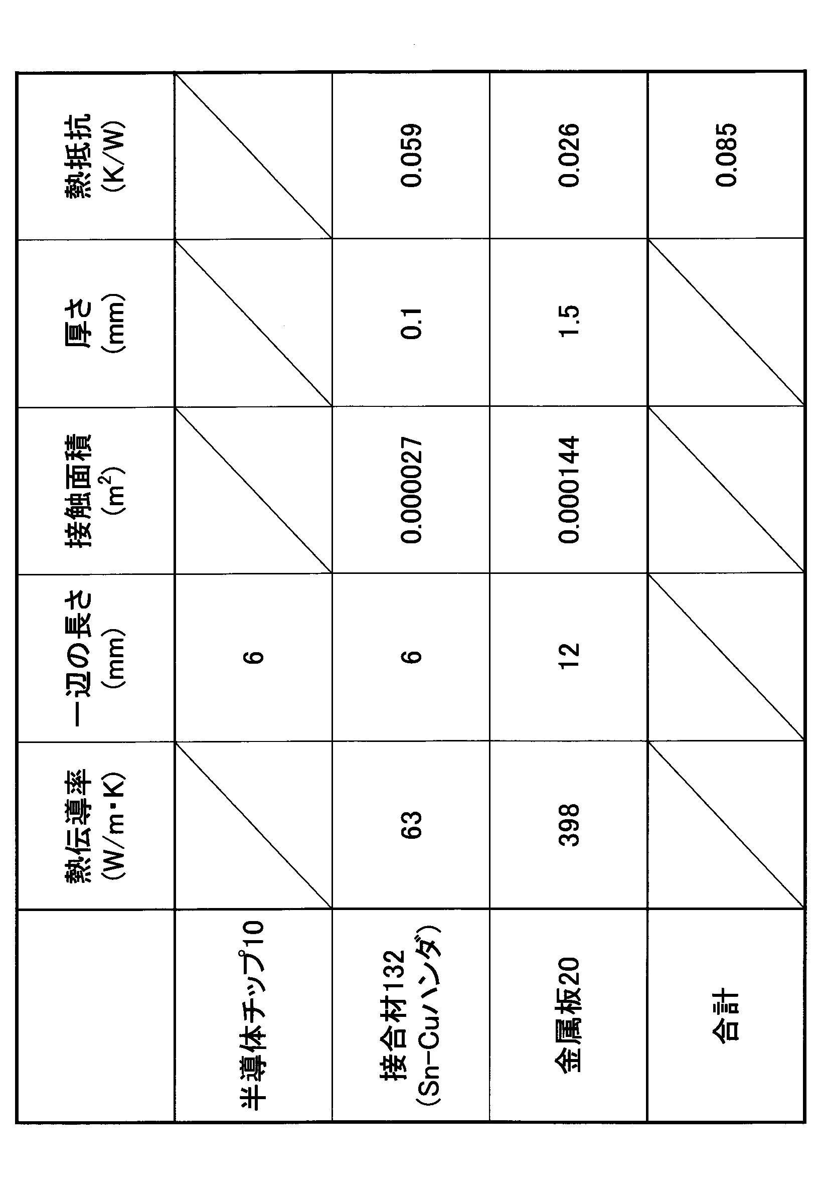
表3は、図6に示される本実施形態の炭化珪素半導体装置をモデルとしてシミュレーションを行った結果であり、第2の接合材132にCu焼結接合材を用いた場合である。接合材となるCu焼結接合材の熱伝導率を300W/m・Kとし、厚さを0.05mmとしたこと以外は、表2の場合と同じである。この結果、第2の接合材132の熱抵抗は0.006K/Wとなり、金属板20の熱抵抗は0.026K/Wであるため、炭化珪素半導体チップ10とヒートシンク50との間の熱抵抗は0.032K/Wとなる。この値は、図3に示される構造の炭化珪素半導体装置における熱抵抗の約2.6%であり、熱伝導性を約38倍向上させることができる。
尚、上記のおける説明では、炭化珪素半導体チップ10をMOSFETとし、ゲート電極11、ソース電極12、ドレイン電極13が形成されているものについて説明したが、炭化珪素半導体チップ10は、SiCにより形成された他の形式のトランジスタであってもよい。例えばIGBT(Insulated Gate Bipolar Transistor)の場合、炭化珪素半導体チップ10の第1の電極がゲート電極となり、第2の電極がエミッタ電極となり、第3の電極がコレクタ電極となる。また、ゲート電極端子171がゲート電極端子となり、ソース電極端子172がエミッタ電極端子となり、ドレイン電極端子173がコレクタ電極端子となる。
以上、実施形態について詳述したが、特定の実施形態に限定されるものではなく、請求の範囲に記載された範囲内において、種々の変形及び変更が可能である。
10 炭化珪素半導体チップ
10a 第1面
10b 第2面
11 ゲート電極(第1の電極)
12 ソース電極(第2の電極)
13 ドレイン電極(第3の電極)
20 金属板
20a 第1主面
20b 第2主面
31 接合材
40 絶縁シート
50 ヒートシンク
120 金属板
120a 第1主面
120b 第2主面
121 絶縁膜
122 第1の導電層
131 第1の接合材
132 第2の接合材
133 第3の接合材
160 第2の導電層
171 ゲート電極端子
172 ソース電極端子
173 ドレイン電極端子
181 ボンディングワイヤ
182 ボンディングワイヤ
183 ボンディングワイヤ
190 モールド樹脂
10a 第1面
10b 第2面
11 ゲート電極(第1の電極)
12 ソース電極(第2の電極)
13 ドレイン電極(第3の電極)
20 金属板
20a 第1主面
20b 第2主面
31 接合材
40 絶縁シート
50 ヒートシンク
120 金属板
120a 第1主面
120b 第2主面
121 絶縁膜
122 第1の導電層
131 第1の接合材
132 第2の接合材
133 第3の接合材
160 第2の導電層
171 ゲート電極端子
172 ソース電極端子
173 ドレイン電極端子
181 ボンディングワイヤ
182 ボンディングワイヤ
183 ボンディングワイヤ
190 モールド樹脂
Claims (12)
- 第1主面と、前記第1主面とは反対側に第2主面を有する金属板と、
前記金属板の前記第1主面の一部に設けられた絶縁膜と、
前記絶縁膜の上に設けられた第1の導電層と、
第1面に第1の電極及び第2の電極を有し、前記第1面とは反対側の第2面に第3の電極を有する炭化珪素半導体チップと、
を有し、
前記炭化珪素半導体チップの前記第1面と前記金属板の前記第1主面とが対向して、前記第1の電極と前記第1の導電層とは第1の接合材により接合されており、前記第2の電極と前記金属板の前記第1主面とは第2の接合材により接合されている炭化珪素半導体装置。 - 前記炭化珪素半導体チップの前記第3の電極の上に、第3の接合材により接合された第2の導電層を有する請求項1に記載の炭化珪素半導体装置。
- 前記第1の電極は、ゲート電極であり、
前記第2の電極は、ソース電極であり、
前記第3の電極は、ドレイン電極であり、
前記ゲート電極と、ゲート電極端子とは、ボンディングワイヤにより接続されており、
前記ソース電極と、ソース電極端子とは、ボンディングワイヤにより接続されており、
前記ドレイン電極と、ドレイン電極端子とは、ボンディングワイヤにより接続されている請求項1に記載の炭化珪素半導体装置。 - 前記第1の電極は、ゲート電極であり、
前記第2の電極は、エミッタ電極であり、
前記第3の電極は、コレクタ電極であり、
前記ゲート電極と、ゲート電極端子とは、ボンディングワイヤにより接続されており、
前記エミッタ電極と、エミッタ電極端子とは、ボンディングワイヤにより接続されており、
前記コレクタ電極と、コレクタ電極端子とは、ボンディングワイヤにより接続されている請求項1に記載の炭化珪素半導体装置。 - 前記第1の電極は、ゲート電極であり、
前記第2の電極は、ソース電極であり、
前記第3の電極は、ドレイン電極であり、
前記ゲート電極と、ゲート電極端子とは、ボンディングワイヤにより接続されており、
前記ソース電極と、ソース電極端子とは、ボンディングワイヤにより接続されており、
前記第2の導電層と、ドレイン電極端子とは、ボンディングワイヤにより接続されている請求項2に記載の炭化珪素半導体装置。 - 前記第1の電極は、ゲート電極であり、
前記第2の電極は、エミッタ電極であり、
前記第3の電極は、コレクタ電極であり、
前記ゲート電極と、ゲート電極端子とは、ボンディングワイヤにより接続されており、
前記エミッタ電極と、エミッタ電極端子とは、ボンディングワイヤにより接続されており、
前記第2の導電層と、コレクタ電極端子とは、ボンディングワイヤにより接続されている請求項2に記載の炭化珪素半導体装置。 - 前記金属板は、熱伝導率が10W/m・K以上であり、線膨張係数は17.0ppm/K以下であり、体積抵抗率1μΩ・m以下である請求項1から請求項6のいずれか一項に記載の炭化珪素半導体装置。
- 前記絶縁膜の膜厚は、10μm以上、40μm以下である請求項1から請求項7のいずれか一項に記載の炭化珪素半導体装置。
- 前記第1の導電層の膜厚は、5μm以上、20μm以下である請求項1から請求項8のいずれか一項に記載の炭化珪素半導体装置。
- 前記第1の接合材及び前記第2の接合材は、銅または銀を含む請求項1から請求項9のいずれか一項に記載の炭化珪素半導体装置。
- 前記金属板の前記第2主面には、ヒートシンクが接続されている請求項1から請求項10のいずれか一項に記載の炭化珪素半導体装置。
- 第1主面と、前記第1主面とは反対側に第2主面を有する金属板と、
前記金属板の前記第1主面の一部に設けられた絶縁膜と、
前記絶縁膜の上に設けられた第1の導電層と、
第1面に第1の電極及び第2の電極を有し、前記第1面とは反対側の第2面に第3の電極を有する炭化珪素半導体チップと、
前記炭化珪素半導体チップの前記第3の電極の上に、第3の接合材により接合された第2の導電層と、
を有し、
前記炭化珪素半導体チップの前記第1面と前記金属板の前記第1主面とが対向して、前記第1の電極と前記第1の導電層とは第1の接合材により接合されており、前記第2の電極と前記金属板の前記第1主面とは第2の接合材により接合されており、
前記金属板は、熱伝導率が10W/m・K以上であり、線膨張係数は17.0ppm/K以下であり、体積抵抗率1μΩ・m以下であり、
前記絶縁膜の膜厚は、10μm以上、40μm以下であり、
前記第1の導電層の膜厚は、5μm以上、20μm以下であり、
前記第1の接合材及び前記第2の接合材は、銅または銀を含む炭化珪素半導体装置。
Priority Applications (2)
| Application Number | Priority Date | Filing Date | Title |
|---|---|---|---|
| JP2021504956A JP7298679B2 (ja) | 2019-03-12 | 2020-03-03 | 炭化珪素半導体装置 |
| US17/311,000 US11715767B2 (en) | 2019-03-12 | 2020-03-03 | Silicon carbide semiconductor device |
Applications Claiming Priority (2)
| Application Number | Priority Date | Filing Date | Title |
|---|---|---|---|
| JP2019-045171 | 2019-03-12 | ||
| JP2019045171 | 2019-03-12 |
Publications (1)
| Publication Number | Publication Date |
|---|---|
| WO2020184304A1 true WO2020184304A1 (ja) | 2020-09-17 |
Family
ID=72426376
Family Applications (1)
| Application Number | Title | Priority Date | Filing Date |
|---|---|---|---|
| PCT/JP2020/008952 Ceased WO2020184304A1 (ja) | 2019-03-12 | 2020-03-03 | 炭化珪素半導体装置 |
Country Status (3)
| Country | Link |
|---|---|
| US (1) | US11715767B2 (ja) |
| JP (1) | JP7298679B2 (ja) |
| WO (1) | WO2020184304A1 (ja) |
Families Citing this family (1)
| Publication number | Priority date | Publication date | Assignee | Title |
|---|---|---|---|---|
| KR20230095546A (ko) * | 2021-12-22 | 2023-06-29 | 주식회사 엘엑스세미콘 | 전력반도체모듈 및 그 제조방법 |
Citations (4)
| Publication number | Priority date | Publication date | Assignee | Title |
|---|---|---|---|---|
| JP2006179735A (ja) * | 2004-12-24 | 2006-07-06 | Renesas Technology Corp | 半導体装置およびその製造方法 |
| WO2013061392A1 (ja) * | 2011-10-24 | 2013-05-02 | トヨタ自動車株式会社 | 半導体モジュール |
| JP2013089948A (ja) * | 2011-10-18 | 2013-05-13 | Rohm Co Ltd | 半導体装置およびその製造方法 |
| JP2017034161A (ja) * | 2015-08-04 | 2017-02-09 | 株式会社デンソー | 電子装置の製造方法 |
Family Cites Families (2)
| Publication number | Priority date | Publication date | Assignee | Title |
|---|---|---|---|---|
| JP4228926B2 (ja) | 2003-10-03 | 2009-02-25 | 富士電機デバイステクノロジー株式会社 | 半導体装置 |
| JP5542567B2 (ja) | 2010-07-27 | 2014-07-09 | 三菱電機株式会社 | 半導体装置 |
-
2020
- 2020-03-03 US US17/311,000 patent/US11715767B2/en active Active
- 2020-03-03 WO PCT/JP2020/008952 patent/WO2020184304A1/ja not_active Ceased
- 2020-03-03 JP JP2021504956A patent/JP7298679B2/ja active Active
Patent Citations (4)
| Publication number | Priority date | Publication date | Assignee | Title |
|---|---|---|---|---|
| JP2006179735A (ja) * | 2004-12-24 | 2006-07-06 | Renesas Technology Corp | 半導体装置およびその製造方法 |
| JP2013089948A (ja) * | 2011-10-18 | 2013-05-13 | Rohm Co Ltd | 半導体装置およびその製造方法 |
| WO2013061392A1 (ja) * | 2011-10-24 | 2013-05-02 | トヨタ自動車株式会社 | 半導体モジュール |
| JP2017034161A (ja) * | 2015-08-04 | 2017-02-09 | 株式会社デンソー | 電子装置の製造方法 |
Also Published As
| Publication number | Publication date |
|---|---|
| US11715767B2 (en) | 2023-08-01 |
| JPWO2020184304A1 (ja) | 2020-09-17 |
| US20220165851A1 (en) | 2022-05-26 |
| JP7298679B2 (ja) | 2023-06-27 |
Similar Documents
| Publication | Publication Date | Title |
|---|---|---|
| KR100957078B1 (ko) | 전기적으로 절연된 전력 장치 패키지 | |
| CN102593081B (zh) | 包括散热器的半导体器件 | |
| TWI446493B (zh) | 包括堆疊晶粒及散熱件結構之半導體晶粒封裝體 | |
| CN101577237B (zh) | 包括第一和第二支座的半导体装置和方法 | |
| US11972997B2 (en) | Semiconductor device | |
| CN101073151B (zh) | 具有增强散热性的半导体封装结构 | |
| WO2018135239A1 (ja) | 半導体装置および電力変換装置 | |
| JP2019186326A (ja) | 半導体装置およびその製造方法 | |
| CN111354710B (zh) | 半导体装置及其制造方法 | |
| CN111293095A (zh) | 半导体装置及其制造方法 | |
| US20140374926A1 (en) | Semiconductor device | |
| CN112071816A (zh) | 半导体封装和制造半导体封装的方法 | |
| JP7298679B2 (ja) | 炭化珪素半導体装置 | |
| CN108701671A (zh) | 制造电路载体的方法、电路载体、制造半导体模块的方法和半导体模块 | |
| CN115810603A (zh) | 半导体装置 | |
| JP7495225B2 (ja) | 半導体装置 | |
| CN111433910A (zh) | 半导体装置以及半导体装置的制造方法 | |
| CN101819955B (zh) | 具有增强散热性的半导体封装结构 | |
| JP2015167171A (ja) | 半導体装置 | |
| JP6317178B2 (ja) | 回路基板および電子装置 | |
| JP7294403B2 (ja) | 半導体装置 | |
| CN111584422A (zh) | 半导体装置及其制造方法 | |
| CN208240667U (zh) | 半导体封装结构 | |
| JP7802763B2 (ja) | 半導体装置 | |
| TWI823480B (zh) | 半導體裝置 |
Legal Events
| Date | Code | Title | Description |
|---|---|---|---|
| 121 | Ep: the epo has been informed by wipo that ep was designated in this application |
Ref document number: 20769785 Country of ref document: EP Kind code of ref document: A1 |
|
| ENP | Entry into the national phase |
Ref document number: 2021504956 Country of ref document: JP Kind code of ref document: A |
|
| NENP | Non-entry into the national phase |
Ref country code: DE |
|
| 122 | Ep: pct application non-entry in european phase |
Ref document number: 20769785 Country of ref document: EP Kind code of ref document: A1 |