WO2020179463A1 - マスクブランク、転写用マスクの製造方法、及び半導体デバイスの製造方法 - Google Patents
マスクブランク、転写用マスクの製造方法、及び半導体デバイスの製造方法 Download PDFInfo
- Publication number
- WO2020179463A1 WO2020179463A1 PCT/JP2020/006731 JP2020006731W WO2020179463A1 WO 2020179463 A1 WO2020179463 A1 WO 2020179463A1 JP 2020006731 W JP2020006731 W JP 2020006731W WO 2020179463 A1 WO2020179463 A1 WO 2020179463A1
- Authority
- WO
- WIPO (PCT)
- Prior art keywords
- film
- pattern
- mask
- hard mask
- etching
- Prior art date
- Legal status (The legal status is an assumption and is not a legal conclusion. Google has not performed a legal analysis and makes no representation as to the accuracy of the status listed.)
- Ceased
Links
Images




Classifications
-
- G—PHYSICS
- G03—PHOTOGRAPHY; CINEMATOGRAPHY; ANALOGOUS TECHNIQUES USING WAVES OTHER THAN OPTICAL WAVES; ELECTROGRAPHY; HOLOGRAPHY
- G03F—PHOTOMECHANICAL PRODUCTION OF TEXTURED OR PATTERNED SURFACES, e.g. FOR PRINTING, FOR PROCESSING OF SEMICONDUCTOR DEVICES; MATERIALS THEREFOR; ORIGINALS THEREFOR; APPARATUS SPECIALLY ADAPTED THEREFOR
- G03F1/00—Originals for photomechanical production of textured or patterned surfaces, e.g., masks, photo-masks, reticles; Mask blanks or pellicles therefor; Containers specially adapted therefor; Preparation thereof
- G03F1/26—Phase shift masks [PSM]; PSM blanks; Preparation thereof
- G03F1/32—Attenuating PSM [att-PSM], e.g. halftone PSM or PSM having semi-transparent phase shift portion; Preparation thereof
-
- G—PHYSICS
- G03—PHOTOGRAPHY; CINEMATOGRAPHY; ANALOGOUS TECHNIQUES USING WAVES OTHER THAN OPTICAL WAVES; ELECTROGRAPHY; HOLOGRAPHY
- G03F—PHOTOMECHANICAL PRODUCTION OF TEXTURED OR PATTERNED SURFACES, e.g. FOR PRINTING, FOR PROCESSING OF SEMICONDUCTOR DEVICES; MATERIALS THEREFOR; ORIGINALS THEREFOR; APPARATUS SPECIALLY ADAPTED THEREFOR
- G03F1/00—Originals for photomechanical production of textured or patterned surfaces, e.g., masks, photo-masks, reticles; Mask blanks or pellicles therefor; Containers specially adapted therefor; Preparation thereof
- G03F1/22—Masks or mask blanks for imaging by radiation of 100nm or shorter wavelength, e.g. X-ray masks, extreme ultraviolet [EUV] masks; Preparation thereof
- G03F1/24—Reflection masks; Preparation thereof
-
- G—PHYSICS
- G03—PHOTOGRAPHY; CINEMATOGRAPHY; ANALOGOUS TECHNIQUES USING WAVES OTHER THAN OPTICAL WAVES; ELECTROGRAPHY; HOLOGRAPHY
- G03F—PHOTOMECHANICAL PRODUCTION OF TEXTURED OR PATTERNED SURFACES, e.g. FOR PRINTING, FOR PROCESSING OF SEMICONDUCTOR DEVICES; MATERIALS THEREFOR; ORIGINALS THEREFOR; APPARATUS SPECIALLY ADAPTED THEREFOR
- G03F1/00—Originals for photomechanical production of textured or patterned surfaces, e.g., masks, photo-masks, reticles; Mask blanks or pellicles therefor; Containers specially adapted therefor; Preparation thereof
- G03F1/26—Phase shift masks [PSM]; PSM blanks; Preparation thereof
-
- G—PHYSICS
- G03—PHOTOGRAPHY; CINEMATOGRAPHY; ANALOGOUS TECHNIQUES USING WAVES OTHER THAN OPTICAL WAVES; ELECTROGRAPHY; HOLOGRAPHY
- G03F—PHOTOMECHANICAL PRODUCTION OF TEXTURED OR PATTERNED SURFACES, e.g. FOR PRINTING, FOR PROCESSING OF SEMICONDUCTOR DEVICES; MATERIALS THEREFOR; ORIGINALS THEREFOR; APPARATUS SPECIALLY ADAPTED THEREFOR
- G03F1/00—Originals for photomechanical production of textured or patterned surfaces, e.g., masks, photo-masks, reticles; Mask blanks or pellicles therefor; Containers specially adapted therefor; Preparation thereof
- G03F1/38—Masks having auxiliary features, e.g. special coatings or marks for alignment or testing; Preparation thereof
-
- G—PHYSICS
- G03—PHOTOGRAPHY; CINEMATOGRAPHY; ANALOGOUS TECHNIQUES USING WAVES OTHER THAN OPTICAL WAVES; ELECTROGRAPHY; HOLOGRAPHY
- G03F—PHOTOMECHANICAL PRODUCTION OF TEXTURED OR PATTERNED SURFACES, e.g. FOR PRINTING, FOR PROCESSING OF SEMICONDUCTOR DEVICES; MATERIALS THEREFOR; ORIGINALS THEREFOR; APPARATUS SPECIALLY ADAPTED THEREFOR
- G03F1/00—Originals for photomechanical production of textured or patterned surfaces, e.g., masks, photo-masks, reticles; Mask blanks or pellicles therefor; Containers specially adapted therefor; Preparation thereof
- G03F1/54—Absorbers, e.g. of opaque materials
-
- G—PHYSICS
- G03—PHOTOGRAPHY; CINEMATOGRAPHY; ANALOGOUS TECHNIQUES USING WAVES OTHER THAN OPTICAL WAVES; ELECTROGRAPHY; HOLOGRAPHY
- G03F—PHOTOMECHANICAL PRODUCTION OF TEXTURED OR PATTERNED SURFACES, e.g. FOR PRINTING, FOR PROCESSING OF SEMICONDUCTOR DEVICES; MATERIALS THEREFOR; ORIGINALS THEREFOR; APPARATUS SPECIALLY ADAPTED THEREFOR
- G03F1/00—Originals for photomechanical production of textured or patterned surfaces, e.g., masks, photo-masks, reticles; Mask blanks or pellicles therefor; Containers specially adapted therefor; Preparation thereof
- G03F1/68—Preparation processes not covered by groups G03F1/20 - G03F1/50
- G03F1/80—Etching
-
- G—PHYSICS
- G03—PHOTOGRAPHY; CINEMATOGRAPHY; ANALOGOUS TECHNIQUES USING WAVES OTHER THAN OPTICAL WAVES; ELECTROGRAPHY; HOLOGRAPHY
- G03F—PHOTOMECHANICAL PRODUCTION OF TEXTURED OR PATTERNED SURFACES, e.g. FOR PRINTING, FOR PROCESSING OF SEMICONDUCTOR DEVICES; MATERIALS THEREFOR; ORIGINALS THEREFOR; APPARATUS SPECIALLY ADAPTED THEREFOR
- G03F7/00—Photomechanical, e.g. photolithographic, production of textured or patterned surfaces, e.g. printing surfaces; Materials therefor, e.g. comprising photoresists; Apparatus specially adapted therefor
- G03F7/20—Exposure; Apparatus therefor
-
- H—ELECTRICITY
- H10—SEMICONDUCTOR DEVICES; ELECTRIC SOLID-STATE DEVICES NOT OTHERWISE PROVIDED FOR
- H10P—GENERIC PROCESSES OR APPARATUS FOR THE MANUFACTURE OR TREATMENT OF DEVICES COVERED BY CLASS H10
- H10P76/00—Manufacture or treatment of masks on semiconductor bodies, e.g. by lithography or photolithography
- H10P76/20—Manufacture or treatment of masks on semiconductor bodies, e.g. by lithography or photolithography of masks comprising organic materials
- H10P76/204—Manufacture or treatment of masks on semiconductor bodies, e.g. by lithography or photolithography of masks comprising organic materials of organic photoresist masks
- H10P76/2041—Photolithographic processes
Definitions
- the present invention relates to a mask blank, a method for manufacturing a transfer mask using this mask blank, and a method for manufacturing a semiconductor device using the transfer mask manufactured from this mask blank.
- a halftone phase shift film made of a metal silicide-based material, a light-shielding film made of a chromium-based material, and an etching mask film made of an inorganic material (hard mask film) on a translucent substrate As a mask blank for a halftone type phase shift mask, a halftone phase shift film made of a metal silicide-based material, a light-shielding film made of a chromium-based material, and an etching mask film made of an inorganic material (hard mask film) on a translucent substrate.
- a mask blank having a laminated structure is known (for example, see Patent Document 1).
- the etching mask film is patterned by dry etching with a fluorine-based gas using the resist pattern formed on the surface of the mask blank as a mask.
- the light shielding film is patterned by dry etching with a mixed gas of chlorine and oxygen using the etching mask film as a mask.
- the phase shift film is patterned by
- the light-shielding film made of a chromium-based compound is required to have a light-shielding performance of reducing the exposure light transmitted through the phase shift film to a predetermined amount or less.
- a phase shift mask is produced from this mask blank, a pattern including a light shielding band is formed on the light shielding film.
- the laminated structure of the phase shift film and the light-shielding film satisfies a predetermined optical density.
- the light-shielding film is required to function as an etching mask when the phase shift film is patterned by dry etching of a fluorine-based gas to form a phase shift pattern.
- a relatively sparse pattern such as a light shielding pattern is generally formed on the light shielding film.
- the light shielding film needs to function as an etching mask when forming a phase shift pattern which is a fine transfer pattern on the phase shift film. Therefore, it is desired that a fine pattern can be formed with high dimensional accuracy even in a light-shielding film.
- a mixed gas of chlorine-based gas and oxygen gas oxygen-containing chlorine-based gas
- oxygen-containing chlorine-based gas oxygen-containing chlorine-based gas
- dry etching using this oxygen-containing chlorine-based gas as an etching gas has a small tendency of anisotropic etching and a large tendency of isotropic etching.
- etching proceeds not only in the thickness direction of the film but also in the side wall direction of the pattern formed on the thin film, so-called side etching.
- side etching In order to suppress the progress of this side etching, a bias voltage is applied from the opposite side of the main surface of the substrate on which the thin film is formed during dry etching, and the etching gas comes into contact with more in the thickness direction of the film. It has been controlled in this way.
- ion-based dry etching which uses an etching gas that tends to become ionic plasma, such as a fluorine-based gas
- a bias voltage is high, and the etching anisotropy. Therefore, the amount of side etching of the thin film to be etched can be made very small.
- the resist pattern is etched from above and declines. At this time, the side wall direction of the resist pattern is also etched and reduced. Therefore, the width of the pattern formed on the resist film is designed in advance in consideration of the amount of decrease due to side etching. Further, the width of the pattern formed on the resist film is designed in consideration of the side etching amount of the light shielding film made of a chromium-based material.
- an etching mask film made of a material having sufficient etching selectivity with a chromium-based material against dry etching of oxygen-containing chlorine-based gas has been formed on a light-shielding film of a chromium-based material.
- the provided mask blank is beginning to be used.
- a pattern is formed on the hard mask film by dry etching using the resist pattern as a mask.
- dry etching of the oxygen-containing chlorine-based gas is performed on the light-shielding film to form a pattern on the light-shielding film.
- This hard mask film is generally formed of a material that can be patterned by dry etching with a fluorine-based gas. Since the fluorine-based gas dry etching is an ion-based etching, anisotropic etching has a large tendency. Therefore, the amount of side etching of the side wall of the pattern in the hard mask film on which the phase shift pattern is formed is small. Further, in the case of dry etching with a fluorine-based gas, the side etching amount tends to be small even in the resist pattern for forming the pattern on the hard mask film. Therefore, it is desired that the light-shielding film made of a chromium-based material also has a small side etching amount in the dry etching of the chlorine gas containing oxygen.
- the bias voltage applied during dry etching is significantly increased (hereinafter, oxygen-containing chlorine-based gas with a high chlorine-based gas ratio is used and Dry etching performed under the condition of applying a bias voltage is also called "high bias etching of oxygen-containing chlorine-based gas").
- the etching rate of the chrome-based material for the light-shielding film by high-bias etching of this oxygen-containing chlorine-based gas is at a level comparable to that of dry etching under conventional etching conditions.
- the amount of side etching of the light-shielding film generated during etching can also be made smaller than before.
- the hard mask film on which the pattern is formed is used as a mask, oxygen-containing chlorine-based gas is used as the etching gas, and under high bias etching conditions.
- the amount of side etching of the formed light-shielding film pattern can be significantly reduced, and as a result, a fine pattern can be accurately formed on the phase shift film (Patent Document 2). ..
- the present invention relates to a mask blank having a structure in which a pattern forming thin film such as a light shielding film and a hard mask film are laminated in this order on a substrate.
- An object of the present invention is to provide a mask blank capable of further miniaturizing a pattern to be formed or a pattern to be formed on a hard mask film and improving the pattern quality.
- the present invention provides a mask blank having a hard mask film having excellent performance suitable for high bias etching conditions, and capable of further miniaturizing the pattern to be formed on the pattern forming thin film and improving the pattern quality. Is what you are trying to do.
- the present invention is to provide a method for manufacturing a transfer mask which is capable of accurately forming a fine pattern on a pattern forming thin film by using this mask blank.
- the present invention further seeks to provide a method for manufacturing a semiconductor device using the transfer mask.
- the present invention has the following configurations as means for solving the above problems.
- the hard mask film is made of a material containing silicon, oxygen and nitrogen.
- the hard mask film has a nitrogen content of 2 atomic% or more and 18 atomic% or less.
- the hard mask film is a mask blank characterized in that the narrow spectrum of Si2p obtained by analysis by X-ray photoelectron spectroscopy has a maximum peak at a binding energy of 103 eV or more.
- the hard mask film is formed of a material consisting of silicon, oxygen and nitrogen, or a material consisting of one or more elements selected from semimetal elements and non-metal elements, and silicon, oxygen and nitrogen.
- (Configuration 12) A method for manufacturing a transfer mask using the mask blank according to any one of configurations 1 to 11. Forming a transfer pattern on the hard mask film by dry etching using a fluorine-based gas with the resist film having a transfer pattern formed on the hard mask film as a mask; A hard mask film having the transfer pattern formed thereon as a mask, and a step of forming the transfer pattern on the pattern forming thin film by dry etching using a gas containing chlorine. Production method. (Configuration 13) The dry etching using a gas containing chlorine is characterized in that it is a dry etching performed using an oxygen-containing chlorine-based gas with an increased proportion of chlorine-based gas and under a high bias voltage. The method for manufacturing a transfer mask according to the configuration 12.
- (Configuration 14) 13 The transfer according to Structure 12, wherein the dry etching using a gas containing chlorine is a dry etching performed using a chlorine-based gas containing no oxygen and under a high bias voltage.
- Mask manufacturing method. (Structure 15) A transfer mask manufactured by the method for manufacturing a transfer mask according to any one of configurations 12 to 14 is used, and a step of exposing and transferring a transfer pattern to a resist film on a substrate on which a semiconductor device is formed is provided. Manufacturing method of semiconductor device.
- a mask blank having a structure in which a pattern forming thin film such as a light shielding film and a hard mask film are laminated in this order on a substrate, It is possible to provide a mask blank capable of further miniaturizing the pattern to be formed and the pattern to be formed on the hard mask film and improving the pattern quality.
- a mask blank has a hard mask film having excellent performance suitable for high bias etching conditions, and can further miniaturize the pattern to be formed on the pattern forming thin film and improve the pattern quality.
- a method for manufacturing a transfer mask capable of accurately forming a fine pattern on a pattern forming thin film.
- a hard mask film made of a material containing silicon and oxygen has Si--N bonds in the film (containing nitrogen) and does not have Si--N bonds in the film (does not contain nitrogen). It was found that the etching rate for the fluorine-based gas is higher than that of the case (SiO 2 ), and the hard mask film can be etched quickly and cleanly.
- the resist can be made thinner because the etching time of the hard mask film is shorter. As the resist can be made thinner, the finer resist pattern can be prevented from collapsing, and the finer resist pattern can be formed.
- the etching time for patterning the film becomes shorter. If the etching time for patterning the film is shortened, the side wall of the film is exposed to the etching gas for a shorter time, and the side etching amount is reduced.
- the hard mask film can be etched quickly. As a result, a pattern having a small side wall roughness and a clean (smooth) side wall can be formed. The verticality of the side wall of the pattern is also good.
- the etching rate of a certain film is significantly increased, the etching time in the film thickness direction is greatly shortened, and the time during which the side wall of the certain film is exposed to the etching gas is significantly shortened.
- the side wall roughness of the hard mask film pattern is smaller, and a pattern having a cleaner (smooth) side wall can be formed.
- a hard mask film made of a material containing silicon and oxygen has Si--N bonds in the film (containing nitrogen) and does not have Si--N bonds in the film (does not contain nitrogen). It was found that the contact angle after HMDS (Hexamethyldisilazane) treatment was larger than that in the case (SiO 2 ) and the adhesiveness of the resist was good. Therefore, it is possible to prevent the finer resist pattern from collapsing and to realize the formation of a finer resist pattern. If the resist pattern becomes finer, the adhesiveness will decrease accordingly, but in the present invention, the influence can be suppressed. In the present invention, it is possible to prevent the finer resist pattern from collapsing and to realize the formation of a finer resist pattern. As a result, further miniaturization of the pattern formed on the hard mask film can be realized.
- HMDS Hexamethyldisilazane
- the nitrogen content of the hard mask film made of a material containing silicon, oxygen and nitrogen is preferably 2 atomic% or more, more preferably 3 atomic% or more. Preferably, 4 atomic% or more is more preferable, and 5 atomic% or more is even more preferable. If the nitrogen content is too low, it is difficult to obtain the above two effects.
- the hard mask film made of a material containing silicon, oxygen and nitrogen according to the present invention has a maximum peak in the narrow spectrum of N1s obtained by analysis by X-ray photoelectron spectroscopy at a binding energy of 398 eV or more.
- the inventors of the present invention studied the deterioration of the function as a hard mask and the deterioration of the pattern transfer performance due to this.
- the hard mask film made of a material containing silicon, oxygen, and nitrogen tends to have a lower function as a hard mask (a slightly lower etching resistance to chlorine-based gas) as the amount of nitrogen increases. I knew it was. It was also found that when the content of nitrogen is 18 atomic% or less, the deterioration of the function as a hard mask can be suppressed and the deterioration of the pattern transfer performance can be avoided.
- a hardmask film made of a material containing silicon, oxygen and nitrogen also needs to have a maximum peak in the narrow spectrum of Si2p obtained by analysis by X-ray photoelectron spectroscopy at a binding energy of 103 eV or more. I also understood that. Since the abundance ratio of the SiO 2 bond and the Si—O bond in the hard mask film is high, the function as a hard mask can be ensured. By providing the hard mask film with these features, it is possible to suppress the third effect while maintaining the first and second effects.
- the nitrogen content is preferably 15 atomic% or less, more preferably 12 atomic% or less, further preferably 10 atomic% or less, and 8 atomic% or less. Is even more preferable.
- both etching by a chemical reaction and etching by a physical action are usually performed.
- the etching gas in a plasma state comes into contact with the surface of the thin film and combines with silicon or a metal element in the thin film to generate a low boiling point compound (for example, SiF 4 , CrO 2 Cl 2, etc.) and sublimate. The process is done.
- a low boiling point compound is produced by breaking the bond with a silicon or metal element that is in a bonded state with another element (for example, O, N, etc.).
- High bias etching is an enhancement of dry etching due to physical action as compared with dry etching under normal conditions.
- the etching by the physical action largely contributes to the etching in the film thickness direction, but does not so much to the etching in the side wall direction of the pattern.
- the etching by the chemical reaction contributes to both the etching in the film thickness direction and the etching in the side wall direction of the pattern (side etching).
- the present inventors studied a hard mask film suitable for high bias etching conditions of oxygen-containing chlorine-based gas.
- the hard mask film made of a material containing silicon, oxygen, and nitrogen has a Si—Si bond in the film, and has a narrow spectrum of Si2p obtained by analysis by X-ray photoelectron spectroscopy.
- the peak corresponding to the Si—Si bond can be confirmed, it was found that the function as the hard mask tends to largely decrease (the etching resistance to the chlorine-based gas largely decreases) as the Si—Si bond increases. Therefore, it was found that a decrease in pattern transfer performance is unavoidable. It was found that this tendency became even greater under high bias etching conditions for oxygen-containing chlorine-based gas.
- the hard mask film made of a material containing silicon, oxygen and nitrogen has a peak (97 eV or more and 100 eV or less) corresponding to the Si—Si bond in the narrow spectrum of Si 2 p obtained by analysis by X-ray photoelectron spectroscopy. It is preferable that no peak in the range of binding energy) can be confirmed (below the detection limit value). It can be said that such a hard mask film has no Si—Si bond or has a significantly low Si—Si bond existence ratio. This avoids the effects of the fourth unfavorable tendency regarding hard masks. As a result, the deterioration of the pattern transfer performance due to the hard mask can be avoided.
- the present inventors studied the types of bonds contained in the hardmask film and the binding energy (narrow spectrum). Specifically, the binding energy that is the maximum peak in the narrow spectrum of Si2p obtained by analyzing the surface of the hard mask film by X-ray photoelectron spectroscopy and the inside of the hard mask film are analyzed by X-ray photoelectron spectroscopy. Attention was paid to the difference with the binding energy that gives the maximum peak in the narrow spectrum of Si2p (hereinafter referred to as the binding energy difference of the narrow spectrum of Si2p).
- the hard mask film made of a material containing silicon, oxygen, and nitrogen has a relatively small difference in the binding energy of the narrow spectrum of Si2p, and the binding energy is more uniform in the film thickness direction (depth direction). It has been found that preferably substantially the same) is preferable in order to obtain high controllability during the etching process of the hard mask film. Specifically, it has been found that the binding energy difference of the narrow spectrum of Si2p is preferably 0.2 eV or less, and more preferably 0.1 eV or less.
- the binding energy that becomes the maximum peak in the narrow spectrum of N1s obtained by analyzing the surface of the hard mask film by X-ray photoelectron spectroscopy and the inside of the hard mask film are analyzed by X-ray photoelectron spectroscopy. Attention was also paid to the difference with the binding energy that has the maximum peak in the narrow spectrum of N1s (hereinafter, this is referred to as the binding energy difference of the narrow spectrum of N1s).
- the hard mask film made of a material containing silicon, oxygen, and nitrogen has a relatively small difference in binding energy in the narrow spectrum of N1s, and the binding energy is more uniform in the thickness direction (depth direction) of the film ( It has been found that the values are preferably substantially the same) in order to obtain high controllability during the etching process of the hard mask film.
- the binding energy difference of the N1s narrow spectrum is preferably 0.2 eV or less, and more preferably 0.1 eV or less.
- the binding energy that becomes the maximum peak in the narrow spectrum of O1s obtained by analyzing the surface of the hard mask film by X-ray photoelectron spectroscopy and the inside of the hard mask film are analyzed by X-ray photoelectron spectroscopy.
- the hard mask film made of a material containing silicon, oxygen, and nitrogen has a relatively small difference in binding energy in the narrow spectrum of O1s, and the binding energy is more uniform in the thickness direction (depth direction) of the film ( It has been found that the values are preferably substantially the same) in order to obtain high controllability during the etching process of the hard mask film.
- the binding energy difference of the narrow spectrum of O1s is preferably 0.2 eV or less, and more preferably 0.1 eV or less.
- FIG. 1 shows a schematic configuration of a first embodiment of a mask blank according to the present invention.
- the mask blank 100 shown in FIG. 1 has a structure in which a phase shift film 2, a light-shielding film 3 (pattern forming thin film), and a hard mask film 4 are laminated in this order on one main surface of a transparent substrate 1. Is. Further, the mask blank 100 may have a structure in which a resist film is laminated on the hard mask film 4 as needed. The details of the main components of the mask blank 100 will be described below.
- the transparent substrate 1 is made of a material having a good transparency to the exposure light used in the exposure step in lithography.
- synthetic quartz glass, aluminosilicate glass, soda-lime glass, low thermal expansion glass (SiO 2- TiO 2 glass, etc.), and various other glass substrates can be used.
- a substrate using synthetic quartz glass has high transparency to ArF excimer laser light (wavelength: about 193 nm), and therefore can be suitably used as the translucent substrate 1 of the mask blank 100.
- the exposure step in the lithography referred to here is an exposure step in the lithography performed by using the phase shift mask produced by using the mask blank 100, and the exposure light below is the exposure used in this exposure step. It is assumed to be light.
- the exposure light any of ArF excimer laser light (wavelength: 193 nm), KrF excimer laser light (wavelength: 248 nm), and i-line light (wavelength: 365 nm) can be applied, but the phase shift pattern in the exposure process From the viewpoint of miniaturization, it is desirable to apply ArF excimer laser light as exposure light. Therefore, an embodiment in which ArF excimer laser light is applied as exposure light will be described below.
- phase shift film 2 has a predetermined transmittance with respect to the exposure light used in the exposure transfer process, and the exposure light transmitted through the phase shift film 2 is exposed in the atmosphere by the same distance as the thickness of the phase shift film 2. It has optical characteristics such that it has a predetermined phase difference with respect to the passed exposure light.
- the phase shift film 2 is assumed to be formed of a material containing silicon (Si) here.
- the phase shift film 2 is preferably formed of a material containing nitrogen (N) in addition to silicon.
- Such a phase shift film 2 can be patterned by dry etching using a fluorine-based gas, and is made of a material having sufficient etching selectivity with respect to a CrOCN film or the like forming a light shielding film 3 described later.
- the phase shift film 2 may further contain one or more elements selected from metalloid elements, non-metal elements, and metal elements, as long as patterning is possible by dry etching using a fluorine-based gas.
- the metalloid element may be any metalloid element in addition to silicon.
- the non-metal element may be any non-metal element in addition to nitrogen, for example, one or more elements selected from oxygen (O), carbon (C), fluorine (F) and hydrogen (H) are contained. And preferred.
- Metal elements include molybdenum (Mo), tungsten (W), titanium (Ti), tantalum (Ta), zirconium (Zr), hafnium (Hf), niobium (Nb), vanadium (V), cobalt (Co), chromium. (Cr), nickel (Ni), ruthenium (Ru), tin (Sn), boron (B), and germanium (Ge) are exemplified.
- phase shift film 2 is composed of, for example, MoSiN, and has a predetermined phase difference (phase shift amount) (eg, 150 [deg] to 210 [deg], preferably 160) with respect to exposure light (eg, ArF excimer laser light).
- phase difference phase shift amount
- the refractive index n, the extinction coefficient k, and the film thickness of the phase shift film 2 are selected so as to satisfy a predetermined transmittance (for example, 1% to 30%) of [deg] to 200 [deg]).
- the composition of the film material and the film forming conditions are adjusted so that the refractive index n and the extinction coefficient k are obtained.
- the light-shielding film 3 is preferably made of a material containing at least one element selected from chromium and tantalum.
- the film structure of the light shielding film 3 may be either a single layer structure or a laminated structure of two or more layers. In the case of the laminated structure, it is possible to provide a reflection reducing effect of reducing the reflectance with respect to the exposure light or the inspection light when the defect inspection is performed.
- each layer of the light shielding film having a single-layer structure and the light shielding film having a laminated structure of two or more layers may have substantially the same composition in the thickness direction of the film or layers, or may have a composition in the thickness direction of the layers. It may have an inclined structure.
- the film containing at least one element selected from chromium and tantalum is a film that can be patterned by dry etching using an oxygen-containing chlorine-based gas or a chlorine-based gas that does not substantially contain oxygen gas.
- the light-shielding film 3 is preferably formed of a material containing chromium.
- the chromium-containing material forming the light-shielding film 3 is selected from chromium (Cr), oxygen (O), nitrogen (N), carbon (C), boron (B), and fluorine (F) in addition to chromium metal. Examples include materials containing one or more elements. Generally, chromium-based materials are etched with oxygen-containing chlorine-based gas, but chromium metal has a not very high etching rate for this etching gas.
- the material forming the light-shielding film 3 is preferably a material containing chromium and one or more elements selected from oxygen, nitrogen, carbon, boron and fluorine. .. Further, the chromium-containing material forming the light-shielding film 3 may contain one or more elements of molybdenum (Mo), indium (In), and tin (Sn). By containing at least one element of molybdenum, indium, and tin, the etching rate for the oxygen-containing chlorine-based gas can be increased.
- the content of silicon is preferably 5 atomic% or less, more preferably 3 atomic% or less, and substantially not contained. And more preferable. This is because if the light-shielding film 3 contains silicon, the etching rate with respect to the oxygen-containing chlorine-based gas decreases, which is not preferable in dry etching of the light-shielding film 3.
- the light-shielding film 3 is a material containing tantalum
- a material in which one or more elements selected from nitrogen, oxygen, boron and carbon are contained in tantalum can be cited.
- examples thereof include Ta, TaN, TaO, TaON, TaBN, TaBO, TaBON, TaCN, TaCO, TaCON, TaBCN, TaBOCN.
- Ta or TaN is used as the light-shielding layer of the light-shielding film 3
- Ta or TaN has a high reflectance with respect to the exposure light, and therefore, an antireflection layer made of TaO or the like is provided on the light-shielding layer. Is desirable.
- the content of silicon in the tantalum-containing material is preferably 5 atom% or less, more preferably 3 atom% or less, and substantially. It is more preferable that it is not contained in.
- the etching gas does not substantially contain oxygen. Chlorine-based gas is used.
- the light-shielding film 3 has an amorphous structure or a microcrystalline structure in order to reduce the surface roughness and the line edge roughness (LER: Line Edge Roughness) of the formed light-shielding pattern.
- LER Line Edge Roughness
- the light-shielding film 3 is preferably formed by sputtering, and any sputtering method such as DC sputtering, RF sputtering and ion beam sputtering can be applied.
- the sputtering may be a magnetron sputtering method, a dual magnetron method, or a conventional method.
- the light-shielding film 3 can be an amorphous or microcrystalline film.
- the film forming apparatus may be an in-line type or a single-wafer type.
- the light-shielding film 3 has a laminated structure with the phase-shifting film 2 and is required to secure an optical density (OD) larger than 2.0 with respect to exposure light.
- the optical density is preferably 2.8 or more, more preferably 3.0 or more.
- the hard mask film 4 is formed of a material composed of silicon, oxygen and nitrogen, or a material composed of one or more elements selected from metalloid elements and non-metal elements, silicon, oxygen and nitrogen.
- the hard mask film 4 may contain any metalloid element. If one or more elements selected from boron, germanium, antimony, and tellurium are contained among these metalloid elements, the conductivity of silicon used as a target when the hard mask film 4 is formed by the sputtering method can be increased. It is preferable because it can be expected.
- the non-metal element include carbon (C), fluorine (F) and hydrogen (H).
- the hard mask film 4 preferably has an oxygen content of 50 atom% or more, and more preferably 55 atom% or more. In order for the hard mask film 4 to have the above-described characteristics of the narrow spectrum of Si2p, it is necessary to contain a large amount of oxygen.
- the hard mask film 4 preferably has an oxygen content of 65 atom% or less, and more preferably 63 atom% or less. This is because the hard mask film 4 has the characteristics of the N1s narrow spectrum described above.
- the hard mask film 4 is provided in contact with the surface of the light shielding film 3.
- the hard mask film 4 is a film formed of a material having etching selectivity with respect to the etching gas used for etching the light shielding film 3. It is sufficient for the hard mask film 4 to have a film thickness sufficient to function as an etching mask until the dry etching for forming a pattern on the light shielding film 3 is completed, and the optical characteristics are basically limited. Do not receive Therefore, the thickness of the hard mask film 4 can be made significantly smaller than the thickness of the light shielding film 3.
- the thickness of the hard mask film 4 is required to be 20 nm or less, preferably 15 nm or less, and more preferably 10 nm or less. This is because if the thickness of the hard mask film 4 is too thick, a large thickness is required for the resist film to be an etching mask in dry etching for forming a light-shielding pattern on the hard mask film 4.
- the thickness of the hard mask film 4 is required to be 2 nm or more, and preferably 3 nm or more.
- the hard mask film 4 is formed before the dry etching for forming a light shielding pattern on the light shielding film 3 is completed. This is because the pattern may disappear.
- the resist film of the organic material used as the etching mask in the dry etching with the fluorine-based gas forming the pattern on the hard mask film 4 only functions as the etching mask until the dry etching of the hard mask film 4 is completed.
- a film thickness is sufficient. Therefore, the thickness of the resist film can be significantly reduced by providing the hard mask film 4 as compared with the configuration in which the hard mask film 4 is not provided.
- the surface of the hard mask film 4 is treated with HMDS (or equivalent). It is preferable that the treatment (1) is performed alone or in combination with the HMDS treatment) to improve the adhesion of the surface.
- the hard mask film 4 has an amorphous structure or a microcrystalline structure in order to reduce the surface roughness and the line edge roughness (LER: Line Edge Roughness) of the formed light-shielding pattern.
- LER Line Edge Roughness
- the hard mask film 4 is preferably formed by sputtering, and any sputtering method such as DC sputtering, RF sputtering and ion beam sputtering can be applied.
- the sputtering may be a magnetron sputtering method, a dual magnetron method, or a conventional method.
- the hard mask film 4 can be made into a film having an amorphous or microcrystalline structure.
- the film forming apparatus may be an in-line type or a single-wafer type.
- the material of the target in sputtering may be silicon as the main component, and a target made of simple substance of silicon or a target containing silicon and oxygen can be used.
- a resist film made of an organic material is formed in a thickness of 100 nm or less in contact with the surface of the hard mask film 4.
- an SRAF Sub-Resolution Assist Feature
- the thickness of the resist film can be suppressed by providing the hard mask film 4 as described above, whereby the cross-sectional aspect ratio of the resist pattern formed of this resist film is 1:2.5. And can be lowered.
- the resist film has a film thickness of 80 nm or less.
- the resist film is preferably a resist for electron beam drawing exposure, and more preferably a chemically amplified resist.
- the mask blank 100 having the above configuration is manufactured by the following procedure.
- the translucent substrate 1 is prepared.
- the end surface and the main surface are polished to a predetermined surface roughness (for example, a root mean square roughness Rq is 0.2 nm or less in an inner region of a quadrangle having a side of 1 ⁇ m), and then, a predetermined surface roughness is obtained. It has been washed and dried.
- a predetermined surface roughness for example, a root mean square roughness Rq is 0.2 nm or less in an inner region of a quadrangle having a side of 1 ⁇ m
- the phase shift film 2 is formed on the transparent substrate 1 by the sputtering method. After forming the phase shift film 2, an annealing process is performed at a predetermined heating temperature. Next, the light shielding film 3 is formed on the phase shift film 2 by a sputtering method. Then, the hard mask film 4 is formed on the light-shielding film 3 by the sputtering method. In forming each layer by the sputtering method, a sputtering target and a sputtering gas containing the material forming each layer in a predetermined composition ratio are used. Further, film formation is performed using a mixed gas of the above-mentioned rare gas and reactive gas as a sputtering gas, if necessary.
- the surface of the hard mask film 4 is subjected to HMDS (Hexamethyldisilazane) treatment as needed. Then, a resist film is formed on the surface of the HMDS-treated hard mask film 4 by a coating method such as a spin coating method to complete the mask blank 100.
- HMDS Hexamethyldisilazane
- phase shift mask Transfer mask
- FIG. 2 a method for manufacturing a phase shift mask (transfer mask) according to the present embodiment will be described with reference to a method for manufacturing a halftone phase shift mask using the mask blank 100 having the configuration shown in FIG. An example will be explained.
- a resist film is formed on the hard mask film 4 of the mask blank 100 by a spin coating method.
- a first pattern (phase shift pattern) to be formed on the phase shift film 2 is exposed and drawn on the resist film with an electron beam.
- the resist film is subjected to predetermined processing such as PEB (Post Exposure Bake) processing, development processing, and post-baking processing to form a first pattern (resist pattern 5a) on the resist film (FIG. 2A). reference).
- PEB Post Exposure Bake
- the resist pattern 5a As a mask, dry etching of the hard mask film 4 is performed using a fluorine-based gas to form a first pattern (hard mask pattern 4a) on the hard mask film 4 (FIG. 2B). reference). After that, the resist pattern 5a is removed.
- the light shielding film 3 may be dry-etched while the resist pattern 5a is left without being removed. In this case, the resist pattern 5a disappears during the dry etching of the light shielding film 3.
- high bias etching is performed using an oxygen-containing chlorine-based gas to form a first pattern (light-shielding pattern 3a) on the light-shielding film 3 (see FIG. 2C).
- an etching gas having a higher mixing ratio of chlorine-based gas than that used conventionally is used for the dry etching of the light-shielding film 3 with the oxygen-containing chlorine-based gas.
- the bias voltage applied from the back surface side of the transparent substrate 1 is also made higher than before.
- the power [W] when the bias voltage is applied is preferably 15 [W] or more, and 20 [W] or more. More preferably, it is more preferably 30 [W] or more.
- etching using a fluorine-based gas is performed using the light-shielding pattern 3a as a mask to form a first pattern (phase shift pattern 2a) on the phase shift film 2 and remove the hard mask pattern 4a (FIG. 6). 2(d)).
- a resist film is formed on the light-shielding pattern 3a by a spin coating method.
- a second pattern (light-shielding pattern) to be formed on the light-shielding film 3 is exposed and drawn on the resist film with an electron beam.
- a predetermined process such as a developing process is performed to form a resist film (resist pattern 6b) having a second pattern (light-shielding pattern) (see FIG. 2E).
- dry etching is performed using an oxygen-containing chlorine-based gas to form a second pattern (light-shielding pattern 3b) on the light-shielding film 3 (see FIG. 2F).
- the dry etching of the light-shielding film 3 at this time may be performed under conventional conditions with respect to the mixing ratio of the oxygen-containing chlorine-based gas and the bias voltage.
- the resist pattern 6b is removed, and predetermined processing such as cleaning is performed to obtain the phase shift mask 200 (see FIG. 2G).
- the chlorine-based gas used in the dry etching during the above manufacturing process is not particularly limited as long as it contains Cl.
- examples of chlorine-based gas include Cl 2 , SiCl 2 , CHCl 3 , CH 2 Cl 2 , CCl 4 , BCl 3 and the like.
- the fluorine-based gas used in the dry etching during the above manufacturing process is not particularly limited as long as F is contained.
- a fluorine-based gas CHF 3, CF 4, C 2 F 6, C 4 F 8, SF 6 and the like.
- the fluorine-based gas not containing C has a relatively low etching rate with respect to the glass substrate, damage to the glass substrate can be further reduced.
- the phase shift mask 200 manufactured by the above steps has a configuration in which a phase shift pattern 2a and a light shielding pattern 3b are laminated on the translucent substrate 1 in order from the translucent substrate 1 side.
- the phase shift mask 200 is manufactured using the mask blank 100 described with reference to FIG.
- FIG. 2C which is a process of dry etching for forming a phase shift pattern (fine pattern to be formed in the phase shift film 2) on the light shielding film 3
- isotropic Dry etching using an oxygen-containing chlorine-based gas having an etching tendency is applied.
- the dry etching with the oxygen-containing chlorine-based gas in the step of FIG. 2C is performed under etching conditions in which the ratio of the chlorine-based gas to the oxygen-containing chlorine-based gas is high and a high bias is applied.
- the phase shift pattern 2a can be formed with high accuracy by dry etching the phase shift film 2 with a fluorine-based gas as a mask. By the above action, the phase shift mask 200 having good pattern accuracy can be manufactured.
- phase shift pattern 2a phase shift mask 200 is exposed on the resist film on the substrate by using the halftone type phase shift mask 200 manufactured by the above manufacturing method. It is characterized by transferring.
- the manufacturing method of such a semiconductor device is performed as follows.
- a substrate on which a semiconductor device is formed may be, for example, a semiconductor substrate, a substrate having a semiconductor thin film, or a microfabricated film may be formed on top of the semiconductor thin film.
- a resist film is formed on the prepared substrate, and the resist film is subjected to pattern exposure using the halftone type phase shift mask 200 manufactured by the manufacturing method described above.
- the transfer pattern formed on the phase shift mask 200 is exposed and transferred to the resist film.
- the exposure light the exposure light corresponding to the phase shift film 2 forming the transfer pattern is used, and here, for example, ArF excimer laser light is used.
- the resist film on which the transfer pattern is exposed and transferred is developed to form a resist pattern
- the surface layer of the substrate is etched using this resist pattern as a mask, and impurities are introduced. .. After the treatment is completed, the resist pattern is removed.
- the semiconductor device is completed by repeatedly performing the above-described processing on the substrate while exchanging the transfer mask, and further performing necessary processing.
- the mask blank according to the second embodiment of the present invention is a mask blank used for manufacturing a binary mask (transfer mask) in which a thin film for pattern formation is a light-shielding film.
- the mask blank according to the second embodiment can also be used as a mask blank for manufacturing a recessed Levenson-type phase shift mask or a CPL (Chromeless Phase Lithography) mask.
- the mask blank according to the second embodiment of the present invention is an aspect in which the phase shift film 2 in the mask blank according to the first embodiment described in FIG. 1 is removed.
- the light-shielding film 3 according to the second embodiment has only the light-shielding film 3 and has the optical density (OD) required in the laminated structure of the phase shift film 2 and the light-shielding film 3 of the first embodiment. It is required to meet.
- the method for manufacturing a mask blank according to the second embodiment of the present invention is an aspect excluding the manufacturing process and the processing process (etching process) of the phase shift film 2 in the mask blank according to the first embodiment.
- all the configurations of the substrate 1, the light shielding film 3, the hard mask film 4, etc. are all the configurations described with respect to the mask blank according to the first embodiment. Is the same as.
- the mask blank according to the third embodiment of the present invention manufactures a reflective mask (transfer mask) in which the thin film for pattern formation is an absorber film (including the case where it acts as a phase shift film having a phase shift function). It is a mask blank used for the purpose.
- FIG. 6 is a schematic diagram for explaining the configuration of the reflective mask blank of the present invention.
- the reflective mask blank 300 includes a substrate 11, a multilayer reflective film 12, a protective film 13, an absorber film 14 that absorbs EUV (Extreme Ultra Violet) light, and a hard mask film ( It has an etching hard mask, that is, an etching mask) 15, and these are laminated in this order.
- the multilayer reflective film 12 is formed on the first main surface (front surface) side and reflects EUV light that is exposure light.
- the protective film 13 is provided to protect the multilayer reflective film 12.
- the protective film 13 is formed of a material having resistance to an etchant used when patterning the absorber film 14 described below and a cleaning liquid.
- the hard mask film 15 serves as a mask when etching the absorber film 14.
- a back surface conductive film 16 for an electrostatic chuck is usually formed on the second main surface (back surface) side of the substrate 11.
- a material having a low coefficient of thermal expansion within the range of 0 ⁇ 5 ppb/° C. is preferably used for the substrate 11 in order to prevent distortion of the absorber pattern due to heat during exposure with EUV light.
- a material having a low coefficient of thermal expansion within this range for example, SiO 2 —TiO 2 glass, multi-component glass ceramics, etc. can be used.
- the multilayer reflective film 12 imparts a function of reflecting EUV light in a reflective mask 400 (FIG. 7E) described later.
- the multilayer reflective film 12 has a structure of a multilayer film in which layers each containing an element having a different refractive index as a main component are periodically laminated.
- the multilayer reflective film 12 a thin film of a light element or its compound (high refractive index layer), which is a high refractive index material, and a thin film of a heavy element or its compound (low refractive index layer), which is a low refractive index material.
- high refractive index layer which is a high refractive index material
- low refractive index layer a thin film of a heavy element or its compound
- a multilayer film in which and are alternately laminated for about 40 to 60 cycles is used.
- the multilayer film may be laminated for a plurality of cycles with the laminated structure of the high refractive index layer / low refractive index layer in which the high refractive index layer and the low refractive index layer are laminated in this order from the substrate 11 side as one cycle.
- a laminated structure of a low refractive index layer / a high refractive index layer in which a low refractive index layer and a high refractive index layer are laminated in this order may be laminated for a plurality of cycles.
- the outermost layer of the multilayer reflective film 12 (that is, the surface layer of the multilayer reflective film 12 on the opposite side of the substrate 11) is preferably a high refractive index layer.
- the uppermost layer is It becomes a low refractive index layer. Since the outermost surface low refractive index layer of the multilayer reflective film 12 is easily oxidized, the reflectance of the multilayer reflective film 12 is reduced. In order to avoid a decrease in reflectance, it is preferable to further form a high refractive index layer on the uppermost low refractive index layer to form the multilayer reflective film 12.
- the uppermost layer is a high refractive index layer. In this case, it is not necessary to further form the high refractive index layer.
- a layer containing silicon (Si) is adopted as the high refractive index layer.
- a Si compound containing boron (B), carbon (C), nitrogen (N), and / or oxygen (O) can be used in addition to Si alone.
- a layer containing Si as a high refractive index layer, a reflective mask 400 for EUV lithography having excellent reflectance of EUV light can be obtained.
- a glass substrate is preferably used as the substrate 11. Si is also excellent in adhesion to a glass substrate.
- the low refractive index layer a simple substance of a metal selected from molybdenum (Mo), ruthenium (Ru), rhodium (Rh), and platinum (Pt), or an alloy thereof is used.
- Mo molybdenum
- Ru ruthenium
- Rh rhodium
- Pt platinum
- the multilayer reflective film 12 for EUV light having a wavelength of 13 nm to 14 nm a Mo / Si periodic laminated film in which Mo film and Si film are alternately laminated for about 40 to 60 cycles is preferably used.
- the high refractive index layer which is the uppermost layer of the multilayer reflective film 12, is formed of silicon (Si), and a silicon oxide containing silicon and oxygen is provided between the uppermost layer (Si) and the Ru-based protective film 13. Layers can be formed. By forming the silicon oxide layer, the cleaning resistance of the reflective mask 400 can be improved.
- each layer of the multilayer reflective film 12 can be formed by an ion beam sputtering method.
- a Si target is first used to form a Si film having a thickness of about 4 nm on the substrate 11, and then a Mo target is used to have a thickness of about 3 nm. Mo film is formed.
- the multilayer reflection film 12 is formed by stacking 40 to 60 cycles with the Si film/Mo film as one cycle.
- the outermost surface layer of the multilayer reflective film 12 is preferably a Si layer.
- the protective film 13 is formed on the multilayer reflective film 12 in order to protect the multilayer reflective film 12 from dry etching and cleaning in the manufacturing process of the reflective mask 400 (FIG. 7 (e)) described later. Further, the multi-layer reflective film 12 can be protected by the protective film 13 when the black defect of the phase shift pattern is corrected using the electron beam (EB).
- the protective film 13 can have a single layer or a multilayer structure of two or more layers.
- the material of the protective film 13 includes a material containing ruthenium (Ru) as a main component, for example, Ru metal alone, Ru with titanium (Ti), niobium (Nb), molybdenum (Mo), zirconium (Zr), and ittrium (Y).
- Ru alloy containing at least one metal such as boron, boron (B), lanthanum (La), cobalt (Co), and rhenium (Re) can be used.
- the material of these protective films 13 can further contain nitrogen.
- a Ru-based protective film containing Ti When the Ru-based protective film containing Ti is used, the diffusion of silicon, which is a constituent element of the multilayer reflective film, from the surface of the multilayer reflective film 12 to the Ru-based protective film becomes small. Therefore, there is a feature that surface roughness during mask cleaning is reduced and film peeling is less likely to occur. The reduction of surface roughness is directly linked to the prevention of a decrease in reflectance for EUV exposure light. Therefore, reduction of surface roughness is important for improving exposure efficiency of EUV exposure and improving throughput.
- the lowermost layer and the uppermost layer are layers made of a substance containing Ru, and a metal or alloy other than Ru is interposed between the lowermost layer and the uppermost layer. It can be made to have a structure.
- the thickness of the protective film 13 is not particularly limited as long as it can function as the protective film 13. From the viewpoint of the reflectance of EUV light, the thickness of the protective film 13 is preferably 1.0 nm to 8.0 nm, more preferably 1.5 nm to 6.0 nm.
- a known film forming method can be adopted without particular limitation.
- Specific examples of the method of forming the protective film 13 include a sputtering method and an ion beam sputtering method.
- An absorber film 14 for absorbing EUV light is formed on the protective film 13.
- a material having a function of absorbing EUV light and capable of being processed by dry etching using an oxygen-containing chlorine-based gas or a chlorine-based gas not containing oxygen gas is used.
- chromium (Cr) used in the material for forming the light-shielding film 3 of the first embodiment is contained. There are materials to be used.
- the material of the absorber film 14 suitable for patterning by dry etching using a chlorine-based gas containing no oxygen for example, a material containing tantalum (Ta), a material containing nickel (Ni), and cobalt.
- a material containing tantalum (Ta), a material containing nickel (Ni), and cobalt examples include materials containing (Co).
- Examples of the material containing tantalum (Ta) that forms the absorber film 14 include a tantalum metal and a Ta-based material in which tantalum contains one or more elements selected from nitrogen, oxygen, boron and carbon.
- a tantalum metal and a Ta-based material in which tantalum contains one or more elements selected from nitrogen, oxygen, boron and carbon.
- examples thereof include Ta, TaN, TaO, TaON, TaBN, TaBO, TaBON, TaCN, TaCO, TaCON, TaBCN, TaBOCN.
- a TaTi-based material containing tantalum (Ta) and titanium (Ti) can also be applied as a material for forming the absorber film 14, a TaTi-based material containing tantalum (Ta) and titanium (Ti) can also be applied.
- Examples of such TaTi-based materials include TaTi alloys, and TaTi compounds in which the TaTi alloy contains at least one of oxygen, nitrogen, carbon, and boron.
- Ni nickel (Ni) -containing material that forms the absorber film 14
- nickel (Ni) alone or a nickel compound containing Ni as a main component is used as the nickel (Ni) -containing material that forms the absorber film 14.
- Ni has a larger extinction coefficient for EUV light than Ta and is a material that can be dry-etched with a chlorine (Cl)-based gas.
- the refractive index n of Ni at a wavelength of 13.5 nm is about 0.948, and the extinction coefficient k is about 0.073.
- TaBN which is an example of a conventional absorber film material
- the refractive index n is about 0.949 and the extinction coefficient k is about 0.030.
- nickel boron (B), carbon (C), nitrogen (N), oxygen (O), phosphorus (P), titanium (Ti), niobium (Nb), molybdenum (Mo), ruthenium ( Examples thereof include compounds in which at least one of Ru), rhodium (Rh), tellurium (Te), palladium (Pd), tantalum (Ta) and tungsten (W) is added.
- the Ni content ratio of these nickel compounds is preferably 50 atomic% or more and less than 100 atomic %, and more preferably 80 atomic% or more and less than 100 atomic %.
- the absorber membrane 14 by configuring the absorber membrane 14 to contain at least one of cobalt (Co) and nickel (Ni), the extinction coefficient k can be 0.035 or more, and the absorber membrane can be thinned. It will be possible. Further, by making the absorber film 14 an amorphous metal, it is possible to increase the etching rate, improve the pattern shape, and improve the processing characteristics. As the amorphous metal, at least one element of cobalt (Co) and nickel (Ni) is used, and tungsten (W), niobium (Nb), tantalum (Ta), titanium (Ti), zirconium (Zr), hafnium. (Hf), yttrium (Y), and phosphorus (P) to which at least one or more element (X) is added.
- the amorphous metal at least one element of cobalt (Co) and nickel (Ni) is used, and tungsten (W), niobium (Nb), tantalum (Ta), titanium
- the above-mentioned absorber film 14 can be formed by a known method, for example, a magnetron sputtering method such as a DC sputtering method or an RF sputtering method.
- the absorber film 14 can be an absorber film for absorbing the EUV light for the binary type reflective mask blank 300. Further, the absorber film 14 can be an absorber film (phase shift film) having a phase shift function in consideration of the phase difference of EUV light for the phase shift type reflective mask blank 300.
- the film thickness is set so that the reflectance of the EUV light with respect to the absorber film 14 is 2% or less.
- the part where the absorber film 14 is formed absorbs EUV light and dims it, while reflecting some light at a level that does not adversely affect pattern transfer.
- the reflected light from the field portion where the absorber film 14 is not formed is reflected from the multilayer reflective film 12 through the protective film 13.
- the absorber film 14 having a phase shift function can form a desired phase difference between the reflected light from the portion where the absorber film 14 is formed and the reflected light from the field portion.
- the absorber film 14 is formed such that the phase difference between the reflected light from the absorber film 14 and the reflected light from the multilayer reflective film 12 (field portion) is 160 degrees (deg) to 200 degrees.
- the resolution is increased, and various exposure latitudes such as exposure latitude and focus latitude are expanded.
- the standard of the reflectance for sufficiently obtaining this phase shift effect is 1% or more in absolute reflectance, and the reflectance ratio to the multilayer reflective film 12 (with the protective film 13). Is 2% or more.
- the absorber membrane 14 can be a single-layer membrane. Further, the absorber film 14 can be a multilayer film composed of a plurality of films having two or more layers. When the absorber film 14 is a single-layer film, the number of steps in manufacturing a mask blank can be reduced and the production efficiency can be improved. When the absorber film 14 is a multilayer film, its optical constant and film thickness are appropriately set so that the upper film becomes an antireflection film at the time of mask pattern inspection using light. As a result, the inspection sensitivity at the time of mask pattern inspection using light is improved. As described above, by using the multilayer absorber film 14, various functions can be added to the absorber film 14.
- the absorber film 14 is a absorber film 14 having a phase shift function
- the use of a multilayer absorber film 14 expands the range of adjustment on the optical surface and makes it easy to obtain a desired reflectance. Further, it is also possible to adopt a mode in which the hard mask film 15 of the present invention described later is used as a part (uppermost layer) of the absorber film 14 of the multilayer film.
- the thickness of the oxide layer is preferably 1.0 nm or more, more preferably 1.5 nm or more.
- the thickness of the oxide layer is preferably 5 nm or less, more preferably 3 nm or less. If the thickness of the oxide layer is less than 1.0 nm, the effect cannot be expected because it is too thin, and if it exceeds 5 nm, the influence on the surface reflectance with respect to the mask inspection light becomes large, and a predetermined surface reflectance can be obtained. It becomes difficult to control.
- a hard mask film 15 is formed on the absorber film 14. All the contents such as the material and the film thickness of the hard mask film 15 are the same as all the contents such as the material and the film thickness of the hard mask film 4 described in the first embodiment.
- Ni has a slower dry etching rate of chlorine-based gas than Ta. Therefore, if the resist film 17 is to be formed directly on the absorber film 14 made of a material containing Ni, the resist film 17 must be thickened, and it is difficult to form a fine pattern.
- the hard mask film 15 made of a material containing Si on the absorber film 14, the absorber film 14 can be etched without increasing the thickness of the resist film 17. Therefore, by using the hard mask film 15, a fine absorber pattern 14a can be formed.
- the hard mask film 15 made of a material containing silicon, oxygen and nitrogen according to the present invention is superior in performance to the conventional one.
- the hard mask 15 film having excellent performance suitable for the high bias etching condition by applying the hard mask 15 film having excellent performance suitable for the high bias etching condition, it becomes possible to further miniaturize the pattern to be formed on the hard mask film 15 and improve the pattern quality. As a result, it becomes possible to further miniaturize the pattern to be formed on the absorber film 14 and improve the pattern quality.
- the film thickness of the hard mask film 15 is preferably 2 nm or more from the viewpoint of obtaining a function as an etching mask that accurately forms a transfer pattern on the absorber film 14. Further, the film thickness of the hard mask film 15 is preferably 20 nm or less, and more preferably 15 nm or less from the viewpoint of reducing the film thickness of the resist film 17.
- a back surface conductive film 16 for an electrostatic chuck is generally formed on the second main surface (back surface) side of the substrate 11 (the side opposite to the surface on which the multilayer reflective film 12 is formed).
- the electrical characteristics required for the back surface conductive film 16 for an electrostatic chuck are usually 100 ⁇ / square or less.
- the back surface conductive film 16 can be formed by a magnetron sputtering method or an ion beam sputtering method using a target of a metal or alloy such as chromium or tantalum.
- Typical materials for the back surface conductive film 16 are CrN and Cr, which are often used in the manufacture of mask blanks such as light-transmitting mask blanks.
- the thickness of the back conductive film 16 is not particularly limited as long as it satisfies the function for an electrostatic chuck, but is usually 10 nm to 200 nm.
- the back conductive film 16 also serves to adjust the stress on the second main surface side of the mask blank 300.
- the back conductive film 16 is adjusted so as to obtain a flat reflective mask blank 300 by balancing the stress from various films formed on the first main surface side.
- a reflective mask 400 can be manufactured using the reflective mask blank 300 (FIG. 6) of the third embodiment. An example thereof will be described below with reference to FIG. 7.
- a reflective mask blank 300 is prepared, and a resist film 17 is formed on the hard mask film 15 on the first main surface thereof (unnecessary when the resist film 17 is provided as the reflective mask blank 300) (FIG. 7(a)).
- a desired pattern is drawn (exposed) on the resist film 17 and further developed and rinsed to form a predetermined resist pattern 17a (FIG. 7B).
- the hard mask film 15 is etched using the resist pattern 17a described above as a mask to form an etching mask pattern 15a (FIG. 7C).
- the resist pattern 17a is removed by ashing, a resist stripping solution, or the like.
- dry etching is performed using the etching mask pattern 15a as a mask to etch the absorber film 14 to form the absorber pattern 14a (FIG. 7D).
- the etching mask pattern 15a is removed by dry etching (FIG. 7E).
- at least one of cleaning with an acidic aqueous solution and cleaning with an alkaline aqueous solution is performed.
- CF 4 , CHF 3 , C 2 F may be used as an etching gas for forming the pattern of the hard mask film 15 and removing the etching mask pattern 15a.
- Fluorine gas such as 6 , C 3 F 6 , C 4 F 6 , C 4 F 8 , CH 2 F 2 , CH 3 F, C 3 F 8 , SF 6 and F 2 , and a fluorine gas, and He,
- a mixed gas of H 2 , N 2 , Ar, C 2 H 4, O 2 and the like (these are collectively referred to as “fluorine-containing gas”) can be mentioned.
- the etching gas for the absorber film 14 chlorine-based gas such as Cl 2 , SiCl 4 , CHCl 3 and CCl 4 , a mixed gas containing chlorine-based gas and He in a predetermined ratio, and chlorine-based gas and Ar are predetermined.
- the mixed gas contained in the ratio of the above can be mentioned.
- the Ru-based protective film is not roughened.
- the etching gas does not substantially contain oxygen means that the content of oxygen in the etching gas is 5 atomic% or less.
- the resist pattern 17a is not removed immediately after the etching mask pattern 15a is formed, and the absorber film 14 is etched using the etching mask pattern 5a with the resist pattern 17a as a mask.
- the resist pattern 17a is automatically removed when the absorber film 14 is etched, and the process is simplified.
- the method of etching the absorber film 14 using the etching mask pattern 15a from which the resist pattern 17a has been removed as a mask there is no change in the organic product (outgas) from the resist that disappears during etching, and it is stable. It has the feature that it can be etched.
- the reflective mask 400 having a highly precise fine pattern with less shadowing effect and less sidewall roughness can be obtained.
- a desired transfer pattern based on the absorber pattern 14a on the reflective mask 400 can be formed on the semiconductor substrate.
- a translucent substrate 1 made of synthetic quartz glass having a main surface dimension of about 152 mm ⁇ about 152 mm and a thickness of about 6.35 mm was prepared.
- the end face and the main surface of the translucent substrate 1 are polished to a predetermined surface roughness (Rq of 0.2 nm or less), and then subjected to a predetermined cleaning treatment and a drying treatment.
- a phase shift of molybdenum, silicon and nitrogen on the translucent substrate 1 by reactive sputtering (DC sputtering) using a mixed gas of argon (Ar), nitrogen (N 2 ) and helium (He) as the sputtering gas.
- the film 2 was formed with a thickness of 69 nm.
- the light-transmissive substrate 1 on which the phase shift film 2 was formed was subjected to a heat treatment for reducing the film stress of the phase shift film 2 and for forming an oxide layer on the surface layer.
- a heating furnace electric furnace
- the transmittance and the phase difference of the heat-treated phase shift film 2 for light having a wavelength of 193 nm were measured using a phase shift amount measuring device (MPM193 manufactured by Lasertec Co., Ltd.), and the transmittance was 6.0% and the phase difference was It was 177.0 degrees (deg).
- the translucent substrate 1 on which the phase shift film 2 is formed is installed in a single-wafer DC sputtering apparatus, and a chromium (Cr) target is used to perform argon (Ar), carbon dioxide (CO 2 ) and nitrogen.
- Reactive sputtering DC sputtering
- a mixed gas atmosphere of (N 2 ) and helium (He) was performed in a mixed gas atmosphere of (N 2 ) and helium (He).
- a light-shielding film (CrOCN film) 3 made of chromium, oxygen, carbon and nitrogen was formed in a thickness of 43 nm in contact with the phase shift film 2.
- heat treatment was applied to the transparent substrate 1 on which the light shielding film (CrOCN film) 3 was formed. Specifically, heat treatment was performed using a hot plate in the air at a heating temperature of 280° C. for a heating time of 5 minutes. After the heat treatment, a spectrophotometer (Cary 4000 manufactured by Agilent Technologies) was used for the transparent substrate 1 on which the phase shift film 2 and the light shielding film 3 were laminated, and ArF having a laminated structure of the phase shift film 2 and the light shielding film 3 was used. When the optical density at the wavelength of the excimer laser light (about 193 nm) was measured, it was confirmed to be 3.0 or more.
- the light-transmissive substrate 1 on which the phase shift film 2 and the light-shielding film 3 are stacked is placed in a single-wafer DC sputtering apparatus, and a silicon (Si) target is used, and argon (Ar) and oxygen (O 2 ) And nitrogen (N 2 ) gas were used as sputtering gas, and a hard mask film 4 composed of silicon, oxygen and nitrogen was formed on the light-shielding film 3 by DC sputtering to a thickness of 15 nm. Further, a predetermined cleaning process was performed to manufacture the mask blank 100 of Example 1.
- a mask blank 100 in which a phase shift film 2, a light shielding film 3 and a hard mask film 4 were formed on the main surface of another transparent substrate 1 under the same conditions was prepared.
- the mask blank 100 was analyzed by X-ray photoelectron spectroscopy (with XPS and RBS correction). As a result, it was found that the contents of the constituent elements of the hard mask film 4 were Si: 34 at %, O: 60 at %, and N: 6 at %, on average.
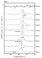
- the light-transmissive substrate 1, the phase shift film 2, the light-shielding film 3, and the hard mask film 4 of Example 1 were analyzed by X-ray photoelectron spectroscopy.
- the result of the state analysis is shown in FIG. 3, the result of the chemical bond state analysis in the depth direction of the N1s narrow spectrum is shown in FIG. 4, and the result of the chemical bond state analysis in the depth direction of the O1s narrow spectrum is shown in FIG.
- the energy distribution of photoelectrons emitted from the hard mask film 4 is measured by irradiating the surface of the mask blank 100 (hard mask film 4) with X-rays.
- the hard mask film 4 is dug for a predetermined time by Ar gas sputtering, and the surface of the hard mask film 4 in the dug region is irradiated with X-rays to measure the energy distribution of photoelectrons emitted from the hard mask film 4.
- the analysis in the film thickness direction is performed in the order of the hard mask film 4, the light-shielding film 3, the phase shift film 2, and the translucent substrate 1.
- each of the narrow spectra of “9.00 min plot” and “14.00 min plot” has the scale of the vertical axis greatly expanded as compared with the narrow spectra of other plots. That is, the vibration waves in the narrow spectra of the “9.00 min plot” and the “14.00 min plot” of the Si2p narrow spectrum in FIG. 3 show noise, not the presence of peaks. Only. This result indicates that the silicon content is below the lower limit of detection at the position in the film thickness direction corresponding to each Si2p narrow spectrum of the light-shielding film 3.
- the analysis result at the position in the film thickness direction of the hard mask film 4 after digging by 1.00 min from the outermost surface of the light-shielding film 3 by Ar gas sputtering shows that the hard mask film 4 except for the surface layer part is removed. It is a measurement result.
- the hard mask film 4 of Example 1 has the maximum peak at the binding energy between 103 and 104 eV.
- This result means that Si—O bonds are present at a certain ratio or more (SiO 2 is the main component).
- SiO 2 is the main component.
- the hard mask film 4 of Example 1 has a substantially flat waveform with a binding energy between 97 eV and 100 eV or less and has no peak. This result means that the presence of Si-Si bond was not detected.
- the hard mask film 4 of Example 1 has the maximum peak at the binding energy between 398 and 399 eV.
- This result means that Si—N bonds are present in a certain ratio or more.
- there is no difference (less than 0.05 eV). In this regard, it was found to be preferable in order to obtain high controllability during the etching process of the hard mask film.
- the hard mask film 4 of Example 1 has the maximum peak at the binding energy between 532 and 533 eV.
- This result means that Si—O bonds are present at a certain ratio or more.
- phase shift mask 200 of Example 1 was manufactured by the following procedure. First, the surface of the hard mask film 4 was subjected to HMDS treatment.
- the contact angle on the surface of the hard mask film 4 was measured using a fully automatic contact angle meter DM-701 (manufactured by Kyowa Interface Science Co., Ltd.) at room temperature of 23° C.
- the average value of the contact angle of water measured at each measurement point was 59.7 degrees (deg).
- a resist film made of a chemically amplified resist for electron beam writing was formed with a film thickness of 70 nm (previously 80 nm) in contact with the surface of the hard mask film 4 by a spin coating method.
- a first pattern which is a phase shift pattern to be formed on the phase shift film 2 is electron-beam-drawn, subjected to a predetermined development process and a cleaning process, and a resist having the first pattern is performed.
- a pattern 5a was formed (see FIG. 2A).
- This first pattern is a pattern (phase shift pattern) including a fine pattern (SRAF pattern having a line width of 35 nm or less (conventional 40 nm or less)) to be formed on the phase shift film 2.
- the resist pattern 5a formed on the hard mask film 4 was good in that no collapse of the resist pattern was observed.
- over-etching was additionally performed for 50% of the just etching time (over-etching time).
- over-etching time 50% of the just etching time.
- a resist film made of a chemically amplified resist for electron beam writing having a film thickness of 150 nm was formed on the light shielding pattern 3a by a spin coating method.
- a second pattern which is a pattern to be formed on the light-shielding film (a pattern including a light-shielding band pattern), is exposed and drawn on the resist film, and further subjected to a predetermined process such as development processing to have a light-shielding pattern.
- a resist pattern 6b was formed (see FIG. 2E).
- a second pattern (light-shielding pattern 3b) was formed in No. 3 (see FIG. 2 (f)). Further, the resist pattern 6b was removed, and a predetermined process such as cleaning was performed to obtain a phase shift mask 200 (see FIG. 2G).
- Comparative Example 1 is the same as Example 1 except for the film forming conditions of the hard mask film 4.
- FIG. 2 points different from the first embodiment will be described.
- the hard mask film 4 of Comparative Example 1 had the maximum peak at the binding energy between 103 and 104 eV. This result means that Si—O bonds are present in a certain ratio or more (SiO 2 is the main component). Further, the hard mask film 4 of Comparative Example 1 has a clear peak at a binding energy between 97 and 100 eV, though not as high as a binding energy between 103 and 104 eV. This result means that the Si—Si bond exists in the hard mask film 4 of Comparative Example 1 at a certain ratio or more.
- phase shift mask Next, using the mask blank 100 of Comparative Example 1, a halftone type phase shift mask 200 was manufactured in the same manner as in Example 1. First, the surface of the hard mask film 4 was subjected to HMDS treatment. The average value of the contact angle of water measured at each measurement point was 53.6 degrees.
- This first pattern is a pattern (phase shift pattern) including a fine pattern (SRAF pattern having a line width of 35 nm or less (conventional 40 nm or less)) to be formed on the phase shift film 2.
- SRAF pattern having a line width of 35 nm or less (conventional 40 nm or less)
- the produced transfer mask became a mask with a pattern defect. It is considered that this is because the surface of the hard mask film 4 has a relatively small hydrophobicity (adhesion to the resist is relatively small). Since there are defects, the manufacturing yield of the transfer mask is correspondingly low.
- SEM scanning electron microscope
- Example 2 [Manufacture of mask blanks]
- the hard mask film 4 was formed of silicon oxide, and a mask blank and a transfer mask were manufactured.
- Example 1 is different from the material of the hard mask film 4 and the film forming method thereof. Is the same as.
- the parts different from those of the first embodiment will be described.
- the phase shift film 2 and the light shielding film 3 were formed in the same procedure as in Example 1. Subsequently, sputtering is performed using a target of silicon (Si) and oxygen (O 2 ) and argon (Ar) gas as sputtering gas, thereby forming a hard mask made of a SiO film having a thickness of 15 nm on the light shielding film 3.
- the film 4 was formed.
- the hard mask film 4 of Comparative Example 2 has a maximum peak of Si—O bond at a binding energy of less than 103 eV and a maximum peak of Si—Si bond at a binding energy of 98 to 99 eV. It was found that it had a peak (the area strength was about the same). This result means that the Si—O bond and the Si—Si bond exist in the same ratio.
- phase shift mask Next, using the mask blank 100 of Comparative Example 2, a halftone type phase shift mask 200 was manufactured in the same manner as in Example 1. First, the surface of the hard mask film 4 was subjected to HMDS treatment. The average value of the contact angle of water measured at each measurement point was 49.7 degrees.
- This first pattern is a pattern (phase shift pattern) including a fine pattern (SRAF pattern having a line width of 35 nm or less (conventional 40 nm or less)) to be formed on the phase shift film 2.
- SRAF pattern having a line width of 35 nm or less (conventional 40 nm or less)
- the manufactured transfer mask became a mask having a pattern defect. It is considered that this is because the surface of the hard mask film 4 has relatively low hydrophobicity (adhesion to the resist is relatively low). Due to the defects, the manufacturing yield of the transfer mask was correspondingly low.
- Translucent substrate 2 Phase shift film 2a Phase shift pattern 3 Light-shielding film (thin film for pattern formation) 3a, 3b Light-shielding pattern 4 Hard mask film 4a Hard mask pattern 5a Resist pattern 6b Resist pattern 11 Substrate 12 Multilayer reflective film 13 Protective film 14 Absorber film (phase shift film) 15 hard mask film 16 back surface conductive film 100 mask blank 200 phase shift mask (transfer mask) 300 Reflective Mask Blank 400 Reflective Mask
Landscapes
- Physics & Mathematics (AREA)
- General Physics & Mathematics (AREA)
- Preparing Plates And Mask In Photomechanical Process (AREA)
- Drying Of Semiconductors (AREA)
- Exposure And Positioning Against Photoresist Photosensitive Materials (AREA)
Abstract
マスクパターンやハードマスクパターンのさらなる微細化及びパターン品質の向上が可能なマスクブランクを提供することを課題とし、当該課題を解決するために、基板(1)上に、パターン形成用薄膜(3)とハードマスク膜(4)がこの順に積層した構造を備えるマスクブランク(100)において、ハードマスク膜(4)を、ケイ素と酸素と窒素を含有する材料で構成するとともに、窒素の含有量を2%以上18%以下、X線光電子分光法で分析して得られるSi2pのナロースペクトルが103eV以上の結合エネルギーで最大ピークを有するように、構成した。
Description
本発明は、マスクブランク、このマスクブランクを用いる転写用マスクの製造方法、及び、このマスクブランクから製造された転写用マスクを用いる半導体デバイスの製造方法に関する。
ハーフトーン型位相シフトマスクのマスクブランクとして、透光性基板上に金属シリサイド系材料からなるハーフトーン位相シフト膜、クロム系材料からなる遮光膜、無機系材料からなるエッチングマスク膜(ハードマスク膜)が積層された構造を有するマスクブランクが知られている(例えば、特許文献1参照)。このマスクブランクを用いて位相シフトマスクを製造する場合、先ず、マスクブランクの表面に形成したレジストパターンをマスクとしてフッ素系ガスによるドライエッチングでエッチングマスク膜をパターニングする。次に、エッチングマスク膜をマスクとして塩素と酸素の混合ガスによるドライエッチングで遮光膜をパターニングする。さらに、遮光膜のパターンをマスクとしてフッ素系ガスによるドライエッチングで位相シフト膜をパターニングする。
特許文献1に記載されているようなマスクブランクにおいて、クロム系化合物からなる遮光膜は、位相シフト膜を透過した露光光を所定以下の光量に低下させる遮光性能を備えることが求められる。このマスクブランクから位相シフトマスクを作製する際、遮光膜に遮光帯を含むパターンが形成される。そして、位相シフト膜と遮光膜の積層構造で所定の光学濃度を満たすことが求められる。同時に、この遮光膜には、位相シフト膜をフッ素系ガスのドライエッチングによってパターニングして位相シフトパターンを形成するときに、エッチングマスクとして機能することが求められる。位相シフトマスクの完成段階では、遮光膜には遮光パターン等の比較的疎なパターンが形成されるのが一般的である。しかし、マスクブランクから位相シフトマスクを製造する途上において、遮光膜は位相シフト膜に微細な転写パターンである位相シフトパターンを形成するときにエッチングマスクとして機能する必要がある。このため、遮光膜においても微細パターンを高い寸法精度で形成できることが望まれる。
クロム系材料からなる遮光膜のドライエッチングでは、塩素系ガスと酸素ガスとの混合ガス(酸素含有塩素系ガス)がエッチングガスとして用いられる。一般に、この酸素含有塩素系ガスをエッチングガスとして用いるドライエッチングは、異方性エッチングの傾向が小さく、等方性エッチングの傾向が大きい。
一般に、ドライエッチングによってパターン形成用薄膜にパターンを形成する場合、エッチングが膜の厚さ方向のみならず、薄膜に形成されるパターンの側壁方向へのエッチング、いわゆるサイドエッチングが進む。このサイドエッチングの進行を抑制するために、ドライエッチングの際、基板の、薄膜が形成されている主表面の反対側からバイアス電圧を掛け、エッチングガスが膜の厚さ方向に、より多く接触するように制御することがこれまでも行われている。フッ素系ガスのように、イオン性のプラズマになる傾向が大きいエッチングガスを用いる、イオン主体のドライエッチングの場合には、バイアス電圧を掛けることよるエッチング方向の制御性が高く、エッチングの異方性が高められるため、エッチングされる薄膜のサイドエッチング量を微小にできる。
一方、酸素含有塩素系ガスによるドライエッチングの場合、酸素ガスはラジカル性のプラズマになる傾向が高いため、バイアス電圧を掛けることによるエッチング方向の制御の効果が小さく、エッチングの異方性を高めることが難しい。このため、酸素含有塩素系ガスを用いるドライエッチングによって、クロム系材料からなる遮光膜にパターンを形成する場合、サイドエッチング量が大きくなりやすい。
有機系材料からなるレジストパターンをエッチングマスクとして、酸素含有塩素系ガスを用いたドライエッチングでクロム系材料の遮光膜をパターニングする場合、レジストパターンは、上方からエッチングされて減退していく。このとき、レジストパターンの側壁方向もエッチングされて減退する。このため、レジスト膜に形成するパターンの幅は、予めサイドエッチングによる減退量を見込んで設計されている。さらに、レジスト膜に形成するパターンの幅は、クロム系材料の遮光膜のサイドエッチング量も見込んで設計されている。
近年、クロム系材料の遮光膜の上に、酸素含有塩素系ガスのドライエッチングに対し、クロム系材料との間で十分なエッチング選択性を有する材料からなる、エッチングマスク膜(ハードマスク膜)を設けたマスクブランクが用いられ始めている。このマスクブランクでは、レジストパターンをマスクとするドライエッチングによってハードマスク膜にパターンを形成する。そして、パターンが形成されたハードマスク膜をマスクとし、酸素含有塩素系ガスのドライエッチングを遮光膜に対して行い、遮光膜にパターンを形成する。このハードマスク膜は、フッ素系ガスのドライエッチングでパターニング可能な材料で形成されるのが一般的である。フッ素系ガスのドライエッチングは、イオン主体のエッチングであるため、異方性エッチングの傾向が大きい。このため、位相シフトパターンが形成されたハードマスク膜におけるパターン側壁のサイドエッチング量は小さい。また、フッ素系ガスのドライエッチングの場合、ハードマスク膜にパターンを形成するためのレジストパターンにおいても、サイドエッチング量が小さくなる傾向がある。このため、クロム系材料の遮光膜についても、酸素含有塩素系ガスのドライエッチングにおけるサイドエッチング量が小さいことが望まれる。
このクロム系材料の遮光膜におけるサイドエッチング量を小さくする手段として、酸素含有塩素系ガスのドライエッチングにおいて、酸素含有塩素系ガス中の塩素系ガスの混合比率を大幅に高めることが検討されている。塩素系ガスは、イオン性のプラズマになる傾向が大きいからである。塩素系ガスの比率を高めた酸素含有塩素系ガスを用いたドライエッチングでは、クロム系材料の遮光膜のエッチングレートが低下することは避けられない。このクロム系材料の遮光膜のエッチングレートの低下を補うために、ドライエッチング時に掛けられるバイアス電圧を大幅に高くする(以下、塩素系ガスの比率を高めた酸素含有塩素系ガスを用い、かつ高いバイアス電圧を掛けた状態下で行われるドライエッチングのことを、「酸素含有塩素系ガスの高バイアスエッチング」という。)ことも検討されている。
この酸素含有塩素系ガスの高バイアスエッチングによるクロム系材料の遮光膜に対するエッチングレートは、従来のエッチング条件でドライエッチングを行う場合と遜色ないレベルである。エッチング時に生じる遮光膜のサイドエッチング量も従来よりも小さくすることができる。
さらに、クロム系材料の遮光膜における結合や組成を検討し調整等することによって、パターンが形成されたハードマスク膜をマスクとし、酸素含有塩素系ガスをエッチングガスに用い、かつ高バイアスエッチング条件で遮光膜をパターニングした場合、形成された遮光膜のパターンのサイドエッチング量を大幅に低減することができ、この結果、位相シフト膜に精度よく微細なパターンを形成することができる(特許文献2)。
しかし、位相シフト膜に形成すべきパターンのさらなる微細化が求められており、そのためには上述した遮光膜のパターンのサイドエッチング量を大幅に低減する等の技術のみでは十分ではない。また、遮光膜等のパターン形成用薄膜に形成すべきパターンやハードマスク膜に形成すべきパターンのさらなる微細化およびパターン品質の向上が求められている。これらのことは、パターン形成用薄膜である遮光膜等を有するバイナリマスクや、パターン形成用薄膜である吸収体膜等を有する反射型マスクにおいても同様である。
上述した問題の解決のため、本発明は、基板上に、遮光膜等のパターン形成用薄膜とハードマスク膜がこの順に積層した構造を備えるマスクブランクに関し、遮光膜等のパターン形成用薄膜に形成すべきパターンや、ハードマスク膜に形成すべきパターンのさらなる微細化およびパターン品質の向上が可能なマスクブランクを提供しようとするものである。
特に、本発明は、高バイアスエッチング条件に適した優れた性能を有するハードマスク膜を有し、パターン形成用薄膜に形成すべきパターンのさらなる微細化およびパターン品質の向上が可能なマスクブランクを提供しようとするものである。
また、本発明は、このマスクブランクを用いることにより、パターン形成用薄膜に精度よく微細なパターンを形成することが可能な転写用マスクの製造方法を提供しようとするものである。
本発明はさらに、その転写用マスクを用いる半導体デバイスの製造方法を提供しようとするものである。
特に、本発明は、高バイアスエッチング条件に適した優れた性能を有するハードマスク膜を有し、パターン形成用薄膜に形成すべきパターンのさらなる微細化およびパターン品質の向上が可能なマスクブランクを提供しようとするものである。
また、本発明は、このマスクブランクを用いることにより、パターン形成用薄膜に精度よく微細なパターンを形成することが可能な転写用マスクの製造方法を提供しようとするものである。
本発明はさらに、その転写用マスクを用いる半導体デバイスの製造方法を提供しようとするものである。
本発明は上記の課題を解決する手段として、以下の構成を有する。
(構成1)
基板上に、パターン形成用薄膜とハードマスク膜がこの順に積層した構造を備えるマスクブランクであって、
前記ハードマスク膜は、ケイ素と酸素と窒素を含有する材料からなり、
前記ハードマスク膜は、窒素の含有量が2原子%以上18原子%以下であり、
前記ハードマスク膜は、X線光電子分光法で分析して得られるSi2pのナロースペクトルが103eV以上の結合エネルギーで最大ピークを有する
ことを特徴とするマスクブランク。
基板上に、パターン形成用薄膜とハードマスク膜がこの順に積層した構造を備えるマスクブランクであって、
前記ハードマスク膜は、ケイ素と酸素と窒素を含有する材料からなり、
前記ハードマスク膜は、窒素の含有量が2原子%以上18原子%以下であり、
前記ハードマスク膜は、X線光電子分光法で分析して得られるSi2pのナロースペクトルが103eV以上の結合エネルギーで最大ピークを有する
ことを特徴とするマスクブランク。
(構成2)
前記ハードマスク膜は、X線光電子分光法で分析して得られるSi2pのナロースペクトルが97eV以上100eV以下の結合エネルギーの範囲でピークを有さないことを特徴とする構成1に記載のマスクブランク。
(構成3)
前記ハードマスク膜の表面をX線光電子分光法で分析して得られるSi2pのナロースペクトルで最大ピークとなる結合エネルギーと、前記ハードマスク膜の内部をX線光電子分光法で分析して得られるSi2pのナロースペクトルで最大ピークとなる結合エネルギーとの差が0.2eV以下であることを特徴とする構成1または2に記載のマスクブランク。
前記ハードマスク膜は、X線光電子分光法で分析して得られるSi2pのナロースペクトルが97eV以上100eV以下の結合エネルギーの範囲でピークを有さないことを特徴とする構成1に記載のマスクブランク。
(構成3)
前記ハードマスク膜の表面をX線光電子分光法で分析して得られるSi2pのナロースペクトルで最大ピークとなる結合エネルギーと、前記ハードマスク膜の内部をX線光電子分光法で分析して得られるSi2pのナロースペクトルで最大ピークとなる結合エネルギーとの差が0.2eV以下であることを特徴とする構成1または2に記載のマスクブランク。
(構成4)
前記ハードマスク膜の表面をX線光電子分光法で分析して得られるN1sのナロースペクトルで最大ピークとなる結合エネルギーと、前記ハードマスク膜の内部をX線光電子分光法で分析して得られるN1sのナロースペクトルで最大ピークとなる結合エネルギーとの差が0.2eV以下であることを特徴とする構成1から3のいずれかに記載のマスクブランク。
(構成5)
前記ハードマスク膜の表面をX線光電子分光法で分析して得られるO1sのナロースペクトルで最大ピークとなる結合エネルギーと、前記ハードマスク膜の内部をX線光電子分光法で分析して得られるO1sのナロースペクトルで最大ピークとなる結合エネルギーとの差が0.2eV以下であることを特徴とする構成1から4のいずれかに記載のマスクブランク。
前記ハードマスク膜の表面をX線光電子分光法で分析して得られるN1sのナロースペクトルで最大ピークとなる結合エネルギーと、前記ハードマスク膜の内部をX線光電子分光法で分析して得られるN1sのナロースペクトルで最大ピークとなる結合エネルギーとの差が0.2eV以下であることを特徴とする構成1から3のいずれかに記載のマスクブランク。
(構成5)
前記ハードマスク膜の表面をX線光電子分光法で分析して得られるO1sのナロースペクトルで最大ピークとなる結合エネルギーと、前記ハードマスク膜の内部をX線光電子分光法で分析して得られるO1sのナロースペクトルで最大ピークとなる結合エネルギーとの差が0.2eV以下であることを特徴とする構成1から4のいずれかに記載のマスクブランク。
(構成6)
前記ハードマスク膜は、酸素の含有量が50原子%以上であることを特徴とする構成1から5のいずれかに記載のマスクブランク。
(構成7)
前記ハードマスク膜は、ケイ素と酸素と窒素とからなる材料、または半金属元素および非金属元素から選ばれる1以上の元素とケイ素と酸素と窒素とからなる材料で形成されていることを特徴とする構成1から6のいずれかに記載のマスクブランク。
前記ハードマスク膜は、酸素の含有量が50原子%以上であることを特徴とする構成1から5のいずれかに記載のマスクブランク。
(構成7)
前記ハードマスク膜は、ケイ素と酸素と窒素とからなる材料、または半金属元素および非金属元素から選ばれる1以上の元素とケイ素と酸素と窒素とからなる材料で形成されていることを特徴とする構成1から6のいずれかに記載のマスクブランク。
(構成8)
前記パターン形成用薄膜は、クロム、タンタルおよびニッケルから選ばれる1以上の元素を含有する材料からなることを特徴とする構成1から7のいずれかに記載のマスクブランク。
(構成9)
前記パターン形成用薄膜は、遮光膜であることを特徴とする構成1から8のいずれかに記載のマスクブランク。
前記パターン形成用薄膜は、クロム、タンタルおよびニッケルから選ばれる1以上の元素を含有する材料からなることを特徴とする構成1から7のいずれかに記載のマスクブランク。
(構成9)
前記パターン形成用薄膜は、遮光膜であることを特徴とする構成1から8のいずれかに記載のマスクブランク。
(構成10)
前記基板と前記遮光膜の間に位相シフト膜を備えることを特徴とする構成9記載のマスクブランク。
(構成11)
前記基板と前記パターン形成用薄膜との間に多層反射膜を備え、前記パターン形成用薄膜は、吸収体膜または位相シフト膜であることを特徴とする構成1から7のいずれかに記載のマスクブランク。
前記基板と前記遮光膜の間に位相シフト膜を備えることを特徴とする構成9記載のマスクブランク。
(構成11)
前記基板と前記パターン形成用薄膜との間に多層反射膜を備え、前記パターン形成用薄膜は、吸収体膜または位相シフト膜であることを特徴とする構成1から7のいずれかに記載のマスクブランク。
(構成12)
構成1から11のいずれかに記載のマスクブランクを用いる転写用マスクの製造方法であって、
前記ハードマスク膜上に形成された、転写パターンを有するレジスト膜をマスクとし、フッ素系ガスを用いたドライエッチングにより、前記ハードマスク膜に転写パターンを形成する工程と、
前記転写パターンが形成されたハードマスク膜をマスクとし、塩素を含有するガスを用いたドライエッチングにより、前記パターン形成用薄膜に転写パターンを形成する工程とを有することを特徴とする転写用マスクの製造方法。
(構成13)
前記塩素を含有するガスを用いたドライエッチングは、塩素系ガスの比率を高めた酸素含有塩素系ガスを用い、かつ高いバイアス電圧を掛けた状態下で行われるドライエッチングであることを特徴とする構成12に記載の転写用マスクの製造方法。
(構成14)
前記塩素を含有するガスを用いたドライエッチングは、酸素含有しない塩素系ガスを用い、かつ高いバイアス電圧を掛けた状態下で行われるドライエッチングであることを特徴とする構成12に記載の転写用マスクの製造方法。
(構成15)
構成12から14のいずれかに記載の転写用マスクの製造方法によって製造した転写用マスクを用い、半導体デバイスを形成する基板上のレジスト膜に転写パターンを露光転写する工程を備えることを特徴とする半導体デバイスの製造方法。
構成1から11のいずれかに記載のマスクブランクを用いる転写用マスクの製造方法であって、
前記ハードマスク膜上に形成された、転写パターンを有するレジスト膜をマスクとし、フッ素系ガスを用いたドライエッチングにより、前記ハードマスク膜に転写パターンを形成する工程と、
前記転写パターンが形成されたハードマスク膜をマスクとし、塩素を含有するガスを用いたドライエッチングにより、前記パターン形成用薄膜に転写パターンを形成する工程とを有することを特徴とする転写用マスクの製造方法。
(構成13)
前記塩素を含有するガスを用いたドライエッチングは、塩素系ガスの比率を高めた酸素含有塩素系ガスを用い、かつ高いバイアス電圧を掛けた状態下で行われるドライエッチングであることを特徴とする構成12に記載の転写用マスクの製造方法。
(構成14)
前記塩素を含有するガスを用いたドライエッチングは、酸素含有しない塩素系ガスを用い、かつ高いバイアス電圧を掛けた状態下で行われるドライエッチングであることを特徴とする構成12に記載の転写用マスクの製造方法。
(構成15)
構成12から14のいずれかに記載の転写用マスクの製造方法によって製造した転写用マスクを用い、半導体デバイスを形成する基板上のレジスト膜に転写パターンを露光転写する工程を備えることを特徴とする半導体デバイスの製造方法。
以上の構成を有する本発明によれば、基板上に、遮光膜等のパターン形成用薄膜とハードマスク膜がこの順に積層した構造を備えるマスクブランクであって、遮光膜等のパターン形成用薄膜に形成すべきパターンや、ハードマスク膜に形成すべきパターンのさらなる微細化およびパターン品質の向上が可能なマスクブランクを提供できる。
特に、本発明によれば、高バイアスエッチング条件に適した優れた性能を有するハードマスク膜を有し、パターン形成用薄膜に形成すべきパターンのさらなる微細化およびパターン品質の向上が可能なマスクブランクを提供できる。
本発明によれば、また、このマスクブランクを用いることにより、パターン形成用薄膜に精度よく微細なパターンを形成することが可能な転写用マスクの製造方法を提供できる。
本発明によれば、さらに、その転写用マスクを用いる半導体デバイスの製造方法を提供できる。
特に、本発明によれば、高バイアスエッチング条件に適した優れた性能を有するハードマスク膜を有し、パターン形成用薄膜に形成すべきパターンのさらなる微細化およびパターン品質の向上が可能なマスクブランクを提供できる。
本発明によれば、また、このマスクブランクを用いることにより、パターン形成用薄膜に精度よく微細なパターンを形成することが可能な転写用マスクの製造方法を提供できる。
本発明によれば、さらに、その転写用マスクを用いる半導体デバイスの製造方法を提供できる。
以下、本発明の実施形態について説明するが、まず本発明に至った経緯について説明する。
本発明者らは、ハードマスク膜に形成されるパターンのさらなる微細化およびパターン品質の向上について研究した。その結果、以下のことが判明した。
第1に、ケイ素と酸素を含有する材料からなるハードマスク膜は、膜中にSi-N結合を有する(窒素を含有する)と、膜中にSi-N結合を有しない(窒素を含有しない)場合(SiO2)に比べ、フッ素系ガスに対するエッチングレートが大きく、ハードマスク膜が速くきれいにエッチング加工できることがわかった。ハードマスク膜のエッチング時間が短くてすむ分、レジストを薄くできる。レジストを薄くできる分だけ、より微細なレジストパターンの倒れを防止でき、より微細なレジストパターンの形成を実現できる。
本発明者らは、ハードマスク膜に形成されるパターンのさらなる微細化およびパターン品質の向上について研究した。その結果、以下のことが判明した。
第1に、ケイ素と酸素を含有する材料からなるハードマスク膜は、膜中にSi-N結合を有する(窒素を含有する)と、膜中にSi-N結合を有しない(窒素を含有しない)場合(SiO2)に比べ、フッ素系ガスに対するエッチングレートが大きく、ハードマスク膜が速くきれいにエッチング加工できることがわかった。ハードマスク膜のエッチング時間が短くてすむ分、レジストを薄くできる。レジストを薄くできる分だけ、より微細なレジストパターンの倒れを防止でき、より微細なレジストパターンの形成を実現できる。
なお、ある膜のエッチングレートが増大すると、その膜をパターニングするときのエッチングタイムが短くなる。その膜をパターニングするときのエッチングタイムが短くなると、その膜の側壁がエッチングガスに晒される時間が短くなり、サイドエッチング量が減少することにつながる。これに加え、本発明では、ハードマスク膜が速くエッチング加工できる。これにより、側壁ラフネスが小さく、きれい(平滑)な側壁を有するパターンを形成できる。パターン側壁の垂直性も良好である。
特に、ある膜のエッチングレートが大幅に速くなる場合、膜厚方向のエッチングタイムが大きく短縮され、ある膜の側壁がエッチングガスに晒される時間が大幅に短くなる。これにより、ハードマスク膜のパターンの側壁ラフネスがより小さく、よりきれい(平滑)な側壁を有するパターンを形成できる。
特に、ある膜のエッチングレートが大幅に速くなる場合、膜厚方向のエッチングタイムが大きく短縮され、ある膜の側壁がエッチングガスに晒される時間が大幅に短くなる。これにより、ハードマスク膜のパターンの側壁ラフネスがより小さく、よりきれい(平滑)な側壁を有するパターンを形成できる。
第2に、ケイ素と酸素を含有する材料からなるハードマスク膜は、膜中にSi-N結合を有する(窒素を含有する)と、膜中にSi-N結合を有しない(窒素を含有しない)場合(SiO2)に比べ、HMDS(Hexamethyldisilazane)処理後の接触角が大きく、レジストの密着性が良いことがわかった。このため、より微細なレジストパターンの倒れを防止でき、より微細なレジストパターンの形成を実現できる。なお、レジストパターンがより微細なものになると、密着性がその分低下してしまうが、本発明では、その影響を抑制することができる。
本発明では、より微細なレジストパターンの倒れを防止でき、より微細なレジストパターンの形成を実現できる。この結果、ハードマスク膜に形成されるパターンのさらなる微細化を実現できる。
本発明では、より微細なレジストパターンの倒れを防止でき、より微細なレジストパターンの形成を実現できる。この結果、ハードマスク膜に形成されるパターンのさらなる微細化を実現できる。
上記第1と第2の二つの効果を得るためには、少なくとも、X線光電子分光法(XPS:X-ray Photoelectron Spectroscopy)で分析して得られるN1sのナロースペクトルの最大ピークが検出されること(最大ピークが検出限界以下ではないこと)、すなわち実質的に窒素が含有されていることが必要である。
上記第1と第2の二つの効果を得るためには、ケイ素と酸素と窒素を含有する材料からなるハードマスク膜の窒素の含有量は、2原子%以上が好ましく、3原子%以上がより好ましく、4原子%以上がさらに好ましく、5原子%以上がより一層好ましい。窒素の含有量が少なすぎると、上記二つの効果が得られにくい。
なお、本発明に係るケイ素と酸素と窒素を含有する材料からなるハードマスク膜は、X線光電子分光法で分析して得られるN1sのナロースペクトルが398eV以上の結合エネルギーで最大ピークを有する。
上記第1と第2の二つの効果を得るためには、ケイ素と酸素と窒素を含有する材料からなるハードマスク膜の窒素の含有量は、2原子%以上が好ましく、3原子%以上がより好ましく、4原子%以上がさらに好ましく、5原子%以上がより一層好ましい。窒素の含有量が少なすぎると、上記二つの効果が得られにくい。
なお、本発明に係るケイ素と酸素と窒素を含有する材料からなるハードマスク膜は、X線光電子分光法で分析して得られるN1sのナロースペクトルが398eV以上の結合エネルギーで最大ピークを有する。
次に、本発明者らは、ハードマスクとしての機能低下、および、これによるパターン転写性能の低下について研究した。
その結果、第3に、ケイ素と酸素と窒素を含有する材料からなるハードマスク膜は、窒素が多くなるに従い、ハードマスクとしての機能が下がる(塩素系ガスに対するエッチング耐性が若干低下する)傾向にあることがわかった。そして、窒素の含有量が18原子%以下であれば、ハードマスクとしての機能低下が抑制でき、パターン転写性能の低下は避けられることがわかった。それに加え、ケイ素と酸素と窒素を含有する材料からなるハードマスク膜は、X線光電子分光法で分析して得られるSi2pのナロースペクトルが103eV以上の結合エネルギーで最大ピークを有することも必要であることもわかった。ハードマスク膜中のSiO2結合とSi-O結合の存在比率が高いことによって、ハードマスクとしての機能を確保できる。ハードマスク膜がこれらの特徴を備えることによって、上記第1と第2の二つの効果を維持しつつ、上記第3の影響を抑えることができる。
その結果、第3に、ケイ素と酸素と窒素を含有する材料からなるハードマスク膜は、窒素が多くなるに従い、ハードマスクとしての機能が下がる(塩素系ガスに対するエッチング耐性が若干低下する)傾向にあることがわかった。そして、窒素の含有量が18原子%以下であれば、ハードマスクとしての機能低下が抑制でき、パターン転写性能の低下は避けられることがわかった。それに加え、ケイ素と酸素と窒素を含有する材料からなるハードマスク膜は、X線光電子分光法で分析して得られるSi2pのナロースペクトルが103eV以上の結合エネルギーで最大ピークを有することも必要であることもわかった。ハードマスク膜中のSiO2結合とSi-O結合の存在比率が高いことによって、ハードマスクとしての機能を確保できる。ハードマスク膜がこれらの特徴を備えることによって、上記第1と第2の二つの効果を維持しつつ、上記第3の影響を抑えることができる。
上記第3の傾向は、酸素含有塩素系ガスの高バイアスエッチング条件で大きくなり、ハードマスクとしての機能が下がる(塩素系ガスに対するエッチング耐性が低下する)傾向にあることがわかった。すなわち、ハードマスク膜のパターンのエッジ部分がエッチングされやすくなることで、ラインエッジラフネス(LER:Line Edge Roughness)が悪化し、形成された遮光パターンの精度が悪化する傾向にあることがわかった。
ケイ素と酸素と窒素を含有する材料からなるハードマスク膜の場合、窒素の含有量は、15原子%以下が好ましく、12原子%以下がより好ましく、10原子%以下がさらに好ましく、8原子%以下がより一層好ましい。
なお、通常、パターン形成用薄膜をドライエッチングする際には、化学反応によるエッチングと物理的作用によるエッチングの両方が行われる。化学反応によるエッチングは、プラズマ状態のエッチングガスが薄膜の表面に接触し、薄膜中のケイ素または金属元素と結合して低沸点の化合物(例えばSiF4、CrO2Cl2等)を生成して昇華するプロセスで行われる。化学反応によるエッチングでは、他の元素(例えば、O、N等)と結合状態にあるケイ素または金属元素に対し、その結合を断ち切らせて低沸点の化合物を生成する。これに対し、物理的なエッチングは、バイアス電圧によって加速されたエッチングガス中のイオン性のプラズマが薄膜の表面に衝突すること(この現象を「イオン衝撃」ともいう。)で、薄膜表面のケイ素または金属元素を含む各元素を物理的にはじき飛ばし(このとき元素間の結合が断ち切られる。)、そのケイ素または金属元素と低沸点の化合物を生成して昇華するプロセスで行われる。
高バイアスエッチングは、通常条件のドライエッチングに比べて物理的作用によるドライエッチングを高めたものである。物理的作用によるエッチングは、膜厚方向へのエッチングに対して大きく寄与するが、パターンの側壁方向へのエッチングにはあまり寄与しない。
これに対し、化学反応によるエッチングは、膜厚方向へのエッチング及びパターンの側壁方向へのエッチング(サイドエッチング)のいずれにも寄与するものである。
これに対し、化学反応によるエッチングは、膜厚方向へのエッチング及びパターンの側壁方向へのエッチング(サイドエッチング)のいずれにも寄与するものである。
次に、本発明者らは、酸素含有塩素系ガスの高バイアスエッチング条件に適したハードマスク膜について研究した。
その結果、第4に、ケイ素と酸素と窒素を含有する材料からなるハードマスク膜は、膜中にSi-Si結合を有し、X線光電子分光法で分析して得られるSi2pのナロースペクトルでSi-Si結合に対応するピークが確認できる場合、Si-Si結合が多くなるに従い、ハードマスクとしての機能が大きく下がる(塩素系ガスに対するエッチング耐性が大きく低下する)傾向にあることがわかった。このため、パターン転写性能の低下は避けられないことがわかった。この傾向は、酸素含有塩素系ガスの高バイアスエッチング条件でさらに大きくなるとがわかった。
その結果、第4に、ケイ素と酸素と窒素を含有する材料からなるハードマスク膜は、膜中にSi-Si結合を有し、X線光電子分光法で分析して得られるSi2pのナロースペクトルでSi-Si結合に対応するピークが確認できる場合、Si-Si結合が多くなるに従い、ハードマスクとしての機能が大きく下がる(塩素系ガスに対するエッチング耐性が大きく低下する)傾向にあることがわかった。このため、パターン転写性能の低下は避けられないことがわかった。この傾向は、酸素含有塩素系ガスの高バイアスエッチング条件でさらに大きくなるとがわかった。
本発明では、ケイ素と酸素と窒素を含有する材料からなるハードマスク膜は、X線光電子分光法で分析して得られるSi2pのナロースペクトルでSi-Si結合に対応するピーク(97eV以上100eV以下の結合エネルギーの範囲でのピーク)が確認できない(検出限界値以下である)ことが好ましい。このようなハードマスク膜は、Si-Si結合を有しない、あるいはSi-Si結合の存在比率がかなり低いといえる。これにより、ハードマスクに関する上記第4の好ましくない傾向の影響が避けられる。その結果、ハードマスクに起因するパターン転写性能の低下が避けられる。
次に、本発明者らは、ハードマスク膜に含まれる結合の種類、結合エネルギー(ナロースペクトル)について研究した。具体的には、ハードマスク膜の表面をX線光電子分光法で分析して得られるSi2pのナロースペクトルで最大ピークとなる結合エネルギーと、前記ハードマスク膜の内部をX線光電子分光法で分析して得られるSi2pのナロースペクトルで最大ピークとなる結合エネルギーとの差(以下、これをSi2pのナロースペクトルの結合エネルギー差という。)に着目した。
その結果、ケイ素と酸素と窒素を含有する材料からなるハードマスク膜は、Si2pのナロースペクトルの結合エネルギー差が相対的に小さく、膜の厚さ方向(深さ方向)で結合エネルギーがより均一(好ましくは実質同じ)であることが、ハードマスク膜のエッチング加工時に高い制御性を得るためには、好ましいことがわかった。具体的には、Si2pのナロースペクトルの結合エネルギー差が0.2eV以下であることが好ましく、0.1eV以下であることがより好ましいことがわかった。
その結果、ケイ素と酸素と窒素を含有する材料からなるハードマスク膜は、Si2pのナロースペクトルの結合エネルギー差が相対的に小さく、膜の厚さ方向(深さ方向)で結合エネルギーがより均一(好ましくは実質同じ)であることが、ハードマスク膜のエッチング加工時に高い制御性を得るためには、好ましいことがわかった。具体的には、Si2pのナロースペクトルの結合エネルギー差が0.2eV以下であることが好ましく、0.1eV以下であることがより好ましいことがわかった。
次に、ハードマスク膜の表面をX線光電子分光法で分析して得られるN1sのナロースペクトルで最大ピークとなる結合エネルギーと、前記ハードマスク膜の内部をX線光電子分光法で分析して得られるN1sのナロースペクトルで最大ピークとなる結合エネルギーとの差(以下、これをN1sのナロースペクトルの結合エネルギー差という。)についても着目した。
その結果、ケイ素と酸素と窒素を含有する材料からなるハードマスク膜は、N1sのナロースペクトルの結合エネルギー差が相対的に小さく、膜の厚さ方向(深さ方向)で結合エネルギーがより均一(好ましくは実質同じ)であることが、ハードマスク膜のエッチング加工時に高い制御性を得るためには、好ましいことがわかった。具体的には、N1sのナロースペクトルの結合エネルギー差が0.2eV以下であることが好ましく、0.1eV以下であることがより好ましいことがわかった。
その結果、ケイ素と酸素と窒素を含有する材料からなるハードマスク膜は、N1sのナロースペクトルの結合エネルギー差が相対的に小さく、膜の厚さ方向(深さ方向)で結合エネルギーがより均一(好ましくは実質同じ)であることが、ハードマスク膜のエッチング加工時に高い制御性を得るためには、好ましいことがわかった。具体的には、N1sのナロースペクトルの結合エネルギー差が0.2eV以下であることが好ましく、0.1eV以下であることがより好ましいことがわかった。
さらに、ハードマスク膜の表面をX線光電子分光法で分析して得られるO1sのナロースペクトルで最大ピークとなる結合エネルギーと、前記ハードマスク膜の内部をX線光電子分光法で分析して得られるO1sのナロースペクトルで最大ピークとなる結合エネルギーとの差(以下、これをO1sのナロースペクトルの結合エネルギー差という。)についても着目した。
その結果、ケイ素と酸素と窒素を含有する材料からなるハードマスク膜は、O1sのナロースペクトルの結合エネルギー差が相対的に小さく、膜の厚さ方向(深さ方向)で結合エネルギーがより均一(好ましくは実質同じ)であることが、ハードマスク膜のエッチング加工時に高い制御性を得るためには、好ましいことがわかった。具体的には、O1sのナロースペクトルの結合エネルギー差が0.2eV以下であることが好ましく、0.1eV以下であることがより好ましいことがわかった。
その結果、ケイ素と酸素と窒素を含有する材料からなるハードマスク膜は、O1sのナロースペクトルの結合エネルギー差が相対的に小さく、膜の厚さ方向(深さ方向)で結合エネルギーがより均一(好ましくは実質同じ)であることが、ハードマスク膜のエッチング加工時に高い制御性を得るためには、好ましいことがわかった。具体的には、O1sのナロースペクトルの結合エネルギー差が0.2eV以下であることが好ましく、0.1eV以下であることがより好ましいことがわかった。
一方、上記構成のハードマスク膜をマスクとし、酸素を含有しない塩素系ガスをエッチングガスに用いた高バイアスエッチング条件でのドライエッチングで遮光膜をパターニングする場合でも、酸素含有塩素系ガスの高バイアスエッチング条件の場合と同様の作用・効果を奏することも判明した。
以下、図面に基づいて、上述した本発明の詳細な構成を説明する。なお、各図において同様の構成要素には同一の符号を付して説明を行う。
<第1の実施形態>
[マスクブランクとその製造]
〈マスクブランク〉
図1に、本発明に係るマスクブランクの第1の実施形態の概略構成を示す。図1に示すマスクブランク100は、透光性基板1における一方の主表面上に、位相シフト膜2、遮光膜3(パターン形成用薄膜)、及び、ハードマスク膜4がこの順に積層された構成である。また、マスクブランク100は、ハードマスク膜4上に、必要に応じてレジスト膜を積層させた構成であってもよい。以下、マスクブランク100の主要構成部の詳細を説明する。
[マスクブランクとその製造]
〈マスクブランク〉
図1に、本発明に係るマスクブランクの第1の実施形態の概略構成を示す。図1に示すマスクブランク100は、透光性基板1における一方の主表面上に、位相シフト膜2、遮光膜3(パターン形成用薄膜)、及び、ハードマスク膜4がこの順に積層された構成である。また、マスクブランク100は、ハードマスク膜4上に、必要に応じてレジスト膜を積層させた構成であってもよい。以下、マスクブランク100の主要構成部の詳細を説明する。
[透光性基板]
透光性基板1は、リソグラフィーにおける露光工程で用いられる露光光に対して透過性が良好な材料からなる。このような材料としては、合成石英ガラス、アルミノシリケートガラス、ソーダライムガラス、低熱膨張ガラス(SiO2-TiO2ガラス等)、その他各種のガラス基板を用いることができる。特に、合成石英ガラスを用いた基板は、ArFエキシマレーザー光(波長:約193nm)に対する透過性が高いので、マスクブランク100の透光性基板1として好適に用いることができる。
透光性基板1は、リソグラフィーにおける露光工程で用いられる露光光に対して透過性が良好な材料からなる。このような材料としては、合成石英ガラス、アルミノシリケートガラス、ソーダライムガラス、低熱膨張ガラス(SiO2-TiO2ガラス等)、その他各種のガラス基板を用いることができる。特に、合成石英ガラスを用いた基板は、ArFエキシマレーザー光(波長:約193nm)に対する透過性が高いので、マスクブランク100の透光性基板1として好適に用いることができる。
なお、ここで言うリソグラフィーにおける露光工程とは、このマスクブランク100を用いて作製された位相シフトマスクを用いて行なわれるリソグラフィーにおける露光工程であり、以下において露光光とはこの露光工程で用いられる露光光であることとする。この露光光としては、ArFエキシマレーザー光(波長:193nm)、KrFエキシマレーザー光(波長:248nm)、i線光(波長:365nm)のいずれも適用可能であるが、露光工程における位相シフトパターンの微細化の観点からは、ArFエキシマレーザー光を露光光に適用することが望ましい。このため、以下においてはArFエキシマレーザー光を露光光に適用した場合についての実施形態を説明する。
[位相シフト膜]
位相シフト膜2は、露光転写工程で用いられる露光光に対して所定の透過率を有し、かつ位相シフト膜2を透過した露光光が、位相シフト膜2の厚さと同じ距離だけ大気中を通過した露光光に対して、所定の位相差を持つような光学特性を有する。
位相シフト膜2は、露光転写工程で用いられる露光光に対して所定の透過率を有し、かつ位相シフト膜2を透過した露光光が、位相シフト膜2の厚さと同じ距離だけ大気中を通過した露光光に対して、所定の位相差を持つような光学特性を有する。
このような位相シフト膜2は、ここではケイ素(Si)を含有する材料で形成されていることとする。また位相シフト膜2は、ケイ素の他に、窒素(N)を含有する材料で形成されていることが好ましい。このような位相シフト膜2は、フッ素系ガスを用いたドライエッチングによってパターニングが可能であり、後述の遮光膜3を構成するCrOCN膜等に対して、十分なエッチング選択性を有する材料を用いる。
また位相シフト膜2は、フッ素系ガスを用いたドライエッチングによってパターニングが可能であれば、さらに、半金属元素、非金属元素、金属元素から選ばれる1以上の元素を含有していてもよい。
このうち、半金属元素は、ケイ素に加え、いずれの半金属元素であってもよい。非金属元素は、窒素に加え、いずれの非金属元素であってもよく、例えば酸素(O)、炭素(C)、フッ素(F)及び水素(H)から選ばれる一以上の元素を含有させると好ましい。金属元素は、モリブデン(Mo)、タングステン(W)、チタン(Ti)、タンタル(Ta)、ジルコニウム(Zr)、ハフニウム(Hf)、ニオブ(Nb)、バナジウム(V)、コバルト(Co)、クロム(Cr)、ニッケル(Ni)、ルテニウム(Ru)、スズ(Sn)、ホウ素(B)、ゲルマニウム(Ge)が例示される。
このうち、半金属元素は、ケイ素に加え、いずれの半金属元素であってもよい。非金属元素は、窒素に加え、いずれの非金属元素であってもよく、例えば酸素(O)、炭素(C)、フッ素(F)及び水素(H)から選ばれる一以上の元素を含有させると好ましい。金属元素は、モリブデン(Mo)、タングステン(W)、チタン(Ti)、タンタル(Ta)、ジルコニウム(Zr)、ハフニウム(Hf)、ニオブ(Nb)、バナジウム(V)、コバルト(Co)、クロム(Cr)、ニッケル(Ni)、ルテニウム(Ru)、スズ(Sn)、ホウ素(B)、ゲルマニウム(Ge)が例示される。
このような位相シフト膜2は、例えばMoSiNで構成され、露光光(例えばArFエキシマレーザー光)に対する所定の位相差(位相シフト量)(例えば、150[deg]~210[deg]、好ましくは160[deg]~200[deg])と所定の透過率(例えば、1%~30%)を満たすように、位相シフト膜2の屈折率n、消衰係数k及び膜厚がそれぞれ選定され、その屈折率n及び消衰係数kとなるように膜材料の組成や膜の成膜条件が調整されている。
[遮光膜]
遮光膜3は、クロムおよびタンタルから選ばれる少なくとも1以上の元素を含有する材料からなることが好ましい。遮光膜3の膜構造は、単層構造および2層以上の積層構造のいずれでもよい。積層構造の場合は、露光光あるいは欠陥検査を行うときの検査光に対して反射率低減を行う反射低減効果をもたせることができる。また、単層構造の遮光膜および2層以上の積層構造の遮光膜の各層は、膜または層の厚さ方向でほぼ同じ組成である構成であってもよいし、層の厚さ方向で組成傾斜した構成であってもよい。クロムおよびタンタルから選ばれる少なくとも1以上の元素を含有する膜は、酸素含有塩素系ガス、あるいは実質的に酸素ガスを含まない塩素系ガスを用いるドライエッチングでパターニングができる膜である。
遮光膜3は、クロムおよびタンタルから選ばれる少なくとも1以上の元素を含有する材料からなることが好ましい。遮光膜3の膜構造は、単層構造および2層以上の積層構造のいずれでもよい。積層構造の場合は、露光光あるいは欠陥検査を行うときの検査光に対して反射率低減を行う反射低減効果をもたせることができる。また、単層構造の遮光膜および2層以上の積層構造の遮光膜の各層は、膜または層の厚さ方向でほぼ同じ組成である構成であってもよいし、層の厚さ方向で組成傾斜した構成であってもよい。クロムおよびタンタルから選ばれる少なくとも1以上の元素を含有する膜は、酸素含有塩素系ガス、あるいは実質的に酸素ガスを含まない塩素系ガスを用いるドライエッチングでパターニングができる膜である。
遮光膜3は、クロムを含有する材料で形成することが好ましい。遮光膜3を形成するクロムを含有する材料としては、クロム金属の他、クロム(Cr)に酸素(O)、窒素(N)、炭素(C)、ホウ素(B)およびフッ素(F)から選ばれる1つ以上の元素を含有する材料が挙げられる。一般に、クロム系材料は、酸素含有塩素系ガスでエッチングされるが、クロム金属はこのエッチングガスに対するエッチングレートがあまり高くない。酸素含有塩素系ガスに対するエッチングレートを高める点を考慮すると、遮光膜3を形成する材料としては、クロムに酸素、窒素、炭素、ホウ素およびフッ素から選ばれる1つ以上の元素を含有する材料が好ましい。また、遮光膜3を形成するクロムを含有する材料にモリブデン(Mo)、インジウム(In)およびスズ(Sn)のうち1つ以上の元素を含有させてもよい。モリブデン、インジウムおよびスズのうち1つ以上の元素を含有させることで、酸素含有塩素系ガスに対するエッチングレートをより速くすることができる。なお、クロムを含有する材料で遮光膜3を形成した場合は、ケイ素の含有量は、5原子%以下であることが好ましく、3原子%以下であるとより好ましく、実質的に含有していないとさらに好ましい。遮光膜3はケイ素を含有すると酸素含有塩素系ガスに対するエッチングレートが低下し、遮光膜3のドライエッチングにおいて好ましくないからである。
また、遮光膜3がタンタルを含有する材料の場合は、タンタル金属の他、タンタルに窒素、酸素、ホウ素および炭素から選ばれる1つ以上の元素を含有させた材料などが挙げられる。例えば、Ta、TaN、TaO、TaON、TaBN、TaBO、TaBON、TaCN、TaCO、TaCON、TaBCN、TaBOCN等が挙げられる。また、遮光膜3の遮光層としてTaやTaNを用いる場合は、TaやTaNは露光光に対して反射率が高いため、その遮光層の上にTaOなどからなる反射防止層を設けた積層構造とすることが望ましい。なお、タンタルを含有する材料で遮光膜3を形成した場合は、タンタル含有材料へのケイ素の含有量は、5原子%以下であることが好ましく、3原子%以下であるとより好ましく、実質的に含有していないとさらに好ましい。なお、遮光膜3を上記のタンタルを含有する材料で形成し、その遮光膜3がハードマスク膜4をマスクとするドライエッチングでパターニングされる場合、エッチングガスには、実質的に酸素を含まない塩素系ガスが用いられる。
遮光膜3は、アモルファス構造あるいは微結晶構造であることが、表面粗さ、および形成された遮光パターンのラインエッジラフネス(LER:Line Edge Roughness)を低減する上で好ましい。
遮光膜3は、スパッタリングにより形成することが好ましく、DCスパッタリング、RFスパッタリングおよびイオンビームスパッタリングなどのいずれのスパッタリング法も適用可能である。スパッタリングはまた、マグネトロンスパッタリング方式であっても、デュアル(Dual)マグネトロン方式であっても、コンベンショナル方式であってもよい。スパッタリングで遮光膜3を形成することにより、遮光膜3をアモルファスあるいは微結晶構造の膜にすることができる。なお、成膜装置はインライン型でも枚葉型でも構わない。
遮光膜3は、位相シフト膜2との積層構造で、露光光に対して2.0よりも大きい光学濃度(OD)を確保することが求められる。光学濃度は2.8以上であると好ましく、3.0以上であるとより好ましい。
[ハードマスク膜]
ハードマスク膜4は、ケイ素と酸素と窒素とからなる材料、または半金属元素および非金属元素から選ばれる1以上の元素とケイ素と酸素と窒素とからなる材料で形成されている。この場合のハードマスク膜4には、いずれの半金属元素を含有してもよい。この半金属元素の中でも、ホウ素、ゲルマニウム、アンチモンおよびテルルから選ばれる1以上の元素を含有させると、ハードマスク膜4をスパッタリング法で成膜するときにターゲットとして用いるケイ素の導電性を高めることが期待できるため、好ましい。非金属元素としては、炭素(C)、フッ素(F)および水素(H)を挙げることができる。
ハードマスク膜4は、ケイ素と酸素と窒素とからなる材料、または半金属元素および非金属元素から選ばれる1以上の元素とケイ素と酸素と窒素とからなる材料で形成されている。この場合のハードマスク膜4には、いずれの半金属元素を含有してもよい。この半金属元素の中でも、ホウ素、ゲルマニウム、アンチモンおよびテルルから選ばれる1以上の元素を含有させると、ハードマスク膜4をスパッタリング法で成膜するときにターゲットとして用いるケイ素の導電性を高めることが期待できるため、好ましい。非金属元素としては、炭素(C)、フッ素(F)および水素(H)を挙げることができる。
ハードマスク膜4は、酸素の含有量が50原子%以上であることが好ましく、55原子%以上であるとより好ましい。ハードマスク膜4が上述のSi2pのナロースペクトルの各特性を有するには、酸素を多く含有する必要がある。ハードマスク膜4は、酸素の含有量が65原子%以下であることが好ましく、63原子%以下であるとより好ましい。これは、ハードマスク膜4が上述のN1sのナロースペクトルの各特性を有するためである。
ハードマスク膜4は、遮光膜3の表面に接して設けられている。ハードマスク膜4は、遮光膜3をエッチングする際に用いられるエッチングガスに対してエッチング選択性を有する材料で形成された膜である。このハードマスク膜4は、遮光膜3にパターンを形成するためのドライエッチングが終わるまでの間、エッチングマスクとして機能することができるだけの膜厚があれば十分であり、基本的に光学特性の制限を受けない。このため、ハードマスク膜4の厚さは遮光膜3の厚さに比べて大幅に薄くすることができる。
ハードマスク膜4の厚さは、20nm以下であることが求められ、15nm以下であると好ましく、10nm以下であるとより好ましい。これは、ハードマスク膜4の厚さが厚すぎると、ハードマスク膜4に遮光パターンを形成するドライエッチングにおいてエッチングマスクとなるレジスト膜に大きな厚さが必要になってしまうためである。ハードマスク膜4の厚さは、2nm以上であることが求められ、3nm以上であると好ましい。これは、ハードマスク膜4の厚さが薄すぎると、酸素含有塩素系ガスによる高バイアスエッチングの条件によっては、遮光膜3に遮光パターンを形成するドライエッチングが終わる前に、ハードマスク膜4のパターンが消失する恐れがあるためである。
そして、ハードマスク膜4にパターンを形成するフッ素系ガスによるドライエッチングにおいてエッチングマスクとして用いる有機系材料のレジスト膜は、ハードマスク膜4のドライエッチングが終わるまでの間、エッチングマスクとして機能するだけの膜の厚さがあれば十分である。このため、ハードマスク膜4を設けていない構成よりも、ハードマスク膜4を設けたことによって大幅にレジスト膜の厚さを薄くすることができる。
ハードマスク膜4は、ケイ素と酸素と窒素を含有する材料で形成される場合、有機系材料のレジスト膜との密着性が低い傾向があるため、ハードマスク膜4の表面をHMDS処理(または同等の処理を単独もしくはHMDS処理と併用で)を施し、表面の密着性を向上させることが好ましい。
ハードマスク膜4は、アモルファス構造あるいは微結晶構造であることが、表面粗さ、および形成された遮光パターンのラインエッジラフネス(LER:Line Edge Roughness)を低減する上で好ましい。
ハードマスク膜4は、スパッタリングにより形成することが好ましく、DCスパッタリング、RFスパッタリングおよびイオンビームスパッタリングなどのいずれのスパッタリング法も適用可能である。スパッタリングはまた、マグネトロンスパッタリング方式であっても、デュアル(Dual)マグネトロン方式であっても、コンベンショナル方式であってもよい。スパッタリングでハードマスク膜4を形成することにより、ハードマスク膜4をアモルファスあるいは微結晶構造の膜にすることができる。なお、成膜装置はインライン型でも枚葉型でも構わない。
スパッタリングにおけるターゲットの材料は、ケイ素が主成分であればよく、ケイ素単体からなるターゲットや、ケイ素と酸素を含むターゲットを用いることができる。
スパッタリングにおけるターゲットの材料は、ケイ素が主成分であればよく、ケイ素単体からなるターゲットや、ケイ素と酸素を含むターゲットを用いることができる。
[レジスト膜]
マスクブランク100において、ハードマスク膜4の表面に接して、有機系材料のレジスト膜が100nm以下の膜厚で形成されていることが好ましい。DRAM hp32nm世代に対応する微細パターンの場合、遮光膜3に形成すべき遮光パターンに、線幅が40nmのSRAF(Sub-Resolution Assist Feature)が設けられることがある。しかし、この場合でも上述のようにハードマスク膜4を設けたことによってレジスト膜の膜厚を抑えることができ、これによってこのレジスト膜で構成されたレジストパターンの断面アスペクト比を1:2.5と低くすることができる。したがって、レジスト膜の現像時、リンス時等にレジストパターンが倒壊や脱離することを抑制することができる。なお、レジスト膜は、膜厚が80nm以下であることがより好ましい。レジスト膜は、電子線描画露光用のレジストであると好ましく、さらにそのレジストが化学増幅型であるとより好ましい。
マスクブランク100において、ハードマスク膜4の表面に接して、有機系材料のレジスト膜が100nm以下の膜厚で形成されていることが好ましい。DRAM hp32nm世代に対応する微細パターンの場合、遮光膜3に形成すべき遮光パターンに、線幅が40nmのSRAF(Sub-Resolution Assist Feature)が設けられることがある。しかし、この場合でも上述のようにハードマスク膜4を設けたことによってレジスト膜の膜厚を抑えることができ、これによってこのレジスト膜で構成されたレジストパターンの断面アスペクト比を1:2.5と低くすることができる。したがって、レジスト膜の現像時、リンス時等にレジストパターンが倒壊や脱離することを抑制することができる。なお、レジスト膜は、膜厚が80nm以下であることがより好ましい。レジスト膜は、電子線描画露光用のレジストであると好ましく、さらにそのレジストが化学増幅型であるとより好ましい。
[マスクブランクの製造手順]
以上の構成のマスクブランク100は、次のような手順で製造する。先ず、透光性基板1を用意する。この透光性基板1は、端面及び主表面が所定の表面粗さ(例えば、一辺が1μmの四角形の内側領域内において自乗平均平方根粗さRqが0.2nm以下)に研磨され、その後、所定の洗浄処理及び乾燥処理を施されたものである。
以上の構成のマスクブランク100は、次のような手順で製造する。先ず、透光性基板1を用意する。この透光性基板1は、端面及び主表面が所定の表面粗さ(例えば、一辺が1μmの四角形の内側領域内において自乗平均平方根粗さRqが0.2nm以下)に研磨され、その後、所定の洗浄処理及び乾燥処理を施されたものである。
次に、透光性基板1上に、スパッタリング法によって位相シフト膜2を成膜する。位相シフト膜2を成膜した後には、所定の加熱温度でのアニール処理を行う。次に、位相シフト膜2上に、スパッタリング法によって上記の遮光膜3を成膜する。そして、遮光膜3上にスパッタリング法によって、上記のハードマスク膜4を成膜する。スパッタリング法による各層の成膜においては、各層を構成する材料を所定の組成比で含有するスパッタリングターゲット及びスパッタリングガスを用いる。さらに、必要に応じて上述の希ガスと反応性ガスとの混合ガスをスパッタリングガスとして用いた成膜を行う。この後、このマスクブランク100がレジスト膜を有するものである場合には、必要に応じてハードマスク膜4の表面に対してHMDS(Hexamethyldisilazane)処理を施す。そして、HMDS処理がされたハードマスク膜4の表面上に、スピンコート法等の塗布法によってレジスト膜を形成し、マスクブランク100を完成させる。
〈位相シフトマスクの製造方法〉
次に、図2を参照して、本実施形態における位相シフトマスク(転写用マスク)の製造方法を、図1に示す構成のマスクブランク100を用いた、ハーフトーン型位相シフトマスクの製造方法を例に説明する。
次に、図2を参照して、本実施形態における位相シフトマスク(転写用マスク)の製造方法を、図1に示す構成のマスクブランク100を用いた、ハーフトーン型位相シフトマスクの製造方法を例に説明する。
先ず、マスクブランク100のハードマスク膜4上にレジスト膜をスピン塗布法によって形成する。次に、そのレジスト膜に対して、位相シフト膜2に形成すべき第1のパターン(位相シフトパターン)を電子線で露光描画する。その後、レジスト膜に対してPEB(Post Exposure Bake)処理、現像処理、ポストベーク処理等の所定の処理を行い、レジスト膜に第1のパターン(レジストパターン5a)を形成する(図2(a)参照)。
次に、レジストパターン5aをマスクとして、フッ素系ガスを用いてハードマスク膜4のドライエッチングを行い、ハードマスク膜4に第1のパターン(ハードマスクパターン4a)を形成する(図2(b)参照)。この後、レジストパターン5aを除去する。なお、ここで、レジストパターン5aを除去せず残存させたまま、遮光膜3のドライエッチングを行ってもよい。この場合では、遮光膜3のドライエッチングの際にレジストパターン5aが消失する。
次に、ハードマスクパターン4aをマスクとして、酸素含有塩素系ガスを用いた高バイアスエッチングを行い、遮光膜3に第1のパターン(遮光パターン3a)を形成する(図2(c)参照)。遮光膜3に対する酸素含有塩素系ガスによるドライエッチングは、従来よりも塩素系ガスの混合比率の高いエッチングガスを用いる。遮光膜3のドライエッチングにおける酸素含有塩素系ガスの混合比率は、エッチング装置内(エッチングチャンバー内)でのガス流量比で、塩素系ガス:酸素ガス=10以上:1であることが好ましく、15以上:1であるとより好ましく、20以上:1であるとより好ましい。塩素系ガスの混合比率の高いエッチングガスを用いることにより、ドライエッチングの異方性を高めることができる。また、遮光膜3のドライエッチングにおいて、酸素含有塩素系ガスの混合比率は、エッチングチャンバー内でのガス流量比で、塩素系ガス:酸素ガス=40以下:1であることが好ましい。
また、この遮光膜3に対する酸素含有塩素系ガスのドライエッチングでは、透光性基板1の裏面側から掛けるバイアス電圧も従来よりも高くする。エッチング装置によって、バイアス電圧を高めることによる効果に差はあるが、例えば、このバイアス電圧を印加したときの電力[W]は、15[W]以上であると好ましく、20[W]以上であるとより好ましく、30[W]以上であるとさらに好ましい。バイアス電圧を高めることにより、酸素含有塩素系ガスのドライエッチングの異方性を高めることができる。
続いて、遮光パターン3aをマスクとして、フッ素系ガスを用いたドライエッチングを行い、位相シフト膜2に第1のパターン(位相シフトパターン2a)を形成し、かつハードマスクパターン4aを除去する(図2(d)参照)。
次に、遮光パターン3a上にレジスト膜をスピン塗布法によって形成する。そのレジスト膜に対して、遮光膜3に形成すべき第2のパターン(遮光パターン)を電子線で露光描画する。その後、現像処理等の所定の処理を行い、第2のパターン(遮光パターン)を有するレジスト膜(レジストパターン6b)を形成する(図2(e)参照)。
次に、遮光パターン3a上にレジスト膜をスピン塗布法によって形成する。そのレジスト膜に対して、遮光膜3に形成すべき第2のパターン(遮光パターン)を電子線で露光描画する。その後、現像処理等の所定の処理を行い、第2のパターン(遮光パターン)を有するレジスト膜(レジストパターン6b)を形成する(図2(e)参照)。
次に、レジストパターン6bをマスクとして、酸素含有塩素系ガスを用いたドライエッチングを行い、遮光膜3に第2のパターン(遮光パターン3b)を形成する(図2(f)参照)。なお、このときの遮光膜3のドライエッチングは、酸素含有塩素系ガスの混合比率及びバイアス電圧について従来の条件で行ってもよい。
さらに、レジストパターン6bを除去し、洗浄等の所定の処理を経て、位相シフトマスク200を得る(図2(g)参照)。
さらに、レジストパターン6bを除去し、洗浄等の所定の処理を経て、位相シフトマスク200を得る(図2(g)参照)。
なお、上記の製造工程中のドライエッチングで使用される塩素系ガスとしては、Clが含まれていれば特に制限はない。たとえば、塩素系ガスとして、Cl2、SiCl2、CHCl3、CH2Cl2、CCl4、BCl3等があげられる。また、上記の製造工程中のドライエッチングで使用されるフッ素系ガスとしては、Fが含まれていれば特に制限はない。たとえば、フッ素系ガスとして、CHF3、CF4、C2F6、C4F8、SF6等があげられる。特に、Cを含まないフッ素系ガスは、ガラス基板に対するエッチングレートが比較的低いため、ガラス基板へのダメージをより小さくすることができる。
以上の工程により製造された位相シフトマスク200は、透光性基板1上に、透光性基板1側から順に位相シフトパターン2a、及び遮光パターン3bが積層された構成を有する。
以上、説明した位相シフトマスクの製造方法では、図1を用いて説明したマスクブランク100を用いて位相シフトマスク200を製造している。このような位相シフトマスクの製造では、遮光膜3に位相シフトパターン(位相シフト膜2に形成すべき微細パターン)を形成するドライエッチングの工程である図2(c)の工程において、等方性エッチングの傾向を有する酸素含有塩素系ガスによるドライエッチングを適用している。さらに、この図2(c)の工程における酸素含有塩素系ガスによるドライエッチングは、酸素含有塩素系ガスにおける塩素系ガスの比率が高く、かつ高いバイアスを掛けるエッチング条件で行う。これにより、遮光膜3のドライエッチング工程において、エッチングレートの低下を抑制しつつ、エッチングの異方性の傾向を高めることが可能となる。これにより、遮光膜3に位相シフトパターンを形成するときのサイドエッチングが低減される。
これに加え、本発明では、高バイアスエッチング条件に適した優れた性能を有するハードマスク膜4を適用することによって、ハードマスク膜4に形成すべきパターンのさらなる微細化およびパターン品質の向上が可能となる。この結果、遮光膜3に形成すべきパターンのさらなる微細化およびパターン品質の向上が可能となる。
これに加え、本発明では、高バイアスエッチング条件に適した優れた性能を有するハードマスク膜4を適用することによって、ハードマスク膜4に形成すべきパターンのさらなる微細化およびパターン品質の向上が可能となる。この結果、遮光膜3に形成すべきパターンのさらなる微細化およびパターン品質の向上が可能となる。
そして、遮光膜3のサイドエッチングが低減され、かつ、遮光膜3に形成すべきパターンのさらなる微細化およびパターン品質の向上が図られ高精度に形成された位相シフトパターンを有する遮光パターン3aをエッチングマスクとして、位相シフト膜2をフッ素系ガスでドライエッチングすることにより、位相シフトパターン2aを高精度に形成することができる。以上の作用により、パターン精度が良好な位相シフトマスク200を作製することができる。
〈半導体デバイスの製造方法〉
次に、上述の製造方法により作製された位相シフトマスクを転写用マスクとして用いる半導体デバイスの製造方法について説明する。半導体デバイスの製造方法は、上述の製造方法によって作製されたハーフトーン型の位相シフトマスク200を用いて、基板上のレジスト膜に対して位相シフトマスク200の転写パターン(位相シフトパターン2a)を露光転写することを特徴としている。このような半導体デバイスの製造方法は、次のように行う。
次に、上述の製造方法により作製された位相シフトマスクを転写用マスクとして用いる半導体デバイスの製造方法について説明する。半導体デバイスの製造方法は、上述の製造方法によって作製されたハーフトーン型の位相シフトマスク200を用いて、基板上のレジスト膜に対して位相シフトマスク200の転写パターン(位相シフトパターン2a)を露光転写することを特徴としている。このような半導体デバイスの製造方法は、次のように行う。
先ず、半導体デバイスを形成する基板を用意する。この基板は、例えば半導体基板であってもよいし、半導体薄膜を有する基板であってもよいし、さらにこれらの上部に微細加工膜が成膜されていてもよい。そして、用意した基板上にレジスト膜を成膜し、このレジスト膜に対して、上述の製造方法によって製造されたハーフトーン型の位相シフトマスク200を用いてパターン露光を行う。これにより、位相シフトマスク200に形成された転写パターンをレジスト膜に露光転写する。この際、露光光としては、転写パターンを構成する位相シフト膜2に対応する露光光を用いることとし、例えばここではArFエキシマレーザー光を用いる。
さらに、転写パターンが露光転写されたレジスト膜を現像処理してレジストパターンを形成したり、このレジストパターンをマスクにして基板の表層に対してエッチング加工を施したり、不純物を導入する処理等を行う。処理が終了した後には、レジストパターンを除去する。以上のような処理を、転写用マスクを交換しつつ基板上において繰り返し行い、さらに必要な加工処理を行うことにより、半導体デバイスを完成させる。
以上のような半導体デバイスの製造においては、上述の製造方法によって製造されたハーフトーン型の位相シフトマスクを転写用マスクとして用いることにより、基板上に初期の設計仕様を十分に満たす精度のレジストパターンを形成することができる。このため、このレジスト膜のパターンをマスクとして、レジスト膜下の下層膜をドライエッチングして回路パターンを形成した場合、精度不足に起因する配線短絡や断線のない高精度の回路パターンを形成することができる。
<第2の実施形態>
[マスクブランクとその製造]
本発明の第2の実施形態に係るマスクブランクは、パターン形成用薄膜が遮光膜であるバイナリマスク(転写用マスク)を製造するために用いられるマスクブランクである。但し、この第2の実施形態に係るマスクブランクは、掘込レベンソン型位相シフトマスク、あるいはCPL(Chromeless Phase Lithography)マスクを製造するためのマスクブランクとしても用いることができる。
本発明の第2の実施形態に係るマスクブランクは、図1で説明した第1の実施形態に係るマスクブランクにおける位相シフト膜2を除いた態様である。ただし、この第2の実施形態に係る遮光膜3は、その遮光膜3のみで、第1の実施形態の位相シフト膜2と遮光膜3の積層構造で求められていた光学濃度(OD)を満たすことが求められる。
本発明の第2の実施形態に係るマスクブランクの製造方法は、第1の実施形態に係るマスクブランクにおける位相シフト膜2の製造工程および加工工程(エッチング工程)を除いた態様である。
本発明の第2の実施形態に係るマスクブランクにおいて、基板1、遮光膜3、及び、ハードマスク膜4等のすべての構成は、上記第1の実施形態に係るマスクブランクに関して記載したすべての構成と同様である。
[マスクブランクとその製造]
本発明の第2の実施形態に係るマスクブランクは、パターン形成用薄膜が遮光膜であるバイナリマスク(転写用マスク)を製造するために用いられるマスクブランクである。但し、この第2の実施形態に係るマスクブランクは、掘込レベンソン型位相シフトマスク、あるいはCPL(Chromeless Phase Lithography)マスクを製造するためのマスクブランクとしても用いることができる。
本発明の第2の実施形態に係るマスクブランクは、図1で説明した第1の実施形態に係るマスクブランクにおける位相シフト膜2を除いた態様である。ただし、この第2の実施形態に係る遮光膜3は、その遮光膜3のみで、第1の実施形態の位相シフト膜2と遮光膜3の積層構造で求められていた光学濃度(OD)を満たすことが求められる。
本発明の第2の実施形態に係るマスクブランクの製造方法は、第1の実施形態に係るマスクブランクにおける位相シフト膜2の製造工程および加工工程(エッチング工程)を除いた態様である。
本発明の第2の実施形態に係るマスクブランクにおいて、基板1、遮光膜3、及び、ハードマスク膜4等のすべての構成は、上記第1の実施形態に係るマスクブランクに関して記載したすべての構成と同様である。
<第3の実施形態>
[マスクブランクとその製造]
本発明の第3の実施形態に係るマスクブランクは、パターン形成用薄膜が吸収体膜(位相シフト機能を有する位相シフト膜として作用する場合を含む)である反射型マスク(転写用マスク)を製造するために用いられるマスクブランクである。
[マスクブランクとその製造]
本発明の第3の実施形態に係るマスクブランクは、パターン形成用薄膜が吸収体膜(位相シフト機能を有する位相シフト膜として作用する場合を含む)である反射型マスク(転写用マスク)を製造するために用いられるマスクブランクである。
図6は、本発明の反射型マスクブランクの構成を説明するための模式図である。図6に示されるように、反射型マスクブランク300は、基板11と、多層反射膜12と、保護膜13と、EUV(Extreme Ultra Violet)光を吸収する吸収体膜14と、ハードマスク膜(エッチング用ハードマスク即ちエッチングマスク)15とを有し、これらがこの順で積層される。多層反射膜12は、第1主表面(表面)側に形成され、露光光であるEUV光を反射する。保護膜13は、多層反射膜12を保護するために設けられる。保護膜13は、後述する吸収体膜14をパターニングする際に使用するエッチャント、及び洗浄液に対して耐性を有する材料で形成される。ハードマスク膜15は、吸収体膜14をエッチングする際のマスクとなる。また、基板11の第2主表面(裏面)側には、通常、静電チャック用の裏面導電膜16が形成される。
以下、各層ごとに説明する。
[基板]
基板11としては、EUV光による露光時の熱による吸収体パターンの歪みを防止するため、0±5ppb/℃の範囲内の低熱膨張係数を有する素材が好ましく用いられる。この範囲の低熱膨張係数を有する素材として、例えば、SiO2-TiO2系ガラス、多成分系ガラスセラミックス等を用いることができる。
基板11としては、EUV光による露光時の熱による吸収体パターンの歪みを防止するため、0±5ppb/℃の範囲内の低熱膨張係数を有する素材が好ましく用いられる。この範囲の低熱膨張係数を有する素材として、例えば、SiO2-TiO2系ガラス、多成分系ガラスセラミックス等を用いることができる。
[多層反射膜]
多層反射膜12は、後述する反射型マスク400(図7(e))において、EUV光を反射する機能を付与するものである。多層反射膜12は、屈折率の異なる元素を主成分とする各層が周期的に積層された多層膜の構成を有する。
多層反射膜12は、後述する反射型マスク400(図7(e))において、EUV光を反射する機能を付与するものである。多層反射膜12は、屈折率の異なる元素を主成分とする各層が周期的に積層された多層膜の構成を有する。
一般的に、多層反射膜12として、高屈折率材料である軽元素又はその化合物の薄膜(高屈折率層)と、低屈折率材料である重元素又はその化合物の薄膜(低屈折率層)とが交互に40から60周期程度積層された多層膜が用いられる。多層膜は、基板11側から高屈折率層と低屈折率層をこの順に積層した高屈折率層/低屈折率層の積層構造を1周期として複数周期積層してもよいし、基板11側から低屈折率層と高屈折率層をこの順に積層した低屈折率層/高屈折率層の積層構造を1周期として複数周期積層してもよい。なお、多層反射膜12の最表面の層(即ち基板11と反対側の多層反射膜12の表面層)は、高屈折率層であることが好ましい。上述の多層膜において、基板11に、高屈折率層と低屈折率層をこの順に積層した積層構造(高屈折率層/低屈折率層)を1周期として複数周期積層する場合、最上層が低屈折率層となる。多層反射膜12の最表面の低屈折率層は、容易に酸化されてしまうので、多層反射膜12の反射率が減少する。反射率の減少を避けるため、最上層の低屈折率層上に、高屈折率層を更に形成して多層反射膜12とすることが好ましい。一方、上述の多層膜において、基板11に、低屈折率層と高屈折率層をこの順に積層した積層構造(低屈折率層/高屈折率層)を1周期として、複数周期積層する場合は、最上層が高屈折率層となる。この場合には、高屈折率層を更に形成する必要がない。
本第3の実施形態において、高屈折率層としては、ケイ素(Si)を含む層が採用される。Siを含む材料としては、Si単体の他に、Siに、ボロン(B)、炭素(C)、窒素(N)、及び/又は酸素(O)を含むSi化合物を用いることができる。Siを含む層を高屈折率層として使用することによって、EUV光の反射率に優れたEUVリソグラフィー用反射型マスク400が得られる。また、本第3の実施形態において、基板11としてはガラス基板が好ましく用いられる。Siはガラス基板との密着性においても優れている。また、低屈折率層としては、モリブデン(Mo)、ルテニウム(Ru)、ロジウム(Rh)、及び白金(Pt)から選ばれる金属単体、又はこれらの合金が用いられる。例えば波長13nmから14nmのEUV光に対する多層反射膜12としては、好ましくはMo膜とSi膜を交互に40から60周期程度積層したMo/Si周期積層膜が用いられる。なお、多層反射膜12の最上層である高屈折率層をケイ素(Si)で形成し、当該最上層(Si)とRu系保護膜13との間に、ケイ素と酸素とを含むケイ素酸化物層を形成することができる。ケイ素酸化物層を形成することにより、反射型マスク400の洗浄耐性を向上させることができる。
多層反射膜12の形成方法は当該技術分野において公知である。例えばイオンビームスパッタリング法により、多層反射膜12の各層を成膜することができる。上述したMo/Si周期多層膜の場合、例えばイオンビームスパッタリング法により、先ずSiターゲットを用いて厚さ4nm程度のSi膜を基板11上に成膜し、その後Moターゲットを用いて厚さ3nm程度のMo膜を成膜する。このSi膜/Mo膜を1周期として、40から60周期積層することにより、多層反射膜12を形成する。なお、多層反射膜12の最表面の層はSi層であることが好ましい。
[保護膜]
保護膜13は、後述する反射型マスク400(図7(e))の製造工程におけるドライエッチング及び洗浄から多層反射膜12を保護するために、多層反射膜12の上に形成される。また、電子線(EB)を用いた位相シフトパターンの黒欠陥修正の際に、保護膜13によって多層反射膜12を保護することができる。保護膜13は、単層あるいは2層以上の多層の積層構造とすることができる。保護膜13の材料としては、ルテニウム(Ru)を主成分として含む材料、例えばRu金属単体、Ruにチタン(Ti)、ニオブ(Nb)、モリブデン(Mo)、ジルコニウム(Zr)、イットリウム(Y)、ホウ素(B)、ランタン(La)、コバルト(Co)、レニウム(Re)などの金属を少なくとも1つ含有したRu合金を用いることができる。
保護膜13は、後述する反射型マスク400(図7(e))の製造工程におけるドライエッチング及び洗浄から多層反射膜12を保護するために、多層反射膜12の上に形成される。また、電子線(EB)を用いた位相シフトパターンの黒欠陥修正の際に、保護膜13によって多層反射膜12を保護することができる。保護膜13は、単層あるいは2層以上の多層の積層構造とすることができる。保護膜13の材料としては、ルテニウム(Ru)を主成分として含む材料、例えばRu金属単体、Ruにチタン(Ti)、ニオブ(Nb)、モリブデン(Mo)、ジルコニウム(Zr)、イットリウム(Y)、ホウ素(B)、ランタン(La)、コバルト(Co)、レニウム(Re)などの金属を少なくとも1つ含有したRu合金を用いることができる。
また、これらの保護膜13の材料は、窒素を更に含むことができる。これらの材料の中で、特にTiを含有したRu系保護膜を用いることが好ましい。Tiを含有したRu系保護膜を用いる場合には、多層反射膜12の表面からRu系保護膜への多層反射膜構成元素であるケイ素の拡散が小さくなる。そのため、マスク洗浄時の表面荒れが少なくなり、膜はがれも起こりにくくなるという特徴がある。表面荒れの低減は、EUV露光光に対する反射率低下防止に直結する。そのため、表面荒れの低減は、EUV露光の露光効率改善、及びスループット向上のために重要である。なお、多層の積層構造の保護膜13の場合、最下層と最上層を、上記Ruを含有する物質からなる層とし、最下層と最上層との間に、Ru以外の金属、若しくは合金を介在させた構造とすることができる。
保護膜13の厚さは、その保護膜13としての機能を果たすことができる限り特に制限されない。EUV光の反射率の観点から、保護膜13の厚さは、好ましくは、1.0nmから8.0nm、より好ましくは、1.5nmから6.0nmである。
保護膜13の形成方法として、公知の膜形成方法を特に制限なく採用することができる。保護膜13の形成方法の具体例として、スパッタリング法及びイオンビームスパッタリング法が挙げられる。
[吸収体膜]
保護膜13の上に、EUV光を吸収するための吸収体膜14が形成される。吸収体膜14の材料としては、EUV光を吸収する機能を有し、酸素含有塩素系ガス、あるいは酸素ガスを含まない塩素系ガスを用いるドライエッチングにより加工が可能な材料を用いる。酸素含有塩素系ガスを用いるドライエッチングでパターニングする場合に好適な吸収体膜14の材料としては、例えば、第1の実施形態の遮光膜3を形成する材料で用いられたクロム(Cr)を含有する材料が挙げられる。一方、酸素を含まない塩素系ガスを用いるドライエッチングでパターニングする場合に好適な吸収体膜14の材料としては、例えば、タンタル(Ta)を含有する材料、ニッケル(Ni)を含有する材料、コバルト(Co)を含有する材料が挙げられる。
保護膜13の上に、EUV光を吸収するための吸収体膜14が形成される。吸収体膜14の材料としては、EUV光を吸収する機能を有し、酸素含有塩素系ガス、あるいは酸素ガスを含まない塩素系ガスを用いるドライエッチングにより加工が可能な材料を用いる。酸素含有塩素系ガスを用いるドライエッチングでパターニングする場合に好適な吸収体膜14の材料としては、例えば、第1の実施形態の遮光膜3を形成する材料で用いられたクロム(Cr)を含有する材料が挙げられる。一方、酸素を含まない塩素系ガスを用いるドライエッチングでパターニングする場合に好適な吸収体膜14の材料としては、例えば、タンタル(Ta)を含有する材料、ニッケル(Ni)を含有する材料、コバルト(Co)を含有する材料が挙げられる。
吸収体膜14を形成する、タンタル(Ta)を含有する材料としては、タンタル金属の他、タンタルに窒素、酸素、ホウ素および炭素から選ばれる1つ以上の元素を含有させたTa系材料が挙げられる。例えば、Ta、TaN、TaO、TaON、TaBN、TaBO、TaBON、TaCN、TaCO、TaCON、TaBCN、TaBOCN等が挙げられる。このほか、吸収体膜14を形成する材料として、タンタル(Ta)及びチタン(Ti)を含むTaTi系材料も適用可能である。そのようなTaTi系材料としては、TaTi合金、並びに、該TaTi合金に酸素、窒素、炭素及びホウ素のうち少なくとも一つを含有したTaTi化合物が挙げられる。TaTi化合物としては、例えば、TaTiN、TaTiO、TaTiON、TaTiCON、TaTiB、TaTiBN、TaTiBO、TaTiBON、及びTaTiBCONなどが挙げられる。
吸収体膜14を形成する、ニッケル(Ni)を含有する材料として、ニッケル(Ni)単体又はNiを主成分として含むニッケル化合物を用いる。NiはTaに比べてEUV光の消衰係数が大きく、塩素(Cl)系ガスでドライエッチングすることが可能な材料である。Niの波長13.5nmにおける屈折率nは約0.948、消衰係数kは約0.073である。これに対して、従来の吸収体膜の材料の例であるTaBNの場合、屈折率nは約0.949、消衰係数kは約0.030である。
ニッケル化合物としては、ニッケルに、ホウ素(B)、炭素(C)、窒素(N)、酸素(O)、リン(P)、チタン(Ti)、ニオブ(Nb)、モリブデン(Mo)、ルテニウム(Ru)、ロジウム(Rh)、テルル(Te)、パラジウム(Pd)、タンタル(Ta)及びタングステン(W)の少なくとも1つを添加した化合物が挙げられる。ニッケルに、これらの元素を添加することにより、エッチング速度を速めて加工性を向上させることができ、洗浄耐性を向上させることができる。これらのニッケル化合物のNi含有比率は50原子%以上100原子%未満であることが好ましく、80原子%以上100原子%未満であることがより好ましい。
一方、吸収体膜14をコバルト(Co)、ニッケル(Ni)の少なくとも1つを含む構成とすることにより、消衰係数kを0.035以上とすることができ、吸収体膜の薄膜化が可能となる。また、吸収体膜14をアモルファス金属とすることにより、エッチング速度を速めたり、パターン形状を良好にしたり加工特性を向上させることが可能となる。このアモルファス金属としては、コバルト(Co)及びニッケル(Ni)のうち少なくとも1以上の元素に、タングステン(W)、ニオブ(Nb)、タンタル(Ta)、チタン(Ti)、ジルコニウム(Zr)、ハフニウム(Hf)、イットリウム(Y)及びリン(P)のうち少なくとも1以上の元素(X)を添加したものが挙げられる。
上述の吸収体膜14は、公知の方法、例えばDCスパッタリング法、又はRFスパッタリング法などのマグネトロンスパッタリング法により形成することができる。
吸収体膜14は、バイナリー型の反射型マスクブランク300のための、EUV光の吸収を目的とした吸収体膜であることができる。また、吸収体膜14は、位相シフト型の反射型マスクブランク300のための、EUV光の位相差を考慮した位相シフト機能を有する吸収体膜(位相シフト膜)であることができる。
EUV光の吸収を目的とした吸収体膜14の場合、吸収体膜14に対するEUV光の反射率が2%以下となるように、膜厚が設定される。
位相シフト機能を有する吸収体膜14の場合、吸収体膜14が形成されている部分では、EUV光を吸収して減光しつつパターン転写に悪影響がないレベルで一部の光を反射させる。一方、吸収体膜14が形成されていないフィールド部からの反射光は、保護膜13を介して多層反射膜12から反射される。位相シフト機能を有する吸収体膜14により、吸収体膜14が形成されている部分からの反射光と、フィールド部からの反射光との間で、所望の位相差を形成することができる。吸収体膜14は、吸収体膜14からの反射光と多層反射膜12(フィールド部)からの反射光との位相差が160度(deg)から200度となるように形成される。180度近傍の反転した位相差の光同士がパターンエッジ部で干渉し合うことにより、投影光学像の像コントラストが向上する。その像コントラストの向上にともなって解像度が上がり、露光量裕度、焦点裕度等の露光に関する各種裕度が拡がる。パターン及び露光条件にもよるが、一般的には、この位相シフト効果を十分得るための反射率の目安は、絶対反射率で1%以上、多層反射膜12(保護膜13付き)に対する反射比で2%以上である。
吸収体膜14は単層の膜であることができる。また、吸収体膜14は2層以上の複数の膜からなる多層膜であることができる。吸収体膜14が単層膜の場合は、マスクブランク製造時の工程数を削減できて生産効率が上がるという特徴がある。吸収体膜14が多層膜の場合には、上層膜が、光を用いたマスクパターン検査時の反射防止膜になるように、その光学定数と膜厚を適切に設定する。このことにより、光を用いたマスクパターン検査時の検査感度が向上する。このように、多層膜の吸収体膜14を用いることによって、吸収体膜14に様々な機能を付加させることが可能となる。吸収体膜14が位相シフト機能を有する吸収体膜14の場合には、多層膜の吸収体膜14を用いることによって、光学面での調整の範囲が拡がり、所望の反射率が得やすくなる。また、多層膜の吸収体膜14の一部(最上層)として、後述する本発明のハードマスク膜15を用いる態様とすることもできる。
ニッケル化合物の吸収体膜14の表面には、酸化層を形成することが好ましい。ニッケル化合物の酸化層を形成することにより、得られる反射型マスク400の吸収体パターン14a(図7(e))の洗浄耐性を向上させることができる。酸化層の厚さは、1.0nm以上が好ましく、1.5nm以上がより好ましい。また、酸化層の厚さは、5nm以下が好ましく、3nm以下がより好ましい。酸化層の厚さが1.0nm未満の場合には薄すぎて効果が期待できず、5nmを超えるとマスク検査光に対する表面反射率に与える影響が大きくなり、所定の表面反射率を得るための制御が難しくなる。
ニッケル化合物の酸化層の形成方法としては、吸収体膜が成膜された後のマスクブランクに対して、温水処理、オゾン水処理、酸素を含有する気体中での加熱処理、酸素を含有する気体中での紫外線照射処理及びO2プラズマ処理等を行うことなどが挙げられる。
[ハードマスク膜]
吸収体膜14上にはハードマスク膜15が形成される。ハードマスク膜15の材料、膜厚等のすべての内容は、上記第1の実施形態で説明したハードマスク膜4の材料、膜厚等のすべての内容と同様である。
吸収体膜14上にはハードマスク膜15が形成される。ハードマスク膜15の材料、膜厚等のすべての内容は、上記第1の実施形態で説明したハードマスク膜4の材料、膜厚等のすべての内容と同様である。
なお、NiはTaに比べて塩素系ガスのドライエッチング速度が遅い。そのため、Niを含む材料からなる吸収体膜14上に直接レジスト膜17を形成しようとすると、レジスト膜17を厚くしなければならず、微細なパターンを形成することが難しい。一方、吸収体膜14上にSiを含む材料からなるハードマスク膜15を形成することにより、レジスト膜17の厚さを厚くすることなく、吸収体膜14のエッチングを行うことが可能となる。したがって、ハードマスク膜15を用いることにより、微細な吸収体パターン14aを形成できる。
これに加え、本発明に係るケイ素と酸素と窒素を含む材料からなるハードマスク膜15は従来に比べより性能に優れる。本発明では、高バイアスエッチング条件に適した優れた性能を有するハードマスク15膜を適用することによって、ハードマスク膜15に形成すべきパターンのさらなる微細化およびパターン品質の向上が可能となる。この結果、吸収体膜14に形成すべきパターンのさらなる微細化およびパターン品質の向上が可能となる。
これに加え、本発明に係るケイ素と酸素と窒素を含む材料からなるハードマスク膜15は従来に比べより性能に優れる。本発明では、高バイアスエッチング条件に適した優れた性能を有するハードマスク15膜を適用することによって、ハードマスク膜15に形成すべきパターンのさらなる微細化およびパターン品質の向上が可能となる。この結果、吸収体膜14に形成すべきパターンのさらなる微細化およびパターン品質の向上が可能となる。
ハードマスク膜15の膜厚は、転写パターンを精度よく吸収体膜14に形成するエッチングマスクとしての機能を得る観点から、2nm以上であることが望ましい。また、ハードマスク膜15の膜厚は、レジスト膜17の膜厚を薄くする観点から、20nm以下が望ましく、15nm以下であることがより望ましい。
[裏面導電膜]
基板11の第2主表面(裏面)側(多層反射膜12形成面の反対側)には、一般的に、静電チャック用の裏面導電膜16が形成される。静電チャック用の裏面導電膜16に求められる電気的特性は通常100Ω/square以下である。裏面導電膜16は、例えばマグネトロンスパッタリング法又はイオンビームスパッタリング法により、クロム、タンタル等の金属及び合金のターゲットを使用して形成することができる。代表的な裏面導電膜16の材料は、光透過型マスクブランクなどのマスクブランク製造でよく用いられるCrN及びCrである。裏面導電膜16の厚さは、静電チャック用としての機能を満足する限り特に限定されないが、通常10nmから200nmである。また、裏面導電膜16はマスクブランク300の第2主表面側の応力調整も兼ね備えている。裏面導電膜16は、第1主表面側に形成された各種膜からの応力とバランスをとって、平坦な反射型マスクブランク300が得られるように調整されている。
基板11の第2主表面(裏面)側(多層反射膜12形成面の反対側)には、一般的に、静電チャック用の裏面導電膜16が形成される。静電チャック用の裏面導電膜16に求められる電気的特性は通常100Ω/square以下である。裏面導電膜16は、例えばマグネトロンスパッタリング法又はイオンビームスパッタリング法により、クロム、タンタル等の金属及び合金のターゲットを使用して形成することができる。代表的な裏面導電膜16の材料は、光透過型マスクブランクなどのマスクブランク製造でよく用いられるCrN及びCrである。裏面導電膜16の厚さは、静電チャック用としての機能を満足する限り特に限定されないが、通常10nmから200nmである。また、裏面導電膜16はマスクブランク300の第2主表面側の応力調整も兼ね備えている。裏面導電膜16は、第1主表面側に形成された各種膜からの応力とバランスをとって、平坦な反射型マスクブランク300が得られるように調整されている。
〈反射型マスク及びその製造方法〉
本第3の実施形態の反射型マスクブランク300(図6)を使用して、反射型マスク400を製造することができる。図7を参照して、以下にその一例について説明する。
本第3の実施形態の反射型マスクブランク300(図6)を使用して、反射型マスク400を製造することができる。図7を参照して、以下にその一例について説明する。
反射型マスクブランク300を準備して、その第1主表面のハードマスク膜15の上に、レジスト膜17を形成する(反射型マスクブランク300としてレジスト膜17を備えている場合は不要)(図7(a))。
次に、このレジスト膜17に所望のパターンを描画(露光)し、更に現像、リンスすることによって、所定のレジストパターン17aを形成する(図7(b))。
次に、このレジスト膜17に所望のパターンを描画(露光)し、更に現像、リンスすることによって、所定のレジストパターン17aを形成する(図7(b))。
反射型マスクブランク300を用いる場合、先ず、上述のレジストパターン17aをマスクとしてハードマスク膜15をエッチングしてエッチングマスクパターン15aを形成する(図7(c))。
次に、レジストパターン17aをアッシング及びレジスト剥離液などで除去する。その後、このエッチングマスクパターン15aをマスクにしてドライエッチングを行うことにより、吸収体膜14がエッチングされ、吸収体パターン14aが形成される(図7(d))。
その後、エッチングマスクパターン15aをドライエッチングによって除去する(図7(e))。最後に、酸性の水溶液を用いた洗浄、およびアルカリ性の水溶液を用いた洗浄のうち少なくとも一方の洗浄を行う。
次に、レジストパターン17aをアッシング及びレジスト剥離液などで除去する。その後、このエッチングマスクパターン15aをマスクにしてドライエッチングを行うことにより、吸収体膜14がエッチングされ、吸収体パターン14aが形成される(図7(d))。
その後、エッチングマスクパターン15aをドライエッチングによって除去する(図7(e))。最後に、酸性の水溶液を用いた洗浄、およびアルカリ性の水溶液を用いた洗浄のうち少なくとも一方の洗浄を行う。
ハードマスク膜15がケイ素(Si)を含む材料からなる場合は、ハードマスク膜15のパターンの形成、及びエッチングマスクパターン15aの除去のためのエッチングガスとしては、CF4、CHF3、C2F6、C3F6、C4F6、C4F8、CH2F2、CH3F、C3F8、SF6及びF2等のフッ素系ガス、並びにフッ素系ガスと、He、H2、N2、Ar、C2H4及びO2等との混合ガス(これらを総称して「フッ素含有ガス」という。)を挙げることができる。
吸収体膜14のエッチングガスとしては、Cl2、SiCl4、CHCl3及びCCl4等の塩素系のガス、塩素系ガス及びHeを所定の割合で含む混合ガス、並びに塩素系ガス及びArを所定の割合で含む混合ガス等を挙げることができる。吸収体膜14のエッチングにおいて、エッチングガスに実質的に酸素が含まれていないので、Ru系保護膜に表面荒れが生じることがない。本明細書において、「エッチングガスに実質的に酸素が含まれていない」とは、エッチングガス中の酸素の含有量が5原子%以下であることを意味する。
なお、エッチングマスクパターン15aの形成直後にレジストパターン17aを除去せず、レジストパターン17a付きエッチングマスクパターン5aをマスクとして吸収体膜14をエッチングする方法もある。この場合は、吸収体膜14をエッチングする際にレジストパターン17aが自動的に除去され、工程が簡略化されるという特徴がある。一方、レジストパターン17aが除去されたエッチングマスクパターン15aをマスクとして吸収体膜14をエッチングする方法では、エッチングの途中に消失するレジストからの有機生成物(アウトガス)の変化ということがなく、安定したエッチングができるという特徴がある。
以上の工程により、シャドーイング効果が少なく、且つ側壁ラフネスの少ない高精度微細パターンを有する反射型マスク400が得られる。
〈半導体デバイスの製造方法〉
本実施形態の反射型マスク400を使用してEUV露光を行うことにより、半導体基板上に、反射型マスク400上の吸収体パターン14aに基づく所望の転写パターン形成することができる。
本実施形態の反射型マスク400を使用してEUV露光を行うことにより、半導体基板上に、反射型マスク400上の吸収体パターン14aに基づく所望の転写パターン形成することができる。
以下、実施例により、本発明の実施の形態をさらに具体的に説明する。
〈実施例1〉
[マスクブランクの製造]
図1を参照して、主表面の寸法が約152mm×約152mmで、厚さが約6.35mmの合成石英ガラスからなる透光性基板1を準備した。この透光性基板1は、端面及び主表面が所定の表面粗さ(Rqで0.2nm以下)に研磨され、その後、所定の洗浄処理及び乾燥処理が施されている。
[マスクブランクの製造]
図1を参照して、主表面の寸法が約152mm×約152mmで、厚さが約6.35mmの合成石英ガラスからなる透光性基板1を準備した。この透光性基板1は、端面及び主表面が所定の表面粗さ(Rqで0.2nm以下)に研磨され、その後、所定の洗浄処理及び乾燥処理が施されている。
次に、枚葉式DCスパッタリング装置内に透光性基板1を設置し、モリブデン(Mo)とケイ素(Si)との混合焼結ターゲット(Mo:Si=11原子%:89原子%)を用い、アルゴン(Ar)、窒素(N2)及びヘリウム(He)の混合ガスをスパッタリングガスとする反応性スパッタリング(DCスパッタリング)により、透光性基板1上に、モリブデン、ケイ素及び窒素からなる位相シフト膜2を69nmの厚さで形成した。
次に、この位相シフト膜2が形成された透光性基板1に対して、位相シフト膜2の膜応力を低減するため、及び表層に酸化層を形成するための加熱処理を行った。具体的には、加熱炉(電気炉)を用いて、大気中で加熱温度を450℃、加熱時間を1時間として、加熱処理を行った。位相シフト量測定装置(レーザーテック社製 MPM193)を用いて、加熱処理後の位相シフト膜2の波長193nmの光に対する透過率と位相差を測定したところ、透過率が6.0%、位相差が177.0度(deg)であった。
次に、枚葉式DCスパッタリング装置内に位相シフト膜2が形成された透光性基板1を設置し、クロム(Cr)ターゲットを用いて、アルゴン(Ar)、二酸化炭素(CO2)、窒素(N2)及びヘリウム(He)の混合ガス雰囲気で反応性スパッタリング(DCスパッタリング)を行った。これにより、位相シフト膜2に接して、クロム、酸素、炭素及び窒素からなる遮光膜(CrOCN膜)3を43nmの膜厚で形成した。
次に、上記遮光膜(CrOCN膜)3が形成された透光性基板1に対して、加熱処理を施した。具体的には、ホットプレートを用いて、大気中で加熱温度を280℃、加熱時間を5分として、加熱処理を行った。加熱処理後、位相シフト膜2及び遮光膜3が積層された透光性基板1に対し、分光光度計(アジレントテクノロジー社製 Cary4000)を用い、位相シフト膜2と遮光膜3の積層構造のArFエキシマレーザー光の波長(約193nm)における光学濃度を測定したところ、3.0以上であることが確認できた。
次に、枚葉式DCスパッタリング装置内に、位相シフト膜2及び遮光膜3が積層された透光性基板1を設置し、ケイ素(Si)ターゲットを用い、アルゴン(Ar)、酸素(O2)及び窒素(N2)ガスをスパッタリングガスとし、DCスパッタリングにより遮光膜3の上に、ケイ素、酸素及び窒素からなるハードマスク膜4を15nmの厚さで形成した。さらに所定の洗浄処理を施し、実施例1のマスクブランク100を製造した。
別の透光性基板1の主表面上に同条件で位相シフト膜2、遮光膜3及びハードマスク膜4を形成したマスクブランク100を準備した。そのマスクブランク100に対し、X線光電子分光法(XPS,RBS補正有り)で分析を行った。この結果、ハードマスク膜4の各構成元素の含有量は、平均値でSi:34原子%、O:60原子%、N:6原子%であることがわかった。
また、この実施例1の透光性基板1、位相シフト膜2、遮光膜3及びハードマスク膜4に対するX線光電子分光法での分析結果として得られた、Si2pナロースペクトルの深さ方向化学結合状態分析の結果を図3に、N1sナロースペクトルの深さ方向化学結合状態分析の結果を図4に、O1sナロースペクトルの深さ方向化学結合状態分析の結果を図5に、それぞれ示す。
ハードマスク膜4に対するX線光電子分光法での分析では、マスクブランク100(ハードマスク膜4)の表面に向かってX線を照射してハードマスク膜4から放出される光電子のエネルギー分布を測定し、Arガススパッタリングでハードマスク膜4を所定時間だけ掘り込み、掘り込んだ領域のハードマスク膜4の表面に対してX線を照射してハードマスク膜4から放出される光電子のエネルギー分布を測定するというステップを繰り返すことで、ハードマスク膜4、遮光膜3、位相シフト膜2及び透光性基板1の順に膜厚方向の分析を行う。なお、このX線光電子分光法での分析では、X線源に単色化Al(1486.6eV)を用い、光電子の検出領域は100μmφ、検出深さが約4~5nm(取り出し角45度(deg))の条件で行った(以降の他の実施例及び比較例とも同様。)。
図3~図5における各深さ方向化学結合状態分析では、Arガススパッタリングをする前(スパッタリング時間:0min)におけるハードマスク膜4の最表面の分析結果が「0.00minのプロット」に示され、ハードマスク膜4の最表面から1.00minだけArガススパッタリングで掘り込んだ後におけるハードマスク膜4の膜厚方向の位置での分析結果が「1.00minのプロット」に示され、ハードマスク膜4の最表面から4.00minだけArガススパッタリングで掘り込んだ後におけるハードマスク膜4の膜厚方向の位置での分析結果が「4.00minのプロット」に示されている。
また、図3~図5における各深さ方向化学結合状態分析では、ハードマスク膜4の最表面から9.00minだけArガススパッタリングで掘り込んだ後における遮光膜3の膜厚方向の位置での分析結果が「9.00minのプロット」に示され、ハードマスク膜4の最表面から14.00minだけArガススパッタリングで掘り込んだ後における遮光膜3の膜厚方向の位置での分析結果が「14.00minのプロット」に示されている。
さらに、図3~図5における各深さ方向化学結合状態分析では、ハードマスク膜4の最表面から21.00minだけArガススパッタリングで掘り込んだ後における位相シフト膜2の膜厚方向の位置での分析結果が「21.00minのプロット」に示され、ハードマスク膜4の最表面から26.00minだけArガススパッタリングで掘り込んだ後における位相シフト膜2の膜厚方向の位置での分析結果が「26.00minのプロット」に示され、ハードマスク膜4の最表面から30.00minだけArガススパッタリングで掘り込んだ後における位相シフト膜2の膜厚方向の位置での分析結果が「30.00minのプロット」に示されている。
図3~図5の各ナロースペクトルにおけるグラフの縦軸のスケールは同じではない。図3のSi2pナロースペクトルの中で「9.00minのプロット」と「14.00minのプロット」の各ナロースペクトルは、ほかのプロットのナロースペクトルに比べて縦軸のスケールを大きく拡大している。すなわち、図3のSi2pナロースペクトルの「9.00minのプロット」と「14.00minのプロット」の各ナロースペクトルにおける振動の波は、ピークの存在が表れているのではなく、ノイズが表れているだけである。この結果は、遮光膜3の各Si2pナロースペクトルに対応する膜厚方向の位置では、ケイ素の含有量が検出下限値以下であることを示している。
なお、遮光膜3の最表面から1.00minだけArガススパッタリングで掘り込んだ後におけるハードマスク膜4の膜厚方向の位置での分析結果は、ハードマスク膜4の表層部を除いた部分の測定結果である。
図3のSi2pナロースペクトルの結果から、この実施例1のハードマスク膜4は、103~104eVの間の結合エネルギーで最大ピークを有していることがわかる。この結果は、Si-O結合が一定比率以上で存在していること(SiO2が主体であること)を意味している。
また、最表面(0.00min)のSi2pナロースペクトルの最大ピークが存在する結合エネルギーの位置と、膜内部(1.00min)のSi2pナロースペクトルの最大ピークが存在する結合エネルギーの位置との間で、差はほとんどない(0.1eV未満)ことがわかる。このことに関し、ハードマスク膜4のエッチング加工時に高い制御性を得るためには、好ましいことがわかった。
また、最表面(0.00min)のSi2pナロースペクトルの最大ピークが存在する結合エネルギーの位置と、膜内部(1.00min)のSi2pナロースペクトルの最大ピークが存在する結合エネルギーの位置との間で、差はほとんどない(0.1eV未満)ことがわかる。このことに関し、ハードマスク膜4のエッチング加工時に高い制御性を得るためには、好ましいことがわかった。
図3のSi2pナロースペクトルの結果から、この実施例1のハードマスク膜4は、97eV以上100eV以下の間の結合エネルギーで波形が実質的に平坦であり、ピークを有していないことがわかる。この結果は、Si-Si結合の存在が検出されなかったことを意味している。
図4のN1sナロースペクトルの結果から、この実施例1のハードマスク膜4は、398~399eVの間の結合エネルギーで最大ピークを有していることがわかる。この結果は、Si-N結合が一定比率以上で存在していることを意味している。
また、最表面(0.00min)のN1sナロースペクトルの最大ピークが存在する結合エネルギーの位置と、膜内部(1.00min)のN1sナロースペクトルの最大ピークが存在する結合エネルギーの位置との間で、差はない(0.05eV未満)ことがわかる。このことに関し、ハードマスク膜のエッチング加工時に高い制御性を得るためには、好ましいことがわかった。
また、最表面(0.00min)のN1sナロースペクトルの最大ピークが存在する結合エネルギーの位置と、膜内部(1.00min)のN1sナロースペクトルの最大ピークが存在する結合エネルギーの位置との間で、差はない(0.05eV未満)ことがわかる。このことに関し、ハードマスク膜のエッチング加工時に高い制御性を得るためには、好ましいことがわかった。
図5のO1sナロースペクトルの結果から、この実施例1のハードマスク膜4は、532~533eVの間の結合エネルギーで最大ピークを有していることがわかる。この結果は、Si-O結合が一定比率以上で存在していることを意味している。
また、最表面(0.00min)のO1sナロースペクトルの最大ピークが存在する結合エネルギーの位置と、膜内部(1.00min)のO1sナロースペクトルの最大ピークが存在する結合エネルギーの位置との間で、差はほとんどない(0.1eV未満)ことがわかる。このことに関し、ハードマスク膜のエッチング加工時に高い制御性を得るためには、好ましいことがわかった。
また、最表面(0.00min)のO1sナロースペクトルの最大ピークが存在する結合エネルギーの位置と、膜内部(1.00min)のO1sナロースペクトルの最大ピークが存在する結合エネルギーの位置との間で、差はほとんどない(0.1eV未満)ことがわかる。このことに関し、ハードマスク膜のエッチング加工時に高い制御性を得るためには、好ましいことがわかった。
[位相シフトマスクの製造]
次に、この実施例1のマスクブランク100を用い、以下の手順で実施例1のハーフトーン型の位相シフトマスク200を製造した。最初に、ハードマスク膜4の表面にHMDS処理を施した。
次に、この実施例1のマスクブランク100を用い、以下の手順で実施例1のハーフトーン型の位相シフトマスク200を製造した。最初に、ハードマスク膜4の表面にHMDS処理を施した。
次に、HMDS処理を行ったときの効果を、水の接触角を用いて評価した。水に対する接触角が大きいということは疎水性が高いことを意味する。これは、現像液やリンス液がレジストパターンと接する膜の界面へ浸入することによって引き起こされるレジストパターンの倒れ(レジストパターンの剥がれ)が抑制されることを意味する。ハードマスク膜4の表面の水接触角は、全自動接触角計DM―701(協和界面化学株式会社製)を用い、室温23℃の環境下で測定した。なお、ハードマスク膜4の接触角の測定は、基板の中心を基準とする一辺が132mmの四角形の内側の領域に対し、グリット状に等間隔で配置された各測定点(9点×9点=計81点)に対して行った(以降の他の実施例及び比較例とも同様。)。
その結果、各測定点で測定した水の接触角の平均値は、59.7度(deg)であった。
その結果、各測定点で測定した水の接触角の平均値は、59.7度(deg)であった。
続いて、スピン塗布法によって、ハードマスク膜4の表面に接して、電子線描画用化学増幅型レジストからなるレジスト膜を膜厚70nm(従来は80nm)で形成した。次に、このレジスト膜に対して、位相シフト膜2に形成すべき位相シフトパターンである第1のパターンを電子線描画し、所定の現像処理及び洗浄処理を行い、第1のパターンを有するレジストパターン5aを形成した(図2(a)参照)。この第1のパターンは、位相シフト膜2に形成すべき微細なパターン(線幅35nm以下(従来は40nm以下)のSRAFパターン等)を含むパターン(位相シフトパターン)である。ハードマスク膜4上に形成されたレジストパターン5aは、レジストパターンの倒れが認められない良好なものであった。
次に、レジストパターン5aをマスクとし、CF4ガスを用いたドライエッチングを行い、ハードマスク膜4に第1のパターン(ハードマスクパターン4a)を形成した(図2(b)参照)。
ハードマスクパターン4aを走査型電子顕微鏡(SEM)で観測したところ、側壁の表面は滑らかであった。
ハードマスクパターン4aを走査型電子顕微鏡(SEM)で観測したところ、側壁の表面は滑らかであった。
次に、レジストパターン5aを除去した。続いて、ハードマスクパターン4aをマスクとし、塩素ガス(Cl2)と酸素ガス(O2)の混合ガス(ガス流量比 Cl2:O2=13:1)を用いたドライエッチング(バイアス電圧を印加したときの電力が50[W]の高バイアスエッチング)を行い、遮光膜3に第1のパターン(遮光パターン3a)を形成した(図2(c)参照)。なお、遮光膜3のエッチング時間(トータルエッチングタイム)は、遮光膜3のエッチング開始から位相シフト膜2の表面が最初に露出するまでの時間(ジャストエッチングタイム)の1.5倍の時間とした。すなわち、ジャストエッチングタイムの50%の時間(オーバーエッチングタイム)だけ追加でオーバーエッチングを行った。このオーバーエッチングを行うことで、遮光膜3のパターン側壁の垂直性を高めることが可能となる。
なお、オーバーエッチング終了後のハードマスクパターン4aを走査型電子顕微鏡(SEM)で観測したところ、パターンの側壁と表面(パターンの底面と対向する側の面(パターンの上面))の間のエッジはシャープ(角が丸まっていない)であった。また、ハードマスクパターン4aの側壁の表面は滑らかであった。
なお、オーバーエッチング終了後のハードマスクパターン4aを走査型電子顕微鏡(SEM)で観測したところ、パターンの側壁と表面(パターンの底面と対向する側の面(パターンの上面))の間のエッジはシャープ(角が丸まっていない)であった。また、ハードマスクパターン4aの側壁の表面は滑らかであった。
次に、遮光パターン3aをマスクとし、フッ素系ガス(SF6+He)を用いたドライエッチングを行い、位相シフト膜2に第1のパターン(位相シフトパターン2a)を形成し、かつ同時にハードマスクパターン4aを除去した(図2(d)参照)。
次に、遮光パターン3a上に、スピン塗布法によって、電子線描画用化学増幅型レジストからなるレジスト膜を膜厚150nmで形成した。次に、レジスト膜に対して、遮光膜に形成すべきパターン(遮光帯パターンを含むパターン)である第2のパターンを露光描画し、さらに現像処理等の所定の処理を行い、遮光パターンを有するレジストパターン6bを形成した(図2(e)参照)。
続いて、レジストパターン6bをマスクとして、塩素ガス(Cl2)と酸素ガス(O2)の混合ガス(ガス流量比 Cl2:O2=4:1)を用いたドライエッチングを行い、遮光膜3に第2のパターン(遮光パターン3b)を形成した(図2(f)参照)。
さらに、レジストパターン6bを除去し、洗浄等の所定の処理を経て、位相シフトマスク200を得た(図2(g)参照)。
続いて、レジストパターン6bをマスクとして、塩素ガス(Cl2)と酸素ガス(O2)の混合ガス(ガス流量比 Cl2:O2=4:1)を用いたドライエッチングを行い、遮光膜3に第2のパターン(遮光パターン3b)を形成した(図2(f)参照)。
さらに、レジストパターン6bを除去し、洗浄等の所定の処理を経て、位相シフトマスク200を得た(図2(g)参照)。
製造された転写用マスク200(ハーフトーン型位相シフトマスク)の欠陥検査を行ったところ、レジストパターンの倒れに起因する欠陥は認められず、欠陥の少ない転写用マスクであることが確認された。欠陥が少ないことから、転写用マスクの製造歩留まりは高かった。
[パターン転写性能の評価]
以上の手順を得て作製された位相シフトマスク200に対し、AIMS193(Carl Zeiss社製)を用いて、波長193nmの露光光で半導体デバイス上のレジスト膜に露光転写したときにおける転写像のシミュレーションを行った。このシミュレーションの露光転写像を検証したところ、設計仕様を十分に満たしていた。この結果から、この実施例1の位相シフトマスク200を露光装置のマスクステージにセットし、半導体デバイス上のレジスト膜に露光転写したとしても、最終的に半導体デバイス上に形成される回路パターンは高精度で形成できるといえる。
以上の手順を得て作製された位相シフトマスク200に対し、AIMS193(Carl Zeiss社製)を用いて、波長193nmの露光光で半導体デバイス上のレジスト膜に露光転写したときにおける転写像のシミュレーションを行った。このシミュレーションの露光転写像を検証したところ、設計仕様を十分に満たしていた。この結果から、この実施例1の位相シフトマスク200を露光装置のマスクステージにセットし、半導体デバイス上のレジスト膜に露光転写したとしても、最終的に半導体デバイス上に形成される回路パターンは高精度で形成できるといえる。
〈比較例1〉
[マスクブランクの製造]
比較例1は、ハードマスク膜4の成膜条件以外は実施例1と同じである。以下、図2を援用して、実施例1と相違する箇所について説明する。
[マスクブランクの製造]
比較例1は、ハードマスク膜4の成膜条件以外は実施例1と同じである。以下、図2を援用して、実施例1と相違する箇所について説明する。
遮光膜3の上に、SiON膜からなるハードマスク膜4を形成した。具体的には、ケイ素(Si)ターゲットを用い、アルゴン(Ar)、酸素(O2)、窒素(N2)およびヘリウム(He)の混合ガス雰囲気中で、反応性スパッタリングを行うことにより、遮光膜3の上に厚さ15nmのSiON膜からなるハードマスク膜4を形成した。形成したSiON膜の組成は、Si:O:N=37:44:19(原子%比)であった。この組成はXPSにより測定した。
Si2pナロースペクトルの結果から、この比較例1のハードマスク膜4は、103~104eVの間の結合エネルギーで最大ピークを有していることがわかった。この結果は、Si-O結合が一定比率以上存在していること(SiO2が主体であること)を意味している。
また、この比較例1のハードマスク膜4は、103~104eVの間の結合エネルギーほどではないが、97~100eVの間の結合エネルギーで明確なピークを有している。この結果は、この比較例1のハードマスク膜4にSi-Si結合が一定比率以上で存在していることを意味している。
さらに、最表面(0.00min)のSi2pナロースペクトルの最大ピークが存在する結合エネルギーの位置と、膜内部(1.00min)のSi2pナロースペクトルの最大ピークが存在する結合エネルギーの位置との間で、0.4eV程度の差があることがわかった。
また、この比較例1のハードマスク膜4は、103~104eVの間の結合エネルギーほどではないが、97~100eVの間の結合エネルギーで明確なピークを有している。この結果は、この比較例1のハードマスク膜4にSi-Si結合が一定比率以上で存在していることを意味している。
さらに、最表面(0.00min)のSi2pナロースペクトルの最大ピークが存在する結合エネルギーの位置と、膜内部(1.00min)のSi2pナロースペクトルの最大ピークが存在する結合エネルギーの位置との間で、0.4eV程度の差があることがわかった。
N1sナロースペクトルの結果から、この比較例1のハードマスク膜4は、398~399eVの間の結合エネルギーで最大ピークを有していることがわかった。この結果は、Si-N結合が一定比率以上で存在していることを意味している。
また、最表面(0.00min)のN1sナロースペクトルの最大ピークが存在する結合エネルギーの位置と、膜内部(1.00min)のN1sナロースペクトルの最大ピークが存在する結合エネルギーの位置との間で、0.3eV程度の差があることがわかった。
また、最表面(0.00min)のN1sナロースペクトルの最大ピークが存在する結合エネルギーの位置と、膜内部(1.00min)のN1sナロースペクトルの最大ピークが存在する結合エネルギーの位置との間で、0.3eV程度の差があることがわかった。
O1sナロースペクトルの結果から、この比較例1のハードマスク膜4は、532~533eVの間の結合エネルギーで最大ピークを有していることがわかった。この結果は、Si-O結合が一定比率以上で存在していることを意味している。
また、最表面(0.00min)のO1sナロースペクトルの最大ピークが存在する結合エネルギーの位置と、膜内部(1.00min)のO1sナロースペクトルの最大ピークが存在する結合エネルギーの位置との間で、0.3eV程度の差があることがわかった。
また、最表面(0.00min)のO1sナロースペクトルの最大ピークが存在する結合エネルギーの位置と、膜内部(1.00min)のO1sナロースペクトルの最大ピークが存在する結合エネルギーの位置との間で、0.3eV程度の差があることがわかった。
[位相シフトマスクの製造]
次に、この比較例1のマスクブランク100を用い、実施例1と同様にしてハーフトーン型の位相シフトマスク200を製造した。最初に、ハードマスク膜4の表面にHMDS処理を施した。
各測定点で測定した水の接触角の平均値は、53.6度であった。
次に、この比較例1のマスクブランク100を用い、実施例1と同様にしてハーフトーン型の位相シフトマスク200を製造した。最初に、ハードマスク膜4の表面にHMDS処理を施した。
各測定点で測定した水の接触角の平均値は、53.6度であった。
次に、実施例1と同様にして、第1のパターンを有するレジストパターン5aを形成した(図2(a)参照)。この第1のパターンは、位相シフト膜2に形成すべき微細なパターン(線幅35nm以下(従来は40nm以下)のSRAFパターン等)を含むパターン(位相シフトパターン)である。ハードマスク膜4上に形成されたレジストパターン5aは、レジストパターンを形成した面内の一部にレジストパターンの倒れが観察された。その結果、製造された転写用マスクは、パターン欠陥のあるマスクとなった。これは、ハードマスク膜4の表面の疎水性が相対的に小さい(レジストとの密着性が相対的に小さい)ことに起因すると考えられる。欠陥があることから、転写用マスクの製造歩留まりはその分低いものとなった。
なお、オーバーエッチング終了後のハードマスクパターン4aを走査型電子顕微鏡(SEM)で観測したところ、パターンの側壁と表面(上面)の間のエッジは若干角が丸味を帯びていた。
なお、オーバーエッチング終了後のハードマスクパターン4aを走査型電子顕微鏡(SEM)で観測したところ、パターンの側壁と表面(上面)の間のエッジは若干角が丸味を帯びていた。
〈比較例2〉
[マスクブランクの製造]
比較例2は、ハードマスク膜4を酸化ケイ素で形成して、マスクブランクの製造および転写用マスクの製造を行ったものであり、ハードマスク膜4の材料とその成膜方法以外は実施例1と同じである。以下、実施例1と相違する箇所について説明する。
[マスクブランクの製造]
比較例2は、ハードマスク膜4を酸化ケイ素で形成して、マスクブランクの製造および転写用マスクの製造を行ったものであり、ハードマスク膜4の材料とその成膜方法以外は実施例1と同じである。以下、実施例1と相違する箇所について説明する。
実施例1と同様の手順で位相シフト膜2、遮光膜3を形成した。続いて、ケイ素(Si)のターゲットを用い、酸素(O2)とアルゴン(Ar)ガスをスパッタリングガスとして、スパッタリングを行うことにより、遮光膜3の上に厚さ15nmのSiO膜からなるハードマスク膜4を形成した。SiO膜の組成は、Si:O=38.5:61.5(原子%比)であった。この組成はXPSにより測定した。
Si2pナロースペクトルの結果から、この比較例2のハードマスク膜4は、103eV未満の結合エネルギーでSi-O結合の最大ピークを有し、98~99eVの間の結合エネルギーでSi-Si結合の最大ピークを有している(面積強度も同程度)ことがわかった。この結果は、Si-O結合とSi-Si結合が同程度の割合で存在していることを意味している。
[位相シフトマスクの製造]
次に、この比較例2のマスクブランク100を用い、実施例1と同様にしてハーフトーン型の位相シフトマスク200を製造した。最初に、ハードマスク膜4の表面にHMDS処理を施した。
各測定点で測定した水の接触角の平均値は、49.7度であった。
次に、この比較例2のマスクブランク100を用い、実施例1と同様にしてハーフトーン型の位相シフトマスク200を製造した。最初に、ハードマスク膜4の表面にHMDS処理を施した。
各測定点で測定した水の接触角の平均値は、49.7度であった。
次に、実施例1と同様にして、第1のパターンを有するレジストパターン5aを形成した(図2(a)参照)。この第1のパターンは、位相シフト膜2に形成すべき微細なパターン(線幅35nm以下(従来は40nm以下)のSRAFパターン等)を含むパターン(位相シフトパターン)である。ハードマスク膜4上に形成されたレジストパターン5aは、レジストパターンを形成した面内の一部にレジストパターンの倒れが観察された。その結果、製造された転写用マスクは、パターン欠陥のあるマスクとなった。これは、ハードマスク膜4の表面の疎水性が相対的に小さいこと(レジストとの密着性が相対的に小さい)に起因すると考えられる。欠陥があることから、転写用マスクの製造歩留まりはその分低いものとなった。
なお、形成直後のハードマスクパターン4aを走査型電子顕微鏡(SEM)で観測したところ、側壁のラインエッジラフネスが悪く、フッ素系ガスに対するエッチング加工の制御性が悪くなることがわかった。このため、ハードマスク膜のエッチング加工精度が悪く、パターン転写性能の低下は避けられないことがわかった。
また、遮光膜3形成後のハードマスクパターン4aを走査型電子顕微鏡(SEM)で観測したところ、ハードマスクとしての機能が大きく下がる(塩素系ガスに対するエッチング耐性が大きく低下する)傾向にあることがわかった。このため、パターン転写性能の低下は避けられないことがわかった。
なお、形成直後のハードマスクパターン4aを走査型電子顕微鏡(SEM)で観測したところ、側壁のラインエッジラフネスが悪く、フッ素系ガスに対するエッチング加工の制御性が悪くなることがわかった。このため、ハードマスク膜のエッチング加工精度が悪く、パターン転写性能の低下は避けられないことがわかった。
また、遮光膜3形成後のハードマスクパターン4aを走査型電子顕微鏡(SEM)で観測したところ、ハードマスクとしての機能が大きく下がる(塩素系ガスに対するエッチング耐性が大きく低下する)傾向にあることがわかった。このため、パターン転写性能の低下は避けられないことがわかった。
本発明を複数の実施形態、実施例について具体的に説明したが、本発明の技術的範囲は上述の実施形態、実施例に限定されるものではなく、その要旨を逸脱しない範囲で種々変更可能である。
1 透光性基板
2 位相シフト膜
2a 位相シフトパターン
3 遮光膜(パターン形成用薄膜)
3a,3b 遮光パターン
4 ハードマスク膜
4a ハードマスクパターン
5a レジストパターン
6b レジストパターン
11 基板
12 多層反射膜
13 保護膜
14 吸収体膜(位相シフト膜)
15 ハードマスク膜
16 裏面導電膜
100 マスクブランク
200 位相シフトマスク(転写用マスク)
300 反射型マスクブランク
400 反射型マスク
2 位相シフト膜
2a 位相シフトパターン
3 遮光膜(パターン形成用薄膜)
3a,3b 遮光パターン
4 ハードマスク膜
4a ハードマスクパターン
5a レジストパターン
6b レジストパターン
11 基板
12 多層反射膜
13 保護膜
14 吸収体膜(位相シフト膜)
15 ハードマスク膜
16 裏面導電膜
100 マスクブランク
200 位相シフトマスク(転写用マスク)
300 反射型マスクブランク
400 反射型マスク
Claims (15)
- 基板上に、パターン形成用薄膜とハードマスク膜がこの順に積層した構造を備えるマスクブランクであって、
前記ハードマスク膜は、ケイ素と酸素と窒素を含有する材料からなり、
前記ハードマスク膜は、窒素の含有量が2原子%以上18原子%以下であり、
前記ハードマスク膜は、X線光電子分光法で分析して得られるSi2pのナロースペクトルが103eV以上の結合エネルギーで最大ピークを有する
ことを特徴とするマスクブランク。 - 前記ハードマスク膜は、X線光電子分光法で分析して得られるSi2pのナロースペクトルが97eV以上100eV以下の結合エネルギーの範囲でピークを有さないことを特徴とする請求項1に記載のマスクブランク。
- 前記ハードマスク膜の表面をX線光電子分光法で分析して得られるSi2pのナロースペクトルで最大ピークとなる結合エネルギーと、前記ハードマスク膜の内部をX線光電子分光法で分析して得られるSi2pのナロースペクトルで最大ピークとなる結合エネルギーとの差が0.2eV以下であることを特徴とする請求項1または2に記載のマスクブランク。
- 前記ハードマスク膜の表面をX線光電子分光法で分析して得られるN1sのナロースペクトルで最大ピークとなる結合エネルギーと、前記ハードマスク膜の内部をX線光電子分光法で分析して得られるN1sのナロースペクトルで最大ピークとなる結合エネルギーとの差が0.2eV以下であることを特徴とする請求項1から3のいずれかに記載のマスクブランク。
- 前記ハードマスク膜の表面をX線光電子分光法で分析して得られるO1sのナロースペクトルで最大ピークとなる結合エネルギーと、前記ハードマスク膜の内部をX線光電子分光法で分析して得られるO1sのナロースペクトルで最大ピークとなる結合エネルギーとの差が0.2eV以下であることを特徴とする請求項1から4のいずれかに記載のマスクブランク。
- 前記ハードマスク膜は、酸素の含有量が50原子%以上であることを特徴とする請求項1から5のいずれかに記載のマスクブランク。
- 前記ハードマスク膜は、ケイ素と酸素と窒素とからなる材料、または半金属元素および非金属元素から選ばれる1以上の元素とケイ素と酸素と窒素とからなる材料で形成されていることを特徴とする請求項1から6のいずれかに記載のマスクブランク。
- 前記パターン形成用薄膜は、クロム、タンタルおよびニッケルから選ばれる1以上の元素を含有する材料からなることを特徴とする請求項1から7のいずれかに記載のマスクブランク。
- 前記パターン形成用薄膜は、遮光膜であることを特徴とする請求項1から8のいずれかに記載のマスクブランク。
- 前記基板と前記遮光膜の間に位相シフト膜を備えることを特徴とする請求項9に記載のマスクブランク。
- 前記基板と前記パターン形成用薄膜との間に多層反射膜を備え、前記パターン形成用薄膜は、吸収体膜または位相シフト膜であることを特徴とする請求項1から7のいずれかに記載のマスクブランク。
- 請求項1から11のいずれかに記載のマスクブランクを用いる転写用マスクの製造方法であって、
前記ハードマスク膜上に形成された、転写パターンを有するレジスト膜をマスクとし、フッ素系ガスを用いたドライエッチングにより、前記ハードマスク膜に転写パターンを形成する工程と、
前記転写パターンが形成されたハードマスク膜をマスクとし、塩素を含有するガスを用いたドライエッチングにより、前記パターン形成用薄膜に転写パターンを形成する工程とを有することを特徴とする転写用マスクの製造方法。 - 前記塩素を含有するガスを用いたドライエッチングは、塩素系ガスの比率を高めた酸素含有塩素系ガスを用い、かつ高いバイアス電圧を掛けた状態下で行われるドライエッチングであることを特徴とする請求項12に記載の転写用マスクの製造方法。
- 前記塩素を含有するガスを用いたドライエッチングは、酸素を含有しない塩素系ガスを用い、かつ高いバイアス電圧を掛けた状態下で行われるドライエッチングであることを特徴とする請求項12に記載の転写用マスクの製造方法。
- 請求項12から14のいずれかに記載の転写用マスクの製造方法によって製造した転写用マスクを用い、半導体デバイスを形成する基板上のレジスト膜に転写パターンを露光転写する工程を備えることを特徴とする半導体デバイスの製造方法。
Priority Applications (4)
| Application Number | Priority Date | Filing Date | Title |
|---|---|---|---|
| CN202080019456.6A CN113614636A (zh) | 2019-03-07 | 2020-02-20 | 掩模坯料、转印用掩模的制造方法、及半导体器件的制造方法 |
| US17/436,506 US20220179300A1 (en) | 2019-03-07 | 2020-02-20 | Mask blank, method for manufacturing transfer mask, and method for manufacturing semiconductor device |
| KR1020217026609A KR102743802B1 (ko) | 2019-03-07 | 2020-02-20 | 마스크 블랭크, 전사용 마스크의 제조 방법 및 반도체 디바이스의 제조 방법 |
| SG11202109059SA SG11202109059SA (en) | 2019-03-07 | 2020-02-20 | Mask blank, method for manufacturing transfer mask, and method for manufacturing semiconductor device |
Applications Claiming Priority (2)
| Application Number | Priority Date | Filing Date | Title |
|---|---|---|---|
| JP2019041234 | 2019-03-07 | ||
| JP2019-041234 | 2019-03-07 |
Publications (1)
| Publication Number | Publication Date |
|---|---|
| WO2020179463A1 true WO2020179463A1 (ja) | 2020-09-10 |
Family
ID=72337913
Family Applications (1)
| Application Number | Title | Priority Date | Filing Date |
|---|---|---|---|
| PCT/JP2020/006731 Ceased WO2020179463A1 (ja) | 2019-03-07 | 2020-02-20 | マスクブランク、転写用マスクの製造方法、及び半導体デバイスの製造方法 |
Country Status (7)
| Country | Link |
|---|---|
| US (1) | US20220179300A1 (ja) |
| JP (1) | JP6818921B2 (ja) |
| KR (1) | KR102743802B1 (ja) |
| CN (1) | CN113614636A (ja) |
| SG (1) | SG11202109059SA (ja) |
| TW (1) | TWI865496B (ja) |
| WO (1) | WO2020179463A1 (ja) |
Cited By (4)
| Publication number | Priority date | Publication date | Assignee | Title |
|---|---|---|---|---|
| US11300885B2 (en) * | 2018-07-25 | 2022-04-12 | Intel Corporation | EUV phase-shift SRAF masks by means of embedded phase shift layers |
| TWI832601B (zh) * | 2021-12-13 | 2024-02-11 | 日商Agc股份有限公司 | 反射型光罩基底、反射型光罩、反射型光罩基底之製造方法、及反射型光罩之製造方法 |
| TWI857548B (zh) * | 2020-12-31 | 2024-10-01 | 南韓商Sk恩普士股份有限公司 | 空白罩幕 |
| US12461438B2 (en) | 2020-12-31 | 2025-11-04 | Sk Enpulse Co., Ltd. | Blank mask and photomask using the same |
Families Citing this family (5)
| Publication number | Priority date | Publication date | Assignee | Title |
|---|---|---|---|---|
| JP7538050B2 (ja) * | 2021-01-08 | 2024-08-21 | 株式会社トッパンフォトマスク | 反射型フォトマスクブランク及び反射型フォトマスク |
| JP7280296B2 (ja) * | 2021-02-03 | 2023-05-23 | アルバック成膜株式会社 | マスクブランクス及びフォトマスク |
| CN118922779A (zh) * | 2022-03-29 | 2024-11-08 | 凸版光掩模有限公司 | 反射型光掩模坯以及反射型光掩模 |
| KR102882827B1 (ko) * | 2022-10-13 | 2025-11-07 | 주식회사 에스앤에스텍 | 극자외선 리소그래피용 위상반전 블랭크마스크 및 포토마스크 |
| JP7557098B1 (ja) | 2024-04-11 | 2024-09-26 | 株式会社トッパンフォトマスク | 反射型フォトマスクブランク、反射型フォトマスク及び反射型フォトマスクの製造方法 |
Citations (6)
| Publication number | Priority date | Publication date | Assignee | Title |
|---|---|---|---|---|
| JP2005347777A (ja) * | 2002-04-11 | 2005-12-15 | Hoya Corp | 反射型マスクブランクス及び反射型マスク及びそれらの製造方法並びに半導体の製造方法 |
| JP2015194725A (ja) * | 2014-03-28 | 2015-11-05 | Hoya株式会社 | マスクブランク、位相シフトマスクの製造方法、位相シフトマスク、および半導体デバイスの製造方法 |
| WO2017077915A1 (ja) * | 2015-11-06 | 2017-05-11 | Hoya株式会社 | マスクブランク、位相シフトマスクの製造方法、及び半導体デバイスの製造方法 |
| WO2017141605A1 (ja) * | 2016-02-15 | 2017-08-24 | Hoya株式会社 | マスクブランク、位相シフトマスクの製造方法、及び半導体デバイスの製造方法 |
| JP2017223890A (ja) * | 2016-06-17 | 2017-12-21 | Hoya株式会社 | マスクブランク、転写用マスク、マスクブランクの製造方法、転写用マスクの製造方法および半導体デバイスの製造方法 |
| JP2018087998A (ja) * | 2014-03-30 | 2018-06-07 | Hoya株式会社 | マスクブランク、転写用マスクの製造方法及び半導体装置の製造方法 |
Family Cites Families (23)
| Publication number | Priority date | Publication date | Assignee | Title |
|---|---|---|---|---|
| JPS6158460U (ja) | 1984-09-22 | 1986-04-19 | ||
| EP2317383A3 (en) | 2002-04-11 | 2011-12-28 | HOYA Corporation | Reflective mask blank, reflective mask and methods of producing the mask blank and the mask |
| US7026076B2 (en) * | 2003-03-03 | 2006-04-11 | Freescale Semiconductor, Inc. | Method of patterning photoresist on a wafer using a reflective mask with a multi-layer ARC |
| US20040185674A1 (en) * | 2003-03-17 | 2004-09-23 | Applied Materials, Inc. | Nitrogen-free hard mask over low K dielectric |
| US7314690B2 (en) | 2003-04-09 | 2008-01-01 | Hoya Corporation | Photomask producing method and photomask blank |
| US7074527B2 (en) * | 2003-09-23 | 2006-07-11 | Freescale Semiconductor, Inc. | Method for fabricating a mask using a hardmask and method for making a semiconductor device using the same |
| US7049035B2 (en) * | 2003-11-17 | 2006-05-23 | International Business Machines Corporation | Method for controlling linewidth in advanced lithography masks using electrochemistry |
| US7365014B2 (en) * | 2004-01-30 | 2008-04-29 | Applied Materials, Inc. | Reticle fabrication using a removable hard mask |
| JP5704754B2 (ja) | 2010-01-16 | 2015-04-22 | Hoya株式会社 | マスクブランク及び転写用マスクの製造方法 |
| JP5668356B2 (ja) * | 2010-08-06 | 2015-02-12 | 大日本印刷株式会社 | 転写方法 |
| JP6100096B2 (ja) * | 2013-05-29 | 2017-03-22 | Hoya株式会社 | マスクブランク、位相シフトマスク、これらの製造方法、および半導体デバイスの製造方法 |
| JP6389375B2 (ja) * | 2013-05-23 | 2018-09-12 | Hoya株式会社 | マスクブランクおよび転写用マスク並びにそれらの製造方法 |
| JP6165871B2 (ja) * | 2013-09-10 | 2017-07-19 | Hoya株式会社 | マスクブランク、転写用マスクおよび転写用マスクの製造方法 |
| JP6455979B2 (ja) * | 2014-03-18 | 2019-01-23 | Hoya株式会社 | レジスト層付ブランク、その製造方法、マスクブランクおよびインプリント用モールドブランク、ならびに転写用マスク、インプリント用モールドおよびそれらの製造方法 |
| JP6601245B2 (ja) * | 2015-03-04 | 2019-11-06 | 信越化学工業株式会社 | フォトマスクブランク、フォトマスクの製造方法及びマスクパターン形成方法 |
| JP2017227824A (ja) * | 2016-06-24 | 2017-12-28 | Hoya株式会社 | マスクブランク、転写用マスクの製造方法および半導体デバイスの製造方法 |
| WO2018074512A1 (ja) * | 2016-10-21 | 2018-04-26 | Hoya株式会社 | 反射型マスクブランク、反射型マスクの製造方法、及び半導体装置の製造方法 |
| JP6900873B2 (ja) * | 2016-12-26 | 2021-07-07 | 信越化学工業株式会社 | フォトマスクブランク及びその製造方法 |
| KR102429244B1 (ko) * | 2017-02-27 | 2022-08-05 | 호야 가부시키가이샤 | 마스크 블랭크 및 임프린트 몰드의 제조 방법 |
| JP6716629B2 (ja) * | 2017-05-18 | 2020-07-01 | エスアンドエス テック カンパニー リミテッド | 位相反転ブランクマスク及びその製造方法 |
| EP3415711A1 (en) * | 2017-06-13 | 2018-12-19 | Welltec A/S | Downhole patch setting tool |
| US10890842B2 (en) * | 2017-09-21 | 2021-01-12 | AGC Inc. | Reflective mask blank, reflective mask, and process for producing reflective mask blank |
| US11249384B2 (en) * | 2018-06-29 | 2022-02-15 | Taiwan Semiconductor Manufacturing Co., Ltd. | Mask for EUV lithography and method of manufacturing the same |
-
2020
- 2020-02-20 WO PCT/JP2020/006731 patent/WO2020179463A1/ja not_active Ceased
- 2020-02-20 KR KR1020217026609A patent/KR102743802B1/ko active Active
- 2020-02-20 SG SG11202109059SA patent/SG11202109059SA/en unknown
- 2020-02-20 US US17/436,506 patent/US20220179300A1/en not_active Abandoned
- 2020-02-20 CN CN202080019456.6A patent/CN113614636A/zh active Pending
- 2020-02-25 JP JP2020029168A patent/JP6818921B2/ja active Active
- 2020-03-04 TW TW109107053A patent/TWI865496B/zh active
Patent Citations (6)
| Publication number | Priority date | Publication date | Assignee | Title |
|---|---|---|---|---|
| JP2005347777A (ja) * | 2002-04-11 | 2005-12-15 | Hoya Corp | 反射型マスクブランクス及び反射型マスク及びそれらの製造方法並びに半導体の製造方法 |
| JP2015194725A (ja) * | 2014-03-28 | 2015-11-05 | Hoya株式会社 | マスクブランク、位相シフトマスクの製造方法、位相シフトマスク、および半導体デバイスの製造方法 |
| JP2018087998A (ja) * | 2014-03-30 | 2018-06-07 | Hoya株式会社 | マスクブランク、転写用マスクの製造方法及び半導体装置の製造方法 |
| WO2017077915A1 (ja) * | 2015-11-06 | 2017-05-11 | Hoya株式会社 | マスクブランク、位相シフトマスクの製造方法、及び半導体デバイスの製造方法 |
| WO2017141605A1 (ja) * | 2016-02-15 | 2017-08-24 | Hoya株式会社 | マスクブランク、位相シフトマスクの製造方法、及び半導体デバイスの製造方法 |
| JP2017223890A (ja) * | 2016-06-17 | 2017-12-21 | Hoya株式会社 | マスクブランク、転写用マスク、マスクブランクの製造方法、転写用マスクの製造方法および半導体デバイスの製造方法 |
Cited By (5)
| Publication number | Priority date | Publication date | Assignee | Title |
|---|---|---|---|---|
| US11300885B2 (en) * | 2018-07-25 | 2022-04-12 | Intel Corporation | EUV phase-shift SRAF masks by means of embedded phase shift layers |
| TWI857548B (zh) * | 2020-12-31 | 2024-10-01 | 南韓商Sk恩普士股份有限公司 | 空白罩幕 |
| US12461438B2 (en) | 2020-12-31 | 2025-11-04 | Sk Enpulse Co., Ltd. | Blank mask and photomask using the same |
| US12481212B2 (en) | 2020-12-31 | 2025-11-25 | Sk Enpulse Co., Ltd. | Blank mask and photomask using the same |
| TWI832601B (zh) * | 2021-12-13 | 2024-02-11 | 日商Agc股份有限公司 | 反射型光罩基底、反射型光罩、反射型光罩基底之製造方法、及反射型光罩之製造方法 |
Also Published As
| Publication number | Publication date |
|---|---|
| US20220179300A1 (en) | 2022-06-09 |
| JP6818921B2 (ja) | 2021-01-27 |
| TWI865496B (zh) | 2024-12-11 |
| KR102743802B1 (ko) | 2024-12-18 |
| SG11202109059SA (en) | 2021-09-29 |
| JP2020149049A (ja) | 2020-09-17 |
| TW202105039A (zh) | 2021-02-01 |
| KR20210118885A (ko) | 2021-10-01 |
| CN113614636A (zh) | 2021-11-05 |
Similar Documents
| Publication | Publication Date | Title |
|---|---|---|
| JP6818921B2 (ja) | マスクブランク、転写用マスクの製造方法、及び半導体デバイスの製造方法 | |
| JP7573344B2 (ja) | マスクブランク、転写用マスクの製造方法、及び半導体デバイスの製造方法 | |
| KR102416957B1 (ko) | 마스크 블랭크, 위상 시프트 마스크의 제조 방법 및 반도체 디바이스의 제조 방법 | |
| JP6545795B2 (ja) | マスクブランク、転写用マスク、マスクブランクの製造方法、転写用マスクの製造方法および半導体デバイスの製造方法 | |
| JP6821865B2 (ja) | マスクブランク、転写用マスクおよび半導体デバイスの製造方法 | |
| WO2018100958A1 (ja) | マスクブランク、転写用マスク、転写用マスクの製造方法及び半導体デバイスの製造方法 | |
| JP6828221B2 (ja) | マスクブランク、転写用マスクおよび半導体デバイスの製造方法 | |
| CN111512226B (zh) | 掩模坯料、相移掩模及半导体器件的制造方法 | |
| WO2021059890A1 (ja) | マスクブランク、位相シフトマスク及び半導体デバイスの製造方法 | |
| WO2023037731A1 (ja) | マスクブランク、位相シフトマスク及び半導体デバイスの製造方法 |
Legal Events
| Date | Code | Title | Description |
|---|---|---|---|
| 121 | Ep: the epo has been informed by wipo that ep was designated in this application |
Ref document number: 20765589 Country of ref document: EP Kind code of ref document: A1 |
|
| ENP | Entry into the national phase |
Ref document number: 20217026609 Country of ref document: KR Kind code of ref document: A |
|
| NENP | Non-entry into the national phase |
Ref country code: DE |
|
| 122 | Ep: pct application non-entry in european phase |
Ref document number: 20765589 Country of ref document: EP Kind code of ref document: A1 |