WO2020179284A1 - シリコン単結晶の抵抗率測定方法 - Google Patents
シリコン単結晶の抵抗率測定方法 Download PDFInfo
- Publication number
- WO2020179284A1 WO2020179284A1 PCT/JP2020/002800 JP2020002800W WO2020179284A1 WO 2020179284 A1 WO2020179284 A1 WO 2020179284A1 JP 2020002800 W JP2020002800 W JP 2020002800W WO 2020179284 A1 WO2020179284 A1 WO 2020179284A1
- Authority
- WO
- WIPO (PCT)
- Prior art keywords
- single crystal
- silicon single
- resistivity
- grinding
- measuring
- Prior art date
- Legal status (The legal status is an assumption and is not a legal conclusion. Google has not performed a legal analysis and makes no representation as to the accuracy of the status listed.)
- Ceased
Links
Images


Classifications
-
- H—ELECTRICITY
- H10—SEMICONDUCTOR DEVICES; ELECTRIC SOLID-STATE DEVICES NOT OTHERWISE PROVIDED FOR
- H10P—GENERIC PROCESSES OR APPARATUS FOR THE MANUFACTURE OR TREATMENT OF DEVICES COVERED BY CLASS H10
- H10P74/00—Testing or measuring during manufacture or treatment of wafers, substrates or devices
- H10P74/20—Testing or measuring during manufacture or treatment of wafers, substrates or devices characterised by the properties tested or measured, e.g. structural or electrical properties
- H10P74/207—Electrical properties, e.g. testing or measuring of resistance, deep levels or capacitance-voltage characteristics
-
- G—PHYSICS
- G01—MEASURING; TESTING
- G01N—INVESTIGATING OR ANALYSING MATERIALS BY DETERMINING THEIR CHEMICAL OR PHYSICAL PROPERTIES
- G01N27/00—Investigating or analysing materials by the use of electric, electrochemical, or magnetic means
- G01N27/02—Investigating or analysing materials by the use of electric, electrochemical, or magnetic means by investigating impedance
- G01N27/04—Investigating or analysing materials by the use of electric, electrochemical, or magnetic means by investigating impedance by investigating resistance
- G01N27/041—Investigating or analysing materials by the use of electric, electrochemical, or magnetic means by investigating impedance by investigating resistance of a solid body
-
- C—CHEMISTRY; METALLURGY
- C30—CRYSTAL GROWTH
- C30B—SINGLE-CRYSTAL GROWTH; UNIDIRECTIONAL SOLIDIFICATION OF EUTECTIC MATERIAL OR UNIDIRECTIONAL DEMIXING OF EUTECTOID MATERIAL; REFINING BY ZONE-MELTING OF MATERIAL; PRODUCTION OF A HOMOGENEOUS POLYCRYSTALLINE MATERIAL WITH DEFINED STRUCTURE; SINGLE CRYSTALS OR HOMOGENEOUS POLYCRYSTALLINE MATERIAL WITH DEFINED STRUCTURE; AFTER-TREATMENT OF SINGLE CRYSTALS OR A HOMOGENEOUS POLYCRYSTALLINE MATERIAL WITH DEFINED STRUCTURE; APPARATUS THEREFOR
- C30B29/00—Single crystals or homogeneous polycrystalline material with defined structure characterised by the material or by their shape
- C30B29/02—Elements
- C30B29/06—Silicon
-
- C—CHEMISTRY; METALLURGY
- C30—CRYSTAL GROWTH
- C30B—SINGLE-CRYSTAL GROWTH; UNIDIRECTIONAL SOLIDIFICATION OF EUTECTIC MATERIAL OR UNIDIRECTIONAL DEMIXING OF EUTECTOID MATERIAL; REFINING BY ZONE-MELTING OF MATERIAL; PRODUCTION OF A HOMOGENEOUS POLYCRYSTALLINE MATERIAL WITH DEFINED STRUCTURE; SINGLE CRYSTALS OR HOMOGENEOUS POLYCRYSTALLINE MATERIAL WITH DEFINED STRUCTURE; AFTER-TREATMENT OF SINGLE CRYSTALS OR A HOMOGENEOUS POLYCRYSTALLINE MATERIAL WITH DEFINED STRUCTURE; APPARATUS THEREFOR
- C30B33/00—After-treatment of single crystals or homogeneous polycrystalline material with defined structure
- C30B33/08—Etching
-
- G—PHYSICS
- G01—MEASURING; TESTING
- G01N—INVESTIGATING OR ANALYSING MATERIALS BY DETERMINING THEIR CHEMICAL OR PHYSICAL PROPERTIES
- G01N1/00—Sampling; Preparing specimens for investigation
- G01N1/28—Preparing specimens for investigation including physical details of (bio-)chemical methods covered elsewhere, e.g. G01N33/50, C12Q
- G01N1/286—Preparing specimens for investigation including physical details of (bio-)chemical methods covered elsewhere, e.g. G01N33/50, C12Q involving mechanical work, e.g. chopping, disintegrating, compacting, homogenising
-
- G—PHYSICS
- G01—MEASURING; TESTING
- G01N—INVESTIGATING OR ANALYSING MATERIALS BY DETERMINING THEIR CHEMICAL OR PHYSICAL PROPERTIES
- G01N1/00—Sampling; Preparing specimens for investigation
- G01N1/28—Preparing specimens for investigation including physical details of (bio-)chemical methods covered elsewhere, e.g. G01N33/50, C12Q
- G01N1/34—Purifying; Cleaning
-
- G—PHYSICS
- G01—MEASURING; TESTING
- G01N—INVESTIGATING OR ANALYSING MATERIALS BY DETERMINING THEIR CHEMICAL OR PHYSICAL PROPERTIES
- G01N1/00—Sampling; Preparing specimens for investigation
- G01N1/28—Preparing specimens for investigation including physical details of (bio-)chemical methods covered elsewhere, e.g. G01N33/50, C12Q
- G01N1/44—Sample treatment involving radiation, e.g. heat
-
- H—ELECTRICITY
- H10—SEMICONDUCTOR DEVICES; ELECTRIC SOLID-STATE DEVICES NOT OTHERWISE PROVIDED FOR
- H10P—GENERIC PROCESSES OR APPARATUS FOR THE MANUFACTURE OR TREATMENT OF DEVICES COVERED BY CLASS H10
- H10P52/00—Grinding, lapping or polishing of wafers, substrates or parts of devices
-
- H—ELECTRICITY
- H10—SEMICONDUCTOR DEVICES; ELECTRIC SOLID-STATE DEVICES NOT OTHERWISE PROVIDED FOR
- H10P—GENERIC PROCESSES OR APPARATUS FOR THE MANUFACTURE OR TREATMENT OF DEVICES COVERED BY CLASS H10
- H10P70/00—Cleaning of wafers, substrates or parts of devices
- H10P70/10—Cleaning before device manufacture, i.e. Begin-Of-Line process
- H10P70/15—Cleaning before device manufacture, i.e. Begin-Of-Line process by wet cleaning only
-
- H—ELECTRICITY
- H10—SEMICONDUCTOR DEVICES; ELECTRIC SOLID-STATE DEVICES NOT OTHERWISE PROVIDED FOR
- H10P—GENERIC PROCESSES OR APPARATUS FOR THE MANUFACTURE OR TREATMENT OF DEVICES COVERED BY CLASS H10
- H10P95/00—Generic processes or apparatus for manufacture or treatments not covered by the other groups of this subclass
- H10P95/90—Thermal treatments, e.g. annealing or sintering
-
- G—PHYSICS
- G01—MEASURING; TESTING
- G01N—INVESTIGATING OR ANALYSING MATERIALS BY DETERMINING THEIR CHEMICAL OR PHYSICAL PROPERTIES
- G01N1/00—Sampling; Preparing specimens for investigation
- G01N1/28—Preparing specimens for investigation including physical details of (bio-)chemical methods covered elsewhere, e.g. G01N33/50, C12Q
- G01N1/286—Preparing specimens for investigation including physical details of (bio-)chemical methods covered elsewhere, e.g. G01N33/50, C12Q involving mechanical work, e.g. chopping, disintegrating, compacting, homogenising
- G01N2001/2866—Grinding or homogeneising
Definitions
- the present invention relates to a method for measuring the resistivity of a silicon single crystal.
- Non-Patent Document 1 SEMI MF84-0312 “Test Method for Measuring Resiliency of Silicon Wafers with an In-line Fourier-non”. It is stipulated in Patent Document 2 (JIS H 0602 “Method for measuring resistivity of silicon single crystal and silicon wafer by four probe method”).
- Non-Patent Document 3 (NIST Special Publication 260-131, 2006 Ed. "The Ceramication of 100 mm Diameter Silicon Resistivity SRMs thoroughly Technology SRMs 2541" It is calibrated periodically using the NIST sample described in 2006 Edition”).
- Patent Document 1 proposes to measure the resistivity within 4 hours after removing the oxide film on the surface to be measured of the substrate or performing a treatment to a film thickness of 0.5 nm or less.
- Patent Document 2 in the method for measuring the resistivity of a silicon wafer having a resistivity of 2000 ⁇ cm or more, at least 2 hours have passed after the donor killer treatment of the silicon wafer, and then the non-aqueous treatment of the silicon wafer is performed. It is proposed that the surface layer of the surface to be measured has a thickness of 10 nm or more, and the resistivity is measured by bringing an electrode needle into contact with the surface to be measured from which the surface layer has been removed.
- the non-aqueous treatment in Patent Document 2 is, for example, buff polishing, and the reason for performing such treatment is to remove the oxide film having an upper limit film thickness of 10 nm formed on the wafer surface by the donor killer treatment. If the surface layer of the wafer is removed to a thickness of 10 nm or more, the oxide film is completely removed, and good electrical contact can be obtained between the electrode used for measurement and the surface to be measured of the wafer when measuring the resistivity.
- Patent Document 3 proposes an inspection wafer for performing contact-type physical property evaluation and non-contact-type physical property evaluation, and the inspection surface of the wafer is a high-brightness surface-ground surface.
- Donor killer heat treatment is a well-known technique performed as a pretreatment for resistivity measurement.
- Patent Document 3 describes as follows. "In the resistivity measurement, a heat treatment called a donor killer is performed. When a silicon single crystal produced by the CZ method is annealed at a low temperature near 450°C, several oxygen atoms gather to emit one electron (thermal donor). It is known that the generation amount of this thermal donor increases in proportion to the annealing time, but it disappears when the annealing temperature is 600° C. or higher. Of silicon has an apparent decrease in resistivity, while p-type silicon has an apparent increase in resistivity.”
- Patent Document 1 proposes to measure the resistivity within 4 hours after the oxide film on the surface to be measured of the substrate is removed or the thickness of the film is reduced to 0.5 nm or less as described above. doing. According to Patent Document 1, the resistivity measured value is substantially stable until the leaving time is about 4 hours, but when it exceeds 4 hours, the measured value becomes high and becomes unstable.
- Patent Document 2 since a complex of oxygen atoms and dopant atoms is dissociated after the donor killer treatment and the dopant is reactivated, at least 2 hours after the donor killer treatment, the wafer surface is removed by 10 nm or more and oxidized. By removing the film, the purpose is to suppress the resistivity fluctuation immediately after the donor killer treatment. Therefore, in that example only the resistivity from donor killer treatment to 70 hours is disclosed.
- the high-intensity surface grinding described in Patent Document 3 is for adjusting the surface condition of the sample, and is performed before the donor killer treatment.
- Patent Document 4 a sample wafer piece cut out from an ingot block ground to a diameter dimension larger than the diameter dimension of an ingot block for a wafer manufacturing process is subjected to etching treatment, donor killer heat treatment is performed, and then surface polishing is performed. , The measurement of resistivity is described. However, there is no description of what purpose and what kind of surface treatment was applied. According to the above conventional technique, it is presumed that the purpose is to remove the oxide film formed during the donor killer process.
- the present invention has been made to solve the above problems, and an object of the present invention is to propose a method for measuring the resistivity of a silicon single crystal that can be stably measured for a long period of time after a donor killer heat treatment.
- the silicon single crystal of the present invention includes not only a wafer shape but also a silicon single crystal such as a fragment shape such as a 1/4 wafer, a strip shape, a chip shape, and a block shape.
- the present invention provides a method for measuring the resistivity of a silicon single crystal by the four-point probe method, which comprises a first grinding step of grinding the surface of the silicon single crystal.
- the silicon single crystal having a second grinding step of grinding the surface of the silicon single crystal and measuring the resistivity of the silicon single crystal by the four-point probe method after performing the second grinding step. Provide a measurement method.
- Such a method for measuring the resistivity of a silicon single crystal has a first grinding step before the donor killer heat treatment step so that heating and cooling in the donor killer heat treatment step can be made uniform within the silicon single crystal. it can. Therefore, stable donor killer heat treatment can be performed. Further, by performing the second grinding step after the donor killer heat treatment, it is possible to improve the contact state between the probe tip and the measurement surface of the silicon single crystal in the resistivity measurement by the four probe method. Further, even after the donor killer heat treatment, the surface of the silicon single crystal can be held as a ground surface, so that stable measurement can be performed for a long period of time. As described above, by having the first and second grinding steps before and after the donor killer heat treatment step, it becomes a method for measuring the resistivity of a silicon single crystal that can be stably measured for a long period of time after the donor killer heat treatment.
- a hydrofluoric acid treatment step of hydrofluoric acid treating the silicon single crystal can be performed, and then the second grinding step can be performed. ..
- the hydrofluoric acid treatment step for removing the oxide film formed on the surface of the silicon single crystal can be performed after the donor killer heat treatment step and before the second grinding step.
- the method for measuring the resistivity of a silicon single crystal of the present invention can be suitably applied particularly when the resistivity of the silicon single crystal is 5000 ⁇ ⁇ cm or more.
- the method for measuring the resistivity of a silicon single crystal of the present invention uses the silicon single crystal after performing the second grinding step as a standard sample, and the measured value of the resistivity measured by the four-point probe method as a standard value.
- Other silicon single crystals can be priced, or the resistivity measuring device can be managed.
- the resistivity is re-measured by the four-point probe method after grinding the surface of the standard sample, and the re-measured value is used as a new standard value of the standard sample. It is preferable to use.
- the silicon single crystal can be ground to a more uniform thickness by the first high-intensity surface grinding, heating and cooling in the donor killer heat treatment step are more uniform, and the donor killer effect in the silicon single crystal is uniform.
- the silicon single crystal surface can be uniformly ground by the second high-intensity surface grinding, the influence of the silicon single crystal surface state can be reduced when measuring the resistivity.
- the high-intensity surface grinding is performed in the first grinding step and the second grinding step, and both surfaces of the silicon single crystal are ground in the high-intensity surface grinding performed in the first grinding step.
- the high-intensity surface grinding performed in the second grinding step it is desirable to grind the surface of the silicon single crystal on which the resistivity is measured.
- the thickness of the silicon single crystal can be adjusted more accurately in the first grinding step before the donor killer heat treatment. Further, in the second grinding step, at least the surface on which the resistivity of the silicon single crystal is measured can be adjusted to a uniform high-intensity grinding surface.
- the method for measuring the resistance of a silicon single crystal of the present invention stable donor killer heat treatment can be performed, and even after the donor killer heat treatment, the surface of the silicon single crystal can be held as a grinding surface, so that stable measurement for a long period of time can be performed. It will be possible.
- the resistivity of can be measured stably over a long period of time.
- the present invention in a silicon single crystal resistivity measuring method for measuring the resistivity of a silicon single crystal by a four-point probe method, performs a first grinding step of grinding a surface of a silicon single crystal and a first grinding step.
- a method for measuring the resistance of a silicon single crystal which comprises measuring the resistance of the silicon single crystal by a four-probe method after performing the second grinding step.
- FIG. 1 is a schematic process diagram showing an example of the resistivity measuring method of the present invention.
- a silicon single crystal is prepared (FIG. 1(a) Preparation of silicon single crystal).
- a thin plate-shaped wafer can be sliced from an arbitrary position of the ingot pulled up by the CZ method (Czochralski method) to obtain a silicon single crystal used for resistivity measurement.
- the surface of the silicon single crystal prepared in FIG. 1 (a) for which at least the resistivity is measured is ground (FIG. 1 (b) first grinding step).
- the surface of the sliced silicon single crystal can be ground with #240 to #2000 count to form a ground surface.
- first high-intensity surface grinding step first use a rough grindstone of about #325, and use both sides (main surface and back surface) of the silicon single crystal.
- it is further ground using a grindstone of #1500 or more, and finally subjected to high-intensity surface grinding of about 50 ⁇ m on both sides to obtain a desired glossiness.
- the stock removal on one side is about 10 ⁇ m.
- high-intensity surface grinding refers to a silicon single crystal so that a high-intensity surface having a glossiness of 70% or more can be obtained when the glossiness when the silicon single crystal is a mirror-polished wafer is 100%. It means grinding.
- the glossiness of the ground surface formed by high-intensity surface grinding is more preferably 90% or more, and particularly preferably 98% or more, when the glossiness of the mirror-polished wafer is 100%.
- the glossiness can be measured by a specular glossiness measuring method in which the incident angle with respect to the sample surface is 60 degrees.
- heating and cooling in the donor killer heat treatment step can be made uniform in the silicon single crystal.
- the thickness of the silicon single crystal can be adjusted more accurately than by etching or wrapping. Therefore, heating and cooling in the donor killer heat treatment step become more uniform in the silicon single crystal, and the annihilation level of the thermal donor also becomes uniform, so that the resistivity of the silicon single crystal can be measured more accurately.
- the silicon single crystal that has undergone the first grinding step is washed (FIG. 1(c) washing step).
- the silicon single crystal can be washed with ammonia (NH 3 ) water/hydrogen peroxide (H 2 O 2 ) water, hydrofluoric acid (HF) water/hydrogen peroxide (H 2 O 2 ) water, or the like. ..
- This cleaning step prevents the heat treatment furnace used in the donor killer heat treatment of the next step from being contaminated.
- a donor killer heat treatment step of heat-treating the cleaned silicon single crystal is performed (Fig. 1(d)).
- a donor killer heat treatment step for example, a horizontal furnace, a vertical furnace, or an RTP furnace is used to heat the silicon single crystal at 650° C. or 1100° C. in a nitrogen gas atmosphere to erase the oxygen donor.
- the oxide film can be removed by using an aqueous solution of hydrofluoric acid (HF) (FIG. 1 (e) hydrofluoric acid treatment step). However, since this oxide film can be removed in the next second grinding step, it can be omitted. By treating with a hydrofluoric acid (HF) aqueous solution, the oxide film can be surely removed.
- HF hydrofluoric acid
- the surface of the silicon single crystal is altered in the donor killer heat treatment step or the hydrofluoric acid treatment step.
- An insulating film (oxide film or nitride film) is formed by the donor killer heat treatment, and the dopant is inactivated by hydrogen ions in the hydrofluoric acid treatment. Therefore, the surface of the silicon single crystal subjected to the donor killer heat treatment step for measuring at least the resistivity is ground (FIG. 1 (f) second grinding step). This second grinding step (FIG. 1 (f)) is performed to scrape the surface of the altered silicon single crystal by several ⁇ m to several tens of ⁇ m and return it to the ground surface.
- the main surface of the silicon single crystal whose resistivity is to be measured (the surface on which the resistivity is to be measured) is #
- the thickness of the silicon single crystal is made to have a desired glossiness. Grinding the back surface of the silicon single crystal (the surface opposite to the main surface) is not necessary because it does not affect the resistivity measurement, but it may be performed.
- the surface roughness of the mirror-polished surface is about 0.1 nm
- the surface roughness of the high-intensity surface-ground surface is about 400 nm
- the measurement surface has appropriate irregularities, it is easy to contact the tip of the probe, It is suitable as a surface for measuring resistivity by the four-point probe method.
- the thickness of the silicon single crystal can be adjusted more uniformly by performing the high-intensity surface grinding in the second grinding step, the thickness can be accurately corrected when the resistivity is measured by the four-point probe method. it can.
- both surfaces of the silicon single crystal were ground in the high-intensity surface grinding performed in the first grinding step, and the surface for measuring the resistivity of the silicon single crystal was measured in the high-intensity surface grinding performed in the second grinding step. It is preferable to grind.
- the contact state between the tip of the probe and the silicon single crystal is good, and thus the resistivity varies daily. Can be almost eliminated.
- the resistivity of the silicon single crystal is 5000 ⁇ cm or more, there is almost no change in the resistivity over time, which is suitable for guaranteeing the resistivity of the silicon single crystal and managing the resistivity measuring instrument.
- the silicon single crystal that has been subjected to the second grinding step is used as a standard sample, and the measured value obtained by measuring the resistivity by the four-point probe method is used as the standard value.
- the single crystal resistivity can be valued.
- the resistivity measuring device There are two types of management of the resistivity measuring device, which are daily management and calibration that is performed semi-annually or annually, for example. In both management methods, the same silicon single crystal is repeatedly measured as a standard sample. When the measured value deviates from the control width given to the standard sample during routine management or calibration, the resistivity measuring device is determined to be abnormal, so that the silicon of the present invention has almost no daily variation in resistivity.
- a single crystal is preferably used.
- the surface of the silicon single crystal may be ground again.
- the grinding means for example, high-intensity surface grinding can be used. That is, when re-estimating the standard value of the standard sample, the resistivity is re-measured by the four-point probe method after grinding the surface of the standard sample, and the re-measured value is used as a new standard value of the standard sample. Can be used.
- the silicon single crystal becomes thin when high-intensity surface grinding is performed, it is necessary to remeasure the sample thickness and resistivity and set the standard values again. In this way, the standard value newly re-added returns to a value close to the value before the fluctuation of the measurement and the daily fluctuation became apparent.
- Example 1 After roughly grinding both sides of an as-cut wafer (silicon single crystal, hereinafter “sample”) obtained by slicing a P-type silicon single crystal ingot having a diameter of 200 mm and a crystal axis direction ⁇ 100> pulled by the CZ method with #325, High-intensity grinding was performed at 1700, and the sample thickness was adjusted to 1200 ⁇ m.
- sample silicon single crystal
- the sample prepared as described above is degreased with ethanol, and then ammonia (NH 3 ) water/hydrogen peroxide (H 2 O 2 ) water, hydrofluoric acid (HF) water/hydrogen peroxide (H 2 O 2 ) is further added.
- NH 3 ammonia
- H 2 O 2 hydrofluoric acid
- HF hydrofluoric acid
- the sample was heated in a nitrogen atmosphere at 650° C. for 20 minutes to perform donor killer heat treatment. Further, immediately after immersing in a 5% hydrofluoric acid aqueous solution for 2 minutes to remove the oxide film, the resistivity was measured using a four-probe method and found to be 6,000 ⁇ ⁇ cm.
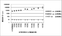
- Fig. 2 shows the results of measuring daily fluctuations for 16 days thereafter.
- the resistivity increased 24 times in 16 days to 146,702 ⁇ cm.
- Comparative Example 2 A P-type sample prepared by the same method as in Comparative Example 1 was subjected to donor killer heat treatment and treated with a 5% hydrofluoric acid aqueous solution, and immediately thereafter, the resistivity was measured by the four-point probe method, and it was 5,000 ⁇ cm. ..
- Fig. 2 shows the results of measuring daily fluctuations for 16 days thereafter.
- the resistivity increased 13 times in 16 days to 66,732 ⁇ cm.
- Comparative Example 3 A P-type sample prepared by the same method as in Comparative Example 1 and Comparative Example 2 was subjected to donor killer heat treatment and treated with a 5% hydrofluoric acid aqueous solution, and immediately thereafter, the resistivity was measured using the four-point probe method. there were.
- Fig. 2 shows the results of measuring daily fluctuations for 16 days thereafter.
- the resistivity after 16 days was 8 ⁇ cm, which decreased 0.8 times in 16 days.
- Example 1 A P-type sample prepared by the same method as in Comparative Examples 1 to 3 was subjected to donor killer heat treatment and treated with a 5% hydrofluoric acid aqueous solution. Subsequently, both surfaces of the silicon single crystal were roughly ground by #325 and then high-intensity surface grinding by #1700. Immediately after the high-intensity surface grinding, the resistivity was measured by the four-point probe method and found to be 6,889 ⁇ cm. FIG. 3 shows the result of measuring the daily fluctuation for 16 days after the high-intensity surface grinding. The resistivity after 16 days was 6,876 ⁇ cm, and the variation within 16 days was 0.2%.
- the heating and cooling in the donor killer heat treatment step can be made uniform in the silicon single crystal, and at the same time, after the donor killer heat treatment or the hydrofluoric acid treatment, the modified silicon single crystal is transformed. Since the surface of the crystal can be removed by grinding and held as a ground surface, stable resistivity measurement can be performed for a long period of time.
- the present invention is not limited to the above embodiment.
- the above-described embodiment is an exemplification, has substantially the same configuration as the technical idea described in the scope of the claims of the present invention, and any one having the same operational effect is the present invention. It is included in the technical scope of the invention.
Landscapes
- Chemical & Material Sciences (AREA)
- Health & Medical Sciences (AREA)
- Life Sciences & Earth Sciences (AREA)
- Immunology (AREA)
- Pathology (AREA)
- Physics & Mathematics (AREA)
- Analytical Chemistry (AREA)
- Biochemistry (AREA)
- General Health & Medical Sciences (AREA)
- General Physics & Mathematics (AREA)
- Engineering & Computer Science (AREA)
- Chemical Kinetics & Catalysis (AREA)
- Electrochemistry (AREA)
- Crystallography & Structural Chemistry (AREA)
- Materials Engineering (AREA)
- Metallurgy (AREA)
- Organic Chemistry (AREA)
- Biomedical Technology (AREA)
- Molecular Biology (AREA)
- Testing Or Measuring Of Semiconductors Or The Like (AREA)
- Crystals, And After-Treatments Of Crystals (AREA)
- Investigating Or Analyzing Materials By The Use Of Electric Means (AREA)
Abstract
本発明は、四探針法でシリコン単結晶の抵抗率を測定するシリコン単結晶の抵抗率測定方法において、前記シリコン単結晶の少なくとも前記抵抗率の測定を行う面を研削する第1の研削工程と、前記第1の研削工程を行ったシリコン単結晶を洗浄する洗浄工程と、前記洗浄工程を行ったシリコン単結晶を熱処理するドナーキラー熱処理工程と、前記ドナーキラー熱処理工程を行ったシリコン単結晶の少なくとも前記抵抗率の測定を行う面を研削する第2の研削工程を有し、前記第2の研削工程を行った後に四探針法で前記シリコン単結晶の抵抗率を測定するシリコン単結晶の抵抗率測定方法である。これにより、ドナーキラー熱処理後、長期間安定して測定可能なシリコン単結晶の抵抗率測定方法が提供される。
Description
本発明は、シリコン単結晶の抵抗率測定方法に関する。
四探針法を用いてシリコン単結晶の抵抗率を測定する方法は、非特許文献1(SEMI MF84-0312 “Test Method for Measuring Resistivity of Silicon Wafers with an In-line Four-point Probe”)および非特許文献2(JIS H 0602 「シリコン単結晶及びシリコンウェーハの4探針法による抵抗率測定方法」)に規定されている。
また、四探針法の測定に用いられる装置は、非特許文献3(NIST Special Publication 260-131, 2006Ed. “The Certification of 100mm Diameter Silicon Resistivity SRMs 2541 Through 2547 Using Dual-Configuration Four-Point Probe Measurements, 2006 Edition”)に記載されるNISTサンプルを用いて定期的に校正される。
また、四探針法によるシリコン単結晶抵抗率測定の前処理方法として、複数の方法が提案されている。
特許文献1は、基板の被測定面の酸化膜を除去するか又は0.5nm以下の膜厚とする処理を行った後、4時間以内に抵抗率を測定することを提案している。
また、特許文献2は、抵抗率が2000Ω・cm以上のシリコンウェーハの抵抗率の測定方法において、シリコンウェーハをドナーキラー処理した後、少なくとも2時間経過してから、非水処理により前記シリコンウェーハの被測定面の表層を厚さ10nm以上除去し、前記表層を除去した被測定面に電極針を接触させて抵抗率を測定することを提案している。
特許文献2の非水処理は例えばバフ研磨であり、そのような処理を行う理由は、ドナーキラー処理によりウェーハ表面に形成される上限膜厚が10nmの酸化膜を除去するためである。ウェーハ表層を厚さ10nm以上除去すれば、酸化膜が完全に除去され、抵抗率測定時に、測定に用いる電極とウェーハの被測定面との良好な電気的接触が得られる。
特許文献3は、接触式による物性評価および、又は非接触式による物性評価を行うための検査用ウェーハであって、前記ウェーハの検査表面が高輝度平面研削面であることを提案している。
特許文献3に開示される接触式の物性評価が四探針法による抵抗率の測定である場合、高輝度平面研削の後にドナーキラー処理を行う。
また、特許文献4は、サンプルウェーハ片に、HF:HNO3=1:5エッチング液によりエッチング処理を行い、650℃×45minまたは1100℃×60minの雰囲気でドナーキラー熱処理を行った後、表面研磨を行い、抵抗率の測定を行うことを開示している。
ドナーキラー熱処理とは、抵抗率測定の前処理として行う周知技術である。例えば特許文献3では、次のように記載されている。「抵抗率測定ではドナーキラーと呼ばれる熱処理を行う。CZ法で製造されたシリコン単結晶を450℃付近の低温でアニールすると、数個の酸素原子が集まって1個の電子(サーマルドナー)を放出する。このサーマルドナーの生成量はアニール時間に比例し増加するが、アニール温度が600℃以上になると消滅することが知られている。シリコン中でこのようなサーマルドナーが存在すると、例えばn型のシリコンでは抵抗率が見かけ上減少する。他方、p型のシリコンでは抵抗率が見かけ上増大する。」
従って、正確な抵抗率(ドーパントによる抵抗率)を評価するためには、このサーマルドナーを消滅させる必要があり、ドナーキラー熱処理を行う必要がある。熱処理では検査用ウェーハ表面に不純物が付着しているなど汚れていると熱処理炉の汚染問題が生じ、また検査用ウェーハを切り出した後に直接熱処理炉に入れると検査用ウェーハ割れの発生につながることから、熱処理の前処理としてエッチングを行う。
SEMI MF84-0312
JIS H 0602
NIST Special Publication 260-131, 2006Ed.
特許文献1は、上記のように、基板の被測定面の酸化膜を除去するか又は0.5nm以下の膜厚とする処理を行った後、4時間以内に抵抗率を測定することを提案している。特許文献1によると、放置時間が4時間程度までは抵抗率測定値が略安定するが、4時間を超えると測定値が高くなり、不安定化する。
特許文献2は、酸素原子とドーパント原子との複合体がドナーキラー処理後乖離してドーパントが再活性化するので、ドナーキラー処理後少なくとも2時間経過してからウェーハ表面を10nm以上除去して酸化膜を除去することにより、ドナーキラー処理直後の抵抗率変動を抑制することを目的としている。そのため、その実施例において、ドナーキラー処理から70時間までの抵抗率しか開示されていない。
一方、特許文献3に記載の高輝度平面研削はサンプルの表面状態を調整するためであり、ドナーキラー処理の前に行われる。
特許文献4には、ウェーハ製造工程用のインゴットブロックの径寸法よりも大きな径寸法に研削したインゴットブロックから切り出したサンプルウェーハ片にエッチング処理を行い、ドナーキラー熱処理を行った後、表面研磨を行い、抵抗率の測定を行うことが記載されている。しかし、どんな目的で、どのような表面処理が施されたのか、何ら記載がない。上記従来技術によると、ドナーキラー処理時に形成される酸化膜除去が目的であると推測される。
このように、シリコン単結晶、特に高抵抗率のシリコン単結晶で生じる、ドナーキラー熱処理直後から数日間の抵抗率変動については上記の提案があるが、ドナーキラー熱処理後一週間以上の期間に発生する抵抗率の変動に対しては何ら提案されていない。しかし、シリコン単結晶の抵抗率を保証するため、また、他のシリコン単結晶の値付けを行うため、さらにまた、シリコン単結晶の抵抗率の測定を行う測定器管理のため、抵抗率が長期間安定して測定可能な方法が必要である。
本発明は上記課題を解決するために為されたものであり、ドナーキラー熱処理後、長期間安定して測定可能なシリコン単結晶の抵抗率測定方法を提案することを目的とする。なお、本発明のシリコン単結晶は、ウェーハ形状のみならず、1/4ウェーハ等の破片形状、短冊形状、チップ形状、ブロック形状などのシリコン単結晶を含む。
上記目的を達成するために、本発明は、四探針法でシリコン単結晶の抵抗率を測定するシリコン単結晶の抵抗率測定方法において、前記シリコン単結晶の表面を研削する第1の研削工程と、前記第1の研削工程を行ったシリコン単結晶を洗浄する洗浄工程と、前記洗浄工程を行ったシリコン単結晶を熱処理するドナーキラー熱処理工程と、前記ドナーキラー熱処理工程を行ったシリコン単結晶の表面を研削する第2の研削工程を有し、前記第2の研削工程を行った後に四探針法で前記シリコン単結晶の抵抗率を測定することを特徴とするシリコン単結晶の抵抗率測定方法を提供する。
このようなシリコン単結晶の抵抗率測定方法は、ドナーキラー熱処理工程の前に第1の研削工程を有することにより、ドナーキラー熱処理工程での加熱と冷却をシリコン単結晶内で均一にすることができる。そのため、安定したドナーキラー熱処理を行うことができる。また、ドナーキラー熱処理の後に第2の研削工程を行うことにより、四探針法による抵抗率測定において探針端とシリコン単結晶の測定面における接触状態を良好にすることができる。そして、ドナーキラー熱処理後でも、シリコン単結晶の表面を研削面として保持できるので、長期間安定した測定が可能となる。このように、ドナーキラー熱処理工程の前後で第1及び第2の研削工程を有することにより、ドナーキラー熱処理後、長期間安定して測定可能なシリコン単結晶の抵抗率測定方法となる。
本発明のシリコン単結晶の抵抗率測定方法では、前記ドナーキラー熱処理工程の後に、前記シリコン単結晶をフッ酸処理するフッ酸処理工程を行い、その後に前記第2の研削工程を行うことができる。
このように、本発明では、シリコン単結晶の表面に形成された酸化膜を除去するためのフッ酸処理工程をドナーキラー熱処理工程の後、かつ第2の研削工程の前に行うことができる。
本発明のシリコン単結晶の抵抗率測定方法は、特に、前記シリコン単結晶の抵抗率が5000Ω・cm以上であるときに好適に適用することができる。
本発明のシリコン単結晶の抵抗率測定方法は、前記第2の研削工程を行った後の前記シリコン単結晶を標準サンプルとし、前記四探針法で抵抗率を測定した測定値を標準値として、他のシリコン単結晶の値付け、又は、抵抗率測定器の管理を行うことができる。
前記標準サンプルの前記標準値を再測定する際に、前記標準サンプルの表面を研削した後に四探針法で抵抗率を再測定し、該再測定値を、前記標準サンプルの新たな標準値として用いることが好ましい。
このようにすることで、より長期にわたって標準サンプルとして用いることができる。
さらに、前記第1の研削工程及び/又は前記第2の研削工程において、高輝度平面研削を行うことが好ましい。
前記第1の高輝度平面研削によりシリコン単結晶をいっそう均一な厚さに研削することができるので、ドナーキラー熱処理工程の加熱と冷却もいっそう均一になり、シリコン単結晶内のドナーキラー効果を均一にすることができる。また、前記第2の高輝度平面研削によりシリコン単結晶表面を均質に研削することができるので、抵抗率測定時に、シリコン単結晶表面状態の影響を低減することができる。
そこで、前記第1の研削工程及び前記第2の研削工程において前記高輝度平面研削を行い、前記第1の研削工程で行う高輝度平面研削において前記シリコン単結晶の両方の面を研削し、前記第2の研削工程で行う高輝度平面研削において前記シリコン単結晶の前記抵抗率の測定を行う面を研削することが望ましい。
このような方法であれば、ドナーキラー熱処理の前に第1の研削工程においてシリコン単結晶の厚さをより精度よく調整することができる。また、第2の研削工程においては、少なくとも、シリコン単結晶の抵抗率の測定を行う面を均質な高輝度研削面に調整することができる。
本発明のシリコン単結晶の抵抗測定方法によると、安定したドナーキラー熱処理を行うことができるとともに、ドナーキラー熱処理後でも、シリコン単結晶の表面を研削面として保持できるので、長期間安定した測定が可能となる。特に、高抵抗率のシリコン単結晶の抵抗率を長期間保証することができ、また、他のシリコン単結晶の値付けや、高抵抗率の測定を行う測定器管理のために使用されるサンプルの抵抗率が長期間安定して測定可能な方法となる。
以下に、本発明の実施形態を図面に基づいて説明する。
本発明は、四探針法でシリコン単結晶の抵抗率を測定するシリコン単結晶の抵抗率測定方法において、シリコン単結晶の表面を研削する第1の研削工程と、第1の研削工程を行ったシリコン単結晶を洗浄する洗浄工程と、洗浄工程を行ったシリコン単結晶を熱処理するドナーキラー熱処理工程と、ドナーキラー熱処理工程を行ったシリコン単結晶の表面を研削する第2の研削工程を有し、第2の研削工程を行った後に四探針法でシリコン単結晶の抵抗率を測定することを特徴とするシリコン単結晶の抵抗率測定方法である。
図1は、本発明の抵抗率測定方法の一例を示す概略工程図である。まず、シリコン単結晶を準備する(図1(a)シリコン単結晶の準備)。ここでは、CZ法(チョクラルスキー法)で引き上げられたインゴットの任意の位置より薄板状のウェーハをスライスし、抵抗率測定に用いるシリコン単結晶とすることができる。
次に、図1(a)で準備したシリコン単結晶の少なくとも抵抗率の測定を行う面を研削する(図1(b)第1の研削工程)。例えば、スライスされたシリコン単結晶の表面を#240~#2000番手で研削し、研削面にすることができる。特に、第1の研削工程において、高輝度平面研削(第1の高輝度平面研削工程)を行う場合は、初めに#325程度の粗い砥石を用い、シリコン単結晶の両面(主表面および裏面)を粗研削して厚さを調整した後、#1500以上の砥石を用いてさらに研削し、最終的に両面で50μm程度の高輝度平面研削を施して所望の光沢度にする。鏡面研磨の場合、片面研磨代は約10μmである。
なお、高輝度平面研削とは、当該シリコン単結晶を鏡面研磨ウェーハとした場合の光沢度を100%としたときに、70%以上の光沢度を有する高輝度面が得られるようにシリコン単結晶を研削することをいう。高輝度平面研削によって形成される研削面の光沢度は、鏡面研磨ウェーハの光沢度を100%としたときに、より好ましくは90%以上であり、98%以上とすることが特に好ましい。なお、光沢度については、試料面に対し入射角60度で評価する鏡面光沢度測定方法により測定することができる。
ドナーキラー熱処理工程よりも前に第1の研削工程を行うことにより、ドナーキラー熱処理工程での加熱と冷却をシリコン単結晶内で均一にすることができる。特に、第1の研削工程で高輝度平面研削を行うと、エッチングやラッピングに比べてシリコン単結晶の厚さをより精度よく調整することができる。そのため、ドナーキラー熱処理工程での加熱と冷却がシリコン単結晶内でより均一になり、サーマルドナーの消滅レベルも均一になるため、シリコン単結晶の抵抗率をより正確に測定することができる。
続いて、第1の研削工程を行ったシリコン単結晶を洗浄する(図1(c)洗浄工程)。例えば、アンモニア(NH3)水・過酸化水素(H2O2)水、フッ酸(HF)水・過酸化水素(H2O2)水などを用いてシリコン単結晶を洗浄することができる。この洗浄工程により、次工程のドナーキラー熱処理で用いられる熱処理炉が汚染されることを防止する。
続いて、洗浄工程を行ったシリコン単結晶を熱処理するドナーキラー熱処理工程を行う(図1(d))。このドナーキラー熱処理工程では、例えば、横型炉、縦型炉、あるいはRTP炉を用い、窒素ガス雰囲気中、650℃または1100℃でシリコン単結晶を熱処理し、酸素ドナーを消去する。
前記ドナーキラー熱処理工程で、シリコン単結晶の表面に酸化膜が形成されるので、フッ酸(HF)水溶液を用いて酸化膜を除去することができる(図1(e)フッ酸処理工程)。ただし、この酸化膜は次の第2の研削工程で除去することができるので、省略することもできる。フッ酸(HF)水溶液で処理することにより、確実に酸化膜を除去することができる。
前記ドナーキラー熱処理工程、あるいは前記フッ酸処理工程で、シリコン単結晶の表面が変質する。ドナーキラー熱処理では絶縁膜(酸化膜あるいは窒化膜)が形成され、フッ酸処理では水素イオンによりドーパントが不活性化する。そこで、ドナーキラー熱処理工程を行ったシリコン単結晶の少なくとも抵抗率の測定を行う面を研削する(図1(f)第2の研削工程)。この第2の研削工程(図1(f))を施し、変質したシリコン単結晶の表面を数μm~数十μm削り取ると共に研削面に戻す。
第2の研削工程において、高輝度平面研削(第2の高輝度平面研削工程)を行う場合は、抵抗率測定対象のシリコン単結晶の主表面(抵抗率の測定を行おうとする面)を#325程度の粗い砥石を用いた粗研削により前記シリコン単結晶の厚さを調整した後、さらに#1500以上の砥石を用いて研削し、最終的に片面20~30μmの高輝度平面研削を施して、シリコン単結晶の主表面を所望の光沢度にする。シリコン単結晶の裏面(主表面とは反対の表面)の研削は抵抗率測定に影響が無いので、不要であるが、行ってもよい。ここで、鏡面研磨面の表面粗さが約0.1nmに対し、高輝度平面研削面の表面粗さは約400nmであり、測定面に適度な凹凸があるので探針端と接触し易く、四探針法による抵抗率測定面として好適である。
第2の研削工程を高輝度平面研削にすることにより、シリコン単結晶の厚さをより均一に調整できるので、四探針法で抵抗率測定をする際、正確に厚さ補正をすることができる。
本発明では、上記のように、第1の研削工程及び第2の研削工程において高輝度平面研削を行うことが好ましい。その際、第1の研削工程で行う高輝度平面研削においてシリコン単結晶の両方の面を研削し、第2の研削工程で行う高輝度平面研削においてシリコン単結晶の抵抗率の測定を行う面を研削することが好ましい。
また、主表面が研削面のシリコン単結晶を四探針法で測定すると(図1(g)抵抗率測定工程)、探針端とシリコン単結晶の接触状態が良好なので、抵抗率の日間変動を殆ど無くすことができる。特に、シリコン単結晶の抵抗率が5000Ω・cm以上であっても抵抗率の日間変動が殆ど無く、シリコン単結晶の抵抗率保証や抵抗率測定器の管理に好適である。また、第2の研削工程まで行ったシリコン単結晶を標準サンプルとし、四探針法で抵抗率測定した測定値を標準値とすることにより、この標準サンプルの標準値を用いて、他のシリコン単結晶の抵抗率の値付けを行うことができる。
抵抗率測定器の管理としては、毎日行う日常管理と、例えば半年毎あるいは毎年行う校正があるが、どちらの管理方法でも同一のシリコン単結晶が標準サンプルとして繰り返し測定される。日常管理または校正の際に、標準サンプルに与えられた管理幅からその測定値が外れた場合、当該抵抗率測定器が異常と判断されるので、抵抗率の日間変動が殆ど無い本発明のシリコン単結晶が好適に用いられる。
ただし、標準サンプルとして同じシリコン単結晶の同じ箇所を繰り返し測定していくと、シリコン単結晶の表面への自然酸化膜形成あるいは、探針による測定箇所のダメージ等により、しだいに測定バラツキや日間変動が顕在化するようになる。そのような場合、シリコン単結晶の表面を研削し直すとよい。研削手段として、例えば高輝度平面研削を用いることができる。すなわち、標準サンプルの標準値を値付けし直しする際に、標準サンプルの表面を研削した後に四探針法で抵抗率を再測定し、該再測定値を、標準サンプルの新たな標準値として用いることができる。
高輝度平面研削を行うとシリコン単結晶が薄くなるので、サンプル厚さと抵抗率を測定し直して、標準値をつけ直すことが必要である。このようにして新たに付け直した標準値は、測定バラツキや日間変動が顕在化する前の値付け近くに戻る。
以下、実施例及び比較例を示して本発明をより具体的に説明するが、本発明は実施例に限定されるものではない。
[比較例1]
CZ法で引き上げられた直径200mm、結晶軸方位<100>のP型シリコン単結晶インゴットをスライスしたアズカットウェーハ(シリコン単結晶、以下「サンプル」)の両面を#325で粗研削した後、#1700で高輝度研削し、サンプル厚さを1200μmに調整した。
CZ法で引き上げられた直径200mm、結晶軸方位<100>のP型シリコン単結晶インゴットをスライスしたアズカットウェーハ(シリコン単結晶、以下「サンプル」)の両面を#325で粗研削した後、#1700で高輝度研削し、サンプル厚さを1200μmに調整した。
上記のようにして準備したサンプルをエタノールで脱脂した後、さらにアンモニア(NH3)水・過酸化水素(H2O2)水、フッ酸(HF)水・過酸化水素(H2O2)水を用いてサンプルを洗浄し、サンプル表面を清浄化した。
次に、サンプルを窒素雰囲気下、650℃、20分間加熱し、ドナーキラー熱処理を行った。さらに、5%フッ酸水溶液に2分間浸漬して酸化膜を除去した直後に四探針法を用いて抵抗率を測定したところ、6,000Ω・cmであった。
その後16日間の日間変動を測定した結果を図2に示した。抵抗率は16日間で24倍に上昇し、146,702Ω・cmになった。
[比較例2]
比較例1と同じ方法で準備したP型サンプルをドナーキラー熱処理し、5%フッ酸水溶液で処理した直後に四探針法を用いて抵抗率を測定したところ、5,000Ω・cmであった。
比較例1と同じ方法で準備したP型サンプルをドナーキラー熱処理し、5%フッ酸水溶液で処理した直後に四探針法を用いて抵抗率を測定したところ、5,000Ω・cmであった。
その後16日間の日間変動を測定した結果を図2に示した。抵抗率は16日間で13倍に上昇し、66,732Ω・cmになった。
[比較例3]
比較例1、比較例2と同じ方法で準備したP型サンプルをドナーキラー熱処理し、5%フッ酸水溶液で処理した直後に四探針法を用いて抵抗率を測定したところ、10Ω・cmであった。
比較例1、比較例2と同じ方法で準備したP型サンプルをドナーキラー熱処理し、5%フッ酸水溶液で処理した直後に四探針法を用いて抵抗率を測定したところ、10Ω・cmであった。
その後16日間の日間変動を測定した結果を図2に示した。16日後の抵抗率は8Ω・cmであり、16日間で0.8倍に低下した。
[実施例1]
比較例1~3と同じ方法で準備したP型サンプルをドナーキラー熱処理し、5%フッ酸水溶液で処理した。続いて、シリコン単結晶の両面を#325で粗研削した後、#1700で高輝度平面研削した。高輝度平面研削した直後に四探針法を用いて抵抗率を測定したところ、6,889Ω・cmであった。高輝度平面研削した後16日間の日間変動を測定した結果を図3に示した。16日後の抵抗率は6,876Ω・cmであり、16日間での変動は0.2%であった。
比較例1~3と同じ方法で準備したP型サンプルをドナーキラー熱処理し、5%フッ酸水溶液で処理した。続いて、シリコン単結晶の両面を#325で粗研削した後、#1700で高輝度平面研削した。高輝度平面研削した直後に四探針法を用いて抵抗率を測定したところ、6,889Ω・cmであった。高輝度平面研削した後16日間の日間変動を測定した結果を図3に示した。16日後の抵抗率は6,876Ω・cmであり、16日間での変動は0.2%であった。
本発明の抵抗率測定方法によると、ドナーキラー熱処理工程での加熱と冷却をシリコン単結晶内で均一にすることができると同時に、ドナーキラー熱処理後でも、フッ酸処理後でも、変質したシリコン単結晶の表面を研削除去するとともに、研削面として保持できるので、長期間安定した抵抗率測定が可能となる。
なお、本発明は、上記実施形態に限定されるものではない。上記実施形態は、例示であり、本発明の特許請求の範囲に記載された技術的思想と実質的に同一な構成を有し、同様な作用効果を奏するものは、いかなるものであっても本発明の技術的範囲に包含される。
Claims (7)
- 四探針法でシリコン単結晶の抵抗率を測定するシリコン単結晶の抵抗率測定方法において、
前記シリコン単結晶の表面を研削する第1の研削工程と、
前記第1の研削工程を行ったシリコン単結晶を洗浄する洗浄工程と、
前記洗浄工程を行ったシリコン単結晶を熱処理するドナーキラー熱処理工程と、
前記ドナーキラー熱処理工程を行ったシリコン単結晶の表面を研削する第2の研削工程を有し、
前記第2の研削工程を行った後に四探針法で前記シリコン単結晶の抵抗率を測定することを特徴とするシリコン単結晶の抵抗率測定方法。 - 前記ドナーキラー熱処理工程の後に、前記シリコン単結晶をフッ酸処理するフッ酸処理工程を行い、
その後に前記第2の研削工程を行うことを特徴とする請求項1に記載のシリコン単結晶の抵抗率測定方法。 - 前記シリコン単結晶の抵抗率が5000Ω・cm以上であることを特徴とする請求項1又は請求項2に記載のシリコン単結晶の抵抗率測定方法。
- 前記第2の研削工程を行った前記シリコン単結晶を標準サンプルとし、前記四探針法で抵抗率を測定した測定値を標準値として、他のシリコン単結晶の抵抗率の値付けを行い、又は、抵抗率測定器の管理を行うことを特徴とする請求項1~請求項3のいずれか1項に記載のシリコン単結晶の抵抗率測定方法。
- 前記標準サンプルの前記標準値を再測定する際に、前記標準サンプルの表面を研削した後に四探針法で抵抗率を再測定し、該再測定値を、前記標準サンプルの新たな標準値として用いることを特徴とする請求項4に記載のシリコン単結晶の抵抗率測定方法。
- 前記第1の研削工程及び/又は前記第2の研削工程において、高輝度平面研削を行うことを特徴とする請求項1~請求項5のいずれか1項に記載のシリコン単結晶の抵抗率測定方法。
- 前記第1の研削工程及び前記第2の研削工程において前記高輝度平面研削を行い、
前記第1の研削工程で行う高輝度平面研削において前記シリコン単結晶の両方の面を研削し、
前記第2の研削工程で行う高輝度平面研削において前記シリコン単結晶の前記抵抗率の測定を行う面を研削することを特徴とする請求項6に記載のシリコン単結晶の抵抗率測定方法。
Priority Applications (4)
| Application Number | Priority Date | Filing Date | Title |
|---|---|---|---|
| KR1020217027027A KR20210134633A (ko) | 2019-03-06 | 2020-01-27 | 실리콘 단결정의 저항률 측정방법 |
| DE112020000710.3T DE112020000710T5 (de) | 2019-03-06 | 2020-01-27 | Verfahren zum Messen des spezifischen Widerstands eines Silizium-Einkristalls |
| CN202080018057.8A CN113519040A (zh) | 2019-03-06 | 2020-01-27 | 单晶硅的电阻率测定方法 |
| US17/435,275 US20220146444A1 (en) | 2019-03-06 | 2020-01-27 | Method for measuring resistivity of silicon single crystal |
Applications Claiming Priority (2)
| Application Number | Priority Date | Filing Date | Title |
|---|---|---|---|
| JP2019040643A JP7172747B2 (ja) | 2019-03-06 | 2019-03-06 | シリコン単結晶の抵抗率測定方法 |
| JP2019-040643 | 2019-03-06 |
Publications (1)
| Publication Number | Publication Date |
|---|---|
| WO2020179284A1 true WO2020179284A1 (ja) | 2020-09-10 |
Family
ID=72338287
Family Applications (1)
| Application Number | Title | Priority Date | Filing Date |
|---|---|---|---|
| PCT/JP2020/002800 Ceased WO2020179284A1 (ja) | 2019-03-06 | 2020-01-27 | シリコン単結晶の抵抗率測定方法 |
Country Status (6)
| Country | Link |
|---|---|
| US (1) | US20220146444A1 (ja) |
| JP (1) | JP7172747B2 (ja) |
| KR (1) | KR20210134633A (ja) |
| CN (1) | CN113519040A (ja) |
| DE (1) | DE112020000710T5 (ja) |
| WO (1) | WO2020179284A1 (ja) |
Cited By (2)
| Publication number | Priority date | Publication date | Assignee | Title |
|---|---|---|---|---|
| JP2022181130A (ja) * | 2021-05-25 | 2022-12-07 | 株式会社Sumco | シリコンウェーハのサーマルドナー挙動予測方法及びシリコンウェーハの製造方法 |
| WO2023233834A1 (ja) * | 2022-05-31 | 2023-12-07 | 信越半導体株式会社 | 抵抗率測定方法 |
Families Citing this family (6)
| Publication number | Priority date | Publication date | Assignee | Title |
|---|---|---|---|---|
| JP7487655B2 (ja) * | 2020-12-23 | 2024-05-21 | 株式会社Sumco | シリコンウェーハの抵抗率測定方法 |
| CN113655094B (zh) * | 2021-08-06 | 2024-01-19 | 上海新昇半导体科技有限公司 | 一种确定硅片导电类型的方法 |
| CN113721076A (zh) | 2021-08-09 | 2021-11-30 | 上海新昇半导体科技有限公司 | 一种硅片电阻率的测量方法 |
| CN114999949A (zh) * | 2022-04-08 | 2022-09-02 | 上海新昇半导体科技有限公司 | 电阻率测试的标准片的制备方法、标准片及校准方法 |
| CN117038428B (zh) * | 2023-06-19 | 2025-01-07 | 宁夏中欣晶圆半导体科技有限公司 | 改善硅片电阻率性能的预处理方法 |
| JP7552942B1 (ja) | 2024-01-29 | 2024-09-18 | 信越半導体株式会社 | シリコン単結晶の抵抗率測定方法 |
Citations (6)
| Publication number | Priority date | Publication date | Assignee | Title |
|---|---|---|---|---|
| JP2000243731A (ja) * | 1999-02-18 | 2000-09-08 | Mitsubishi Materials Silicon Corp | 高平坦度ウェーハの製造方法 |
| JP2001015459A (ja) * | 1999-06-30 | 2001-01-19 | Mitsubishi Materials Silicon Corp | 両面研磨ウェーハの製造方法 |
| JP2001118902A (ja) * | 1999-10-15 | 2001-04-27 | Shin Etsu Handotai Co Ltd | 検査用ウェーハ、その作成方法、及びそれを用いた検査方法 |
| JP2002076080A (ja) * | 2000-08-31 | 2002-03-15 | Shin Etsu Handotai Co Ltd | 半導体シリコン基板の抵抗率測定方法、半導体シリコン基板の導電型判定方法、及び半導体シリコン基板の製造方法 |
| JP2015026755A (ja) * | 2013-07-29 | 2015-02-05 | グローバルウェーハズ・ジャパン株式会社 | シリコンウェーハの抵抗率測定方法 |
| JP2018032771A (ja) * | 2016-08-25 | 2018-03-01 | 信越半導体株式会社 | 抵抗率標準サンプルの製造方法及びエピタキシャルウェーハの抵抗率測定方法 |
Family Cites Families (4)
| Publication number | Priority date | Publication date | Assignee | Title |
|---|---|---|---|---|
| US6180867B1 (en) * | 1996-04-17 | 2001-01-30 | General Electric Company | Thermal sensor array and methods of fabrication and use |
| JP5003987B2 (ja) * | 2001-08-08 | 2012-08-22 | 信越半導体株式会社 | サンプルウェーハの検査方法及び検査装置並びに検査装置の管理方法 |
| JP2014082316A (ja) * | 2012-10-16 | 2014-05-08 | Shin Etsu Handotai Co Ltd | Soiウェーハの製造方法 |
| JP6332422B1 (ja) | 2016-12-05 | 2018-05-30 | 株式会社Sumco | シリコンウェーハの製造方法 |
-
2019
- 2019-03-06 JP JP2019040643A patent/JP7172747B2/ja active Active
-
2020
- 2020-01-27 DE DE112020000710.3T patent/DE112020000710T5/de not_active Withdrawn
- 2020-01-27 WO PCT/JP2020/002800 patent/WO2020179284A1/ja not_active Ceased
- 2020-01-27 CN CN202080018057.8A patent/CN113519040A/zh not_active Withdrawn
- 2020-01-27 US US17/435,275 patent/US20220146444A1/en not_active Abandoned
- 2020-01-27 KR KR1020217027027A patent/KR20210134633A/ko not_active Withdrawn
Patent Citations (6)
| Publication number | Priority date | Publication date | Assignee | Title |
|---|---|---|---|---|
| JP2000243731A (ja) * | 1999-02-18 | 2000-09-08 | Mitsubishi Materials Silicon Corp | 高平坦度ウェーハの製造方法 |
| JP2001015459A (ja) * | 1999-06-30 | 2001-01-19 | Mitsubishi Materials Silicon Corp | 両面研磨ウェーハの製造方法 |
| JP2001118902A (ja) * | 1999-10-15 | 2001-04-27 | Shin Etsu Handotai Co Ltd | 検査用ウェーハ、その作成方法、及びそれを用いた検査方法 |
| JP2002076080A (ja) * | 2000-08-31 | 2002-03-15 | Shin Etsu Handotai Co Ltd | 半導体シリコン基板の抵抗率測定方法、半導体シリコン基板の導電型判定方法、及び半導体シリコン基板の製造方法 |
| JP2015026755A (ja) * | 2013-07-29 | 2015-02-05 | グローバルウェーハズ・ジャパン株式会社 | シリコンウェーハの抵抗率測定方法 |
| JP2018032771A (ja) * | 2016-08-25 | 2018-03-01 | 信越半導体株式会社 | 抵抗率標準サンプルの製造方法及びエピタキシャルウェーハの抵抗率測定方法 |
Cited By (5)
| Publication number | Priority date | Publication date | Assignee | Title |
|---|---|---|---|---|
| JP2022181130A (ja) * | 2021-05-25 | 2022-12-07 | 株式会社Sumco | シリコンウェーハのサーマルドナー挙動予測方法及びシリコンウェーハの製造方法 |
| JP7582070B2 (ja) | 2021-05-25 | 2024-11-13 | 株式会社Sumco | シリコンウェーハのサーマルドナー挙動予測方法及びシリコンウェーハの製造方法 |
| WO2023233834A1 (ja) * | 2022-05-31 | 2023-12-07 | 信越半導体株式会社 | 抵抗率測定方法 |
| JP2023176764A (ja) * | 2022-05-31 | 2023-12-13 | 信越半導体株式会社 | 抵抗率測定方法 |
| JP7704074B2 (ja) | 2022-05-31 | 2025-07-08 | 信越半導体株式会社 | 抵抗率測定方法 |
Also Published As
| Publication number | Publication date |
|---|---|
| KR20210134633A (ko) | 2021-11-10 |
| US20220146444A1 (en) | 2022-05-12 |
| DE112020000710T5 (de) | 2021-11-18 |
| JP2020145306A (ja) | 2020-09-10 |
| JP7172747B2 (ja) | 2022-11-16 |
| CN113519040A (zh) | 2021-10-19 |
Similar Documents
| Publication | Publication Date | Title |
|---|---|---|
| JP7172747B2 (ja) | シリコン単結晶の抵抗率測定方法 | |
| CN101765901B (zh) | 贴合晶片的制造方法 | |
| JP5572085B2 (ja) | Soiウェーハの製造方法 | |
| US7993452B2 (en) | Method of manufacturing epitaxial silicon wafer | |
| TW201007865A (en) | Silicon single crystal wafer, process for producing silicon single crystal wafer, and method for evaluating silicon single crystal wafer | |
| KR20190048278A (ko) | 실리콘 웨이퍼의 산화물층의 두께 예측 방법 | |
| JP2020528392A (ja) | 裏側にピットを有するリン化インジウムウエハ、ならびに、それを製造するための方法およびエッチング液 | |
| JP4600707B2 (ja) | 半導体シリコン基板の抵抗率測定方法、半導体シリコン基板の導電型判定方法、及び半導体シリコン基板の製造方法 | |
| JP2015026755A (ja) | シリコンウェーハの抵抗率測定方法 | |
| KR100925359B1 (ko) | 에피택셜 웨이퍼 및 그 제조 방법 | |
| JP3593195B2 (ja) | SiC単結晶基板の製造方法 | |
| KR100733443B1 (ko) | 실리콘 부재 및 그 제조 방법 | |
| JP2012114138A (ja) | シリコンウェーハのエピタキシャル成長方法 | |
| JP2001118902A (ja) | 検査用ウェーハ、その作成方法、及びそれを用いた検査方法 | |
| JP2012204369A (ja) | エピタキシャルウェーハの製造方法 | |
| JP4603677B2 (ja) | アニールウェーハの製造方法及びアニールウェーハ | |
| KR100969161B1 (ko) | 에피텍셜 웨이퍼 비저항 표준 샘플 제조방법 및 이방법으로 제조된 비저항 표준 샘플을 이용한 비저항 측정장비 보정 방법 | |
| CN107706122B (zh) | 一种退火工艺的检测方法 | |
| TWI737339B (zh) | 單結晶矽的電阻率測定方法 | |
| JP3896919B2 (ja) | シリコンウエーハのNi汚染の評価方法 | |
| TWI814488B (zh) | 高電阻矽晶圓的厚度測量方法以及平坦度測量方法 | |
| JP5742739B2 (ja) | 金属汚染評価用シリコン基板の選別方法 | |
| KR20260072241A (ko) | 고저항 실리콘 단결정의 저항률 측정 방법 | |
| JP7347318B2 (ja) | 貼り合わせsoiウェーハのベースウェーハの抵抗率測定方法 | |
| JP4305800B2 (ja) | シリコンウエハ表面の窒化物評価方法 |
Legal Events
| Date | Code | Title | Description |
|---|---|---|---|
| 121 | Ep: the epo has been informed by wipo that ep was designated in this application |
Ref document number: 20765827 Country of ref document: EP Kind code of ref document: A1 |
|
| ENP | Entry into the national phase |
Ref document number: 20217027027 Country of ref document: KR Kind code of ref document: A |
|
| 122 | Ep: pct application non-entry in european phase |
Ref document number: 20765827 Country of ref document: EP Kind code of ref document: A1 |