WO2020171006A1 - 半導体基板の製造方法及び組成物 - Google Patents
半導体基板の製造方法及び組成物 Download PDFInfo
- Publication number
- WO2020171006A1 WO2020171006A1 PCT/JP2020/006003 JP2020006003W WO2020171006A1 WO 2020171006 A1 WO2020171006 A1 WO 2020171006A1 JP 2020006003 W JP2020006003 W JP 2020006003W WO 2020171006 A1 WO2020171006 A1 WO 2020171006A1
- Authority
- WO
- WIPO (PCT)
- Prior art keywords
- group
- carbon atoms
- compound
- film
- formula
- Prior art date
Links
Classifications
-
- C—CHEMISTRY; METALLURGY
- C08—ORGANIC MACROMOLECULAR COMPOUNDS; THEIR PREPARATION OR CHEMICAL WORKING-UP; COMPOSITIONS BASED THEREON
- C08G—MACROMOLECULAR COMPOUNDS OBTAINED OTHERWISE THAN BY REACTIONS ONLY INVOLVING UNSATURATED CARBON-TO-CARBON BONDS
- C08G77/00—Macromolecular compounds obtained by reactions forming a linkage containing silicon with or without sulfur, nitrogen, oxygen or carbon in the main chain of the macromolecule
- C08G77/60—Macromolecular compounds obtained by reactions forming a linkage containing silicon with or without sulfur, nitrogen, oxygen or carbon in the main chain of the macromolecule in which all the silicon atoms are connected by linkages other than oxygen atoms
-
- G—PHYSICS
- G03—PHOTOGRAPHY; CINEMATOGRAPHY; ANALOGOUS TECHNIQUES USING WAVES OTHER THAN OPTICAL WAVES; ELECTROGRAPHY; HOLOGRAPHY
- G03F—PHOTOMECHANICAL PRODUCTION OF TEXTURED OR PATTERNED SURFACES, e.g. FOR PRINTING, FOR PROCESSING OF SEMICONDUCTOR DEVICES; MATERIALS THEREFOR; ORIGINALS THEREFOR; APPARATUS SPECIALLY ADAPTED THEREFOR
- G03F7/00—Photomechanical, e.g. photolithographic, production of textured or patterned surfaces, e.g. printing surfaces; Materials therefor, e.g. comprising photoresists; Apparatus specially adapted therefor
- G03F7/004—Photosensitive materials
- G03F7/075—Silicon-containing compounds
-
- G—PHYSICS
- G03—PHOTOGRAPHY; CINEMATOGRAPHY; ANALOGOUS TECHNIQUES USING WAVES OTHER THAN OPTICAL WAVES; ELECTROGRAPHY; HOLOGRAPHY
- G03F—PHOTOMECHANICAL PRODUCTION OF TEXTURED OR PATTERNED SURFACES, e.g. FOR PRINTING, FOR PROCESSING OF SEMICONDUCTOR DEVICES; MATERIALS THEREFOR; ORIGINALS THEREFOR; APPARATUS SPECIALLY ADAPTED THEREFOR
- G03F7/00—Photomechanical, e.g. photolithographic, production of textured or patterned surfaces, e.g. printing surfaces; Materials therefor, e.g. comprising photoresists; Apparatus specially adapted therefor
- G03F7/20—Exposure; Apparatus therefor
-
- G—PHYSICS
- G03—PHOTOGRAPHY; CINEMATOGRAPHY; ANALOGOUS TECHNIQUES USING WAVES OTHER THAN OPTICAL WAVES; ELECTROGRAPHY; HOLOGRAPHY
- G03F—PHOTOMECHANICAL PRODUCTION OF TEXTURED OR PATTERNED SURFACES, e.g. FOR PRINTING, FOR PROCESSING OF SEMICONDUCTOR DEVICES; MATERIALS THEREFOR; ORIGINALS THEREFOR; APPARATUS SPECIALLY ADAPTED THEREFOR
- G03F7/00—Photomechanical, e.g. photolithographic, production of textured or patterned surfaces, e.g. printing surfaces; Materials therefor, e.g. comprising photoresists; Apparatus specially adapted therefor
- G03F7/26—Processing photosensitive materials; Apparatus therefor
- G03F7/36—Imagewise removal not covered by groups G03F7/30 - G03F7/34, e.g. using gas streams, using plasma
Definitions
- the present invention relates to a semiconductor substrate manufacturing method and composition.
- a resist process in which a resist film laminated on a substrate is exposed and developed with a developing solution and the substrate is etched by using the obtained resist pattern as a mask is used for forming a pattern of a semiconductor element or the like (Japanese Patent Laid-Open No. 2004-2004). 310019 and WO 2012/0393337).
- the exposure light to be used is KrF excimer laser light (248 nm) and ArF excimer laser light (193 nm), extreme ultraviolet rays (13.5 nm, EUV), electron beam (EB). The wavelength tends to be shortened.
- the present invention has been made based on the above circumstances, and an object thereof is to provide a semiconductor substrate on which a pattern can be formed by a method other than a method using a liquid such as an alkali developing solution or an organic solvent developing solution. It is to provide a manufacturing method and a composition.
- composition (I) a composition containing a metal or a semimetal
- coating a substrate
- processing step a step of applying a composition containing a metal or a semimetal (hereinafter, also referred to as “composition (I)”) directly or indirectly to a substrate
- film (I) a film containing a metal or a semimetal
- exposure step a step of exposing a film containing a metal or a semimetal formed by the coating step with an electron beam or extreme ultraviolet rays
- exposure step a step of removing the exposed or unexposed portion of the exposed film with plasma or ion gas
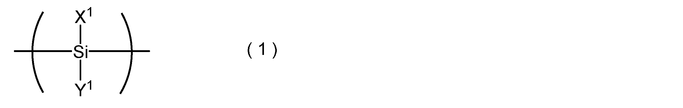
- compositions used for forming a film for removing exposed portions or unexposed portions by plasma or ion gas after electron beam or extreme ultraviolet exposure A composition comprising a compound having as a repeating unit at least one structural unit selected from the group consisting of a structural unit represented by the formula (1) and a structural unit represented by the following formula (2), and a solvent: is there.
- X 1 and Y 1 are each independently a hydrogen atom, a hydroxy group, a halogen atom or a monovalent organic group having 1 to 20 carbon atoms.
- R 1 is a divalent hydrocarbon group having 1 to 20 carbon atoms.
- X 2 and Y 2 are each independently a hydrogen atom, a hydroxy group, a halogen atom or 1 carbon atom. It is a monovalent organic group of up to 20.
- a fine pattern with few defects can be formed by a method other than a method using a liquid such as an alkali developing solution or an organic solvent developing solution. Therefore, these can be suitably used for manufacturing semiconductor devices, which are expected to be further miniaturized in the future.
- the manufacturing method of the semiconductor substrate includes a coating step, an exposing step, and a removing step.
- the semiconductor substrate manufacturing method by including the above steps, it is possible to form a fine pattern with few defects by a method other than a method using a liquid such as an alkali developing solution or an organic solvent developing solution.
- a liquid such as an alkali developing solution or an organic solvent developing solution.
- This change in physical properties causes a difference in the removal rate of the exposed portion and the unexposed portion due to the plasma or ion gas, so that either the exposed portion or the unexposed portion can be removed, and as a result, fine defects with few defects can be removed. It is possible to form various patterns.
- the method for manufacturing a semiconductor substrate may include a step of forming an organic underlayer film directly or indirectly on the substrate (hereinafter, also referred to as “organic underlayer film forming step”) before the coating step. Further, after the removing step, a step of etching the substrate using the pattern formed by the removing step as a mask (hereinafter, also referred to as “substrate etching step”) may be provided. Each step will be described below.
- Organic underlayer film forming step In this step, the organic underlayer film is formed directly or indirectly on the substrate. By this step, specifically, the organic underlayer film is formed on the substrate directly or through another layer.
- the substrate examples include a silicon wafer, an insulating film of silicon oxide, silicon nitride, silicon oxynitride, polysiloxane, etc., and a resin substrate.
- a wafer coated with a low dielectric insulating film formed of "Black Diamond” manufactured by AMAT, "Silk” manufactured by Dow Chemical, "LKD5109” manufactured by JSR Corporation, or the like can be used.
- a substrate on which a pattern such as a wiring groove (trench) or a plug groove (via) is formed may be used as the substrate.
- the organic underlayer film is different from the film (I) formed from the composition (I).
- the organic underlayer film may contain a silicon atom.
- the organic underlayer film has a predetermined function (for example, antireflection property) required in order to further supplement the function of the film (I) or to obtain the function that the film (I) does not have in the pattern formation. It is a film that imparts coating film flatness and high etching resistance to fluorine-based gas.
- Examples of the organic lower layer film include an antireflection film and the like.
- Examples of the antireflection film-forming composition include "NFC HM8006" by JSR Corporation.
- the organic underlayer film can be formed by applying a composition for forming an organic underlayer film by a spin coating method or the like to form a coating film, and then heating it.
- the coating step is performed after the organic underlayer film forming step. That is, in the coating step, the composition (I) is directly or indirectly applied to the organic underlayer film formed in the organic underlayer film forming step.
- composition (I) is applied directly or indirectly to the substrate.
- the coating film of the composition (I) is formed on the substrate directly or through another layer such as the organic underlayer film.
- the composition (I) will be described later.
- the method of applying the composition (I) is not particularly limited, and examples thereof include known methods such as spin coating.
- a film (I) containing a metal or a semimetal is usually formed by heating and curing a coating film formed from the composition (I).
- the lower limit of the temperature for heating the coating film is preferably 90°C, more preferably 120°C, and even more preferably 140°C.
- the upper limit of the temperature is preferably 550°C, more preferably 450°C, and even more preferably 350°C.
- the heating can be performed, for example, in a nitrogen atmosphere or an air atmosphere.
- the lower limit of the average thickness of the formed film (I) is preferably 1 nm, more preferably 3 nm, further preferably 5 nm.
- the upper limit of the average thickness is preferably 1,000 nm, more preferably 500 nm, even more preferably 100 nm.
- the film (I) formed in the above coating step is exposed to an electron beam or extreme ultraviolet rays. This exposure is performed by selectively irradiating the film (I) with an electron beam or extreme ultraviolet rays. Thereby, the exposed part and the unexposed part of the exposed film (I) are obtained.
- Examples of the method of exposing with an electron beam include a method using an electron beam drawing apparatus (for example, "HL800D” manufactured by Hitachi, Ltd.).
- the lower limit of the exposure dose of the electron beam is preferably 20 ⁇ C / cm 2, 40 ⁇ C / cm 2 is more preferable.
- the upper limit of the exposure dose is preferably 1,000 ⁇ C / cm 2, 800 ⁇ C / cm 2 is more preferable.
- extreme ultraviolet rays for example, an EUV scanner (for example, "TWINSCAN NXE:3300B" (NA0.3, Sigma 0.9) of ASML, etc.) is used, and extreme ultraviolet rays (wavelength: 13.5 nm) are masked. And the like, for example, a method of selectively irradiating.
- the lower limit of the exposure of extreme ultraviolet preferably 5mJ / cm 2, 10mJ / cm 2 is more preferable.
- the upper limit of the exposure dose 500 mJ/cm 2 is preferable, and 400 mJ/cm 2 is more preferable.
- the exposed or unexposed portion of the exposed film (I) is removed by plasma or ion gas. More specifically, the exposed part and the unexposed part of the exposed film (I) are exposed to plasma or ion gas. Since the exposed part and the unexposed part of the exposed film (I) have different removal rates by plasma or ion gas, one of the exposed part and the unexposed part can be removed from the substrate. Pattern is formed. When the removal rate of the exposed part of the exposed film (I) is faster than the removal rate of the unexposed part of the exposed film (I), a positive pattern by the unexposed part of the exposed film (I) Is obtained. When the removal rate of the exposed part of the exposed film (I) is slower than the removal rate of the unexposed part of the exposed film (I), the negative pattern of the exposed part of the exposed film (I) is can get.
- Plasma refers to plasma of various gases.
- plasma examples include oxygen plasma, ozone plasma, nitrogen plasma, hydrogen plasma, chlorine plasma, fluorine plasma, helium plasma, neon plasma, argon plasma, krypton plasma, xenon plasma, and ammonia plasma. Of these, chlorine plasma or fluorine plasma is preferable.
- Examples of the method for exposing the plasma include a method using an etching apparatus (for example, “NLD-6000” manufactured by ULVAC, Inc.).
- the etching gas to be used can be appropriately selected depending on the elemental composition of the film (I) and the like.
- chlorine gas or fluorine gas is usually used as the etching gas.
- the conditions for plasma exposure are usually a gas flow rate of 20 cc/min or more and 100 cc/min or less, and a supply power of 50 W or more and 1,500 W or less.
- the lower limit of the plasma exposure time is preferably 5 seconds, more preferably 10 seconds.
- the upper limit of the time is preferably 10 minutes, more preferably 5 minutes.
- Ion gas means a gas containing ions.
- the above “plasma” also corresponds to “ion gas” when it contains ions.
- the ions contained in the ion gas include, for example, nitrogen ions, helium ions, neon ions, argon ions, krypton ions, xenon ions, and helium ions.
- a method of exposing to ion gas for example, a method using an ion irradiation device, a method using an etching device, etc. can be mentioned.
- the lower limit of the exposure time of the ion gas is preferably 5 seconds, more preferably 10 seconds.
- the upper limit of the time is preferably 10 minutes, more preferably 5 minutes.
- the substrate is etched using the pattern of the film (I) formed in the removing step as a mask. More specifically, etching is performed one or more times using the pattern of the film (I) formed in the removal step as a mask to obtain a patterned substrate.
- a step of etching the organic underlayer film using the pattern of the film (I) as a mask is provided.
- a pattern is formed on the substrate by etching the substrate using the organic underlayer film pattern formed in the organic underlayer film etching step as a mask.
- the etching may be dry etching or wet etching, but dry etching is preferable. Dry etching for forming a pattern on the organic underlayer film can be performed using a known dry etching apparatus.
- the etching gas used for dry etching can be appropriately selected depending on the elemental composition of the film (I) and the organic underlayer film to be etched, and for example, CHF 3 , CF 4 , C 2 F 6 , C 3 F.
- fluorine-based gas such as SF 6 , chlorine-based gas such as Cl 2 , BCl 3 , oxygen-based gas such as O 2 , O 3 , H 2 O, H 2 , NH 3 , CO, CH 4 , C 2 H 2 , C 2 H 4 , C 2 H 6 , C 3 H 4 , C 3 H 6 , C 3 H 8 , HF, HI, HBr, HCl, NO, NH 3 , reductive gas such as BCl 3 , He, An inert gas such as N 2 or Ar is used, and these gases can also be mixed and used. Oxygen-based gas is usually used for dry etching of the organic underlayer film using the film (I) pattern as a mask.
- oxygen-based gas such as O 2 , O 3 , H 2 O, H 2 , NH 3 , CO, CH 4 , C 2 H 2 , C 2 H 4 , C 2 H 6 , C 3 H 4 , C 3 H 6 , C 3
- Dry etching when etching the substrate using the organic underlayer film pattern as a mask can be performed using a known dry etching apparatus.
- the etching gas used for the dry etching can be appropriately selected depending on the elemental composition of the organic underlayer film and the substrate to be etched, and is similar to those exemplified as the etching gas used for the dry etching of the organic underlayer film, for example. Etching gas and the like.
- the etching may be performed by using different etching gases a plurality of times.
- composition (I) is a composition containing a metal or a metalloid.
- Examples of the metal include metals belonging to Groups 2 to 16 of the periodic table.
- Examples of Group 2 metals include beryllium, magnesium, calcium, strontium, and barium.
- Examples of Group 3 metals include metals belonging to lanthanoids such as scandium, yttrium, and lanthanum, and metals belonging to actinides such as actinium.
- Examples of Group 4 metals include titanium, zirconium, and hafnium.
- Examples of the Group 5 metal include vanadium, niobium, tantalum, and the like.
- Examples of the Group 6 metal include chromium, molybdenum, and tungsten.
- Examples of Group 7 metals include manganese and rhenium.
- Group 8 metals iron, ruthenium, osmium, etc.
- Examples of Group 9 metals include cobalt, rhodium, and iridium
- the Group 10 metals include nickel, palladium, platinum, Examples of Group 11 metals include copper, silver, and gold.
- Group 12 metals include zinc, cadmium, mercury, etc.
- Examples of Group 13 metals include aluminum, gallium, indium, and thallium.
- Examples of Group 14 metals include tin and lead, Examples of Group 15 metals include bismuth Examples of the Group 16 metal include polonium and the like.
- Examples of semimetals include boron, silicon, germanium, arsenic, antimony, tellurium, and astatine.
- the composition (I) usually contains a compound containing a metal or a metalloid (hereinafter, also referred to as “[A] compound”) and a solvent (hereinafter, also referred to as “[B] solvent”).
- the composition (I) may contain, in addition to the compound [A] and the solvent [B], other components as long as the effects of the present invention are not impaired.
- each component will be described.
- the compound [A] is a compound containing a metal or a metalloid.
- Examples of the [A] compound include a metal-containing compound and a semimetal-containing compound.
- Examples of the semimetal-containing compound include silicon-containing compounds.
- Specific examples of the silicon-containing compound include, for example, a structural unit represented by the following formula (1) (hereinafter, also referred to as “structural unit (I)”) and a structural unit represented by the following formula (2) (
- structural unit (II) a structural unit represented by the following formula (1)
- a compound having at least one structural unit selected from the group consisting of "structural unit (II)" as a repeating unit (hereinafter, also referred to as "[A1] compound” can be mentioned.
- the compound [A1] has the structural unit (I) and/or the structural unit (II) as a repeating unit.
- the upper limit of the total number is, for example, 50, preferably 40, and more preferably 30.
- the compound [A1] may have, in addition to the structural unit (I) and the structural unit (II), other structural units as long as the effects of the present invention are not impaired.
- each structural unit will be described.
- the structural unit (I) is a structural unit represented by the following formula (1).
- the Si atom in the following formula (1) is usually bonded to the Si atom in the adjacent structural unit.
- X 1 and Y 1 are each independently a hydrogen atom, a hydroxy group, a halogen atom or a monovalent organic group having 1 to 20 carbon atoms.
- Organic group refers to a group containing at least one carbon atom.
- Examples of the monovalent organic group having 1 to 20 carbon atoms represented by X 1 and Y 1 include a monovalent hydrocarbon group having 1 to 20 carbon atoms, and a divalent carbon-carbon group of the above hydrocarbon group.
- Monovalent group ( ⁇ ) containing a hetero atom-containing group a monovalent group ( ⁇ ) in which a part or all of the hydrogen atoms of the above hydrocarbon group and group ( ⁇ ) are replaced with a monovalent hetero atom-containing group.
- Examples of the monovalent hydrocarbon group having 1 to 20 carbon atoms include a monovalent chain hydrocarbon group having 1 to 20 carbon atoms, a monovalent alicyclic hydrocarbon group having 3 to 20 carbon atoms, and 6 carbon atoms. Examples include monovalent aromatic hydrocarbon groups of 20 to 20.
- Examples of the monovalent chain hydrocarbon group having 1 to 20 carbon atoms include chain chains such as alkanes such as methane, ethane, propane and butane, alkenes such as ethene, propene and butene, and alkynes such as ethyne, propyne and butyne. Examples thereof include groups excluding one hydrogen atom contained in hydrocarbon.
- Examples of the monovalent alicyclic hydrocarbon group having 3 to 20 carbon atoms include cycloalkanes such as cyclopentane and cyclohexane, and alicyclic saturated hydrocarbons such as bridged ring saturated hydrocarbons such as norbornane, adamantane and tricyclodecane. Hydrogen, cyclopentene, cyclohexene and other cycloalkenes, norbornene, tricyclodecene and other bridged ring unsaturated hydrocarbons and other alicyclic unsaturated hydrocarbons and other alicyclic hydrocarbons, excluding one hydrogen atom Groups and the like.
- the monovalent aromatic hydrocarbon group having 6 to 20 carbon atoms is, for example, one on the aromatic ring or alkyl group of an arene such as benzene, toluene, ethylbenzene, xylene, naphthalene, methylnaphthalene, anthracene or methylanthracene.
- hetero atom constituting the divalent or monovalent hetero atom-containing group
- oxygen atom nitrogen atom, sulfur atom, phosphorus atom, silicon atom, halogen atom and the like.
- divalent hetero atom-containing group examples include -O-, -CO-, -S-, -CS-, -NR'-, and groups in which two or more of these are combined.
- R' is a hydrogen atom or a monovalent chain hydrocarbon group. Among these, -O- or -S- is preferable, and -O- is more preferable.
- Examples of the monovalent hetero atom-containing group include halogen atoms such as fluorine atom, chlorine atom, bromine atom and iodine atom, hydroxy group, carboxy group, cyano group, amino group and sulfanyl group.
- R A is a hydrogen atom or a monovalent organic group having 1 to 20 carbon atoms.
- the monovalent organic group having 1 to 20 carbon atoms represented by R A is preferably a monovalent chain organic group having 1 to 20 carbon atoms.
- the “chain organic group” includes both a straight chain organic group and a branched chain organic group. Examples of the monovalent chain organic group having 1 to 20 carbon atoms include chain groups among the groups exemplified as the monovalent organic group having 1 to 20 carbon atoms of X 1 and Y 1. ..
- R A a hydrogen atom or a monovalent chain hydrocarbon group having 1 to 20 carbon atoms is preferable, a hydrogen atom or a monovalent chain hydrocarbon group having 1 to 6 carbon atoms is more preferable, and a hydrogen atom or carbon atom.
- the alkyl groups of the numbers 1 to 6 are more preferable, and the methyl group or the ethyl group is particularly preferable.
- R A is a hydrogen atom or a monovalent organic group having 1 to 20 carbon atoms.
- the monovalent organic group having 1 to 20 carbon atoms represented by R A is preferably a monovalent chain organic group having 1 to 20 carbon atoms. Examples of the monovalent chain organic group having 1 to 20 carbon atoms include chain groups among the groups exemplified as the monovalent organic group having 1 to 20 carbon atoms of X 1 and Y 1. ..
- R A a hydrogen atom or a monovalent chain hydrocarbon group having 1 to 20 carbon atoms is preferable, a hydrogen atom or a monovalent chain hydrocarbon group having 1 to 6 carbon atoms is more preferable, and a hydrogen atom or carbon atom.
- the alkyl groups of the numbers 1 to 6 are more preferable, and the methyl group or the ethyl group is particularly preferable.
- structural unit (I) examples include structural units represented by the following formulas (1-1) to (1-15) (hereinafter, also referred to as “structural units (I-1) to (I-15)”) and the like. Is mentioned.
- the structural unit (I) is preferably structural unit (I-1), (I-2), (I-6) or (I-10).
- the lower limit of the content ratio of the structural unit (I) 1 mol% is preferable, 10 mol% is more preferable, 50 mol% is further preferable, and 70 mol% is based on all structural units constituting the [A1] compound. Is particularly preferable, 90 mol% is even more preferable, and 100 mol% is the most preferable.
- the content ratio (mol %) of each structural unit of the [A1] compound is usually the same as the molar ratio of the monomer that gives each structural unit used in the synthesis of the [A1] compound.
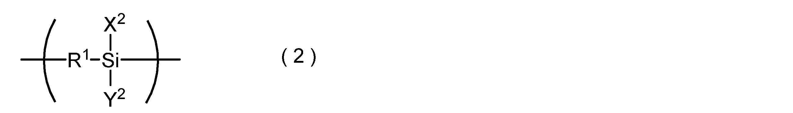
- the structural unit (II) is a structural unit represented by the following formula (2).
- R 1 in the following formula (2) is usually bonded to the Si atom in the adjacent structural unit.
- R 1 is a divalent hydrocarbon group having 1 to 20 carbon atoms.
- X 2 and Y 2 are each independently a hydrogen atom, a hydroxy group, a halogen atom or a monovalent organic group having 1 to 20 carbon atoms.
- Examples of the divalent hydrocarbon group having 1 to 20 carbon atoms represented by R 1 include a divalent aliphatic hydrocarbon group having 1 to 20 carbon atoms and a divalent aromatic hydrocarbon group having 6 to 20 carbon atoms. Groups and the like.
- Examples of the divalent aliphatic hydrocarbon group having 1 to 20 carbon atoms include a divalent chain hydrocarbon group having 1 to 20 carbon atoms and a divalent alicyclic hydrocarbon group having 3 to 20 carbon atoms. Can be mentioned.
- the divalent chain hydrocarbon group having 1 to 20 carbon atoms is a group obtained by removing one hydrogen atom from the monovalent chain hydrocarbon group having 1 to 20 carbon atoms exemplified as the above X 1 and Y 1. Etc.
- As the divalent alicyclic hydrocarbon group having 3 to 20 carbon atoms one hydrogen atom is excluded from the monovalent alicyclic hydrocarbon group having 3 to 20 carbon atoms exemplified as the above X 1 and Y 1. And the like.
- divalent aromatic hydrocarbon group having 6 to 20 carbon atoms for example, one hydrogen atom is removed from the monovalent aromatic hydrocarbon group having 6 to 20 carbon atoms exemplified as the above X 1 and Y 1 . Groups and the like.
- R 1 is preferably a divalent aliphatic hydrocarbon group having 1 to 20 carbon atoms or a divalent aromatic hydrocarbon group having 6 to 20 carbon atoms, and a divalent aliphatic hydrocarbon group having 1 to 20 carbon atoms A group is more preferable, a divalent chain hydrocarbon group having 1 to 20 carbon atoms is further preferable, and a methanediyl group or an ethanediyl group is particularly preferable.
- Examples of the monovalent organic group having 1 to 20 carbon atoms represented by X 2 and Y 2 include the same groups as those exemplified above as the monovalent organic group having 1 to 20 carbon atoms for X 1 and Y 1. Etc.
- R B is a hydrogen atom or a monovalent organic group having 1 to 20 carbon atoms.
- the monovalent organic group having 1 to 20 carbon atoms represented by R B is preferably a monovalent chain organic group having 1 to 20 carbon atoms. Examples of the monovalent chain organic group having 1 to 20 carbon atoms include chain groups among the groups exemplified as the monovalent organic group having 1 to 20 carbon atoms of X 1 and Y 1. ..
- R B a hydrogen atom or a monovalent chain hydrocarbon group having 1 to 20 carbon atoms is preferable, a hydrogen atom or a monovalent chain hydrocarbon group having 1 to 6 carbon atoms is more preferable, and a hydrogen atom or carbon atom.
- the alkyl groups of the numbers 1 to 6 are more preferable, and the methyl group or the ethyl group is particularly preferable.
- the structural unit (II) is a structural unit in which R 1 of the above formula (2) is a divalent chain hydrocarbon group having 1 to 20 carbon atoms or a divalent aromatic hydrocarbon group having 6 to 20 carbon atoms. Is more preferable, and a structural unit in which R 1 in the above formula (2) is a divalent chain hydrocarbon group having 1 to 10 carbon atoms or a divalent aromatic hydrocarbon group having 6 to 10 carbon atoms is more preferable, and A structural unit in which R 1 in the formula (2) is an alkanediyl group having 1 to 6 carbon atoms or an arenediyl group having 6 to 10 carbon atoms is more preferable, and R 1 in the above formula (2) is a methanediyl group, an ethanediyl group or benzene. Structural units that are diyl groups are particularly preferred.
- the lower limit of the content ratio of the structural unit (II) 1 mol% is preferable, 10 mol% is more preferable, 50 mol% is further preferable, and 70 mol% is based on all the structural units constituting the [A1] compound. Is particularly preferable, 90 mol% is even more preferable, and 100 mol% is the most preferable.
- the upper limit of the content ratio of the other structural units is preferably 20 mol% and more preferably 10 mol% with respect to all the structural units constituting the [A1] compound. preferable.
- the lower limit of the content ratio is, for example, 0.1 mol %.
- the lower limit of the polystyrene reduced weight average molecular weight (Mw) of the compound [A] is preferably 300, more preferably 700, further preferably 1,000, and particularly preferably 1,300.
- Mw polystyrene reduced weight average molecular weight
- 100,000 is preferable, 10,000 is more preferable, 5,000 is further preferable, and 3,000 is particularly preferable.
- a GPC column (two "G2000HXL”, one "G3000HXL” and one “G4000HXL” from Tosoh Corporation) is used, and a flow rate: 1.0 mL/min, an elution solvent: tetrahydrofuran, It is a value measured by gel permeation chromatography (detector: differential refractometer) using monodisperse polystyrene as a standard under analysis conditions of column temperature: 40°C.
- the lower limit of the content ratio of the [A] compound is preferably 30% by mass, more preferably 50% by mass, further preferably 80% by mass, particularly preferably 90% by mass, based on all components other than the [B] solvent. ..
- the upper limit of the content ratio may be 100% by mass.
- the lower limit of the content ratio of the [A] compound in the composition (I) is preferably 0.1% by mass, more preferably 0.3% by mass, further preferably 0.5% by mass, and particularly preferably 1% by mass. ..
- the upper limit of the content ratio is preferably 50% by mass, more preferably 30% by mass, further preferably 20% by mass, and particularly preferably 10% by mass.
- the compound [A] may be used alone or in combination of two or more.
- the solvent [B] is not particularly limited as long as it is a solvent that can dissolve or disperse the compound [A] and other optional components.
- Examples of the [B] solvent include alcohol solvents, ketone solvents, ether solvents, ester solvents, nitrogen-containing solvents, water and the like.
- the solvent [B] one type or two or more types can be used.
- alcohol solvents include monoalcohol solvents such as methanol, ethanol, n-propanol, iso-propanol, n-butanol, and iso-butanol, ethylene glycol, 1,2-propylene glycol, diethylene glycol, dipropylene glycol, etc.
- monoalcohol solvents such as methanol, ethanol, n-propanol, iso-propanol, n-butanol, and iso-butanol, ethylene glycol, 1,2-propylene glycol, diethylene glycol, dipropylene glycol, etc.
- polyhydric alcohol solvents examples include polyhydric alcohol solvents.
- ketone-based solvent examples include acetone, methyl ethyl ketone, methyl-n-propyl ketone, methyl-iso-butyl ketone, cyclohexanone and the like.
- ether solvents include ethyl ether, iso-propyl ether, ethylene glycol dibutyl ether, diethylene glycol monomethyl ether, diethylene glycol monoethyl ether, diethylene glycol diethyl ether, propylene glycol monomethyl ether, propylene glycol monoethyl ether, propylene glycol monopropyl ether, Tetrahydrofuran etc. are mentioned.
- ester solvents include ethyl acetate, ⁇ -butyrolactone, n-butyl acetate, ethylene glycol monomethyl ether acetate, ethylene glycol monoethyl ether acetate, diethylene glycol monomethyl ether acetate, diethylene glycol monoethyl ether acetate, propylene glycol monomethyl ether acetate, and acetic acid.
- Examples include propylene glycol monoethyl ether, dipropylene glycol monomethyl ether acetate, dipropylene glycol monoethyl ether acetate, ethyl propionate, n-butyl propionate, methyl lactate, ethyl lactate and the like.
- nitrogen-containing solvent examples include N,N-dimethylformamide, N,N-dimethylacetamide, N-methylpyrrolidone and the like.
- ether-based solvents and/or ester-based solvents are preferable, and ether-based solvents and/or ester-based solvents having a glycol structure are more preferable because they have excellent film-forming properties.
- Examples of the ether solvent and ester solvent having a glycol structure include propylene glycol monomethyl ether, propylene glycol monoethyl ether, propylene glycol monopropyl ether, propylene glycol monomethyl ether acetate, propylene glycol monoethyl ether acetate, and propylene glycol monopropyl acetate.
- Examples include ether and the like. Of these, propylene glycol monomethyl ether acetate is particularly preferable.
- the lower limit of the content of the glycol-structured ether solvent and ester solvent in the solvent [B] is preferably 20% by mass, more preferably 60% by mass, further preferably 90% by mass, and particularly preferably 100% by mass. ..
- the lower limit of the content of the [B] solvent is preferably 100 parts by mass, more preferably 500 parts by mass, further preferably 1,000 parts by mass, and 5,000 parts by mass with respect to 100 parts by mass of the [A] compound. Is particularly preferable.
- the upper limit of the content is preferably 100,000 parts by mass, more preferably 50,000 parts by mass, further preferably 20,000 parts by mass, and particularly preferably 15,000 parts by mass.
- the lower limit of the content ratio of the [B] solvent in the composition (I) is preferably 50% by mass, more preferably 70% by mass, and further preferably 90% by mass. As a maximum of the above-mentioned content rate, 99.9 mass% is preferred and 99.5 mass% is more preferred.
- Other components include, for example, acid generators, basic compounds (including base generators), radical generators, surfactants, colloidal silica, colloidal alumina, organic polymers and the like. Each of the other components may be used alone or in combination of two or more.
- composition (I) is prepared by mixing, for example, a solution of the compound [A] and a solvent [B] with other components at a predetermined ratio, and the resulting mixed solution is preferably 0.2 ⁇ m or less in pore size. It can be prepared by filtering with a filter or the like.
- composition (I) a composition containing a metal or metalloid in the coating step of the method for manufacturing a semiconductor substrate described above.
- a film (film (I)) containing the above metal or metalloid is formed. It is considered that the physical properties of this film (I) are changed in the exposed portion by exposing it with an electron beam or extreme ultraviolet rays.
- the composition can be preferably used in the above-mentioned method for manufacturing the semiconductor substrate.
- composition is described as the composition (I) used in the coating step of the above-mentioned semiconductor substrate manufacturing method.
- the weight average molecular weight (Mw), the concentration of the compound [A] in the solution, and the average thickness of the film in this example were measured by the following methods.
- the parts by weight are the total weight of the monomers used or the weight of the solution of the compound (a) in diisopropyl ether is 100 parts by weight. Means the value of the case.
- the mol% means a value when the total number of mols of Si in the monomers used is 100 mol %.
- the polymerization reaction was carried out at 40° C. for 1 hour and then at 60° C. for 3 hours, with the completion of the dropping as the reaction start time.
- tetrahydrofuran (213 parts by mass) was added, and the polymerization solution was ice-cooled and cooled to 10°C or lower.
- methanol 150 mol% was added dropwise from the dropping funnel over 10 minutes while stirring.
- the reaction was carried out at 20° C. for 1 hour, with the end of dropping being the start time of the reaction.
- the polymerization solution was poured into diisopropyl ether (700 parts by mass), and the precipitated salt was filtered off.
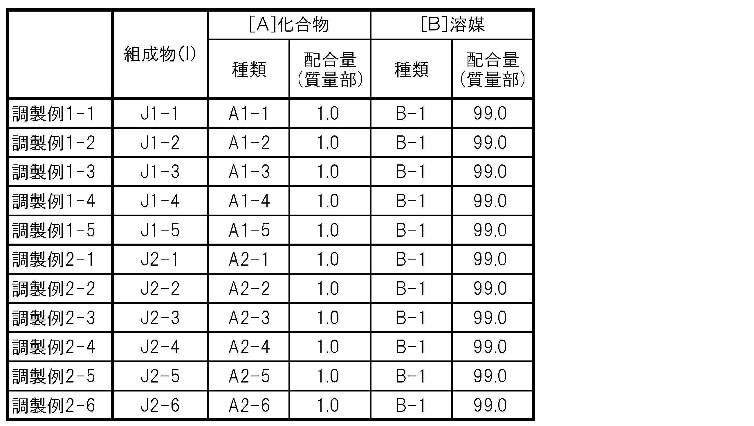
- composition (I) ⁇ Preparation of composition (I)>
- the [A] compound and the [B] solvent used for the preparation of the composition (I) are shown below.
- Table 4 shows measured values (nm/min) of the chlorine-based gas etching rate and the fluorine-based gas etching rate when the film (I) was subjected to electron beam exposure and when not subjected to exposure.
- the etching rate remarkably differs depending on whether the film (I) formed from the composition (I) is exposed to an electron beam. Therefore, according to the method for manufacturing a semiconductor substrate, the exposed portion or the unexposed portion of the film (I) can be removed, and a fine pattern with few defects can be formed.
- a fine pattern with few defects can be formed by a method other than a method using a liquid such as an alkali developing solution or an organic solvent developing solution. Therefore, these can be suitably used for manufacturing semiconductor devices, which are expected to be further miniaturized in the future.
Landscapes
- Physics & Mathematics (AREA)
- General Physics & Mathematics (AREA)
- Chemical & Material Sciences (AREA)
- Health & Medical Sciences (AREA)
- Chemical Kinetics & Catalysis (AREA)
- Medicinal Chemistry (AREA)
- Polymers & Plastics (AREA)
- Organic Chemistry (AREA)
- Materials For Photolithography (AREA)
Abstract
アルカリ現像液や有機溶媒現像液などの液体を用いる方法以外の方法によりパターンを形成することができる半導体基板の製造方法の提供を目的とする。本発明は、基板に直接又は間接に金属又は半金属を含有する組成物を塗工する工程と、上記塗工工程により形成された金属又は半金属を含有する膜を電子線又は極端紫外線で露光する工程と、上記露光された膜の露光部又は未露光部をプラズマ又はイオンガスにより除去する工程とを備える半導体基板の製造方法である。上記組成物が、下記式(1)で表される構造単位及び下記式(2)で表される構造単位からなる群より選ばれる少なくとも1種の構造単位を繰り返し単位として有する化合物と、溶媒とを含有することが好ましい。
Description
本発明は、半導体基板の製造方法及び組成物に関する。
半導体素子等のパターン形成には、基板上に積層されたレジスト膜を露光及び現像液で現像し、得られたレジストパターンをマスクとして基板をエッチングするレジストプロセスが用いられている(特開2004-310019号公報及び国際公開第2012/039337号参照)。近年、半導体デバイスの高集積化が進んでおり、使用する露光光はKrFエキシマレーザー光(248nm)及びArFエキシマレーザー光(193nm)から、極端紫外線(13.5nm、EUV)、電子線(EB)へと短波長化される傾向にある。
レジスト膜をEUVで露光するEUVリソグラフィーにおいては、パターンサイズが10nm以下にまで微細化すると、アルカリ現像液や有機溶媒現像液では、レジストパターンを形成することが難しいという不都合があると考えられる。また、レジスト膜の一部がアルカリ現像液や有機溶媒現像液に溶解しなかったり、アルカリ現像液や有機溶媒現像液に溶解したレジスト膜の一部が基板に付着するなどして、欠陥が生じやすいという不都合があると考えられる。
本発明は、以上のような事情に基づいてなされたものであり、その目的は、アルカリ現像液や有機溶媒現像液などの液体を用いる方法以外の方法によりパターンを形成することができる半導体基板の製造方法及び組成物を提供することにある。
上記課題を解決するためになされた発明は、基板に直接又は間接に金属又は半金属を含有する組成物(以下、「組成物(I)」ともいう)を塗工する工程(以下、「塗工工程」ともいう)と、上記塗工工程により形成された金属又は半金属を含有する膜(以下、「膜(I)」ともいう)を電子線又は極端紫外線で露光する工程(以下、「露光工程」ともいう)と、上記露光された膜の露光部又は未露光部をプラズマ又はイオンガスにより除去する工程(以下、「除去工程」ともいう)とを備える半導体基板の製造方法である。
上記課題を解決するためになされた別の発明は、電子線又は極端紫外線露光後に露光部又は未露光部をプラズマ又はイオンガスにより除去するための膜の形成に用いられる組成物であって、下記式(1)で表される構造単位及び下記式(2)で表される構造単位からなる群より選ばれる少なくとも1種の構造単位を繰り返し単位として有する化合物と、溶媒とを含有する組成物である。

(式(1)中、X1及びY1は、それぞれ独立して、水素原子、ヒドロキシ基、ハロゲン原子又は炭素数1~20の1価の有機基である。)

(式(2)中、R1は、炭素数1~20の2価の炭化水素基である。X2及びY2は、それぞれ独立して、水素原子、ヒドロキシ基、ハロゲン原子又は炭素数1~20の1価の有機基である。)
本発明の半導体基板の製造方法及び組成物によれば、アルカリ現像液や有機溶媒現像液などの液体を用いる方法以外の方法により欠陥の少ない微細なパターンを形成することができる。従って、これらは今後さらに微細化が進行すると予想される半導体デバイスの製造等に好適に用いることができる。
<半導体基板の製造方法>
当該半導体基板の製造方法は、塗工工程と、露光工程と、除去工程とを備える。
当該半導体基板の製造方法は、塗工工程と、露光工程と、除去工程とを備える。
当該半導体基板の製造方法によれば、上記各工程を備えることで、アルカリ現像液や有機溶媒現像液などの液体を用いる方法以外の方法により欠陥の少ない微細なパターンを形成することができる。当該半導体基板の製造方法が上記構成を備えることで、上記効果を奏する理由については必ずしも明確ではないが、例えば以下のように推察することができる。すなわち、組成物(I)から形成される膜(I)は、電子線又は極端紫外線で露光することにより、露光部において物性が変化すると考えられる。この物性の変化により、露光部及び未露光部のプラズマ又はイオンガスによる除去速度に差が生じるので、露光部及び未露光部のいずれか一方を除去することができ、その結果、欠陥の少ない微細なパターンを形成することができる。
当該半導体基板の製造方法は、塗工工程の前に、基板に直接又は間接に有機下層膜を形成する工程(以下、「有機下層膜形成工程」ともいう)を備えていてもよい。また、除去工程の後に、除去工程により形成されたパターンをマスクとして基板をエッチングする工程(以下、「基板エッチング工程」ともいう)を備えていてもよい。
以下、各工程について説明する。
以下、各工程について説明する。
[有機下層膜形成工程]
本工程では、基板に直接又は間接に有機下層膜を形成する。本工程により、具体的には、基板に直接又は他の層を介して有機下層膜が形成される。
本工程では、基板に直接又は間接に有機下層膜を形成する。本工程により、具体的には、基板に直接又は他の層を介して有機下層膜が形成される。
基板としては、例えばシリコンウェハ、酸化シリコン、窒化シリコン、酸窒化シリコン、ポリシロキサン等の絶縁膜、樹脂基板等が挙げられる。基板として、例えばAMAT社の「ブラックダイヤモンド」、ダウケミカル社の「シルク」、JSR(株)の「LKD5109」等により形成される低誘電体絶縁膜で被覆したウェハなどを使用することができる。また、基板として、配線溝(トレンチ)、プラグ溝(ビア)等のパターンが形成された基板を用いてもよい。
有機下層膜は、組成物(I)から形成される膜(I)とは異なるものである。但し、有機下層膜は、ケイ素原子を含有していてもよい。有機下層膜は、パターン形成において、膜(I)が有する機能をさらに補ったり、膜(I)が有していない機能を得るために、必要とされる所定の機能(例えば、反射防止性、塗工膜平坦性、フッ素系ガスに対する高エッチング耐性)を付与したりする膜のことである。
有機下層膜としては、例えば反射防止膜等が挙げられる。反射防止膜形成用組成物としては、例えばJSR(株)の「NFC HM8006」等が挙げられる。
有機下層膜は、有機下層膜形成用組成物を回転塗工法等により塗工して塗膜を形成した後、加熱すること等により形成することができる。
当該半導体基板の製造方法において、有機下層膜形成工程を行う場合、有機下層膜形成工程の後に、塗工工程を行う。すなわち、塗工工程において、有機下層膜形成工程により形成された有機下層膜に直接又は間接に組成物(I)を塗工する。
[塗工工程]
本工程では、基板に直接又は間接に組成物(I)を塗工する。本工程により、基板に直接又は有機下層膜等の他の層を介して組成物(I)の塗膜が形成される。組成物(I)については後述する。
本工程では、基板に直接又は間接に組成物(I)を塗工する。本工程により、基板に直接又は有機下層膜等の他の層を介して組成物(I)の塗膜が形成される。組成物(I)については後述する。
組成物(I)の塗工方法は特に限定されないが、例えば回転塗工法等の公知の方法が挙げられる。
組成物(I)から形成された塗膜を、通常、加熱して硬化等させることにより、金属又は半金属を含有する膜(I)が形成される。
塗膜を加熱する際の温度の下限としては、90℃が好ましく、120℃がより好ましく、140℃がさらに好ましい。上記温度の上限としては、550℃が好ましく、450℃がより好ましく、350℃がさらに好ましい。上記加熱は、例えば窒素雰囲気下、大気雰囲気下等で行うことができる。形成される膜(I)の平均厚みの下限としては、1nmが好ましく、3nmがより好ましく、5nmがさらに好ましい。上記平均厚みの上限としては、1,000nmが好ましく、500nmがより好ましく、100nmがさらに好ましい。
[露光工程]
本工程では、上記塗工工程により形成された膜(I)を電子線又は極端紫外線で露光する。この露光は、膜(I)に選択的に電子線又は極端紫外線を照射して行う。これにより、露光された膜(I)の露光部と未露光部とが得られる。
本工程では、上記塗工工程により形成された膜(I)を電子線又は極端紫外線で露光する。この露光は、膜(I)に選択的に電子線又は極端紫外線を照射して行う。これにより、露光された膜(I)の露光部と未露光部とが得られる。
電子線で露光する方法としては、例えば電子線描画装置(例えば(株)日立製作所の「HL800D」等)などを用いる方法などが挙げられる。電子線の露光量の下限としては、20μC/cm2が好ましく、40μC/cm2がより好ましい。上記露光量の上限としては、1,000μC/cm2が好ましく、800μC/cm2がより好ましい。
極端紫外線で露光する方法としては、例えばEUVスキャナー(例えばASML社の「TWINSCAN NXE:3300B」(NA0.3、シグマ0.9)等)などを用い、極端紫外線(波長:13.5nm)をマスク等により選択的に照射する方法などが挙げられる。極端紫外線の露光量の下限としては、5mJ/cm2が好ましく、10mJ/cm2がより好ましい。上記露光量の上限としては、500mJ/cm2が好ましく、400mJ/cm2がより好ましい。
[除去工程]
本工程では、上記露光された膜(I)の露光部又は未露光部をプラズマ又はイオンガスにより除去する。より具体的には、上記露光された膜(I)の露光部及び未露光部に対し、プラズマ又はイオンガスの暴露を行う。露光された膜(I)の露光部と未露光部とでプラズマ又はイオンガスによる除去速度が異なることによって、露光部及び未露光部の一方を基板から除去することができるので、膜(I)のパターンが形成される。露光された膜(I)の未露光部の除去速度よりも露光された膜(I)の露光部の除去速度が速い場合は、露光された膜(I)の未露光部によるポジ型のパターンが得られる。露光された膜(I)の未露光部の除去速度よりも露光された膜(I)の露光部の除去速度が遅い場合は、露光された膜(I)の露光部によるネガ型のパターンが得られる。
本工程では、上記露光された膜(I)の露光部又は未露光部をプラズマ又はイオンガスにより除去する。より具体的には、上記露光された膜(I)の露光部及び未露光部に対し、プラズマ又はイオンガスの暴露を行う。露光された膜(I)の露光部と未露光部とでプラズマ又はイオンガスによる除去速度が異なることによって、露光部及び未露光部の一方を基板から除去することができるので、膜(I)のパターンが形成される。露光された膜(I)の未露光部の除去速度よりも露光された膜(I)の露光部の除去速度が速い場合は、露光された膜(I)の未露光部によるポジ型のパターンが得られる。露光された膜(I)の未露光部の除去速度よりも露光された膜(I)の露光部の除去速度が遅い場合は、露光された膜(I)の露光部によるネガ型のパターンが得られる。
「プラズマ」とは、各種ガスをプラズマ化したものをいう。
プラズマとしては、例えば酸素プラズマ、オゾンプラズマ、窒素プラズマ、水素プラズマ、塩素プラズマ、フッ素プラズマ、ヘリウムプラズマ、ネオンプラズマ、アルゴンプラズマ、クリプトンプラズマ、キセノンプラズマ、アンモニアプラズマ等が挙げられる。これらの中で、塩素プラズマ又はフッ素プラズマが好ましい。
プラズマの暴露を行う方法としては、例えばエッチング装置(例えば(株)アルバックの「NLD-6000」)を用いる方法等が挙げられる。使用するエッチングガスとしては、膜(I)の元素組成等により、適宜選択することができ、例えばCHF3、CF4、C2F6、C3F8、SF6等のフッ素系ガス、Cl2、BCl3等の塩素系ガス、O2、O3、H2O等の酸素系ガス、H2、NH3、CO、CH4、C2H2、C2H4、C2H6、C3H4、C3H6、C3H8、HF、HI、HBr、HCl、NO、NH3、BCl3等の還元性ガス、He、N2、Ar等の不活性ガスなどを用いることができる。これらのガスは混合して用いることもできる。膜(I)がケイ素含有膜である場合、エッチングガスとしては、通常、塩素系ガス又はフッ素系ガスが用いられる。
プラズマの暴露の条件としては、通常、ガス流量が20cc/min以上100cc/min以下、供給電力が50W以上1,500W以下である。
プラズマの暴露の時間の下限としては、5秒が好ましく、10秒がより好ましい。上記時間の上限としては、10分が好ましく、5分がより好ましい。
「イオンガス」とは、イオンを含有する気体をいう。上記「プラズマ」は、イオンを含有する場合、「イオンガス」にも該当する。
イオンガスが含有するイオンとしては、例えば窒素イオン、ヘリウムイオン、ネオンイオン、アルゴンイオン、クリプトンイオン、キセノンイオン、ヘリウムイオン等が挙げられる。
イオンガスの暴露を行う方法としては、例えばイオン照射装置を用いる方法、エッチング装置を用いる方法等が挙げられる。
イオンガスの暴露の時間の下限としては、5秒が好ましく、10秒がより好ましい。上記時間の上限としては、10分が好ましく、5分がより好ましい。
[基板エッチング工程]
本工程では、除去工程により形成された膜(I)のパターンをマスクとして、基板をエッチングする。より具体的には、除去工程により形成された膜(I)のパターンをマスクとした1又は複数回のエッチングを行って、パターニングされた基板を得る。
本工程では、除去工程により形成された膜(I)のパターンをマスクとして、基板をエッチングする。より具体的には、除去工程により形成された膜(I)のパターンをマスクとした1又は複数回のエッチングを行って、パターニングされた基板を得る。
基板に有機下層膜を形成した場合には、膜(I)のパターンをマスクとして有機下層膜をエッチングする工程を備える。有機下層膜エッチング工程により形成された有機下層膜パターンをマスクとして基板をエッチングすることにより、基板にパターンを形成する。
上記エッチングは、ドライエッチングでもウェットエッチングでもよいが、ドライエッチングが好ましい。有機下層膜にパターンを形成する際のドライエッチングは、公知のドライエッチング装置を用いて行うことができる。ドライエッチングに使用するエッチングガスとしては、膜(I)及びエッチングされる有機下層膜の元素組成等により、適宜選択することができ、例えば、CHF3、CF4、C2F6、C3F8、SF6等のフッ素系ガス、Cl2、BCl3等の塩素系ガス、O2、O3、H2O等の酸素系ガス、H2、NH3、CO、CH4、C2H2、C2H4、C2H6、C3H4、C3H6、C3H8、HF、HI、HBr、HCl、NO、NH3、BCl3等の還元性ガス、He、N2、Ar等の不活性ガス等が用いられ、これらのガスは混合して用いることもできる。膜(I)パターンをマスクとした有機下層膜のドライエッチングには、通常、酸素系ガスが用いられる。
有機下層膜パターンをマスクとして基板をエッチングする際のドライエッチングは、公知のドライエッチング装置を用いて行うことができる。ドライエッチングに使用するエッチングガスとしては、有機下層膜及びエッチングされる基板の元素組成等により、適宜選択することができ、例えば上記有機下層膜のドライエッチングに用いられるエッチングガスとして例示したものと同様のエッチングガス等が挙げられる。複数回の異なるエッチングガスにより、エッチングを行ってもよい。
上記除去工程をエッチング装置を用いて行った場合、基板エッチング工程における有機下層膜及び基板をエッチングする方法としてドライエッチングを採用することにより、これらの工程を同一の装置を用いて行うことができ、より欠陥の少ない微細なパターニングされた基板を得ることができる。
次に、組成物(I)について説明する。
次に、組成物(I)について説明する。
[組成物(I)]
組成物(I)は、金属又は半金属を含有する組成物である。
組成物(I)は、金属又は半金属を含有する組成物である。
金属としては、例えば周期表第2族~第16族に属する金属等が挙げられる。
第2族の金属としては、例えばベリリウム、マグネシウム、カルシウム、ストロンチウム、バリウム等が、
第3族の金属としては、例えばスカンジウム、イットリウム、ランタン等のランタノイドに属する金属、アクチニウム等のアクチノイドに属する金属などが、
第4族の金属としては、例えばチタン、ジルコニウム、ハフニウム等が、
第5族の金属としては、例えばバナジウム、ニオブ、タンタル等が、
第6族の金属としては、例えばクロム、モリブデン、タングステン等が、
第7族の金属としては、マンガン、レニウム等が、
第8族の金属としては、鉄、ルテニウム、オスミウム等が、
第9族の金属としては、コバルト、ロジウム、イリジウム等が、
第10族の金属としては、ニッケル、パラジウム、白金等が、
第11族の金属としては、銅、銀、金等が、
第12族の金属としては、亜鉛、カドミウム、水銀等が、
第13族の金属としては、アルミニウム、ガリウム、インジウム、タリウム等が、
第14族の金属としては、スズ、鉛等が、
第15族の金属としては、ビスマス等が、
第16族の金属としては、ポロニウム等が挙げられる。
半金属としては、例えばホウ素、ケイ素、ゲルマニウム、ヒ素、アンチモン、テルル、アスタチン等が挙げられる。
組成物(I)は、通常、金属又は半金属を含有する化合物(以下、「[A]化合物」ともいう)と、溶媒(以下、「[B]溶媒」)ともいう)とを含有する。組成物(I)は、[A]化合物及び[B]溶媒以外に、本発明の効果を損なわない範囲において、その他の成分を含有していてもよい。
以下、各成分について説明する。
以下、各成分について説明する。
([A]化合物)
[A]化合物は、金属又は半金属を含有する化合物である。
[A]化合物は、金属又は半金属を含有する化合物である。
[A]化合物としては、例えば金属含有化合物、半金属含有化合物等が挙げられる。半金属含有化合物としては、例えばケイ素含有化合物等が挙げられる。ケイ素含有化合物の具体例としては、例えば後述する式(1)で表される構造単位(以下、「構造単位(I)」ともいう)及び後述する下記式(2)で表される構造単位(以下、「構造単位(II)」ともいう)からなる群より選ばれる少なくとも1種の構造単位を繰り返し単位として有する化合物(以下、「[A1]化合物」ともいう)等が挙げられる。
[A1]化合物は、構造単位(I)及び/又は構造単位(II)を繰り返し単位として有する。[A1]化合物が有する構造単位(I)及び構造単位(II)の合計数の下限としては、2であり、5が好ましく、10がさらに好ましく、15が特に好ましい。上記合計数の上限としては、例えば50であり、40が好ましく、30がより好ましい。
[A1]化合物は、構造単位(I)及び構造単位(II)以外に、本発明の効果を損なわない範囲において、その他の構造単位を有していてもよい。
以下、各構造単位について説明する。
以下、各構造単位について説明する。
(構造単位(I))
構造単位(I)は、下記式(1)で表される構造単位である。下記式(1)中のSi原子は、通常、隣接する構造単位中のSi原子に結合している。
構造単位(I)は、下記式(1)で表される構造単位である。下記式(1)中のSi原子は、通常、隣接する構造単位中のSi原子に結合している。
上記式(1)中、X1及びY1は、それぞれ独立して、水素原子、ヒドロキシ基、ハロゲン原子又は炭素数1~20の1価の有機基である。
「有機基」とは、少なくとも1個の炭素原子を含む基をいう。X1及びY1で表される炭素数1~20の1価の有機基としては、例えば炭素数1~20の1価の炭化水素基、上記炭化水素基の炭素-炭素間に2価のヘテロ原子含有基を含む1価の基(α)、上記炭化水素基及び基(α)が有する水素原子の一部又は全部を1価のヘテロ原子含有基で置換した1価の基(β)、上記炭化水素基、基(α)又は基(β)と2価のヘテロ原子含有基とを組み合わせた1価の基(γ)などが挙げられる。
炭素数1~20の1価の炭化水素基としては、例えば炭素数1~20の1価の鎖状炭化水素基、炭素数3~20の1価の脂環式炭化水素基、炭素数6~20の1価の芳香族炭化水素基等が挙げられる。
炭素数1~20の1価の鎖状炭化水素基としては、例えばメタン、エタン、プロパン、ブタン等のアルカン、エテン、プロペン、ブテン等のアルケン、エチン、プロピン、ブチン等のアルキンなどの鎖状炭化水素が有する1個の水素原子を除いた基等が挙げられる。
炭素数3~20の1価の脂環式炭化水素基としては、例えばシクロペンタン、シクロヘキサン等のシクロアルカン、ノルボルナン、アダマンタン、トリシクロデカン等の橋かけ環飽和炭化水素などの脂環式飽和炭化水素、シクロペンテン、シクロヘキセン等のシクロアルケン、ノルボルネン、トリシクロデセン等の橋かけ環不飽和炭化水素などの脂環式不飽和炭化水素などの脂環式炭化水素が有する1個の水素原子を除いた基などが挙げられる。
炭素数6~20の1価の芳香族炭化水素基としては、例えばベンゼン、トルエン、エチルベンゼン、キシレン、ナフタレン、メチルナフタレン、アントラセン、メチルアントラセン等のアレーンが有する芳香環上又はアルキル基上の1個の水素原子を除いた基などが挙げられる。
2価又は1価のヘテロ原子含有基を構成するヘテロ原子としては、例えば酸素原子、窒素原子、硫黄原子、リン原子、ケイ素原子、ハロゲン原子等が挙げられる。
2価のヘテロ原子含有基としては、例えば-O-、-CO-、-S-、-CS-、-NR’-、これらのうちの2つ以上を組み合わせた基等が挙げられる。R’は、水素原子又は1価の鎖状炭化水素基である。これらの中で、-O-又は-S-が好ましく、-O-がより好ましい。
1価のヘテロ原子含有基としては、例えばフッ素原子、塩素原子、臭素原子、ヨウ素原子等のハロゲン原子、ヒドロキシ基、カルボキシ基、シアノ基、アミノ基、スルファニル基等が挙げられる。
X1としては、-ORAが好ましい。RAは、水素原子又は炭素数1~20の1価の有機基である。RAで表される炭素数1~20の1価の有機基としては、炭素数1~20の1価の鎖状の有機基が好ましい。「鎖状の有機基」には、直鎖状の有機基及び分岐鎖状の有機基の両方が含まれる。炭素数1~20の1価の鎖状の有機基としては、例えば上記X1及びY1の炭素数1~20の1価の有機基として例示した基のうち鎖状の基等が挙げられる。RAとしては、水素原子又は炭素数1~20の1価の鎖状炭化水素基が好ましく、水素原子又は炭素数1~6の1価の鎖状炭化水素基がより好ましく、水素原子又は炭素数1~6のアルキル基がさらに好ましく、メチル基又はエチル基が特に好ましい。
Y1としては、-ORAが好ましい。RAは、水素原子又は炭素数1~20の1価の有機基である。RAで表される炭素数1~20の1価の有機基としては、炭素数1~20の1価の鎖状の有機基が好ましい。炭素数1~20の1価の鎖状の有機基としては、例えば上記X1及びY1の炭素数1~20の1価の有機基として例示した基のうち鎖状の基等が挙げられる。RAとしては、水素原子又は炭素数1~20の1価の鎖状炭化水素基が好ましく、水素原子又は炭素数1~6の1価の鎖状炭化水素基がより好ましく、水素原子又は炭素数1~6のアルキル基がさらに好ましく、メチル基又はエチル基が特に好ましい。
構造単位(I)としては、例えば下記式(1-1)~(1-15)で表される構造単位(以下、「構造単位(I-1)~(I-15)」ともいう)等が挙げられる。


構造単位(I)としては、構造単位(I-1)、(I-2)、(I-6)又は(I-10)が好ましい。
構造単位(I)の含有割合の下限としては、[A1]化合物を構成する全構造単位に対して、1モル%が好ましく、10モル%がより好ましく、50モル%がさらに好ましく、70モル%が特に好ましく、90モル%がさらに特に好ましく、100モル%が最も好ましい。構造単位(I)の含有割合を上記範囲とすることで、当該半導体基板の製造方法によれば、より欠陥の少ない微細なパターンを形成することができる。なお、[A1]化合物の各構造単位の含有割合(モル%)は、通常[A1]化合物の合成に用いた各構造単位を与える単量体のモル比率と同等になる。
(構造単位(II))
構造単位(II)は、下記式(2)で表される構造単位である。下記式(2)中のR1は、通常、隣接する構造単位中のSi原子に結合している。
構造単位(II)は、下記式(2)で表される構造単位である。下記式(2)中のR1は、通常、隣接する構造単位中のSi原子に結合している。

上記式(2)中、R1は、炭素数1~20の2価の炭化水素基である。X2及びY2は、それぞれ独立して、水素原子、ヒドロキシ基、ハロゲン原子又は炭素数1~20の1価の有機基である。
R1で表される炭素数1~20の2価の炭化水素基としては、例えば炭素数1~20の2価の脂肪族炭化水素基、炭素数6~20の2価の芳香族炭化水素基等が挙げられる。
炭素数1~20の2価の脂肪族炭化水素基としては、例えば炭素数1~20の2価の鎖状炭化水素基、炭素数3~20の2価の脂環式炭化水素基等が挙げられる。炭素数1~20の2価の鎖状炭化水素基としては、上記X1及びY1として例示した炭素数1~20の1価の鎖状炭化水素基から1個の水素原子を除いた基等が挙げられる。炭素数3~20の2価の脂環式炭化水素基としては、上記X1及びY1として例示した炭素数3~20の1価の脂環式炭化水素基から1個の水素原子を除いた基等が挙げられる。炭素数6~20の2価の芳香族炭化水素基としては、例えば上記X1及びY1として例示した炭素数6~20の1価の芳香族炭化水素基から1個の水素原子を除いた基等が挙げられる。
R1としては、炭素数1~20の2価の脂肪族炭化水素基又は炭素数6~20の2価の芳香族炭化水素基が好ましく、炭素数1~20の2価の脂肪族炭化水素基がより好ましく、炭素数1~20の2価の鎖状炭化水素基がさらに好ましく、メタンジイル基又はエタンジイル基が特に好ましい。
X2及びY2で表される炭素数1~20の1価の有機基としては、例えば上記X1及びY1の炭素数1~20の1価の有機基として例示した基と同様の基等が挙げられる。
X2としては、-ORBが好ましい。RBは、水素原子又は炭素数1~20の1価の有機基である。RBで表される炭素数1~20の1価の有機基としては、炭素数1~20の1価の鎖状の有機基が好ましい。炭素数1~20の1価の鎖状の有機基としては、例えば上記X1及びY1の炭素数1~20の1価の有機基として例示した基のうち鎖状の基等が挙げられる。RBとしては、水素原子又は炭素数1~20の1価の鎖状炭化水素基が好ましく、水素原子又は炭素数1~6の1価の鎖状炭化水素基がより好ましく、水素原子又は炭素数1~6のアルキル基がさらに好ましく、メチル基又はエチル基が特に好ましい。
構造単位(II)としては、上記式(2)のR1が炭素数1~20の2価の鎖状炭化水素基又は炭素数6~20の2価の芳香族炭化水素基である構造単位が好ましく、上記式(2)のR1が炭素数1~10の2価の鎖状炭化水素基又は炭素数6~10の2価の芳香族炭化水素基である構造単位がより好ましく、上記式(2)のR1が炭素数1~6のアルカンジイル基又は炭素数6~10のアレーンジイル基である構造単位がさらに好ましく、上記式(2)のR1がメタンジイル基、エタンジイル基又はベンゼンジイル基である構造単位が特に好ましい。
構造単位(II)の含有割合の下限としては、[A1]化合物を構成する全構造単位に対して、1モル%が好ましく、10モル%がより好ましく、50モル%がさらに好ましく、70モル%が特に好ましく、90モル%がさらに特に好ましく、100モル%が最も好ましい。構造単位(II)の含有割合を上記範囲とすることで、当該半導体基板の製造方法によれば、より欠陥の少ない微細なパターンを形成することができる。
(その他の構造単位)
その他の構造単位としては、上記式(1)においてX1及び/又はY1で表されるヒドロキシ基から脱水縮合等により形成されるSi-O-Siの構造を含む構造単位、上記式(2)においてX2及び/又はY2で表されるヒドロキシ基から脱水縮合等により形成されるSi-O-Siの構造を含む構造単位、主鎖にSi-O結合を含む構造単位、(SiO4/2)で表される構造単位等が挙げられる。
その他の構造単位としては、上記式(1)においてX1及び/又はY1で表されるヒドロキシ基から脱水縮合等により形成されるSi-O-Siの構造を含む構造単位、上記式(2)においてX2及び/又はY2で表されるヒドロキシ基から脱水縮合等により形成されるSi-O-Siの構造を含む構造単位、主鎖にSi-O結合を含む構造単位、(SiO4/2)で表される構造単位等が挙げられる。
[A1]化合物がその他の構造単位を有する場合、その他の構造単位の含有割合の上限としては、[A1]化合物を構成する全構造単位に対して、20モル%が好ましく、10モル%がより好ましい。上記含有割合の下限としては、例えば0.1モル%である。
[A]化合物のポリスチレン換算重量平均分子量(Mw)の下限としては、300が好ましく、700がより好ましく、1,000がさらに好ましく、1,300が特に好ましい。上記Mwの上限としては、100,000が好ましく、10,000がより好ましく、5,000がさらに好ましく、3,000が特に好ましい。
本明細書におけるMwは、GPCカラム(東ソー(株)の「G2000HXL」2本、「G3000HXL」1本及び「G4000HXL」1本)を使用し、流量:1.0mL/分、溶出溶媒:テトラヒドロフラン、カラム温度:40℃の分析条件で、単分散ポリスチレンを標準とするゲルパーミエーションクロマトグラフィー(検出器:示差屈折計)により測定した値である。
[A]化合物の含有割合の下限としては、[B]溶媒以外の全成分に対して、30質量%が好ましく、50質量%がより好ましく、80質量%がさらに好ましく、90質量%が特に好ましい。上記含有割合の上限は、100質量%であってもよい。
組成物(I)における[A]化合物の含有割合の下限としては、0.1質量%が好ましく、0.3質量%がより好ましく、0.5質量%がさらに好ましく、1質量%が特に好ましい。上記含有割合の上限としては、50質量%が好ましく、30質量%がより好ましく、20質量%がさらに好ましく、10質量%が特に好ましい。[A]化合物は1種又は2種以上を用いることができる。
([B]溶媒)
[B]溶媒は、[A]化合物及び必要に応じて含有される他の成分を溶解又は分散できる溶媒であれば特に制限されない。
[B]溶媒は、[A]化合物及び必要に応じて含有される他の成分を溶解又は分散できる溶媒であれば特に制限されない。
[B]溶媒としては、例えばアルコール系溶媒、ケトン系溶媒、エーテル系溶媒、エステル系溶媒、含窒素系溶媒、水等が挙げられる。[B]溶媒は、1種又は2種以上を用いることができる。
アルコール系溶媒としては、例えばメタノール、エタノール、n-プロパノール、iso-プロパノール、n-ブタノール、iso-ブタノール等のモノアルコール系溶媒、エチレングリコール、1,2-プロピレングリコール、ジエチレングリコール、ジプロピレングリコール等の多価アルコール系溶媒などが挙げられる。
ケトン系溶媒としては、例えばアセトン、メチルエチルケトン、メチル-n-プロピルケトン、メチル-iso-ブチルケトン、シクロヘキサノン等が挙げられる。
エーテル系溶媒としては、例えばエチルエーテル、iso-プロピルエーテル、エチレングリコールジブチルエーテル、ジエチレングリコールモノメチルエーテル、ジエチレングリコールモノエチルエーテル、ジエチレングリコールジエチルエーテル、プロピレングリコールモノメチルエーテル、プロピレングリコールモノエチルエーテル、プロピレングリコールモノプロピルエーテル、テトラヒドロフラン等が挙げられる。
エステル系溶媒としては、例えば酢酸エチル、γ-ブチロラクトン、酢酸n-ブチル、酢酸エチレングリコールモノメチルエーテル、酢酸エチレングリコールモノエチルエーテル、酢酸ジエチレングリコールモノメチルエーテル、酢酸ジエチレングリコールモノエチルエーテル、酢酸プロピレングリコールモノメチルエーテル、酢酸プロピレングリコールモノエチルエーテル、酢酸ジプロピレングリコールモノメチルエーテル、酢酸ジプロピレングリコールモノエチルエーテル、プロピオン酸エチル、プロピオン酸n-ブチル、乳酸メチル、乳酸エチル等が挙げられる。
含窒素系溶媒としては、例えばN,N-ジメチルホルムアミド、N,N-ジメチルアセトアミド、N-メチルピロリドン等が挙げられる。
これらの中でも、エーテル系溶媒及び/又はエステル系溶媒が好ましく、成膜性に優れるため、グリコール構造を有するエーテル系溶媒及び/又はエステル系溶媒がより好ましい。
グリコール構造を有するエーテル系溶媒及びエステル系溶媒としては、例えばプロピレングリコールモノメチルエーテル、プロピレングリコールモノエチルエーテル、プロピレングリコールモノプロピルエーテル、酢酸プロピレングリコールモノメチルエーテル、酢酸プロピレングリコールモノエチルエーテル、酢酸プロピレングリコールモノプロピルエーテル等が挙げられる。これらの中でも、特に、酢酸プロピレングリコールモノメチルエーテルが好ましい。
[B]溶媒におけるグリコール構造を有するエーテル系溶媒及びエステル系溶媒の含有割合の下限としては、20質量%が好ましく、60質量%がより好ましく、90質量%がさらに好ましく、100質量%が特に好ましい。
[B]溶媒の含有量の下限としては、[A]化合物100質量部に対して、100質量部が好ましく、500質量部がより好ましく、1,000質量部がさらに好ましく、5,000質量部が特に好ましい。上記含有量の上限としては、100,000質量部が好ましく、50,000質量部がより好ましく、20,000質量部がさらに好ましく、15,000質量部が特に好ましい。
組成物(I)における[B]溶媒の含有割合の下限としては、50質量%が好ましく、70質量%がより好ましく、90質量%がさらに好ましい。上記含有割合の上限としては、99.9質量%が好ましく、99.5質量%がより好ましい。
(その他の成分)
その他の成分として、例えば酸発生剤、塩基性化合物(塩基発生剤を含む)、ラジカル発生剤、界面活性剤、コロイド状シリカ、コロイド状アルミナ、有機ポリマー等が挙げられる。その他の成分は、それぞれ1種単独で又は2種以上を組み合わせて用いることができる。
その他の成分として、例えば酸発生剤、塩基性化合物(塩基発生剤を含む)、ラジカル発生剤、界面活性剤、コロイド状シリカ、コロイド状アルミナ、有機ポリマー等が挙げられる。その他の成分は、それぞれ1種単独で又は2種以上を組み合わせて用いることができる。
(組成物の調製方法)
組成物(I)は、例えば[A]化合物の溶液及び[B]溶媒と、必要に応じてその他の成分とを所定の割合で混合し、好ましくは得られた混合溶液を孔径0.2μm以下のフィルター等でろ過することにより調製することができる。
組成物(I)は、例えば[A]化合物の溶液及び[B]溶媒と、必要に応じてその他の成分とを所定の割合で混合し、好ましくは得られた混合溶液を孔径0.2μm以下のフィルター等でろ過することにより調製することができる。
<組成物>
当該組成物は、電子線又は極端紫外線露光後に露光部又は未露光部をプラズマ又はイオンガスにより除去するための膜の形成に用いられる。より詳細には、当該組成物は、上述の当該半導体基板の製造方法の塗工工程における金属又は半金属を含有する組成物(組成物(I))として用いられる。当該組成物を用いることにより、上述の金属又は半金属を含有する膜(膜(I))が形成される。この膜(I)は、電子線又は極端紫外線で露光することにより、露光部において物性が変化すると考えられる。この物性の変化により、露光部及び未露光部のプラズマ又はイオンガスによる除去速度に差が生じるので、露光部及び未露光部のいずれか一方を除去することができ、その結果、欠陥の少ない微細なパターンを形成することができる。したがって、当該組成物は、上述の当該半導体基板の製造方法において好適に用いることができる。
当該組成物は、電子線又は極端紫外線露光後に露光部又は未露光部をプラズマ又はイオンガスにより除去するための膜の形成に用いられる。より詳細には、当該組成物は、上述の当該半導体基板の製造方法の塗工工程における金属又は半金属を含有する組成物(組成物(I))として用いられる。当該組成物を用いることにより、上述の金属又は半金属を含有する膜(膜(I))が形成される。この膜(I)は、電子線又は極端紫外線で露光することにより、露光部において物性が変化すると考えられる。この物性の変化により、露光部及び未露光部のプラズマ又はイオンガスによる除去速度に差が生じるので、露光部及び未露光部のいずれか一方を除去することができ、その結果、欠陥の少ない微細なパターンを形成することができる。したがって、当該組成物は、上述の当該半導体基板の製造方法において好適に用いることができる。
当該組成物は、上述の当該半導体基板の製造方法の塗工工程において用いる組成物(I)として説明している。
以下、実施例を説明する。なお、以下に示す実施例は、本発明の代表的な実施例の一例を示したものであり、これにより本発明の範囲が狭く解釈されることはない。
本実施例における重量平均分子量(Mw)、[A]化合物の溶液中の濃度、及び膜の平均厚みの測定は下記方法により行った。
[重量平均分子量(Mw)]
GPCカラム(東ソー(株)の「G2000HXL」2本、「G3000HXL」1本、「G4000HXL」1本)を使用し、流量:1.0mL/分、溶出溶媒:テトラヒドロフラン、カラム温度:40℃の分析条件で、単分散ポリスチレンを標準とするゲルパーミエーションクロマトグラフィー(検出器:示差屈折計)により測定した。
GPCカラム(東ソー(株)の「G2000HXL」2本、「G3000HXL」1本、「G4000HXL」1本)を使用し、流量:1.0mL/分、溶出溶媒:テトラヒドロフラン、カラム温度:40℃の分析条件で、単分散ポリスチレンを標準とするゲルパーミエーションクロマトグラフィー(検出器:示差屈折計)により測定した。
[[A]化合物の溶液中の濃度]
[A]化合物の溶液0.5gを250℃で30分間焼成した後の残渣の質量を測定し、この残渣の質量を[A]化合物の溶液の質量で除することにより、[A]化合物の溶液中の濃度(質量%)を算出した。
[A]化合物の溶液0.5gを250℃で30分間焼成した後の残渣の質量を測定し、この残渣の質量を[A]化合物の溶液の質量で除することにより、[A]化合物の溶液中の濃度(質量%)を算出した。
[膜(I)の平均厚み]
膜(I)の平均厚みは、分光エリプソメータ(J.A.WOOLLAM社の「M2000D」)を用いて測定した。
膜(I)の平均厚みは、分光エリプソメータ(J.A.WOOLLAM社の「M2000D」)を用いて測定した。
<[A]化合物の合成>
[A]化合物として、構造単位(I)を有する化合物(A1)及び構造単位(II)を有する化合物(A2)を下記方法により合成した。
[A]化合物として、構造単位(I)を有する化合物(A1)及び構造単位(II)を有する化合物(A2)を下記方法により合成した。
[化合物(A1)の合成]
化合物(A1)の合成に使用した単量体を以下に示す。
化合物(A1)の合成に使用した単量体を以下に示す。

[合成例1-1](化合物(A1-1)の合成)
窒素充填置換した反応容器において、上記式(H-1)で表される化合物27.09g及びテトラヒドロフラン44gを加え、氷冷して5℃以下に冷却した。次に、トリエチルアミン20.24gをテトラヒドロフラン44gに溶解し、滴下用溶液を調製した。攪拌しながら上記滴下用溶液を1時間かけて滴下した。滴下終了を反応の開始時間とし、重合反応を40℃で1時間、その後60℃で1時間実施した。反応終了後、テトラヒドロフラン267gを添加し、重合反応液を氷冷して10℃以下に冷却した。冷却した重合反応液に、トリエチルアミン60.71gを加えた後、撹拌しながら、滴下ロートからメタノール19.22gを10分かけて滴下した。滴下終了を反応の開始時間とし、反応を20℃で1時間実施した。反応液中に析出した塩をろ別した。次に、エバポレーターを用いて、ろ液中のテトラヒドロフラン、余剰のトリエチルアミン及び余剰のメタノールを除去した。得られた残渣に、酢酸プロピレングリコールモノメチルエーテル84g及びオルトギ酸トリメチル2.7gを添加し、下記式(A1-1)で表される化合物(A1-1)の酢酸プロピレングリコールモノメチルエーテル溶液を得た。化合物(A1-1)の酢酸プロピレングリコールモノメチルエーテル溶液中の濃度は4質量%であった。化合物(A1-1)のMwは2,500であった。
窒素充填置換した反応容器において、上記式(H-1)で表される化合物27.09g及びテトラヒドロフラン44gを加え、氷冷して5℃以下に冷却した。次に、トリエチルアミン20.24gをテトラヒドロフラン44gに溶解し、滴下用溶液を調製した。攪拌しながら上記滴下用溶液を1時間かけて滴下した。滴下終了を反応の開始時間とし、重合反応を40℃で1時間、その後60℃で1時間実施した。反応終了後、テトラヒドロフラン267gを添加し、重合反応液を氷冷して10℃以下に冷却した。冷却した重合反応液に、トリエチルアミン60.71gを加えた後、撹拌しながら、滴下ロートからメタノール19.22gを10分かけて滴下した。滴下終了を反応の開始時間とし、反応を20℃で1時間実施した。反応液中に析出した塩をろ別した。次に、エバポレーターを用いて、ろ液中のテトラヒドロフラン、余剰のトリエチルアミン及び余剰のメタノールを除去した。得られた残渣に、酢酸プロピレングリコールモノメチルエーテル84g及びオルトギ酸トリメチル2.7gを添加し、下記式(A1-1)で表される化合物(A1-1)の酢酸プロピレングリコールモノメチルエーテル溶液を得た。化合物(A1-1)の酢酸プロピレングリコールモノメチルエーテル溶液中の濃度は4質量%であった。化合物(A1-1)のMwは2,500であった。
[合成例1-2](化合物(A1-2)の合成)
メタノールの代わりにエタノールを使用した以外は、合成例1-1と同様にして、下記式(A1-2)で表される化合物(A1-2)の酢酸プロピレングリコールモノメチルエーテル溶液を得た。化合物(A1-2)の酢酸プロピレングリコールモノメチルエーテル溶液中の濃度は4質量%であった。化合物(A1-2)のMwは2,600であった。
メタノールの代わりにエタノールを使用した以外は、合成例1-1と同様にして、下記式(A1-2)で表される化合物(A1-2)の酢酸プロピレングリコールモノメチルエーテル溶液を得た。化合物(A1-2)の酢酸プロピレングリコールモノメチルエーテル溶液中の濃度は4質量%であった。化合物(A1-2)のMwは2,600であった。
[合成例1-3~1-5](化合物(A1-3)~(A1-5)の合成)
下記表1に示す種類及び使用割合の各単量体を使用した以外は、合成例1-1と同様にして、下記式(A1-3)~(A1-5)で表される化合物の酢酸プロピレングリコールモノメチルエーテル溶液を得た。表1中の「-」は、該当する単量体を使用しなかったことを示す。得られた化合物(A1)のMw及び化合物(A1)の溶液中の濃度(質量%)を表1に合わせて示す。
下記表1に示す種類及び使用割合の各単量体を使用した以外は、合成例1-1と同様にして、下記式(A1-3)~(A1-5)で表される化合物の酢酸プロピレングリコールモノメチルエーテル溶液を得た。表1中の「-」は、該当する単量体を使用しなかったことを示す。得られた化合物(A1)のMw及び化合物(A1)の溶液中の濃度(質量%)を表1に合わせて示す。


[化合物(A2)の合成]
化合物(A2)の合成に使用した単量体を以下に示す。
化合物(A2)の合成に使用した単量体を以下に示す。

なお、以下の合成例2-1~2-12においては、特に断りのない限り、質量部は使用した単量体の合計質量又は化合物(a)のジイソプロピルエーテル溶液の質量を100質量部とした場合の値を意味する。モル%は使用した単量体における合計Siのモル数を100モル%とした場合の値を意味する。
(化合物(a)の合成)
化合物(A2)の前駆体である化合物(a)を以下の手順により合成した。
化合物(A2)の前駆体である化合物(a)を以下の手順により合成した。
[合成例2-1](化合物(a-1)の合成)
窒素置換した反応容器において、マグネシウム(120モル%)及びテトラヒドロフラン(35質量部)を加え、20℃で撹拌した。次に、上記式(M-1)で表される化合物、上記式(N-2)で表される化合物及び上記式(N-3)で表される化合物をモル比率が50/15/35(モル%)となるようにテトラヒドロフラン(355質量部)に溶解し、単量体溶液を調製した。反応容器内を20℃とし、攪拌しながら上記単量体溶液を1時間かけて滴下した。滴下終了を反応の開始時間とし、重合反応を40℃で1時間、その後60℃で3時間実施した。反応終了後、テトラヒドロフラン(213質量部)を添加し、重合溶液を氷冷して10℃以下に冷却した。冷却した重合溶液に、トリエチルアミン(150モル%)を加えた後、撹拌しながら、滴下ロートからメタノール(150モル%)を10分かけて滴下した。滴下終了を反応の開始時間とし、反応を20℃で1時間実施した。重合溶液をジイソプロピルエーテル(700質量部)中に投入し、析出した塩をろ別した。次に、エバポレーターを用いて、ろ液中のテトラヒドロフラン、余剰のトリエチルアミン及び余剰のメタノールを除去した。得られた残渣をジイソプロピルエーテル(180質量部)中に投入し、析出した塩をろ別し、ろ液にジイソプロピルエーテルを添加することで化合物(a-1)のジイソプロピルエーテル溶液を得た。化合物(a-1)の上記ジイソプロピルエーテル溶液中の濃度は10質量%であった。化合物(a-1)のMwは700であった。
窒素置換した反応容器において、マグネシウム(120モル%)及びテトラヒドロフラン(35質量部)を加え、20℃で撹拌した。次に、上記式(M-1)で表される化合物、上記式(N-2)で表される化合物及び上記式(N-3)で表される化合物をモル比率が50/15/35(モル%)となるようにテトラヒドロフラン(355質量部)に溶解し、単量体溶液を調製した。反応容器内を20℃とし、攪拌しながら上記単量体溶液を1時間かけて滴下した。滴下終了を反応の開始時間とし、重合反応を40℃で1時間、その後60℃で3時間実施した。反応終了後、テトラヒドロフラン(213質量部)を添加し、重合溶液を氷冷して10℃以下に冷却した。冷却した重合溶液に、トリエチルアミン(150モル%)を加えた後、撹拌しながら、滴下ロートからメタノール(150モル%)を10分かけて滴下した。滴下終了を反応の開始時間とし、反応を20℃で1時間実施した。重合溶液をジイソプロピルエーテル(700質量部)中に投入し、析出した塩をろ別した。次に、エバポレーターを用いて、ろ液中のテトラヒドロフラン、余剰のトリエチルアミン及び余剰のメタノールを除去した。得られた残渣をジイソプロピルエーテル(180質量部)中に投入し、析出した塩をろ別し、ろ液にジイソプロピルエーテルを添加することで化合物(a-1)のジイソプロピルエーテル溶液を得た。化合物(a-1)の上記ジイソプロピルエーテル溶液中の濃度は10質量%であった。化合物(a-1)のMwは700であった。
[合成例2-2~2-6](化合物(a-2)~(a-6)の合成)
下記表2に示す種類及び使用割合の各単量体を使用した以外は、合成例2-1と同様にして、化合物(a-2)~(a-6)のジイソプロピルエーテル溶液を得た。得られた化合物(a)の溶液における化合物(a)のMw及び化合物(a)の上記ジイソプロピルエーテル溶液中の濃度(質量%)を表2に合わせて示す。表2における「-」は、該当する単量体を使用しなかったことを示す。
下記表2に示す種類及び使用割合の各単量体を使用した以外は、合成例2-1と同様にして、化合物(a-2)~(a-6)のジイソプロピルエーテル溶液を得た。得られた化合物(a)の溶液における化合物(a)のMw及び化合物(a)の上記ジイソプロピルエーテル溶液中の濃度(質量%)を表2に合わせて示す。表2における「-」は、該当する単量体を使用しなかったことを示す。

(化合物(A2)の合成)
上記合成した化合物(a-1)~(a-6)を用い、下記方法により、化合物(A2)を合成した。
上記合成した化合物(a-1)~(a-6)を用い、下記方法により、化合物(A2)を合成した。
[合成例2-7](化合物(A2-1)の合成)
反応容器において、化合物(a-1)のジイソプロピルエーテル溶液をメタノール90質量部に溶解した。上記反応容器内を30℃とし、撹拌しながら3.2質量%シュウ酸水溶液8質量部を20分間かけて滴下した。滴下終了を反応の開始時間とし、反応を40℃で4時間実施した。反応終了後、反応容器内を30℃以下に冷却した。冷却した反応溶液に酢酸プロピレングリコールモノメチルエーテルを198質量部加えた後、エバポレーターを用いて、水、反応により生成したアルコール類及び余剰の酢酸プロピレングリコールモノメチルエーテルを除去して、化合物(A2-1)の酢酸プロピレングリコールモノメチルエーテル溶液を得た。この化合物(A2-1)の上記酢酸プロピレングリコールモノメチルエーテル溶液中の濃度は、5質量%であった。化合物(A2-1)のMwは2,500であった。
反応容器において、化合物(a-1)のジイソプロピルエーテル溶液をメタノール90質量部に溶解した。上記反応容器内を30℃とし、撹拌しながら3.2質量%シュウ酸水溶液8質量部を20分間かけて滴下した。滴下終了を反応の開始時間とし、反応を40℃で4時間実施した。反応終了後、反応容器内を30℃以下に冷却した。冷却した反応溶液に酢酸プロピレングリコールモノメチルエーテルを198質量部加えた後、エバポレーターを用いて、水、反応により生成したアルコール類及び余剰の酢酸プロピレングリコールモノメチルエーテルを除去して、化合物(A2-1)の酢酸プロピレングリコールモノメチルエーテル溶液を得た。この化合物(A2-1)の上記酢酸プロピレングリコールモノメチルエーテル溶液中の濃度は、5質量%であった。化合物(A2-1)のMwは2,500であった。
[合成例2-8~2-12](化合物(A2-2)~(A2-6)の合成)
化合物(a-2)~(a-6)を使用した以外は、合成例2-7と同様にして、化合物(A2-2)~(A2-6)の酢酸プロピレングリコールモノメチルエーテル溶液を得た。これらの化合物(A2-2)~(A2-6)の上記酢酸プロピレングリコールモノメチルエーテル溶液中の濃度は、5質量%であった。化合物(A2-2)のMwは1,800、化合物(A2-3)のMwは2,100、化合物(A2-4)のMwは1,300、化合物(A2-5)のMwは1,800、化合物(A2-6)のMwは2,800であった。
化合物(a-2)~(a-6)を使用した以外は、合成例2-7と同様にして、化合物(A2-2)~(A2-6)の酢酸プロピレングリコールモノメチルエーテル溶液を得た。これらの化合物(A2-2)~(A2-6)の上記酢酸プロピレングリコールモノメチルエーテル溶液中の濃度は、5質量%であった。化合物(A2-2)のMwは1,800、化合物(A2-3)のMwは2,100、化合物(A2-4)のMwは1,300、化合物(A2-5)のMwは1,800、化合物(A2-6)のMwは2,800であった。
<組成物(I)の調製>
組成物(I)の調製に用いた[A]化合物及び[B]溶媒について以下に示す。
組成物(I)の調製に用いた[A]化合物及び[B]溶媒について以下に示す。
[[A]化合物]
A1-1~A1-5:上記合成した化合物(A1)((A1-1)~(A1-5))
A2-1~A2-6:上記合成した化合物(A2)((A2-1)~(A2-6))
A1-1~A1-5:上記合成した化合物(A1)((A1-1)~(A1-5))
A2-1~A2-6:上記合成した化合物(A2)((A2-1)~(A2-6))
[[B]溶媒]
B-1:酢酸プロピレングリコールモノメチルエーテル
B-1:酢酸プロピレングリコールモノメチルエーテル
[調製例1-1]
[A]化合物としての(A1-1)1.0質量部(但し、溶媒を除く)と、[B]溶媒としての(B-1)99.0質量部([A]化合物の溶液に含まれる溶媒としての(B-1)も含む)とを混合し、得られた溶液を孔径0.2μmのフィルターでろ過して、組成物(J1-1)を調製した。
[A]化合物としての(A1-1)1.0質量部(但し、溶媒を除く)と、[B]溶媒としての(B-1)99.0質量部([A]化合物の溶液に含まれる溶媒としての(B-1)も含む)とを混合し、得られた溶液を孔径0.2μmのフィルターでろ過して、組成物(J1-1)を調製した。
[調製例1-2~1-5及び2-1~2-6]
下記表3に示す種類及び配合量の各成分を用いた以外は、調製例1-1と同様に操作して、組成物(J1-2)~(J1-5)及び(J2-1)~(J2-6)を調製した。
下記表3に示す種類及び配合量の各成分を用いた以外は、調製例1-1と同様に操作して、組成物(J1-2)~(J1-5)及び(J2-1)~(J2-6)を調製した。
<塗工工程>
シリコンウェハ上に、上記調製した組成物(J1-1)~(J1-5)をスピンコーター(東京エレクトロン(株)の「CLEAN TRACK ACT12」)による回転塗工法により塗工し、窒素雰囲気下にて150℃で60秒間加熱した後、23℃で30秒間冷却することにより平均厚み15nmの膜(I)を形成した。
シリコンウェハ上に、上記調製した組成物(J2-1)~(J2-6)をスピンコーター(東京エレクトロン(株)の「CLEAN TRACK ACT12」)による回転塗工法により塗工し、大気雰囲気下にて250℃で60秒間加熱した後、23℃で30秒間冷却することにより平均厚み15nmの膜(I)を形成した。
シリコンウェハ上に、上記調製した組成物(J1-1)~(J1-5)をスピンコーター(東京エレクトロン(株)の「CLEAN TRACK ACT12」)による回転塗工法により塗工し、窒素雰囲気下にて150℃で60秒間加熱した後、23℃で30秒間冷却することにより平均厚み15nmの膜(I)を形成した。
シリコンウェハ上に、上記調製した組成物(J2-1)~(J2-6)をスピンコーター(東京エレクトロン(株)の「CLEAN TRACK ACT12」)による回転塗工法により塗工し、大気雰囲気下にて250℃で60秒間加熱した後、23℃で30秒間冷却することにより平均厚み15nmの膜(I)を形成した。
<露光工程>
膜(I)が形成された基板に、100μC/cm2(出力:50KeV、電流密度:5.0アンペア/cm2)の条件で電子線を暴露した。装置は(株)日立製作所の「HL800D」を用いた。
膜(I)が形成された基板に、100μC/cm2(出力:50KeV、電流密度:5.0アンペア/cm2)の条件で電子線を暴露した。装置は(株)日立製作所の「HL800D」を用いた。
<除去工程>
[塩素系ガスエッチング]
膜(I)が形成された基板を、エッチング装置((株)アルバックの「NLD-6000」)を用いて、Cl2流量=30sccm、アンテナ電力50W、バイアス電力30W、圧力1Pa、処理時間20秒の条件にてエッチング処理し、処理前後の平均膜厚からエッチング速度(nm/分)を算出し、塩素系ガスエッチングレートを評価した。
[塩素系ガスエッチング]
膜(I)が形成された基板を、エッチング装置((株)アルバックの「NLD-6000」)を用いて、Cl2流量=30sccm、アンテナ電力50W、バイアス電力30W、圧力1Pa、処理時間20秒の条件にてエッチング処理し、処理前後の平均膜厚からエッチング速度(nm/分)を算出し、塩素系ガスエッチングレートを評価した。
[フッ素系ガスエッチング]
膜(I)が形成された基板を、エッチング装置((株)アルバックの「NLD-6000」)を用いて、CF4流量=50sccm、アンテナ電力200W、バイアス電力50W、圧力1Pa、処理時間15秒の条件にてエッチング処理し、処理前後の平均膜厚からエッチング速度(nm/分)を算出し、フッ素系ガスエッチングレートを評価した。
膜(I)が形成された基板を、エッチング装置((株)アルバックの「NLD-6000」)を用いて、CF4流量=50sccm、アンテナ電力200W、バイアス電力50W、圧力1Pa、処理時間15秒の条件にてエッチング処理し、処理前後の平均膜厚からエッチング速度(nm/分)を算出し、フッ素系ガスエッチングレートを評価した。
膜(I)に対し電子線露光を行った場合、露光を行わなかった場合のそれぞれについて、塩素系ガスエッチングレート及びフッ素系ガスエッチングレートの測定値(nm/min)を下記表4に示す。

表4の結果から、実施例の半導体基板の製造方法によれば、組成物(I)から形成される膜(I)に対する電子線露光の有無により、エッチングレートが顕著に異なることが分かる。従って、当該半導体基板の製造方法によれば、膜(I)の露光部又は未露光部を除去することができ、欠陥の少ない微細なパターンを形成することができる。
本発明の半導体基板の製造方法及び組成物によれば、アルカリ現像液や有機溶媒現像液などの液体を用いる方法以外の方法により欠陥の少ない微細なパターンを形成することができる。従って、これらは今後さらに微細化が進行すると予想される半導体デバイスの製造等に好適に用いることができる。
Claims (7)
- 基板に直接又は間接に金属又は半金属を含有する組成物を塗工する工程と、
上記塗工工程により形成された金属又は半金属を含有する膜を電子線又は極端紫外線で露光する工程と、
上記露光された膜の露光部又は未露光部をプラズマ又はイオンガスにより除去する工程と
を備える半導体基板の製造方法。 - 上記組成物が、下記式(1)で表される構造単位及び下記式(2)で表される構造単位からなる群より選ばれる少なくとも1種の構造単位を繰り返し単位として有する化合物と、溶媒とを含有する請求項1に記載の半導体基板の製造方法。


- 上記式(1)のX1が-ORAであり、RAが水素原子又は炭素数1~20の1価の鎖状の有機基である請求項2に記載の半導体基板の製造方法。
- 上記式(1)のY1が-ORAであり、RAが水素原子又は炭素数1~20の1価の鎖状の有機基である請求項2又は請求項3に記載の半導体基板の製造方法。
- 上記式(2)のX2が-ORBであり、RBが水素原子又は炭素数1~20の1価の鎖状の有機基である請求項2、請求項3又は請求項4に記載の半導体基板の製造方法。
- 上記式(2)のR1が炭素数1~20の2価の脂肪族炭化水素基である請求項2から請求項5のいずれか1項に記載の半導体基板の製造方法。
- 電子線又は極端紫外線露光後に露光部又は未露光部をプラズマ又はイオンガスにより除去するための膜の形成に用いられる組成物であって、
下記式(1)で表される構造単位及び下記式(2)で表される構造単位からなる群より選ばれる少なくとも1種の構造単位を繰り返し単位として有する化合物と、溶媒とを含有する組成物。

Applications Claiming Priority (2)
| Application Number | Priority Date | Filing Date | Title |
|---|---|---|---|
| JP2019031045 | 2019-02-22 | ||
| JP2019-031045 | 2019-02-22 |
Publications (1)
| Publication Number | Publication Date |
|---|---|
| WO2020171006A1 true WO2020171006A1 (ja) | 2020-08-27 |
Family
ID=72143959
Family Applications (1)
| Application Number | Title | Priority Date | Filing Date |
|---|---|---|---|
| PCT/JP2020/006003 WO2020171006A1 (ja) | 2019-02-22 | 2020-02-17 | 半導体基板の製造方法及び組成物 |
Country Status (2)
| Country | Link |
|---|---|
| TW (1) | TW202035529A (ja) |
| WO (1) | WO2020171006A1 (ja) |
Citations (5)
| Publication number | Priority date | Publication date | Assignee | Title |
|---|---|---|---|---|
| JPH02115853A (ja) * | 1988-10-26 | 1990-04-27 | Fujitsu Ltd | 半導体装置の製造方法 |
| JPH10104848A (ja) * | 1996-09-30 | 1998-04-24 | Hitachi Ltd | パターン形成方法 |
| JP2001056550A (ja) * | 1999-08-20 | 2001-02-27 | Tokyo Ohka Kogyo Co Ltd | 多層レジスト型感光材料及びそれを用いたレジストパターン形成方法 |
| WO2018180069A1 (ja) * | 2017-03-31 | 2018-10-04 | 富士フイルム株式会社 | パターン形成方法、電子デバイスの製造方法 |
| WO2018230671A1 (ja) * | 2017-06-16 | 2018-12-20 | Jsr株式会社 | パターン形成方法及びeuvリソグラフィー用ケイ素含有膜形成組成物 |
-
2020
- 2020-02-17 WO PCT/JP2020/006003 patent/WO2020171006A1/ja active Application Filing
- 2020-02-21 TW TW109105567A patent/TW202035529A/zh unknown
Patent Citations (5)
| Publication number | Priority date | Publication date | Assignee | Title |
|---|---|---|---|---|
| JPH02115853A (ja) * | 1988-10-26 | 1990-04-27 | Fujitsu Ltd | 半導体装置の製造方法 |
| JPH10104848A (ja) * | 1996-09-30 | 1998-04-24 | Hitachi Ltd | パターン形成方法 |
| JP2001056550A (ja) * | 1999-08-20 | 2001-02-27 | Tokyo Ohka Kogyo Co Ltd | 多層レジスト型感光材料及びそれを用いたレジストパターン形成方法 |
| WO2018180069A1 (ja) * | 2017-03-31 | 2018-10-04 | 富士フイルム株式会社 | パターン形成方法、電子デバイスの製造方法 |
| WO2018230671A1 (ja) * | 2017-06-16 | 2018-12-20 | Jsr株式会社 | パターン形成方法及びeuvリソグラフィー用ケイ素含有膜形成組成物 |
Also Published As
| Publication number | Publication date |
|---|---|
| TW202035529A (zh) | 2020-10-01 |
Similar Documents
| Publication | Publication Date | Title |
|---|---|---|
| WO2018123537A1 (ja) | 感放射線性組成物、パターン形成方法及び金属酸化物 | |
| JP6818138B2 (ja) | 高耐エッチング性スピンオンカーボンハードマスク組成物及びそれを用いたパターン化方法 | |
| TWI537325B (zh) | 用於硬光罩組合物的單體、硬光罩組合物及形成圖案的方法 | |
| WO2018139109A1 (ja) | 感放射線性組成物及びパターン形成方法 | |
| JPWO2019208212A1 (ja) | レジスト下層膜形成用組成物、レジスト下層膜及びその形成方法並びにパターン形成方法 | |
| JP7048903B2 (ja) | パターン形成方法及びeuvリソグラフィー用ケイ素含有膜形成組成物 | |
| JP7101932B2 (ja) | Euvリソグラフィー用ケイ素含有膜形成組成物、euvリソグラフィー用ケイ素含有膜及びパターン形成方法 | |
| WO2021054337A1 (ja) | 組成物、レジスト下層膜、レジスト下層膜の形成方法、パターニングされた基板の製造方法及び化合物 | |
| WO2020171006A1 (ja) | 半導体基板の製造方法及び組成物 | |
| JP6787206B2 (ja) | レジストプロセス用ケイ素含有膜形成組成物、ケイ素含有膜及びパターン形成方法 | |
| WO2020170934A1 (ja) | 膜形成用組成物及び半導体基板の製造方法 | |
| KR20240025531A (ko) | 반도체 기판의 제조 방법 및 조성물 | |
| US20180292753A1 (en) | Composition for forming silicon-containing film for euv lithography, silicon-containing film for euv lithography, and pattern-forming method | |
| WO2020066669A1 (ja) | 半導体基板の処理方法 | |
| WO2021193030A1 (ja) | 電子線又は極端紫外線リソグラフィー用レジスト下層膜形成組成物、電子線又は極端紫外線リソグラフィー用レジスト下層膜、及び半導体基板の製造方法 | |
| JPWO2018155377A1 (ja) | レジストプロセス用膜形成材料、パターン形成方法及びポリシロキサン | |
| TW201841998A (zh) | 含矽膜形成用組成物、含矽膜、圖案形成方法及聚矽氧烷 | |
| WO2019151153A1 (ja) | 半導体リソグラフィープロセス用膜形成組成物、ケイ素含有膜及びレジストパターン形成方法 | |
| EP4191336A1 (en) | Resist underlayer film material, patterning process, and method for forming resist underlayer film | |
| CN116162369B (zh) | 有机膜形成材料、半导体装置制造用基板、有机膜的形成方法、及图案形成方法 | |
| WO2024070728A1 (ja) | 半導体基板の製造方法、組成物及び重合体 | |
| WO2022149478A1 (ja) | 組成物及び半導体基板の製造方法 | |
| WO2021060495A1 (ja) | 組成物、膜、膜形成方法、パターン形成方法、有機下層膜反転パターン形成方法及び組成物の製造方法 | |
| TW201546183A (zh) | 含矽膜形成用組成物、圖型形成方法及聚矽氧烷化合物 | |
| JP3627187B2 (ja) | 微細パターンの形成方法、及び半導体装置の製造方法 |
Legal Events
| Date | Code | Title | Description |
|---|---|---|---|
| 121 | Ep: the epo has been informed by wipo that ep was designated in this application |
Ref document number: 20759463 Country of ref document: EP Kind code of ref document: A1 |
|
| NENP | Non-entry into the national phase |
Ref country code: DE |
|
| 122 | Ep: pct application non-entry in european phase |
Ref document number: 20759463 Country of ref document: EP Kind code of ref document: A1 |
|
| NENP | Non-entry into the national phase |
Ref country code: JP |