WO2020157558A1 - 記憶装置、半導体装置、および、電子機器 - Google Patents
記憶装置、半導体装置、および、電子機器 Download PDFInfo
- Publication number
- WO2020157558A1 WO2020157558A1 PCT/IB2019/060053 IB2019060053W WO2020157558A1 WO 2020157558 A1 WO2020157558 A1 WO 2020157558A1 IB 2019060053 W IB2019060053 W IB 2019060053W WO 2020157558 A1 WO2020157558 A1 WO 2020157558A1
- Authority
- WO
- WIPO (PCT)
- Prior art keywords
- oxide
- insulator
- conductor
- transistor
- memory cell
- Prior art date
Links
- 239000004065 semiconductor Substances 0.000 title claims abstract description 232
- 238000003860 storage Methods 0.000 title claims abstract description 75
- 239000000758 substrate Substances 0.000 claims abstract description 85
- 239000010409 thin film Substances 0.000 claims abstract description 30
- 230000002093 peripheral effect Effects 0.000 claims abstract description 29
- 229910044991 metal oxide Inorganic materials 0.000 claims description 87
- 150000004706 metal oxides Chemical class 0.000 claims description 77
- 230000015572 biosynthetic process Effects 0.000 claims description 55
- 238000003491 array Methods 0.000 claims description 8
- 239000012212 insulator Substances 0.000 description 424
- 239000004020 conductor Substances 0.000 description 354
- 239000010410 layer Substances 0.000 description 185
- 230000006870 function Effects 0.000 description 139
- 229910052760 oxygen Inorganic materials 0.000 description 107
- 239000001301 oxygen Substances 0.000 description 106
- QVGXLLKOCUKJST-UHFFFAOYSA-N atomic oxygen Chemical compound [O] QVGXLLKOCUKJST-UHFFFAOYSA-N 0.000 description 105
- 229910052739 hydrogen Inorganic materials 0.000 description 71
- 239000001257 hydrogen Substances 0.000 description 71
- 239000012535 impurity Substances 0.000 description 64
- UFHFLCQGNIYNRP-UHFFFAOYSA-N Hydrogen Chemical compound [H][H] UFHFLCQGNIYNRP-UHFFFAOYSA-N 0.000 description 60
- XUIMIQQOPSSXEZ-UHFFFAOYSA-N Silicon Chemical compound [Si] XUIMIQQOPSSXEZ-UHFFFAOYSA-N 0.000 description 60
- 229910052710 silicon Inorganic materials 0.000 description 58
- 239000000463 material Substances 0.000 description 57
- 239000010703 silicon Substances 0.000 description 50
- 239000010408 film Substances 0.000 description 48
- VYPSYNLAJGMNEJ-UHFFFAOYSA-N Silicium dioxide Chemical compound O=[Si]=O VYPSYNLAJGMNEJ-UHFFFAOYSA-N 0.000 description 46
- 229910052814 silicon oxide Inorganic materials 0.000 description 42
- 239000011701 zinc Substances 0.000 description 38
- IJGRMHOSHXDMSA-UHFFFAOYSA-N Atomic nitrogen Chemical compound N#N IJGRMHOSHXDMSA-UHFFFAOYSA-N 0.000 description 36
- 239000013078 crystal Substances 0.000 description 35
- 239000003990 capacitor Substances 0.000 description 34
- 125000004429 atom Chemical group 0.000 description 31
- 229910052782 aluminium Inorganic materials 0.000 description 29
- XAGFODPZIPBFFR-UHFFFAOYSA-N aluminium Chemical group [Al] XAGFODPZIPBFFR-UHFFFAOYSA-N 0.000 description 28
- 229910052581 Si3N4 Inorganic materials 0.000 description 27
- 239000000203 mixture Substances 0.000 description 27
- HQVNEWCFYHHQES-UHFFFAOYSA-N silicon nitride Chemical compound N12[Si]34N5[Si]62N3[Si]51N64 HQVNEWCFYHHQES-UHFFFAOYSA-N 0.000 description 27
- PXHVJJICTQNCMI-UHFFFAOYSA-N Nickel Chemical group [Ni] PXHVJJICTQNCMI-UHFFFAOYSA-N 0.000 description 26
- 229910052735 hafnium Inorganic materials 0.000 description 25
- 238000010586 diagram Methods 0.000 description 23
- 238000009792 diffusion process Methods 0.000 description 22
- 230000007547 defect Effects 0.000 description 21
- VBJZVLUMGGDVMO-UHFFFAOYSA-N hafnium atom Chemical compound [Hf] VBJZVLUMGGDVMO-UHFFFAOYSA-N 0.000 description 21
- 229910052751 metal Inorganic materials 0.000 description 20
- XLYOFNOQVPJJNP-UHFFFAOYSA-N water Substances O XLYOFNOQVPJJNP-UHFFFAOYSA-N 0.000 description 20
- 229910001868 water Inorganic materials 0.000 description 20
- 239000002184 metal Substances 0.000 description 19
- 229910052738 indium Inorganic materials 0.000 description 18
- APFVFJFRJDLVQX-UHFFFAOYSA-N indium atom Chemical compound [In] APFVFJFRJDLVQX-UHFFFAOYSA-N 0.000 description 17
- 229910052757 nitrogen Inorganic materials 0.000 description 17
- XEEYBQQBJWHFJM-UHFFFAOYSA-N Iron Chemical group [Fe] XEEYBQQBJWHFJM-UHFFFAOYSA-N 0.000 description 16
- 230000004888 barrier function Effects 0.000 description 16
- 229910052733 gallium Inorganic materials 0.000 description 16
- WFKWXMTUELFFGS-UHFFFAOYSA-N tungsten Chemical compound [W] WFKWXMTUELFFGS-UHFFFAOYSA-N 0.000 description 16
- 229910052721 tungsten Inorganic materials 0.000 description 16
- 239000010937 tungsten Substances 0.000 description 16
- TWNQGVIAIRXVLR-UHFFFAOYSA-N oxo(oxoalumanyloxy)alumane Chemical compound O=[Al]O[Al]=O TWNQGVIAIRXVLR-UHFFFAOYSA-N 0.000 description 15
- GYHNNYVSQQEPJS-UHFFFAOYSA-N Gallium Chemical group [Ga] GYHNNYVSQQEPJS-UHFFFAOYSA-N 0.000 description 14
- 238000000034 method Methods 0.000 description 14
- RTAQQCXQSZGOHL-UHFFFAOYSA-N Titanium Chemical group [Ti] RTAQQCXQSZGOHL-UHFFFAOYSA-N 0.000 description 13
- 229910052759 nickel Inorganic materials 0.000 description 13
- 229910052715 tantalum Inorganic materials 0.000 description 13
- GUVRBAGPIYLISA-UHFFFAOYSA-N tantalum atom Chemical compound [Ta] GUVRBAGPIYLISA-UHFFFAOYSA-N 0.000 description 13
- 229910052719 titanium Inorganic materials 0.000 description 13
- 239000010936 titanium Chemical group 0.000 description 13
- QCWXUUIWCKQGHC-UHFFFAOYSA-N Zirconium Chemical group [Zr] QCWXUUIWCKQGHC-UHFFFAOYSA-N 0.000 description 12
- -1 oxygen ions Chemical class 0.000 description 12
- 239000004417 polycarbonate Substances 0.000 description 12
- 229910052726 zirconium Inorganic materials 0.000 description 12
- RYGMFSIKBFXOCR-UHFFFAOYSA-N Copper Chemical group [Cu] RYGMFSIKBFXOCR-UHFFFAOYSA-N 0.000 description 11
- 238000013473 artificial intelligence Methods 0.000 description 11
- 150000002431 hydrogen Chemical class 0.000 description 11
- 239000011229 interlayer Substances 0.000 description 11
- 238000004891 communication Methods 0.000 description 10
- 229910052802 copper Inorganic materials 0.000 description 10
- 239000010949 copper Chemical group 0.000 description 10
- 229910000449 hafnium oxide Inorganic materials 0.000 description 10
- WIHZLLGSGQNAGK-UHFFFAOYSA-N hafnium(4+);oxygen(2-) Chemical compound [O-2].[O-2].[Hf+4] WIHZLLGSGQNAGK-UHFFFAOYSA-N 0.000 description 10
- 238000010438 heat treatment Methods 0.000 description 10
- 238000012545 processing Methods 0.000 description 10
- OKTJSMMVPCPJKN-UHFFFAOYSA-N Carbon Chemical compound [C] OKTJSMMVPCPJKN-UHFFFAOYSA-N 0.000 description 9
- 238000004364 calculation method Methods 0.000 description 9
- 229910052746 lanthanum Inorganic materials 0.000 description 9
- FZLIPJUXYLNCLC-UHFFFAOYSA-N lanthanum atom Chemical group [La] FZLIPJUXYLNCLC-UHFFFAOYSA-N 0.000 description 9
- 150000004767 nitrides Chemical class 0.000 description 9
- 229910052707 ruthenium Inorganic materials 0.000 description 9
- 238000001004 secondary ion mass spectrometry Methods 0.000 description 9
- 239000002356 single layer Substances 0.000 description 9
- 229910052727 yttrium Inorganic materials 0.000 description 9
- FYYHWMGAXLPEAU-UHFFFAOYSA-N Magnesium Chemical compound [Mg] FYYHWMGAXLPEAU-UHFFFAOYSA-N 0.000 description 8
- ZOKXTWBITQBERF-UHFFFAOYSA-N Molybdenum Chemical group [Mo] ZOKXTWBITQBERF-UHFFFAOYSA-N 0.000 description 8
- XLOMVQKBTHCTTD-UHFFFAOYSA-N Zinc monoxide Chemical compound [Zn]=O XLOMVQKBTHCTTD-UHFFFAOYSA-N 0.000 description 8
- 229910052783 alkali metal Inorganic materials 0.000 description 8
- 150000001340 alkali metals Chemical class 0.000 description 8
- 229910052784 alkaline earth metal Inorganic materials 0.000 description 8
- 150000001342 alkaline earth metals Chemical class 0.000 description 8
- 229910052799 carbon Inorganic materials 0.000 description 8
- 230000007423 decrease Effects 0.000 description 8
- 229910052742 iron Inorganic materials 0.000 description 8
- 229910052749 magnesium Inorganic materials 0.000 description 8
- 239000011777 magnesium Substances 0.000 description 8
- 238000004519 manufacturing process Methods 0.000 description 8
- 229910052750 molybdenum Inorganic materials 0.000 description 8
- 239000011733 molybdenum Chemical group 0.000 description 8
- RVTZCBVAJQQJTK-UHFFFAOYSA-N oxygen(2-);zirconium(4+) Chemical compound [O-2].[O-2].[Zr+4] RVTZCBVAJQQJTK-UHFFFAOYSA-N 0.000 description 8
- VWQVUPCCIRVNHF-UHFFFAOYSA-N yttrium atom Chemical group [Y] VWQVUPCCIRVNHF-UHFFFAOYSA-N 0.000 description 8
- 229910001928 zirconium oxide Inorganic materials 0.000 description 8
- KJTLSVCANCCWHF-UHFFFAOYSA-N Ruthenium Chemical compound [Ru] KJTLSVCANCCWHF-UHFFFAOYSA-N 0.000 description 7
- 230000009471 action Effects 0.000 description 7
- AJNVQOSZGJRYEI-UHFFFAOYSA-N digallium;oxygen(2-) Chemical compound [O-2].[O-2].[O-2].[Ga+3].[Ga+3] AJNVQOSZGJRYEI-UHFFFAOYSA-N 0.000 description 7
- 229910001195 gallium oxide Inorganic materials 0.000 description 7
- 229910052732 germanium Inorganic materials 0.000 description 7
- GNPVGFCGXDBREM-UHFFFAOYSA-N germanium atom Chemical compound [Ge] GNPVGFCGXDBREM-UHFFFAOYSA-N 0.000 description 7
- 125000004435 hydrogen atom Chemical group [H]* 0.000 description 7
- 239000011159 matrix material Substances 0.000 description 7
- 239000011347 resin Substances 0.000 description 7
- 229920005989 resin Polymers 0.000 description 7
- 238000001228 spectrum Methods 0.000 description 7
- 239000000126 substance Substances 0.000 description 7
- 229910052725 zinc Inorganic materials 0.000 description 7
- NRTOMJZYCJJWKI-UHFFFAOYSA-N Titanium nitride Chemical compound [Ti]#N NRTOMJZYCJJWKI-UHFFFAOYSA-N 0.000 description 6
- HCHKCACWOHOZIP-UHFFFAOYSA-N Zinc Chemical compound [Zn] HCHKCACWOHOZIP-UHFFFAOYSA-N 0.000 description 6
- 230000005684 electric field Effects 0.000 description 6
- 125000000524 functional group Chemical group 0.000 description 6
- 238000007789 sealing Methods 0.000 description 6
- ZOXJGFHDIHLPTG-UHFFFAOYSA-N Boron Chemical group [B] ZOXJGFHDIHLPTG-UHFFFAOYSA-N 0.000 description 5
- 229910052779 Neodymium Inorganic materials 0.000 description 5
- ATJFFYVFTNAWJD-UHFFFAOYSA-N Tin Chemical group [Sn] ATJFFYVFTNAWJD-UHFFFAOYSA-N 0.000 description 5
- 229910052796 boron Inorganic materials 0.000 description 5
- 239000000969 carrier Substances 0.000 description 5
- 230000008859 change Effects 0.000 description 5
- 239000000460 chlorine Substances 0.000 description 5
- 150000001875 compounds Chemical class 0.000 description 5
- 239000000470 constituent Substances 0.000 description 5
- 239000007789 gas Substances 0.000 description 5
- 239000002159 nanocrystal Substances 0.000 description 5
- QEFYFXOXNSNQGX-UHFFFAOYSA-N neodymium atom Chemical compound [Nd] QEFYFXOXNSNQGX-UHFFFAOYSA-N 0.000 description 5
- 230000003647 oxidation Effects 0.000 description 5
- 238000007254 oxidation reaction Methods 0.000 description 5
- 230000003071 parasitic effect Effects 0.000 description 5
- 238000004544 sputter deposition Methods 0.000 description 5
- MZLGASXMSKOWSE-UHFFFAOYSA-N tantalum nitride Chemical compound [Ta]#N MZLGASXMSKOWSE-UHFFFAOYSA-N 0.000 description 5
- 229910052718 tin Inorganic materials 0.000 description 5
- 229910052720 vanadium Inorganic materials 0.000 description 5
- 229910052684 Cerium Inorganic materials 0.000 description 4
- ZAMOUSCENKQFHK-UHFFFAOYSA-N Chlorine atom Chemical compound [Cl] ZAMOUSCENKQFHK-UHFFFAOYSA-N 0.000 description 4
- PXGOKWXKJXAPGV-UHFFFAOYSA-N Fluorine Chemical compound FF PXGOKWXKJXAPGV-UHFFFAOYSA-N 0.000 description 4
- 229910052790 beryllium Inorganic materials 0.000 description 4
- ATBAMAFKBVZNFJ-UHFFFAOYSA-N beryllium atom Chemical group [Be] ATBAMAFKBVZNFJ-UHFFFAOYSA-N 0.000 description 4
- ZMIGMASIKSOYAM-UHFFFAOYSA-N cerium Chemical compound [Ce][Ce][Ce][Ce][Ce][Ce][Ce][Ce][Ce][Ce][Ce][Ce][Ce][Ce][Ce][Ce][Ce][Ce][Ce][Ce][Ce][Ce][Ce][Ce][Ce][Ce][Ce][Ce][Ce][Ce][Ce][Ce][Ce][Ce][Ce][Ce][Ce][Ce] ZMIGMASIKSOYAM-UHFFFAOYSA-N 0.000 description 4
- 150000004770 chalcogenides Chemical class 0.000 description 4
- 229910052801 chlorine Inorganic materials 0.000 description 4
- 239000002131 composite material Substances 0.000 description 4
- 230000005669 field effect Effects 0.000 description 4
- 229910052731 fluorine Inorganic materials 0.000 description 4
- 239000011737 fluorine Substances 0.000 description 4
- 229910021421 monocrystalline silicon Inorganic materials 0.000 description 4
- BASFCYQUMIYNBI-UHFFFAOYSA-N platinum Chemical compound [Pt] BASFCYQUMIYNBI-UHFFFAOYSA-N 0.000 description 4
- 230000008569 process Effects 0.000 description 4
- 229910001925 ruthenium oxide Inorganic materials 0.000 description 4
- WOCIAKWEIIZHES-UHFFFAOYSA-N ruthenium(iv) oxide Chemical compound O=[Ru]=O WOCIAKWEIIZHES-UHFFFAOYSA-N 0.000 description 4
- GPPXJZIENCGNKB-UHFFFAOYSA-N vanadium Chemical group [V]#[V] GPPXJZIENCGNKB-UHFFFAOYSA-N 0.000 description 4
- 239000011787 zinc oxide Substances 0.000 description 4
- MWUXSHHQAYIFBG-UHFFFAOYSA-N Nitric oxide Chemical compound O=[N] MWUXSHHQAYIFBG-UHFFFAOYSA-N 0.000 description 3
- BLRPTPMANUNPDV-UHFFFAOYSA-N Silane Chemical compound [SiH4] BLRPTPMANUNPDV-UHFFFAOYSA-N 0.000 description 3
- GWEVSGVZZGPLCZ-UHFFFAOYSA-N Titan oxide Chemical compound O=[Ti]=O GWEVSGVZZGPLCZ-UHFFFAOYSA-N 0.000 description 3
- 238000002441 X-ray diffraction Methods 0.000 description 3
- 238000010521 absorption reaction Methods 0.000 description 3
- 239000000956 alloy Substances 0.000 description 3
- 238000004458 analytical method Methods 0.000 description 3
- 238000005229 chemical vapour deposition Methods 0.000 description 3
- 125000004093 cyano group Chemical group *C#N 0.000 description 3
- 238000003795 desorption Methods 0.000 description 3
- 230000000694 effects Effects 0.000 description 3
- 229910052736 halogen Inorganic materials 0.000 description 3
- 150000002367 halogens Chemical class 0.000 description 3
- AMGQUBHHOARCQH-UHFFFAOYSA-N indium;oxotin Chemical compound [In].[Sn]=O AMGQUBHHOARCQH-UHFFFAOYSA-N 0.000 description 3
- 125000000018 nitroso group Chemical group N(=O)* 0.000 description 3
- QGLKJKCYBOYXKC-UHFFFAOYSA-N nonaoxidotritungsten Chemical compound O=[W]1(=O)O[W](=O)(=O)O[W](=O)(=O)O1 QGLKJKCYBOYXKC-UHFFFAOYSA-N 0.000 description 3
- 125000004430 oxygen atom Chemical group O* 0.000 description 3
- 230000035699 permeability Effects 0.000 description 3
- 229910000077 silane Inorganic materials 0.000 description 3
- 229910052712 strontium Inorganic materials 0.000 description 3
- CIOAGBVUUVVLOB-UHFFFAOYSA-N strontium atom Chemical compound [Sr] CIOAGBVUUVVLOB-UHFFFAOYSA-N 0.000 description 3
- 229910052714 tellurium Inorganic materials 0.000 description 3
- PORWMNRCUJJQNO-UHFFFAOYSA-N tellurium atom Chemical compound [Te] PORWMNRCUJJQNO-UHFFFAOYSA-N 0.000 description 3
- OGIDPMRJRNCKJF-UHFFFAOYSA-N titanium oxide Inorganic materials [Ti]=O OGIDPMRJRNCKJF-UHFFFAOYSA-N 0.000 description 3
- 229910052723 transition metal Inorganic materials 0.000 description 3
- 229910001930 tungsten oxide Inorganic materials 0.000 description 3
- XKRFYHLGVUSROY-UHFFFAOYSA-N Argon Chemical compound [Ar] XKRFYHLGVUSROY-UHFFFAOYSA-N 0.000 description 2
- WKBOTKDWSSQWDR-UHFFFAOYSA-N Bromine atom Chemical compound [Br] WKBOTKDWSSQWDR-UHFFFAOYSA-N 0.000 description 2
- VYZAMTAEIAYCRO-UHFFFAOYSA-N Chromium Chemical compound [Cr] VYZAMTAEIAYCRO-UHFFFAOYSA-N 0.000 description 2
- JMASRVWKEDWRBT-UHFFFAOYSA-N Gallium nitride Chemical compound [Ga]#N JMASRVWKEDWRBT-UHFFFAOYSA-N 0.000 description 2
- 206010021143 Hypoxia Diseases 0.000 description 2
- OAICVXFJPJFONN-UHFFFAOYSA-N Phosphorus Chemical compound [P] OAICVXFJPJFONN-UHFFFAOYSA-N 0.000 description 2
- BQCADISMDOOEFD-UHFFFAOYSA-N Silver Chemical compound [Ag] BQCADISMDOOEFD-UHFFFAOYSA-N 0.000 description 2
- 238000009825 accumulation Methods 0.000 description 2
- 229910045601 alloy Inorganic materials 0.000 description 2
- GDTBXPJZTBHREO-UHFFFAOYSA-N bromine Substances BrBr GDTBXPJZTBHREO-UHFFFAOYSA-N 0.000 description 2
- 229910052794 bromium Inorganic materials 0.000 description 2
- 229910052798 chalcogen Inorganic materials 0.000 description 2
- 150000001787 chalcogens Chemical class 0.000 description 2
- 229910052804 chromium Inorganic materials 0.000 description 2
- 239000011651 chromium Substances 0.000 description 2
- 230000000295 complement effect Effects 0.000 description 2
- PMHQVHHXPFUNSP-UHFFFAOYSA-M copper(1+);methylsulfanylmethane;bromide Chemical compound Br[Cu].CSC PMHQVHHXPFUNSP-UHFFFAOYSA-M 0.000 description 2
- 230000018044 dehydration Effects 0.000 description 2
- 238000006297 dehydration reaction Methods 0.000 description 2
- 238000006356 dehydrogenation reaction Methods 0.000 description 2
- 238000013461 design Methods 0.000 description 2
- 230000002349 favourable effect Effects 0.000 description 2
- YBMRDBCBODYGJE-UHFFFAOYSA-N germanium oxide Inorganic materials O=[Ge]=O YBMRDBCBODYGJE-UHFFFAOYSA-N 0.000 description 2
- PCHJSUWPFVWCPO-UHFFFAOYSA-N gold Chemical compound [Au] PCHJSUWPFVWCPO-UHFFFAOYSA-N 0.000 description 2
- 229910052737 gold Inorganic materials 0.000 description 2
- 239000010931 gold Substances 0.000 description 2
- 238000003384 imaging method Methods 0.000 description 2
- 229910003437 indium oxide Inorganic materials 0.000 description 2
- PJXISJQVUVHSOJ-UHFFFAOYSA-N indium(iii) oxide Chemical compound [O-2].[O-2].[O-2].[In+3].[In+3] PJXISJQVUVHSOJ-UHFFFAOYSA-N 0.000 description 2
- 238000009413 insulation Methods 0.000 description 2
- PNDPGZBMCMUPRI-UHFFFAOYSA-N iodine Chemical compound II PNDPGZBMCMUPRI-UHFFFAOYSA-N 0.000 description 2
- MRELNEQAGSRDBK-UHFFFAOYSA-N lanthanum(3+);oxygen(2-) Chemical compound [O-2].[O-2].[O-2].[La+3].[La+3] MRELNEQAGSRDBK-UHFFFAOYSA-N 0.000 description 2
- 229910052451 lead zirconate titanate Inorganic materials 0.000 description 2
- WPBNNNQJVZRUHP-UHFFFAOYSA-L manganese(2+);methyl n-[[2-(methoxycarbonylcarbamothioylamino)phenyl]carbamothioyl]carbamate;n-[2-(sulfidocarbothioylamino)ethyl]carbamodithioate Chemical compound [Mn+2].[S-]C(=S)NCCNC([S-])=S.COC(=O)NC(=S)NC1=CC=CC=C1NC(=S)NC(=O)OC WPBNNNQJVZRUHP-UHFFFAOYSA-L 0.000 description 2
- PLDDOISOJJCEMH-UHFFFAOYSA-N neodymium(3+);oxygen(2-) Chemical compound [O-2].[O-2].[O-2].[Nd+3].[Nd+3] PLDDOISOJJCEMH-UHFFFAOYSA-N 0.000 description 2
- 229910052758 niobium Inorganic materials 0.000 description 2
- 239000010955 niobium Substances 0.000 description 2
- GUCVJGMIXFAOAE-UHFFFAOYSA-N niobium atom Chemical compound [Nb] GUCVJGMIXFAOAE-UHFFFAOYSA-N 0.000 description 2
- 230000001151 other effect Effects 0.000 description 2
- SIWVEOZUMHYXCS-UHFFFAOYSA-N oxo(oxoyttriooxy)yttrium Chemical compound O=[Y]O[Y]=O SIWVEOZUMHYXCS-UHFFFAOYSA-N 0.000 description 2
- PVADDRMAFCOOPC-UHFFFAOYSA-N oxogermanium Chemical compound [Ge]=O PVADDRMAFCOOPC-UHFFFAOYSA-N 0.000 description 2
- BPUBBGLMJRNUCC-UHFFFAOYSA-N oxygen(2-);tantalum(5+) Chemical compound [O-2].[O-2].[O-2].[O-2].[O-2].[Ta+5].[Ta+5] BPUBBGLMJRNUCC-UHFFFAOYSA-N 0.000 description 2
- 238000006213 oxygenation reaction Methods 0.000 description 2
- 229910052698 phosphorus Inorganic materials 0.000 description 2
- 239000011574 phosphorus Substances 0.000 description 2
- 229910052697 platinum Inorganic materials 0.000 description 2
- 239000011148 porous material Substances 0.000 description 2
- 230000000717 retained effect Effects 0.000 description 2
- 239000003566 sealing material Substances 0.000 description 2
- HBMJWWWQQXIZIP-UHFFFAOYSA-N silicon carbide Chemical compound [Si+]#[C-] HBMJWWWQQXIZIP-UHFFFAOYSA-N 0.000 description 2
- 229910010271 silicon carbide Inorganic materials 0.000 description 2
- 229910052709 silver Inorganic materials 0.000 description 2
- 239000004332 silver Substances 0.000 description 2
- 229910000679 solder Inorganic materials 0.000 description 2
- 229910001936 tantalum oxide Inorganic materials 0.000 description 2
- 238000012546 transfer Methods 0.000 description 2
- 238000013519 translation Methods 0.000 description 2
- YVTHLONGBIQYBO-UHFFFAOYSA-N zinc indium(3+) oxygen(2-) Chemical compound [O--].[Zn++].[In+3] YVTHLONGBIQYBO-UHFFFAOYSA-N 0.000 description 2
- 229910019311 (Ba,Sr)TiO Inorganic materials 0.000 description 1
- SDDGNMXIOGQCCH-UHFFFAOYSA-N 3-fluoro-n,n-dimethylaniline Chemical compound CN(C)C1=CC=CC(F)=C1 SDDGNMXIOGQCCH-UHFFFAOYSA-N 0.000 description 1
- JBRZTFJDHDCESZ-UHFFFAOYSA-N AsGa Chemical compound [As]#[Ga] JBRZTFJDHDCESZ-UHFFFAOYSA-N 0.000 description 1
- 239000004593 Epoxy Substances 0.000 description 1
- 229910002601 GaN Inorganic materials 0.000 description 1
- 229910001218 Gallium arsenide Inorganic materials 0.000 description 1
- 235000015842 Hesperis Nutrition 0.000 description 1
- 235000012633 Iberis amara Nutrition 0.000 description 1
- 229910016001 MoSe Inorganic materials 0.000 description 1
- LATLOWOQEQNRQJ-UHFFFAOYSA-N N=C=O.N=C=O.N=C=O.N=C=O.N=C=O.N=C=O.[SiH4] Chemical compound N=C=O.N=C=O.N=C=O.N=C=O.N=C=O.N=C=O.[SiH4] LATLOWOQEQNRQJ-UHFFFAOYSA-N 0.000 description 1
- 239000004677 Nylon Substances 0.000 description 1
- 240000007594 Oryza sativa Species 0.000 description 1
- 235000007164 Oryza sativa Nutrition 0.000 description 1
- 239000004952 Polyamide Substances 0.000 description 1
- 239000004642 Polyimide Substances 0.000 description 1
- BUGBHKTXTAQXES-UHFFFAOYSA-N Selenium Chemical compound [Se] BUGBHKTXTAQXES-UHFFFAOYSA-N 0.000 description 1
- 229910003902 SiCl 4 Inorganic materials 0.000 description 1
- NINIDFKCEFEMDL-UHFFFAOYSA-N Sulfur Chemical compound [S] NINIDFKCEFEMDL-UHFFFAOYSA-N 0.000 description 1
- UCKMPCXJQFINFW-UHFFFAOYSA-N Sulphide Chemical compound [S-2] UCKMPCXJQFINFW-UHFFFAOYSA-N 0.000 description 1
- 238000005411 Van der Waals force Methods 0.000 description 1
- 208000027418 Wounds and injury Diseases 0.000 description 1
- 230000004308 accommodation Effects 0.000 description 1
- NIXOWILDQLNWCW-UHFFFAOYSA-N acrylic acid group Chemical group C(C=C)(=O)O NIXOWILDQLNWCW-UHFFFAOYSA-N 0.000 description 1
- 230000003213 activating effect Effects 0.000 description 1
- 230000004913 activation Effects 0.000 description 1
- 239000000853 adhesive Substances 0.000 description 1
- 230000003321 amplification Effects 0.000 description 1
- 239000004760 aramid Substances 0.000 description 1
- 229910052786 argon Inorganic materials 0.000 description 1
- 229920003235 aromatic polyamide Polymers 0.000 description 1
- 125000000852 azido group Chemical group *N=[N+]=[N-] 0.000 description 1
- 230000005540 biological transmission Effects 0.000 description 1
- LNMGXZOOXVAITI-UHFFFAOYSA-N bis(selanylidene)hafnium Chemical compound [Se]=[Hf]=[Se] LNMGXZOOXVAITI-UHFFFAOYSA-N 0.000 description 1
- 229910000416 bismuth oxide Inorganic materials 0.000 description 1
- 230000000903 blocking effect Effects 0.000 description 1
- 229910052800 carbon group element Inorganic materials 0.000 description 1
- 230000015556 catabolic process Effects 0.000 description 1
- 239000000919 ceramic Substances 0.000 description 1
- 238000012790 confirmation Methods 0.000 description 1
- XLJMAIOERFSOGZ-UHFFFAOYSA-M cyanate group Chemical group [O-]C#N XLJMAIOERFSOGZ-UHFFFAOYSA-M 0.000 description 1
- 230000006378 damage Effects 0.000 description 1
- 230000003247 decreasing effect Effects 0.000 description 1
- 239000010432 diamond Substances 0.000 description 1
- 229910003460 diamond Inorganic materials 0.000 description 1
- 125000000664 diazo group Chemical group [N-]=[N+]=[*] 0.000 description 1
- TYIXMATWDRGMPF-UHFFFAOYSA-N dibismuth;oxygen(2-) Chemical compound [O-2].[O-2].[O-2].[Bi+3].[Bi+3] TYIXMATWDRGMPF-UHFFFAOYSA-N 0.000 description 1
- 238000000921 elemental analysis Methods 0.000 description 1
- 238000000407 epitaxy Methods 0.000 description 1
- 230000005284 excitation Effects 0.000 description 1
- 238000000605 extraction Methods 0.000 description 1
- 230000008014 freezing Effects 0.000 description 1
- 238000007710 freezing Methods 0.000 description 1
- 239000000446 fuel Substances 0.000 description 1
- 238000004868 gas analysis Methods 0.000 description 1
- 238000005247 gettering Methods 0.000 description 1
- 239000011521 glass Substances 0.000 description 1
- 229910021389 graphene Inorganic materials 0.000 description 1
- NRJVMVHUISHHQB-UHFFFAOYSA-N hafnium(4+);disulfide Chemical compound [S-2].[S-2].[Hf+4] NRJVMVHUISHHQB-UHFFFAOYSA-N 0.000 description 1
- 230000017525 heat dissipation Effects 0.000 description 1
- 230000020169 heat generation Effects 0.000 description 1
- GPRLSGONYQIRFK-UHFFFAOYSA-N hydron Chemical compound [H+] GPRLSGONYQIRFK-UHFFFAOYSA-N 0.000 description 1
- 208000014674 injury Diseases 0.000 description 1
- 239000011810 insulating material Substances 0.000 description 1
- 238000005468 ion implantation Methods 0.000 description 1
- 229910052741 iridium Inorganic materials 0.000 description 1
- GKOZUEZYRPOHIO-UHFFFAOYSA-N iridium atom Chemical compound [Ir] GKOZUEZYRPOHIO-UHFFFAOYSA-N 0.000 description 1
- IQPQWNKOIGAROB-UHFFFAOYSA-N isocyanate group Chemical group [N-]=C=O IQPQWNKOIGAROB-UHFFFAOYSA-N 0.000 description 1
- HFGPZNIAWCZYJU-UHFFFAOYSA-N lead zirconate titanate Chemical compound [O-2].[O-2].[O-2].[O-2].[O-2].[Ti+4].[Zr+4].[Pb+2] HFGPZNIAWCZYJU-UHFFFAOYSA-N 0.000 description 1
- CPLXHLVBOLITMK-UHFFFAOYSA-N magnesium oxide Inorganic materials [Mg]=O CPLXHLVBOLITMK-UHFFFAOYSA-N 0.000 description 1
- 239000000395 magnesium oxide Substances 0.000 description 1
- AXZKOIWUVFPNLO-UHFFFAOYSA-N magnesium;oxygen(2-) Chemical compound [O-2].[Mg+2] AXZKOIWUVFPNLO-UHFFFAOYSA-N 0.000 description 1
- 238000002844 melting Methods 0.000 description 1
- 230000008018 melting Effects 0.000 description 1
- 239000007769 metal material Substances 0.000 description 1
- 239000011156 metal matrix composite Substances 0.000 description 1
- 230000004048 modification Effects 0.000 description 1
- 238000012986 modification Methods 0.000 description 1
- MHWZQNGIEIYAQJ-UHFFFAOYSA-N molybdenum diselenide Chemical compound [Se]=[Mo]=[Se] MHWZQNGIEIYAQJ-UHFFFAOYSA-N 0.000 description 1
- CWQXQMHSOZUFJS-UHFFFAOYSA-N molybdenum disulfide Chemical compound S=[Mo]=S CWQXQMHSOZUFJS-UHFFFAOYSA-N 0.000 description 1
- 239000002105 nanoparticle Substances 0.000 description 1
- 230000006855 networking Effects 0.000 description 1
- RUFLMLWJRZAWLJ-UHFFFAOYSA-N nickel silicide Chemical compound [Ni]=[Si]=[Ni] RUFLMLWJRZAWLJ-UHFFFAOYSA-N 0.000 description 1
- 229910021334 nickel silicide Inorganic materials 0.000 description 1
- 229910000484 niobium oxide Inorganic materials 0.000 description 1
- URLJKFSTXLNXLG-UHFFFAOYSA-N niobium(5+);oxygen(2-) Chemical compound [O-2].[O-2].[O-2].[O-2].[O-2].[Nb+5].[Nb+5] URLJKFSTXLNXLG-UHFFFAOYSA-N 0.000 description 1
- 125000000449 nitro group Chemical group [O-][N+](*)=O 0.000 description 1
- 125000004433 nitrogen atom Chemical group N* 0.000 description 1
- 238000003199 nucleic acid amplification method Methods 0.000 description 1
- 229920001778 nylon Polymers 0.000 description 1
- 230000000737 periodic effect Effects 0.000 description 1
- 230000000704 physical effect Effects 0.000 description 1
- 239000011295 pitch Substances 0.000 description 1
- 239000004033 plastic Substances 0.000 description 1
- 238000005498 polishing Methods 0.000 description 1
- 229910052699 polonium Inorganic materials 0.000 description 1
- HZEBHPIOVYHPMT-UHFFFAOYSA-N polonium atom Chemical compound [Po] HZEBHPIOVYHPMT-UHFFFAOYSA-N 0.000 description 1
- 229920002647 polyamide Polymers 0.000 description 1
- 229920000515 polycarbonate Polymers 0.000 description 1
- 229910021420 polycrystalline silicon Inorganic materials 0.000 description 1
- 229920000728 polyester Polymers 0.000 description 1
- 229920001721 polyimide Polymers 0.000 description 1
- 229920000098 polyolefin Polymers 0.000 description 1
- 230000006798 recombination Effects 0.000 description 1
- 238000005215 recombination Methods 0.000 description 1
- 238000005057 refrigeration Methods 0.000 description 1
- 235000009566 rice Nutrition 0.000 description 1
- 150000004771 selenides Chemical class 0.000 description 1
- 229910052711 selenium Inorganic materials 0.000 description 1
- 239000011669 selenium Substances 0.000 description 1
- 238000000926 separation method Methods 0.000 description 1
- 229910021428 silicene Inorganic materials 0.000 description 1
- 229910021332 silicide Inorganic materials 0.000 description 1
- FVBUAEGBCNSCDD-UHFFFAOYSA-N silicide(4-) Chemical compound [Si-4] FVBUAEGBCNSCDD-UHFFFAOYSA-N 0.000 description 1
- FDNAPBUWERUEDA-UHFFFAOYSA-N silicon tetrachloride Chemical compound Cl[Si](Cl)(Cl)Cl FDNAPBUWERUEDA-UHFFFAOYSA-N 0.000 description 1
- 238000005476 soldering Methods 0.000 description 1
- 238000004611 spectroscopical analysis Methods 0.000 description 1
- 230000003068 static effect Effects 0.000 description 1
- VEALVRVVWBQVSL-UHFFFAOYSA-N strontium titanate Chemical compound [Sr+2].[O-][Ti]([O-])=O VEALVRVVWBQVSL-UHFFFAOYSA-N 0.000 description 1
- 238000006467 substitution reaction Methods 0.000 description 1
- 229910052717 sulfur Inorganic materials 0.000 description 1
- 239000011593 sulfur Substances 0.000 description 1
- 239000002344 surface layer Substances 0.000 description 1
- 208000024891 symptom Diseases 0.000 description 1
- JBQYATWDVHIOAR-UHFFFAOYSA-N tellanylidenegermanium Chemical compound [Te]=[Ge] JBQYATWDVHIOAR-UHFFFAOYSA-N 0.000 description 1
- LXEXBJXDGVGRAR-UHFFFAOYSA-N trichloro(trichlorosilyl)silane Chemical compound Cl[Si](Cl)(Cl)[Si](Cl)(Cl)Cl LXEXBJXDGVGRAR-UHFFFAOYSA-N 0.000 description 1
- RFXWSSKJUYFOBO-UHFFFAOYSA-N tricyanatosilyl cyanate Chemical compound N#CO[Si](OC#N)(OC#N)OC#N RFXWSSKJUYFOBO-UHFFFAOYSA-N 0.000 description 1
- ITRNXVSDJBHYNJ-UHFFFAOYSA-N tungsten disulfide Chemical compound S=[W]=S ITRNXVSDJBHYNJ-UHFFFAOYSA-N 0.000 description 1
- 239000011800 void material Substances 0.000 description 1
- 238000005406 washing Methods 0.000 description 1
Images


Classifications
-
- H—ELECTRICITY
- H10—SEMICONDUCTOR DEVICES; ELECTRIC SOLID-STATE DEVICES NOT OTHERWISE PROVIDED FOR
- H10B—ELECTRONIC MEMORY DEVICES
- H10B12/00—Dynamic random access memory [DRAM] devices
-
- G—PHYSICS
- G11—INFORMATION STORAGE
- G11C—STATIC STORES
- G11C11/00—Digital stores characterised by the use of particular electric or magnetic storage elements; Storage elements therefor
- G11C11/21—Digital stores characterised by the use of particular electric or magnetic storage elements; Storage elements therefor using electric elements
- G11C11/34—Digital stores characterised by the use of particular electric or magnetic storage elements; Storage elements therefor using electric elements using semiconductor devices
- G11C11/40—Digital stores characterised by the use of particular electric or magnetic storage elements; Storage elements therefor using electric elements using semiconductor devices using transistors
- G11C11/401—Digital stores characterised by the use of particular electric or magnetic storage elements; Storage elements therefor using electric elements using semiconductor devices using transistors forming cells needing refreshing or charge regeneration, i.e. dynamic cells
- G11C11/403—Digital stores characterised by the use of particular electric or magnetic storage elements; Storage elements therefor using electric elements using semiconductor devices using transistors forming cells needing refreshing or charge regeneration, i.e. dynamic cells with charge regeneration common to a multiplicity of memory cells, i.e. external refresh
- G11C11/405—Digital stores characterised by the use of particular electric or magnetic storage elements; Storage elements therefor using electric elements using semiconductor devices using transistors forming cells needing refreshing or charge regeneration, i.e. dynamic cells with charge regeneration common to a multiplicity of memory cells, i.e. external refresh with three charge-transfer gates, e.g. MOS transistors, per cell
-
- G—PHYSICS
- G11—INFORMATION STORAGE
- G11C—STATIC STORES
- G11C11/00—Digital stores characterised by the use of particular electric or magnetic storage elements; Storage elements therefor
- G11C11/21—Digital stores characterised by the use of particular electric or magnetic storage elements; Storage elements therefor using electric elements
- G11C11/34—Digital stores characterised by the use of particular electric or magnetic storage elements; Storage elements therefor using electric elements using semiconductor devices
- G11C11/40—Digital stores characterised by the use of particular electric or magnetic storage elements; Storage elements therefor using electric elements using semiconductor devices using transistors
- G11C11/401—Digital stores characterised by the use of particular electric or magnetic storage elements; Storage elements therefor using electric elements using semiconductor devices using transistors forming cells needing refreshing or charge regeneration, i.e. dynamic cells
- G11C11/4063—Auxiliary circuits, e.g. for addressing, decoding, driving, writing, sensing or timing
- G11C11/407—Auxiliary circuits, e.g. for addressing, decoding, driving, writing, sensing or timing for memory cells of the field-effect type
- G11C11/409—Read-write [R-W] circuits
- G11C11/4091—Sense or sense/refresh amplifiers, or associated sense circuitry, e.g. for coupled bit-line precharging, equalising or isolating
-
- G—PHYSICS
- G11—INFORMATION STORAGE
- G11C—STATIC STORES
- G11C5/00—Details of stores covered by group G11C11/00
- G11C5/02—Disposition of storage elements, e.g. in the form of a matrix array
-
- H—ELECTRICITY
- H01—ELECTRIC ELEMENTS
- H01L—SEMICONDUCTOR DEVICES NOT COVERED BY CLASS H10
- H01L27/00—Devices consisting of a plurality of semiconductor or other solid-state components formed in or on a common substrate
- H01L27/02—Devices consisting of a plurality of semiconductor or other solid-state components formed in or on a common substrate including semiconductor components specially adapted for rectifying, oscillating, amplifying or switching and having potential barriers; including integrated passive circuit elements having potential barriers
- H01L27/12—Devices consisting of a plurality of semiconductor or other solid-state components formed in or on a common substrate including semiconductor components specially adapted for rectifying, oscillating, amplifying or switching and having potential barriers; including integrated passive circuit elements having potential barriers the substrate being other than a semiconductor body, e.g. an insulating body
- H01L27/1214—Devices consisting of a plurality of semiconductor or other solid-state components formed in or on a common substrate including semiconductor components specially adapted for rectifying, oscillating, amplifying or switching and having potential barriers; including integrated passive circuit elements having potential barriers the substrate being other than a semiconductor body, e.g. an insulating body comprising a plurality of TFTs formed on a non-semiconducting substrate, e.g. driving circuits for AMLCDs
- H01L27/1251—Devices consisting of a plurality of semiconductor or other solid-state components formed in or on a common substrate including semiconductor components specially adapted for rectifying, oscillating, amplifying or switching and having potential barriers; including integrated passive circuit elements having potential barriers the substrate being other than a semiconductor body, e.g. an insulating body comprising a plurality of TFTs formed on a non-semiconducting substrate, e.g. driving circuits for AMLCDs comprising TFTs having a different architecture, e.g. top- and bottom gate TFTs
-
- H—ELECTRICITY
- H01—ELECTRIC ELEMENTS
- H01L—SEMICONDUCTOR DEVICES NOT COVERED BY CLASS H10
- H01L29/00—Semiconductor devices specially adapted for rectifying, amplifying, oscillating or switching and having potential barriers; Capacitors or resistors having potential barriers, e.g. a PN-junction depletion layer or carrier concentration layer; Details of semiconductor bodies or of electrodes thereof ; Multistep manufacturing processes therefor
- H01L29/66—Types of semiconductor device ; Multistep manufacturing processes therefor
- H01L29/68—Types of semiconductor device ; Multistep manufacturing processes therefor controllable by only the electric current supplied, or only the electric potential applied, to an electrode which does not carry the current to be rectified, amplified or switched
- H01L29/76—Unipolar devices, e.g. field effect transistors
- H01L29/772—Field effect transistors
- H01L29/78—Field effect transistors with field effect produced by an insulated gate
- H01L29/786—Thin film transistors, i.e. transistors with a channel being at least partly a thin film
- H01L29/78645—Thin film transistors, i.e. transistors with a channel being at least partly a thin film with multiple gate
- H01L29/78648—Thin film transistors, i.e. transistors with a channel being at least partly a thin film with multiple gate arranged on opposing sides of the channel
-
- G—PHYSICS
- G11—INFORMATION STORAGE
- G11C—STATIC STORES
- G11C11/00—Digital stores characterised by the use of particular electric or magnetic storage elements; Storage elements therefor
- G11C11/21—Digital stores characterised by the use of particular electric or magnetic storage elements; Storage elements therefor using electric elements
- G11C11/34—Digital stores characterised by the use of particular electric or magnetic storage elements; Storage elements therefor using electric elements using semiconductor devices
- G11C11/40—Digital stores characterised by the use of particular electric or magnetic storage elements; Storage elements therefor using electric elements using semiconductor devices using transistors
- G11C11/401—Digital stores characterised by the use of particular electric or magnetic storage elements; Storage elements therefor using electric elements using semiconductor devices using transistors forming cells needing refreshing or charge regeneration, i.e. dynamic cells
- G11C11/4063—Auxiliary circuits, e.g. for addressing, decoding, driving, writing, sensing or timing
- G11C11/407—Auxiliary circuits, e.g. for addressing, decoding, driving, writing, sensing or timing for memory cells of the field-effect type
- G11C11/408—Address circuits
- G11C11/4085—Word line control circuits, e.g. word line drivers, - boosters, - pull-up, - pull-down, - precharge
-
- G—PHYSICS
- G11—INFORMATION STORAGE
- G11C—STATIC STORES
- G11C11/00—Digital stores characterised by the use of particular electric or magnetic storage elements; Storage elements therefor
- G11C11/21—Digital stores characterised by the use of particular electric or magnetic storage elements; Storage elements therefor using electric elements
- G11C11/34—Digital stores characterised by the use of particular electric or magnetic storage elements; Storage elements therefor using electric elements using semiconductor devices
- G11C11/40—Digital stores characterised by the use of particular electric or magnetic storage elements; Storage elements therefor using electric elements using semiconductor devices using transistors
- G11C11/401—Digital stores characterised by the use of particular electric or magnetic storage elements; Storage elements therefor using electric elements using semiconductor devices using transistors forming cells needing refreshing or charge regeneration, i.e. dynamic cells
- G11C11/4063—Auxiliary circuits, e.g. for addressing, decoding, driving, writing, sensing or timing
- G11C11/407—Auxiliary circuits, e.g. for addressing, decoding, driving, writing, sensing or timing for memory cells of the field-effect type
- G11C11/409—Read-write [R-W] circuits
- G11C11/4094—Bit-line management or control circuits
-
- H—ELECTRICITY
- H01—ELECTRIC ELEMENTS
- H01L—SEMICONDUCTOR DEVICES NOT COVERED BY CLASS H10
- H01L27/00—Devices consisting of a plurality of semiconductor or other solid-state components formed in or on a common substrate
- H01L27/02—Devices consisting of a plurality of semiconductor or other solid-state components formed in or on a common substrate including semiconductor components specially adapted for rectifying, oscillating, amplifying or switching and having potential barriers; including integrated passive circuit elements having potential barriers
- H01L27/04—Devices consisting of a plurality of semiconductor or other solid-state components formed in or on a common substrate including semiconductor components specially adapted for rectifying, oscillating, amplifying or switching and having potential barriers; including integrated passive circuit elements having potential barriers the substrate being a semiconductor body
- H01L27/06—Devices consisting of a plurality of semiconductor or other solid-state components formed in or on a common substrate including semiconductor components specially adapted for rectifying, oscillating, amplifying or switching and having potential barriers; including integrated passive circuit elements having potential barriers the substrate being a semiconductor body including a plurality of individual components in a non-repetitive configuration
- H01L27/0688—Integrated circuits having a three-dimensional layout
-
- H—ELECTRICITY
- H01—ELECTRIC ELEMENTS
- H01L—SEMICONDUCTOR DEVICES NOT COVERED BY CLASS H10
- H01L27/00—Devices consisting of a plurality of semiconductor or other solid-state components formed in or on a common substrate
- H01L27/02—Devices consisting of a plurality of semiconductor or other solid-state components formed in or on a common substrate including semiconductor components specially adapted for rectifying, oscillating, amplifying or switching and having potential barriers; including integrated passive circuit elements having potential barriers
- H01L27/12—Devices consisting of a plurality of semiconductor or other solid-state components formed in or on a common substrate including semiconductor components specially adapted for rectifying, oscillating, amplifying or switching and having potential barriers; including integrated passive circuit elements having potential barriers the substrate being other than a semiconductor body, e.g. an insulating body
- H01L27/1214—Devices consisting of a plurality of semiconductor or other solid-state components formed in or on a common substrate including semiconductor components specially adapted for rectifying, oscillating, amplifying or switching and having potential barriers; including integrated passive circuit elements having potential barriers the substrate being other than a semiconductor body, e.g. an insulating body comprising a plurality of TFTs formed on a non-semiconducting substrate, e.g. driving circuits for AMLCDs
- H01L27/1222—Devices consisting of a plurality of semiconductor or other solid-state components formed in or on a common substrate including semiconductor components specially adapted for rectifying, oscillating, amplifying or switching and having potential barriers; including integrated passive circuit elements having potential barriers the substrate being other than a semiconductor body, e.g. an insulating body comprising a plurality of TFTs formed on a non-semiconducting substrate, e.g. driving circuits for AMLCDs with a particular composition, shape or crystalline structure of the active layer
- H01L27/1225—Devices consisting of a plurality of semiconductor or other solid-state components formed in or on a common substrate including semiconductor components specially adapted for rectifying, oscillating, amplifying or switching and having potential barriers; including integrated passive circuit elements having potential barriers the substrate being other than a semiconductor body, e.g. an insulating body comprising a plurality of TFTs formed on a non-semiconducting substrate, e.g. driving circuits for AMLCDs with a particular composition, shape or crystalline structure of the active layer with semiconductor materials not belonging to the group IV of the periodic table, e.g. InGaZnO
-
- H—ELECTRICITY
- H01—ELECTRIC ELEMENTS
- H01L—SEMICONDUCTOR DEVICES NOT COVERED BY CLASS H10
- H01L29/00—Semiconductor devices specially adapted for rectifying, amplifying, oscillating or switching and having potential barriers; Capacitors or resistors having potential barriers, e.g. a PN-junction depletion layer or carrier concentration layer; Details of semiconductor bodies or of electrodes thereof ; Multistep manufacturing processes therefor
- H01L29/66—Types of semiconductor device ; Multistep manufacturing processes therefor
- H01L29/68—Types of semiconductor device ; Multistep manufacturing processes therefor controllable by only the electric current supplied, or only the electric potential applied, to an electrode which does not carry the current to be rectified, amplified or switched
- H01L29/76—Unipolar devices, e.g. field effect transistors
- H01L29/772—Field effect transistors
- H01L29/78—Field effect transistors with field effect produced by an insulated gate
- H01L29/786—Thin film transistors, i.e. transistors with a channel being at least partly a thin film
- H01L29/7869—Thin film transistors, i.e. transistors with a channel being at least partly a thin film having a semiconductor body comprising an oxide semiconductor material, e.g. zinc oxide, copper aluminium oxide, cadmium stannate
-
- H—ELECTRICITY
- H10—SEMICONDUCTOR DEVICES; ELECTRIC SOLID-STATE DEVICES NOT OTHERWISE PROVIDED FOR
- H10B—ELECTRONIC MEMORY DEVICES
- H10B41/00—Electrically erasable-and-programmable ROM [EEPROM] devices comprising floating gates
- H10B41/70—Electrically erasable-and-programmable ROM [EEPROM] devices comprising floating gates the floating gate being an electrode shared by two or more components
Definitions
- One embodiment of the present invention relates to a storage device.
- the present invention relates to a memory device that can function by utilizing semiconductor characteristics.
- a semiconductor device generally means a device that can function by utilizing semiconductor characteristics.
- an integrated circuit, a chip including the integrated circuit, an electronic component including the chip in a package, and an electronic device including the integrated circuit are examples of semiconductor devices.
- one embodiment of the present invention is not limited to the above technical field.
- the technical field of the invention disclosed in this specification and the like relates to an object, a method, or a manufacturing method.
- one embodiment of the present invention relates to a process, a machine, a manufacture, or a composition (composition of matter).
- a DRAM Dynamic Random Access Memory
- a memory cell of a DRAM is composed of one transistor and one capacitance element, and the DRAM is a memory that stores data by accumulating charges in the capacitance element.
- the memory cell of the DRAM may be composed of two transistors and one capacitor. By amplifying the accumulated charge by a transistor nearby, operation as a memory can be performed even when the capacitance of the capacitor is small (hereinafter referred to as a gain cell type memory cell).
- a transistor also referred to as an oxide semiconductor transistor or an OS transistor
- a metal oxide in a region where a channel of the transistor is formed hereinafter also referred to as a channel formation region
- an OS transistor has a very small drain current (also referred to as off current) when the transistor is in an off state, the OS transistor can hold charge accumulated in a capacitor for a long time by being used for a memory cell of a DRAM. ..
- the OS transistor is a thin film transistor, it can be stacked.
- a first circuit can be formed using a Si transistor formed over a single crystal silicon substrate and a second circuit can be formed above the OS transistor by using an OS transistor.
- a peripheral circuit such as a driver circuit or a control circuit can be formed as the first circuit and a memory cell can be formed as the second circuit, so that the chip area of the DRAM can be reduced. ..
- Patent Document 1 discloses an example of a semiconductor device having a plurality of memory cells using OS transistors on a semiconductor substrate that constitutes a peripheral circuit.
- Patent Document 2 discloses an example in which an OS transistor and a transistor other than the OS transistor (for example, a Si transistor) are used for a gain cell type memory cell (capacitance element may be omitted).
- NOSRAM registered trademark, Nonvolatile Oxide Semiconductor Random Access Memory
- a gain cell type memory cell can amplify the accumulated charge by a nearby transistor, so that the capacitance of a capacitor can be reduced.
- the capacitance element does not have to be formed by utilizing the gate capacitance of the transistor, the parasitic capacitance of the wiring, or the like (the capacitance element may be omitted).
- the gain cell type memory cell requires at least two transistors per memory cell, and has a problem that it is difficult to increase the number of memory cells (arrangement density) that can be arranged per unit area. That is, there is a problem that it is difficult to increase the storage density (the amount of data that can be stored per unit area) of the storage device by increasing the arrangement density of the memory cells.
- one embodiment of the present invention does not necessarily need to solve all of the above problems and may be at least one problem. Further, the description of the above problems does not prevent the existence of other problems. Problems other than these are obvious from the description of the specification, claims, drawings, etc., and problems other than these can be extracted from the description of the specification, claims, drawings, etc. It is possible.
- One embodiment of the present invention is a memory device including a semiconductor substrate and first to l-th layers (l is an integer of 1 or more).
- a peripheral circuit is formed using a transistor formed in the semiconductor substrate for the semiconductor substrate, and a thin film transistor formed in the kth layer is used for the kth layer (k is an integer of 1 or more and 1 or less).
- a memory cell array is constructed.
- the first layer is stacked and provided above the semiconductor substrate, and the j-th (j is an integer of 2 or more and 1 or less) layer is stacked and provided above the j-1 th layer.
- one embodiment of the present invention is a memory device including a semiconductor substrate and first to l-th layers (l is an integer of 1 or more).
- a peripheral circuit is formed using a transistor formed in the semiconductor substrate for the semiconductor substrate, and a thin film transistor formed in the kth layer is used for the kth layer (k is an integer of 1 or more and 1 or less).
- a memory cell array is constructed. Each memory cell array has a plurality of memory cells, and each memory cell has a first thin film transistor and a second thin film transistor.
- the first layer is stacked and provided above the semiconductor substrate, and the j-th (j is an integer of 2 or more and 1 or less) layer is stacked and provided above the j-1 th layer.
- one embodiment of the present invention is a memory device including a semiconductor substrate and first to l-th layers (l is an integer of 1 or more).
- a peripheral circuit is formed using a transistor formed in the semiconductor substrate for the semiconductor substrate, and a thin film transistor formed in the kth layer is used for the kth layer (k is an integer of 1 or more and 1 or less).
- a memory cell array is constructed.
- the peripheral circuit includes first to l-th word line driver circuits and a bit line driver circuit, and the memory cell array formed in the kth layer is electrically connected to the kth word line driver circuit. ,
- the memory cell arrays are electrically connected to the bit line driver circuits, respectively.
- Each memory cell array has a plurality of memory cells, and each memory cell has a first thin film transistor and a second thin film transistor.
- the first layer is stacked and provided above the semiconductor substrate, and the j-th (j is an integer of 2 or more and 1 or less) layer is stacked and provided above the j-1 th layer.
- the thin film transistor has a metal oxide in a channel formation region.
- each thin film transistor has a front gate and a back gate.
- the thin film transistor has a metal oxide in a channel formation region, and the thin film transistor has a front gate and a back gate, respectively.
- a memory device having a gain cell type memory cell in which a large amount of data can be stored per unit area.
- an electronic device including a memory device having a gain cell type memory cell and having a large amount of data that can be stored per unit area.
- FIG. 1 is a perspective view showing a configuration example of a storage device.
- FIG. 2 is a schematic perspective view showing a configuration example of the storage device.
- FIG. 3 is a block diagram showing a configuration example of the storage device.
- FIG. 4 is a block diagram showing a configuration example of the memory cell array.
- 5A and 5B are circuit diagrams showing a configuration example of a memory cell.
- FIG. 6 is a circuit diagram showing a configuration example of a circuit forming the bit line driver circuit.
- FIG. 7 is a timing chart illustrating an operation example of the memory cell.
- 8A and 8B are a top view and a cross-sectional view of a memory device according to one embodiment of the present invention.
- FIGS. 9A and 9B are a top view and a cross-sectional view of a memory device according to one embodiment of the present invention.
- 10 is a top view of a memory device according to one embodiment of the present invention.
- 11 is a cross-sectional view of a memory device according to one embodiment of the present invention.
- FIG. 12 is a cross-sectional view of a memory device according to one embodiment of the present invention.
- 13 is a cross-sectional view of a memory device according to one embodiment of the present invention.
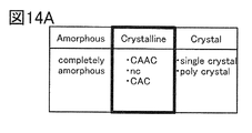
- FIG. 14A is a diagram illustrating classification of crystal structures of IGZO.
- FIG. 14B is a diagram illustrating an XRD spectrum of quartz glass.
- FIG. 14C is a diagram illustrating an XRD spectrum of crystalline IGZO.
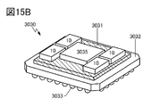
- 15A and 15B are diagrams illustrating an example of an electronic component.
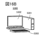
- 16A, 16B, 16C, 16D, 16E, and 16F are diagrams illustrating examples of electronic devices.
- 17A and 17B are diagrams illustrating examples of electronic devices.
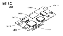
- 18A, 18B, and 18C are diagrams illustrating examples of electronic devices.
- FIG. 19 is a diagram showing various storage devices layer by layer.
- 20A and 20B are diagrams illustrating examples of electronic devices.
- film and the term “layer” can be interchanged with each other.
- conductive layer to the term “conductive film”.
- insulating film to the term “insulating layer”.
- gate electrode on the gate insulating layer does not exclude one including another component between the gate insulating layer and the gate electrode.
- the term “electrically connected” includes the case where they are connected via “an object having some electrical action”.
- the “object having some kind of electrical action” is not particularly limited as long as it can transfer an electric signal between the connection targets.
- things having some kind of electrical action include electrodes and wirings, switching elements such as transistors, resistance elements, inductors, capacitance elements, and other elements having various functions.
- switching elements such as transistors, resistance elements, inductors, capacitance elements, and other elements having various functions.
- electrode and “wiring” do not functionally limit these components.
- electrode may be used as part of “wiring” and vice versa.
- a “terminal” in an electric circuit refers to a portion where input or output of current or potential and reception (or transmission) of a signal are performed. Therefore, part of the wiring or the electrode may function as a terminal.
- the “capacitance” has a structure in which two electrodes face each other via an insulator (dielectric).
- the term “capacitance element” includes the above-mentioned “capacitance”. That is, in this specification and the like, the term “capacitance element” means that two electrodes face each other through an insulator, that two wirings face each other through an insulator, or The case where two wires are arranged via an insulator is included.
- the term “voltage” often refers to a potential difference between a certain potential and a reference potential (eg, a ground potential). Therefore, the voltage and the potential difference can be rephrased.
- a transistor is an element having at least three terminals including a gate, a drain, and a source.
- a channel formation region is provided between the drain (drain terminal, drain region, or drain electrode) and the source (source terminal, source region, or source electrode), and the source and drain are connected via the channel formation region. An electric current can be passed between them.
- a channel formation region refers to a region in which a current mainly flows.
- the functions of the source and the drain may be switched when a transistor of different polarity is used or when the direction of current changes in circuit operation. Therefore, in this specification and the like, the terms source and drain can be interchanged.
- off-state current refers to drain current when a transistor is in an off state (also referred to as a non-conducting state or a blocking state).
- the off-state is a state in which the gate voltage Vgs with respect to the source is lower than the threshold voltage Vth in the n-channel transistor, and the gate voltage Vgs with respect to the source in the p-channel transistor. It is a state higher than the threshold voltage Vth. That is, the off-state current of the n-channel transistor may be a drain current when the gate voltage Vgs with respect to the source is lower than the threshold voltage Vth.
- off-state current may refer to the source current when the transistor is off. Further, it may be referred to as a leak current in the same meaning as an off current. In this specification and the like, off-state current may refer to current flowing between a source and a drain when a transistor is in an off state.
- the on-state current may refer to a current flowing between a source and a drain when the transistor is in an on state (also referred to as a conductive state).
- a metal oxide is a metal oxide in a broad sense. Metal oxides are classified into oxide insulators, oxide conductors (including transparent oxide conductors), oxide semiconductors, and the like.
- the metal oxide when a metal oxide is used for a channel formation region of a transistor, the metal oxide may be referred to as an oxide semiconductor. That is, when the metal oxide has at least one of an amplifying action, a rectifying action, and a switching action, the metal oxide can be called a metal oxide semiconductor. That is, a transistor including a metal oxide in a channel formation region can be referred to as an “oxide semiconductor transistor” or an “OS transistor”.
- a metal oxide having nitrogen may be referred to as a metal oxide.
- the metal oxide containing nitrogen may be referred to as a metal oxynitride. Details of the metal oxide will be described later.
- a memory device is a memory device that can function by utilizing semiconductor characteristics and is also called a memory.
- the memory device has a structure in which a plurality of layers including OS transistors is stacked over a layer including transistors formed over a semiconductor substrate.
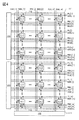
- FIG. 1 is a perspective view showing a configuration example of a storage device 10 according to one embodiment of the present invention.
- the memory device 10 includes a layer 100 and layers 200_1 to 200_1 (l is an integer of 1 or more).
- layers 200_1 to 200_1 l is an integer of 1 or more.
- reference numerals such as "_1" and [_2] are used to distinguish a plurality of elements having similar functions. That is, when referring to an arbitrary layer among the layers 200_1 to 200_1, the reference numeral of the layer 200 is used for description, and when it is necessary to specify one, reference numerals such as the layer 200_1 and the layer 200_2 are used. explain.
- the memory device 10 includes a layer 200_1 stacked over the layer 100, a layer 200_2 stacked over the layer 200_1, and the layers 200_3 (not shown) to
- the layer 200_1 also has a structure in which layers are stacked in order. Further, in order to make the explanation easy to understand, the case where l is 2 will be described hereinafter in the present embodiment.
- FIG. 2 is a schematic perspective view showing a configuration example of the storage device 10 according to one embodiment of the present invention.
- the memory device 10 illustrated in FIG. 2 includes a layer 100, a layer 200_1, and a layer 200_2, the layer 200_1 is stacked over the layer 100, and the layer 200_2 is stacked over the layer 200_1. ing.
- Each of the layer 100, the layer 200_1, and the layer 200_2 is provided with a circuit which can function by utilizing semiconductor characteristics.
- the layer 100 includes the peripheral circuit 101 and the layer 200_1 and the layer 200_1.
- a memory cell array 111 is provided in 200_2. Note that in the drawings described in this specification and the like, main signal flows are indicated by arrows or lines, and power supply lines and the like may be omitted.
- the peripheral circuit 101 has a row decoder 121, a word line driver circuit 122, a word line driver circuit 123, a column decoder 131, a bit line driver circuit 132, a page buffer 138, an output circuit 141, and a control logic circuit 151.
- the peripheral circuit 101 has a function as a drive circuit and a control circuit of the memory cell array 111.
- the peripheral circuit 101 is configured using transistors formed on the semiconductor substrate SUB.
- the semiconductor substrate SUB is not particularly limited as long as it can form the channel region of the transistor.
- a single crystal silicon substrate, a single crystal germanium substrate, a compound semiconductor substrate (SiC substrate, GaN substrate, etc.), an SOI (Silicon on Insulator) substrate, etc. can be used.
- the SOI substrate is formed by implanting oxygen ions into a mirror-polished wafer and then heating it at a high temperature to form an oxide layer at a certain depth from the surface and eliminate defects generated in the surface layer.
- An SOI substrate formed by the above may be used.
- a transistor formed using a single crystal substrate has a single crystal semiconductor in a channel formation region.
- a single crystal silicon substrate is used for the semiconductor substrate SUB.
- a transistor formed over a single crystal silicon substrate is called a Si transistor.
- the peripheral circuit 101 configured by using Si transistors can operate at high speed.
- the memory cell array 111 has a plurality of memory cells 112, and the memory cells 112 are configured using OS transistors. Since the OS transistor is a thin film transistor, the memory cell array 111 can be stacked over the semiconductor substrate SUB.
- the OS transistor since the band gap of the oxide semiconductor is 2.5 eV or more, preferably 3.0 eV or more, the OS transistor has a small leak current due to thermal excitation and an extremely small off current.
- the metal oxide used for the channel formation region of the OS transistor is preferably an oxide semiconductor containing at least one of indium (In) and zinc (Zn).
- a typical example of such an oxide semiconductor is an In-M-Zn oxide (the element M is Al, Ga, Y, or Sn).
- the oxide semiconductor can be i-type (intrinsic) or substantially i-type.
- Such an oxide semiconductor can be referred to as a highly purified oxide semiconductor. Note that details of the OS transistor will be described in Embodiment 3.
- the memory cell 112 has a function of storing data by accumulating and holding charges.
- the memory cell 112 may have a function of storing binary (high level or low level) data, or may have a function of storing four or more levels of data. Alternatively, it may have a function of storing analog data.
- the OS transistor Since the off-state current of the OS transistor is extremely small, the OS transistor is suitable as a transistor used for the memory cell 112.
- the OS transistor can have an off-state current per channel width of 1 ⁇ m of 100 zA/ ⁇ m or less, 10 zA/ ⁇ m or less, 1 zA/ ⁇ m or less, or 10 yA/ ⁇ m or less, for example.
- the OS transistor Since the OS transistor has a feature that the off-state current does not easily increase even at high temperature, the memory device 10 can operate even when the temperature of the environment where it is installed is high. In addition, the data stored in the memory cell 112 is less likely to be lost even under high temperature due to heat generation of the peripheral circuit 101. By using the OS transistor, the reliability of the memory device 10 can be improved.
- a transistor other than the OS transistor may be used as long as the off-state current is low.
- a transistor including a semiconductor with a wide bandgap in a channel formation region may be used.
- the semiconductor with a large band gap may refer to a semiconductor with a band gap of 2.2 eV or more, and examples thereof include silicon carbide, gallium nitride, and diamond.
- memory cells 112 are arranged in a matrix (also referred to as a matrix), and each memory cell 112 is electrically connected to a wiring WL and a wiring BL.
- the memory cell 112 is selected by the potential applied to the wiring WL, and data is written to the selected memory cell 112 through the wiring BL.
- the memory cell 112 is selected by the potential applied to the wiring WL and data is read from the selected memory cell 112 through the wiring BL. That is, the wiring WL functions as a word line of the memory cell 112 and the wiring BL functions as a bit line of the memory cell 112.
- the wiring WL and the wiring BL illustrated in FIG. 2 each include a plurality of wirings.
- the wiring WL includes a plate line PL, a write word line WWL, a read word line RWL, a wiring BG1, and a wiring BG2, and the wiring BL includes a read bit line RBL and a write bit line WBL. (See Figures 3 and 4).
- the memory cell array 111 provided in the layer 200_1 is electrically connected to the word line driver circuit 122 through the wiring WL, and the memory cell array 111 provided in the layer 200_2 is connected through the wiring WL in the word line driver circuit. It is electrically connected to 123.
- the memory cell array 111 provided in the layer 200_1 and the memory cell array 111 provided in the layer 200_2 are electrically connected to the bit line driver circuit 132 through the wiring BL.
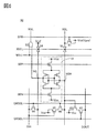
- FIG. 3 is a block diagram showing a configuration example of the storage device 10.
- the memory cell array 111 provided in the layer 200_2 and the word line driver circuit 123 are omitted, and only one memory cell 112 included in the memory cell array 111 is illustrated as a representative.
- the memory device 10 has a peripheral circuit 101 and a memory cell array 111.
- the peripheral circuit 101 has a row decoder 121, a word line driver circuit 122, a column decoder 131, a bit line driver circuit 132, a page buffer 138, an output circuit 141, and a control logic circuit 151.
- the memory cell array 111 includes a plurality of memory cells 112 (only one is shown in FIG. 3), and the memory cell 112 includes a plate line PL, a write word line WWL, a read word line RWL, a wiring BG1, and a wiring BG2.
- the bit line driver circuit 122 is electrically connected to the bit line driver circuit 122 via the read bit line RBL and the write bit line WBL.
- the potential Vss, the potential Vdd, the potential Vdh, the precharge potential Vpre, and the reference potential Vref are input to the memory device 10.
- the potential Vdh is the high power supply potential of the write word line WWL.
- a clock signal CLK, a chip enable signal CE, a global write enable signal GW, a byte write enable signal BW, an address signal ADDR, and a data signal WDATA are input to the memory device 10, and the memory device 10 outputs a data signal RDATA.
- these signals are digital signals represented by a high level or a low level (sometimes represented by High or Low, H or L, 1 or 0, etc.).
- a high level of a digital signal is represented by the potential Vdd and a low level thereof is represented by the potential Vss.
- the potential Vdh is used for the high level and the potential Vss is used for the low level of the write word line WWL.
- the byte write enable signal BW, the address signal ADDR, the data signal WDATA, and the data signal RDATA are signals having a plurality of bits.
- the byte write enable signal has BW[0] to BW[3], and when it is necessary to specify one bit, it is referred to as, for example, the byte write enable signal BW[0].
- the byte write enable signal BW[0] indicates an arbitrary bit.
- the byte write enable signal BW can be 4 bits, and the data signal WDATA and the data signal RDATA can be 32 bits. That is, the byte write enable signal BW, the data signal WDATA, and the data signal RDATA are the byte write enable signal BW[3:0], the data signal WDATA[31:0], and the data signal RDATA[31:0], respectively. It is written.
- the above-described circuits, signals, and potentials can be appropriately discarded as necessary.
- another circuit, another signal, or another potential may be added.
- the control logic circuit 151 processes the chip enable signal CE and the global write enable signal GW to generate control signals for the row decoder 121 and the column decoder 131. For example, when the chip enable signal CE is high level and the global write enable signal GW is low level, the row decoder 121 and the column decoder 131 perform a read operation, the chip enable signal CE is high level, and the global write enable signal GW is high level. In this case, the row decoder 121 and the column decoder 131 perform the write operation, and when the chip enable signal CE is at the low level, the row decoder 121 and the column decoder 131 are in the standby state regardless of the high level and the low level of the global write enable signal GW. It can be an action.
- the signal processed by the control logic circuit 151 is not limited to this, and another signal may be input as necessary.
- control logic circuit 151 processes the byte write enable signal BW[3:0] to control the write operation. Specifically, when the byte write enable signal BW[0] is at high level, the row decoder 121 and the column decoder 131 perform the write operation of the data signal WDATA[7:0]. Similarly, when the byte write enable signal BW[1] is at the high level, the write operation of the data signal WDATA[15:8] is performed. When the byte write enable signal BW[2] is at the high level, the data signal WDATA[23:16]. ], and when the byte write enable signal BW[3] is at a high level, the data signal WDATA[31:24] is written.
- the address signal ADDR is input to the row decoder 121 and the column decoder 131, in addition to the above-described control signal generated by the control logic circuit 151.
- the row decoder 121 decodes the address signal ADDR and generates a control signal for the word line driver circuit 122.
- the word line driver circuit 122 has a function of driving the plate line PL, the write word line WWL, the read word line RWL, the wiring BG1, and the wiring BG2, or a function of applying a predetermined potential.
- the word line driver circuit 122 selects the write word line WWL or the read word line RWL of the access target row based on the control signal of the row decoder 121.
- the word line driver circuit 122 may have a function of selecting the wiring BG1 or the wiring BG2.
- the predecoder 124 may be provided.
- the predecoder 124 has a function of decoding the address signal ADDR and determining a block to be accessed.
- the column decoder 131, the bit line driver circuit 132, and the page buffer 138 have a function of writing data input by the data signal WDATA into the memory cell array 111, a function of reading data from the memory cell array 111, and amplification and output of read data. It has a function of outputting to the circuit 141 and the like.
- the output circuit 141 outputs the data read from the memory cell array 111 by the column decoder 131 and the bit line driver circuit 132 and stored in the page buffer 138 as a data signal RDATA.
- the bit line driver circuit 132 has a precharge circuit 133, a sense amplifier circuit 134, an output MUX (multiplexer) circuit 135, and a write driver circuit 136.
- the precharge circuit 133, the sense amplifier circuit 134, the output MUX circuit 135, and the write driver circuit 136 will be described later.
- FIG. 4 is a block diagram showing a configuration example of the memory cell array 111.
- FIG. 4 shows two memory cell arrays 111, a word line driver circuit 122, a word line driver circuit 123, and a bit line driver circuit 132.
- the memory cell array 111 is a plate line PL and a write word line.
- the state where the memory cell array 111 is electrically connected to the bit line driver circuit 132 via the read bit line RBL and the write bit line WBL.
- the memory cell array 111 electrically connected to the word line driver circuit 122 through the wiring WL is the memory cell array 111 provided in the layer 200_1 and electrically connected to the word line driver circuit 123 through the wiring WL.
- the memory cell array 111 connected to is the memory cell array 111 provided in the layer 200_2.
- One memory cell array 111 has m (m is an integer of 1 or more) in one column, n (n is an integer of 1 or more) in one row, and a total of m ⁇ n memory cells 112. They are arranged in a matrix. Although the same memory cell array 111 is provided in the layer 200_1 and the layer 200_2 in FIG. 4, the memory cell array 111 provided in the layer 200_1 and the memory cell array 111 provided in the layer 200_2 have memory cells. The number of 112 and the like may be different.
- the address of the memory cell 112 is also shown, and [1,1], [i,1], [m,1], [1,j], [i,j], [m,j]. , [1, n], [i, n], [m, n] (i is an integer of 1 or more and m or less, j is an integer of 1 or more and n or less) are addresses of the memory cell 112.
- the memory cell 112 described as [i,j] is the memory cell 112 arranged in the i-th row and the j-th column.
- the memory cell 112 arranged in the i-th row and the j-th column has a plate line PL[i], a write word line WWL[i], a read word line RWL[i], a wiring BG1[i], a wiring BG2[i], a read bit.
- the line RBL[j] and the write bit line WBL[j] are electrically connected.
- the memory cells 112 arranged in the i-th row and the j-th column include the plate line PL[i], the write word line WWL[i], the read word line RWL[i], the wiring BG1[i], and the wiring BG2[i. ]
- the memory device 10 includes 2 ⁇ m plate lines PL, 2 ⁇ m write word lines WWL, 2 ⁇ m read word lines RWL, 2 ⁇ m wirings BG1, and 2 ⁇ m wirings. It has BG2, n read bit lines RBL, and n write bit lines WBL.
- FIG. 5A is a circuit diagram showing a configuration example of the memory cell 112.
- the memory cell 112 has a transistor 11, a transistor 12, and a capacitor C11.
- the transistor 11 may be referred to as a writing transistor and the transistor 12 may be referred to as a reading transistor.
- the transistors 11 and 12 each have a front gate (sometimes referred to simply as a gate) and a back gate.
- One of the source and the drain of the transistor 11 is electrically connected to the write bit line WBL, and the other of the source and the drain of the transistor 11 is electrically connected to the front gate of the transistor 12 and one terminal of the capacitor C11.
- the front gate of the transistor 11 is electrically connected to the write word line WWL, and the back gate of the transistor 11 is electrically connected to the wiring BG1.
- One of the source and the drain of the transistor 12 is electrically connected to the read bit line RBL, the other of the source and the drain of the transistor 12 is electrically connected to the read word line RWL, and the back gate of the transistor 12 is the wiring BG2. Electrically connected to.
- the other terminal of the capacitive element C11 is electrically connected to the plate line PL.
- the wiring BG1 functions as a wiring for applying a predetermined potential to the back gate of the transistor 11
- the wiring BG2 functions as a wiring for applying a predetermined potential to the back gate of the transistor 12.
- the plate line PL functions as a wiring for applying a predetermined potential to the other terminal of the capacitive element C11.
- a connection portion in which the other of the source and the drain of the transistor 11, the front gate of the transistor 12, and one terminal of the capacitor C11 are electrically connected is referred to as a node N11.
- the transistor 11 has a function as a switch for electrically connecting or disconnecting the node N11 and the write bit line WBL.
- the memory cell 112 may have a configuration that does not have the capacitive element C11.
- Data writing is performed by applying a high-level potential to the write word line WWL to make the transistor 11 conductive and electrically connecting the node N11 and the write bit line WBL. Specifically, when the transistor 11 is conductive, a potential corresponding to the data to be written is applied to the write bit line WBL and the potential is written to the node N11. After that, a low-level potential is applied to the write word line WWL and the transistor 11 is turned off, so that the potential of the node N11 is held.
- a predetermined potential is applied to the read bit line RBL, then the read bit line RBL is electrically floated, and a low-level potential is applied to the read word line RWL. Done.
- applying a predetermined potential to the read bit line RBL and then bringing the read bit line RBL into a floating state is referred to as precharging the read bit line RBL.
- the transistor 12 has a potential difference between the source and the drain, and the current flowing between the source and the drain of the transistor 12 is held in the node N11. It depends on the potential. Therefore, the potential held in the node N11 can be read by reading the potential change of the read bit line RBL when the read bit line RBL is in a floating state.
- the row in which the memory cell 112 for writing data is arranged is selected by the write word line WWL for applying a high-level potential, and the row in which the memory cell 112 for reading data is arranged has a low-level potential. It is selected by the read word line RWL to be applied. On the contrary, the row in which the memory cell 112 in which data is not written is arranged applies the low level potential to the write word line WWL, and the row in which the memory cell 112 in which data is not read is arranged is the read word line RWL. By applying the same potential as the precharge potential to the read bit line RBL, it can be made unselected.
- the memory cell 112 can store data by accumulating and retaining charges in the node N11.
- the node N11 can store binary data.
- the memory cell 112 is a gain cell type memory cell including two-transistor one-capacitance element (or two-transistor).
- the gain cell type memory cell can operate as a memory by amplifying the accumulated charge with the nearest transistor even if the charge accumulation capacity is small.
- the memory cell 112 is the NOSRAM described above.
- the transistors 11 and 12 are transistors (OS transistors) each including a metal oxide in a channel formation region.
- OS transistors transistors
- the transistors 11 and 12 indium, an element M (the element M is aluminum, gallium, yttrium, copper, vanadium, beryllium, boron, titanium, iron, nickel, germanium, zirconium, molybdenum, lanthanum,
- a metal oxide having any one of cerium, neodymium, hafnium, tantalum, tungsten, magnesium, or the like) and zinc can be used.
- a metal oxide composed of indium, gallium and zinc is preferable.
- the off-state current of the OS transistor is extremely small, the potential written in the node N11 can be held for a long time by using the OS transistor as the transistor 11. That is, the data written in the memory cell 112 can be retained for a long time.
- the capacitance of the capacitor C11 can be reduced.
- the capacitive element C11 the gate capacitance of a transistor, the parasitic capacitance of wiring, or the like can be used. Therefore, in the memory cell 112, it is not necessary to form a capacitor element separately from a transistor or a wiring, and the memory cell 112 may have a structure without the capacitor element C11. With the structure in which the memory cell 112 does not include the capacitor C11, the area of the memory cell 112 can be reduced.
- the memory cell array 111 can be stacked over the peripheral circuit 101 by using OS transistors for the transistors 11 and 12.
- the threshold voltage of the transistors 11 and 12 is increased or decreased. can do.
- the threshold voltage shifts to a negative value, and the potential applied to the back gates of the transistors 11 and 12 is lowered.
- the threshold voltage shifts to the plus.
- the on-state current of the transistor can be increased and the memory cell 112 can operate at high speed.
- shifting the threshold voltage to plus off-state current of the transistor can be reduced and the memory cell 112 can hold data for a long time.
- the back gate of the transistor 11 is electrically connected to the wiring BG1 and the back gate of the transistor 12 is electrically connected to the wiring BG2, the potential applied to the wiring BG1 is lowered.
- the off-state current of the transistor 11 can be reduced, and the on-state current of the transistor 12 can be increased by increasing the potential applied to the wiring BG2.
- the transistor 11 and the transistor 12 can be transistors for each purpose.
- the wiring BG1 and the wiring BG2 may be integrated into one wiring, and the same potential may be applied to the back gate of the transistor 11 and the back gate of the transistor 12.
- the wiring BG2 may be driven using the word line driver circuit 122 or the word line driver circuit 123.
- the word line driver circuit 122 or the word line driver circuit 123 can increase the on-state current of the transistor 12 in the reading operation by increasing the potential applied to the wiring BG2 in the row to be read. On the contrary, by applying a low potential to the wiring BG2 other than the row to be read, the off-state current of the transistor 12 which is not performing the reading operation can be reduced.
- the read operation of the memory cell 112 is increased and the off-state current of the transistor 12 included in the other memory cells 112 is reduced. By doing so, the current leaking to the read bit line RBL can be reduced. The accuracy of the read operation can be improved by reducing the current leaking to the read bit line RBL.
- FIG. 5B is a circuit diagram showing a configuration example of the memory cell 113.
- the memory cell 113 has a transistor 11, a transistor 12, and a capacitor C11.
- One of the source and the drain of the transistor 11 is electrically connected to the write bit line WBL, and the other of the source and the drain of the transistor 11 is the other of the front gate of the transistor 12, the back gate of the transistor 12, and one of the capacitor C11. , And the front gate of the transistor 11 is electrically connected to the write word line WWL and the back gate of the transistor 11.
- One of the source and the drain of the transistor 12 is electrically connected to the read bit line RBL, and the other of the source and the drain of the transistor 12 is electrically connected to the read word line RWL.
- the other terminal of the capacitive element C11 is electrically connected to the plate line PL.
- the on-state current of the transistor 11 can be increased.
- the on-state current of the transistor 12 can be increased. That is, the memory cell 113 can operate at high speed.
- each of the transistor 11 and the transistor 12 may be a transistor having no back gate.
- the manufacturing process of the transistor can be simplified.
- FIG. 6 is a circuit diagram showing a configuration example of the circuit 50.
- the circuit 50 includes transistors 61 to 66, a sense amplifier circuit 51, an AND circuit 52, an analog switch 53, and an analog switch 54.
- the circuit 50 operates according to the signal SEN, the signal SEP, the signal BPR, the signal RSEL[3:0], the signal WSEL, the signal GRSEL[3:0], and the signal GWSEL[15:0]. It should be noted that one of the 4-bit signals RSEL[3:0] is input to one circuit 50. The same applies to other signals having a plurality of bits (GRSEL[3:0] etc.).
- the data DIN[31:0] is written to the memory cell array 111 and the data DOUT[31:0] is read from the memory cell array 111 by the bit line driver circuit 132.
- One circuit 50 writes any 1-bit data of the 32-bit data DIN [31:0] to the memory cell array 111, and writes any 1-bit data of the 32-bit data DOUT [31:0]. It has a function of reading data from the memory cell array 111.
- the data DIN[31:0] and the data DOUT[31:0] are internal signals, and the data DIN[31:0] are signals supplied from the page buffer 138 to the bit line driver circuit 132.
- DOUT[31:0] is a signal output from the bit line driver circuit 132 to the page buffer 138.
- a data signal WDATA is input to the page buffer 138 from the outside of the storage device 10, and the page buffer 138 outputs the data signal RDATA to the outside of the storage device 10 via the output circuit 141.
- the page buffer 138 can store at least a data amount (n bits) that can be stored in one row in the memory cell array 111. In this embodiment, it is preferable that data of 128 bits or more can be stored.
- the transistor 61 constitutes the precharge circuit 133.
- the read bit line RBL is precharged to the precharge potential Vpre by the transistor 61. Note that in this embodiment, the case where the potential Vdd (high level) is used as the precharge potential Vpre is described (in FIG. 6 and FIG. 7, written as Vdd (Vpre)).
- the signal BPR is a precharge signal, and the conduction state of the transistor 61 is controlled by the signal BPR.
- the sense amplifier circuit 51 constitutes a sense amplifier circuit 134.
- the sense amplifier circuit 51 determines the high level or the low level of the data input to the read bit line RBL during the read operation.
- the sense amplifier circuit 51 also functions as a latch circuit that temporarily holds the data DIN input from the write driver circuit 136 during the write operation.
- the sense amplifier circuit 51 shown in FIG. 6 is a latch type sense amplifier.
- the sense amplifier circuit 51 has two inverter circuits, and the input node of one inverter circuit is connected to the output node of the other inverter circuit.
- the input node of one of the inverter circuits is node NS and the output node is node NSB, complementary data is held at nodes NS and NSB.
- the signal SEN and the signal SEP are sense amplifier enable signals for activating the sense amplifier circuit 51, and the reference potential Vref is a read determination potential.
- the sense amplifier circuit 51 determines, with reference to the reference potential Vref, whether the potential of the node NSB at the time of activation is high level or low level.
- the AND circuit 52 controls the conduction state between the node NS and the write bit line WBL.
- the analog switch 53 controls the conduction state between the node NSB and the read bit line RBL, and the analog switch 54 controls the conduction state between the node NS and the wiring that supplies the reference potential Vref.
- the potential of the read bit line RBL is transmitted to the node NSB by the analog switch 53, and when the potential of the read bit line RBL becomes lower than the reference potential Vref, the sense amplifier circuit 51 determines that the read bit line RBL is at the low level. To do. When the potential of the read bit line RBL does not become lower than the reference potential Vref, the sense amplifier circuit 51 determines that the read bit line RBL is at high level.
- the signal WSEL is a write selection signal and controls the AND circuit 52.
- the signals RSEL[3:0] are read selection signals and control the analog switch 53 and the analog switch 54.
- the transistor 62 and the transistor 63 form an output MUX circuit 135.
- the signals GRSEL[3:0] are global read selection signals and control the output MUX circuit 135.
- the output MUX circuit 135 has a function of selecting 32 read bit lines RBL from which data is read out of 128 read bit lines RBL.
- the output MUX circuit 135 functions as a multiplexer with 128 inputs and 32 outputs.
- the output MUX circuit 135 reads the data DOUT[31:0] from the sense amplifier circuit 134 and outputs it to the page buffer 138.
- the transistors 64 to 66 form a write driver circuit 136.
- the signals GWSEL[15:0] are global write selection signals and control the write driver circuit 136.
- the write driver circuit 136 has a function of writing the data DIN[31:0] to the sense amplifier circuit 134.
- the write driver circuit 136 has a function of selecting a column to which the data DIN[31:0] is written.
- the write driver circuit 136 writes data in byte units, half word units, or 1 word units according to the signal GWSEL [15:0].
- the circuit 50 is electrically connected to the data DIN[h] (h is an integer of 0 or more and 31 or less) every four columns.
- the circuit 50 is electrically connected to the data DOUT[h] every four columns.
- FIG. 7 is a timing chart illustrating an operation example of the memory cell 112.
- the potential relationship between the write word line WWL, the read word line RWL, the read bit line RBL, and the write bit line WBL in the write operation and the read operation of the memory cell 112 will be described. Further, a case where the wiring BG2 is driven using the word line driver circuit 122 or the word line driver circuit 123 will be described later.
- a period Twrite is a period in which a writing operation is performed and a period Tread is a period in which a reading operation is performed.
- the high level of the read word line RWL, the read bit line RBL, and the write bit line WBL is the potential Vdd, and the low level thereof is the potential Vss.
- the high level of the write word line WWL is the potential Vdh, and the low level of the write word line WWL is the potential Vss.
- the potential Vdd is applied to the read word line RWL and the read bit line RBL.
- the read bit line RBL is precharged with the potential Vdd.
- the potential Vss is applied to the read word line RWL of the row in which the memory cell 112 for reading data is arranged while the read bit line RBL is in the floating state, when the data written in the node N11 is high level, the transistor 12 becomes conductive, and the potential of the read bit line RBL starts to drop.
- the sense amplifier circuit 51 determines that the read bit line RBL is at the low level.
- the sense amplifier circuit 51 determines that the read bit line RBL is at high level.
- the potential Vss is applied to the write bit line WBL and the write word line WWL.
- the high level of the wiring BG2 can be set to the potential Vdh and the low level of the wiring BG2 can be set to the potential Vss.
- the potential Vss is applied to the wiring BG2
- the potential Vdh is applied to the wiring BG2 in the row where the memory cell 112 from which data is read is arranged.
- the on-state current of the transistor 12 included in the memory cell 112 from which data is read can be increased. Further, the potential Vss is applied to the wiring BG2, so that the off-state current of the transistor 12 can be reduced.
- the memory device 10 has a gain cell type memory cell composed of n-channel type transistors, and the write word line WWL, the read word line RWL, the write bit line WBL, and the read bit line RBL are A high level or a low level is represented by three types of potentials (potential Vss, potential Vdd, and potential Vdh). That is, the storage device 10 can be operated with a small number of power sources, and the cost of an electronic device equipped with the storage device 10 can be reduced.
- the gain cell type memory cell requires at least two transistors per memory cell, and it was difficult to increase the number of memory cells that can be arranged per unit area.
- OS transistors are used as the transistors forming the memory cell 112.
- a plurality of memory cell arrays 111 can be stacked and provided on the semiconductor substrate SUB on which the peripheral circuit 101 is formed. That is, the amount of data that can be stored per unit area can be increased.
- the gain cell type memory cell can operate as a memory by amplifying the accumulated charge with the nearest transistor even when the charge accumulation capacity is small. Furthermore, the capacity of the capacitor C11 can be reduced by using an OS transistor whose off-state current is extremely low as a transistor included in the memory cell 112. Alternatively, a gate capacitance of a transistor, a parasitic capacitance of a wiring, or the like can be used as the capacitor C11, and the capacitor C11 can be omitted. That is, the area of the memory cell 112 can be reduced.
- FIG. 8A and 8B illustrate a structure of the memory cell 860 included in the memory device according to one embodiment of the present invention.
- FIG. 8A is a top view of the periphery of the memory cell 860.
- 8B is a cross-sectional view of the memory cell 860, and FIG. 8B corresponds to a portion indicated by a dashed-dotted line A1-A2 in FIG. 8A.
- 8B shows a cross section in the channel length direction of the transistor 600 and a cross section in the channel width direction of the transistor 700.
- the X direction, the Y direction, and the Z direction shown in FIG. 8A are directions orthogonal to or intersecting with each other.
- the X direction and the Y direction are parallel or substantially parallel to the substrate surface
- the Z direction is perpendicular or substantially vertical to the substrate surface.
- the memory cell 860 described in this embodiment includes a transistor 600, a transistor 700, and a capacitor 655.
- the memory cell 860 corresponds to the memory cell 112 described in the above embodiment, and the transistor 600, the transistor 700, and the capacitor 655 are the transistor 11, the transistor 12, and the capacitor described in the above embodiment, respectively. It corresponds to the element C11. Therefore, one of the source and the drain of the transistor 600, the gate of the transistor 700, and one of the electrodes of the capacitor 655 are electrically connected to each other.
- the transistor 600 and the transistor 700 are provided over the insulator 614, and the insulator 680 is provided over part of the transistor 600 and the transistor 700.
- An insulator 682 is placed over the 600, the transistor 700, and the insulator 680, an insulator 685 is placed over the insulator 682, a capacitor 655 is placed over the insulator 685, and a capacitor 655 is placed over the capacitor 655.
- An insulator 688 is placed.
- the insulator 614, the insulator 680, the insulator 682, the insulator 685, and the insulator 688 function as an interlayer film.
- the transistor 600 includes an insulator 616 over an insulator 614, a conductor 605 (a conductor 605 a, and a conductor 605 b) which is arranged so as to be embedded in the insulator 616, over the insulator 616, and a conductor.
- Insulator 622 over body 605, insulator 624 over insulator 622, oxide 630a over insulator 624, oxide 630b over oxide 630a, oxide 643a over oxide 630b, and oxide.
- the oxide 630c is in contact with the side surface of the oxide 643a, the side surface of the oxide 643b, the side surface of the conductor 642a, and the side surface of the conductor 642b, respectively.
- the top surface of the conductor 660 is arranged to be substantially aligned with the top surface of the insulator 650, the top surface of the oxide 630c, and the top surface of the insulator 680.
- the insulator 682 is in contact with the top surfaces of the conductor 660, the insulator 650, the oxide 630c, and the insulator 680, respectively.
- the oxide 630a, the oxide 630b, and the oxide 630c may be collectively referred to as the oxide 630.
- the oxide 643a and the oxide 643b may be collectively referred to as the oxide 643.
- the conductor 642a and the conductor 642b may be collectively referred to as a conductor 642.
- the conductor 660 functions as a gate, and the conductors 642a and 642b function as a source and a drain, respectively. Further, the conductor 605 functions as a back gate.
- the transistor 600 is formed in a self-aligned manner so that the conductor 660 functioning as a gate fills the opening formed by the insulator 680 or the like. As described above, in the memory device according to this embodiment, the conductor 660 can be reliably arranged in the region between the conductor 642a and the conductor 642b without alignment.
- the transistor 700 includes the insulator 616 over the insulator 614, the conductor 705 (the conductor 705a, and the conductor 705b) arranged so as to be embedded in the insulator 616, the insulator 616, and the conductor 705.
- the oxide 730c, the insulator 750 over the oxide 730c, and the conductor 760 (the conductor 760a and the conductor 760b) which is located over the insulator 750 and overlaps with the oxide 730c.
- the oxide 730c is in contact with the side surface of the oxide 743a, the side surface of the oxide 743b, the side surface of the conductor 742a, and the side surface of the conductor 742b, respectively.
- the top surface of the conductor 760 is arranged to be substantially aligned with the top surface of the insulator 750, the top surface of the oxide 730c, and the top surface of the insulator 680.
- the insulator 682 is in contact with the top surfaces of the conductor 760, the insulator 750, the oxide 730c, and the insulator 680, respectively.
- the oxide 730a, the oxide 730b, and the oxide 730c may be collectively referred to as the oxide 730.
- the oxide 743a and the oxide 743b may be collectively referred to as an oxide 743.
- the conductor 742a and the conductor 742b may be collectively referred to as a conductor 742.
- the conductor 760 functions as a gate, and the conductors 742a and 742b function as a source and a drain, respectively.
- the conductor 705 functions as a back gate.
- the transistor 700 is formed in a self-aligned manner so that the conductor 760 functioning as a gate fills the opening formed by the insulator 680 or the like. As described above, in the memory device according to this embodiment, the conductor 760 can be reliably arranged in the region between the conductor 742a and the conductor 742b without alignment.
- the transistor 700 is formed in the same layer as the transistor 600 and has a similar structure. Therefore, although a cross section in the channel length direction of the transistor 700 is not illustrated, it has a structure similar to that of the transistor 600 in the channel length direction illustrated in FIG. 8B. That is, the oxide 743 and the conductor 742, which are not illustrated in the cross-sectional view, also have the same structure as the oxide 643 and the conductor 642 illustrated in FIG. 8B. Note that although a cross section in the channel width direction of the transistor 600 is not illustrated, it has a structure similar to that of the transistor 700 in the channel width direction illustrated in FIG. 8B.
- the oxide 730 has a structure similar to that of the oxide 630, and the description of the oxide 630 can be referred to.
- the conductor 705 has a structure similar to that of the conductor 605, and the description of the conductor 605 can be referred to.
- the oxide 743 has a structure similar to that of the oxide 643, and the description of the oxide 643 can be referred to.
- the conductor 742 has a structure similar to that of the conductor 642, and the description of the conductor 642 can be referred to.
- the insulator 750 has a structure similar to that of the insulator 650, and the description of the insulator 650 can be referred to.
- the conductor 760 has a structure similar to that of the conductor 660, and the description of the conductor 660 can be referred to. Unless otherwise specified, the description of the structure of the transistor 600 can be referred to for the structure of the transistor 700 as described above.
- a metal oxide functioning as an oxide semiconductor (hereinafter also referred to as an oxide semiconductor) is preferably used for the oxide 630 and the oxide 730 including a channel formation region.
- an energy gap of 2 eV or more, preferably 2.5 eV or more is preferably used.
- an In-M-Zn oxide (the element M is aluminum, gallium, yttrium, tin, copper, vanadium, beryllium, boron, titanium, iron, nickel, germanium, zirconium, molybdenum, lanthanum, cerium).
- the element M is preferably aluminum, gallium, yttrium, or tin.
- an In-M oxide, an In-Zn oxide, or an M-Zn oxide may be used as the oxide semiconductor.
- the transistors 600 and 700 each including an oxide semiconductor in the channel formation region have extremely low leakage current (off-state current) in the non-conduction state, and thus can provide a memory device with low power consumption. Further, the off-state current of the transistors 600 and 700 hardly increases even in a high temperature environment. Specifically, the off-state current hardly increases even at an ambient temperature of room temperature or higher and 200° C. or lower. Therefore, the operation is stable even in a high temperature environment, and a highly reliable storage device can be realized.
- the capacitance value of the capacitor 655 can be set small. As a result, the area occupied by the memory cell 860 can be reduced and the memory device can be integrated.
- the conductor 742a, the conductor 660, the conductor 605, and the conductor 705 preferably extend in the Y direction.
- the conductor 742a functions as the read word line RWL described in the above embodiment.
- the conductor 660 functions as the write word line WWL described in the above embodiment.
- the conductor 605 functions as the wiring BG1 described in the above embodiment.
- the conductor 705 functions as the wiring BG2 described in the above embodiment.
- the capacitor 655 includes a conductor 646a over the insulator 685, an insulator 686 that covers the conductor 646a, and a conductor 656 that is provided over the insulator 686 so as to overlap with at least part of the conductor 646a.
- the conductor 646 a functions as one electrode of the capacitor 655 and the conductor 656 functions as the other electrode of the capacitor 655.
- the insulator 686 functions as a dielectric of the capacitor 655.
- the conductor 656 extend in the Y direction and function as the plate line PL described in any of the above embodiments.
- openings are formed in the insulator 672, the insulator 673, the insulator 680, the insulator 682, and the insulator 685, and the conductor 640 serving as a plug (the conductor 640a, the conductor 640b, the conductor 640c, And a conductor 640d) is provided to be embedded in the opening. Further, the conductor 640 is provided so as to be exposed on the upper surface of the insulator 685.
- the conductor 640a has a lower surface in contact with the conductor 642a and an upper surface in contact with the conductor 646a.
- the lower surface of the conductor 640c is in contact with the conductor 760 and the upper surface is in contact with the conductor 646a. In this manner, one of the source and the drain of the transistor 600, the gate of the transistor 700, and one of the electrodes of the capacitor 655 are electrically connected.
- the lower surface of the conductor 640b is provided in contact with the conductor 642b. Further, a conductor 646b is provided in contact with the top surface of the conductor 640b.
- the conductor 646b is formed in the same layer as the conductor 646a and has a similar structure. As shown in FIG. 8A, the conductor 646b preferably extends in the X direction. With such a structure, the conductor 646b functions as the write bit line WBL described in the above embodiment.
- the lower surface of the conductor 640d is provided in contact with the conductor 742b. Further, a conductor 746 is provided in contact with the top surface of the conductor 640d.
- the conductor 746 is formed in the same layer as the conductor 646a and has a similar structure. As shown in FIG. 8A, the conductor 746 preferably extends in the X direction. With such a structure, the conductor 746 functions as the read bit line RBL described in any of the above embodiments.
- the transistor 600 and the transistor 700 can be formed in the same step; therefore, the manufacturing process of the memory device can be shortened and productivity can be improved. Can be made.
- the transistor 600, the transistor 700, and the capacitor 655 are provided so that the channel length direction of the transistor 600 and the channel width direction of the transistor 700 are parallel to each other. Is not limited to this.
- a memory cell 860 illustrated in FIG. 8 and the like is an example of a structure of a memory device, and a transistor, a capacitor, or the like having an appropriate structure may be arranged as appropriate depending on a circuit structure or a driving method.
- the oxide 630 is provided over the oxide 630a over the insulator 624, the oxide 630b over the oxide 630a, and the oxide 630b, and at least part of the oxide 630 is over the oxide 630b.
- the oxide 630c in contact therewith is preferable.
- the side surface of the oxide 630c is preferably provided in contact with the oxide 643a, the oxide 643b, the conductor 642a, the conductor 642b, the insulator 672, the insulator 673, and the insulator 680.
- oxide 630a By having the oxide 630a below the oxide 630b, diffusion of impurities from the structure formed below the oxide 630a into the oxide 630b can be suppressed. In addition, by having the oxide 630c over the oxide 630b, diffusion of impurities into the oxide 630b from a structure formed above the oxide 630c can be suppressed.
- the transistor 600 has a structure in which three layers of the oxide 630a, the oxide 630b, and the oxide 630c are stacked in the channel formation region and the vicinity thereof, the present invention is not limited to this. ..
- a single layer of the oxide 630b, a two-layer structure of the oxide 630b and the oxide 630a, a two-layer structure of the oxide 630b and the oxide 630c, or a stacked structure of four or more layers may be provided.
- the oxide 630c may have a two-layer structure and a four-layer stacked structure may be provided.
- the oxide 630 preferably has a stacked structure of a plurality of oxide layers in which the atomic ratio of each metal atom is different.
- the atomic ratio of the element M in the constituent elements is higher than the atomic ratio of the element M in the constituent elements in the metal oxide used for the oxide 630b. It is preferable.
- the atomic ratio of the element M to In is preferably higher than the atomic ratio of the element M to In in the metal oxide used for the oxide 630b.
- the atomic ratio of In to the element M is preferably higher than the atomic ratio of In to the element M in the metal oxide used for the oxide 630a.
- a metal oxide that can be used for the oxide 630a or the oxide 630b can be used. Note that in the metal oxide used for the oxide 630c, the atomic ratio of In to the element M may be higher than that in the metal oxide used for the oxide 630b.
- a metal oxide having a composition of [atomic ratio] or its vicinity may be used.
- an In oxide may be used as the oxide 630b.
- a material that can be used for the oxide 630b may be applied to the oxide 630c and the oxide 630c may be provided as a single layer or a stacked layer.
- the oxides 630b and 630c it is preferable to increase the ratio of indium in the film because the on-state current, field-effect mobility, or the like of the transistor can be increased. Further, the above-mentioned composition in the vicinity includes a range of ⁇ 30% of a desired atomic number ratio.
- the oxide 630b may have crystallinity.
- a CAAC-OS c-axis aligned crystalline oxide semiconductor
- An oxide having crystallinity such as CAAC-OS has few impurities and defects (such as oxygen vacancies) and has a high crystallinity and a dense structure. Therefore, extraction of oxygen from the oxide 630b by the source electrode or the drain electrode can be suppressed. Further, even if heat treatment is performed, oxygen can be reduced from being extracted from the oxide 630b, so that the transistor 600 is stable against a high temperature (so-called thermal budget) in a manufacturing process.
- the oxide 630c is preferably provided in the opening provided in the interlayer film including the insulator 680. Therefore, the insulator 650 and the conductor 660 have a region overlapping with the stacked-layer structure of the oxide 630b and the oxide 630a with the oxide 630c interposed therebetween. With such a structure, the oxide 630c and the insulator 650 can be formed by continuous film formation; therefore, the interface between the oxide 630 and the insulator 650 can be kept clean. Therefore, the influence of interface scattering on carrier conduction is reduced, and the transistor 600 can obtain high on-state current and high frequency characteristics.
- An oxide semiconductor having a low carrier concentration is preferably used for the oxide 630 (eg, the oxide 630b).
- the concentration of impurities in the oxide semiconductor may be lowered and the density of defect states may be lowered.
- low impurity concentration and low defect level density are referred to as high-purity intrinsic or substantially high-purity intrinsic.
- impurities in the oxide semiconductor include hydrogen, nitrogen, alkali metals, alkaline earth metals, iron, nickel, silicon, and the like.
- an oxide semiconductor reacts with oxygen which is bonded to a metal atom to be water, which might cause oxygen deficiency (also referred to as V 2 O 3 ) in the oxide semiconductor.
- oxygen deficiency also referred to as V 2 O 3
- a defect in which hydrogen is contained in an oxygen vacancy functions as a donor and an electron which is a carrier may be generated.
- part of hydrogen may be bonded to oxygen which is bonded to a metal atom to generate an electron which is a carrier. Therefore, a transistor including an oxide semiconductor which contains a large amount of hydrogen is likely to have normally-on characteristics. Further, hydrogen in the oxide semiconductor is likely to move due to stress such as heat and an electric field; therefore, when a large amount of hydrogen is contained in the oxide semiconductor, reliability of the transistor might be deteriorated.
- V OH can function as a donor of an oxide semiconductor.
- the oxide semiconductor may be evaluated not by the donor concentration but by the carrier concentration. Therefore, in this specification and the like, a carrier concentration which is assumed to be a state where no electric field is applied may be used as a parameter of the oxide semiconductor, instead of the donor concentration. That is, the “carrier concentration” described in this specification and the like can be called the “donor concentration” in some cases.
- the V O H to obtain a sufficiently reduced oxide semiconductor, the moisture in the oxide semiconductor, to remove impurities such as hydrogen (dehydration, may be referred to as dehydrogenation)
- the V O H oxide semiconductor impurity is sufficiently reduced such by using a channel formation region of the transistor, it is possible to have stable electrical characteristics.
- the hydrogen concentration of the oxide 630b obtained by secondary ion mass spectrometry is less than 1 ⁇ 10 20 atoms/cm 3 , and preferably less than 1 ⁇ 10 19 atoms/cm 3 . It can be preferably less than 5 ⁇ 10 18 atoms/cm 3 , and more preferably less than 1 ⁇ 10 18 atoms/cm 3 .
- the oxide 630 in which impurities such as hydrogen are sufficiently reduced in the channel formation region of the transistor 600 normally-off characteristics can be obtained, stable electrical characteristics can be obtained, and reliability can be improved. it can.
- the carrier concentration of the oxide semiconductor in the region functioning as a channel formation region is preferably 1 ⁇ 10 18 cm ⁇ 3 or lower, and 1 ⁇ 10 17 cm ⁇ 3. Less than 1 ⁇ 10 16 cm ⁇ 3 , more preferably less than 1 ⁇ 10 13 cm ⁇ 3 , still more preferably less than 1 ⁇ 10 12 cm ⁇ 3. More preferable. Note that there is no particular limitation on the lower limit of the carrier concentration of the oxide semiconductor in the region functioning as a channel formation region, but it can be set to, for example, 1 ⁇ 10 ⁇ 9 cm ⁇ 3 .
- a material that suppresses diffusion of impurities (hereinafter also referred to as a barrier material against impurities) is used and impurities such as hydrogen are used.
- a barrier property is a function of suppressing diffusion of a corresponding substance (also referred to as low permeability).
- the corresponding substance has a function of capturing and fixing (also referred to as gettering).
- an insulating film having a barrier property may be referred to as a barrier insulating film.
- silicon nitride or silicon nitride oxide has a high barrier property against hydrogen, it is preferably used as a sealing material.
- metal oxides such as aluminum oxide, hafnium oxide, gallium oxide, and indium gallium zinc oxide can be given.
- the insulator 614 aluminum oxide, hafnium oxide, or the like is preferably used.
- impurities such as water or hydrogen can be suppressed from diffusing from the substrate side to the transistor 600 side.
- oxygen contained in the insulator 624 and the like can be suppressed from diffusing to the substrate side.
- the conductor 605 is arranged so as to overlap with the oxide 630 and the conductor 660. Further, the conductor 605 is preferably provided by being embedded in the insulator 616.
- the potential applied to the conductor 605 is changed independently without being linked with the potential applied to the conductor 660, so that the threshold voltage (Vth ) Can be controlled.
- Vth threshold voltage
- Vth of the transistor 600 can be further increased and off-state current can be reduced. Therefore, applying a negative potential to the conductor 605 can reduce the drain current when the potential applied to the conductor 660 is 0 V, as compared to the case where no potential is applied.
- the conductor 605 is preferably provided larger than the size of a region of the oxide 630 which does not overlap with the conductors 642a and 642b.
- the conductor 605 preferably extends in a region outside the end portion of the oxide 630 which intersects with the channel width direction. That is, it is preferable that the conductor 605 and the conductor 660 overlap with each other with the insulator provided outside the side surface of the oxide 630 in the channel width direction.
- charge-up local charging
- the conductor 605 may overlap with at least the oxide 630 located between the conductor 642a and the conductor 642b.
- the height of the bottom surface of the conductor 660 in a region where the oxide 630a and the oxide 630b do not overlap with the conductor 660 is lower than that of the bottom surface of the oxide 630b.
- the conductor 660 functioning as a gate has a structure in which the side surface and the top surface of the oxide 630b in the channel formation region are covered with the oxide 630c and the insulator 650, whereby an electric field generated from the conductor 660 is generated. Can easily act on the entire channel formation region generated in the oxide 630b. Therefore, the on-state current of the transistor 600 can be increased and the frequency characteristics can be improved.
- a structure of a transistor in which a channel formation region is electrically surrounded by an electric field of a first gate and a second gate is referred to as a surrounded channel (S-channel) structure.
- the conductor 605a is preferably a conductor that suppresses permeation of impurities such as water or hydrogen and oxygen.
- impurities such as water or hydrogen and oxygen.
- titanium, titanium nitride, tantalum, or tantalum nitride can be used.
- the conductor 605b is preferably formed using a conductive material containing tungsten, copper, or aluminum as its main component.
- the conductor 605 is illustrated as having two layers, it may have a multilayer structure of three or more layers.
- the insulator 616, the insulator 680, the insulator 685, and the insulator 688 preferably have lower dielectric constants than the insulator 614.
- a material having a low dielectric constant as the interlayer film, it is possible to reduce the parasitic capacitance generated between the wirings.
- silicon oxide, silicon oxynitride, silicon nitride oxide, silicon nitride, fluorine-added silicon oxide, carbon-added silicon oxide, carbon, and Nitrogen-added silicon oxide, silicon oxide having holes, or the like may be used as appropriate.
- the insulator 616, the insulator 680, the insulator 685, and the insulator 688 are formed by a CVD method or an ALD method using a compound gas which does not contain hydrogen atoms or has a small content of hydrogen atoms. Good.
- a gas having molecules containing silicon atoms is mainly used as a film forming gas.
- the number of hydrogen atoms contained in the molecule containing the silicon atom is preferably small, and more preferably the molecule containing the silicon atom does not contain hydrogen atom.
- the film-forming gas other than the gas having a molecule containing a silicon atom preferably contains a small number of hydrogen atoms, and more preferably does not contain a hydrogen atom.
- a molecule containing a silicon atom for example, tetraisocyanate silane, tetracyanate silane, tetracyanosilane, hexaisocyanate silane, octaisocyanate silane, etc. can be used.
- a molecule in which the same type of functional group is bonded to a silicon atom is illustrated, but the present embodiment is not limited to this. You may make it the structure which a different kind of functional group couple
- halogen chlorine, bromine, iodine, or fluorine
- the functional group R may be used as the functional group R.
- halogen chlorine, bromine, iodine, or fluorine
- 1 ⁇ x ⁇ 2 and 1 ⁇ y ⁇ 6 As such a molecule containing a silicon atom, for example, tetrachlorosilane (SiCl 4 ) or hexachlorodisilane (Si 2 Cl 6 ) can be used.
- halogen other than chlorine such as bromine, iodine, or fluorine
- a structure in which different kinds of halogens are bonded to silicon atoms may be adopted.
- the insulator 622 and the insulator 624 have a function as a gate insulator.
- the insulator 624 which is in contact with the oxide 630 is preferably desorbed by heating.
- oxygen released by heating may be referred to as excess oxygen.
- the insulator 624 may be formed using silicon oxide, silicon oxynitride, or the like as appropriate.
- an oxide material from which part of oxygen is released by heating is preferably used.
- the oxide that desorbs oxygen by heating means that the desorption amount of oxygen molecules is 1.0 ⁇ 10 18 molecules/cm 3 or more, preferably by thermal desorption gas analysis (TDS (Thermal Desorption Spectroscopy) analysis).
- TDS Thermal Desorption gas analysis
- the surface temperature of the film during the TDS analysis is preferably 100° C. or higher and 700° C. or lower, or 100° C. or higher and 400° C. or lower.
- the insulator 622 preferably functions as a barrier insulating film that suppresses impurities such as water or hydrogen from entering the transistor 600 from the substrate side.
- the insulator 622 preferably has lower hydrogen permeability than the insulator 624.
- the insulator 622 preferably has a function of suppressing diffusion of oxygen (e.g., at least one of oxygen atoms and oxygen molecules) (the oxygen is less likely to penetrate).
- the insulator 622 preferably has lower oxygen permeability than the insulator 624.
- the insulator 622 has a function of suppressing diffusion of oxygen and impurities, and thus oxygen in the oxide 630 can be prevented from diffusing below the insulator 622, which is preferable.
- the conductor 605 can be prevented from reacting with the insulator 624 and oxygen contained in the oxide 630.
- an insulator containing an oxide of one or both of aluminum and hafnium which are insulating materials, may be used.
- the insulator containing one or both oxides of aluminum and hafnium it is preferable to use aluminum oxide, hafnium oxide, an oxide containing aluminum and hafnium (hafnium aluminate), or the like.
- the insulator 622 is formed using such a material, the insulator 622 suppresses release of oxygen from the oxide 630 and mixture of impurities such as hydrogen from the peripheral portion of the transistor 600 into the oxide 630. Functions as a layer.
- aluminum oxide, bismuth oxide, germanium oxide, niobium oxide, silicon oxide, titanium oxide, tungsten oxide, yttrium oxide, or zirconium oxide may be added to these insulators.
- these insulators may be nitrided. Silicon oxide, silicon oxynitride, or silicon nitride may be stacked over the above insulator and used.
- the insulator 622 is made of, for example, aluminum oxide, hafnium oxide, tantalum oxide, zirconium oxide, lead zirconate titanate (PZT), strontium titanate (SrTiO 3 ) or (Ba,Sr)TiO 3 (BST).
- An insulator including a so-called high-k material may be used in a single layer or a stacked layer. For example, in the case of stacking the insulator 622, a three-layer stack in which zirconium oxide, aluminum oxide, and zirconium oxide is sequentially formed, zirconium oxide, aluminum oxide, zirconium oxide, and aluminum oxide are formed. A four-layer stack formed in order may be used.
- insulator 622 a compound containing hafnium and zirconium may be used. As transistors become finer and more highly integrated, thinning of the gate insulator may cause problems such as leakage current. By using a high-k material for the insulator functioning as a gate insulator, it is possible to reduce the gate potential during transistor operation while maintaining the physical film thickness.
- the insulator 622 and the insulator 624 may have a stacked structure including two or more layers.
- the laminated structure is not limited to the same material, and may be a laminated structure made of different materials.
- the oxide 643 (the oxide 643a and the oxide 643b) may be provided between the oxide 630b and the conductor 642 (the conductor 642a and the conductor 642b) which functions as a source electrode or a drain electrode. .. Since the conductor 642 and the oxide 630 are not in contact with each other, the conductor 642 can suppress absorption of oxygen in the oxide 630. That is, by preventing the conductor 642 from being oxidized, it is possible to suppress a decrease in the conductivity of the conductor 642. Therefore, the oxide 643 preferably has a function of suppressing oxidation of the conductor 642.
- the oxide 643 preferably has a function of suppressing permeation of oxygen.
- the oxide 643 having a function of suppressing permeation of oxygen between the conductor 642 functioning as a source electrode or a drain electrode and the oxide 630b, electric power between the conductor 642 and the oxide 630b is reduced. It is preferable because the resistance is reduced. With such a structure, electric characteristics of the transistor 600 and reliability of the transistor 600 can be improved.
- a metal oxide containing the element M may be used as the oxide 643.
- the element M is preferably aluminum, gallium, yttrium, or tin.
- the oxide 643 preferably has a higher concentration of the element M than the oxide 630b.
- gallium oxide may be used as the oxide 643.
- a metal oxide such as an In-M-Zn oxide may be used.
- the atomic ratio of the element M to In is preferably higher than the atomic ratio of the element M to In in the metal oxide used for the oxide 630b.
- the film thickness of the oxide 643 is preferably 0.5 nm or more and 5 nm or less, and more preferably 1 nm or more and 3 nm or less. Further, the oxide 643 preferably has crystallinity. When the oxide 643 has crystallinity, release of oxygen in the oxide 630 can be favorably suppressed. For example, if the oxide 643 has a hexagonal crystal structure or the like, release of oxygen in the oxide 630 can be suppressed in some cases.
- the oxide 643 does not necessarily have to be provided.
- oxygen in the oxide 630 may diffuse into the conductor 642 and the conductor 642 may be oxidized. Oxidation of the conductor 642 is likely to reduce the conductivity of the conductor 642. Note that diffusion of oxygen in the oxide 630 into the conductor 642 can be restated as absorption of oxygen in the oxide 630 by the conductor 642.
- the oxide 630 diffuses into the conductor 642 (the conductor 642a and the conductor 642b), whereby the conductor 642a and the oxide 630b are separated from each other, and Different layers may be formed between them. Since the different layer contains more oxygen than the conductor 642, it is estimated that the different layer has an insulating property.
- the three-layer structure of the conductor 642, the different layer, and the oxide 630b can be regarded as a three-layer structure including a metal-insulator-semiconductor and a MIS (Metal-Insulator-Semiconductor) structure. It may be referred to as a diode junction structure mainly including the MIS structure.
- the different layer is not limited to being formed between the conductor 642 and the oxide 630b; for example, when the different layer is formed between the conductor 642 and the oxide 630c, or It may be formed between the body 642 and the oxide 630b and between the conductor 642 and the oxide 630c.
- the conductor 642 (the conductor 642a and the conductor 642b) which functions as a source electrode and a drain electrode is provided over the oxide 643.
- the thickness of the conductor 642 may be, for example, 1 nm to 50 nm inclusive, preferably 2 nm to 25 nm inclusive.
- the conductor 642 aluminum, chromium, copper, silver, gold, platinum, tantalum, nickel, titanium, molybdenum, tungsten, hafnium, vanadium, niobium, manganese, magnesium, zirconium, beryllium, indium, ruthenium, iridium, strontium, It is preferable to use a metal element selected from lanthanum, an alloy containing the above metal element as a component, an alloy in which the above metal elements are combined, or the like.
- tantalum nitride, titanium nitride, tungsten, nitride containing titanium and aluminum, nitride containing tantalum and aluminum, ruthenium oxide, ruthenium nitride, oxide containing strontium and ruthenium, oxide containing lanthanum and nickel, or the like is used. It is preferable. Further, tantalum nitride, titanium nitride, nitride containing titanium and aluminum, nitride containing tantalum and aluminum, ruthenium oxide, ruthenium nitride, oxide containing strontium and ruthenium, and oxide containing lanthanum and nickel are difficult to oxidize. A conductive material or a material that maintains conductivity even when absorbing oxygen is preferable.
- the insulator 672 is provided in contact with the top surface of the conductor 642 and preferably functions as a barrier insulating film.
- an insulator 673 which functions as a barrier insulating film is preferably provided over the insulator 672.
- the insulator 672 and the insulator 673 preferably have a function of suppressing diffusion of oxygen.
- the insulator 672 preferably has a function of suppressing diffusion of oxygen as compared with the insulator 680.
- an insulator containing an oxide of one or both of aluminum and hafnium may be formed.
- the insulator 673 for example, silicon nitride, silicon nitride oxide, or the like may be used.
- impurities such as water or hydrogen can be suppressed from diffusing from the insulator 680 or the like which is provided with the insulator 672 and the insulator 673 to the transistor 600 side.
- the transistor 600 is preferably surrounded by the insulator 672 and the insulator 673 which have a function of suppressing diffusion of impurities such as water or hydrogen and oxygen.
- the insulator 650 functions as a gate insulator.
- the insulator 650 is preferably arranged in contact with the top surface of the oxide 630c.
- silicon oxide, silicon oxynitride, silicon nitride oxide, silicon nitride, fluorine-added silicon oxide, carbon-added silicon oxide, carbon-nitrogen-added silicon oxide, or silicon oxide having holes is used. be able to. In particular, silicon oxide and silicon oxynitride are preferable because they are stable to heat.
- the insulator 650 is preferably formed using an insulator from which oxygen is released by heating. By providing an insulator from which oxygen is released by heating as the insulator 650 in contact with the top surface of the oxide 630c, oxygen can be effectively supplied to the channel formation region of the oxide 630b. Further, similarly to the insulator 624, the concentration of impurities such as water or hydrogen in the insulator 650 is preferably reduced. The thickness of the insulator 650 is preferably 1 nm or more and 20 nm or less.
- a metal oxide may be provided between the insulator 650 and the conductor 660.
- the metal oxide preferably suppresses oxygen diffusion from the insulator 650 to the conductor 660.
- oxygen diffusion from the insulator 650 to the conductor 660 is suppressed. That is, a decrease in the amount of oxygen supplied to the oxide 630 can be suppressed.
- oxidation of the conductor 660 due to oxygen in the insulator 650 can be suppressed.
- the metal oxide may have a function as a part of the gate insulator. Therefore, when silicon oxide, silicon oxynitride, or the like is used for the insulator 650, the metal oxide is preferably a high-k material having a high relative dielectric constant. When the gate insulator has a stacked structure of the insulator 650 and the metal oxide, a stacked structure having high heat stability and a high relative dielectric constant can be obtained. Therefore, the gate potential applied during the operation of the transistor can be reduced while maintaining the physical film thickness of the gate insulator. Further, it is possible to reduce the equivalent oxide film thickness (EOT) of the insulator that functions as the gate insulator.
- EOT equivalent oxide film thickness
- a metal oxide containing one or more selected from hafnium, aluminum, gallium, yttrium, zirconium, tungsten, titanium, tantalum, nickel, germanium, magnesium, or the like may be used. it can.
- the metal oxide may function as a part of the gate.
- a conductive material containing oxygen may be provided on the channel formation region side.
- a conductive material containing oxygen and a metal element contained in a metal oxide in which a channel is formed is preferably used.
- a conductive material containing the above metal element and nitrogen may be used.
- indium tin oxide, indium oxide containing tungsten oxide, indium zinc oxide containing tungsten oxide, indium oxide containing titanium oxide, indium tin oxide containing titanium oxide, indium zinc oxide, and silicon were added.
- Indium tin oxide may be used.
- indium gallium zinc oxide containing nitrogen may be used.
- the bottom surface and the side surface of the conductor 660 are arranged in contact with the insulator 650.
- the conductor 660 has a two-layer structure in FIG. 8, it may have a single-layer structure or a stacked structure of three or more layers.
- the conductor 660a has a function of suppressing diffusion of impurities such as hydrogen atoms, hydrogen molecules, water molecules, nitrogen atoms, nitrogen molecules, nitric oxide molecules (N 2 O, NO, NO 2, etc.), and copper atoms. It is preferable to use materials. Alternatively, it is preferable to use a conductive material having a function of suppressing diffusion of oxygen (eg, at least one of oxygen atoms and oxygen molecules).
- the conductor 660a has a function of suppressing diffusion of oxygen
- oxygen contained in the insulator 650 can prevent oxidation of the conductor 660b and decrease in conductivity.
- a conductive material having a function of suppressing diffusion of oxygen for example, tantalum, tantalum nitride, ruthenium, ruthenium oxide, or the like is preferably used.
- the conductor 660b is preferably formed using a conductive material containing tungsten, copper, or aluminum as its main component. Since the conductor 660 also functions as a wiring, it is preferable to use a conductor having high conductivity as the conductor 660b. For example, a conductive material containing tungsten, copper, or aluminum as its main component can be used. Further, the conductor 660b may have a stacked structure, for example, a stacked structure of titanium or titanium nitride and the above conductive material.
- silicon oxide, silicon oxynitride, silicon nitride oxide, silicon oxide added with fluorine, silicon oxide added with carbon, silicon oxide added with carbon and nitrogen, or silicon oxide having holes is used. It is preferable to use.
- silicon oxide and silicon oxynitride are preferable because they are thermally stable.
- a material such as silicon oxide, silicon oxynitride, or silicon oxide having pores is preferable because a region containing oxygen which is released by heating can be easily formed.
- the insulator 680 may have a structure in which the above materials are stacked, for example, a stacked structure of silicon oxide formed by a sputtering method and silicon oxynitride formed over the silicon oxide by a CVD method. do it. Further, silicon nitride may be further stacked thereover.
- the insulator 680 preferably contains excess oxygen.
- the insulator 680 may be formed using silicon oxide, silicon oxynitride, or the like as appropriate. By providing the insulator 680 containing excess oxygen in contact with the oxide 630, oxygen vacancies in the oxide 630 can be reduced and the reliability of the transistor 600 can be improved.
- the insulator 682 may be formed by a sputtering method in an atmosphere containing oxygen. By forming the insulator 682 in an atmosphere containing oxygen by a sputtering method, oxygen can be added to the insulator 680 while forming the film.
- the concentration of impurities such as water or hydrogen in the insulator 680 be reduced. Further, the upper surface of the insulator 680 may be flattened.
- the insulator 682 preferably functions as a barrier insulating film which suppresses impurities such as water or hydrogen from entering the insulator 680 from above. Further, the insulator 682 preferably functions as a barrier insulating film which suppresses permeation of oxygen.
- an insulator such as aluminum oxide, silicon nitride, or silicon nitride oxide may be used.
- aluminum oxide having a high barrier property against oxygen may be used as the insulator 682.
- the insulator 682 has a structure in direct contact with the oxide 630c. With such a structure, diffusion of oxygen contained in the insulator 680 into the conductor 660 can be suppressed. Therefore, oxygen contained in the insulator 680 can be efficiently supplied to the oxide 630a and the oxide 630b through the oxide 630c, so that oxygen vacancies in the oxide 630a and the oxide 630b are reduced. The electrical characteristics and reliability of the transistor 600 can be improved.
- an insulator 685 which functions as an interlayer film is preferably provided over the insulator 682.
- the insulator 685 preferably has a reduced concentration of impurities such as water or hydrogen in the film.
- the conductor 640 is preferably formed using a conductive material containing tungsten, copper, or aluminum as its main component. Further, the conductor 640 may have a stacked structure. Although the conductor 640 is circular in a top view in FIG. 8A, it is not limited to this. For example, the conductor 640 may have a substantially circular shape such as an ellipse, a polygonal shape such as a quadrangle, or a polygonal shape such as a quadrangle with rounded corners in a top view.
- the conductor 640 has a stacked-layer structure
- a conductive material having a function of suppressing permeation of impurities such as water or hydrogen and oxygen For example, it is preferable to use tantalum, tantalum nitride, titanium, titanium nitride, ruthenium, ruthenium oxide, or the like.
- the conductive material having a function of suppressing permeation of impurities such as water or hydrogen and oxygen may be used as a single layer or a stacked layer.
- the conductor 646a is arranged in contact with the top surfaces of the conductor 640a and the conductor 640c
- the conductor 646b is arranged in contact with the top surface of the conductor 640b
- the conductor 746 is arranged in contact with the top surface of the conductor 640d.
- a conductive material containing tungsten, copper, or aluminum as its main component is preferably used.
- the conductor 646a, the conductor 646b, and the conductor 746 may have a stacked structure, for example, a stack of titanium or titanium nitride and the above conductive material. Note that the conductor may be formed so as to be embedded in the opening provided in the insulator.
- An insulator 686 is provided so as to cover the insulator 685, the conductor 646a, the conductor 646b, and the conductor 746.
- the insulator 686 is, for example, silicon oxide, silicon oxynitride, silicon nitride oxide, silicon nitride, aluminum oxide, aluminum oxynitride, aluminum nitride oxide, aluminum nitride, hafnium oxide, hafnium oxynitride, hafnium nitride oxide, hafnium nitride, or oxide. Zirconium or the like may be used and can be provided as a stacked layer or a single layer.
- the insulator 686 may have a stacked-layer structure of a material having high dielectric strength such as silicon oxynitride and a high dielectric constant (high-k) material.
- the capacitor 655 has an insulator with a high dielectric constant (high-k), so that sufficient capacitance can be secured and an insulator with high dielectric strength can improve the dielectric strength and Electrostatic breakdown of the element 655 can be suppressed.
- silicon oxide, silicon oxynitride, silicon nitride oxide, silicon nitride, fluorine-added silicon oxide, carbon-added silicon oxide, carbon and nitrogen are used. Examples thereof include added silicon oxide, silicon oxide having pores, or resin.
- the conductor 656 is arranged so as to overlap with at least part of the conductor 646a with the insulator 686 interposed therebetween.
- an insulator 688 which functions as an interlayer film is preferably provided over the insulator 686 and the conductor 656. Like the insulator 624 and the like, the insulator 688 preferably has a reduced concentration of impurities such as water or hydrogen in the film.
- FIG. 9A is a top view of the periphery of the memory cell 860.
- 9B is a cross-sectional view of the memory cell 860, and FIG. 9B corresponds to a portion indicated by dashed-dotted line A1-A2 in FIG. 9A.
- FIG. 9B a cross section in the channel length direction of the transistor 690 and a cross section in the channel width direction of the transistor 790 are shown.
- the X direction, the Y direction, and the Z direction shown in FIG. 9A are directions orthogonal to or intersecting with each other.
- the X direction and the Y direction are parallel or substantially parallel to the substrate surface
- the Z direction is perpendicular or substantially vertical to the substrate surface.
- the memory cell 860 illustrated in FIG. 9 is different from the memory cell 860 illustrated in FIG. 8 in that a transistor 690 and a transistor 790 are used instead of the transistor 600 and the transistor 700.
- the transistor 790 is formed in the same layer as the transistor 690 and has a similar structure.
- the description of components of the transistor 690 can be referred to.
- the transistor 690 has a U-shape so that the oxide 630c extends along the openings formed in the insulator 680, the insulator 672, the insulator 673, the conductor 642 (the conductor 642a and the conductor 642b), and the oxide 630b.
- the transistor 600 is different from the transistor 600 in that it is formed in a U-shape.
- the transistor 600 when the channel length of the transistor is miniaturized (typically 5 nm or more and less than 60 nm, preferably 10 nm or more and 30 nm or less), the transistor 600 has the above structure, whereby the effective L length can be increased. ..
- the effective L length when the distance between the conductor 642a and the conductor 642b is 20 nm, the effective L length is 40 nm or more and 60 nm or less, and the distance between the conductor 642a and the conductor 642b, that is, the minimum processing dimension. It is possible to make the length about 2 times or more and about 3 times or less. Therefore, the memory cell 860 illustrated in FIG. 9 has a structure including the transistor 690, the transistor 790, and the capacitor 655 which are excellent in miniaturization.
- ⁇ metal oxide As the oxide 630, a metal oxide which functions as an oxide semiconductor is preferably used. The metal oxide applicable to the oxide 630 according to the present invention will be described below.
- the metal oxide preferably contains at least indium or zinc. In particular, it is preferable to contain indium and zinc. In addition to these, it is preferable that gallium, yttrium, tin, and the like are contained. Further, one or more selected from boron, titanium, iron, nickel, germanium, zirconium, molybdenum, lanthanum, cerium, neodymium, hafnium, tantalum, tungsten, magnesium and the like may be contained.
- the metal oxide is an In-M-Zn oxide containing indium, the element M, and zinc is considered.
- the element M is aluminum, gallium, yttrium, or tin.
- Other elements applicable to the element M include boron, titanium, iron, nickel, germanium, zirconium, molybdenum, lanthanum, cerium, neodymium, hafnium, tantalum, tungsten and magnesium.
- the element M it may be acceptable to combine a plurality of the aforementioned elements.
- metal oxides containing nitrogen may be collectively referred to as metal oxides. Further, the metal oxide containing nitrogen may be referred to as a metal oxynitride.
- oxide semiconductors metal oxides
- CAC-OSs Cloud-Aligned Composite Oxide Semiconductors
- CAAC-OSs c-axis Aligned Oxide Semiconductors
- polycrystalline oxide semiconductors and nc-OSs.
- a pseudo-amorphous oxide semiconductor a-like OS: amorphous-like oxide semiconductor
- an amorphous oxide semiconductor and the like can be used. Details of these will be described in later embodiments.
- the transistor When impurities are mixed in the oxide semiconductor, a defect level or oxygen vacancies might be formed. Therefore, when impurities are mixed in the channel formation region of the oxide semiconductor, the electrical characteristics of the transistor including the oxide semiconductor are likely to change and reliability may be deteriorated. When the channel formation region contains oxygen vacancies, the transistor is likely to have normally-on characteristics.
- the defect level may include a trap level.
- the charge trapped in the trap level of the metal oxide takes a long time to disappear and may behave as if it were a fixed charge. Therefore, a transistor including a metal oxide having a high trap level density in a channel formation region may have unstable electrical characteristics.
- the crystallinity of the channel formation region may be lowered, and the crystallinity of the oxide provided in contact with the channel formation region may be lowered.
- the stability or reliability of the transistor tends to be deteriorated.
- an interface state is formed, which might deteriorate the stability or reliability of the transistor.
- Impurities include hydrogen, nitrogen, alkali metals, alkaline earth metals, iron, nickel, silicon and the like.
- the concentration of the impurity obtained by SIMS is 1 ⁇ 10 18 atoms/cm 3 or less, preferably 2 ⁇ 10 16 atoms/cm 3 or less.
- the concentration of the impurity obtained by elemental analysis using EDX is set to 1.0 atomic% or less.
- the concentration ratio of the impurity to the element M in the channel formation region of the oxide semiconductor and the vicinity thereof is less than 0.10, preferably 0.05. Less than Here, the concentration of the element M used when calculating the concentration ratio may be the concentration in the same region as the region in which the concentration of the impurities is calculated, or may be the concentration in the oxide semiconductor.
- a metal oxide having a reduced impurity concentration has a low density of defect states, and thus has a low density of trap states in some cases.
- V O H acts as a donor, sometimes electrons serving as carriers are generated.
- part of hydrogen may be bonded to oxygen which is bonded to a metal atom to generate an electron which is a carrier.
- a transistor including an oxide semiconductor which contains a large amount of hydrogen is likely to have normally-on characteristics. Further, hydrogen in the oxide semiconductor is likely to move due to stress such as heat and an electric field; therefore, when a large amount of hydrogen is contained in the oxide semiconductor, reliability of the transistor might be deteriorated.
- the highly purified intrinsic or substantially highly purified intrinsic it is preferable that the highly purified intrinsic or substantially highly purified intrinsic.
- the V O H to obtain a sufficiently reduced oxide semiconductor, the moisture in the oxide semiconductor, to remove impurities such as hydrogen (dehydration, may be referred to as dehydrogenation)
- the V O H oxide semiconductor impurity is sufficiently reduced such by using a channel formation region of the transistor, it is possible to have stable electrical characteristics.
- an oxide semiconductor having a low carrier concentration is preferably used for the transistor.
- the concentration of impurities in the oxide semiconductor may be lowered and the density of defect states may be lowered.
- low impurity concentration and low defect level density are referred to as high-purity intrinsic or substantially high-purity intrinsic.
- impurities in the oxide semiconductor include hydrogen, nitrogen, alkali metals, alkaline earth metals, iron, nickel, silicon, and the like.
- hydrogen contained in the oxide semiconductor reacts with oxygen bonded to a metal atom to be water, which might cause oxygen vacancies in the oxide semiconductor.
- the transistor When the channel formation region in the oxide semiconductor contains oxygen vacancies, the transistor might have normally-on characteristics.
- a defect in which hydrogen is contained in an oxygen vacancy may function as a donor and an electron which is a carrier may be generated.
- part of hydrogen may be bonded to oxygen which is bonded to a metal atom to generate an electron which is a carrier. Therefore, a transistor including an oxide semiconductor which contains a large amount of hydrogen is likely to have normally-on characteristics.
- Defects containing hydrogen to an oxygen vacancy can function as a donor of the oxide semiconductor.
- the oxide semiconductor may be evaluated not by the donor concentration but by the carrier concentration. Therefore, in this specification and the like, a carrier concentration which is assumed to be a state where no electric field is applied may be used as a parameter of the oxide semiconductor, instead of the donor concentration. That is, the “carrier concentration” described in this specification and the like can be called the “donor concentration” in some cases.
- the hydrogen concentration obtained by secondary ion mass spectrometry is less than 1 ⁇ 10 20 atoms/cm 3 , preferably 1 ⁇ 10 19 atoms/cm 3. It is less than 3 , more preferably less than 5 ⁇ 10 18 atoms/cm 3 , and even more preferably less than 1 ⁇ 10 18 atoms/cm 3 .
- the carrier concentration of the oxide semiconductor in the channel formation region is preferably 1 ⁇ 10 18 cm ⁇ 3 or less, more preferably less than 1 ⁇ 10 17 cm ⁇ 3 , and more preferably 1 ⁇ 10 16 cm ⁇ 3. It is more preferably less than 1 ⁇ 10 13 cm ⁇ 3 , further preferably less than 1 ⁇ 10 12 cm ⁇ 3 . Note that there is no particular limitation on the lower limit of the carrier concentration of the oxide semiconductor in the channel formation region, but it can be set to, for example, 1 ⁇ 10 ⁇ 9 cm ⁇ 3 .
- a highly reliable memory device or semiconductor device can be provided. Further, according to one embodiment of the present invention, a memory device or a semiconductor device having favorable electric characteristics can be provided. Further, according to one embodiment of the present invention, a memory device or a semiconductor device which can be miniaturized or highly integrated can be provided. According to one embodiment of the present invention, a memory device or a semiconductor device with low power consumption can be provided.
- Semiconductor materials that can be used for the oxide 630 are not limited to the above metal oxides.
- a semiconductor material having a band gap (a semiconductor material that is not a zero-gap semiconductor) may be used.
- a semiconductor of a simple element such as silicon, a compound semiconductor such as gallium arsenide, a layered substance functioning as a semiconductor (also referred to as an atomic layer substance, a two-dimensional material, or the like) is preferably used as a semiconductor material.
- the layered substance is a general term for a group of materials having a layered crystal structure.
- the layered crystal structure is a structure in which layers formed by a covalent bond or an ionic bond are stacked via a bond weaker than the covalent bond or the ionic bond, such as Van der Waals force.
- the layered material has high electric conductivity in the unit layer, that is, two-dimensional electric conductivity.
- Layered materials include graphene, silicene, chalcogenides, and the like.
- a chalcogenide is a compound containing chalcogen.
- Chalcogen is a general term for elements belonging to Group 16 and includes oxygen, sulfur, selenium, tellurium, polonium, and livermolium.
- Examples of chalcogenides include transition metal chalcogenides and group 13 chalcogenides.
- a transition metal chalcogenide which functions as a semiconductor is preferably used.
- Specific examples of the transition metal chalcogenide applicable as the oxide 630 include molybdenum sulfide (typically MoS 2 ), molybdenum selenide (typically MoSe 2 ), molybdenum tellurium (typically MoTe 2 ).
- Tungsten sulfide typically WS 2
- tungsten selenide typically WSe 2
- tungsten tellurium typically WTe 2
- hafnium sulfide typically HfS 2
- hafnium selenide typically HFSE 2
- the sulfide zirconium typically ZrS 2 is
- the selenide zirconium typically ZrSe 2
- FIG. 10 is a top view of the memory cell block.
- FIG. 11 is a cross-sectional view of the memory cell block, and FIG. 11 corresponds to the portion shown by the alternate long and short dash line B1-B2 in FIG.
- FIG. 11 a cross section in the channel length direction of the transistor 600 and a cross section in the channel width direction of the transistor 700 are shown.
- the X direction, the Y direction, and the Z direction shown in FIG. 10 are directions orthogonal to or intersecting with each other.
- the X direction and the Y direction are parallel or substantially parallel to the substrate surface
- the Z direction is perpendicular or substantially vertical to the substrate surface.
- memory cell 860_2 is arranged adjacent to memory cell 860_1 in the X direction. Further, the memory cell 860_1 and the memory cell 860_2 are arranged adjacent to each other in the Y direction in the memory cell 860_3 and the memory cell 860_4. Further, the memory cell 860_1 is arranged adjacent to the memory cell 860_1 and the memory cell 860_2 in the Z direction.
- the transistor 600 of the memory cell 860_1 and the transistor 600 of the memory cell 860_2 may be formed using the same oxide 630a and oxide 630b. Further, as illustrated in FIGS. 10 and 11, the oxide 643b, the conductor 642b, the conductor 640b, and the conductor 646b are also used in common in the transistor 600 of the memory cell 860_1 and the transistor 600 of the memory cell 860_2.
- the conductor 646b which is shared by the memory cells 860_1 and 860_2 is provided so as to extend in the X direction. In this way, the write bit line WBL can be extended in the X direction. Further, as shown in FIG. 10, the conductor 746 of the memory cell 860_1 is provided so as to extend to the memory cell 860_2. In this way, the read bit line RBL can be extended in the X direction.
- the conductor 660 of the memory cell 860_1 is provided so as to extend to the memory cell 860_3.
- the write word line WWL can be extended in the Y direction.
- the conductor 742a of the memory cell 860_1 is provided so as to extend to the memory cell 860_3.
- the read word line RWL can be extended in the Y direction.
- the conductor 605 of the memory cell 860_1 is provided so as to extend to the memory cell 860_3.
- the wiring BG1 can be extended in the Y direction.
- the conductor 705 of the memory cell 860_1 is provided so as to extend to the memory cell 860_3. In this way, the wiring BG2 can be extended in the Y direction.
- a memory cell 860_5 and a memory cell 860_6 having a structure similar to that of the memory cell 860_1 and the memory cell 860_2 can be provided over the memory cell 860_1 and the memory cell 860_2.
- the memory device described in this embodiment is not limited to this.
- the oxide 630c may be patterned for each memory cell 860, and the oxide 630c may be provided separately for each transistor 600.
- the oxide 630c has a two-layer stacked structure, for example, either the upper layer or the lower layer of the oxide 630c may be provided separately for each transistor 600.
- FIG. 12 is a cross-sectional view of a memory device in which a plurality of memory cell layers 870 including memory cells 860 are stacked over a silicon layer 871.
- the memory device illustrated in FIG. 12 corresponds to the memory device 10 illustrated in FIG. 1 and the like, the silicon layer 871 corresponds to the layer 100, and the memory cell layer 870 corresponds to the layer 200.
- a plurality of transistors 800 are provided in the silicon layer 871 and configure the peripheral circuit 101 (for example, the bit line driver circuit 132 or the like) illustrated in FIG.
- the transistor 800 is provided over the substrate 811 and includes a conductor 816 which functions as a gate, an insulator 815 which functions as a gate insulator, a semiconductor region 813 which is part of the substrate 811, and a low-resistance region which functions as a source region or a drain region. It has a resistance region 814a and a low resistance region 814b.
- the transistor 800 may be either a p-channel type or an n-channel type.
- a semiconductor region 813 (a part of the substrate 811) in which a channel is formed has a convex shape.
- the conductor 816 is provided so as to cover the side surface and the upper surface of the semiconductor region 813 with the insulator 815 interposed therebetween.
- the conductor 816 may be formed using a material whose work function is adjusted.
- Such a transistor 800 is also called a FIN-type transistor because it uses a convex portion of a semiconductor substrate.
- an insulator which functions as a mask for forming the protrusion may be provided in contact with the top of the protrusion.
- the SOI substrate may be processed to form a semiconductor film having a convex shape.
- transistor 800 illustrated in FIGS. 12A and 12B is an example and the structure is not limited thereto, and an appropriate transistor may be used depending on a circuit configuration or a driving method.
- a wiring layer provided with an interlayer film, a wiring, a plug, and the like may be provided between the structures. Further, a plurality of wiring layers can be provided according to the design.
- the conductor having a function as a plug or a wiring may have a plurality of structures collectively given the same reference numeral. Further, in this specification and the like, the wiring and the plug electrically connected to the wiring may be integrated. That is, part of the conductor may function as a wiring, and part of the conductor may function as a plug.
- an insulator 820, an insulator 822, an insulator 824, and an insulator 826 are sequentially stacked over the transistor 800 as interlayer films. Further, in the insulator 820, the insulator 822, the insulator 824, and the insulator 826, a conductor 828 which functions as a plug or a wiring, a conductor 830, and the like are embedded.
- the insulator functioning as an interlayer film may function as a flattening film that covers the uneven shape below the insulator.
- the upper surface of the insulator 822 may be planarized by a planarization treatment using a chemical mechanical polishing (CMP) method or the like in order to enhance planarity.
- CMP chemical mechanical polishing
- a wiring layer may be provided over the insulator 826 and the conductor 830.
- an insulator 850, an insulator 852, and an insulator 854 are sequentially stacked and provided.
- a conductor 856 is formed over the insulator 850, the insulator 852, and the insulator 854. The conductor 856 functions as a plug or a wiring.
- an insulator that can be used as the interlayer film an insulating oxide, a nitride, an oxynitride, a nitride oxide, a metal oxide, a metal oxynitride, a metal nitride oxide, or the like can be given.
- the material may be selected depending on the function of the insulator.
- the insulator 820, the insulator 822, the insulator 826, the insulator 852, the insulator 854, and the like preferably include insulators having a low relative dielectric constant.
- the insulator may include silicon nitride oxide, silicon nitride, fluorine-added silicon oxide, carbon-added silicon oxide, carbon-nitrogen-added silicon oxide, silicon oxide having holes, or a resin. preferable.
- the insulator is silicon oxide, silicon oxynitride, silicon nitride oxide, silicon nitride, fluorine-added silicon oxide, carbon-added silicon oxide, carbon-nitrogen-added silicon oxide, or silicon oxide having holes.
- a laminated structure of a resin Since silicon oxide and silicon oxynitride are thermally stable, by combining with a resin, a laminated structure having thermal stability and a low relative dielectric constant can be obtained.
- the resin include polyester, polyolefin, polyamide (nylon, aramid, etc.), polyimide, polycarbonate, acrylic and the like.
- a transistor including an oxide semiconductor can have stable electrical characteristics by being surrounded by an insulator having a function of suppressing permeation of impurities such as hydrogen and oxygen. Therefore, as the insulator 824, the insulator 850, and the like, an insulator having a function of suppressing permeation of impurities such as hydrogen and oxygen may be used.
- the insulator having a function of suppressing the permeation of impurities such as hydrogen and oxygen for example, boron, carbon, nitrogen, oxygen, fluorine, magnesium, aluminum, silicon, phosphorus, chlorine, argon, gallium, germanium, yttrium, zirconium.
- the insulator containing lanthanum, lanthanum, neodymium, hafnium, or tantalum may be used as a single layer or as a stacked layer.
- an insulator having a function of suppressing permeation of impurities such as hydrogen and oxygen
- a metal oxide such as tantalum oxide, silicon nitride oxide, silicon nitride, or the like can be used.
- Conductors that can be used for the wiring and the plug include aluminum, chromium, copper, silver, gold, platinum, tantalum, nickel, titanium, molybdenum, tungsten, hafnium, vanadium, niobium, manganese, magnesium, zirconium, beryllium, indium.
- a material containing at least one metal element selected from ruthenium, ruthenium, and the like can be used.
- a semiconductor having high electric conductivity which is typified by polycrystalline silicon containing an impurity element such as phosphorus, or silicide such as nickel silicide may be used.
- a single layer of a conductive material such as a metal material, an alloy material, a metal nitride material, or a metal oxide material formed of the above materials is used. Alternatively, they can be stacked and used. It is preferable to use a high melting point material such as tungsten or molybdenum, which has both heat resistance and conductivity, and it is preferable to use tungsten. Alternatively, it is preferably formed of a low resistance conductive material such as aluminum or copper. Wiring resistance can be reduced by using a low-resistance conductive material.
- n is an integer of 1 or more
- the value of n is not particularly limited, but is 1 or more and 200 or less, preferably 1 or more and 100 or less, and more preferably 1 or more and 10 or less.
- each memory cell layer 870 memory cells 860 and various wirings are arranged in a matrix, as in FIG.
- the conductor 646b extended in each memory cell layer 870 is adjacent to the end portion of the memory cell layer 870 via the conductor 615, the conductor 640e, and the conductor 657.
- the conductor 615 is formed in the same layer as the conductor 605 and has a similar structure.
- the conductor 640e is arranged so as to fill the openings formed in the insulator 622, the insulator 624, the insulator 672, the insulator 673, the insulator 680, the insulator 682, and the insulator 685 (see FIG. 8B), It has the same configuration as the conductor 640b.
- the conductor 657 is arranged so as to fill the openings formed in the insulator 686, the insulator 688, and the insulator 614, and has a structure similar to that of the conductor 640b.
- the conductor 640e is provided in contact with the bottom surface of the conductor 646b
- the conductor 615 is provided in contact with the bottom surface of the conductor 640e
- the conductor 657 is provided in contact with the bottom surface of the conductor 615
- the bottom surface of the conductor 657 is provided. Touches the upper surface of the conductor 646b, which is one layer below. In this manner, the conductor 646b is connected to the conductors 646b in the adjacent upper and lower layers at the end portion of the memory cell layer 870.
- the conductor 607 is arranged below the conductor 615 so as to be embedded in the insulator 611 and the insulator 612.
- the conductor 607 is in contact with the conductor 857 provided in the same layer as the conductor 856.
- the write bit line WBL connected to the memory cell 860 is connected to the bit line driver circuit 132 via the conductor 857.
- the read bit line RBL connected to the memory cell 860 in the same manner as described above can also be connected to the bit line driver circuit 132 via the conductor 857.
- the wiring BL can be connected at the end portion of the memory cell array and can be connected to the bit line driver circuit 132.
- the memory cell layers 870_1 to 870_n preferably have a structure sealed with the insulator 611, the insulator 612, the insulator 687, the insulator 683, and the insulator 684.
- the insulator 611 is provided over the silicon layer 871 and the insulator 612 is provided over the insulator 611.
- the memory cell layers 870_1 to 870_n are provided over the insulator 612, and the insulator 612 is also formed in the same pattern as the memory cell layers 870_1 to 870_n in a top view.
- the insulator 687 is provided in contact with the top surface of the insulator 611, the side surface of the insulator 612, and the side surfaces of the memory cell layers 870_1 to 870_n. That is, the insulator 687 is formed in a sidewall shape with respect to the memory cell layers 870_1 to 870_n.
- the insulator 683 is provided so as to cover the insulator 611, the insulator 687, and the memory cell layers 870_1 to 870_n. Further, an insulator 684 is arranged so as to cover the insulator 683.
- the insulator 611, the insulator 612, the insulator 687, the insulator 683, and the insulator 684 it is preferable to use a barrier material similarly to the insulator 682 and the like.
- each memory cell layer 870 is sealed with an insulator 614, an insulator 687, and an insulator 682.
- the same material is preferably used for the insulator 614, the insulator 687, and the insulator 682.
- the insulators 614, 687, and 682 are preferably formed under the same conditions. When the insulator 614, the insulator 687, and the insulator 682 having the same film quality are in contact with each other, a sealed structure with high airtightness can be obtained.
- a material having a function of capturing and fixing hydrogen it is preferable to use a material having a function of capturing and fixing hydrogen.
- a metal oxide such as aluminum oxide, hafnium oxide, gallium oxide, or indium gallium zinc oxide can be used.
- the insulator 614, the insulator 687, and the insulator 682 which form the sealing structure are provided in contact with the insulator 680. Therefore, the hydrogen concentration in the oxide semiconductor included in the memory cell 860 can be reduced by capturing and fixing the hydrogen mixed in the insulator 680.
- the insulator 614, the insulator 687, and the insulator 682 which are structures for sealing the memory cell layer 870 are further covered with the insulator 611, the insulator 612, and the insulator 683.
- the insulator 611 and the insulator 683 are in contact with each other outside the memory cell layers 870_1 to 870_n, so that a second sealing structure is formed.
- the insulator 611, the insulator 612, and the insulator 683 it is preferable to use a material having a function of suppressing diffusion of hydrogen and oxygen.
- a material having a function of suppressing diffusion of hydrogen and oxygen it is preferably used as a sealing material.
- an insulator 684 having high coverage is preferably provided above the insulator 683 which covers the transistor 600.
- the insulator 684 is preferably formed using the same material as the insulator 612 and the insulator 683.
- a sealing structure can be provided with a film having a relatively low hydrogen concentration in the film.
- the film formed by the sputtering method has relatively low coverage. Therefore, by forming the insulator 611 and the insulator 684 by a CVD method or the like having high coverage, the airtightness can be further improved.
- the insulator 612 and the insulator 683 preferably have lower hydrogen concentration than the insulator 611 and the insulator 684.
- the insulator 611, the insulator 612, the insulator 614, the insulator 682, the insulator 687, the insulator 683, and the insulator 684 may be formed using a material having a barrier property against oxygen.
- the sealing structure has a barrier property against oxygen, outward diffusion of excess oxygen included in the insulator 680 can be suppressed and can be efficiently supplied to the transistor 600.
- the insulator 674 is preferably provided so as to fill the memory cell layers 870_1 to 870_n, the insulator 684, and the like.
- the insulator 674 an insulator that can be used for the insulator 680 may be used. As shown in FIG. 12, it is preferable that the heights of the upper surfaces of the insulator 674 and the insulator 684 are substantially the same.
- an opening may be provided in the insulator 674, the insulator 684, the insulator 683, and the insulator 611, and the conductor 876 may be provided in the opening.
- the lower surface of the conductor 876 is in contact with the conductor 856.
- a conductor 878 that functions as a wiring may be provided in contact with the top surface of the conductor 876.
- an insulator 689 which functions as an interlayer film is preferably provided to cover the memory cell layer 870_n, the insulator 674, and the conductor 878.
- FIG. 12 illustrates a structure in which the memory cell layers 870_1 to 870_n are collectively sealed with the insulator 611, the insulator 612, the insulator 687, the insulator 683, and the insulator 684.
- the storage device according to the embodiment is not limited to this.
- each memory cell layer 870 may be sealed with an insulator 611, an insulator 612, an insulator 687, an insulator 683, and an insulator 684.
- the insulator 612 and the insulator 611 are arranged below the insulator 614.
- An insulator 687 is provided in contact with side surfaces of the insulator 680, the insulator 673, the insulator 672, the insulator 624, the insulator 622, the insulator 616, and the insulator 614.
- An insulator 683 is provided so as to cover the insulator 680 and the insulator 687, and the insulator 684 is provided over the insulator 683.
- the capacitor 655 and the insulator 688 which are provided above the insulator 682 may be provided over the insulator 684.
- this embodiment mode can be implemented by at least partly combining with other embodiment modes and embodiments described in this specification as appropriate.
- a metal oxide that can be used for the OS transistor described in any of the above embodiments that is, a CAC-OS (Cloud-Aligned Composite Oxide Semiconductor) and a CAAC-OS (c-axis Aligned Crystal Oxide Semiconductor).
- CAC-OS Cloud-Aligned Composite Oxide Semiconductor
- CAAC-OS c-axis Aligned Crystal Oxide Semiconductor
- the CAC-OS or the CAC-metal oxide has a conductive function in a part of the material, an insulating function in a part of the material, and a function as a semiconductor in the whole material.
- a conductive function is a function of flowing electrons (or holes) serving as carriers
- an insulating function is carrier. It is a function that does not flow electrons.
- the CAC-OS or the CAC-metal oxide has a conductive region and an insulating region.
- the conductive region has the above-mentioned conductive function
- the insulating region has the above-mentioned insulating function.
- the conductive region and the insulating region may be separated at the nanoparticle level.
- the conductive region and the insulating region may be unevenly distributed in the material.
- the conductive region may be observed by blurring the periphery and connecting in a cloud shape.
- the conductive region and the insulating region are dispersed in the material in a size of 0.5 nm to 10 nm, preferably 0.5 nm to 3 nm, respectively. There is.
- the CAC-OS or CAC-metal oxide is composed of components having different band gaps.
- CAC-OS or CAC-metal oxide is composed of a component having a wide gap due to the insulating region and a component having a narrow gap due to the conductive region.
- the carrier when the carrier flows, the carrier mainly flows in the component having the narrow gap.
- the component having the narrow gap acts complementarily to the component having the wide gap, and the carrier also flows in the component having the wide gap in conjunction with the component having the narrow gap. Therefore, when the CAC-OS or CAC-metal oxide is used in the channel formation region of the transistor, a high current driving force, that is, a high on-current and a high field-effect mobility can be obtained in the on state of the transistor.
- the CAC-OS or the CAC-metal oxide can also be referred to as a matrix composite material or a metal matrix composite material.
- Oxide semiconductors are classified into single crystal oxide semiconductors and other non-single crystal oxide semiconductors.
- the non-single-crystal oxide semiconductor include a CAAC-OS (c-axis aligned crystal oxide semiconductor), a polycrystalline oxide semiconductor, a nc-OS (nanocrystal oxide semiconductor), and a pseudo-amorphous oxide semiconductor (a-like oxide).
- OS amorphous-like oxide semiconductor (OS) and amorphous oxide semiconductors.
- FIG. 14A is a diagram illustrating classification of crystal structures of oxide semiconductors, typically IGZO (a metal oxide containing In, Ga, and Zn).
- IGZO a metal oxide containing In, Ga, and Zn
- IGZO is roughly classified into Amorphous, Crystalline, and Crystal. Moreover, completeness amorphous is included in Amorphous.
- CAAC c-axis aligned crystalline
- nc nanocrystalline
- CAC Cloud-Aligned Composite
- single crystal and poly crystal are included in Crystal.
- the structure in the thick frame shown in FIG. 14A belongs to the New crystalline phase.
- the structure is in the boundary region between Amorphous and Crystal. That is, it can be said that the energy-unstable Amorphous and Crystalline are completely different structures.
- the crystal structure of the film or the substrate can be evaluated using an X-ray diffraction (XRD: X-Ray Diffraction) image.
- XRD X-ray diffraction
- FIGS. 14B and 14C XRD spectra of quartz glass and IGZO (also referred to as crystalline IGZO) having a crystal structure classified into Crystalline are shown in FIGS. 14B and 14C.
- FIG. 14B is a quartz glass
- FIG. 14C is an XRD spectrum of crystalline IGZO.
- the crystalline IGZO shown in FIG. 14C has a thickness of 500 nm.
- the peak of the XRD spectrum of quartz glass is almost symmetrical.
- crystalline IGZO has an asymmetric peak in the XRD spectrum.
- the asymmetric peak in the XRD spectrum is evidence of the presence of crystals. In other words, unless the peak of the XRD spectrum is symmetrical, it cannot be said to be Amorphous.
- the CAAC-OS has a crystal structure having c-axis orientation and a plurality of nanocrystals connected to each other in the ab plane direction and having strain.
- the strain refers to a portion in which the orientation of the lattice arrangement is changed between a region where the lattice arrangement is uniform and another region where the lattice arrangement is uniform in the region where the plurality of nanocrystals are connected.
- the nanocrystal is basically a hexagon, but is not limited to a regular hexagon, and may be a non-regular hexagon.
- the strain may have a lattice arrangement such as a pentagon and a heptagon.
- a clear crystal grain boundary also referred to as a grain boundary
- the formation of crystal grain boundaries is suppressed by the distortion of the lattice arrangement. This is because the CAAC-OS can tolerate strain due to the fact that the arrangement of oxygen atoms is not dense in the ab plane direction, the bond distance between atoms changes due to substitution with a metal element, or the like. It is thought to be because.
- the CAAC-OS in which clear crystal grain boundaries are not confirmed is one of crystalline oxides having a crystal structure suitable for a semiconductor layer of a transistor.
- a structure containing Zn is preferable for forming the CAAC-OS.
- In-Zn oxide and In-Ga-Zn oxide are preferable because they can suppress generation of crystal grain boundaries more than In oxide.
- the CAAC-OS is a layered crystal in which a layer containing indium and oxygen (hereinafter, an In layer) and a layer containing elements M, zinc, and oxygen (hereinafter, a (M,Zn) layer) are stacked. It tends to have a structure (also called a layered structure). Note that indium and the element M can be replaced with each other, and when the element M of the (M,Zn) layer is replaced with indium, it can be expressed as an (In,M,Zn) layer. When the indium in the In layer is replaced with the element M, it can be expressed as an (In,M) layer.
- CAAC-OS is an oxide semiconductor with high crystallinity.
- the CAAC-OS a clear crystal grain boundary cannot be confirmed, so that it can be said that a decrease in electron mobility due to the crystal grain boundary is unlikely to occur.
- the crystallinity of an oxide semiconductor might be lowered due to entry of impurities, generation of defects, and the like; therefore, it can be said that the CAAC-OS is an oxide semiconductor with few impurities and defects (such as oxygen vacancy). Therefore, the oxide semiconductor including the CAAC-OS has stable physical properties. Therefore, the oxide semiconductor including the CAAC-OS is highly heat resistant and has high reliability. Further, the CAAC-OS is stable even at a high temperature (so-called thermal budget) in the manufacturing process. Therefore, when the CAAC-OS is used for the OS transistor, the degree of freedom in the manufacturing process can be widened.
- the nc-OS has a periodic atomic arrangement in a minute region (for example, a region of 1 nm or more and 10 nm or less, particularly a region of 1 nm or more and 3 nm or less). Moreover, in the nc-OS, no regularity is found in the crystal orientation between different nanocrystals. Therefore, no orientation is seen in the entire film. Therefore, the nc-OS may be indistinguishable from the a-like OS or the amorphous oxide semiconductor depending on the analysis method.
- the a-like OS is an oxide semiconductor having a structure between the nc-OS and the amorphous oxide semiconductor.
- the a-like OS has a void or a low density region. That is, the crystallinity of the a-like OS is lower than that of the nc-OS and the CAAC-OS.
- Oxide semiconductors have various structures and have different characteristics.
- the oxide semiconductor of one embodiment of the present invention may include two or more of an amorphous oxide semiconductor, a polycrystalline oxide semiconductor, an a-like OS, an nc-OS, and a CAAC-OS.
- An oxide semiconductor having a low carrier concentration is preferably used for the transistor.
- the concentration of impurities in the oxide semiconductor film may be lowered and the density of defect states may be lowered.
- low impurity concentration and low defect level density are referred to as high-purity intrinsic or substantially high-purity intrinsic.
- a highly purified intrinsic or substantially highly purified intrinsic oxide semiconductor film has a low density of defect states and thus has a low density of trap states in some cases.
- the charge trapped in the trap level of the oxide semiconductor takes a long time to disappear and may behave like fixed charge. Therefore, a transistor in which a channel formation region is formed in an oxide semiconductor with a high trap level density might have unstable electrical characteristics.
- Impurities include hydrogen, nitrogen, alkali metals, alkaline earth metals, iron, nickel, silicon and the like.
- the concentration of silicon or carbon in the oxide semiconductor and the concentration of silicon or carbon in the vicinity of the interface with the oxide semiconductor are 2 It is not more than ⁇ 10 18 atoms/cm 3 , preferably not more than 2 ⁇ 10 17 atoms/cm 3 .
- the oxide semiconductor contains an alkali metal or an alkaline earth metal
- a defect level might be formed and a carrier might be generated. Therefore, a transistor including an oxide semiconductor containing an alkali metal or an alkaline earth metal is likely to have normally-on characteristics. Therefore, it is preferable to reduce the concentration of alkali metal or alkaline earth metal in the oxide semiconductor.
- the concentration of an alkali metal or an alkaline earth metal in an oxide semiconductor obtained by SIMS is 1 ⁇ 10 18 atoms/cm 3 or less, preferably 2 ⁇ 10 16 atoms/cm 3 or less.
- the nitrogen concentration in the oxide semiconductor is less than 5 ⁇ 10 19 atoms/cm 3 in SIMS, preferably 5 ⁇ 10 18 atoms/cm 3 or less, more preferably 1 ⁇ 10 18 atoms/cm 3 or less, further It is preferably 5 ⁇ 10 17 atoms/cm 3 or less.
- the oxide semiconductor reacts with oxygen which is bonded to a metal atom to be water, which might cause oxygen deficiency.
- oxygen When hydrogen enters the oxygen vacancies, electrons which are carriers may be generated. Further, part of hydrogen may be bonded to oxygen which is bonded to a metal atom to generate an electron which is a carrier. Therefore, a transistor including an oxide semiconductor containing hydrogen is likely to have normally-on characteristics. Therefore, it is preferable that hydrogen in the oxide semiconductor be reduced as much as possible.
- the hydrogen concentration obtained by SIMS is less than 1 ⁇ 10 20 atoms/cm 3 , preferably less than 1 ⁇ 10 19 atoms/cm 3 , and more preferably 5 ⁇ 10 18 atoms/cm 3. It is less than 3 , and more preferably less than 1 ⁇ 10 18 atoms/cm 3 .
- FIG. 15A shows a perspective view of electronic component 3000 and a substrate (mounting substrate 3004) on which electronic component 3000 is mounted.
- the electronic component 3000 illustrated in FIG. 15A includes the storage device 10 in the mold 3011.
- FIG. 15A is partially omitted to show the inside of the electronic component 3000.
- the electronic component 3000 has a land 3012 on the outside of the mold 3011.
- the land 3012 is electrically connected to the electrode pad 3013, and the electrode pad 3013 is electrically connected to the memory device 10 by the wire 3014.
- the electronic component 3000 is mounted on, for example, the printed board 3002. A plurality of such electronic components are combined and electrically connected to each other on the printed board 3002, whereby the mounting board 3004 is completed.
- FIG. 15B shows a perspective view of electronic component 3030.
- the electronic component 3030 is an example of SiP (System in package) or MCM (Multi Chip Module).
- an interposer 3031 is provided on a package board 3032 (printed board), and a semiconductor device 3035 and a plurality of storage devices 10 are provided on the interposer 3031.
- the electronic component 3030 shows an example in which the storage device 10 is used as a wide band memory (HBM: High Bandwidth Memory).
- HBM High Bandwidth Memory
- an integrated circuit semiconductor device such as a CPU (Central Processing Unit), a GPU (Graphics Processing Unit), and an FPGA (Field Programmable Gate Array) can be used.
- the package substrate 3032 a ceramic substrate, a plastic substrate, a glass epoxy substrate, or the like can be used.
- the interposer 3031 a silicon interposer, a resin interposer, or the like can be used.
- the interposer 3031 has a plurality of wirings and has a function of electrically connecting a plurality of integrated circuits having different terminal pitches.
- the plurality of wirings are provided in a single layer or a multilayer.
- the interposer 3031 has a function of electrically connecting an integrated circuit provided over the interposer 3031 to an electrode provided over the package substrate 3032.
- an interposer may be called a "redistribution board" or an "intermediate board.”
- a through electrode may be provided in the interposer 3031 and the integrated circuit and the package substrate 3032 may be electrically connected using the through electrode.
- TSV Three Silicon Via
- a silicon interposer is preferably used as the interposer 3031. Since the silicon interposer does not require an active element, it can be manufactured at a lower cost than an integrated circuit. On the other hand, since the wiring of the silicon interposer can be formed by a semiconductor process, it is easy to form fine wiring, which is difficult with the resin interposer.
- the interposer on which the HBM is mounted is required to form fine and high-density wiring. Therefore, it is preferable to use the silicon interposer as the interposer for mounting the HBM.
- the reliability is unlikely to decrease due to the difference in expansion coefficient between the integrated circuit and the interposer.
- the silicon interposer has a high surface flatness, a poor connection between the integrated circuit provided on the silicon interposer and the silicon interposer is unlikely to occur.
- a silicon interposer in a 2.5D package (2.5-dimensional mounting) in which a plurality of integrated circuits are arranged side by side on the interposer, it is preferable to use a silicon interposer.
- a heat sink heat dissipation plate
- the heights of the integrated circuits provided on the interposer 3031 be uniform.
- the memory device 10 and the semiconductor device 3035 have the same height.
- An electrode 3033 may be provided on the bottom of the package substrate 3032 to mount the electronic component 3030 on another substrate.
- FIG. 15B shows an example in which the electrode 3033 is formed of a solder ball. By providing solder balls in a matrix on the bottom of the package substrate 3032, BGA (Ball Grid Array) mounting can be realized.
- the electrode 3033 may be formed of a conductive pin. By providing conductive pins in a matrix on the bottom of the package substrate 3032, PGA (Pin Grid Array) mounting can be realized.
- the electronic component 3030 can be mounted on another board by using various mounting methods other than BGA and PGA.
- various mounting methods other than BGA and PGA.
- SPGA Stablgered Pin Grid Array
- LGA Land Grid Array
- QFP Quad Flat Package
- QFJ Quad Flat J-leaded package
- QFN Quad-on-adhesive method
- QFN Quad-on-Flade
- FIGS. 16A to 16F examples of electronic devices including the storage device 10 will be described with reference to FIGS. 16A to 16F, FIGS. 17A and 17B, FIGS. 18A to 18C, and FIGS. 20A and 20B.
- the storage device can be used for various electronic devices.
- the memory device can be used as a memory incorporated in an electronic device.
- an electronic device that can use the storage device according to one embodiment of the present invention an information terminal, a game machine, an electric appliance, a mobile object, a parallel computer, a system including a server, or the like will be described as an example.
- an information terminal 5500 is illustrated in FIG. 16A as an electronic device that can use the memory device according to one embodiment of the present invention.
- the information terminal 5500 is a mobile phone (smartphone).
- the information terminal 5500 includes a housing 5510 and a display portion 5511.
- a touch panel is provided in the display portion 5511 and a button is provided in the housing 5510 as an input interface.
- a desktop information terminal 5300 is illustrated in FIG. 16B as an electronic device that can use the memory device according to one embodiment of the present invention.
- the desktop information terminal 5300 has a main body 5301 of the information terminal, a display 5302, and a keyboard 5303.
- FIGS. 16A and 16B a smartphone and a desktop information terminal are illustrated as an example, but other information terminals such as a PDA (Personal Digital Assistant), a notebook information terminal, and a workstation can be used as an example of the present invention.
- a storage device according to the form may be used.
- FIG. 16C illustrates a portable game machine 5200 as an electronic device that can use the memory device according to one embodiment of the present invention.
- the portable game machine 5200 includes a housing 5201, a display portion 5202, buttons 5203, and the like.
- a portable game machine is shown as an example, but as other game machines, for example, a stationary game machine for home use, an arcade game machine installed in an entertainment facility (game center, amusement park, etc.), a sport
- the storage device according to one embodiment of the present invention may be used in a pitching machine for batting practice installed in a facility.
- FIG. 16D illustrates an electric refrigerator-freezer 5800 as an electronic device in which the memory device according to one embodiment of the present invention can be used.
- the electric refrigerator-freezer 5800 includes a housing 5801, a refrigerator compartment door 5802, a freezer compartment door 5803, and the like.
- an electric refrigerator-freezer is illustrated as an example, but other electric appliances include, for example, a vacuum cleaner, a microwave oven, a microwave oven, a rice cooker, a water heater, an IH cooker, a water server, and an air conditioner including an air conditioner.
- the storage device according to one embodiment of the present invention may be used for a washing machine, a dryer, an audiovisual device, a digital camera, a digital video camera, or the like.
- FIG. 16E a car 5700 is illustrated in FIG. 16E as an electronic device that can use the memory device according to one embodiment of the present invention.
- FIG. 16F is a diagram showing the vicinity of the windshield in the interior of the automobile.
- FIG. 16F illustrates a display panel 5701, a display panel 5702, and a display panel 5703 attached to a dashboard, and a display panel 5704 attached to a pillar.
- the display panels 5701 to 5703 can provide various information by displaying a speedometer, a tachometer, a mileage, a fuel gauge, a gear state, an air conditioner setting, and the like.
- the display items and layouts displayed on the display panel can be appropriately changed according to the user's preference, and the design can be improved.
- the display panels 5701 to 5703 can also be used as a lighting device.
- the field of view (blind spot) blocked by the pillars can be complemented. That is, by displaying an image from an imaging device provided outside the automobile 5700, a blind spot can be compensated and safety can be improved. In addition, by displaying an image that complements the invisible portion, it is possible to perform safety confirmation more naturally and comfortably.
- the display panel 5704 can also be used as a lighting device.
- an automobile and a display panel attached around the windshield of the automobile are shown as examples, but other moving bodies include, for example, trains, monorails, ships, and air vehicles (helicopters, unmanned aircraft (The storage device according to one embodiment of the present invention may be used for drones, airplanes, rockets, etc.
- FIGS. 17A and 17B an information terminal 7000 is illustrated in FIGS. 17A and 17B as an electronic device that can use the memory device according to one embodiment of the present invention.
- the information terminal 7000 includes a housing 7010, a monitor unit 7012, a keyboard 7013, a port 7015, and the like.
- the keyboard 7013 and the port 7015 are provided in the housing 7010.
- the port 7015 includes, for example, a USB port, a LAN port, an HDMI (High-Definition Multimedia Interface; HDMI is a registered trademark) port, and the like.
- the monitor portion 7012 attached to the housing 7010 can be opened and closed.
- 17A shows a state in which the monitor unit 7012 is open
- FIG. 17B shows a state in which the monitor unit 7012 is closed.
- the maximum angle at which the monitor unit 7012 opens is about 135° (see FIG. 17A).
- a cover 7011 that can be opened and closed is provided in the housing 7010 (see FIG. 17B).
- the storage device 10 according to one embodiment of the present invention is incorporated in the housing 7010, and the storage device 10 is removable.
- a device that cools the storage device 10 or a device that radiates heat may be provided inside the housing 7010. Since the storage device 10 can be detached by opening the cover 7011, the expandability of the information terminal 7000 is high.
- By incorporating a plurality of storage devices 10 in the information terminal 7000 it is possible to perform sophisticated graphic processing, scientific and technological calculations, artificial intelligence calculations, and the like.
- FIG. 18A a large parallel computer 5400 is illustrated in FIG. 18A as an electronic device in which the storage device according to one embodiment of the present invention can be used.
- the parallel computer 5400 has a plurality of rack mount computers 5420 in a rack 5410.
- FIG. 18B is a schematic perspective view showing a configuration example of the computer 5420.
- the computer 5420 has a motherboard 5430, and the motherboard has a plurality of slots 5431.
- a PC card 5421 is inserted in the slot 5431.
- the PC card 5421 has a connection terminal 5423, a connection terminal 5424, and a connection terminal 5425, which are connected to the mother board 5430, respectively.
- FIG. 18C is a schematic perspective view showing a configuration example of the PC card 5421.
- the PC card 5421 includes a board 5422, and a connection terminal 5423, a connection terminal 5424, a connection terminal 5425, a chip 5426, a chip 5427, and the like on the board 5422.
- a memory device, a CPU, a GPU, an FPGA, and the like according to one embodiment of the present invention are mounted as the chip 5426, the chip 5427, and the like.
- the chip 5426, the chip 5427, and the like have a plurality of terminals (not illustrated) for inputting and outputting signals, and by inserting the terminals into a socket (not illustrated) included in the PC card 5421, the chip and the PC card 5421 are connected. Electrical connection may be made, or electrical connection may be made by, for example, performing reflow soldering on the wiring provided in the PC card 5421.
- connection terminal 5423, the connection terminal 5424, and the connection terminal 5425 can be interfaces for supplying power to the PC card 5421, inputting/outputting signals, and the like, for example.
- standard of the connection terminal 5423, the connection terminal 5424, and the connection terminal 5425 for example, USB (Universal Serial Bus), SATA (Serial ATA), SCSI (Small Computer System Interface), and HDMI (registered trademark) when outputting a video signal ) And the like.
- connection terminal 5428 on the board 5422.
- the connection terminal 5428 has a shape that can be inserted into the slot 5431 of the motherboard 5430, and the connection terminal 5428 functions as an interface for connecting the PC card 5421 and the motherboard 5430.
- Examples of the standard of the connection terminal 5428 include PCI Express (also referred to as PCIe: PCI Express and PCIe are registered trademarks).
- the parallel computer 5400 can perform, for example, large-scale scientific and technological calculations, large-scale operations required for learning and reasoning of artificial intelligence.
- FIG. 19 shows various storage devices layer by layer.
- a storage device located in the upper layer is required to have a high access speed, and a storage device located in the lower layer is required to have a large storage capacity and a high recording density.
- a memory, an SRAM (Static Random Access Memory), a DRAM, and a 3D NAND memory that are mixedly mounted as a register in an arithmetic processing device such as a CPU are shown in order from the top layer.
- a memory that is mixedly mounted as a register in an arithmetic processing device such as a CPU is used for temporary storage of arithmetic results and the like, and therefore is frequently accessed from the arithmetic processing device. Therefore, an operation speed faster than the storage capacity is required.
- the register also has a function of holding setting information of the arithmetic processing unit.
- the SRAM is used for a cache, for example.
- the cache has a function of copying a part of the information held in the main memory and holding it. By duplicating frequently used data in the cache, the access speed to the data can be increased.
- the DRAM is used as, for example, a main memory.
- the main memory has a function of holding programs and data read from the storage.
- the recording density of DRAM is approximately 0.1 to 0.3 Gbit/mm 2 .
- the 3D NAND memory is used for storage, for example.
- the storage has a function of holding data that needs to be stored for a long time, various programs used in the arithmetic processing device, and the like. Therefore, the storage is required to have a storage capacity larger than the operating speed and a high recording density.
- the storage density of a storage device used for storage is approximately 0.6 to 6.0 Gbit/mm 2 .
- the storage device according to one embodiment of the present invention has high operating speed and can hold data for a long time.
- the storage device according to one embodiment of the present invention can be suitably used as a storage device located in the boundary area 901 including both the hierarchy where the cache is located and the hierarchy where the main memory is located. Further, the storage device according to one embodiment of the present invention can be preferably used as a storage device located in the boundary area 902 including both the hierarchy where the main memory is located and the hierarchy where the storage is located.
- the storage device can be suitably used as a storage device used for servers, notebook PCs, smartphones, game machines, image sensors, IoT (Internet of Things), healthcare, and the like.
- FIG. 20A illustrates a system including a server 5100 as an electronic device that can use the storage device according to one embodiment of the present invention.
- FIG. 20A schematically shows how communication 5110 is performed between the server 5100 and the information terminal 5500 and the desktop information terminal 5300.
- the user can access the server 5100 from the information terminal 5500, the desktop information terminal 5300, or the like. Then, the communication 5110 via the Internet allows the user to receive the service provided by the administrator of the server 5100.
- Examples of such services include e-mail, SNS (Social Networking Service), online software, cloud storage, navigation system, translation system, internet games, online shopping, financial transactions such as stocks/exchanges/bonds, public facilities/commercial facilities/ Reservation systems for accommodation facilities, hospitals, etc., and viewing of Internet programs, lectures, lectures, etc. can be mentioned.
- the user accesses the server 5100 by communication 5110. However, the calculation or calculation can be performed on the server 5100.
- artificial intelligence can be used in a service provided on the server 5100.
- the system may be able to provide flexible guidance according to road congestion, train operation information, and the like.
- the system may be able to appropriately translate unique phrases such as dialects and slang.
- the system may be able to judge the symptom/injury of the user and introduce an appropriate hospital/clinic.
- FIG. 20A shows a state in which communication 5110 is performed between the server 5100 and the information terminal 5500 and the desktop information terminal 5300
- communication 5110 is performed between the server 5100 and an electronic device other than the information terminal.
- You may go.
- it may be in the form of IoT in which an electronic device is connected to the Internet.
- FIG. 20B schematically illustrates, as an example, how communication 5110 is performed between the server 5100 and an electronic device (electric refrigerator/freezer 5800, portable game machine 5200, automobile 5700, television device 5600).
- an electronic device electric refrigerator/freezer 5800, portable game machine 5200, automobile 5700, television device 5600.
- each electronic device may utilize artificial intelligence. Arithmetic necessary for learning and inference of artificial intelligence can be performed on the server 5100. For example, data required for calculation is transmitted from one of the electronic devices to the server 5100 by communication 5110, artificial intelligence is calculated on the server 5100, and output data is transmitted from the server 5100 from the electronic device by communication 5110. Sent to one of. Thereby, the electronic device can use the data output by the calculation of the artificial intelligence.
- FIG. 20B is an example, and communication 5110 may be performed between the server 5100 and an electronic device not illustrated in FIG. 20B.
- the memory device according to one embodiment of the present invention can be used for various electronic devices.
- the storage device according to one embodiment of the present invention can be operated with a small number of power supplies, and the cost of an electronic device including the storage device can be reduced.
- the memory device according to one embodiment of the present invention has a small chip area and can downsize an electronic device. Alternatively, more storage devices can be mounted on the electronic device.
- the memory device according to one embodiment of the present invention is less likely to lose data even in a high temperature environment and can operate at high speed. By using the memory device according to one embodiment of the present invention, it is possible to provide a highly reliable electronic device which operates reliably even in a high temperature environment.
- BG1 wiring, BG2: wiring, C11: capacitive element, M12: transistor, N11: node, 10: storage device, 11: transistor, 12: transistor, 50: circuit, 51: sense amplifier circuit, 52: AND circuit, 53 : Analog switch, 54: analog switch, 61: transistor, 62: transistor, 63: transistor, 64: transistor, 66: transistor, 100: layer, 101: peripheral circuit, 111: memory cell array, 112: memory cell, 113: Memory cells, 121: row decoder, 122: word line driver circuit, 123: word line driver circuit, 124: predecoder, 131: column decoder, 132: bit line driver circuit, 133: precharge circuit, 134: sense amplifier circuit.
Landscapes
- Engineering & Computer Science (AREA)
- Microelectronics & Electronic Packaging (AREA)
- Power Engineering (AREA)
- Computer Hardware Design (AREA)
- General Physics & Mathematics (AREA)
- Physics & Mathematics (AREA)
- Condensed Matter Physics & Semiconductors (AREA)
- Ceramic Engineering (AREA)
- Chemical & Material Sciences (AREA)
- Crystallography & Structural Chemistry (AREA)
- Semiconductor Memories (AREA)
- Thin Film Transistor (AREA)
- Metal-Oxide And Bipolar Metal-Oxide Semiconductor Integrated Circuits (AREA)
Abstract
ゲインセル型のメモリセルを有し、単位面積あたりに記憶できるデータ量が多い記憶装置を提供す る。 半導体基板に形成されたトランジスタを用いて、記憶装置の周辺回路を構成し、薄膜トランジスタ を用いて、記憶装置のメモリセルを構成する。メモリセルが構成された薄膜トランジスタを含む層 を、前記半導体基板の上方に複数積層して設けることで、単位面積あたりに記憶できるデータ量を 増やすことができる。また、薄膜トランジスタとして、オフ電流が非常に小さいOSトランジスタ を用いることで、電荷を蓄積する容量素子の容量を小さくできる。すなわち、メモリセルの面積を 小さくできる。
Description
本発明の一形態は、記憶装置に関する。特に、半導体特性を利用することで機能しうる記憶装置に関する。
また、本発明の一形態は、半導体装置に関する。本明細書等において、半導体装置とは、半導体特性を利用することで機能しうる装置全般を指す。例えば、集積回路、集積回路を備えたチップや、パッケージにチップを収納した電子部品、集積回路を備えた電子機器は、半導体装置の一例である。
なお、本発明の一形態は、上記の技術分野に限定されない。本明細書等で開示する発明の技術分野は、物、方法、または、製造方法に関するものである。または、本発明の一形態は、プロセス、マシン、マニュファクチャ、または、組成物(コンポジション・オブ・マター)に関するものである。
DRAM(Dynamic Random Access Memory)は、各種電子機器に内蔵される記憶装置(メモリともいう)として広く用いられている。DRAMのメモリセルは、1個のトランジスタと1個の容量素子で構成され、DRAMは容量素子に電荷を蓄積することでデータを記憶するメモリである。
DRAMのメモリセルを、2個のトランジスタと1個の容量素子で構成してもよい。蓄積した電荷を近くのトランジスタで増幅することで、容量素子の容量が小さい場合でも、メモリとしての動作を行うことができる(以後、ゲインセル型のメモリセルという)。
また、トランジスタのチャネルが形成される領域(以下、チャネル形成領域ともいう)に金属酸化物を有するトランジスタ(酸化物半導体トランジスタ、OSトランジスタともいう)が近年注目されている。OSトランジスタは、トランジスタがオフ状態にあるときのドレイン電流(オフ電流ともいう)が非常に小さいため、DRAMのメモリセルに用いることで、容量素子に蓄積した電荷を長時間にわたって保持することができる。
OSトランジスタは薄膜トランジスタであるため、積層して設けることができる。例えば、単結晶シリコン基板に形成されたSiトランジスタを用いて第1の回路を構成し、その上方にOSトランジスタを用いて第2の回路を構成することができる。OSトランジスタをDRAMに用いることで、例えば、第1の回路として駆動回路や制御回路などの周辺回路、第2の回路としてメモリセルを構成することができ、DRAMのチップ面積を削減することができる。
特許文献1には、周辺回路を構成した半導体基板上に、OSトランジスタを用いた複数のメモリセルを有する半導体装置の例が開示されている。特許文献2には、OSトランジスタとOSトランジスタ以外のトランジスタ(例えば、Siトランジスタ)を、ゲインセル型のメモリセル(容量素子は省略してもよい)に用いた例が開示されている。
なお、本明細書等では、OSトランジスタを用いたゲインセル型のメモリセルを有する記憶装置または半導体装置を、NOSRAM(登録商標、Nonvolatile Oxide Semiconductor Random Access Memory)と呼ぶ。
DRAMにおいて、ゲインセル型のメモリセルは、蓄積した電荷を近くのトランジスタで増幅できるため、容量素子の容量を小さくすることができる。もしくは、トランジスタのゲート容量や、配線の寄生容量等を利用することで、容量素子を作成しなくてもよい(容量素子を省略してもよい)。
しかし、ゲインセル型のメモリセルは、1メモリセルあたり少なくとも2つのトランジスタが必要であり、単位面積あたりに配置できるメモリセルの数(配置密度)を増やしにくいという課題があった。すなわち、メモリセルの配置密度を増やすことで、記憶装置の記憶密度(単位面積あたりに記憶できるデータ量)を増やすことが難しいという課題があった。
本発明の一形態は、ゲインセル型のメモリセルを有する記憶装置において、単位面積あたりに記憶できるデータ量が多い記憶装置を提供することを課題の一つとする。または、本発明の一形態は、ゲインセル型のメモリセルを有し、単位面積あたりに記憶できるデータ量が多い記憶装置を有する電子機器を提供することを課題の一つとする。
なお、本発明の一形態は、必ずしも上記の課題の全てを解決する必要はなく、少なくとも一つの課題を解決できるものであればよい。また、上記の課題の記載は、他の課題の存在を妨げるものではない。これら以外の課題は、明細書、特許請求の範囲、図面などの記載から自ずと明らかになるものであり、明細書、特許請求の範囲、図面などの記載から、これら以外の課題を抽出することが可能である。
本発明の一形態は、半導体基板と、第1乃至第lの層(lは1以上の整数)とを有する記憶装置である。半導体基板には、半導体基板に形成されたトランジスタを用いて、周辺回路が構成され、第k(kは1以上l以下の整数)の層には、第kの層に形成された薄膜トランジスタを用いて、メモリセルアレイが構成される。第1の層は、半導体基板の上方に積層して設けられ、第j(jは2以上l以下の整数)の層は、第j−1の層の上方に積層して設けられる。
また、本発明の一形態は、半導体基板と、第1乃至第lの層(lは1以上の整数)とを有する記憶装置である。半導体基板には、半導体基板に形成されたトランジスタを用いて、周辺回路が構成され、第k(kは1以上l以下の整数)の層には、第kの層に形成された薄膜トランジスタを用いて、メモリセルアレイが構成される。メモリセルアレイは、それぞれ複数のメモリセルを有し、メモリセルは、第1の薄膜トランジスタと第2の薄膜トランジスタとを有する。第1の層は、半導体基板の上方に積層して設けられ、第j(jは2以上l以下の整数)の層は、第j−1の層の上方に積層して設けられる。
また、本発明の一形態は、半導体基板と、第1乃至第lの層(lは1以上の整数)とを有する記憶装置である。半導体基板には、半導体基板に形成されたトランジスタを用いて、周辺回路が構成され、第k(kは1以上l以下の整数)の層には、第kの層に形成された薄膜トランジスタを用いて、メモリセルアレイが構成される。周辺回路は、第1乃至第lのワード線ドライバ回路と、ビット線ドライバ回路とを有し、第kの層に構成されたメモリセルアレイは、第kのワード線ドライバ回路と電気的に接続され、メモリセルアレイは、それぞれビット線ドライバ回路と電気的に接続される。第1の層は、半導体基板の上方に積層して設けられ、第j(jは2以上l以下の整数)の層は、第j−1の層の上方に積層して設けられる。
また、本発明の一形態は、半導体基板と、第1乃至第lの層(lは1以上の整数)とを有する記憶装置である。半導体基板には、半導体基板に形成されたトランジスタを用いて、周辺回路が構成され、第k(kは1以上l以下の整数)の層には、第kの層に形成された薄膜トランジスタを用いて、メモリセルアレイが構成される。周辺回路は、第1乃至第lのワード線ドライバ回路と、ビット線ドライバ回路とを有し、第kの層に構成されたメモリセルアレイは、第kのワード線ドライバ回路と電気的に接続され、メモリセルアレイは、それぞれビット線ドライバ回路と電気的に接続される。メモリセルアレイは、それぞれ複数のメモリセルを有し、メモリセルは、第1の薄膜トランジスタと第2の薄膜トランジスタとを有する。第1の層は、半導体基板の上方に積層して設けられ、第j(jは2以上l以下の整数)の層は、第j−1の層の上方に積層して設けられる。
また、上記形態において、薄膜トランジスタは、チャネル形成領域に金属酸化物を有する。
また、上記形態において、薄膜トランジスタは、それぞれ、フロントゲートとバックゲートとを有する。
また、上記形態において、薄膜トランジスタは、チャネル形成領域に金属酸化物を有し、薄膜トランジスタは、それぞれ、フロントゲートとバックゲートとを有する。
本発明の一形態により、ゲインセル型のメモリセルを有する記憶装置において、単位面積あたりに記憶できるデータ量が多い記憶装置を提供することができる。または、本発明の一形態により、ゲインセル型のメモリセルを有し、単位面積あたりに記憶できるデータ量が多い記憶装置を有する電子機器を提供することができる。
なお、これらの効果の記載は、他の効果の存在を妨げるものではない。また、本発明の一形態は、必ずしも、これらの効果の全てを有する必要はない。これら以外の効果は、明細書、特許請求の範囲、図面などの記載から、自ずと明らかとなるものであり、明細書、特許請求の範囲、図面などの記載から、これら以外の効果を抽出することが可能である。
図1は、記憶装置の構成例を示す斜視図である。
図2は、記憶装置の構成例を示す斜視概略図である。
図3は、記憶装置の構成例を示すブロック図である。
図4は、メモリセルアレイの構成例を示すブロック図である。
図5A、図5Bは、メモリセルの構成例を示す回路図である。
図6は、ビット線ドライバ回路を構成する回路について構成例を示す回路図である。
図7は、メモリセルの動作例を説明するタイミングチャートである。
図8A、図8Bは、本発明の一態様に係る記憶装置の上面図および断面図である。
図9A、図9Bは、本発明の一態様に係る記憶装置の上面図および断面図である。
図10は、本発明の一態様に係る記憶装置の上面図である。
図11は、本発明の一態様に係る記憶装置の断面図である。
図12は、本発明の一態様に係る記憶装置の断面図である。
図13は、本発明の一態様に係る記憶装置の断面図である。
図14Aは、IGZOの結晶構造の分類を説明する図である。図14Bは、石英ガラスのXRDスペクトルを説明する図である。図14Cは、結晶性IGZOのXRDスペクトルを説明する図である。
図15A、図15Bは、電子部品の一例を説明する図である。
図16A、図16B、図16C、図16D、図16E、図16Fは、電子機器の一例を説明する図である。
図17A、図17Bは、電子機器の一例を説明する図である。
図18A、図18B、図18Cは、電子機器の一例を説明する図である。
図19は、各種の記憶装置を階層ごとに示す図である。
図20A、図20Bは、電子機器の一例を説明する図である。
以下、実施の形態について図面を参照しながら説明する。但し、実施の形態は多くの異なる形態で実施することが可能であり、趣旨およびその範囲から逸脱することなくその形態および詳細を様々に変更し得ることは、当業者であれば容易に理解される。従って、本発明は、以下の実施の形態の記載内容に限定して解釈されるものではない。
また、以下に示される複数の実施の形態は、適宜組み合わせることが可能である。また、1つの実施の形態の中に複数の構成例が示される場合は、互いに構成例を適宜組み合わせることが可能である。
なお、本明細書に添付した図面では、構成要素を機能ごとに分類し、互いに独立したブロックとしてブロック図を示しているが、実際の構成要素は機能ごとに完全に切り分けることが難しく、一つの構成要素が複数の機能に係わることもあり得る。
また、図面等において、大きさ、層の厚さ、領域等は、明瞭化のため誇張されている場合がある。よって、必ずしもそのスケールに限定されない。図面は、理想的な例を模式的に示したものであり、図面に示す形状または値などに限定されない。
また、図面等において、同一の要素または同様な機能を有する要素、同一の材質の要素、あるいは同時に形成される要素等には同一の符号を付す場合があり、その繰り返しの説明は省略する場合がある。
また、本明細書等において、「膜」という用語と、「層」という用語とは、互いに入れ替えることが可能である。例えば、「導電層」という用語を、「導電膜」という用語に変更することが可能な場合がある。または、例えば、「絶縁膜」という用語を、「絶縁層」という用語に変更することが可能な場合がある。
また、本明細書等において、「上」や「下」などの配置を示す用語は、構成要素の位置関係が、「直上」または「直下」であることを限定するものではない。例えば、「ゲート絶縁層上のゲート電極」の表現であれば、ゲート絶縁層とゲート電極との間に他の構成要素を含むものを除外しない。
また、本明細書等において、「第1」、「第2」、「第3」などの序数詞は、構成要素の混同を避けるために付したものであり、数的に限定するものではない。
また、本明細書等において、「電気的に接続」とは、「何らかの電気的作用を有するもの」を介して接続されている場合が含まれる。ここで、「何らかの電気的作用を有するもの」は、接続対象間での電気信号の授受を可能とするものであれば、特に制限を受けない。例えば、「何らかの電気的作用を有するもの」には、電極や配線をはじめ、トランジスタなどのスイッチング素子、抵抗素子、インダクタ、容量素子、その他の各種機能を有する素子などが含まれる。また、「電気的に接続」と表現される場合であっても、実際の回路において、物理的な接続部分がなく、配線が延在しているだけの場合もある。
また、本明細書等において、「電極」や「配線」の用語は、これらの構成要素を機能的に限定するものではない。例えば、「電極」は「配線」の一部として用いられることがあり、その逆も同様である。
また、本明細書等において、電気回路における「端子」とは、電流または電位の入力(または、出力)や、信号の受信(または、送信)が行なわれる部位を言う。よって、配線または電極の一部が端子として機能する場合がある。
また、一般に、「容量」は、2つの電極が絶縁体(誘電体)を介して向かい合う構成を有する。本明細書等において、「容量素子」とは、前述の「容量」である場合が含まれる。すなわち、本明細書等において、「容量素子」とは、2つの電極が絶縁体を介して向かい合う構成を有したもの、2本の配線が絶縁体を介して向かい合う構成を有したもの、または、2本の配線が絶縁体を介して配置されたもの、である場合が含まれる。
また、本明細書等において、「電圧」とは、ある電位と基準の電位(例えば、グラウンド電位)との電位差のことを示す場合が多い。よって、電圧と電位差とは言い換えることができる。
また、本明細書等において、トランジスタとは、ゲートと、ドレインと、ソースとを含む、少なくとも三つの端子を有する素子である。そして、ドレイン(ドレイン端子、ドレイン領域、またはドレイン電極)とソース(ソース端子、ソース領域、またはソース電極)の間にチャネル形成領域を有しており、チャネル形成領域を介して、ソースとドレインとの間に電流を流すことができるものである。なお、本明細書等において、チャネル形成領域とは、電流が主として流れる領域をいう。
また、ソースやドレインの機能は、異なる極性のトランジスタを採用する場合や、回路動作において電流の方向が変化する場合などには入れ替わることがある。このため、本明細書等において、ソースやドレインの用語は、入れ替えて用いることができるものとする。
また、本明細書等において、特に断りがない場合、オフ電流とは、トランジスタがオフ状態(非導通状態、遮断状態ともいう)にあるときのドレイン電流をいう。オフ状態とは、特に断りがない場合、nチャネル型のトランジスタでは、ソースに対するゲートの電圧Vgsがしきい値電圧Vthよりも低い状態、pチャネル型のトランジスタでは、ソースに対するゲートの電圧Vgsがしきい値電圧Vthよりも高い状態をいう。つまり、nチャネル型のトランジスタのオフ電流とは、ソースに対するゲートの電圧Vgsがしきい値電圧Vthよりも低いときのドレイン電流、という場合がある。
上記オフ電流の説明において、ドレインをソースと読み替えてもよい。つまり、オフ電流は、トランジスタがオフ状態にあるときのソース電流をいう場合がある。また、オフ電流と同じ意味で、リーク電流という場合がある。また、本明細書等において、オフ電流とは、トランジスタがオフ状態にあるときに、ソースとドレインとの間に流れる電流を指す場合がある。
また、本明細書等において、オン電流とは、トランジスタがオン状態(導通状態、ともいう)にあるときに、ソースとドレインとの間に流れる電流を指す場合がある。
また、本明細書等において、金属酸化物(metal oxide)とは、広い意味での金属の酸化物である。金属酸化物は、酸化物絶縁体、酸化物導電体(透明酸化物導電体を含む)、酸化物半導体などに分類される。
例えば、トランジスタのチャネル形成領域に金属酸化物を用いた場合、当該金属酸化物を酸化物半導体と呼称する場合がある。つまり、金属酸化物が増幅作用、整流作用、およびスイッチング作用の少なくとも1つを有する場合、当該金属酸化物を、金属酸化物半導体(metal oxide semiconductor)と呼ぶことができる。すなわち、チャネル形成領域に金属酸化物を有するトランジスタを、「酸化物半導体トランジスタ」、「OSトランジスタ」と呼ぶことができる。
また、本明細書等において、窒素を有する金属酸化物も金属酸化物(metal oxide)と呼称する場合がある。また、窒素を有する金属酸化物を、金属酸窒化物(metal oxynitride)と呼称してもよい。金属酸化物の詳細については後述する。
(実施の形態1)
本実施の形態では、本発明の一形態に係わる記憶装置の構成例について説明する。本発明の一形態に係わる記憶装置は、半導体特性を利用することで機能しうる記憶装置であり、メモリとも呼ばれている。また、本発明の一形態に係わる記憶装置は、半導体基板に形成されたトランジスタを有する層の上方に、OSトランジスタを有する層が複数積層して設けられた構造を有する。
本実施の形態では、本発明の一形態に係わる記憶装置の構成例について説明する。本発明の一形態に係わる記憶装置は、半導体特性を利用することで機能しうる記憶装置であり、メモリとも呼ばれている。また、本発明の一形態に係わる記憶装置は、半導体基板に形成されたトランジスタを有する層の上方に、OSトランジスタを有する層が複数積層して設けられた構造を有する。
図1は、本発明の一形態に係わる記憶装置10の構成例を示す斜視図である。記憶装置10は、層100、および、層200_1乃至層200_lを有する(lは1以上の整数)。なお、本明細書等において、同様の機能を有する複数の要素を区別するために、「_1」あるいは[_2]などの符号が用いられる。すなわち、層200_1乃至層200_lのうち、任意の層を指すときは、層200の符号を用いて説明し、1つを特定する必要があるときは、層200_1、層200_2などの符号を用いて説明する。
図1に示すように、記憶装置10は、層100の上方に層200_1が積層して設けられ、層200_1の上方に層200_2が積層して設けられ、同様に、層200_3(図示しない)乃至層200_lに関しても、順に積層して設けられた構造を有する。また、説明をわかりやすくするため、本実施の形態においては、以後、lが2である場合について説明する。
<記憶装置の斜視概略図>
図2は、本発明の一形態に係わる記憶装置10の構成例を示す斜視概略図である。
図2は、本発明の一形態に係わる記憶装置10の構成例を示す斜視概略図である。
図2に示す記憶装置10は、層100、層200_1、および、層200_2を有し、層100の上方に層200_1が積層して設けられ、層200_1の上方に層200_2が積層して設けられている。
層100、層200_1、および、層200_2には、それぞれ、半導体特性を利用することで機能しうる回路が設けられており、具体的には、層100には周辺回路101が、層200_1および層200_2にはメモリセルアレイ111が、設けられている。なお、本明細書等で説明する図面においては、主な信号の流れを矢印または線で示しており、電源線等は省略する場合がある。
周辺回路101は、ローデコーダ121、ワード線ドライバ回路122、ワード線ドライバ回路123、カラムデコーダ131、ビット線ドライバ回路132、ページバッファ138、出力回路141、および、コントロールロジック回路151を有する。周辺回路101は、メモリセルアレイ111の駆動回路および制御回路としての機能を有する。
周辺回路101は、半導体基板SUBに形成されたトランジスタを用いて構成される。半導体基板SUBは、トランジスタのチャネル領域を形成することが可能であれば、特に限定されない。例えば、単結晶シリコン基板、単結晶ゲルマニウム基板、化合物半導体基板(SiC基板、GaN基板など)、SOI(Silicon on Insulator)基板などを用いることができる。
また、SOI基板としては、鏡面研磨ウェハーに酸素イオンを注入した後、高温加熱することにより、表面から一定の深さに酸化層を形成させるとともに、表面層に生じた欠陥を消滅させて形成されたSIMOX(Separation by Implanted Oxygen)基板や、水素イオン注入により形成された微小ボイドの熱処理による成長を利用して半導体基板を劈開するスマートカット法、ELTRAN法(登録商標:Epitaxial Layer Transfer)などを用いて形成されたSOI基板を用いてもよい。単結晶基板を用いて形成されたトランジスタは、チャネル形成領域に単結晶半導体を有する。
本実施の形態においては、半導体基板SUBに、単結晶シリコン基板を用いた場合について説明する。なお、単結晶シリコン基板に形成されたトランジスタを、Siトランジスタと呼ぶ。Siトランジスタを用いて構成された周辺回路101は、高速な動作が可能である。
メモリセルアレイ111は、複数のメモリセル112を有し、メモリセル112はOSトランジスタを用いて構成される。OSトランジスタは薄膜トランジスタであるため、メモリセルアレイ111は、半導体基板SUB上に積層して設けることができる。
ここで、酸化物半導体のバンドギャップは2.5eV以上、好ましくは3.0eV以上であるため、OSトランジスタは熱励起によるリーク電流が小さく、オフ電流が非常に小さい。
OSトランジスタのチャネル形成領域に用いられる金属酸化物は、インジウム(In)および亜鉛(Zn)の少なくとも一方を含む酸化物半導体であることが好ましい。このような酸化物半導体としては、In−M−Zn酸化物(元素Mは、例えばAl、Ga、YまたはSn)が代表的である。電子供与体(ドナー)となる水分、水素などの不純物を低減し、かつ酸素欠損も低減することで、酸化物半導体をi型(真性)、または実質的にi型にすることができる。このような酸化物半導体は、高純度化された酸化物半導体と呼ぶことができる。なお、OSトランジスタの詳細については、実施の形態3で説明する。
メモリセル112は、電荷を蓄積し保持することで、データを記憶する機能を有する。メモリセル112は、2値(ハイレベルまたはローレベル)のデータを記憶する機能を有していてもよいし、4値以上のデータを記憶する機能を有していてもよい。または、アナログデータを記憶する機能を有していてもよい。
OSトランジスタは、オフ電流が非常に小さいため、メモリセル112に用いるトランジスタとして好適である。OSトランジスタは、例えば、チャネル幅1μmあたりのオフ電流を100zA/μm以下、または10zA/μm以下、または1zA/μm以下、または10yA/μm以下とすることができる。OSトランジスタをメモリセル112に用いることにより、メモリセル112に記憶したデータを長時間に渡って保持することができる。
OSトランジスタは、高温下でもオフ電流が増加しにくい特徴を有するため、記憶装置10は、設置されている環境の温度が高い場合でも動作することができる。また、周辺回路101の発熱による高温下においても、メモリセル112に記憶したデータの消失が生じにくい。OSトランジスタを用いることで、記憶装置10の信頼性を高めることができる。
もしくは、メモリセル112に用いるトランジスタとして、オフ電流が低ければOSトランジスタ以外のトランジスタを用いてもよい。例えば、チャネル形成領域にバンドギャップが大きい半導体を有するトランジスタを用いてもよい。バンドギャップが大きい半導体とは、バンドギャップが2.2eV以上の半導体を指す場合があり、例えば、炭化ケイ素、窒化ガリウム、ダイヤモンドなどが挙げられる。
図2に示すように、メモリセルアレイ111において、メモリセル112は行列状(マトリクス状ともいう)に配置され、各メモリセル112は、配線WLおよび配線BLと電気的に接続される。メモリセル112は、配線WLに印加される電位によって選択され、配線BLを介して、選択されたメモリセル112にデータが書き込まれる。または、メモリセル112は、配線WLに印加される電位によって選択され、配線BLを介して、選択されたメモリセル112からデータが読み出される。すなわち、配線WLはメモリセル112のワード線としての機能を有し、配線BLはメモリセル112のビット線としての機能を有する。
なお、図2に示す配線WLおよび配線BLは、それぞれ、複数の配線から構成される。例えば、配線WLは、プレート線PL、書き込みワード線WWL、読み出しワード線RWL、配線BG1、および、配線BG2から構成され、配線BLは、読み出しビット線RBL、および、書き込みビット線WBLから構成される(図3および図4、参照)。
そして、層200_1に設けられたメモリセルアレイ111は、配線WLを介してワード線ドライバ回路122と電気的に接続され、層200_2に設けられたメモリセルアレイ111は、配線WLを介してワード線ドライバ回路123と電気的に接続される。また、層200_1に設けられたメモリセルアレイ111と、層200_2に設けられたメモリセルアレイ111は、配線BLを介して、ビット線ドライバ回路132と電気的に接続される。
メモリセルアレイ111と、ワード線ドライバ回路122、ワード線ドライバ回路123、および、ビット線ドライバ回路132との電気的な接続については、後ほど図4を用いて説明し、周辺回路101については、図3を用いて説明する。
<記憶装置のブロック図>
図3は、記憶装置10の構成例を示すブロック図である。図3に示すブロック図では、層200_2に設けられたメモリセルアレイ111と、ワード線ドライバ回路123を省略し、メモリセルアレイ111が有するメモリセル112は、代表的に1つのみ図示している。
図3は、記憶装置10の構成例を示すブロック図である。図3に示すブロック図では、層200_2に設けられたメモリセルアレイ111と、ワード線ドライバ回路123を省略し、メモリセルアレイ111が有するメモリセル112は、代表的に1つのみ図示している。
図3に示すように、記憶装置10は、周辺回路101、および、メモリセルアレイ111を有する。周辺回路101は、ローデコーダ121、ワード線ドライバ回路122、カラムデコーダ131、ビット線ドライバ回路132、ページバッファ138、出力回路141、および、コントロールロジック回路151を有する。
メモリセルアレイ111は、複数のメモリセル112(図3では1つのみ図示)を有し、メモリセル112は、プレート線PL、書き込みワード線WWL、読み出しワード線RWL、配線BG1、および、配線BG2を介してワード線ドライバ回路122と電気的に接続され、読み出しビット線RBL、および、書き込みビット線WBLを介してビット線ドライバ回路132と電気的に接続される。
記憶装置10には、電位Vss、電位Vdd、電位Vdh、プリチャージ電位Vpre、および、レファレンス電位Vrefが入力される。電位Vdhは、書き込みワード線WWLの高電源電位である。
記憶装置10には、クロック信号CLK、チップイネーブル信号CE、グローバル書き込みイネーブル信号GW、バイト書き込みイネーブル信号BW、アドレス信号ADDR、および、データ信号WDATAが入力され、記憶装置10は、データ信号RDATAを出力する。なお、これらの信号は、ハイレベルまたはローレベル(HighまたはLow、HまたはL、1または0等で表される場合がある)で表されるデジタル信号である。
なお、本実施の形態では、デジタル信号のハイレベルは電位Vddを用いて表され、ローレベルは電位Vssを用いて表される。また、書き込みワード線WWLのハイレベルには電位Vdhが用いられ、ローレベルには電位Vssが用いられる。そして、バイト書き込みイネーブル信号BW、アドレス信号ADDR、データ信号WDATA、および、データ信号RDATAは、複数ビットを有する信号である。
本明細書等では、複数ビットを有する信号に対して、例えば、バイト書き込みイネーブル信号BWが4ビットを有する場合、バイト書き込みイネーブル信号BW[3:0]と表記する。これは、バイト書き込みイネーブル信号がBW[0]乃至BW[3]を有することを意味し、1つのビットを特定する必要がある場合、例えば、バイト書き込みイネーブル信号BW[0]と表記する。また、バイト書き込みイネーブル信号BWと表記した場合、任意のビットを指している。
例えば、バイト書き込みイネーブル信号BWを4ビット、データ信号WDATAおよびデータ信号RDATAを32ビットとすることができる。すなわち、バイト書き込みイネーブル信号BW、データ信号WDATA、および、データ信号RDATAは、それぞれ、バイト書き込みイネーブル信号BW[3:0]、データ信号WDATA[31:0]、データ信号RDATA[31:0]と表記される。
なお、記憶装置10において、上述の各回路、各信号、および、各電位は、必要に応じて適宜取捨することができる。あるいは、他の回路、他の信号、または、他の電位を追加してもよい。
コントロールロジック回路151は、チップイネーブル信号CE、グローバル書き込みイネーブル信号GWを処理して、ローデコーダ121、カラムデコーダ131の制御信号を生成する。例えば、チップイネーブル信号CEがハイレベル、グローバル書き込みイネーブル信号GWがローレベルの場合、ローデコーダ121およびカラムデコーダ131は読み出し動作を行い、チップイネーブル信号CEがハイレベル、グローバル書き込みイネーブル信号GWがハイレベルの場合、ローデコーダ121およびカラムデコーダ131は書き込み動作を行い、チップイネーブル信号CEがローレベルの場合、グローバル書き込みイネーブル信号GWのハイレベル、ローレベルにかかわらず、ローデコーダ121およびカラムデコーダ131はスタンバイ動作とすることができる。コントロールロジック回路151が処理する信号は、これに限定されるものではなく、必要に応じて他の信号を入力してもよい。
また、コントロールロジック回路151は、バイト書き込みイネーブル信号BW[3:0]を処理して、書き込み動作を制御する。具体的には、バイト書き込みイネーブル信号BW[0]がハイレベルの場合、ローデコーダ121およびカラムデコーダ131は、データ信号WDATA[7:0]の書き込み動作を行う。同様に、バイト書き込みイネーブル信号BW[1]がハイレベルの場合、データ信号WDATA[15:8]の書き込み動作、バイト書き込みイネーブル信号BW[2]がハイレベルの場合、データ信号WDATA[23:16]の書き込み動作、バイト書き込みイネーブル信号BW[3]がハイレベルの場合、データ信号WDATA[31:24]の書き込み動作を行う。
ローデコーダ121およびカラムデコーダ131には、上述した、コントロールロジック回路151が生成する制御信号に加えて、アドレス信号ADDRが入力される。
ローデコーダ121は、アドレス信号ADDRをデコードし、ワード線ドライバ回路122の制御信号を生成する。ワード線ドライバ回路122は、プレート線PL、書き込みワード線WWL、読み出しワード線RWL、配線BG1、および、配線BG2を駆動する機能、または、所定の電位を印加する機能を有する。ワード線ドライバ回路122は、ローデコーダ121の制御信号に基づき、アクセス対象行の書き込みワード線WWL、または、読み出しワード線RWLを選択する。ワード線ドライバ回路122は、配線BG1、または、配線BG2を選択する機能を有していてもよい。
また、メモリセルアレイ111が、複数のブロックに分割されている場合、プレデコーダ124を設けてもよい。プレデコーダ124は、アドレス信号ADDRをデコードして、アクセスされるブロックを決定する機能を有する。
カラムデコーダ131、ビット線ドライバ回路132、および、ページバッファ138は、データ信号WDATAにより入力されたデータをメモリセルアレイ111に書き込む機能、メモリセルアレイ111からデータを読み出す機能、読み出したデータを増幅し、出力回路141に出力する機能等を有する。
出力回路141は、カラムデコーダ131およびビット線ドライバ回路132によって、メモリセルアレイ111から読み出され、ページバッファ138に記憶されたデータを、データ信号RDATAとして出力する。
なお、図3の例では、ビット線ドライバ回路132は、プリチャージ回路133、センスアンプ回路134、出力MUX(マルチプレクサ)回路135、および、書き込みドライバ回路136を有する。なお、プリチャージ回路133、センスアンプ回路134、出力MUX回路135、および、書き込みドライバ回路136については、後述する。
<メモリセルアレイ>
図4は、メモリセルアレイ111の構成例を示すブロック図である。図4には、2つのメモリセルアレイ111と、ワード線ドライバ回路122、ワード線ドライバ回路123、および、ビット線ドライバ回路132を図示し、図4は、メモリセルアレイ111がプレート線PL、書き込みワード線WWL、読み出しワード線RWL、配線BG1、および、配線BG2を介してワード線ドライバ回路122と電気的に接続される様子、メモリセルアレイ111が配線WLを介してワード線ドライバ回路123と電気的に接続される様子、および、メモリセルアレイ111が読み出しビット線RBL、および、書き込みビット線WBLを介してビット線ドライバ回路132と電気的に接続される様子も示している。
図4は、メモリセルアレイ111の構成例を示すブロック図である。図4には、2つのメモリセルアレイ111と、ワード線ドライバ回路122、ワード線ドライバ回路123、および、ビット線ドライバ回路132を図示し、図4は、メモリセルアレイ111がプレート線PL、書き込みワード線WWL、読み出しワード線RWL、配線BG1、および、配線BG2を介してワード線ドライバ回路122と電気的に接続される様子、メモリセルアレイ111が配線WLを介してワード線ドライバ回路123と電気的に接続される様子、および、メモリセルアレイ111が読み出しビット線RBL、および、書き込みビット線WBLを介してビット線ドライバ回路132と電気的に接続される様子も示している。
ここで、配線WLを介してワード線ドライバ回路122と電気的に接続されたメモリセルアレイ111は、層200_1に設けられたメモリセルアレイ111であり、配線WLを介してワード線ドライバ回路123と電気的に接続されたメモリセルアレイ111は、層200_2に設けられたメモリセルアレイ111である。
1つのメモリセルアレイ111は、一列にm(mは1以上の整数)個、一行にn(nは1以上の整数)個、合計m×n個のメモリセル112を有し、メモリセル112は行列状に配置されている。なお、図4では、層200_1および層200_2に同じメモリセルアレイ111が設けられているとしたが、層200_1に設けられたメモリセルアレイ111と、層200_2に設けられたメモリセルアレイ111において、有するメモリセル112の個数等が異なっていてもよい。
図4では、メモリセル112のアドレスも表記しており、[1,1]、[i,1]、[m,1]、[1,j]、[i,j]、[m,j]、[1,n]、[i,n]、[m,n](iは1以上m以下の整数、jは1以上n以下の整数)は、メモリセル112のアドレスである。例えば、[i,j]と表記されたメモリセル112は、i行j列に配置されたメモリセル112である。
アドレスと同様に、プレート線PL、書き込みワード線WWL、読み出しワード線RWL、配線BG1、配線BG2、読み出しビット線RBL、書き込みビット線WBLの後に付された、[1]、[i]、[m]、[j]、[n]も、行または列を表す番号である。
i行j列に配置されたメモリセル112は、プレート線PL[i]、書き込みワード線WWL[i]、読み出しワード線RWL[i]、配線BG1[i]、配線BG2[i]、読み出しビット線RBL[j]、および、書き込みビット線WBL[j]と電気的に接続される。また、i行j列に配置されたメモリセル112は、プレート線PL[i]、書き込みワード線WWL[i]、読み出しワード線RWL[i]、配線BG1[i]、および、配線BG2[i]を介してワード線ドライバ回路122、または、ワード線ドライバ回路123と電気的に接続され、読み出しビット線RBL[j]、および、書き込みビット線WBL[j]を介してビット線ドライバ回路132と電気的に接続される。
すなわち、記憶装置10は、2×m本のプレート線PL、2×m本の書き込みワード線WWL、2×m本の読み出しワード線RWL、2×m本の配線BG1、2×m本の配線BG2、n本の読み出しビット線RBL、および、n本の書き込みビット線WBLを有する。
<メモリセル>
図5Aは、メモリセル112の構成例を示す回路図である。
図5Aは、メモリセル112の構成例を示す回路図である。
メモリセル112は、トランジスタ11、トランジスタ12、および、容量素子C11を有する。ここで、トランジスタ11を書き込みトランジスタ、トランジスタ12を読み出しトランジスタと呼ぶ場合がある。また、トランジスタ11およびトランジスタ12は、それぞれ、フロントゲート(単にゲートと呼ぶ場合がある)、および、バックゲートを有する。
トランジスタ11のソースまたはドレインの一方は、書き込みビット線WBLと電気的に接続され、トランジスタ11のソースまたはドレインの他方は、トランジスタ12のフロントゲート、および、容量素子C11の一方の端子と電気的に接続され、トランジスタ11のフロントゲートは、書き込みワード線WWLと電気的に接続され、トランジスタ11のバックゲートは配線BG1と電気的に接続される。
トランジスタ12のソースまたはドレインの一方は、読み出しビット線RBLと電気的に接続され、トランジスタ12のソースまたはドレインの他方は、読み出しワード線RWLと電気的に接続され、トランジスタ12のバックゲートは配線BG2と電気的に接続される。また、容量素子C11の他方の端子は、プレート線PLと電気的に接続される。
ここで、配線BG1は、トランジスタ11のバックゲートに、所定の電位を印加するための配線として機能し、配線BG2は、トランジスタ12のバックゲートに、所定の電位を印加するための配線として機能し、プレート線PLは、容量素子C11の他方の端子に、所定の電位を印加するための配線として機能する。
また、トランジスタ11のソースまたはドレインの他方と、トランジスタ12のフロントゲート、および、容量素子C11の一方の端子が、電気的に接続された接続部をノードN11と呼称する。トランジスタ11は、ノードN11と、書き込みビット線WBLとを、導通または非導通とするスイッチとしての機能を有する。また、メモリセル112は、容量素子C11を有さない構成としてもよい。
データの書き込みは、書き込みワード線WWLにハイレベルの電位を印加してトランジスタ11を導通状態とし、ノードN11と書き込みビット線WBLとを電気的に接続することによって行われる。具体的には、トランジスタ11が導通状態のとき、書き込みビット線WBLに書き込むデータに対応する電位を印加し、ノードN11に当該電位を書き込む。その後、書き込みワード線WWLにローレベルの電位を印加し、トランジスタ11を非導通状態とすることによって、ノードN11の電位を保持する。
データの読み出しは、読み出しビット線RBLに所定の電位を印加し、その後、読み出しビット線RBLを電気的に浮遊(フローティング)状態とし、かつ、読み出しワード線RWLにローレベルの電位を印加することによって行われる。以後、読み出しビット線RBLに所定の電位を印加し、その後、読み出しビット線RBLをフローティング状態とすることを、読み出しビット線RBLをプリチャージする、と表現する。
例えば、読み出しビット線RBLに電位Vddをプリチャージすることで、トランジスタ12はソースとドレインとの間に電位差を有し、トランジスタ12のソースとドレインとの間に流れる電流は、ノードN11に保持されている電位によって決まる。そのため、読み出しビット線RBLがフローティング状態のときの、読み出しビット線RBLの電位変化を読み出すことによって、ノードN11に保持されている電位を読み出すことができる。
また、データを書き込むメモリセル112が配置されている行は、ハイレベルの電位を印加する書き込みワード線WWLによって選択され、データを読み出すメモリセル112が配置されている行は、ローレベルの電位を印加する読み出しワード線RWLによって選択される。逆に、データを書き込まないメモリセル112が配置されている行は、書き込みワード線WWLにローレベルの電位を印加し、データを読み出さないメモリセル112が配置されている行は、読み出しワード線RWLに読み出しビット線RBLにプリチャージする電位と同じ電位を印加することで、非選択とすることができる。
メモリセル112は、ノードN11に電荷を蓄積し保持することで、データを記憶することができる。本実施の形態では、ノードN11に、2値のデータを記憶できるものとする。
また、メモリセル112は、2トランジスタ1容量素子(または、2トランジスタ)で構成されるゲインセル型のメモリセルである。ゲインセル型のメモリセルは、電荷を蓄積する容量が小さい場合でも、蓄積した電荷を直近のトランジスタで増幅することで、メモリとしての動作を行うことができる。メモリセル112は、上述したNOSRAMである。
<トランジスタ>
トランジスタ11およびトランジスタ12は、チャネル形成領域に金属酸化物を有するトランジスタ(OSトランジスタ)である。例えば、トランジスタ11およびトランジスタ12のチャネル形成領域に、インジウム、元素M(元素Mは、アルミニウム、ガリウム、イットリウム、銅、バナジウム、ベリリウム、ホウ素、チタン、鉄、ニッケル、ゲルマニウム、ジルコニウム、モリブデン、ランタン、セリウム、ネオジム、ハフニウム、タンタル、タングステン、またはマグネシウムなどから選ばれた一種、または複数種)、亜鉛のいずれか一つを有する金属酸化物を用いることができる。特に、インジウム、ガリウム、亜鉛からなる金属酸化物であることが好ましい。
トランジスタ11およびトランジスタ12は、チャネル形成領域に金属酸化物を有するトランジスタ(OSトランジスタ)である。例えば、トランジスタ11およびトランジスタ12のチャネル形成領域に、インジウム、元素M(元素Mは、アルミニウム、ガリウム、イットリウム、銅、バナジウム、ベリリウム、ホウ素、チタン、鉄、ニッケル、ゲルマニウム、ジルコニウム、モリブデン、ランタン、セリウム、ネオジム、ハフニウム、タンタル、タングステン、またはマグネシウムなどから選ばれた一種、または複数種)、亜鉛のいずれか一つを有する金属酸化物を用いることができる。特に、インジウム、ガリウム、亜鉛からなる金属酸化物であることが好ましい。
OSトランジスタはオフ電流が非常に小さいため、トランジスタ11にOSトランジスタを用いることで、ノードN11に書き込んだ電位を長時間保持することができる。すなわち、メモリセル112に書き込んだデータを長時間保持することができる。
または、トランジスタ11にOSトランジスタを用いることで、容量素子C11の容量を小さくすることができる。例えば、容量素子C11として、トランジスタのゲート容量や、配線の寄生容量等を利用することができる。そのため、メモリセル112において、トランジスタや配線とは別に容量素子を作成する必要がなく、メモリセル112は、容量素子C11を有さない構成としてもよい。メモリセル112が容量素子C11を有さない構成とすることで、メモリセル112の面積を小さくできる。
また、OSトランジスタは薄膜トランジスタであるため、トランジスタ11およびトランジスタ12にOSトランジスタを用いることで、メモリセルアレイ111は、周辺回路101に積層して設けることができる。
トランジスタ11およびトランジスタ12が有するバックゲートに関して、トランジスタ11およびトランジスタ12のバックゲートに、配線BG1または配線BG2を介して所定の電位を印加することで、トランジスタ11およびトランジスタ12のしきい値電圧を増減することができる。
具体的には、トランジスタ11およびトランジスタ12のバックゲートに印加する電位を高くすることで、しきい値電圧はマイナスにシフトし、トランジスタ11およびトランジスタ12のバックゲートに印加する電位を低くすることで、しきい値電圧はプラスにシフトする。しきい値電圧をマイナスにシフトすることで、トランジスタのオン電流を増加することができ、メモリセル112は、高速動作を行うことができる。しきい値電圧をプラスにシフトすることで、トランジスタのオフ電流を低減することができ、メモリセル112は、データを長時間保持することができる。
図5Aに示すメモリセル112において、トランジスタ11のバックゲートは配線BG1と電気的に接続され、トランジスタ12のバックゲートは配線BG2と電気的に接続されるため、配線BG1に印加する電位を低くすることでトランジスタ11のオフ電流を低減し、配線BG2に印加する電位を高くすることでトランジスタ12のオン電流を増加することができる。トランジスタ11およびトランジスタ12を、それぞれの目的に合わせたトランジスタとすることができる。または、配線BG1と配線BG2をまとめて一本の配線とし、トランジスタ11のバックゲートと、トランジスタ12のバックゲートに、同じ電位を印加してもよい。
または、配線BG2を、ワード線ドライバ回路122またはワード線ドライバ回路123を用いて、駆動してもよい。ワード線ドライバ回路122またはワード線ドライバ回路123は、読み出し対象行の配線BG2に印加する電位を高くすることで、読み出し動作時にトランジスタ12のオン電流を増加することができる。逆に、読み出し対象行以外の配線BG2に低い電位を印加することで、読み出し動作を行っていないトランジスタ12のオフ電流を低減することができる。
データの読み出し動作が行われているメモリセル112が有するトランジスタ12のオン電流を増加することで、メモリセル112の読み出し動作を高速にし、それ以外のメモリセル112が有するトランジスタ12のオフ電流を低減することで、読み出しビット線RBLにリークする電流を小さくすることができる。読み出しビット線RBLにリークする電流を小さくすることで、読み出し動作の精度を高めることができる。
<メモリセル2>
または、トランジスタ11が有するバックゲートとトランジスタ11が有するフロントゲートとを電気的に接続し、トランジスタ12が有するバックゲートとトランジスタ12が有するフロントゲートとを電気的に接続してもよい。図5Bは、メモリセル113の構成例を示す回路図である。
または、トランジスタ11が有するバックゲートとトランジスタ11が有するフロントゲートとを電気的に接続し、トランジスタ12が有するバックゲートとトランジスタ12が有するフロントゲートとを電気的に接続してもよい。図5Bは、メモリセル113の構成例を示す回路図である。
メモリセル113は、トランジスタ11、トランジスタ12、および、容量素子C11を有する。
トランジスタ11のソースまたはドレインの一方は、書き込みビット線WBLと電気的に接続され、トランジスタ11のソースまたはドレインの他方は、トランジスタ12のフロントゲート、トランジスタ12のバックゲート、および、容量素子C11の一方の端子と電気的に接続され、トランジスタ11のフロントゲートは、書き込みワード線WWL、および、トランジスタ11のバックゲートと電気的に接続される。
トランジスタ12のソースまたはドレインの一方は、読み出しビット線RBLと電気的に接続され、トランジスタ12のソースまたはドレインの他方は、読み出しワード線RWLと電気的に接続される。また、容量素子C11の他方の端子は、プレート線PLと電気的に接続される。
トランジスタ11が有するバックゲートとトランジスタ11が有するフロントゲートとを電気的に接続することで、トランジスタ11のオン電流を増加することができる。また、トランジスタ12が有するバックゲートとトランジスタ12が有するフロントゲートとを電気的に接続することで、トランジスタ12のオン電流を増加することができる。すなわち、メモリセル113は、高速動作を行うことができる。
または、トランジスタ11およびトランジスタ12を、それぞれ、バックゲートを有さないトランジスタとしてもよい。トランジスタ11およびトランジスタ12を、それぞれ、フロントゲートのみ有するトランジスタとすることで、トランジスタの製造工程を簡略化することができる。
<ビット線ドライバ回路の構成例>
ビット線ドライバ回路132には、列ごとに、図6に示す回路50が設けられている。図6は、回路50の構成例を示す回路図である。本実施の形態では、メモリセルアレイ111は、一行に128個のメモリセル112を有するものとする(n=128)。
ビット線ドライバ回路132には、列ごとに、図6に示す回路50が設けられている。図6は、回路50の構成例を示す回路図である。本実施の形態では、メモリセルアレイ111は、一行に128個のメモリセル112を有するものとする(n=128)。
回路50は、トランジスタ61乃至トランジスタ66、センスアンプ回路51、AND回路52、アナログスイッチ53、および、アナログスイッチ54を有する。
回路50は、信号SEN、信号SEP、信号BPR、信号RSEL[3:0]、信号WSEL、信号GRSEL[3:0]、信号GWSEL[15:0]に従い、動作する。なお、1つの回路50には、4ビットの信号RSEL[3:0]のうち、何れか1ビットの信号が入力される。複数のビットを有する他の信号(GRSEL[3:0]等)についても同様である。
ビット線ドライバ回路132によって、データDIN[31:0]がメモリセルアレイ111に書き込まれ、データDOUT[31:0]がメモリセルアレイ111から読み出される。1つの回路50は、32ビットのデータDIN[31:0]のうち、何れか1ビットのデータをメモリセルアレイ111に書き込み、32ビットのデータDOUT[31:0]のうち、何れか1ビットのデータをメモリセルアレイ111から読み出す機能を有する。
なお、データDIN[31:0]およびデータDOUT[31:0]は内部信号であり、データDIN[31:0]は、ページバッファ138からビット線ドライバ回路132に供給される信号であり、データDOUT[31:0]は、ビット線ドライバ回路132からページバッファ138へ出力される信号である。また、ページバッファ138には、記憶装置10の外部からデータ信号WDATAが入力され、ページバッファ138は、出力回路141を介して、データ信号RDATAを記憶装置10の外部へ出力する。
ページバッファ138は、少なくとも、メモリセルアレイ111において一行に記憶できるデータ量(nビット)を記憶できることが好ましい。本実施の形態では、128ビット以上のデータを記憶できることが好ましい。
<<プリチャージ回路>>
トランジスタ61は、プリチャージ回路133を構成する。トランジスタ61によって、読み出しビット線RBLは、プリチャージ電位Vpreにプリチャージされる。なお、本実施の形態では、プリチャージ電位Vpreとして、電位Vdd(ハイレベル)を用いた場合を説明する(図6、図7では、Vdd(Vpre)と表記する)。信号BPRはプリチャージ信号であり、信号BPRによって、トランジスタ61の導通状態が制御される。
トランジスタ61は、プリチャージ回路133を構成する。トランジスタ61によって、読み出しビット線RBLは、プリチャージ電位Vpreにプリチャージされる。なお、本実施の形態では、プリチャージ電位Vpreとして、電位Vdd(ハイレベル)を用いた場合を説明する(図6、図7では、Vdd(Vpre)と表記する)。信号BPRはプリチャージ信号であり、信号BPRによって、トランジスタ61の導通状態が制御される。
<<センスアンプ回路>>
センスアンプ回路51は、センスアンプ回路134を構成する。センスアンプ回路51は、読み出し動作時には、読み出しビット線RBLに入力されたデータのハイレベルまたはローレベルを判定する。また、センスアンプ回路51は、書き込み動作時には、書き込みドライバ回路136から入力されたデータDINを一時的に保持するラッチ回路として機能する。
センスアンプ回路51は、センスアンプ回路134を構成する。センスアンプ回路51は、読み出し動作時には、読み出しビット線RBLに入力されたデータのハイレベルまたはローレベルを判定する。また、センスアンプ回路51は、書き込み動作時には、書き込みドライバ回路136から入力されたデータDINを一時的に保持するラッチ回路として機能する。
図6に示すセンスアンプ回路51は、ラッチ型センスアンプである。センスアンプ回路51は、2個のインバータ回路を有し、一方のインバータ回路の入力ノードが他方のインバータ回路の出力ノードと接続される。一方のインバータ回路の入力ノードをノードNS、出力ノードをノードNSBとすると、ノードNSおよびノードNSBにおいて相補データが保持される。
信号SENおよび信号SEPは、センスアンプ回路51を活性化するためのセンスアンプイネーブル信号であり、レファレンス電位Vrefは、読み出し判定電位である。センスアンプ回路51は、レファレンス電位Vrefを基準に、活性化された時点のノードNSBの電位が、ハイレベルであるか、ローレベルであるかを判定する。
AND回路52は、ノードNSと、書き込みビット線WBLとの導通状態を制御する。また、アナログスイッチ53は、ノードNSBと、読み出しビット線RBLとの導通状態を制御し、アナログスイッチ54は、ノードNSと、レファレンス電位Vrefを供給する配線との導通状態を制御する。
すなわち、読み出しビット線RBLの電位はアナログスイッチ53によってノードNSBに伝えられ、読み出しビット線RBLの電位がレファレンス電位Vrefより低くなると、センスアンプ回路51は、読み出しビット線RBLはローレベルであると判定する。また、読み出しビット線RBLの電位がレファレンス電位Vrefより低くならない場合、センスアンプ回路51は、読み出しビット線RBLはハイレベルであると判定する。
信号WSELは、書き込み選択信号であり、AND回路52を制御する。信号RSEL[3:0]は、読み出し選択信号であり、アナログスイッチ53およびアナログスイッチ54を制御する。
<<出力MUX回路>>
トランジスタ62およびトランジスタ63は、出力MUX回路135を構成する。信号GRSEL[3:0]は、グローバル読み出し選択信号であり、出力MUX回路135を制御する。出力MUX回路135は、128本の読み出しビット線RBLから、データを読み出す32本の読み出しビット線RBLを選択する機能を有する。出力MUX回路135は、128入力32出力のマルチプレクサとして機能する。
トランジスタ62およびトランジスタ63は、出力MUX回路135を構成する。信号GRSEL[3:0]は、グローバル読み出し選択信号であり、出力MUX回路135を制御する。出力MUX回路135は、128本の読み出しビット線RBLから、データを読み出す32本の読み出しビット線RBLを選択する機能を有する。出力MUX回路135は、128入力32出力のマルチプレクサとして機能する。
出力MUX回路135は、センスアンプ回路134から、データDOUT[31:0]を読み出し、ページバッファ138に出力する。
<<書き込みドライバ回路>>
トランジスタ64乃至トランジスタ66は、書き込みドライバ回路136を構成する。信号GWSEL[15:0]は、グローバル書き込み選択信号であり、書き込みドライバ回路136を制御する。書き込みドライバ回路136は、データDIN[31:0]をセンスアンプ回路134に書き込む機能を有する。
トランジスタ64乃至トランジスタ66は、書き込みドライバ回路136を構成する。信号GWSEL[15:0]は、グローバル書き込み選択信号であり、書き込みドライバ回路136を制御する。書き込みドライバ回路136は、データDIN[31:0]をセンスアンプ回路134に書き込む機能を有する。
書き込みドライバ回路136は、データDIN[31:0]を書き込む列を選択する機能を有する。書き込みドライバ回路136は、信号GWSEL[15:0]に従い、バイト単位、ハーフワード単位、または、1ワード単位のデータ書き込みを行う。
回路50は、4列ごとに、データDIN[h](hは0以上31以下の整数)と電気的に接続される。また、回路50は、4列ごとに、データDOUT[h]と電気的に接続される。
<メモリセルの動作例>
図7は、メモリセル112の動作例を説明するタイミングチャートである。図7では、メモリセル112の書き込み動作および読み出し動作における、書き込みワード線WWL、読み出しワード線RWL、読み出しビット線RBL、および、書き込みビット線WBLの電位関係について説明する。また、配線BG2を、ワード線ドライバ回路122またはワード線ドライバ回路123を用いて駆動する場合についても、後ほど説明する。
図7は、メモリセル112の動作例を説明するタイミングチャートである。図7では、メモリセル112の書き込み動作および読み出し動作における、書き込みワード線WWL、読み出しワード線RWL、読み出しビット線RBL、および、書き込みビット線WBLの電位関係について説明する。また、配線BG2を、ワード線ドライバ回路122またはワード線ドライバ回路123を用いて駆動する場合についても、後ほど説明する。
図7において、期間Twriteは、書き込み動作を行う期間であり、期間Treadは、読み出し動作を行う期間である。また、読み出しワード線RWL、読み出しビット線RBL、および、書き込みビット線WBLのハイレベルは電位Vddであり、ローレベルは電位Vssである。書き込みワード線WWLのハイレベルは電位Vdhであり、書き込みワード線WWLのローレベルは電位Vssである。
<<書き込み動作>>
期間Twriteにおいて、書き込みビット線WBLには、書き込むデータに対応する電位Vdataが印加される。書き込みビット線WBLに書き込むデータに対応する電位Vdataが印加された状態で、データを書き込むメモリセル112が配置されている行の書き込みワード線WWLに電位Vdhが印加されると、トランジスタ11が導通状態となり、書き込むデータに対応する電位VdataがノードN11に書き込まれる。
期間Twriteにおいて、書き込みビット線WBLには、書き込むデータに対応する電位Vdataが印加される。書き込みビット線WBLに書き込むデータに対応する電位Vdataが印加された状態で、データを書き込むメモリセル112が配置されている行の書き込みワード線WWLに電位Vdhが印加されると、トランジスタ11が導通状態となり、書き込むデータに対応する電位VdataがノードN11に書き込まれる。
また、期間Twriteにおいて、読み出しワード線RWLおよび読み出しビット線RBLには、電位Vddが印加される。
<<読み出し動作>>
期間Treadにおいて、読み出しビット線RBLには、電位Vddがプリチャージされている。読み出しビット線RBLがフローティングの状態で、データを読み出すメモリセル112が配置されている行の読み出しワード線RWLに電位Vssが印加されると、ノードN11に書き込まれたデータがハイレベルの場合、トランジスタ12が導通状態となり、読み出しビット線RBLの電位が下がり始める。
期間Treadにおいて、読み出しビット線RBLには、電位Vddがプリチャージされている。読み出しビット線RBLがフローティングの状態で、データを読み出すメモリセル112が配置されている行の読み出しワード線RWLに電位Vssが印加されると、ノードN11に書き込まれたデータがハイレベルの場合、トランジスタ12が導通状態となり、読み出しビット線RBLの電位が下がり始める。
読み出しビット線RBLの電位がΔV1下がり、レファレンス電位Vrefより低くなると、センスアンプ回路51は、読み出しビット線RBLはローレベルであると判定する。
また、読み出しビット線RBLがフローティングの状態で、データを読み出すメモリセル112が配置されている行の読み出しワード線RWLに電位Vssが印加されても、ノードN11に書き込まれたデータがローレベルの場合、トランジスタM12が導通状態とならないため、読み出しビット線RBLの電位は変化しない。この場合、センスアンプ回路51は、読み出しビット線RBLはハイレベルであると判定する。
期間Treadにおいて、書き込みビット線WBLおよび書き込みワード線WWLには、電位Vssが印加される。
配線BG2を、ワード線ドライバ回路122またはワード線ドライバ回路123を用いて駆動する場合、例えば、配線BG2のハイレベルを電位Vdh、配線BG2のローレベルを電位Vssとすることができる。
期間Twriteにおいて、配線BG2には電位Vssが印加され、期間Treadにおいて、データを読み出すメモリセル112が配置されている行の配線BG2には電位Vdhが印加される。
配線BG2に、電位Vdhが印加されることで、データを読み出すメモリセル112が有するトランジスタ12のオン電流を増加することができる。また、配線BG2に、電位Vssが印加されることで、トランジスタ12のオフ電流を低減することができる。
上述のように、記憶装置10は、nチャネル型のトランジスタで構成されたゲインセル型のメモリセルを有し、書き込みワード線WWL、読み出しワード線RWL、書き込みビット線WBL、および、読み出しビット線RBLは、3種類の電位(電位Vss、電位Vdd、および、電位Vdh)によって、ハイレベルまたはローレベルが表される。すなわち、少ない電源数で記憶装置10を動作させることができ、記憶装置10を搭載する電子機器のコストを低減することができる。
ゲインセル型のメモリセルは、1メモリセルあたり少なくとも2つのトランジスタが必要であり、単位面積あたりに配置できるメモリセルの数を増やすことが難しかったが、メモリセル112を構成するトランジスタにOSトランジスタを用いることで、メモリセルアレイ111を、周辺回路101を形成した半導体基板SUB上に複数積層して設けることができる。すなわち、単位面積あたりに記憶できるデータ量を増やすことができる。
また、ゲインセル型のメモリセルは、電荷を蓄積する容量が小さい場合でも、蓄積した電荷を直近のトランジスタで増幅することで、メモリとしての動作を行うことができる。さらに、オフ電流が非常に小さいOSトランジスタを、メモリセル112を構成するトランジスタに用いることで、容量素子C11の容量を小さくできる。または、容量素子C11として、トランジスタのゲート容量や配線の寄生容量等を利用することができ、容量素子C11を省略することができる。すなわち、メモリセル112の面積を小さくできる。
なお、本実施の形態は、本明細書に記載する他の実施の形態と適宜組み合わせて実施することができる。
(実施の形態2)
以下では、上記実施の形態に係る記憶装置の一例について、図8A、図8B、図9A、図9B、図10乃至図13を用いて説明する。まず、当該記憶装置を構成するメモリセルの構成例について説明する。
以下では、上記実施の形態に係る記憶装置の一例について、図8A、図8B、図9A、図9B、図10乃至図13を用いて説明する。まず、当該記憶装置を構成するメモリセルの構成例について説明する。
<メモリセルの構成例>
図8Aおよび図8Bに、本発明の一態様に係る記憶装置を構成するメモリセル860の構造を示す。図8Aは、メモリセル860周辺の上面図である。また、図8Bは、メモリセル860の断面図であり、図8Bは、図8AにA1−A2の一点鎖線で示す部位に対応する。図8Bにおいて、トランジスタ600のチャネル長方向の断面と、トランジスタ700のチャネル幅方向の断面を示す。なお、図8Aの上面図では、図の明瞭化のために一部の要素を省いている。なお、図8Aに示す、X方向、Y方向、およびZ方向は、それぞれが互いに直交または交差する方向である。ここで、X方向およびY方向は基板面に対して平行または概略平行であり、Z方向は基板面に対して垂直または概略垂直であることが好ましい。
図8Aおよび図8Bに、本発明の一態様に係る記憶装置を構成するメモリセル860の構造を示す。図8Aは、メモリセル860周辺の上面図である。また、図8Bは、メモリセル860の断面図であり、図8Bは、図8AにA1−A2の一点鎖線で示す部位に対応する。図8Bにおいて、トランジスタ600のチャネル長方向の断面と、トランジスタ700のチャネル幅方向の断面を示す。なお、図8Aの上面図では、図の明瞭化のために一部の要素を省いている。なお、図8Aに示す、X方向、Y方向、およびZ方向は、それぞれが互いに直交または交差する方向である。ここで、X方向およびY方向は基板面に対して平行または概略平行であり、Z方向は基板面に対して垂直または概略垂直であることが好ましい。
本実施の形態に示す、メモリセル860は、トランジスタ600、トランジスタ700、および容量素子655を有する。メモリセル860は、先の実施の形態に示すメモリセル112と対応しており、トランジスタ600、トランジスタ700、および容量素子655は、それぞれ、先の実施の形態に示す、トランジスタ11、トランジスタ12、容量素子C11と対応する。よって、トランジスタ600のソースおよびドレインの一方と、トランジスタ700のゲートと、容量素子655の電極の一方は電気的に接続されている。
図8A、図8Bに示すように、メモリセル860では、絶縁体614上にトランジスタ600およびトランジスタ700が配置され、また、トランジスタ600およびトランジスタ700の一部の上に絶縁体680が配置され、トランジスタ600、トランジスタ700および絶縁体680の上に絶縁体682が配置され、絶縁体682の上に絶縁体685が配置され、絶縁体685の上に容量素子655が配置され、容量素子655の上に絶縁体688が配置される。絶縁体614、絶縁体680、絶縁体682、絶縁体685、および絶縁体688は、層間膜として機能する。
ここで、トランジスタ600は、絶縁体614上の絶縁体616と、絶縁体616に埋め込まれるように配置された導電体605(導電体605a、および導電体605b)と、絶縁体616上、および導電体605上の絶縁体622と、絶縁体622上の絶縁体624と、絶縁体624上の酸化物630aと、酸化物630a上の酸化物630bと、酸化物630b上の酸化物643aおよび酸化物643bと、酸化物643a上の導電体642aと、酸化物643b上の導電体642bと、絶縁体624の一部、酸化物630aの側面、酸化物630bの側面、酸化物643aの側面、導電体642aの側面、導電体642aの上面、酸化物643bの側面、導電体642bの側面、および導電体642bの上面とそれぞれ接する絶縁体672と、絶縁体672上の絶縁体673と、酸化物630b上の酸化物630cと、酸化物630c上の絶縁体650と、絶縁体650上に位置し、酸化物630cと重なる導電体660(導電体660a、および導電体660b)と、を有する。また、酸化物630cは、酸化物643aの側面、酸化物643bの側面、導電体642aの側面および導電体642bの側面とそれぞれ接する。ここで、図8Bに示すように、導電体660の上面は、絶縁体650の上面、酸化物630cの上面、および絶縁体680の上面と略一致して配置される。また、絶縁体682は、導電体660、絶縁体650、酸化物630c、および絶縁体680のそれぞれの上面と接する。
なお、以下において、酸化物630a、酸化物630b、および酸化物630cをまとめて酸化物630と呼ぶ場合がある。また、酸化物643aと酸化物643bをまとめて酸化物643と呼ぶ場合がある。また、導電体642aと導電体642bをまとめて導電体642と呼ぶ場合がある。
トランジスタ600において、導電体660は、ゲートとして機能し、導電体642aおよび導電体642bは、それぞれソースまたはドレインとして機能する。また、導電体605は、バックゲートとして機能する。トランジスタ600は、ゲートとして機能する導電体660が、絶縁体680などによって形成される開口を埋めるように自己整合的に形成される。このように、本実施の形態に係る記憶装置では、位置合わせをせずに、導電体660を導電体642aと導電体642bの間の領域に確実に配置することができる。
また、トランジスタ700は、絶縁体614上の絶縁体616と、絶縁体616に埋め込まれるように配置された導電体705(導電体705a、および導電体705b)と、絶縁体616上、および導電体705上の絶縁体622と、絶縁体622上の絶縁体624と、絶縁体624上の酸化物730aと、酸化物730a上の酸化物730bと、酸化物730b上の酸化物743aおよび酸化物743bと、酸化物743a上の導電体742aと、酸化物743b上の導電体742bと、絶縁体624の一部、酸化物730aの側面、酸化物730bの側面、酸化物743aの側面、導電体742aの側面、導電体742aの上面、酸化物743bの側面、導電体742bの側面、および導電体742bの上面とそれぞれ接する絶縁体672と、絶縁体672上の絶縁体673と、酸化物730b上の酸化物730cと、酸化物730c上の絶縁体750と、絶縁体750上に位置し、酸化物730cと重なる導電体760(導電体760a、および導電体760b)と、を有する。また、酸化物730cは、酸化物743aの側面、酸化物743bの側面、導電体742aの側面および導電体742bの側面とそれぞれ接する。ここで、図8Bに示すように、導電体760の上面は、絶縁体750の上面、酸化物730cの上面、および絶縁体680の上面と略一致して配置される。また、絶縁体682は、導電体760、絶縁体750、酸化物730c、および絶縁体680のそれぞれの上面と接する。
また、以下において、酸化物730a、酸化物730b、および酸化物730cをまとめて酸化物730と呼ぶ場合がある。また、酸化物743aと酸化物743bをまとめて酸化物743と呼ぶ場合がある。また、導電体742aと導電体742bをまとめて導電体742と呼ぶ場合がある。
トランジスタ700において、導電体760は、ゲートとして機能し、導電体742aおよび導電体742bは、それぞれソースまたはドレインとして機能する。また、導電体705は、バックゲートとして機能する。トランジスタ700は、ゲートとして機能する導電体760が、絶縁体680などによって形成される開口を埋めるように自己整合的に形成される。このように、本実施の形態に係る記憶装置では、位置合わせをせずに、導電体760を導電体742aと導電体742bの間の領域に確実に配置することができる。
ここで、トランジスタ700は、トランジスタ600と同じ層に形成され、同様の構成を有する。よって、トランジスタ700のチャネル長方向の断面は図示されていないが、図8Bに示すトランジスタ600のチャネル長方向の断面と同様の構造を有する。つまり、断面図において図示されていない、酸化物743と導電体742も、図8Bに示す、酸化物643と導電体642と同様の構造を有する。なお、トランジスタ600のチャネル幅方向の断面は図示されていないが、図8Bに示すトランジスタ700のチャネル幅方向の断面と同様の構造を有する。
よって、酸化物730は、酸化物630と同様の構成を有し、酸化物630の記載を参酌することができる。導電体705は、導電体605と同様の構成を有し、導電体605の記載を参酌することができる。酸化物743は、酸化物643と同様の構成を有し、酸化物643の記載を参酌することができる。導電体742は、導電体642と同様の構成を有し、導電体642の記載を参酌することができる。絶縁体750は、絶縁体650と同様の構成を有し、絶縁体650の記載を参酌することができる。導電体760は、導電体660と同様の構成を有し、導電体660の記載を参酌することができる。以下において、特段の記載がない限り、上記のようにトランジスタ700の構成は、トランジスタ600の構成の記載を参酌することができる。
ここで、トランジスタ600およびトランジスタ700は、チャネル形成領域を含む酸化物630および酸化物730に、酸化物半導体として機能する金属酸化物(以下、酸化物半導体ともいう)を用いることが好ましい。
例えば、酸化物半導体として機能する金属酸化物は、エネルギーギャップが2eV以上、好ましくは2.5eV以上のものを用いることが好ましい。エネルギーギャップの大きい金属酸化物を用いることで、トランジスタ600の非導通状態におけるリーク電流(オフ電流)を極めて小さくすることができる。
酸化物半導体として、例えば、In−M−Zn酸化物(元素Mは、アルミニウム、ガリウム、イットリウム、錫、銅、バナジウム、ベリリウム、ホウ素、チタン、鉄、ニッケル、ゲルマニウム、ジルコニウム、モリブデン、ランタン、セリウム、ネオジム、ハフニウム、タンタル、タングステン、またはマグネシウムなどから選ばれた一種、または複数種)等の金属酸化物を用いるとよい。特に、元素Mは、アルミニウム、ガリウム、イットリウム、または錫を用いるとよい。また、酸化物半導体として、In−M酸化物、In−Zn酸化物、またはM−Zn酸化物を用いてもよい。
チャネル形成領域に酸化物半導体を用いたトランジスタ600およびトランジスタ700は、非導通状態におけるリーク電流(オフ電流)が極めて小さいため、低消費電力の記憶装置を提供できる。また、トランジスタ600およびトランジスタ700は、高温環境下でもオフ電流がほとんど増加しない。具体的には室温以上200℃以下の環境温度下でもオフ電流がほとんど増加しない。よって、高温環境下においても動作が安定し、信頼性の良好な記憶装置を実現できる。
トランジスタ600のオフ電流が極めて小さいので、容量素子655の容量値を小さく設定することができる。これにより、メモリセル860の占有面積を小さくし、記憶装置の集積化を図ることができる。
図8Aに示すように、導電体742a、導電体660、導電体605、および導電体705は、Y方向に延在していることが好ましい。このような構造にすることで、導電体742aは、先の実施の形態に示す読み出しワード線RWLとして機能する。また、導電体660は、先の実施の形態に示す書き込みワード線WWLとして機能する。また、導電体605は、先の実施の形態に示す配線BG1として機能する。また、導電体705は、先の実施の形態に示す配線BG2として機能する。
容量素子655は、絶縁体685上の導電体646aと、導電体646aを覆う絶縁体686と、導電体646aの少なくとも一部と重畳して絶縁体686上に配置される導電体656と、を有する。ここで、導電体646aは、容量素子655の一方の電極として機能し、導電体656は、容量素子655の他方の電極として機能する。また、絶縁体686は容量素子655の誘電体として機能する。
また、導電体656は、Y方向に延在させて、先の実施の形態に示すプレート線PLとして機能させることが好ましい。
また、絶縁体672、絶縁体673、絶縁体680、絶縁体682、および絶縁体685に開口が形成されており、プラグとして機能する導電体640(導電体640a、導電体640b、導電体640c、および導電体640d)が当該開口に埋め込まれるように設けられる。また、導電体640は、絶縁体685の上面に露出して設けられる。
導電体640aは、下面が導電体642aに接し、上面が導電体646aに接する。導電体640cは、下面が導電体760に接し、上面が導電体646aに接する。このようにして、トランジスタ600のソースおよびドレインの一方と、トランジスタ700のゲートと、容量素子655の電極の一方は電気的に接続される。
導電体640bは、下面が導電体642bに接して設けられる。また、導電体640bの上面に接して導電体646bが設けられる。導電体646bは導電体646aと同じ層に形成され、同様の構成を有する。図8Aに示すように、導電体646bはX方向に延在していることが好ましい。このような構造にすることで、導電体646bは、先の実施の形態に示す書き込みビット線WBLとして機能する。
また、断面図に図示していないが、導電体640dは、下面が導電体742bに接して設けられる。また、導電体640dの上面に接して導電体746が設けられる。導電体746は導電体646aと同じ層に形成され、同様の構成を有する。図8Aに示すように、導電体746はX方向に延在していることが好ましい。このような構造にすることで、導電体746は、先の実施の形態に示す読み出しビット線RBLとして機能する。
図8Bに示すように、トランジスタ600とトランジスタ700を同じ層に形成することで、トランジスタ600とトランジスタ700を同じ工程で形成することができるので、記憶装置製造の工程を短縮し、生産性を向上させることができる。
なお、メモリセル860において、トランジスタ600のチャネル長方向とトランジスタ700のチャネル幅方向が平行になるように、トランジスタ600、トランジスタ700および容量素子655を設けているが、本実施の形態に示す記憶装置はこれに限られるものではない。図8等に示すメモリセル860は、記憶装置の構成の一例であり、回路構成や駆動方法に応じて、適切な構造のトランジスタまたは容量素子などを、適宜配置すればよい。
[メモリセルの詳細な構成]
以下では、本発明の一態様に係るメモリセル860の詳細な構成について説明する。以下において、トランジスタ700の構成要素は、トランジスタ600の構成要素の記載を参酌できるものとする。
以下では、本発明の一態様に係るメモリセル860の詳細な構成について説明する。以下において、トランジスタ700の構成要素は、トランジスタ600の構成要素の記載を参酌できるものとする。
図8に示すように、酸化物630は、絶縁体624上の酸化物630aと、酸化物630a上の酸化物630bと、酸化物630b上に配置され、少なくとも一部が酸化物630bの上面に接する酸化物630cと、を有することが好ましい。ここで、酸化物630cの側面は、酸化物643a、酸化物643b、導電体642a、導電体642b、絶縁体672、絶縁体673、および絶縁体680に接して設けられていることが好ましい。
酸化物630b下に酸化物630aを有することで、酸化物630aよりも下方に形成された構造物から、酸化物630bへの不純物の拡散を抑制することができる。また、酸化物630b上に酸化物630cを有することで、酸化物630cよりも上方に形成された構造物から、酸化物630bへの不純物の拡散を抑制することができる。
なお、トランジスタ600では、チャネル形成領域と、その近傍において、酸化物630a、酸化物630b、および酸化物630cの3層を積層する構成について示しているが、本発明はこれに限られるものではない。例えば、酸化物630bの単層、酸化物630bと酸化物630aの2層構造、酸化物630bと酸化物630cの2層構造、または4層以上の積層構造を設ける構成にしてもよい。例えば、酸化物630cを2層構造にして、4層の積層構造を設ける構成にしてもよい。
また、酸化物630は、各金属原子の原子数比が異なる複数の酸化物層の積層構造を有することが好ましい。具体的には、酸化物630aに用いる金属酸化物において、構成元素中の元素Mの原子数比が、酸化物630bに用いる金属酸化物における、構成元素中の元素Mの原子数比より、大きいことが好ましい。また、酸化物630aに用いる金属酸化物において、Inに対する元素Mの原子数比が、酸化物630bに用いる金属酸化物における、Inに対する元素Mの原子数比より大きいことが好ましい。また、酸化物630bに用いる金属酸化物において、元素Mに対するInの原子数比が、酸化物630aに用いる金属酸化物における、元素Mに対するInの原子数比より大きいことが好ましい。また、酸化物630cは、酸化物630aまたは酸化物630bに用いることができる金属酸化物を、用いることができる。なお、酸化物630cに用いる金属酸化物において、元素Mに対するInの原子数比が、酸化物630bに用いる金属酸化物における、元素Mに対するInの原子数比より大きくなってもよい。
具体的には、例えば元素Mにガリウムを用いた場合、酸化物630aとして、In:Ga:Zn=1:3:4[原子数比]もしくはその近傍の組成、または1:1:0.5[原子数比]もしくはその近傍の組成の金属酸化物を用いればよい。
また、酸化物630bとして、In:Ga:Zn=4:2:3[原子数比]もしくはその近傍の組成、または1:1:1[原子数比]もしくはその近傍の組成の金属酸化物を用いればよい。また、酸化物630bとして、In:Ga:Zn=5:1:3[原子数比]もしくはその近傍の組成、またはIn:Ga:Zn=10:1:3[原子数比]もしくはその近傍の組成の金属酸化物を用いてもよい。また、酸化物630bとして、In−Zn酸化物(例えば、In:Zn=2:1[原子数比]もしくはその近傍の組成、In:Zn=5:1[原子数比]もしくはその近傍の組成、またはIn:Zn=10:1[原子数比]もしくはその近傍の組成)を用いてもよい。また、酸化物630bとして、In酸化物を用いても良い。
また、酸化物630cとして、In:Ga:Zn=1:3:4[原子数比もしくはその近傍の組成]、Ga:Zn=2:1[原子数比]もしくはその近傍の組成、またはGa:Zn=2:5[原子数比]もしくはその近傍の組成の金属酸化物を用いればよい。また、酸化物630cに、酸化物630bに用いることのできる材料を適用し、単層または積層で設けてもよい。例えば、酸化物630cを積層構造とする場合の具体例としては、In:Ga:Zn=4:2:3[原子数比]もしくはその近傍の組成と、In:Ga:Zn=1:3:4[原子数比]もしくはその近傍の組成との積層構造、Ga:Zn=2:1[原子数比]もしくはその近傍の組成と、In:Ga:Zn=4:2:3[原子数比]もしくはその近傍の組成との積層構造、Ga:Zn=2:5[原子数比]もしくはその近傍の組成と、In:Ga:Zn=4:2:3[原子数比]もしくはその近傍の組成との積層構造、酸化ガリウムと、In:Ga:Zn=4:2:3[原子数比]もしくはその近傍の組成との積層構造などが挙げられる。
また、酸化物630b、630cとして、膜中のインジウムの比率を高めることで、トランジスタのオン電流、または電界効果移動度などを高めることが出来るため、好適である。また、上述した近傍の組成とは、所望の原子数比の±30%の範囲を含む。
また、酸化物630bは、結晶性を有していてもよい。例えば、後述するCAAC−OS(c−axis aligned crystalline oxide semiconductor)を用いることが好ましい。CAAC−OSなどの結晶性を有する酸化物は、不純物や欠陥(酸素欠損など)が少なく、結晶性の高い、緻密な構造を有している。よって、ソース電極またはドレイン電極による、酸化物630bからの酸素の引き抜きを抑制することができる。また、加熱処理を行っても、酸化物630bから酸素が、引き抜かれることを低減できるので、トランジスタ600は、製造工程における高い温度(所謂サーマルバジェット)に対して安定である。
また、酸化物630cは、絶縁体680を含む層間膜に設けた開口内に設けられることが好ましい。従って、絶縁体650、および導電体660は、酸化物630cを介して、酸化物630b、および酸化物630aの積層構造と重畳する領域を有する。当該構造とすることで、酸化物630cと絶縁体650とを連続成膜により、形成することが可能となるため、酸化物630と絶縁体650との界面を清浄に保つことができる。従って、界面散乱によるキャリア伝導への影響が小さくなり、トランジスタ600は高いオン電流、および高い周波数特性を得ることができる。
酸化物630(例えば、酸化物630b)には、キャリア濃度の低い酸化物半導体を用いることが好ましい。酸化物半導体のキャリア濃度を低くする場合においては、酸化物半導体中の不純物濃度を低くし、欠陥準位密度を低くすればよい。本明細書等において、不純物濃度が低く、欠陥準位密度の低いことを高純度真性または実質的に高純度真性という。なお、酸化物半導体中の不純物としては、例えば、水素、窒素、アルカリ金属、アルカリ土類金属、鉄、ニッケル、シリコン等がある。
特に、酸化物半導体に含まれる水素は、金属原子と結合する酸素と反応して水になるため、酸化物半導体中に酸素欠損(VO:oxygen vacancyともいう)を形成する場合がある。さらに、酸素欠損に水素が入った欠陥(以下、VOHと呼ぶ場合がある)はドナーとして機能し、キャリアである電子が生成されることがある。また、水素の一部が金属原子と結合する酸素と結合して、キャリアである電子を生成する場合がある。従って、水素が多く含まれている酸化物半導体を用いたトランジスタは、ノーマリーオン特性となりやすい。また、酸化物半導体中の水素は、熱、電界などのストレスによって動きやすいため、酸化物半導体に多くの水素が含まれると、トランジスタの信頼性が悪化する恐れもある。
VOHは、酸化物半導体のドナーとして機能しうる。しかしながら、当該欠陥を定量的に評価することは困難である。そこで、酸化物半導体においては、ドナー濃度ではなく、キャリア濃度で評価される場合がある。よって、本明細書等では、酸化物半導体のパラメータとして、ドナー濃度ではなく、電界が印加されない状態を想定したキャリア濃度を用いる場合がある。つまり、本明細書等に記載の「キャリア濃度」は、「ドナー濃度」と言い換えることができる場合がある。
以上より、酸化物半導体を酸化物630に用いる場合、酸化物630中のVOHをできる限り低減し、高純度真性または実質的に高純度真性にすることが好ましい。このように、VOHが十分低減された酸化物半導体を得るには、酸化物半導体中の水分、水素などの不純物を除去すること(脱水処理、脱水素化処理と記載する場合がある)と、酸化物半導体に酸素を供給して酸素欠損を補填すること(加酸素化処理と記載する場合がある)が好ましい。VOHなどの不純物が十分に低減された酸化物半導体をトランジスタのチャネル形成領域に用いることで、安定した電気特性を付与することができる。
例えば、酸化物630bの二次イオン質量分析法(SIMS:Secondary Ion Mass Spectrometry)により得られる水素濃度を、1×10²⁰atoms/cm3未満、好ましくは1×1019atoms/cm3未満、より好ましくは5×1018atoms/cm3未満、さらに好ましくは1×1018atoms/cm3未満とすることができる。水素などの不純物が十分に低減された酸化物630をトランジスタ600のチャネル形成領域に用いることで、ノーマリーオフ特性にすることができ、安定した電気特性を有するとともに、信頼性を向上させることができる。
また、酸化物630に酸化物半導体を用いる場合、チャネル形成領域として機能する領域の酸化物半導体のキャリア濃度は、1×1018cm−3以下であることが好ましく、1×1017cm−3未満であることがより好ましく、1×1016cm−3未満であることがさらに好ましく、1×1013cm−3未満であることがさらに好ましく、1×1012cm−3未満であることがさらに好ましい。なお、チャネル形成領域として機能する領域の酸化物半導体のキャリア濃度の下限値については、特に限定は無いが、例えば、1×10⁻⁹cm−3とすることができる。
そこで、絶縁体614、絶縁体622、絶縁体672、絶縁体673、および絶縁体682として、不純物の拡散を抑制する材料(以下、不純物に対するバリア性材料ともいう)を用いて、水素などの不純物が酸化物630に拡散するのを低減することが好ましい。なお、本明細書等において、バリア性とは、対応する物質の拡散を抑制する機能(透過性が低いともいう)とする。または、対応する物質を、捕獲、および固着する(ゲッタリングともいう)機能とする。また、本明細書等において、バリア性を有する絶縁膜をバリア絶縁膜と呼ぶ場合がある。
例えば、水素、および酸素に対する拡散を抑制する機能を有する材料として、酸化アルミニウム、酸化ハフニウム、酸化ガリウム、インジウムガリウム亜鉛酸化物、窒化シリコン、または窒化酸化シリコンなどがある。特に、窒化シリコンまたは窒化酸化シリコンは、水素に対するバリア性が高いため、封止する材質として用いることが好ましい。
また、例えば、水素を捕獲、および固着する機能を有する材料として、酸化アルミニウム、酸化ハフニウム、酸化ガリウム、インジウムガリウム亜鉛酸化物、などの金属酸化物がある。
例えば、絶縁体614として、酸化アルミニウムまたは酸化ハフニウムなどを用いることが好ましい。これにより、水または水素などの不純物が、基板側からトランジスタ600側に拡散するのを抑制することができる。または、絶縁体624などに含まれる酸素が、基板側に拡散するのを抑制することができる。
導電体605は、酸化物630、および導電体660と、重なるように配置する。また、導電体605は、絶縁体616に埋め込まれて設けることが好ましい。
導電体605がゲート電極として機能する場合、導電体605に印加する電位を、導電体660に印加する電位と、連動させず、独立して変化させることで、トランジスタ600のしきい値電圧(Vth)を制御することができる。特に、導電体605に負の電位を印加することにより、トランジスタ600のVthをより大きくし、オフ電流を低減することが可能となる。したがって、導電体605に負の電位を印加したほうが、印加しない場合よりも、導電体660に印加する電位が0Vのときのドレイン電流を小さくすることができる。
なお、導電体605は、図8Aに示すように、酸化物630の導電体642aおよび導電体642bと重ならない領域の大きさよりも、大きく設けるとよい。特に、図8Bに示すように、導電体605は、酸化物630のチャネル幅方向と交わる端部よりも外側の領域においても、延伸していることが好ましい。つまり、酸化物630のチャネル幅方向における側面の外側において、導電体605と、導電体660とは、絶縁体を介して重畳していることが好ましい。または、導電体605を大きく設けることによって、導電体605形成以降の作製工程のプラズマを用いた処理において、局所的なチャージング(チャージアップと言う)の緩和ができる場合がある。ただし、本発明の一態様はこれに限定されない。導電体605は、少なくとも導電体642aと、導電体642bとの間に位置する酸化物630と重畳すればよい。
また、絶縁体624の底面を基準として、酸化物630aおよび酸化物630bと、導電体660とが、重ならない領域における導電体660の底面の高さは、酸化物630bの底面の高さより低い位置に配置されていることが好ましい。
図に示すように、ゲートとして機能する導電体660は、チャネル形成領域の酸化物630bの側面および上面を酸化物630cおよび絶縁体650を介して覆う構造とすることにより、導電体660から生じる電界を、酸化物630bに生じるチャネル形成領域全体に作用させやすくなる。従って、トランジスタ600のオン電流を増大させ、周波数特性を向上させることができる。本明細書において、第1のゲート、および第2のゲートの電界によって、チャネル形成領域を電気的に取り囲むトランジスタの構造を、surrounded channel(S−channel)構造とよぶ。
また、導電体605aは、水または水素などの不純物および酸素の透過を抑制する導電体が好ましい。例えば、チタン、窒化チタン、タンタル、または窒化タンタルを用いることができる。また、導電体605bは、タングステン、銅、またはアルミニウムを主成分とする導電性材料を用いることが好ましい。なお、導電体605を2層で図示したが、3層以上の多層構造としてもよい。
また、絶縁体616、絶縁体680、絶縁体685、および絶縁体688は、絶縁体614よりも誘電率が低いことが好ましい。誘電率が低い材料を層間膜とすることで、配線間に生じる寄生容量を低減することができる。例えば、絶縁体616、絶縁体680、絶縁体685、および絶縁体688として、酸化シリコン、酸化窒化シリコン、窒化酸化シリコン、窒化シリコン、フッ素を添加した酸化シリコン、炭素を添加した酸化シリコン、炭素および窒素を添加した酸化シリコン、または空孔を有する酸化シリコンなどを適宜用いればよい。
また、絶縁体616、絶縁体680、絶縁体685、および絶縁体688は、水素原子を含まない、または水素原子の含有量が少ない、化合物ガスを用いてCVD法またはALD法により成膜してもよい。
上記絶縁膜の成膜では、成膜ガスとして、シリコン原子を含む分子を有するガスが主に用いられる。上記絶縁膜に含まれる水素を低減するには、当該シリコン原子を含む分子に含まれる水素原子が少ないことが好ましく、当該シリコン原子を含む分子が水素原子を含まないことがより好ましい。もちろん、シリコン原子を含む分子を有するガス以外の成膜ガスも、含有される水素原子が少ないことが好ましく、水素原子を含まないことがより好ましい。
上記のようなシリコン原子を含む分子をSix−Ryで表すと、例えば、官能基Rとして、イソシアネート基(−N=C=O)、シアネート基(−O−C≡N)、シアノ基(−C≡N)、ジアゾ基(=N2)、アジド基(−N3)、ニトロソ基(−NO)、およびニトロ基(−NO2)の少なくとも一つを用いることができる。例えば、1≦x≦3、1≦y≦8、とすればよい。このようなシリコン原子を含む分子としては、例えば、テトライソシアネートシラン、テトラシアネートシラン、テトラシアノシラン、ヘキサイソシアネートシラン、オクタイソシアネートシラン等を用いることができる。ここでは、シリコン原子に同じ種類の官能基が結合する分子を例示したが、本実施の形態はこれに限られるものではない。シリコン原子に異なる種類の官能基が結合する構成にしてもよい。
また、例えば、官能基Rとしてハロゲン(塩素、臭素、ヨウ素、またはフッ素)を用いる構成にしてもよい。例えば、1≦x≦2、1≦y≦6、とすればよい。このようなシリコン原子を含む分子としては、例えば、テトラクロロシラン(SiCl4)、ヘキサクロロジシラン(Si2Cl6)等を用いることができる。塩素を官能基とする例を示したが、塩素以外の、臭素、ヨウ素、フッ素等のハロゲンを官能基として用いてもよい。また、シリコン原子に異なる種類のハロゲンが結合する構成にしてもよい。
絶縁体622、および絶縁体624は、ゲート絶縁体としての機能を有する。
ここで、酸化物630と接する絶縁体624は、加熱により酸素を脱離することが好ましい。本明細書では、加熱により離脱する酸素を過剰酸素と呼ぶことがある。例えば、絶縁体624は、酸化シリコンまたは酸化窒化シリコンなどを適宜用いればよい。酸素を含む絶縁体を酸化物630に接して設けることにより、酸化物630中の酸素欠損を低減し、トランジスタ600の信頼性を向上させることができる。
絶縁体624として、具体的には、加熱により一部の酸素が脱離する酸化物材料を用いることが好ましい。加熱により酸素を脱離する酸化物とは、昇温脱離ガス分析(TDS(Thermal Desorption Spectroscopy)分析)にて、酸素分子の脱離量が1.0×10¹⁸molecules/cm3以上、好ましくは1.0×1019molecules/cm3以上、さらに好ましくは2.0×1019molecules/cm3以上、または3.0×1020molecules/cm3以上である酸化物膜である。なお、上記TDS分析時における膜の表面温度としては100℃以上700℃以下、または100℃以上400℃以下の範囲が好ましい。
絶縁体622は、水または水素などの不純物が、基板側からトランジスタ600に混入するのを抑制するバリア絶縁膜として機能することが好ましい。例えば、絶縁体622は、絶縁体624より水素透過性が低いことが好ましい。絶縁体622および絶縁体672等によって、絶縁体624および酸化物630などを囲むことにより、外方から水または水素などの不純物がトランジスタ600に侵入することを抑制することができる。
さらに、絶縁体622は、酸素(例えば、酸素原子、酸素分子などの少なくとも一つ)の拡散を抑制する機能を有する(上記酸素が透過しにくい)ことが好ましい。例えば、絶縁体622は、絶縁体624より酸素透過性が低いことが好ましい。絶縁体622が、酸素や不純物の拡散を抑制する機能を有することで、酸化物630が有する酸素が、絶縁体622より下側へ拡散することを低減できるので、好ましい。また、導電体605が、絶縁体624や、酸化物630が有する酸素と反応することを抑制することができる。
絶縁体622は、絶縁性材料であるアルミニウムおよびハフニウムの一方または双方の酸化物を含む絶縁体を用いるとよい。アルミニウムおよびハフニウムの一方または双方の酸化物を含む絶縁体として、酸化アルミニウム、酸化ハフニウム、アルミニウムおよびハフニウムを含む酸化物(ハフニウムアルミネート)などを用いることが好ましい。このような材料を用いて絶縁体622を形成した場合、絶縁体622は、酸化物630からの酸素の放出や、トランジスタ600の周辺部から酸化物630への水素等の不純物の混入を抑制する層として機能する。
または、これらの絶縁体に、例えば、酸化アルミニウム、酸化ビスマス、酸化ゲルマニウム、酸化ニオブ、酸化シリコン、酸化チタン、酸化タングステン、酸化イットリウム、酸化ジルコニウムを添加してもよい。または、これらの絶縁体を窒化処理してもよい。上記の絶縁体に酸化シリコン、酸化窒化シリコンまたは窒化シリコンを積層して用いてもよい。
また、絶縁体622は、例えば、酸化アルミニウム、酸化ハフニウム、酸化タンタル、酸化ジルコニウム、チタン酸ジルコン酸鉛(PZT)、チタン酸ストロンチウム(SrTiO3)または(Ba,Sr)TiO3(BST)などのいわゆるhigh−k材料を含む絶縁体を単層または積層で用いてもよい。例えば、絶縁体622を積層とする場合、酸化ジルコニウムと、酸化アルミニウムと、酸化ジルコニウムと、が順に形成された3層積層や、酸化ジルコニウムと、酸化アルミニウムと、酸化ジルコニウムと、酸化アルミニウムと、が順に形成された4層積層などを用いれば良い。また、絶縁体622としては、ハフニウムと、ジルコニウムとが含まれる化合物などを用いても良い。トランジスタの微細化、および高集積化が進むと、ゲート絶縁体の薄膜化により、リーク電流などの問題が生じる場合がある。ゲート絶縁体として機能する絶縁体にhigh−k材料を用いることで、物理膜厚を保ちながら、トランジスタ動作時のゲート電位の低減が可能となる。
なお、絶縁体622、および絶縁体624が、2層以上の積層構造を有していてもよい。その場合、同じ材料からなる積層構造に限定されず、異なる材料からなる積層構造でもよい。
また、酸化物630bと、ソース電極またはドレイン電極として機能する導電体642(導電体642aおよび導電体642b)と、の間に酸化物643(酸化物643aおよび酸化物643b)を配置してもよい。導電体642と、酸化物630とが接しない構成となるので、導電体642が、酸化物630の酸素を吸収することを抑制できる。つまり、導電体642の酸化を防止することで、導電体642の導電率の低下を抑制することができる。従って、酸化物643は、導電体642の酸化を抑制する機能を有することが好ましい。
従って、酸化物643は、酸素の透過を抑制する機能を有することが好ましい。ソース電極やドレイン電極として機能する導電体642と酸化物630bとの間に酸素の透過を抑制する機能を有する酸化物643を配置することで、導電体642と、酸化物630bとの間の電気抵抗が低減されるので好ましい。このような構成とすることで、トランジスタ600の電気特性およびトランジスタ600の信頼性を向上させることができる。
酸化物643として、元素Mを有する金属酸化物を用いてもよい。特に、元素Mは、アルミニウム、ガリウム、イットリウム、または錫を用いるとよい。酸化物643は、酸化物630bよりも元素Mの濃度が高いことが好ましい。また、酸化物643として、酸化ガリウムを用いてもよい。また、酸化物643として、In−M−Zn酸化物等の金属酸化物を用いてもよい。具体的には、酸化物643に用いる金属酸化物において、Inに対する元素Mの原子数比が、酸化物630bに用いる金属酸化物における、Inに対する元素Mの原子数比より大きいことが好ましい。また、酸化物643の膜厚は、0.5nm以上5nm以下が好ましく、より好ましくは、1nm以上3nm以下である。また、酸化物643は、結晶性を有すると好ましい。酸化物643が結晶性を有する場合、酸化物630中の酸素の放出を好適に抑制することが出来る。例えば、酸化物643としては、六方晶などの結晶構造であれば、酸化物630中の酸素の放出を抑制できる場合がある。
なお、酸化物643は必ずしも設けなくてもよい。その場合、導電体642(導電体642a、および導電体642b)と酸化物630とが接することで、酸化物630中の酸素が導電体642へ拡散し、導電体642が酸化する場合がある。導電体642が酸化することで、導電体642の導電率が低下する蓋然性が高い。なお、酸化物630中の酸素が導電体642へ拡散することを、導電体642が酸化物630中の酸素を吸収する、と言い換えることができる。
また、酸化物630中の酸素が導電体642(導電体642a、および導電体642b)へ拡散することで、導電体642aと酸化物630bとの間、および、導電体642bと酸化物630bとの間に異層が形成される場合がある。当該異層は、導電体642よりも酸素を多く含むため、当該異層は絶縁性を有すると推定される。このとき、導電体642と、当該異層と、酸化物630bとの3層構造は、金属−絶縁体−半導体からなる3層構造とみなすことができ、MIS(Metal−Insulator−Semiconductor)構造と呼ぶ、またはMIS構造を主としたダイオード接合構造と呼ぶ場合がある。
なお、上記異層は、導電体642と酸化物630bとの間に形成されることに限られず、例えば、異層が、導電体642と酸化物630cとの間に形成される場合や、導電体642と酸化物630bとの間、および導電体642と酸化物630cとの間に形成される場合がある。
酸化物643上には、ソース電極、およびドレイン電極として機能する導電体642(導電体642a、および導電体642b)が設けられる。導電体642の膜厚は、例えば、1nm以上50nm以下、好ましくは2nm以上25nm以下、とすればよい。
導電体642としては、アルミニウム、クロム、銅、銀、金、白金、タンタル、ニッケル、チタン、モリブデン、タングステン、ハフニウム、バナジウム、ニオブ、マンガン、マグネシウム、ジルコニウム、ベリリウム、インジウム、ルテニウム、イリジウム、ストロンチウム、ランタンから選ばれた金属元素、または上述した金属元素を成分とする合金か、上述した金属元素を組み合わせた合金等を用いることが好ましい。例えば、窒化タンタル、窒化チタン、タングステン、チタンとアルミニウムを含む窒化物、タンタルとアルミニウムを含む窒化物、酸化ルテニウム、窒化ルテニウム、ストロンチウムとルテニウムを含む酸化物、ランタンとニッケルを含む酸化物などを用いることが好ましい。また、窒化タンタル、窒化チタン、チタンとアルミニウムを含む窒化物、タンタルとアルミニウムを含む窒化物、酸化ルテニウム、窒化ルテニウム、ストロンチウムとルテニウムを含む酸化物、ランタンとニッケルを含む酸化物は、酸化しにくい導電性材料、または、酸素を吸収しても導電性を維持する材料であるため、好ましい。
絶縁体672は、導電体642上面に接して設けられており、バリア絶縁膜として機能することが好ましい。また、絶縁体672上に、バリア絶縁膜として機能する絶縁体673を設けることが好ましい。このような構成にすることで、導電体642による、絶縁体680が有する過剰酸素の吸収を抑制することができる。また、導電体642の酸化を抑制することで、トランジスタ600と配線とのコンタクト抵抗の増加を抑制することができる。よって、トランジスタ600に良好な電気特性および信頼性を与えることができる。
従って、絶縁体672および絶縁体673は、酸素の拡散を抑制する機能を有することが好ましい。例えば、絶縁体672は、絶縁体680よりも酸素の拡散を抑制する機能を有することが好ましい。絶縁体672としては、例えば、アルミニウムおよびハフニウムの一方または双方の酸化物を含む絶縁体を成膜するとよい。絶縁体673としては、例えば、窒化シリコンまたは窒化酸化シリコンなどを用いればよい。
また、水または水素などの不純物が、絶縁体672および絶縁体673を介して配置されている絶縁体680などからトランジスタ600側に拡散するのを抑制することができる。このように、トランジスタ600を、水または水素などの不純物、および酸素の拡散を抑制する機能を有する絶縁体672、および絶縁体673で取り囲む構造とすることが好ましい。
絶縁体650は、ゲート絶縁体として機能する。絶縁体650は、酸化物630cの上面に接して配置することが好ましい。絶縁体650は、酸化シリコン、酸化窒化シリコン、窒化酸化シリコン、窒化シリコン、フッ素を添加した酸化シリコン、炭素を添加した酸化シリコン、炭素および窒素を添加した酸化シリコン、空孔を有する酸化シリコンを用いることができる。特に、酸化シリコン、および酸化窒化シリコンは熱に対し安定であるため好ましい。
絶縁体624と同様に、絶縁体650は、加熱により酸素が放出される絶縁体を用いて形成することが好ましい。加熱により酸素が放出される絶縁体を、絶縁体650として、酸化物630cの上面に接して設けることにより、酸化物630bのチャネル形成領域に効果的に酸素を供給することができる。また、絶縁体624と同様に、絶縁体650中の水または水素などの不純物濃度が低減されていることが好ましい。絶縁体650の膜厚は、1nm以上20nm以下とするのが好ましい。
また、絶縁体650と導電体660との間に金属酸化物を設けてもよい。当該金属酸化物は、絶縁体650から導電体660への酸素拡散を抑制することが好ましい。酸素の拡散を抑制する金属酸化物を設けることで、絶縁体650から導電体660への酸素の拡散が抑制される。つまり、酸化物630へ供給する酸素量の減少を抑制することができる。また、絶縁体650の酸素による導電体660の酸化を抑制することができる。
また、当該金属酸化物は、ゲート絶縁体の一部としての機能を有する場合がある。したがって、絶縁体650に酸化シリコンや酸化窒化シリコンなどを用いる場合、当該金属酸化物は、比誘電率が高いhigh−k材料である金属酸化物を用いることが好ましい。ゲート絶縁体を、絶縁体650と当該金属酸化物との積層構造とすることで、熱に対して安定、かつ比誘電率の高い積層構造とすることができる。したがって、ゲート絶縁体の物理膜厚を保持したまま、トランジスタ動作時に印加するゲート電位の低減化が可能となる。また、ゲート絶縁体として機能する絶縁体の等価酸化膜厚(EOT)の薄膜化が可能となる。
具体的には、ハフニウム、アルミニウム、ガリウム、イットリウム、ジルコニウム、タングステン、チタン、タンタル、ニッケル、ゲルマニウム、または、マグネシウムなどから選ばれた一種、または二種以上が含まれた金属酸化物を用いることができる。特に、アルミニウム、またはハフニウムの一方または双方の酸化物を含む絶縁体である、酸化アルミニウム、酸化ハフニウム、アルミニウムおよびハフニウムを含む酸化物(ハフニウムアルミネート)などを用いることが好ましい。
または、当該金属酸化物は、ゲートの一部としての機能を有する場合がある。この場合は、酸素を含む導電性材料をチャネル形成領域側に設けるとよい。酸素を含む導電性材料をチャネル形成領域側に設けることで、当該導電性材料から離脱した酸素がチャネル形成領域に供給されやすくなる。
特に、ゲートとして機能する導電体として、チャネルが形成される金属酸化物に含まれる金属元素および酸素を含む導電性材料を用いることが好ましい。また、前述した金属元素および窒素を含む導電性材料を用いてもよい。また、インジウム錫酸化物、酸化タングステンを含むインジウム酸化物、酸化タングステンを含むインジウム亜鉛酸化物、酸化チタンを含むインジウム酸化物、酸化チタンを含むインジウム錫酸化物、インジウム亜鉛酸化物、シリコンを添加したインジウム錫酸化物を用いてもよい。また、窒素を含むインジウムガリウム亜鉛酸化物を用いてもよい。このような材料を用いることで、チャネルが形成される金属酸化物に含まれる水素を捕獲することができる場合がある。または、外方の絶縁体などから混入する水素を捕獲することができる場合がある。
導電体660は、底面および側面が絶縁体650に接して配置される。導電体660は、図8では2層構造として示しているが、単層構造でもよいし、3層以上の積層構造であってもよい。
導電体660aは、水素原子、水素分子、水分子、窒素原子、窒素分子、酸化窒素分子(N2O、NO、NO2など)、銅原子などの不純物の拡散を抑制する機能を有する導電性材料を用いることが好ましい。または、酸素(例えば、酸素原子、酸素分子などの少なくとも一つ)の拡散を抑制する機能を有する導電性材料を用いることが好ましい。
また、導電体660aが酸素の拡散を抑制する機能を持つことにより、絶縁体650に含まれる酸素により、導電体660bが酸化して導電率が低下することを抑制することができる。酸素の拡散を抑制する機能を有する導電性材料としては、例えば、タンタル、窒化タンタル、ルテニウム、または酸化ルテニウムなどを用いることが好ましい。
また、導電体660bは、タングステン、銅、またはアルミニウムを主成分とする導電性材料を用いることが好ましい。また、導電体660は、配線としても機能するため、導電体660bに導電性が高い導電体を用いることが好ましい。例えば、タングステン、銅、またはアルミニウムを主成分とする導電性材料を用いることができる。また、導電体660bは積層構造としてもよく、例えば、チタン又は窒化チタンと上記導電性材料との積層構造としてもよい。
絶縁体680は、例えば、酸化シリコン、酸化窒化シリコン、窒化酸化シリコン、フッ素を添加した酸化シリコン、炭素を添加した酸化シリコン、炭素および窒素を添加した酸化シリコン、または空孔を有する酸化シリコンなどを用いることが好ましい。特に、酸化シリコンおよび酸化窒化シリコンは、熱的に安定であるため好ましい。特に、酸化シリコン、酸化窒化シリコン、空孔を有する酸化シリコンなどの材料は、加熱により脱離する酸素を含む領域を容易に形成することができるため好ましい。また、絶縁体680は、上記の材料が積層された構造でもよく、例えば、スパッタリング法で成膜した酸化シリコンと、その上に積層されたCVD法で成膜された酸化窒化シリコンの積層構造とすればよい。また、さらに上に窒化シリコンを積層してもよい。
ここで、絶縁体680は、過剰酸素を有することが好ましい。例えば、絶縁体680は、酸化シリコンまたは酸化窒化シリコンなどを適宜用いればよい。過剰酸素を含む絶縁体680を酸化物630に接して設けることにより、酸化物630中の酸素欠損を低減し、トランジスタ600の信頼性を向上させることができる。絶縁体680に過剰酸素を含ませるには、例えば、絶縁体682の成膜を、酸素を含む雰囲気でスパッタリング法を用いて行えばよい。スパッタリング法を用いて、酸素を含む雰囲気で絶縁体682の成膜を行うことで、成膜しながら、絶縁体680に酸素を添加することができる。
絶縁体680中の水または水素などの不純物濃度が低減されていることが好ましい。また、絶縁体680の上面は、平坦化されていてもよい。
絶縁体682は、水または水素などの不純物が、上方から絶縁体680に混入するのを抑制するバリア絶縁膜として機能することが好ましい。また、絶縁体682は、酸素の透過を抑制するバリア絶縁膜として機能することが好ましい。絶縁体682としては、例えば、酸化アルミニウム、窒化シリコン、または窒化酸化シリコンなどの絶縁体を用いればよい。例えば、絶縁体682として、酸素に対してバリア性が高い酸化アルミニウムを用いればよい。
図8Bに示すように、絶縁体682は、酸化物630cに直接接する構造となっている。当該構造とすることで、絶縁体680に含まれる酸素の導電体660への拡散を抑制することができる。従って、絶縁体680に含まれる酸素は、酸化物630cを介して、酸化物630aおよび酸化物630bへ効率よく供給することができるので、酸化物630a中および酸化物630b中の酸素欠損を低減し、トランジスタ600の電気特性および信頼性を向上させることができる。
また、絶縁体682の上に、層間膜として機能する絶縁体685を設けることが好ましい。絶縁体685は、絶縁体624などと同様に、膜中の水または水素などの不純物濃度が低減されていることが好ましい。
導電体640は、タングステン、銅、またはアルミニウムを主成分とする導電性材料を用いることが好ましい。また、導電体640は積層構造としてもよい。なお、図8Aで導電体640は、上面視において円形状にしているが、これに限られるものではない。例えば、導電体640が、上面視において、楕円などの略円形状、四角形などの多角形状、四角形等の多角形の角部を丸めた形状になっていてもよい。
また、導電体640を積層構造とする場合、水または水素などの不純物、および酸素の透過を抑制する機能を有する導電性材料を用いることが好ましい。例えば、タンタル、窒化タンタル、チタン、窒化チタン、ルテニウム、または酸化ルテニウムなどを用いることが好ましい。また、水または水素などの不純物、および酸素の透過を抑制する機能を有する導電性材料は、単層または積層で用いてもよい。当該導電性材料を用いることで、絶縁体680などから拡散する水または水素などの不純物が、導電体640を通じて酸化物630に混入するのをさらに低減することができる。また、絶縁体680に添加された酸素が導電体640に吸収されるのを防ぐことができる。
また、導電体640aの上面、および導電体640cの上面に接して導電体646aが配置され、導電体640bの上面に接して導電体646bが配置され、導電体640dの上面に接して導電体746が配置される。導電体646a、導電体646b、および導電体746は、タングステン、銅、またはアルミニウムを主成分とする導電性材料を用いることが好ましい。また、導電体646a、導電体646b、および導電体746は、積層構造としてもよく、例えば、チタン又は窒化チタンと上記導電性材料との積層としてもよい。なお、当該導電体は、絶縁体に設けられた開口に埋め込むように形成してもよい。
絶縁体685、導電体646a、導電体646b、および導電体746を覆って、絶縁体686が設けられる。絶縁体686は、例えば、酸化シリコン、酸化窒化シリコン、窒化酸化シリコン、窒化シリコン、酸化アルミニウム、酸化窒化アルミニウム、窒化酸化アルミニウム、窒化アルミニウム、酸化ハフニウム、酸化窒化ハフニウム、窒化酸化ハフニウム、窒化ハフニウム、酸化ジルコニウムなどを用いればよく、積層または単層で設けることができる。
例えば、絶縁体686には、酸化窒化シリコンなどの絶縁耐力が大きい材料と、高誘電率(high−k)材料との積層構造を用いてもよい。当該構成により、容量素子655は、高誘電率(high−k)の絶縁体を有することで、十分な容量を確保でき、絶縁耐力が大きい絶縁体を有することで、絶縁耐力が向上し、容量素子655の静電破壊を抑制することができる。
なお、高誘電率(high−k)材料(高い比誘電率の材料)の絶縁体としては、酸化ガリウム、酸化ハフニウム、酸化ジルコニウム、アルミニウムおよびハフニウムを有する酸化物、アルミニウムおよびハフニウムを有する酸化窒化物、シリコンおよびハフニウムを有する酸化物、シリコンおよびハフニウムを有する酸化窒化物またはシリコンおよびハフニウムを有する窒化物などがある。
一方、絶縁耐力が大きい材料(低い比誘電率の材料)としては、酸化シリコン、酸化窒化シリコン、窒化酸化シリコン、窒化シリコン、フッ素を添加した酸化シリコン、炭素を添加した酸化シリコン、炭素および窒素を添加した酸化シリコン、空孔を有する酸化シリコンまたは樹脂などがある。
絶縁体686を介して導電体646aの少なくとも一部と重畳するように導電体656が配置される。導電体656は、導電体646に用いることができる導電体を用いればよい。
また、絶縁体686および導電体656の上に、層間膜として機能する絶縁体688を設けることが好ましい。絶縁体688は、絶縁体624などと同様に、膜中の水または水素などの不純物濃度が低減されていることが好ましい。
<<メモリセルの変形例>>
以下では、図9を用いてメモリセルの変形例について説明する。図9Aは、メモリセル860周辺の上面図である。また、図9Bは、メモリセル860の断面図であり、図9Bは、図9AにA1−A2の一点鎖線で示す部位に対応する。図9Bにおいて、トランジスタ690のチャネル長方向の断面と、トランジスタ790のチャネル幅方向の断面を示す。なお、図9Aの上面図では、図の明瞭化のために一部の要素を省いている。なお、図9Aに示す、X方向、Y方向、およびZ方向は、それぞれが互いに直交または交差する方向である。ここで、X方向およびY方向は基板面に対して平行または概略平行であり、Z方向は基板面に対して垂直または概略垂直であることが好ましい。
以下では、図9を用いてメモリセルの変形例について説明する。図9Aは、メモリセル860周辺の上面図である。また、図9Bは、メモリセル860の断面図であり、図9Bは、図9AにA1−A2の一点鎖線で示す部位に対応する。図9Bにおいて、トランジスタ690のチャネル長方向の断面と、トランジスタ790のチャネル幅方向の断面を示す。なお、図9Aの上面図では、図の明瞭化のために一部の要素を省いている。なお、図9Aに示す、X方向、Y方向、およびZ方向は、それぞれが互いに直交または交差する方向である。ここで、X方向およびY方向は基板面に対して平行または概略平行であり、Z方向は基板面に対して垂直または概略垂直であることが好ましい。
図9に示すメモリセル860は、トランジスタ600およびトランジスタ700の代わりに、トランジスタ690およびトランジスタ790が用いられている点において、図8に示すメモリセル860と異なる。ここで、トランジスタ790は、トランジスタ690と同じ層に形成され、同様の構成を有する。以下において、トランジスタ790の構成要素は、トランジスタ690の構成要素の記載を参酌できるものとする。
トランジスタ690は、酸化物630cが、絶縁体680、絶縁体672、絶縁体673、導電体642(導電体642a、導電体642b)、及び酸化物630bに形成された開口部を沿うようにU字状(U−Shape)に形成される点において、トランジスタ600と異なる。
例えば、トランジスタのチャネル長を微細化(代表的には5nm以上60nm未満、好ましくは10nm以上30nm以下)した場合に、トランジスタ600が上記の構造を有することで、実効L長を長くすることができる。一例としては、導電体642aと、導電体642bとの間の距離が20nmである場合、実効L長を40nm以上60nm以下と、導電体642aと導電体642bとの間の距離、すなわち最小加工寸法よりも2倍以上3倍以下程度長くすることができる。したがって、図9に示すメモリセル860は、微細化に優れたトランジスタ690、トランジスタ790、および容量素子655を有する構造となる。
<<金属酸化物>>
酸化物630として、酸化物半導体として機能する金属酸化物を用いることが好ましい。以下では、本発明に係る酸化物630に適用可能な金属酸化物について説明する。
酸化物630として、酸化物半導体として機能する金属酸化物を用いることが好ましい。以下では、本発明に係る酸化物630に適用可能な金属酸化物について説明する。
金属酸化物は、少なくともインジウムまたは亜鉛を含むことが好ましい。特に、インジウムおよび亜鉛を含むことが好ましい。また、それらに加えて、ガリウム、イットリウム、錫などが含まれていることが好ましい。また、ホウ素、チタン、鉄、ニッケル、ゲルマニウム、ジルコニウム、モリブデン、ランタン、セリウム、ネオジム、ハフニウム、タンタル、タングステン、マグネシウムなどから選ばれた一種、または複数種が含まれていてもよい。
ここでは、金属酸化物が、インジウム、元素Mおよび亜鉛を有するIn−M−Zn酸化物である場合を考える。なお、元素Mは、アルミニウム、ガリウム、イットリウム、または錫とする。そのほかの元素Mに適用可能な元素としては、ホウ素、チタン、鉄、ニッケル、ゲルマニウム、ジルコニウム、モリブデン、ランタン、セリウム、ネオジム、ハフニウム、タンタル、タングステン、マグネシウムなどがある。ただし、元素Mとして、前述の元素を複数組み合わせても構わない場合がある。
なお、本明細書等において、窒素を有する金属酸化物も金属酸化物(metal oxide)と総称する場合がある。また、窒素を有する金属酸化物を、金属酸窒化物(metal oxynitride)と呼称してもよい。
酸化物半導体(金属酸化物)としては、CAC−OS(Cloud−Aligned Composite Oxide Semiconductor)、CAAC−OS(c−axis Aligned Crystal Oxide Semiconductor)、多結晶酸化物半導体、nc−OS(nanocrystalline oxide semiconductor)、擬似非晶質酸化物半導体(a−like OS:amorphous−like oxide semiconductor)、および非晶質酸化物半導体などを用いることができる。これらの詳細については、後の実施の形態で説明する。
[不純物]
ここで、金属酸化物中における各不純物の影響について説明する。
ここで、金属酸化物中における各不純物の影響について説明する。
酸化物半導体に不純物が混入すると、欠陥準位または酸素欠損が形成される場合がある。よって、酸化物半導体のチャネル形成領域に不純物が混入することで、酸化物半導体を用いたトランジスタの電気特性が変動しやすく、信頼性が悪くなる場合がある。また、チャネル形成領域に酸素欠損が含まれていると、トランジスタはノーマリーオン特性となりやすい。
また、上記欠陥準位には、トラップ準位が含まれる場合がある。金属酸化物のトラップ準位に捕獲された電荷は、消失するまでに要する時間が長く、あたかも固定電荷のように振る舞うことがある。そのため、トラップ準位密度の高い金属酸化物をチャネル形成領域に有するトランジスタは、電気特性が不安定となる場合がある。
また、酸化物半導体のチャネル形成領域に不純物が存在すると、チャネル形成領域の結晶性が低くなる場合がある、また、チャネル形成領域に接して設けられる酸化物の結晶性が低くなる場合がある。チャネル形成領域の結晶性が低いと、トランジスタの安定性または信頼性が悪化する傾向がある。また、チャネル形成領域に接して設けられる酸化物の結晶性が低いと、界面準位が形成され、トランジスタの安定性または信頼性が悪化する場合がある。
したがって、トランジスタの安定性または信頼性を向上させるには、酸化物半導体のチャネル形成領域およびその近傍の不純物濃度を低減することが有効である。不純物としては、水素、窒素、アルカリ金属、アルカリ土類金属、鉄、ニッケル、シリコン等がある。
具体的には、当該酸化物半導体のチャネル形成領域およびその近傍において、SIMSにより得られる上記不純物の濃度を、1×10¹⁸atoms/cm3以下、好ましくは2×1016atoms/cm3以下にする。または、当該酸化物半導体のチャネル形成領域およびその近傍において、EDXを用いた元素分析により得られる上記不純物の濃度を、1.0atomic%以下にする。なお、当該酸化物半導体として元素Mを含む酸化物を用いる場合、当該酸化物半導体のチャネル形成領域およびその近傍において、元素Mに対する上記不純物の濃度比を、0.10未満、好ましくは0.05未満にする。ここで、上記濃度比を算出する際に用いる元素Mの濃度は、上記不純物の濃度を算出した領域と同じ領域の濃度でもよいし、当該酸化物半導体中の濃度でもよい。
また、不純物濃度を低減した金属酸化物は、欠陥準位密度が低いため、トラップ準位密度も低くなる場合がある。
また、金属酸化物中の酸素欠損に水素が入った場合、酸素欠損と水素とが結合しVOHを形成する場合がある。VOHはドナーとして機能し、キャリアである電子が生成されることがある。また、水素の一部が金属原子と結合する酸素と結合して、キャリアである電子を生成する場合がある。
従って、水素が多く含まれている酸化物半導体を用いたトランジスタは、ノーマリーオン特性となりやすい。また、酸化物半導体中の水素は、熱、電界などのストレスによって動きやすいため、酸化物半導体に多くの水素が含まれると、トランジスタの信頼性が悪化する恐れもある。
つまり、金属酸化物中のVOHをできる限り低減し、高純度真性または実質的に高純度真性にすることが好ましい。このように、VOHが十分低減された酸化物半導体を得るには、酸化物半導体中の水分、水素などの不純物を除去すること(脱水処理、脱水素化処理と記載する場合がある)と、酸化物半導体に酸素を供給して酸素欠損を補填すること(加酸素化処理と記載する場合がある)が重要である。VOHなどの不純物が十分に低減された酸化物半導体をトランジスタのチャネル形成領域に用いることで、安定した電気特性を付与することができる。
また、トランジスタには、キャリア濃度の低い酸化物半導体を用いることが好ましい。酸化物半導体のキャリア濃度を低くする場合においては、酸化物半導体中の不純物濃度を低くし、欠陥準位密度を低くすればよい。本明細書等において、不純物濃度が低く、欠陥準位密度の低いことを高純度真性または実質的に高純度真性という。なお、酸化物半導体中の不純物としては、例えば、水素、窒素、アルカリ金属、アルカリ土類金属、鉄、ニッケル、シリコン等がある。
特に、酸化物半導体に含まれる水素は、金属原子と結合する酸素と反応して水になるため、酸化物半導体中に酸素欠損を形成する場合がある。酸化物半導体中のチャネル形成領域に酸素欠損が含まれていると、トランジスタはノーマリーオン特性となる場合がある。さらに、酸素欠損に水素が入った欠陥はドナーとして機能し、キャリアである電子が生成されることがある。また、水素の一部が金属原子と結合する酸素と結合して、キャリアである電子を生成する場合がある。従って、水素が多く含まれている酸化物半導体を用いたトランジスタは、ノーマリーオン特性となりやすい。
酸素欠損に水素が入った欠陥(VOH)は、酸化物半導体のドナーとして機能しうる。しかしながら、当該欠陥を定量的に評価することは困難である。そこで、酸化物半導体においては、ドナー濃度ではなく、キャリア濃度で評価される場合がある。よって、本明細書等では、酸化物半導体のパラメータとして、ドナー濃度ではなく、電界が印加されない状態を想定したキャリア濃度を用いる場合がある。つまり、本明細書等に記載の「キャリア濃度」は、「ドナー濃度」と言い換えることができる場合がある。
よって、酸化物半導体中の水素はできる限り低減されていることが好ましい。具体的には、酸化物半導体において、二次イオン質量分析法(SIMS:Secondary Ion Mass Spectrometry)により得られる水素濃度を、1×10²⁰atoms/cm3未満、好ましくは1×1019atoms/cm3未満、より好ましくは5×1018atoms/cm3未満、さらに好ましくは1×1018atoms/cm3未満とする。水素などの不純物が十分に低減された酸化物半導体をトランジスタのチャネル形成領域に用いることで、安定した電気特性を付与することができる。
また、チャネル形成領域の酸化物半導体のキャリア濃度は、1×1018cm−3以下であることが好ましく、1×1017cm−3未満であることがより好ましく、1×1016cm−3未満であることがさらに好ましく、1×1013cm−3未満であることがさらに好ましく、1×1012cm−3未満であることがさらに好ましい。なお、チャネル形成領域の酸化物半導体のキャリア濃度の下限値については、特に限定は無いが、例えば、1×10⁻⁹cm−3とすることができる。
本発明の一態様により、信頼性が良好な記憶装置または半導体装置を提供することができる。また、本発明の一態様により、良好な電気特性を有する記憶装置または半導体装置を提供することができる。また、本発明の一態様により、微細化または高集積化が可能な記憶装置または半導体装置を提供することができる。また、本発明の一態様により、低消費電力の記憶装置または半導体装置を提供することができる。
<<その他の半導体材料>>
酸化物630に用いることができる半導体材料は、上述の金属酸化物に限られない。酸化物630として、バンドギャップを有する半導体材料(ゼロギャップ半導体ではない半導体材料)を用いてもよい。例えば、シリコンなどの単体元素の半導体、ヒ化ガリウムなどの化合物半導体、半導体として機能する層状物質(原子層物質、2次元材料などともいう)などを半導体材料に用いることが好ましい。特に、半導体として機能する層状物質を半導体材料に用いると好適である。
酸化物630に用いることができる半導体材料は、上述の金属酸化物に限られない。酸化物630として、バンドギャップを有する半導体材料(ゼロギャップ半導体ではない半導体材料)を用いてもよい。例えば、シリコンなどの単体元素の半導体、ヒ化ガリウムなどの化合物半導体、半導体として機能する層状物質(原子層物質、2次元材料などともいう)などを半導体材料に用いることが好ましい。特に、半導体として機能する層状物質を半導体材料に用いると好適である。
ここで、本明細書等において、層状物質とは、層状の結晶構造を有する材料群の総称である。層状の結晶構造は、共有結合やイオン結合によって形成される層が、ファンデルワールス力のような、共有結合やイオン結合よりも弱い結合を介して積層している構造である。層状物質は、単位層内における電気伝導性が高く、つまり、2次元電気伝導性が高い。半導体として機能し、かつ、2次元電気伝導性の高い材料をチャネル形成領域に用いることで、オン電流の大きいトランジスタを提供することができる。
層状物質として、グラフェン、シリセン、カルコゲン化物などがある。カルコゲン化物は、カルコゲンを含む化合物である。また、カルコゲンは、第16族に属する元素の総称であり、酸素、硫黄、セレン、テルル、ポロニウム、リバモリウムが含まれる。また、カルコゲン化物として、遷移金属カルコゲナイド、13族カルコゲナイドなどが挙げられる。
酸化物630として、例えば、半導体として機能する遷移金属カルコゲナイドを用いることが好ましい。酸化物630として適用可能な遷移金属カルコゲナイドとして、具体的には、硫化モリブデン(代表的にはMoS2)、セレン化モリブデン(代表的にはMoSe2)、モリブデンテルル(代表的にはMoTe2)、硫化タングステン(代表的にはWS2)、セレン化タングステン(代表的にはWSe2)、タングステンテルル(代表的にはWTe2)、硫化ハフニウム(代表的にはHfS2)、セレン化ハフニウム(代表的にはHfSe2)、硫化ジルコニウム(代表的にはZrS2)、セレン化ジルコニウム(代表的にはZrSe2)などが挙げられる。
<メモリセル配置の構成例>
次に、上述のメモリセル860の配置の一例について、図10および図11を用いて説明する。図10および図11に、上記メモリセル860を2×2×2個配置した、メモリセルブロックを示す。図10は、メモリセルブロックの上面図である。また、図11は、メモリセルブロックの断面図であり、図11は、図10にB1−B2の一点鎖線で示す部位に対応する。図11において、トランジスタ600のチャネル長方向の断面と、トランジスタ700のチャネル幅方向の断面を示す。なお、図10の上面図では、図の明瞭化のために一部の要素を省いている。なお、図10に示す、X方向、Y方向、およびZ方向は、それぞれが互いに直交または交差する方向である。ここで、X方向およびY方向は基板面に対して平行または概略平行であり、Z方向は基板面に対して垂直または概略垂直であることが好ましい。
次に、上述のメモリセル860の配置の一例について、図10および図11を用いて説明する。図10および図11に、上記メモリセル860を2×2×2個配置した、メモリセルブロックを示す。図10は、メモリセルブロックの上面図である。また、図11は、メモリセルブロックの断面図であり、図11は、図10にB1−B2の一点鎖線で示す部位に対応する。図11において、トランジスタ600のチャネル長方向の断面と、トランジスタ700のチャネル幅方向の断面を示す。なお、図10の上面図では、図の明瞭化のために一部の要素を省いている。なお、図10に示す、X方向、Y方向、およびZ方向は、それぞれが互いに直交または交差する方向である。ここで、X方向およびY方向は基板面に対して平行または概略平行であり、Z方向は基板面に対して垂直または概略垂直であることが好ましい。
図10および図11に示すメモリセルブロックにおいて、メモリセル860_1のX方向に隣接してメモリセル860_2が配置される。また、メモリセル860_1、およびメモリセル860_2のY方向に隣接してメモリセル860_3、およびメモリセル860_4が配置される。また、メモリセル860_1、およびメモリセル860_2のZ方向に隣接してメモリセル860_5、およびメモリセル860_6が配置される。
図10および図11に示すように、メモリセル860_1とメモリセル860_2は、それぞれの構成要素を線対称に配置することができる。このとき、メモリセル860_1のトランジスタ600と、メモリセル860_2のトランジスタ600を、同一の酸化物630aおよび酸化物630bを用いて形成してもよい。さらに、図10および図11に示すように、酸化物643b、導電体642b、導電体640b、および導電体646bも、メモリセル860_1のトランジスタ600と、メモリセル860_2のトランジスタ600で、共通で用いることができる。このように、メモリセル860_1とメモリセル860_2に接続する配線等として機能する、酸化物643b、導電体642b、導電体640b、および導電体646bを共通化することで、メモリセルの占有面積をさらに縮小することができる。
また、図10に示すように、メモリセル860_1とメモリセル860_2で共通化された導電体646bは、X方向に延在して設けられている。このようにして書き込みビット線WBLをX方向に延在させることができる。また、図10に示すように、メモリセル860_1の導電体746は、メモリセル860_2に延在して設けられている。このようにして読み出しビット線RBLをX方向に延在させることができる。
また、図10に示すように、メモリセル860_1の導電体660は、メモリセル860_3に延在して設けられている。このようにして書き込みワード線WWLをY方向に延在させることができる。また、図10に示すように、メモリセル860_1の導電体742aは、メモリセル860_3に延在して設けられている。このようにして読み出しワード線RWLをY方向に延在させることができる。また、図10に示すように、メモリセル860_1の導電体605は、メモリセル860_3に延在して設けられている。このようにして配線BG1をY方向に延在させることができる。また、図10に示すように、メモリセル860_1の導電体705は、メモリセル860_3に延在して設けられている。このようにして配線BG2をY方向に延在させることができる。
なお、図11に示すように、メモリセル860_1およびメモリセル860_2の上層には、メモリセル860_1およびメモリセル860_2と同様の構成を有する、メモリセル860_5およびメモリセル860_6を設けることができる。
なお、図10では、導電体660に重ねて酸化物630cを延在させる構成にしているが、本実施の形態に示す記憶装置はこれに限られるものではない。例えば、酸化物630cをメモリセル860ごとにパターン形成して、酸化物630cをトランジスタ600ごとに離隔して設ける構成にしてもよい。また、例えば、酸化物630cを2層の積層構造にする場合、酸化物630cの上層および下層のいずれか一方を、トランジスタ600ごとに離隔して設ける構成にしてもよい。
<記憶装置の構成例>
次に、上述のメモリセル860を積層させた記憶装置の一例について、図12を用いて説明する。図12は、シリコン層871の上に、メモリセル860を含むメモリセル層870が複数積層された、記憶装置の断面図である。図12に示す記憶装置は、図1等に示す記憶装置10に対応しており、シリコン層871は層100に対応し、メモリセル層870は層200に対応する。
次に、上述のメモリセル860を積層させた記憶装置の一例について、図12を用いて説明する。図12は、シリコン層871の上に、メモリセル860を含むメモリセル層870が複数積層された、記憶装置の断面図である。図12に示す記憶装置は、図1等に示す記憶装置10に対応しており、シリコン層871は層100に対応し、メモリセル層870は層200に対応する。
まず、シリコン層871について説明する。シリコン層871には複数のトランジスタ800が設けられており、図2に示す周辺回路101(例えば、ビット線ドライバ回路132など)を構成している。
トランジスタ800は、基板811上に設けられ、ゲートとして機能する導電体816、ゲート絶縁体として機能する絶縁体815、基板811の一部からなる半導体領域813、およびソース領域またはドレイン領域として機能する低抵抗領域814a、および低抵抗領域814bを有する。トランジスタ800は、pチャネル型、あるいはnチャネル型のいずれでもよい。
ここで、図12に示すトランジスタ800はチャネルが形成される半導体領域813(基板811の一部)が凸形状を有する。また、半導体領域813の側面および上面を、絶縁体815を介して、導電体816が覆うように設けられている。なお、導電体816は仕事関数を調整する材料を用いてもよい。このようなトランジスタ800は半導体基板の凸部を利用していることからFIN型トランジスタとも呼ばれる。なお、凸部の上部に接して、凸部を形成するためのマスクとして機能する絶縁体を有していてもよい。また、ここでは半導体基板の一部を加工して凸部を形成する場合を示したが、SOI基板を加工して凸形状を有する半導体膜を形成してもよい。
なお、図12に示すトランジスタ800は一例であり、その構造に限定されず、回路構成や駆動方法に応じて適切なトランジスタを用いればよい。
また、各構造体の間には、層間膜、配線、およびプラグ等が設けられた配線層が設けられていてもよい。また、配線層は、設計に応じて複数層設けることができる。ここで、プラグまたは配線としての機能を有する導電体は、複数の構造をまとめて同一の符号を付与する場合がある。また、本明細書等において、配線と、配線と電気的に接続するプラグとが一体物であってもよい。すなわち、導電体の一部が配線として機能する場合、および導電体の一部がプラグとして機能する場合もある。
例えば、トランジスタ800上には、層間膜として、絶縁体820、絶縁体822、絶縁体824、および絶縁体826が順に積層して設けられている。また、絶縁体820、絶縁体822、絶縁体824、および絶縁体826には、プラグまたは配線として機能する導電体828、および導電体830等が埋め込まれている。
また、層間膜として機能する絶縁体は、その下方の凹凸形状を被覆する平坦化膜として機能してもよい。例えば、絶縁体822の上面は、平坦性を高めるために化学機械研磨(CMP)法等を用いた平坦化処理により平坦化されていてもよい。
絶縁体826、および導電体830上に、配線層を設けてもよい。例えば、図12において、絶縁体850、絶縁体852、及び絶縁体854が順に積層して設けられている。また、絶縁体850、絶縁体852、及び絶縁体854には、導電体856が形成されている。導電体856は、プラグ、または配線として機能する。
層間膜として用いることができる絶縁体としては、絶縁性を有する酸化物、窒化物、酸化窒化物、窒化酸化物、金属酸化物、金属酸化窒化物、金属窒化酸化物などがある。
例えば、層間膜として機能する絶縁体には、比誘電率が低い材料を用いることで、配線間に生じる寄生容量を低減することができる。したがって、絶縁体の機能に応じて、材料を選択するとよい。
例えば、絶縁体820、絶縁体822、絶縁体826、絶縁体852、および絶縁体854等には、比誘電率の低い絶縁体を有することが好ましい。例えば、当該絶縁体は、窒化酸化シリコン、窒化シリコン、フッ素を添加した酸化シリコン、炭素を添加した酸化シリコン、炭素および窒素を添加した酸化シリコン、空孔を有する酸化シリコンまたは樹脂などを有することが好ましい。または、当該絶縁体は、酸化シリコン、酸化窒化シリコン、窒化酸化シリコン、窒化シリコン、フッ素を添加した酸化シリコン、炭素を添加した酸化シリコン、炭素および窒素を添加した酸化シリコンまたは空孔を有する酸化シリコンと、樹脂との積層構造を有することが好ましい。酸化シリコンおよび酸化窒化シリコンは、熱的に安定であるため、樹脂と組み合わせることで、熱的に安定かつ比誘電率の低い積層構造とすることができる。樹脂としては、例えば、ポリエステル、ポリオレフィン、ポリアミド(ナイロン、アラミドなど)、ポリイミド、ポリカーボネートまたはアクリルなどがある。
また、酸化物半導体を用いたトランジスタは、水素などの不純物および酸素の透過を抑制する機能を有する絶縁体で囲うことによって、トランジスタの電気特性を安定にすることができる。従って、絶縁体824および絶縁体850等には、水素などの不純物および酸素の透過を抑制する機能を有する絶縁体を用いればよい。
水素などの不純物および酸素の透過を抑制する機能を有する絶縁体としては、例えば、ホウ素、炭素、窒素、酸素、フッ素、マグネシウム、アルミニウム、シリコン、リン、塩素、アルゴン、ガリウム、ゲルマニウム、イットリウム、ジルコニウム、ランタン、ネオジム、ハフニウムまたはタンタルを含む絶縁体を、単層で、または積層で用いればよい。具体的には、水素などの不純物および酸素の透過を抑制する機能を有する絶縁体として、酸化アルミニウム、酸化マグネシウム、酸化ガリウム、酸化ゲルマニウム、酸化イットリウム、酸化ジルコニウム、酸化ランタン、酸化ネオジム、酸化ハフニウムまたは酸化タンタルなどの金属酸化物、窒化酸化シリコンまたは窒化シリコンなどを用いることができる。
配線、プラグに用いることができる導電体としては、アルミニウム、クロム、銅、銀、金、白金、タンタル、ニッケル、チタン、モリブデン、タングステン、ハフニウム、バナジウム、ニオブ、マンガン、マグネシウム、ジルコニウム、ベリリウム、インジウム、ルテニウムなどから選ばれた金属元素を1種以上含む材料を用いることができる。また、リン等の不純物元素を含有させた多結晶シリコンに代表される、電気伝導度が高い半導体、ニッケルシリサイドなどのシリサイドを用いてもよい。
例えば、導電体828、導電体830、および導電体856等としては、上記の材料で形成される金属材料、合金材料、金属窒化物材料、または金属酸化物材料などの導電性材料を、単層または積層して用いることができる。耐熱性と導電性を両立するタングステンやモリブデンなどの高融点材料を用いることが好ましく、タングステンを用いることが好ましい。または、アルミニウムや銅などの低抵抗導電性材料で形成することが好ましい。低抵抗導電性材料を用いることで配線抵抗を低くすることができる。
シリコン層871の上に、絶縁体611および絶縁体612が配置され、絶縁体611および絶縁体612の上に、メモリセル層870_1乃至メモリセル層870_n(nは1以上の整数)が積層される。なお、上記nの値については、特に限定は無いが1以上200以下、好ましくは1以上100以下、さらに好ましくは、1以上10以下である。
各メモリセル層870においては、図10と同様に、メモリセル860および各種配線がマトリクス状に配置されている。
また、図12に示すように、各メモリセル層870において延在された導電体646bは、メモリセル層870の端部で、導電体615、導電体640e、および導電体657を介して、隣接する上下の層の導電体646bと接続される。ここで、導電体615は、導電体605と同じ層に形成され、同様の構成を有する。導電体640eは、絶縁体622、絶縁体624、絶縁体672、絶縁体673、絶縁体680、絶縁体682、および絶縁体685に形成された開口を埋め込むように配置され(図8B参照)、導電体640bなどと同様の構成を有する。導電体657は、絶縁体686、絶縁体688、および絶縁体614に形成された開口を埋め込むように配置され、導電体640bなどと同様の構成を有する。
導電体646bの下面に接して導電体640eが設けられ、導電体640eの下面に接して導電体615が設けられ、導電体615の下面に接して導電体657が設けられ、導電体657の下面は、一つ下層の導電体646bの上面に接する。このようにして導電体646bは、メモリセル層870の端部で、隣接する上下の層の導電体646bと接続される。
また、図12に示すように、最下層のメモリセル層870_1において、導電体615の下に、絶縁体611および絶縁体612に埋め込まれるように、導電体607が配置されている。導電体607は、導電体856と同じ層に設けられた導電体857と接している。このようにして、メモリセル860に接続された書き込みビット線WBLは、導電体857を介して、ビット線ドライバ回路132に接続される。また、図示してはいないが、上記と同様の方法でメモリセル860に接続された読み出しビット線RBLも、導電体857を介して、ビット線ドライバ回路132に接続することができる。このようにして、先の実施の形態で図2に示したように、配線BLをメモリセルアレイの端部において連結させて、ビット線ドライバ回路132に接続させることができる。
また、メモリセル層870_1乃至メモリセル層870_nは、絶縁体611、絶縁体612、絶縁体687、絶縁体683、および絶縁体684によって、封止された構造であることが好ましい。ここで、シリコン層871の上に絶縁体611が配置され、絶縁体611の上に絶縁体612が配置される。絶縁体612の上にメモリセル層870_1乃至メモリセル層870_nが配置されており、絶縁体612も、上面視において、メモリセル層870_1乃至メモリセル層870_nと同じパターンに形成されている。絶縁体611の上面、絶縁体612の側面、およびメモリセル層870_1乃至メモリセル層870_nの側面に接して絶縁体687が配置される。つまり、絶縁体687は、メモリセル層870_1乃至メモリセル層870_nに対してサイドウォール状に形成される。絶縁体611、絶縁体687、およびメモリセル層870_1乃至メモリセル層870_nを覆って絶縁体683が配置される。さらに、絶縁体683を覆って絶縁体684が配置される。
絶縁体611、絶縁体612、絶縁体687、絶縁体683、および絶縁体684は、絶縁体682などと同様に、バリア性材料を用いることが好ましい。
ここで、各メモリセル層870は、絶縁体614、絶縁体687、および絶縁体682によって封止されている。絶縁体614、絶縁体687、および絶縁体682には、同じ材料を用いることが好ましい。また、絶縁体614、絶縁体687、および絶縁体682の成膜方法は、同じ条件を用いて成膜することが好ましい。膜質が等しい絶縁体614、絶縁体687、および絶縁体682が接することで、密閉性が高い封止構造とすることができる。
また、絶縁体614、絶縁体687、および絶縁体682には、水素を捕獲、および固着する機能を有する材料を用いることが好ましい。具体的には、酸化アルミニウム、酸化ハフニウム、酸化ガリウム、インジウムガリウム亜鉛酸化物などの金属酸化物を用いることができる。
封止構造を形成する絶縁体614、絶縁体687、および絶縁体682は、絶縁体680に接して設けられる。従って、絶縁体680中に混入した水素を捕獲、および固着することで、メモリセル860が有する酸化物半導体の水素濃度を低減することができる。
また、メモリセル層870を封止する構造である絶縁体614、絶縁体687、および絶縁体682は、絶縁体611、絶縁体612、絶縁体683によってさらに覆われている。例えば、図12に示すように、メモリセル層870_1乃至メモリセル層870_nの外側で、絶縁体611と絶縁体683とが接することで、2重目の封止構造を形成する。
ここで、絶縁体611、絶縁体612と絶縁体683には、水素、および酸素に対する拡散を抑制する機能を有する材料を用いることが好ましい。特に、窒化シリコンまたは窒化酸化シリコンは、水素に対するバリア性が高いため、封止する材質として用いることが好ましい。
また、トランジスタ600の上方を被覆する絶縁体683の上方に、被覆性が高い絶縁体684を設けることが好ましい。なお、絶縁体684は、絶縁体612および絶縁体683と同じ材料を用いることが好ましい。
例えば、絶縁体612、絶縁体683は、スパッタリング法を用いて成膜することで、膜中の水素濃度が比較的低い膜により封止構造を設けることができる。
一方、スパッタリング法を用いて成膜した膜は、比較的被覆性が低い。そこで、絶縁体611、および絶縁体684を、被覆性が高いCVD法などを用いて成膜することで、より密閉性を高めることができる。
従って、絶縁体612および絶縁体683は、絶縁体611と絶縁体684よりも水素濃度が低いことが好ましい。
以上のようにして、メモリセル層870_1乃至メモリセル層870_nを、バリア絶縁膜を用いて封止することで、各メモリセル860に含まれる酸化物半導体に拡散する水素を低減することができるので、信頼性の高い記憶装置を提供することができる。
なお、好ましくは、絶縁体611、絶縁体612、絶縁体614、絶縁体682、絶縁体687、絶縁体683、および絶縁体684は、酸素に対するバリア性を有する材料を用いてもよい。上記封止構造が、酸素に対するバリア性を有することで、絶縁体680が有する過剰酸素の外方拡散を抑制し、効率的にトランジスタ600へと供給することができる。
また、メモリセル層870_1乃至メモリセル層870_n、および絶縁体684などを埋め込むように絶縁体674が設けられることが好ましい。絶縁体674は、絶縁体680に用いることができる絶縁体を用いればよい。図12に示すように、絶縁体674と絶縁体684は、上面の高さが概略一致することが好ましい。
また、図12に示すように、絶縁体674、絶縁体684、絶縁体683、および絶縁体611に開口を設け、当該開口に導電体876を配置してもよい。導電体876は、下面が導電体856に接する。導電体876の上面に接して配線として機能する導電体878を設ければよい。また、メモリセル層870_n、絶縁体674、および導電体878を覆って、層間膜として機能する絶縁体689を設けることが好ましい。このような構造にすることで、メモリセル層870を介さず、上層の配線(導電体878)とシリコン層871の回路を電気的に接続することができる。
なお、図12では、メモリセル層870_1乃至メモリセル層870_nを絶縁体611、絶縁体612、絶縁体687、絶縁体683、および絶縁体684で一括して封止する構成を示したが、本実施の形態に係る記憶装置はこれに限られるものではない。たとえば、図13に示すように、各メモリセル層870が絶縁体611、絶縁体612、絶縁体687、絶縁体683、および絶縁体684で封止される構成にしてもよい。ここで、絶縁体614の下に絶縁体612および絶縁体611が配置される。
絶縁体680、絶縁体673、絶縁体672、絶縁体624、絶縁体622、絶縁体616、および絶縁体614の側面に接して絶縁体687が配置される。絶縁体680および絶縁体687を覆って、絶縁体683が設けられ、絶縁体683の上に絶縁体684が配置される。この場合、絶縁体682より上に設けられる、容量素子655および絶縁体688は、絶縁体684の上に配置すればよい。
なお、本実施の形態は、少なくともその一部を本明細書中に記載する他の実施の形態や実施例と適宜組み合わせて実施することができる。
(実施の形態3)
本実施の形態では、上記実施の形態で説明したOSトランジスタに用いることができる金属酸化物である、CAC−OS(Cloud−Aligned Composite Oxide Semiconductor)、およびCAAC−OS(c−axis Aligned Crystal Oxide Semiconductor)の構成について説明する。
(実施の形態3)
本実施の形態では、上記実施の形態で説明したOSトランジスタに用いることができる金属酸化物である、CAC−OS(Cloud−Aligned Composite Oxide Semiconductor)、およびCAAC−OS(c−axis Aligned Crystal Oxide Semiconductor)の構成について説明する。
<金属酸化物の構成>
CAC−OSまたはCAC−metal oxideとは、材料の一部では導電性の機能と、材料の一部では絶縁性の機能とを有し、材料の全体では半導体としての機能を有する。なお、CAC−OSまたはCAC−metal oxideを、トランジスタのチャネル形成領域に用いる場合、導電性の機能は、キャリアとなる電子(またはホール)を流す機能であり、絶縁性の機能は、キャリアとなる電子を流さない機能である。導電性の機能と、絶縁性の機能とを、それぞれ相補的に作用させることで、スイッチングさせる機能(On/Offさせる機能)をCAC−OSまたはCAC−metal oxideに付与することができる。CAC−OSまたはCAC−metal oxideにおいて、それぞれの機能を分離させることで、双方の機能を最大限に高めることができる。
CAC−OSまたはCAC−metal oxideとは、材料の一部では導電性の機能と、材料の一部では絶縁性の機能とを有し、材料の全体では半導体としての機能を有する。なお、CAC−OSまたはCAC−metal oxideを、トランジスタのチャネル形成領域に用いる場合、導電性の機能は、キャリアとなる電子(またはホール)を流す機能であり、絶縁性の機能は、キャリアとなる電子を流さない機能である。導電性の機能と、絶縁性の機能とを、それぞれ相補的に作用させることで、スイッチングさせる機能(On/Offさせる機能)をCAC−OSまたはCAC−metal oxideに付与することができる。CAC−OSまたはCAC−metal oxideにおいて、それぞれの機能を分離させることで、双方の機能を最大限に高めることができる。
また、CAC−OSまたはCAC−metal oxideは、導電性領域、および絶縁性領域を有する。導電性領域は、上述の導電性の機能を有し、絶縁性領域は、上述の絶縁性の機能を有する。また、材料中において、導電性領域と、絶縁性領域とは、ナノ粒子レベルで分離している場合がある。また、導電性領域と、絶縁性領域とは、それぞれ材料中に偏在する場合がある。また、導電性領域は、周辺がぼけてクラウド状に連結して観察される場合がある。
また、CAC−OSまたはCAC−metal oxideにおいて、導電性領域と、絶縁性領域とは、それぞれ0.5nm以上10nm以下、好ましくは0.5nm以上3nm以下のサイズで材料中に分散している場合がある。
また、CAC−OSまたはCAC−metal oxideは、異なるバンドギャップを有する成分により構成される。例えば、CAC−OSまたはCAC−metal oxideは、絶縁性領域に起因するワイドギャップを有する成分と、導電性領域に起因するナローギャップを有する成分と、により構成される。当該構成の場合、キャリアを流す際に、ナローギャップを有する成分において、主にキャリアが流れる。また、ナローギャップを有する成分が、ワイドギャップを有する成分に相補的に作用し、ナローギャップを有する成分に連動してワイドギャップを有する成分にもキャリアが流れる。このため、上記CAC−OSまたはCAC−metal oxideをトランジスタのチャネル形成領域に用いる場合、トランジスタのオン状態において高い電流駆動力、つまり大きなオン電流、および高い電界効果移動度を得ることができる。
すなわち、CAC−OSまたはCAC−metal oxideは、マトリックス複合材(matrix composite)、または金属マトリックス複合材(metal matrix composite)と呼称することもできる。
<金属酸化物の構造>
酸化物半導体は、単結晶酸化物半導体と、それ以外の非単結晶酸化物半導体と、に分けられる。非単結晶酸化物半導体としては、例えば、CAAC−OS(c−axis aligned crystalline oxide semiconductor)、多結晶酸化物半導体、nc−OS(nanocrystalline oxide semiconductor)、擬似非晶質酸化物半導体(a−like OS:amorphous−like oxide semiconductor)および非晶質酸化物半導体などがある。
酸化物半導体は、単結晶酸化物半導体と、それ以外の非単結晶酸化物半導体と、に分けられる。非単結晶酸化物半導体としては、例えば、CAAC−OS(c−axis aligned crystalline oxide semiconductor)、多結晶酸化物半導体、nc−OS(nanocrystalline oxide semiconductor)、擬似非晶質酸化物半導体(a−like OS:amorphous−like oxide semiconductor)および非晶質酸化物半導体などがある。
また、酸化物半導体は、結晶構造に着目した場合、上記とは異なる分類となる場合がある。ここで、酸化物半導体における、結晶構造の分類について、図14Aを用いて説明を行う。図14Aは、酸化物半導体、代表的にはIGZO(Inと、Gaと、Znと、を含む金属酸化物)の結晶構造の分類を説明する図である。
図14Aに示すように、IGZOは、大きく分けてAmorphousと、Crystallineと、Crystalと、に分類される。また、Amorphousの中には、completely amorphousが含まれる。また、Crystallineの中には、CAAC(c−axis aligned crystalline)、nc(nanocrystalline)、およびCAC(Cloud−Aligned Composite)が含まれる。また、Crystalの中には、single crystal、およびpoly crystalが含まれる。
なお、図14Aに示す太枠内の構造は、New crystalline phaseに属する構造である。当該構造は、Amorphousと、Crystalとの間の境界領域にある。すなわち、エネルギー的に不安定なAmorphousと、Crystallineとは全く異なる構造と言い換えることができる。
なお、膜または基板の結晶構造は、X線回折(XRD:X−Ray Diffraction)像を用いて評価することができる。ここで、石英ガラス、およびCrystallineに分類される結晶構造を有するIGZO(結晶性IGZOともいう)のXRDスペクトルを、図14B、図14Cに示す。また、図14Bが石英ガラス、図14Cが結晶性IGZOのXRDスペクトルである。なお、図14Cに示す結晶性IGZOとしては、In:Ga:Zn=4:2:3[原子数比]の組成である。また、図14Cに示す結晶性IGZOとしては、厚さ500nmである。
図14Bの矢印に示すように、石英ガラスは、XRDスペクトルのピークがほぼ対称である。一方で、図14Cの矢印に示すように、結晶性IGZOは、XRDスペクトルのピークが非対称である。XRDスペクトルのピークが非対称であることは、結晶の存在を明示している。別言すると、XRDスペクトルのピークで左右対称でないと、Amorphousであるとは言えない。
CAAC−OSは、c軸配向性を有し、かつa−b面方向において複数のナノ結晶が連結し、歪みを有した結晶構造となっている。なお、歪みとは、複数のナノ結晶が連結する領域において、格子配列の揃った領域と、別の格子配列の揃った領域と、の間で格子配列の向きが変化している箇所を指す。
ナノ結晶は、六角形を基本とするが、正六角形状とは限らず、非正六角形状である場合がある。また、歪みにおいて、五角形、および七角形などの格子配列を有する場合がある。なお、CAAC−OSにおいて、歪み近傍においても、明確な結晶粒界(グレインバウンダリーともいう)を確認することはできない。即ち、格子配列の歪みによって、結晶粒界の形成が抑制されていることがわかる。これは、CAAC−OSが、a−b面方向において酸素原子の配列が稠密でないことや、金属元素が置換することで原子間の結合距離が変化することなどによって、歪みを許容することができるためと考えられる。なお、明確な結晶粒界(グレインバウンダリ—)が確認される結晶構造は、いわゆる多結晶(polycrystal)と呼ばれる。結晶粒界は、再結合中心となり、キャリアが捕獲されトランジスタのオン電流の低下、または電界効果移動度の低下を引き起こす可能性が高い。よって、明確な結晶粒界が確認されないCAAC−OSは、トランジスタの半導体層に好適な結晶構造を有する結晶性の酸化物の一つである。なお、CAAC−OSを構成するには、Znを有する構成が好ましい。例えば、In−Zn酸化物、及びIn−Ga−Zn酸化物は、In酸化物よりも結晶粒界の発生を抑制できるため好適である。
また、CAAC−OSは、インジウム、および酸素を有する層(以下、In層)と、元素M、亜鉛、および酸素を有する層(以下、(M,Zn)層)とが積層した、層状の結晶構造(層状構造ともいう)を有する傾向がある。なお、インジウムと元素Mは、互いに置換可能であり、(M,Zn)層の元素Mがインジウムと置換した場合、(In,M,Zn)層と表すこともできる。また、In層のインジウムが元素Mと置換した場合、(In,M)層と表すこともできる。
CAAC−OSは結晶性の高い酸化物半導体である。一方、CAAC−OSは、明確な結晶粒界を確認することはできないため、結晶粒界に起因する電子移動度の低下が起こりにくいといえる。また、酸化物半導体の結晶性は不純物の混入や欠陥の生成などによって低下する場合があるため、CAAC−OSは不純物や欠陥(酸素欠損など)の少ない酸化物半導体ともいえる。従って、CAAC−OSを有する酸化物半導体は、物理的性質が安定する。そのため、CAAC−OSを有する酸化物半導体は熱に強く、信頼性が高い。また、CAAC−OSは、製造工程における高い温度(所謂サーマルバジェット)に対しても安定である。したがって、OSトランジスタにCAAC−OSを用いると、製造工程の自由度を広げることが可能となる。
nc−OSは、微小な領域(例えば、1nm以上10nm以下の領域、特に1nm以上3nm以下の領域)において原子配列に周期性を有する。また、nc−OSは、異なるナノ結晶間で結晶方位に規則性が見られない。そのため、膜全体で配向性が見られない。したがって、nc−OSは、分析方法によっては、a−like OSや非晶質酸化物半導体と区別が付かない場合がある。
a−like OSは、nc−OSと非晶質酸化物半導体との間の構造を有する酸化物半導体である。a−like OSは、鬆または低密度領域を有する。即ち、a−like OSは、nc−OSおよびCAAC−OSと比べて、結晶性が低い。
酸化物半導体は、多様な構造をとり、それぞれが異なる特性を有する。本発明の一形態の酸化物半導体は、非晶質酸化物半導体、多結晶酸化物半導体、a−like OS、nc−OS、CAAC−OSのうち、二種以上を有していてもよい。
<酸化物半導体を有するトランジスタ>
続いて、上記酸化物半導体をトランジスタに用いる場合について説明する。
続いて、上記酸化物半導体をトランジスタに用いる場合について説明する。
上記酸化物半導体をトランジスタに用いることで、高い電界効果移動度のトランジスタを実現することができる。また、信頼性の高いトランジスタを実現することができる。
トランジスタには、キャリア濃度の低い酸化物半導体を用いることが好ましい。酸化物半導体膜のキャリア濃度を低くする場合においては、酸化物半導体膜中の不純物濃度を低くし、欠陥準位密度を低くすればよい。本明細書等において、不純物濃度が低く、欠陥準位密度の低いことを高純度真性または実質的に高純度真性と言う。
また、高純度真性または実質的に高純度真性である酸化物半導体膜は、欠陥準位密度が低いため、トラップ準位密度も低くなる場合がある。
また、酸化物半導体のトラップ準位に捕獲された電荷は、消失するまでに要する時間が長く、あたかも固定電荷のように振る舞うことがある。そのため、トラップ準位密度の高い酸化物半導体にチャネル形成領域が形成されるトランジスタは、電気特性が不安定となる場合がある。
従って、トランジスタの電気特性を安定にするためには、酸化物半導体中の不純物濃度を低減することが有効である。また、酸化物半導体中の不純物濃度を低減するためには、近接する膜中の不純物濃度も低減することが好ましい。不純物としては、水素、窒素、アルカリ金属、アルカリ土類金属、鉄、ニッケル、シリコン等がある。
<不純物>
ここで、酸化物半導体中における各不純物の影響について説明する。
ここで、酸化物半導体中における各不純物の影響について説明する。
酸化物半導体において、第14族元素の一つであるシリコンや炭素が含まれると、酸化物半導体において欠陥準位が形成される。このため、酸化物半導体におけるシリコンや炭素の濃度と、酸化物半導体との界面近傍のシリコンや炭素の濃度(二次イオン質量分析法(SIMS:Secondary Ion Mass Spectrometry)により得られる濃度)を、2×10¹⁸atoms/cm3以下、好ましくは2×1017atoms/cm3以下とする。
また、酸化物半導体にアルカリ金属またはアルカリ土類金属が含まれると、欠陥準位を形成し、キャリアを生成する場合がある。従って、アルカリ金属またはアルカリ土類金属が含まれている酸化物半導体を用いたトランジスタはノーマリーオン特性となりやすい。このため、酸化物半導体中のアルカリ金属またはアルカリ土類金属の濃度を低減することが好ましい。具体的には、SIMSにより得られる酸化物半導体中のアルカリ金属またはアルカリ土類金属の濃度を、1×10¹⁸atoms/cm3以下、好ましくは2×1016atoms/cm3以下にする。
また、酸化物半導体において、窒素が含まれると、キャリアである電子が生じ、キャリア濃度が増加し、n型化しやすい。この結果、窒素が含まれている酸化物半導体をチャネル形成領域に用いたトランジスタはノーマリーオン特性となりやすい。従って、該酸化物半導体において、窒素はできる限り低減されていることが好ましい。例えば、酸化物半導体中の窒素濃度は、SIMSにおいて、5×10¹⁹atoms/cm3未満、好ましくは5×1018atoms/cm3以下、より好ましくは1×1018atoms/cm3以下、さらに好ましくは5×1017atoms/cm3以下とする。
また、酸化物半導体に含まれる水素は、金属原子と結合する酸素と反応して水になるため、酸素欠損を形成する場合がある。該酸素欠損に水素が入ることで、キャリアである電子が生成される場合がある。また、水素の一部が金属原子と結合する酸素と結合して、キャリアである電子を生成することがある。従って、水素が含まれている酸化物半導体を用いたトランジスタはノーマリーオン特性となりやすい。このため、酸化物半導体中の水素はできる限り低減されていることが好ましい。具体的には、酸化物半導体において、SIMSにより得られる水素濃度を、1×10²⁰atoms/cm3未満、好ましくは1×1019atoms/cm3未満、より好ましくは5×1018atoms/cm3未満、さらに好ましくは1×1018atoms/cm3未満とする。
不純物が十分に低減された酸化物半導体をトランジスタのチャネル形成領域に用いることで、安定した電気特性を付与することができる。
なお、本実施の形態は、本明細書に記載する他の実施の形態と適宜組み合わせて実施することができる。
(実施の形態4)
本実施の形態では、上記実施の形態で説明した記憶装置などが組み込まれた電子部品および電子機器の一例について説明する。
本実施の形態では、上記実施の形態で説明した記憶装置などが組み込まれた電子部品および電子機器の一例について説明する。
<電子部品>
まず、記憶装置10が組み込まれた電子部品の例を、図15A、図15Bを用いて説明する。
まず、記憶装置10が組み込まれた電子部品の例を、図15A、図15Bを用いて説明する。
図15Aに、電子部品3000および電子部品3000が実装された基板(実装基板3004)の斜視図を示す。図15Aに示す電子部品3000は、モールド3011内に記憶装置10を有している。図15Aは、電子部品3000の内部を示すために、一部を省略している。電子部品3000は、モールド3011の外側にランド3012を有する。ランド3012は電極パッド3013と電気的に接続され、電極パッド3013は記憶装置10とワイヤ3014によって電気的に接続されている。電子部品3000は、例えばプリント基板3002に実装される。このような電子部品が複数組み合わされて、それぞれがプリント基板3002上で電気的に接続されることで実装基板3004が完成する。
図15Bに、電子部品3030の斜視図を示す。電子部品3030は、SiP(System in package)またはMCM(Multi Chip Module)の一例である。電子部品3030は、パッケージ基板3032(プリント基板)上にインターポーザ3031が設けられ、インターポーザ3031上に半導体装置3035、および複数の記憶装置10が設けられている。
電子部品3030では、記憶装置10を広帯域メモリ(HBM:High Bandwidth Memory)として用いる例を示している。また、半導体装置3035としては、CPU(Central Processing Unit)、GPU(Graphics Processing Unit)、FPGA(Field Programmable Gate Array)などの集積回路(半導体装置)を用いることができる。
パッケージ基板3032は、セラミック基板、プラスチック基板、またはガラスエポキシ基板などを用いることができる。インターポーザ3031は、シリコンインターポーザ、樹脂インターポーザなどを用いることができる。
インターポーザ3031は、複数の配線を有し、端子ピッチの異なる複数の集積回路を電気的に接続する機能を有する。複数の配線は、単層または多層で設けられる。また、インターポーザ3031は、インターポーザ3031上に設けられた集積回路をパッケージ基板3032に設けられた電極と電気的に接続する機能を有する。これらのことから、インターポーザを「再配線基板」または「中間基板」と呼ぶ場合がある。また、インターポーザ3031に貫通電極を設けて、当該貫通電極を用いて集積回路とパッケージ基板3032を電気的に接続する場合もある。また、シリコンインターポーザでは、貫通電極として、TSV(Through Silicon Via)を用いることも出来る。
インターポーザ3031として、シリコンインターポーザを用いることが好ましい。シリコンインターポーザでは能動素子を設ける必要が無いため、集積回路よりも低コストで作製することができる。一方で、シリコンインターポーザの配線形成は半導体プロセスで行なうことができるため、樹脂インターポーザでは難しい微細配線の形成が容易である。
HBMでは、広いメモリバンド幅を実現するために多くの配線を接続する必要がある。このため、HBMを実装するインターポーザには、微細かつ高密度の配線形成が求められる。よって、HBMを実装するインターポーザには、シリコンインターポーザを用いることが好ましい。
また、シリコンインターポーザを用いたSiPやMCMなどでは、集積回路とインターポーザ間の膨張係数の違いによる信頼性の低下が生じにくい。また、シリコンインターポーザは表面の平坦性が高いため、シリコンインターポーザ上に設ける集積回路とシリコンインターポーザ間の接続不良が生じにくい。特に、インターポーザ上に複数の集積回路を横に並べて配置する2.5Dパッケージ(2.5次元実装)では、シリコンインターポーザを用いることが好ましい。
また、電子部品3030と重ねてヒートシンク(放熱板)を設けてもよい。ヒートシンクを設ける場合は、インターポーザ3031上に設ける集積回路の高さを揃えることが好ましい。例えば、本実施の形態に示す電子部品3030では、記憶装置10と半導体装置3035の高さを揃えることが好ましい。
電子部品3030を他の基板に実装するため、パッケージ基板3032の底部に電極3033を設けてもよい。図15Bでは、電極3033を半田ボールで形成する例を示している。パッケージ基板3032の底部に半田ボールをマトリクス状に設けることで、BGA(Ball Grid Array)実装を実現できる。また、電極3033を導電性のピンで形成してもよい。パッケージ基板3032の底部に導電性のピンをマトリクス状に設けることで、PGA(Pin Grid Array)実装を実現できる。
電子部品3030は、BGAおよびPGAに限らず様々な実装方法を用いて他の基板に実装することができる。例えば、SPGA(Staggered Pin Grid Array)、LGA(Land Grid Array)、QFP(Quad Flat Package)、QFJ(Quad Flat J−leaded package)、またはQFN(Quad Flat Non−leaded package)などの実装方法を用いることができる。
<電子機器>
次に、記憶装置10を搭載した電子機器の例を、図16A乃至図16F、図17A、図17B、図18A乃至図18C、および、図20A、図20Bを用いて説明する。
次に、記憶装置10を搭載した電子機器の例を、図16A乃至図16F、図17A、図17B、図18A乃至図18C、および、図20A、図20Bを用いて説明する。
本発明の一形態に係わる記憶装置は、様々な電子機器に用いることができる。特に、本発明の一形態に係わる記憶装置は、電子機器に内蔵されるメモリとして用いることができる。以下、本発明の一形態に係わる記憶装置を用いることができる電子機器として、情報端末、ゲーム機、電化製品、移動体、並列計算機、サーバを含むシステム等を例に挙げ、説明する。
例えば、本発明の一形態に係わる記憶装置を用いることができる電子機器として、情報端末5500を、図16Aに図示する。情報端末5500は、携帯電話(スマートフォン)である。情報端末5500は、筐体5510と、表示部5511とを有しており、入力用インターフェースとして、タッチパネルが表示部5511に備えられ、ボタンが筐体5510に備えられている。
例えば、本発明の一形態に係わる記憶装置を用いることができる電子機器として、デスクトップ型情報端末5300を、図16Bに図示する。デスクトップ型情報端末5300は、情報端末の本体5301と、ディスプレイ5302と、キーボード5303とを有する。
図16Aおよび図16Bでは、スマートフォンおよびデスクトップ型情報端末を例として図示したが、それ以外の情報端末として、例えば、PDA(Personal Digital Assistant)、ノート型情報端末、ワークステーションなどに、本発明の一形態に係わる記憶装置を用いてもよい。
例えば、本発明の一形態に係わる記憶装置を用いることができる電子機器として、携帯ゲーム機5200を、図16Cに図示する。携帯ゲーム機5200は、筐体5201、表示部5202、ボタン5203等を有する。
図16Cでは、携帯ゲーム機を例として図示したが、それ以外のゲーム機として、例えば、家庭用の据え置き型ゲーム機、娯楽施設(ゲームセンター、遊園地など)に設置されるアーケードゲーム機、スポーツ施設に設置されるバッティング練習用の投球マシンなどに、本発明の一形態に係わる記憶装置を用いてもよい。
例えば、本発明の一形態に係わる記憶装置を用いることができる電子機器として、電気冷凍冷蔵庫5800を、図16Dに図示する。電気冷凍冷蔵庫5800は、筐体5801、冷蔵室用扉5802、冷凍室用扉5803等を有する。
図16Dでは、電気冷凍冷蔵庫を例として図示したが、それ以外の電化製品として、例えば、掃除機、電子レンジ、電子オーブン、炊飯器、湯沸かし器、IH調理器、ウォーターサーバ、エアーコンディショナーを含む冷暖房器具、洗濯機、乾燥機、オーディオビジュアル機器、デジタルカメラ、デジタルビデオカメラなどに、本発明の一形態に係わる記憶装置を用いてもよい。
例えば、本発明の一形態に係わる記憶装置を用いることができる電子機器として、自動車5700を、図16Eに図示する。また、図16Fは、自動車の室内におけるフロントガラス周辺を示す図である。図16Fでは、ダッシュボードに取り付けられた表示パネル5701、表示パネル5702、表示パネル5703の他、ピラーに取り付けられた表示パネル5704を図示している。
表示パネル5701乃至表示パネル5703は、スピードメーターやタコメーター、走行距離、燃料計、ギア状態、エアコンの設定などを表示することで、様々な情報を提供することができる。また、表示パネルに表示される表示項目やレイアウトなどは、ユーザの好みに合わせて適宜変更することができ、デザイン性を高めることができる。表示パネル5701乃至表示パネル5703は、照明装置として用いることもできる。
表示パネル5704には、自動車5700に設けられた撮像装置(図示しない)からの画像を映し出すことによって、ピラーで遮られた視界(死角)を補完することができる。すなわち、自動車5700の外側に設けられた撮像装置からの画像を表示することによって、死角を補い、安全性を高めることができる。また、見えない部分を補完する画像を映すことによって、より自然に違和感なく安全確認を行うことができる。表示パネル5704は、照明装置として用いることもできる。
図16Eおよび図16Fでは、自動車および自動車のフロントガラス周辺に取り付けられた表示パネルを例として図示したが、それ以外の移動体として、例えば、電車、モノレール、船、飛行体(ヘリコプター、無人航空機(ドローン)、飛行機、ロケット)などに、本発明の一形態に係わる記憶装置を用いてもよい。
例えば、本発明の一形態に係わる記憶装置を用いることができる電子機器として、情報端末7000を、図17Aおよび図17Bに図示する。情報端末7000は、筐体7010、モニタ部7012、キーボード7013、ポート7015等を有する。
キーボード7013およびポート7015は、筐体7010に設けられている。また、ポート7015として、例えば、USBポート、LANポート、HDMI(High−Definition Multimedia Interface;HDMIは登録商標)ポート等を有している。
筐体7010に取り付けられているモニタ部7012は、開閉可能である。図17Aに、モニタ部7012が開いている状態を図示し、図17Bに、モニタ部7012が閉じている状態を図示する。例えば、モニタ部7012が開く最大の角度は135°程度である(図17A参照)。
筐体7010には、開閉可能なカバー7011が設けられている(図17B参照)。筐体7010の内部には、本発明の一形態に係わる記憶装置10が組み込まれており、記憶装置10は着脱可能である。筐体7010の内部に、記憶装置10を冷却する装置、または放熱する装置を設けてもよい。カバー7011を開けて、記憶装置10を着脱できるため、情報端末7000の拡張性は高い。情報端末7000に複数の記憶装置10を組み込むことで、高度なグラフィック処理、科学技術計算、人工知能の演算等を行うことができる。
例えば、本発明の一形態に係わる記憶装置を用いることができる電子機器として、大型の並列計算機5400を、図18Aに図示する。並列計算機5400は、ラック5410内に、ラックマウント型の計算機5420を複数有している。
図18Bは、計算機5420の構成例を示す斜視概略図である。計算機5420は、マザーボード5430を有し、マザーボードは、複数のスロット5431を有する。スロット5431には、PCカード5421が挿されている。PCカード5421は、接続端子5423、接続端子5424、接続端子5425を有し、それぞれ、マザーボード5430に接続されている。
図18Cは、PCカード5421の構成例を示す斜視概略図である。PCカード5421は、ボード5422を有し、ボード5422上に、接続端子5423、接続端子5424、接続端子5425、チップ5426、チップ5427等を有する。
チップ5426、チップ5427等として、本発明の一形態に係わる記憶装置、CPU、GPU、FPGA等が搭載されている。チップ5426、チップ5427等は、信号の入出力を行う複数の端子(図示しない)を有しており、当該端子をPCカード5421が備えるソケット(図示しない)に差し込むことで、PCカード5421との電気的な接続を行ってもよいし、当該端子をPCカード5421が備える配線に、例えば、リフロー方式のはんだ付けを行うことで、電気的な接続を行ってもよい。
接続端子5423、接続端子5424、接続端子5425は、例えば、PCカード5421に対する電力供給、信号入出力などを行うためのインターフェースとすることができる。接続端子5423、接続端子5424、接続端子5425の規格として、例えば、USB(Universal Serial Bus)、SATA(Serial ATA)、SCSI(Small Computer System Interface)、また映像信号を出力する場合はHDMI(登録商標)等が挙げられる。
また、PCカード5421は、ボード5422上に、接続端子5428を有する。接続端子5428は、マザーボード5430のスロット5431に挿すことができる形状であり、接続端子5428は、PCカード5421とマザーボード5430とを接続するためのインターフェースとして機能する。接続端子5428の規格として、例えば、PCI Express(PCIeともいう:PCI ExpressおよびPCIeは、登録商標)が挙げられる。
並列計算機5400は、例えば、大規模な科学技術計算、人工知能の学習および推論に必要な大規模な演算を行うことができる。
一般に、コンピュータなどの半導体装置では、用途に応じて様々な記憶装置(メモリ)が用いられる。図19に、各種の記憶装置を階層ごとに示す。上層に位置する記憶装置ほど速いアクセス速度が求められ、下層に位置する記憶装置ほど大きな記憶容量と高い記録密度が求められる。図19では、最上層から順に、CPUなどの演算処理装置にレジスタとして混載されるメモリ、SRAM(Static Random Access Memory)、DRAM、3D NANDメモリを示している。
CPUなどの演算処理装置にレジスタとして混載されるメモリは、演算結果の一時保存などに用いられるため、演算処理装置からのアクセス頻度が高い。よって、記憶容量よりも速い動作速度が求められる。また、レジスタは演算処理装置の設定情報などを保持する機能も有する。
SRAMは、例えばキャッシュに用いられる。キャッシュは、メインメモリに保持されている情報の一部を複製して保持する機能を有する。使用頻繁が高いデータをキャッシュに複製しておくことで、データへのアクセス速度を高めることができる。
DRAMは、例えばメインメモリに用いられる。メインメモリは、ストレージから読み出されたプログラムやデータを保持する機能を有する。DRAMの記録密度は、おおよそ0.1乃至0.3Gbit/mm2である。
3D NANDメモリは、例えばストレージに用いられる。ストレージは、長期保存が必要なデータや、演算処理装置で使用する各種のプログラムなどを保持する機能を有する。よって、ストレージには動作速度よりも大きな記憶容量と高い記録密度が求められる。ストレージに用いられる記憶装置の記録密度は、おおよそ0.6乃至6.0Gbit/mm2である。
本発明の一形態に係わる記憶装置は、動作速度が速く、長期間のデータ保持が可能である。本発明の一形態に係わる記憶装置は、キャッシュが位置する階層とメインメモリが位置する階層の双方を含む境界領域901に位置する記憶装置として好適に用いることができる。また、本発明の一形態に係わる記憶装置は、メインメモリが位置する階層とストレージが位置する階層の双方を含む境界領域902に位置する記憶装置として好適に用いることができる。
本発明の一形態に係わる記憶装置は、サーバ、ノートPC、スマートフォン、ゲーム機、イメージセンサ、IoT(Internet of Things)、ヘルスケアなどに用いる記憶装置として好適に用いることができる。
例えば、本発明の一形態に係わる記憶装置を用いることができる電子機器として、サーバ5100を含むシステムを、図20Aに図示する。図20Aは、サーバ5100と、情報端末5500およびデスクトップ型情報端末5300との間で、通信5110を行う様子を模式的に示している。
ユーザは、情報端末5500、デスクトップ型情報端末5300等から、サーバ5100にアクセスすることができる。そして、インターネットを介した通信5110によって、ユーザは、サーバ5100の管理者が提供するサービスを受けることができる。当該サービスとして、例えば、電子メール、SNS(Social Networking Service)、オンラインソフトウェア、クラウドストレージ、ナビゲーションシステム、翻訳システム、インターネットゲーム、オンラインショッピング、株・為替・債権などの金融取引、公共施設・商業施設・宿泊施設・病院などの予約システム、インターネット番組・講演・講義などの視聴等が挙げられる。
また、科学技術計算、人工知能の学習および推論に必要な演算等、ユーザの手元にある情報端末5500またはデスクトップ型情報端末5300では処理能力が足りない場合、ユーザは、通信5110によってサーバ5100にアクセスし、サーバ5100上で当該計算または演算を行うことができる。
例えば、サーバ5100上で提供されるサービスにおいて、人工知能を利用することができる。例えば、ナビゲーションシステムに人工知能を導入することで、当該システムは、道路の混雑状況、電車の運行情報などに応じて臨機応変に案内できる場合がある。例えば、翻訳システムに人工知能を導入することで、当該システムは、方言・スラングなど独特の言い回しを適切に翻訳できる場合がある。例えば、病院などの予約システムに人工知能を利用することで、当該システムは、ユーザの症状・怪我の度合いなどを判断し、適切な病院・診察所等を紹介できる場合がある。
図20Aでは、サーバ5100と、情報端末5500およびデスクトップ型情報端末5300との間で、通信5110を行う様子を示しているが、サーバ5100と、情報端末以外の電子機器との間で、通信5110を行ってもよい。例えば、電子機器をインターネットに接続したIoTの形態であってもよい。
図20Bは、一例として、サーバ5100と、電子機器(電気冷凍冷蔵庫5800、携帯ゲーム機5200、自動車5700、テレビジョン装置5600)との間で、通信5110を行う様子を模式的に示している。
図20Bにおいて、それぞれの電子機器は人工知能を利用してもよい。人工知能の学習および推論に必要な演算等を、サーバ5100上で行うことができる。例えば、演算に必要なデータが、通信5110によって、電子機器の一つからサーバ5100に送信され、サーバ5100上で人工知能の演算が行われ、出力データが、通信5110によって、サーバ5100から電子機器の一つに送信される。これにより、当該電子機器は、人工知能の演算によって出力されたデータを利用することができる。
なお、図20Bに示す電子機器は一例であり、サーバ5100と、図20Bに示されていない電子機器との間で、通信5110を行ってもよい。
上述のように、本発明の一形態に係わる記憶装置は、様々な電子機器に用いることができる。本発明の一形態に係わる記憶装置は、少ない電源数で動作させることができ、当該記憶装置を用いた電子機器のコストを低減することができる。また、本発明の一形態に係わる記憶装置は、チップ面積が小さく、電子機器を小型化することができる。もしくは、より多くの記憶装置を、電子機器に搭載することができる。また、本発明の一形態に係わる記憶装置は、温度の高い環境においても、データの消失が生じにくく、高速動作を行うことができる。本発明の一形態に係わる記憶装置を用いることで、温度の高い環境においても確実に動作する、信頼性の高い電子機器を提供することができる。
なお、本実施の形態は、本明細書に記載する他の実施の形態と適宜組み合わせて実施することができる。
BG1:配線、BG2:配線、C11:容量素子、M12:トランジスタ、N11:ノード、10:記憶装置、11:トランジスタ、12:トランジスタ、50:回路、51:センスアンプ回路、52:AND回路、53:アナログスイッチ、54:アナログスイッチ、61:トランジスタ、62:トランジスタ、63:トランジスタ、64:トランジスタ、66:トランジスタ、100:層、101:周辺回路、111:メモリセルアレイ、112:メモリセル、113:メモリセル、121:ローデコーダ、122:ワード線ドライバ回路、123:ワード線ドライバ回路、124:プレデコーダ、131:カラムデコーダ、132:ビット線ドライバ回路、133:プリチャージ回路、134:センスアンプ回路、135:出力MUX回路、136:ドライバ回路、138:ページバッファ、141:出力回路、151:コントロールロジック回路、200:層、200_l:層、200_1:層、200_2:層、200_3:層、600:トランジスタ、605:導電体、605a:導電体、605b:導電体、607:導電体、611:絶縁体、612:絶縁体、614:絶縁体、615:導電体、616:絶縁体、622:絶縁体、624:絶縁体、630:酸化物、630a:酸化物、630b:酸化物、630c:酸化物、640:導電体、640a:導電体、640b:導電体、640c:導電体、640d:導電体、640e:導電体、642:導電体、642a:導電体、642b:導電体、643:酸化物、643a:酸化物、643b:酸化物、646:導電体、646a:導電体、646b:導電体、650:絶縁体、655:容量素子、656:導電体、657:導電体、660:導電体、660a:導電体、660b:導電体、672:絶縁体、673:絶縁体、674:絶縁体、680:絶縁体、682:絶縁体、683:絶縁体、684:絶縁体、685:絶縁体、686:絶縁体、687:絶縁体、688:絶縁体、689:絶縁体、690:トランジスタ、700:トランジスタ、705:導電体、705a:導電体、705b:導電体、730:酸化物、730a:酸化物、730b:酸化物、730c:酸化物、742:導電体、742a:導電体、742b:導電体、743:酸化物、743a:酸化物、743b:酸化物、746:導電体、750:絶縁体、760:導電体、760a:導電体、760b:導電体、790:トランジスタ、800:トランジスタ、811:基板、813:半導体領域、814a:低抵抗領域、814b:低抵抗領域、815:絶縁体、816:導電体、820:絶縁体、822:絶縁体、824:絶縁体、826:絶縁体、828:導電体、830:導電体、850:絶縁体、852:絶縁体、854:絶縁体、856:導電体、857:導電体、860:メモリセル、860_1:メモリセル、860_2:メモリセル、860_3:メモリセル、860_4:メモリセル、860_5:メモリセル、860_6:メモリセル、870:メモリセル層、870_n:メモリセル層、870_1:メモリセル層、870_2:メモリセル層、871:シリコン層、876:導電体、878:導電体、901:境界領域、902:境界領域、3000:電子部品、3002:プリント基板、3004:実装基板、3011:モールド、3012:ランド、3013:電極パッド、3014:ワイヤ、3030:電子部品、3031:インターポーザ、3032:パッケージ基板、3033:電極、3035:半導体装置、5100:サーバ、5110:通信、5200:携帯ゲーム機、5201:筐体、5202:表示部、5203:ボタン、5300:デスクトップ型情報端末、5301:本体、5302:ディスプレイ、5303:キーボード、5400:並列計算機、5410:ラック、5420:計算機、5421:PCカード、5422:ボード、5423:接続端子、5424:接続端子、5425:接続端子、5426:チップ、5427:チップ、5428:接続端子、5430:マザーボード、5431:スロット、5500:情報端末、5510:筐体、5511:表示部、5600:テレビジョン装置、5700:自動車、5701:表示パネル、5702:表示パネル、5703:表示パネル、5704:表示パネル、5800:電気冷凍冷蔵庫、5801:筐体、5802:冷蔵室用扉、5803:冷凍室用扉、7000:情報端末、7010:筐体、7011:カバー、7012:モニタ部、7013:キーボード、7015:ポート
Claims (7)
- 半導体基板と、
第1乃至第lの層(lは1以上の整数)と、を有し、
前記半導体基板には、前記半導体基板に形成されたトランジスタを用いて、周辺回路が構成され、
前記第k(kは1以上l以下の整数)の層には、前記第kの層に形成された薄膜トランジスタを用いて、メモリセルアレイが構成され、
前記第1の層は、前記半導体基板の上方に積層して設けられ、
前記第j(jは2以上l以下の整数)の層は、前記第j−1の層の上方に積層して設けられる、記憶装置。 - 半導体基板と、
第1乃至第lの層(lは1以上の整数)と、を有し、
前記半導体基板には、前記半導体基板に形成されたトランジスタを用いて、周辺回路が構成され、
前記第k(kは1以上l以下の整数)の層には、前記第kの層に形成された薄膜トランジスタを用いて、メモリセルアレイが構成され、
前記メモリセルアレイは、それぞれ、複数のメモリセルを有し、
前記メモリセルは、第1の前記薄膜トランジスタと、第2の前記薄膜トランジスタとを有し、
前記第1の層は、前記半導体基板の上方に積層して設けられ、
前記第j(jは2以上l以下の整数)の層は、前記第j−1の層の上方に積層して設けられる、記憶装置。 - 半導体基板と、
第1乃至第lの層(lは1以上の整数)と、を有し、
前記半導体基板には、前記半導体基板に形成されたトランジスタを用いて、周辺回路が構成され、
前記第k(kは1以上l以下の整数)の層には、前記第kの層に形成された薄膜トランジスタを用いて、メモリセルアレイが構成され、
前記周辺回路は、第1乃至第lのワード線ドライバ回路と、ビット線ドライバ回路とを有し、
前記第kの層に構成されたメモリセルアレイは、前記第kのワード線ドライバ回路と電気的に接続され、
前記メモリセルアレイは、それぞれ、前記ビット線ドライバ回路と電気的に接続され、
前記メモリセルアレイは、それぞれ、複数のメモリセルを有し、
前記メモリセルは、第1の前記薄膜トランジスタと、第2の前記薄膜トランジスタとを有し、
前記第1の層は、前記半導体基板の上方に積層して設けられ、
前記第j(jは2以上l以下の整数)の層は、前記第j−1の層の上方に積層して設けられる、記憶装置。 - 請求項1乃至請求項4のいずれか一項において、
前記薄膜トランジスタは、チャネル形成領域に金属酸化物を有する、記憶装置。 - 請求項1乃至請求項4のいずれか一項において、
前記薄膜トランジスタは、それぞれ、フロントゲートと、バックゲートとを有する、記憶装置。 - 請求項1乃至請求項4のいずれか一項において、
前記薄膜トランジスタは、チャネル形成領域に金属酸化物を有し、
前記薄膜トランジスタは、それぞれ、フロントゲートと、バックゲートとを有する、記憶装置。
Priority Applications (3)
| Application Number | Priority Date | Filing Date | Title |
|---|---|---|---|
| US17/424,664 US20220108985A1 (en) | 2019-01-29 | 2019-11-22 | Memory device, semiconductor device, and electronic device |
| JP2020568868A JP7433250B2 (ja) | 2019-01-29 | 2019-11-22 | 記憶装置 |
| JP2024016208A JP2024040266A (ja) | 2019-01-29 | 2024-02-06 | 半導体装置 |
Applications Claiming Priority (2)
| Application Number | Priority Date | Filing Date | Title |
|---|---|---|---|
| JP2019-013469 | 2019-01-29 | ||
| JP2019013469 | 2019-01-29 |
Publications (1)
| Publication Number | Publication Date |
|---|---|
| WO2020157558A1 true WO2020157558A1 (ja) | 2020-08-06 |
Family
ID=71842398
Family Applications (1)
| Application Number | Title | Priority Date | Filing Date |
|---|---|---|---|
| PCT/IB2019/060053 WO2020157558A1 (ja) | 2019-01-29 | 2019-11-22 | 記憶装置、半導体装置、および、電子機器 |
Country Status (3)
| Country | Link |
|---|---|
| US (1) | US20220108985A1 (ja) |
| JP (2) | JP7433250B2 (ja) |
| WO (1) | WO2020157558A1 (ja) |
Cited By (1)
| Publication number | Priority date | Publication date | Assignee | Title |
|---|---|---|---|---|
| CN112599528A (zh) * | 2020-12-14 | 2021-04-02 | 武汉新芯集成电路制造有限公司 | 半导体器件及其制备方法 |
Families Citing this family (5)
| Publication number | Priority date | Publication date | Assignee | Title |
|---|---|---|---|---|
| JP2016225613A (ja) * | 2015-05-26 | 2016-12-28 | 株式会社半導体エネルギー研究所 | 半導体装置及び半導体装置の駆動方法 |
| EP4351297A2 (en) * | 2020-04-17 | 2024-04-10 | Yangtze Memory Technologies Co., Ltd. | Memory device |
| JP2022148858A (ja) * | 2021-03-24 | 2022-10-06 | キオクシア株式会社 | 半導体記憶装置 |
| US11974422B2 (en) * | 2021-11-04 | 2024-04-30 | Taiwan Semiconductor Manufacturing Company, Ltd. | Semiconductor device |
| US20240071423A1 (en) * | 2022-08-23 | 2024-02-29 | Micron Technology, Inc. | Structures for word line multiplexing in three-dimensional memory arrays |
Citations (3)
| Publication number | Priority date | Publication date | Assignee | Title |
|---|---|---|---|---|
| JP2011151383A (ja) * | 2009-12-25 | 2011-08-04 | Semiconductor Energy Lab Co Ltd | 半導体装置 |
| JP2013065638A (ja) * | 2011-09-15 | 2013-04-11 | Elpida Memory Inc | 半導体装置 |
| JP2016225617A (ja) * | 2015-05-26 | 2016-12-28 | 株式会社半導体エネルギー研究所 | 記憶装置、又は該記憶装置を有する電子機器 |
Family Cites Families (5)
| Publication number | Priority date | Publication date | Assignee | Title |
|---|---|---|---|---|
| US8907392B2 (en) * | 2011-12-22 | 2014-12-09 | Semiconductor Energy Laboratory Co., Ltd. | Semiconductor memory device including stacked sub memory cells |
| JP2016225613A (ja) | 2015-05-26 | 2016-12-28 | 株式会社半導体エネルギー研究所 | 半導体装置及び半導体装置の駆動方法 |
| KR20180055701A (ko) | 2016-11-17 | 2018-05-25 | 가부시키가이샤 한도오따이 에네루기 켄큐쇼 | 반도체 장치 및 반도체 장치의 제작 방법 |
| JP2018201003A (ja) | 2017-05-26 | 2018-12-20 | 株式会社半導体エネルギー研究所 | 半導体装置及び電子機器 |
| US11450669B2 (en) * | 2018-07-24 | 2022-09-20 | Intel Corporation | Stacked thin-film transistor based embedded dynamic random-access memory |
-
2019
- 2019-11-22 JP JP2020568868A patent/JP7433250B2/ja active Active
- 2019-11-22 WO PCT/IB2019/060053 patent/WO2020157558A1/ja active Application Filing
- 2019-11-22 US US17/424,664 patent/US20220108985A1/en active Pending
-
2024
- 2024-02-06 JP JP2024016208A patent/JP2024040266A/ja active Pending
Patent Citations (3)
| Publication number | Priority date | Publication date | Assignee | Title |
|---|---|---|---|---|
| JP2011151383A (ja) * | 2009-12-25 | 2011-08-04 | Semiconductor Energy Lab Co Ltd | 半導体装置 |
| JP2013065638A (ja) * | 2011-09-15 | 2013-04-11 | Elpida Memory Inc | 半導体装置 |
| JP2016225617A (ja) * | 2015-05-26 | 2016-12-28 | 株式会社半導体エネルギー研究所 | 記憶装置、又は該記憶装置を有する電子機器 |
Cited By (3)
| Publication number | Priority date | Publication date | Assignee | Title |
|---|---|---|---|---|
| CN112599528A (zh) * | 2020-12-14 | 2021-04-02 | 武汉新芯集成电路制造有限公司 | 半导体器件及其制备方法 |
| WO2022126686A1 (zh) * | 2020-12-14 | 2022-06-23 | 武汉新芯集成电路制造有限公司 | 半导体器件及其制备方法 |
| TWI815217B (zh) * | 2020-12-14 | 2023-09-11 | 大陸商武漢新芯集成電路製造有限公司 | 半導體裝置及其製備方法 |
Also Published As
| Publication number | Publication date |
|---|---|
| US20220108985A1 (en) | 2022-04-07 |
| JP2024040266A (ja) | 2024-03-25 |
| JP7433250B2 (ja) | 2024-02-19 |
| JPWO2020157558A1 (ja) | 2021-12-23 |
Similar Documents
| Publication | Publication Date | Title |
|---|---|---|
| US11658247B2 (en) | Memory device, semiconductor device, and electronic device | |
| WO2020157558A1 (ja) | 記憶装置、半導体装置、および、電子機器 | |
| US11289475B2 (en) | Semiconductor device and manufacturing method of semiconductor device | |
| US11696455B2 (en) | Semiconductor device and method for manufacturing semiconductor device | |
| US11211461B2 (en) | Semiconductor device and memory device | |
| JP7379134B2 (ja) | 半導体装置、および半導体装置の作製方法 | |
| JP2020017327A (ja) | 記憶装置、半導体装置、および電子機器 | |
| KR20210108967A (ko) | 메모리 디바이스, 상기 메모리 디바이스를 갖는 반도체 장치 | |
| WO2020136467A1 (ja) | 半導体装置、および半導体装置の作製方法 | |
| WO2021053473A1 (ja) | 半導体装置、および半導体装置の作製方法 | |
| WO2020157554A1 (ja) | 半導体装置、および半導体装置の作製方法 | |
| US20220302312A1 (en) | Semiconductor Device | |
| US20220157992A1 (en) | A semiconductor device and a method for manufacturing the semiconductor device | |
| KR20230054848A (ko) | 반도체 장치 | |
| WO2020109923A1 (ja) | 半導体装置、および半導体装置の作製方法 | |
| WO2024100489A1 (ja) | 半導体装置、半導体装置の作製方法、及び電子機器 | |
| JP7417596B2 (ja) | 半導体装置 | |
| WO2024089571A1 (ja) | 半導体装置、半導体装置の作製方法、及び電子機器 | |
| JP7314249B2 (ja) | 半導体装置 | |
| WO2023156875A1 (ja) | 記憶装置 | |
| US20220199832A1 (en) | Semiconductor device | |
| WO2020152524A1 (ja) | 半導体装置、および半導体装置の作製方法 | |
| WO2020075022A1 (ja) | トランジスタ、半導体装置、および電子機器 | |
| JP2023086851A (ja) | 半導体装置 | |
| KR20210052462A (ko) | 반도체 장치 및 반도체 장치의 제작 방법 |
Legal Events
| Date | Code | Title | Description |
|---|---|---|---|
| 121 | Ep: the epo has been informed by wipo that ep was designated in this application |
Ref document number: 19913748 Country of ref document: EP Kind code of ref document: A1 |
|
| ENP | Entry into the national phase |
Ref document number: 2020568868 Country of ref document: JP Kind code of ref document: A |
|
| NENP | Non-entry into the national phase |
Ref country code: DE |
|
| 122 | Ep: pct application non-entry in european phase |
Ref document number: 19913748 Country of ref document: EP Kind code of ref document: A1 |