WO2020157558A1 - Dispositif de stockage, dispositif à semi-conducteur, et dispositif électronique - Google Patents
Dispositif de stockage, dispositif à semi-conducteur, et dispositif électronique Download PDFInfo
- Publication number
- WO2020157558A1 WO2020157558A1 PCT/IB2019/060053 IB2019060053W WO2020157558A1 WO 2020157558 A1 WO2020157558 A1 WO 2020157558A1 IB 2019060053 W IB2019060053 W IB 2019060053W WO 2020157558 A1 WO2020157558 A1 WO 2020157558A1
- Authority
- WO
- WIPO (PCT)
- Prior art keywords
- oxide
- insulator
- conductor
- transistor
- memory cell
- Prior art date
Links
- 239000004065 semiconductor Substances 0.000 title claims abstract description 232
- 238000003860 storage Methods 0.000 title claims abstract description 75
- 239000000758 substrate Substances 0.000 claims abstract description 85
- 239000010409 thin film Substances 0.000 claims abstract description 30
- 230000002093 peripheral effect Effects 0.000 claims abstract description 29
- 229910044991 metal oxide Inorganic materials 0.000 claims description 87
- 150000004706 metal oxides Chemical class 0.000 claims description 77
- 230000015572 biosynthetic process Effects 0.000 claims description 55
- 238000003491 array Methods 0.000 claims description 8
- 239000012212 insulator Substances 0.000 description 424
- 239000004020 conductor Substances 0.000 description 354
- 239000010410 layer Substances 0.000 description 185
- 230000006870 function Effects 0.000 description 139
- 229910052760 oxygen Inorganic materials 0.000 description 107
- 239000001301 oxygen Substances 0.000 description 106
- QVGXLLKOCUKJST-UHFFFAOYSA-N atomic oxygen Chemical compound [O] QVGXLLKOCUKJST-UHFFFAOYSA-N 0.000 description 105
- 229910052739 hydrogen Inorganic materials 0.000 description 71
- 239000001257 hydrogen Substances 0.000 description 71
- 239000012535 impurity Substances 0.000 description 64
- UFHFLCQGNIYNRP-UHFFFAOYSA-N Hydrogen Chemical compound [H][H] UFHFLCQGNIYNRP-UHFFFAOYSA-N 0.000 description 60
- XUIMIQQOPSSXEZ-UHFFFAOYSA-N Silicon Chemical compound [Si] XUIMIQQOPSSXEZ-UHFFFAOYSA-N 0.000 description 60
- 229910052710 silicon Inorganic materials 0.000 description 58
- 239000000463 material Substances 0.000 description 57
- 239000010703 silicon Substances 0.000 description 50
- 239000010408 film Substances 0.000 description 48
- VYPSYNLAJGMNEJ-UHFFFAOYSA-N Silicium dioxide Chemical compound O=[Si]=O VYPSYNLAJGMNEJ-UHFFFAOYSA-N 0.000 description 46
- 229910052814 silicon oxide Inorganic materials 0.000 description 42
- 239000011701 zinc Substances 0.000 description 38
- IJGRMHOSHXDMSA-UHFFFAOYSA-N Atomic nitrogen Chemical compound N#N IJGRMHOSHXDMSA-UHFFFAOYSA-N 0.000 description 36
- 239000013078 crystal Substances 0.000 description 35
- 239000003990 capacitor Substances 0.000 description 34
- 125000004429 atom Chemical group 0.000 description 31
- 229910052782 aluminium Inorganic materials 0.000 description 29
- XAGFODPZIPBFFR-UHFFFAOYSA-N aluminium Chemical group [Al] XAGFODPZIPBFFR-UHFFFAOYSA-N 0.000 description 28
- 229910052581 Si3N4 Inorganic materials 0.000 description 27
- 239000000203 mixture Substances 0.000 description 27
- HQVNEWCFYHHQES-UHFFFAOYSA-N silicon nitride Chemical compound N12[Si]34N5[Si]62N3[Si]51N64 HQVNEWCFYHHQES-UHFFFAOYSA-N 0.000 description 27
- PXHVJJICTQNCMI-UHFFFAOYSA-N Nickel Chemical group [Ni] PXHVJJICTQNCMI-UHFFFAOYSA-N 0.000 description 26
- 229910052735 hafnium Inorganic materials 0.000 description 25
- 238000010586 diagram Methods 0.000 description 23
- 238000009792 diffusion process Methods 0.000 description 22
- 230000007547 defect Effects 0.000 description 21
- VBJZVLUMGGDVMO-UHFFFAOYSA-N hafnium atom Chemical compound [Hf] VBJZVLUMGGDVMO-UHFFFAOYSA-N 0.000 description 21
- 229910052751 metal Inorganic materials 0.000 description 20
- XLYOFNOQVPJJNP-UHFFFAOYSA-N water Substances O XLYOFNOQVPJJNP-UHFFFAOYSA-N 0.000 description 20
- 229910001868 water Inorganic materials 0.000 description 20
- 239000002184 metal Substances 0.000 description 19
- 229910052738 indium Inorganic materials 0.000 description 18
- APFVFJFRJDLVQX-UHFFFAOYSA-N indium atom Chemical compound [In] APFVFJFRJDLVQX-UHFFFAOYSA-N 0.000 description 17
- 229910052757 nitrogen Inorganic materials 0.000 description 17
- XEEYBQQBJWHFJM-UHFFFAOYSA-N Iron Chemical group [Fe] XEEYBQQBJWHFJM-UHFFFAOYSA-N 0.000 description 16
- 230000004888 barrier function Effects 0.000 description 16
- 229910052733 gallium Inorganic materials 0.000 description 16
- WFKWXMTUELFFGS-UHFFFAOYSA-N tungsten Chemical compound [W] WFKWXMTUELFFGS-UHFFFAOYSA-N 0.000 description 16
- 229910052721 tungsten Inorganic materials 0.000 description 16
- 239000010937 tungsten Substances 0.000 description 16
- TWNQGVIAIRXVLR-UHFFFAOYSA-N oxo(oxoalumanyloxy)alumane Chemical compound O=[Al]O[Al]=O TWNQGVIAIRXVLR-UHFFFAOYSA-N 0.000 description 15
- GYHNNYVSQQEPJS-UHFFFAOYSA-N Gallium Chemical group [Ga] GYHNNYVSQQEPJS-UHFFFAOYSA-N 0.000 description 14
- 238000000034 method Methods 0.000 description 14
- RTAQQCXQSZGOHL-UHFFFAOYSA-N Titanium Chemical group [Ti] RTAQQCXQSZGOHL-UHFFFAOYSA-N 0.000 description 13
- 229910052759 nickel Inorganic materials 0.000 description 13
- 229910052715 tantalum Inorganic materials 0.000 description 13
- GUVRBAGPIYLISA-UHFFFAOYSA-N tantalum atom Chemical compound [Ta] GUVRBAGPIYLISA-UHFFFAOYSA-N 0.000 description 13
- 229910052719 titanium Inorganic materials 0.000 description 13
- 239000010936 titanium Chemical group 0.000 description 13
- QCWXUUIWCKQGHC-UHFFFAOYSA-N Zirconium Chemical group [Zr] QCWXUUIWCKQGHC-UHFFFAOYSA-N 0.000 description 12
- -1 oxygen ions Chemical class 0.000 description 12
- 239000004417 polycarbonate Substances 0.000 description 12
- 229910052726 zirconium Inorganic materials 0.000 description 12
- RYGMFSIKBFXOCR-UHFFFAOYSA-N Copper Chemical group [Cu] RYGMFSIKBFXOCR-UHFFFAOYSA-N 0.000 description 11
- 238000013473 artificial intelligence Methods 0.000 description 11
- 150000002431 hydrogen Chemical class 0.000 description 11
- 239000011229 interlayer Substances 0.000 description 11
- 238000004891 communication Methods 0.000 description 10
- 229910052802 copper Inorganic materials 0.000 description 10
- 239000010949 copper Chemical group 0.000 description 10
- 229910000449 hafnium oxide Inorganic materials 0.000 description 10
- WIHZLLGSGQNAGK-UHFFFAOYSA-N hafnium(4+);oxygen(2-) Chemical compound [O-2].[O-2].[Hf+4] WIHZLLGSGQNAGK-UHFFFAOYSA-N 0.000 description 10
- 238000010438 heat treatment Methods 0.000 description 10
- 238000012545 processing Methods 0.000 description 10
- OKTJSMMVPCPJKN-UHFFFAOYSA-N Carbon Chemical compound [C] OKTJSMMVPCPJKN-UHFFFAOYSA-N 0.000 description 9
- 238000004364 calculation method Methods 0.000 description 9
- 229910052746 lanthanum Inorganic materials 0.000 description 9
- FZLIPJUXYLNCLC-UHFFFAOYSA-N lanthanum atom Chemical group [La] FZLIPJUXYLNCLC-UHFFFAOYSA-N 0.000 description 9
- 150000004767 nitrides Chemical class 0.000 description 9
- 229910052707 ruthenium Inorganic materials 0.000 description 9
- 238000001004 secondary ion mass spectrometry Methods 0.000 description 9
- 239000002356 single layer Substances 0.000 description 9
- 229910052727 yttrium Inorganic materials 0.000 description 9
- FYYHWMGAXLPEAU-UHFFFAOYSA-N Magnesium Chemical compound [Mg] FYYHWMGAXLPEAU-UHFFFAOYSA-N 0.000 description 8
- ZOKXTWBITQBERF-UHFFFAOYSA-N Molybdenum Chemical group [Mo] ZOKXTWBITQBERF-UHFFFAOYSA-N 0.000 description 8
- XLOMVQKBTHCTTD-UHFFFAOYSA-N Zinc monoxide Chemical compound [Zn]=O XLOMVQKBTHCTTD-UHFFFAOYSA-N 0.000 description 8
- 229910052783 alkali metal Inorganic materials 0.000 description 8
- 150000001340 alkali metals Chemical class 0.000 description 8
- 229910052784 alkaline earth metal Inorganic materials 0.000 description 8
- 150000001342 alkaline earth metals Chemical class 0.000 description 8
- 229910052799 carbon Inorganic materials 0.000 description 8
- 230000007423 decrease Effects 0.000 description 8
- 229910052742 iron Inorganic materials 0.000 description 8
- 229910052749 magnesium Inorganic materials 0.000 description 8
- 239000011777 magnesium Substances 0.000 description 8
- 238000004519 manufacturing process Methods 0.000 description 8
- 229910052750 molybdenum Inorganic materials 0.000 description 8
- 239000011733 molybdenum Chemical group 0.000 description 8
- RVTZCBVAJQQJTK-UHFFFAOYSA-N oxygen(2-);zirconium(4+) Chemical compound [O-2].[O-2].[Zr+4] RVTZCBVAJQQJTK-UHFFFAOYSA-N 0.000 description 8
- VWQVUPCCIRVNHF-UHFFFAOYSA-N yttrium atom Chemical group [Y] VWQVUPCCIRVNHF-UHFFFAOYSA-N 0.000 description 8
- 229910001928 zirconium oxide Inorganic materials 0.000 description 8
- KJTLSVCANCCWHF-UHFFFAOYSA-N Ruthenium Chemical compound [Ru] KJTLSVCANCCWHF-UHFFFAOYSA-N 0.000 description 7
- 230000009471 action Effects 0.000 description 7
- AJNVQOSZGJRYEI-UHFFFAOYSA-N digallium;oxygen(2-) Chemical compound [O-2].[O-2].[O-2].[Ga+3].[Ga+3] AJNVQOSZGJRYEI-UHFFFAOYSA-N 0.000 description 7
- 229910001195 gallium oxide Inorganic materials 0.000 description 7
- 229910052732 germanium Inorganic materials 0.000 description 7
- GNPVGFCGXDBREM-UHFFFAOYSA-N germanium atom Chemical compound [Ge] GNPVGFCGXDBREM-UHFFFAOYSA-N 0.000 description 7
- 125000004435 hydrogen atom Chemical group [H]* 0.000 description 7
- 239000011159 matrix material Substances 0.000 description 7
- 239000011347 resin Substances 0.000 description 7
- 229920005989 resin Polymers 0.000 description 7
- 238000001228 spectrum Methods 0.000 description 7
- 239000000126 substance Substances 0.000 description 7
- 229910052725 zinc Inorganic materials 0.000 description 7
- NRTOMJZYCJJWKI-UHFFFAOYSA-N Titanium nitride Chemical compound [Ti]#N NRTOMJZYCJJWKI-UHFFFAOYSA-N 0.000 description 6
- HCHKCACWOHOZIP-UHFFFAOYSA-N Zinc Chemical compound [Zn] HCHKCACWOHOZIP-UHFFFAOYSA-N 0.000 description 6
- 230000005684 electric field Effects 0.000 description 6
- 125000000524 functional group Chemical group 0.000 description 6
- 238000007789 sealing Methods 0.000 description 6
- ZOXJGFHDIHLPTG-UHFFFAOYSA-N Boron Chemical group [B] ZOXJGFHDIHLPTG-UHFFFAOYSA-N 0.000 description 5
- 229910052779 Neodymium Inorganic materials 0.000 description 5
- ATJFFYVFTNAWJD-UHFFFAOYSA-N Tin Chemical group [Sn] ATJFFYVFTNAWJD-UHFFFAOYSA-N 0.000 description 5
- 229910052796 boron Inorganic materials 0.000 description 5
- 239000000969 carrier Substances 0.000 description 5
- 230000008859 change Effects 0.000 description 5
- 239000000460 chlorine Substances 0.000 description 5
- 150000001875 compounds Chemical class 0.000 description 5
- 239000000470 constituent Substances 0.000 description 5
- 239000007789 gas Substances 0.000 description 5
- 239000002159 nanocrystal Substances 0.000 description 5
- QEFYFXOXNSNQGX-UHFFFAOYSA-N neodymium atom Chemical compound [Nd] QEFYFXOXNSNQGX-UHFFFAOYSA-N 0.000 description 5
- 230000003647 oxidation Effects 0.000 description 5
- 238000007254 oxidation reaction Methods 0.000 description 5
- 230000003071 parasitic effect Effects 0.000 description 5
- 238000004544 sputter deposition Methods 0.000 description 5
- MZLGASXMSKOWSE-UHFFFAOYSA-N tantalum nitride Chemical compound [Ta]#N MZLGASXMSKOWSE-UHFFFAOYSA-N 0.000 description 5
- 229910052718 tin Inorganic materials 0.000 description 5
- 229910052720 vanadium Inorganic materials 0.000 description 5
- 229910052684 Cerium Inorganic materials 0.000 description 4
- ZAMOUSCENKQFHK-UHFFFAOYSA-N Chlorine atom Chemical compound [Cl] ZAMOUSCENKQFHK-UHFFFAOYSA-N 0.000 description 4
- PXGOKWXKJXAPGV-UHFFFAOYSA-N Fluorine Chemical compound FF PXGOKWXKJXAPGV-UHFFFAOYSA-N 0.000 description 4
- 229910052790 beryllium Inorganic materials 0.000 description 4
- ATBAMAFKBVZNFJ-UHFFFAOYSA-N beryllium atom Chemical group [Be] ATBAMAFKBVZNFJ-UHFFFAOYSA-N 0.000 description 4
- ZMIGMASIKSOYAM-UHFFFAOYSA-N cerium Chemical compound [Ce][Ce][Ce][Ce][Ce][Ce][Ce][Ce][Ce][Ce][Ce][Ce][Ce][Ce][Ce][Ce][Ce][Ce][Ce][Ce][Ce][Ce][Ce][Ce][Ce][Ce][Ce][Ce][Ce][Ce][Ce][Ce][Ce][Ce][Ce][Ce][Ce][Ce] ZMIGMASIKSOYAM-UHFFFAOYSA-N 0.000 description 4
- 150000004770 chalcogenides Chemical class 0.000 description 4
- 229910052801 chlorine Inorganic materials 0.000 description 4
- 239000002131 composite material Substances 0.000 description 4
- 230000005669 field effect Effects 0.000 description 4
- 229910052731 fluorine Inorganic materials 0.000 description 4
- 239000011737 fluorine Substances 0.000 description 4
- 229910021421 monocrystalline silicon Inorganic materials 0.000 description 4
- BASFCYQUMIYNBI-UHFFFAOYSA-N platinum Chemical compound [Pt] BASFCYQUMIYNBI-UHFFFAOYSA-N 0.000 description 4
- 230000008569 process Effects 0.000 description 4
- 229910001925 ruthenium oxide Inorganic materials 0.000 description 4
- WOCIAKWEIIZHES-UHFFFAOYSA-N ruthenium(iv) oxide Chemical compound O=[Ru]=O WOCIAKWEIIZHES-UHFFFAOYSA-N 0.000 description 4
- GPPXJZIENCGNKB-UHFFFAOYSA-N vanadium Chemical group [V]#[V] GPPXJZIENCGNKB-UHFFFAOYSA-N 0.000 description 4
- 239000011787 zinc oxide Substances 0.000 description 4
- MWUXSHHQAYIFBG-UHFFFAOYSA-N Nitric oxide Chemical compound O=[N] MWUXSHHQAYIFBG-UHFFFAOYSA-N 0.000 description 3
- BLRPTPMANUNPDV-UHFFFAOYSA-N Silane Chemical compound [SiH4] BLRPTPMANUNPDV-UHFFFAOYSA-N 0.000 description 3
- GWEVSGVZZGPLCZ-UHFFFAOYSA-N Titan oxide Chemical compound O=[Ti]=O GWEVSGVZZGPLCZ-UHFFFAOYSA-N 0.000 description 3
- 238000002441 X-ray diffraction Methods 0.000 description 3
- 238000010521 absorption reaction Methods 0.000 description 3
- 239000000956 alloy Substances 0.000 description 3
- 238000004458 analytical method Methods 0.000 description 3
- 238000005229 chemical vapour deposition Methods 0.000 description 3
- 125000004093 cyano group Chemical group *C#N 0.000 description 3
- 238000003795 desorption Methods 0.000 description 3
- 230000000694 effects Effects 0.000 description 3
- 229910052736 halogen Inorganic materials 0.000 description 3
- 150000002367 halogens Chemical class 0.000 description 3
- AMGQUBHHOARCQH-UHFFFAOYSA-N indium;oxotin Chemical compound [In].[Sn]=O AMGQUBHHOARCQH-UHFFFAOYSA-N 0.000 description 3
- 125000000018 nitroso group Chemical group N(=O)* 0.000 description 3
- QGLKJKCYBOYXKC-UHFFFAOYSA-N nonaoxidotritungsten Chemical compound O=[W]1(=O)O[W](=O)(=O)O[W](=O)(=O)O1 QGLKJKCYBOYXKC-UHFFFAOYSA-N 0.000 description 3
- 125000004430 oxygen atom Chemical group O* 0.000 description 3
- 230000035699 permeability Effects 0.000 description 3
- 229910000077 silane Inorganic materials 0.000 description 3
- 229910052712 strontium Inorganic materials 0.000 description 3
- CIOAGBVUUVVLOB-UHFFFAOYSA-N strontium atom Chemical compound [Sr] CIOAGBVUUVVLOB-UHFFFAOYSA-N 0.000 description 3
- 229910052714 tellurium Inorganic materials 0.000 description 3
- PORWMNRCUJJQNO-UHFFFAOYSA-N tellurium atom Chemical compound [Te] PORWMNRCUJJQNO-UHFFFAOYSA-N 0.000 description 3
- OGIDPMRJRNCKJF-UHFFFAOYSA-N titanium oxide Inorganic materials [Ti]=O OGIDPMRJRNCKJF-UHFFFAOYSA-N 0.000 description 3
- 229910052723 transition metal Inorganic materials 0.000 description 3
- 229910001930 tungsten oxide Inorganic materials 0.000 description 3
- XKRFYHLGVUSROY-UHFFFAOYSA-N Argon Chemical compound [Ar] XKRFYHLGVUSROY-UHFFFAOYSA-N 0.000 description 2
- WKBOTKDWSSQWDR-UHFFFAOYSA-N Bromine atom Chemical compound [Br] WKBOTKDWSSQWDR-UHFFFAOYSA-N 0.000 description 2
- VYZAMTAEIAYCRO-UHFFFAOYSA-N Chromium Chemical compound [Cr] VYZAMTAEIAYCRO-UHFFFAOYSA-N 0.000 description 2
- JMASRVWKEDWRBT-UHFFFAOYSA-N Gallium nitride Chemical compound [Ga]#N JMASRVWKEDWRBT-UHFFFAOYSA-N 0.000 description 2
- 206010021143 Hypoxia Diseases 0.000 description 2
- OAICVXFJPJFONN-UHFFFAOYSA-N Phosphorus Chemical compound [P] OAICVXFJPJFONN-UHFFFAOYSA-N 0.000 description 2
- BQCADISMDOOEFD-UHFFFAOYSA-N Silver Chemical compound [Ag] BQCADISMDOOEFD-UHFFFAOYSA-N 0.000 description 2
- 238000009825 accumulation Methods 0.000 description 2
- 229910045601 alloy Inorganic materials 0.000 description 2
- GDTBXPJZTBHREO-UHFFFAOYSA-N bromine Substances BrBr GDTBXPJZTBHREO-UHFFFAOYSA-N 0.000 description 2
- 229910052794 bromium Inorganic materials 0.000 description 2
- 229910052798 chalcogen Inorganic materials 0.000 description 2
- 150000001787 chalcogens Chemical class 0.000 description 2
- 229910052804 chromium Inorganic materials 0.000 description 2
- 239000011651 chromium Substances 0.000 description 2
- 230000000295 complement effect Effects 0.000 description 2
- PMHQVHHXPFUNSP-UHFFFAOYSA-M copper(1+);methylsulfanylmethane;bromide Chemical compound Br[Cu].CSC PMHQVHHXPFUNSP-UHFFFAOYSA-M 0.000 description 2
- 230000018044 dehydration Effects 0.000 description 2
- 238000006297 dehydration reaction Methods 0.000 description 2
- 238000006356 dehydrogenation reaction Methods 0.000 description 2
- 238000013461 design Methods 0.000 description 2
- 230000002349 favourable effect Effects 0.000 description 2
- YBMRDBCBODYGJE-UHFFFAOYSA-N germanium oxide Inorganic materials O=[Ge]=O YBMRDBCBODYGJE-UHFFFAOYSA-N 0.000 description 2
- PCHJSUWPFVWCPO-UHFFFAOYSA-N gold Chemical compound [Au] PCHJSUWPFVWCPO-UHFFFAOYSA-N 0.000 description 2
- 229910052737 gold Inorganic materials 0.000 description 2
- 239000010931 gold Substances 0.000 description 2
- 238000003384 imaging method Methods 0.000 description 2
- 229910003437 indium oxide Inorganic materials 0.000 description 2
- PJXISJQVUVHSOJ-UHFFFAOYSA-N indium(iii) oxide Chemical compound [O-2].[O-2].[O-2].[In+3].[In+3] PJXISJQVUVHSOJ-UHFFFAOYSA-N 0.000 description 2
- 238000009413 insulation Methods 0.000 description 2
- PNDPGZBMCMUPRI-UHFFFAOYSA-N iodine Chemical compound II PNDPGZBMCMUPRI-UHFFFAOYSA-N 0.000 description 2
- MRELNEQAGSRDBK-UHFFFAOYSA-N lanthanum(3+);oxygen(2-) Chemical compound [O-2].[O-2].[O-2].[La+3].[La+3] MRELNEQAGSRDBK-UHFFFAOYSA-N 0.000 description 2
- 229910052451 lead zirconate titanate Inorganic materials 0.000 description 2
- WPBNNNQJVZRUHP-UHFFFAOYSA-L manganese(2+);methyl n-[[2-(methoxycarbonylcarbamothioylamino)phenyl]carbamothioyl]carbamate;n-[2-(sulfidocarbothioylamino)ethyl]carbamodithioate Chemical compound [Mn+2].[S-]C(=S)NCCNC([S-])=S.COC(=O)NC(=S)NC1=CC=CC=C1NC(=S)NC(=O)OC WPBNNNQJVZRUHP-UHFFFAOYSA-L 0.000 description 2
- PLDDOISOJJCEMH-UHFFFAOYSA-N neodymium(3+);oxygen(2-) Chemical compound [O-2].[O-2].[O-2].[Nd+3].[Nd+3] PLDDOISOJJCEMH-UHFFFAOYSA-N 0.000 description 2
- 229910052758 niobium Inorganic materials 0.000 description 2
- 239000010955 niobium Substances 0.000 description 2
- GUCVJGMIXFAOAE-UHFFFAOYSA-N niobium atom Chemical compound [Nb] GUCVJGMIXFAOAE-UHFFFAOYSA-N 0.000 description 2
- 230000001151 other effect Effects 0.000 description 2
- SIWVEOZUMHYXCS-UHFFFAOYSA-N oxo(oxoyttriooxy)yttrium Chemical compound O=[Y]O[Y]=O SIWVEOZUMHYXCS-UHFFFAOYSA-N 0.000 description 2
- PVADDRMAFCOOPC-UHFFFAOYSA-N oxogermanium Chemical compound [Ge]=O PVADDRMAFCOOPC-UHFFFAOYSA-N 0.000 description 2
- BPUBBGLMJRNUCC-UHFFFAOYSA-N oxygen(2-);tantalum(5+) Chemical compound [O-2].[O-2].[O-2].[O-2].[O-2].[Ta+5].[Ta+5] BPUBBGLMJRNUCC-UHFFFAOYSA-N 0.000 description 2
- 238000006213 oxygenation reaction Methods 0.000 description 2
- 229910052698 phosphorus Inorganic materials 0.000 description 2
- 239000011574 phosphorus Substances 0.000 description 2
- 229910052697 platinum Inorganic materials 0.000 description 2
- 239000011148 porous material Substances 0.000 description 2
- 230000000717 retained effect Effects 0.000 description 2
- 239000003566 sealing material Substances 0.000 description 2
- HBMJWWWQQXIZIP-UHFFFAOYSA-N silicon carbide Chemical compound [Si+]#[C-] HBMJWWWQQXIZIP-UHFFFAOYSA-N 0.000 description 2
- 229910010271 silicon carbide Inorganic materials 0.000 description 2
- 229910052709 silver Inorganic materials 0.000 description 2
- 239000004332 silver Substances 0.000 description 2
- 229910000679 solder Inorganic materials 0.000 description 2
- 229910001936 tantalum oxide Inorganic materials 0.000 description 2
- 238000012546 transfer Methods 0.000 description 2
- 238000013519 translation Methods 0.000 description 2
- YVTHLONGBIQYBO-UHFFFAOYSA-N zinc indium(3+) oxygen(2-) Chemical compound [O--].[Zn++].[In+3] YVTHLONGBIQYBO-UHFFFAOYSA-N 0.000 description 2
- 229910019311 (Ba,Sr)TiO Inorganic materials 0.000 description 1
- SDDGNMXIOGQCCH-UHFFFAOYSA-N 3-fluoro-n,n-dimethylaniline Chemical compound CN(C)C1=CC=CC(F)=C1 SDDGNMXIOGQCCH-UHFFFAOYSA-N 0.000 description 1
- JBRZTFJDHDCESZ-UHFFFAOYSA-N AsGa Chemical compound [As]#[Ga] JBRZTFJDHDCESZ-UHFFFAOYSA-N 0.000 description 1
- 239000004593 Epoxy Substances 0.000 description 1
- 229910002601 GaN Inorganic materials 0.000 description 1
- 229910001218 Gallium arsenide Inorganic materials 0.000 description 1
- 235000015842 Hesperis Nutrition 0.000 description 1
- 235000012633 Iberis amara Nutrition 0.000 description 1
- 229910016001 MoSe Inorganic materials 0.000 description 1
- LATLOWOQEQNRQJ-UHFFFAOYSA-N N=C=O.N=C=O.N=C=O.N=C=O.N=C=O.N=C=O.[SiH4] Chemical compound N=C=O.N=C=O.N=C=O.N=C=O.N=C=O.N=C=O.[SiH4] LATLOWOQEQNRQJ-UHFFFAOYSA-N 0.000 description 1
- 239000004677 Nylon Substances 0.000 description 1
- 240000007594 Oryza sativa Species 0.000 description 1
- 235000007164 Oryza sativa Nutrition 0.000 description 1
- 239000004952 Polyamide Substances 0.000 description 1
- 239000004642 Polyimide Substances 0.000 description 1
- BUGBHKTXTAQXES-UHFFFAOYSA-N Selenium Chemical compound [Se] BUGBHKTXTAQXES-UHFFFAOYSA-N 0.000 description 1
- 229910003902 SiCl 4 Inorganic materials 0.000 description 1
- NINIDFKCEFEMDL-UHFFFAOYSA-N Sulfur Chemical compound [S] NINIDFKCEFEMDL-UHFFFAOYSA-N 0.000 description 1
- UCKMPCXJQFINFW-UHFFFAOYSA-N Sulphide Chemical compound [S-2] UCKMPCXJQFINFW-UHFFFAOYSA-N 0.000 description 1
- 238000005411 Van der Waals force Methods 0.000 description 1
- 208000027418 Wounds and injury Diseases 0.000 description 1
- 230000004308 accommodation Effects 0.000 description 1
- NIXOWILDQLNWCW-UHFFFAOYSA-N acrylic acid group Chemical group C(C=C)(=O)O NIXOWILDQLNWCW-UHFFFAOYSA-N 0.000 description 1
- 230000003213 activating effect Effects 0.000 description 1
- 230000004913 activation Effects 0.000 description 1
- 239000000853 adhesive Substances 0.000 description 1
- 230000003321 amplification Effects 0.000 description 1
- 239000004760 aramid Substances 0.000 description 1
- 229910052786 argon Inorganic materials 0.000 description 1
- 229920003235 aromatic polyamide Polymers 0.000 description 1
- 125000000852 azido group Chemical group *N=[N+]=[N-] 0.000 description 1
- 230000005540 biological transmission Effects 0.000 description 1
- LNMGXZOOXVAITI-UHFFFAOYSA-N bis(selanylidene)hafnium Chemical compound [Se]=[Hf]=[Se] LNMGXZOOXVAITI-UHFFFAOYSA-N 0.000 description 1
- 229910000416 bismuth oxide Inorganic materials 0.000 description 1
- 230000000903 blocking effect Effects 0.000 description 1
- 229910052800 carbon group element Inorganic materials 0.000 description 1
- 230000015556 catabolic process Effects 0.000 description 1
- 239000000919 ceramic Substances 0.000 description 1
- 238000012790 confirmation Methods 0.000 description 1
- XLJMAIOERFSOGZ-UHFFFAOYSA-M cyanate group Chemical group [O-]C#N XLJMAIOERFSOGZ-UHFFFAOYSA-M 0.000 description 1
- 230000006378 damage Effects 0.000 description 1
- 230000003247 decreasing effect Effects 0.000 description 1
- 239000010432 diamond Substances 0.000 description 1
- 229910003460 diamond Inorganic materials 0.000 description 1
- 125000000664 diazo group Chemical group [N-]=[N+]=[*] 0.000 description 1
- TYIXMATWDRGMPF-UHFFFAOYSA-N dibismuth;oxygen(2-) Chemical compound [O-2].[O-2].[O-2].[Bi+3].[Bi+3] TYIXMATWDRGMPF-UHFFFAOYSA-N 0.000 description 1
- 238000000921 elemental analysis Methods 0.000 description 1
- 238000000407 epitaxy Methods 0.000 description 1
- 230000005284 excitation Effects 0.000 description 1
- 238000000605 extraction Methods 0.000 description 1
- 230000008014 freezing Effects 0.000 description 1
- 238000007710 freezing Methods 0.000 description 1
- 239000000446 fuel Substances 0.000 description 1
- 238000004868 gas analysis Methods 0.000 description 1
- 238000005247 gettering Methods 0.000 description 1
- 239000011521 glass Substances 0.000 description 1
- 229910021389 graphene Inorganic materials 0.000 description 1
- NRJVMVHUISHHQB-UHFFFAOYSA-N hafnium(4+);disulfide Chemical compound [S-2].[S-2].[Hf+4] NRJVMVHUISHHQB-UHFFFAOYSA-N 0.000 description 1
- 230000017525 heat dissipation Effects 0.000 description 1
- 230000020169 heat generation Effects 0.000 description 1
- GPRLSGONYQIRFK-UHFFFAOYSA-N hydron Chemical compound [H+] GPRLSGONYQIRFK-UHFFFAOYSA-N 0.000 description 1
- 208000014674 injury Diseases 0.000 description 1
- 239000011810 insulating material Substances 0.000 description 1
- 238000005468 ion implantation Methods 0.000 description 1
- 229910052741 iridium Inorganic materials 0.000 description 1
- GKOZUEZYRPOHIO-UHFFFAOYSA-N iridium atom Chemical compound [Ir] GKOZUEZYRPOHIO-UHFFFAOYSA-N 0.000 description 1
- IQPQWNKOIGAROB-UHFFFAOYSA-N isocyanate group Chemical group [N-]=C=O IQPQWNKOIGAROB-UHFFFAOYSA-N 0.000 description 1
- HFGPZNIAWCZYJU-UHFFFAOYSA-N lead zirconate titanate Chemical compound [O-2].[O-2].[O-2].[O-2].[O-2].[Ti+4].[Zr+4].[Pb+2] HFGPZNIAWCZYJU-UHFFFAOYSA-N 0.000 description 1
- CPLXHLVBOLITMK-UHFFFAOYSA-N magnesium oxide Inorganic materials [Mg]=O CPLXHLVBOLITMK-UHFFFAOYSA-N 0.000 description 1
- 239000000395 magnesium oxide Substances 0.000 description 1
- AXZKOIWUVFPNLO-UHFFFAOYSA-N magnesium;oxygen(2-) Chemical compound [O-2].[Mg+2] AXZKOIWUVFPNLO-UHFFFAOYSA-N 0.000 description 1
- 238000002844 melting Methods 0.000 description 1
- 230000008018 melting Effects 0.000 description 1
- 239000007769 metal material Substances 0.000 description 1
- 239000011156 metal matrix composite Substances 0.000 description 1
- 230000004048 modification Effects 0.000 description 1
- 238000012986 modification Methods 0.000 description 1
- MHWZQNGIEIYAQJ-UHFFFAOYSA-N molybdenum diselenide Chemical compound [Se]=[Mo]=[Se] MHWZQNGIEIYAQJ-UHFFFAOYSA-N 0.000 description 1
- CWQXQMHSOZUFJS-UHFFFAOYSA-N molybdenum disulfide Chemical compound S=[Mo]=S CWQXQMHSOZUFJS-UHFFFAOYSA-N 0.000 description 1
- 239000002105 nanoparticle Substances 0.000 description 1
- 230000006855 networking Effects 0.000 description 1
- RUFLMLWJRZAWLJ-UHFFFAOYSA-N nickel silicide Chemical compound [Ni]=[Si]=[Ni] RUFLMLWJRZAWLJ-UHFFFAOYSA-N 0.000 description 1
- 229910021334 nickel silicide Inorganic materials 0.000 description 1
- 229910000484 niobium oxide Inorganic materials 0.000 description 1
- URLJKFSTXLNXLG-UHFFFAOYSA-N niobium(5+);oxygen(2-) Chemical compound [O-2].[O-2].[O-2].[O-2].[O-2].[Nb+5].[Nb+5] URLJKFSTXLNXLG-UHFFFAOYSA-N 0.000 description 1
- 125000000449 nitro group Chemical group [O-][N+](*)=O 0.000 description 1
- 125000004433 nitrogen atom Chemical group N* 0.000 description 1
- 238000003199 nucleic acid amplification method Methods 0.000 description 1
- 229920001778 nylon Polymers 0.000 description 1
- 230000000737 periodic effect Effects 0.000 description 1
- 230000000704 physical effect Effects 0.000 description 1
- 239000011295 pitch Substances 0.000 description 1
- 239000004033 plastic Substances 0.000 description 1
- 238000005498 polishing Methods 0.000 description 1
- 229910052699 polonium Inorganic materials 0.000 description 1
- HZEBHPIOVYHPMT-UHFFFAOYSA-N polonium atom Chemical compound [Po] HZEBHPIOVYHPMT-UHFFFAOYSA-N 0.000 description 1
- 229920002647 polyamide Polymers 0.000 description 1
- 229920000515 polycarbonate Polymers 0.000 description 1
- 229910021420 polycrystalline silicon Inorganic materials 0.000 description 1
- 229920000728 polyester Polymers 0.000 description 1
- 229920001721 polyimide Polymers 0.000 description 1
- 229920000098 polyolefin Polymers 0.000 description 1
- 230000006798 recombination Effects 0.000 description 1
- 238000005215 recombination Methods 0.000 description 1
- 238000005057 refrigeration Methods 0.000 description 1
- 235000009566 rice Nutrition 0.000 description 1
- 150000004771 selenides Chemical class 0.000 description 1
- 229910052711 selenium Inorganic materials 0.000 description 1
- 239000011669 selenium Substances 0.000 description 1
- 238000000926 separation method Methods 0.000 description 1
- 229910021428 silicene Inorganic materials 0.000 description 1
- 229910021332 silicide Inorganic materials 0.000 description 1
- FVBUAEGBCNSCDD-UHFFFAOYSA-N silicide(4-) Chemical compound [Si-4] FVBUAEGBCNSCDD-UHFFFAOYSA-N 0.000 description 1
- FDNAPBUWERUEDA-UHFFFAOYSA-N silicon tetrachloride Chemical compound Cl[Si](Cl)(Cl)Cl FDNAPBUWERUEDA-UHFFFAOYSA-N 0.000 description 1
- 238000005476 soldering Methods 0.000 description 1
- 238000004611 spectroscopical analysis Methods 0.000 description 1
- 230000003068 static effect Effects 0.000 description 1
- VEALVRVVWBQVSL-UHFFFAOYSA-N strontium titanate Chemical compound [Sr+2].[O-][Ti]([O-])=O VEALVRVVWBQVSL-UHFFFAOYSA-N 0.000 description 1
- 238000006467 substitution reaction Methods 0.000 description 1
- 229910052717 sulfur Inorganic materials 0.000 description 1
- 239000011593 sulfur Substances 0.000 description 1
- 239000002344 surface layer Substances 0.000 description 1
- 208000024891 symptom Diseases 0.000 description 1
- JBQYATWDVHIOAR-UHFFFAOYSA-N tellanylidenegermanium Chemical compound [Te]=[Ge] JBQYATWDVHIOAR-UHFFFAOYSA-N 0.000 description 1
- LXEXBJXDGVGRAR-UHFFFAOYSA-N trichloro(trichlorosilyl)silane Chemical compound Cl[Si](Cl)(Cl)[Si](Cl)(Cl)Cl LXEXBJXDGVGRAR-UHFFFAOYSA-N 0.000 description 1
- RFXWSSKJUYFOBO-UHFFFAOYSA-N tricyanatosilyl cyanate Chemical compound N#CO[Si](OC#N)(OC#N)OC#N RFXWSSKJUYFOBO-UHFFFAOYSA-N 0.000 description 1
- ITRNXVSDJBHYNJ-UHFFFAOYSA-N tungsten disulfide Chemical compound S=[W]=S ITRNXVSDJBHYNJ-UHFFFAOYSA-N 0.000 description 1
- 239000011800 void material Substances 0.000 description 1
- 238000005406 washing Methods 0.000 description 1
Images


Classifications
-
- H—ELECTRICITY
- H10—SEMICONDUCTOR DEVICES; ELECTRIC SOLID-STATE DEVICES NOT OTHERWISE PROVIDED FOR
- H10B—ELECTRONIC MEMORY DEVICES
- H10B12/00—Dynamic random access memory [DRAM] devices
-
- G—PHYSICS
- G11—INFORMATION STORAGE
- G11C—STATIC STORES
- G11C11/00—Digital stores characterised by the use of particular electric or magnetic storage elements; Storage elements therefor
- G11C11/21—Digital stores characterised by the use of particular electric or magnetic storage elements; Storage elements therefor using electric elements
- G11C11/34—Digital stores characterised by the use of particular electric or magnetic storage elements; Storage elements therefor using electric elements using semiconductor devices
- G11C11/40—Digital stores characterised by the use of particular electric or magnetic storage elements; Storage elements therefor using electric elements using semiconductor devices using transistors
- G11C11/401—Digital stores characterised by the use of particular electric or magnetic storage elements; Storage elements therefor using electric elements using semiconductor devices using transistors forming cells needing refreshing or charge regeneration, i.e. dynamic cells
- G11C11/403—Digital stores characterised by the use of particular electric or magnetic storage elements; Storage elements therefor using electric elements using semiconductor devices using transistors forming cells needing refreshing or charge regeneration, i.e. dynamic cells with charge regeneration common to a multiplicity of memory cells, i.e. external refresh
- G11C11/405—Digital stores characterised by the use of particular electric or magnetic storage elements; Storage elements therefor using electric elements using semiconductor devices using transistors forming cells needing refreshing or charge regeneration, i.e. dynamic cells with charge regeneration common to a multiplicity of memory cells, i.e. external refresh with three charge-transfer gates, e.g. MOS transistors, per cell
-
- G—PHYSICS
- G11—INFORMATION STORAGE
- G11C—STATIC STORES
- G11C11/00—Digital stores characterised by the use of particular electric or magnetic storage elements; Storage elements therefor
- G11C11/21—Digital stores characterised by the use of particular electric or magnetic storage elements; Storage elements therefor using electric elements
- G11C11/34—Digital stores characterised by the use of particular electric or magnetic storage elements; Storage elements therefor using electric elements using semiconductor devices
- G11C11/40—Digital stores characterised by the use of particular electric or magnetic storage elements; Storage elements therefor using electric elements using semiconductor devices using transistors
- G11C11/401—Digital stores characterised by the use of particular electric or magnetic storage elements; Storage elements therefor using electric elements using semiconductor devices using transistors forming cells needing refreshing or charge regeneration, i.e. dynamic cells
- G11C11/4063—Auxiliary circuits, e.g. for addressing, decoding, driving, writing, sensing or timing
- G11C11/407—Auxiliary circuits, e.g. for addressing, decoding, driving, writing, sensing or timing for memory cells of the field-effect type
- G11C11/409—Read-write [R-W] circuits
- G11C11/4091—Sense or sense/refresh amplifiers, or associated sense circuitry, e.g. for coupled bit-line precharging, equalising or isolating
-
- G—PHYSICS
- G11—INFORMATION STORAGE
- G11C—STATIC STORES
- G11C5/00—Details of stores covered by group G11C11/00
- G11C5/02—Disposition of storage elements, e.g. in the form of a matrix array
-
- H—ELECTRICITY
- H01—ELECTRIC ELEMENTS
- H01L—SEMICONDUCTOR DEVICES NOT COVERED BY CLASS H10
- H01L27/00—Devices consisting of a plurality of semiconductor or other solid-state components formed in or on a common substrate
- H01L27/02—Devices consisting of a plurality of semiconductor or other solid-state components formed in or on a common substrate including semiconductor components specially adapted for rectifying, oscillating, amplifying or switching and having potential barriers; including integrated passive circuit elements having potential barriers
- H01L27/12—Devices consisting of a plurality of semiconductor or other solid-state components formed in or on a common substrate including semiconductor components specially adapted for rectifying, oscillating, amplifying or switching and having potential barriers; including integrated passive circuit elements having potential barriers the substrate being other than a semiconductor body, e.g. an insulating body
- H01L27/1214—Devices consisting of a plurality of semiconductor or other solid-state components formed in or on a common substrate including semiconductor components specially adapted for rectifying, oscillating, amplifying or switching and having potential barriers; including integrated passive circuit elements having potential barriers the substrate being other than a semiconductor body, e.g. an insulating body comprising a plurality of TFTs formed on a non-semiconducting substrate, e.g. driving circuits for AMLCDs
- H01L27/1251—Devices consisting of a plurality of semiconductor or other solid-state components formed in or on a common substrate including semiconductor components specially adapted for rectifying, oscillating, amplifying or switching and having potential barriers; including integrated passive circuit elements having potential barriers the substrate being other than a semiconductor body, e.g. an insulating body comprising a plurality of TFTs formed on a non-semiconducting substrate, e.g. driving circuits for AMLCDs comprising TFTs having a different architecture, e.g. top- and bottom gate TFTs
-
- H—ELECTRICITY
- H01—ELECTRIC ELEMENTS
- H01L—SEMICONDUCTOR DEVICES NOT COVERED BY CLASS H10
- H01L29/00—Semiconductor devices specially adapted for rectifying, amplifying, oscillating or switching and having potential barriers; Capacitors or resistors having potential barriers, e.g. a PN-junction depletion layer or carrier concentration layer; Details of semiconductor bodies or of electrodes thereof ; Multistep manufacturing processes therefor
- H01L29/66—Types of semiconductor device ; Multistep manufacturing processes therefor
- H01L29/68—Types of semiconductor device ; Multistep manufacturing processes therefor controllable by only the electric current supplied, or only the electric potential applied, to an electrode which does not carry the current to be rectified, amplified or switched
- H01L29/76—Unipolar devices, e.g. field effect transistors
- H01L29/772—Field effect transistors
- H01L29/78—Field effect transistors with field effect produced by an insulated gate
- H01L29/786—Thin film transistors, i.e. transistors with a channel being at least partly a thin film
- H01L29/78645—Thin film transistors, i.e. transistors with a channel being at least partly a thin film with multiple gate
- H01L29/78648—Thin film transistors, i.e. transistors with a channel being at least partly a thin film with multiple gate arranged on opposing sides of the channel
-
- G—PHYSICS
- G11—INFORMATION STORAGE
- G11C—STATIC STORES
- G11C11/00—Digital stores characterised by the use of particular electric or magnetic storage elements; Storage elements therefor
- G11C11/21—Digital stores characterised by the use of particular electric or magnetic storage elements; Storage elements therefor using electric elements
- G11C11/34—Digital stores characterised by the use of particular electric or magnetic storage elements; Storage elements therefor using electric elements using semiconductor devices
- G11C11/40—Digital stores characterised by the use of particular electric or magnetic storage elements; Storage elements therefor using electric elements using semiconductor devices using transistors
- G11C11/401—Digital stores characterised by the use of particular electric or magnetic storage elements; Storage elements therefor using electric elements using semiconductor devices using transistors forming cells needing refreshing or charge regeneration, i.e. dynamic cells
- G11C11/4063—Auxiliary circuits, e.g. for addressing, decoding, driving, writing, sensing or timing
- G11C11/407—Auxiliary circuits, e.g. for addressing, decoding, driving, writing, sensing or timing for memory cells of the field-effect type
- G11C11/408—Address circuits
- G11C11/4085—Word line control circuits, e.g. word line drivers, - boosters, - pull-up, - pull-down, - precharge
-
- G—PHYSICS
- G11—INFORMATION STORAGE
- G11C—STATIC STORES
- G11C11/00—Digital stores characterised by the use of particular electric or magnetic storage elements; Storage elements therefor
- G11C11/21—Digital stores characterised by the use of particular electric or magnetic storage elements; Storage elements therefor using electric elements
- G11C11/34—Digital stores characterised by the use of particular electric or magnetic storage elements; Storage elements therefor using electric elements using semiconductor devices
- G11C11/40—Digital stores characterised by the use of particular electric or magnetic storage elements; Storage elements therefor using electric elements using semiconductor devices using transistors
- G11C11/401—Digital stores characterised by the use of particular electric or magnetic storage elements; Storage elements therefor using electric elements using semiconductor devices using transistors forming cells needing refreshing or charge regeneration, i.e. dynamic cells
- G11C11/4063—Auxiliary circuits, e.g. for addressing, decoding, driving, writing, sensing or timing
- G11C11/407—Auxiliary circuits, e.g. for addressing, decoding, driving, writing, sensing or timing for memory cells of the field-effect type
- G11C11/409—Read-write [R-W] circuits
- G11C11/4094—Bit-line management or control circuits
-
- H—ELECTRICITY
- H01—ELECTRIC ELEMENTS
- H01L—SEMICONDUCTOR DEVICES NOT COVERED BY CLASS H10
- H01L27/00—Devices consisting of a plurality of semiconductor or other solid-state components formed in or on a common substrate
- H01L27/02—Devices consisting of a plurality of semiconductor or other solid-state components formed in or on a common substrate including semiconductor components specially adapted for rectifying, oscillating, amplifying or switching and having potential barriers; including integrated passive circuit elements having potential barriers
- H01L27/04—Devices consisting of a plurality of semiconductor or other solid-state components formed in or on a common substrate including semiconductor components specially adapted for rectifying, oscillating, amplifying or switching and having potential barriers; including integrated passive circuit elements having potential barriers the substrate being a semiconductor body
- H01L27/06—Devices consisting of a plurality of semiconductor or other solid-state components formed in or on a common substrate including semiconductor components specially adapted for rectifying, oscillating, amplifying or switching and having potential barriers; including integrated passive circuit elements having potential barriers the substrate being a semiconductor body including a plurality of individual components in a non-repetitive configuration
- H01L27/0688—Integrated circuits having a three-dimensional layout
-
- H—ELECTRICITY
- H01—ELECTRIC ELEMENTS
- H01L—SEMICONDUCTOR DEVICES NOT COVERED BY CLASS H10
- H01L27/00—Devices consisting of a plurality of semiconductor or other solid-state components formed in or on a common substrate
- H01L27/02—Devices consisting of a plurality of semiconductor or other solid-state components formed in or on a common substrate including semiconductor components specially adapted for rectifying, oscillating, amplifying or switching and having potential barriers; including integrated passive circuit elements having potential barriers
- H01L27/12—Devices consisting of a plurality of semiconductor or other solid-state components formed in or on a common substrate including semiconductor components specially adapted for rectifying, oscillating, amplifying or switching and having potential barriers; including integrated passive circuit elements having potential barriers the substrate being other than a semiconductor body, e.g. an insulating body
- H01L27/1214—Devices consisting of a plurality of semiconductor or other solid-state components formed in or on a common substrate including semiconductor components specially adapted for rectifying, oscillating, amplifying or switching and having potential barriers; including integrated passive circuit elements having potential barriers the substrate being other than a semiconductor body, e.g. an insulating body comprising a plurality of TFTs formed on a non-semiconducting substrate, e.g. driving circuits for AMLCDs
- H01L27/1222—Devices consisting of a plurality of semiconductor or other solid-state components formed in or on a common substrate including semiconductor components specially adapted for rectifying, oscillating, amplifying or switching and having potential barriers; including integrated passive circuit elements having potential barriers the substrate being other than a semiconductor body, e.g. an insulating body comprising a plurality of TFTs formed on a non-semiconducting substrate, e.g. driving circuits for AMLCDs with a particular composition, shape or crystalline structure of the active layer
- H01L27/1225—Devices consisting of a plurality of semiconductor or other solid-state components formed in or on a common substrate including semiconductor components specially adapted for rectifying, oscillating, amplifying or switching and having potential barriers; including integrated passive circuit elements having potential barriers the substrate being other than a semiconductor body, e.g. an insulating body comprising a plurality of TFTs formed on a non-semiconducting substrate, e.g. driving circuits for AMLCDs with a particular composition, shape or crystalline structure of the active layer with semiconductor materials not belonging to the group IV of the periodic table, e.g. InGaZnO
-
- H—ELECTRICITY
- H01—ELECTRIC ELEMENTS
- H01L—SEMICONDUCTOR DEVICES NOT COVERED BY CLASS H10
- H01L29/00—Semiconductor devices specially adapted for rectifying, amplifying, oscillating or switching and having potential barriers; Capacitors or resistors having potential barriers, e.g. a PN-junction depletion layer or carrier concentration layer; Details of semiconductor bodies or of electrodes thereof ; Multistep manufacturing processes therefor
- H01L29/66—Types of semiconductor device ; Multistep manufacturing processes therefor
- H01L29/68—Types of semiconductor device ; Multistep manufacturing processes therefor controllable by only the electric current supplied, or only the electric potential applied, to an electrode which does not carry the current to be rectified, amplified or switched
- H01L29/76—Unipolar devices, e.g. field effect transistors
- H01L29/772—Field effect transistors
- H01L29/78—Field effect transistors with field effect produced by an insulated gate
- H01L29/786—Thin film transistors, i.e. transistors with a channel being at least partly a thin film
- H01L29/7869—Thin film transistors, i.e. transistors with a channel being at least partly a thin film having a semiconductor body comprising an oxide semiconductor material, e.g. zinc oxide, copper aluminium oxide, cadmium stannate
-
- H—ELECTRICITY
- H10—SEMICONDUCTOR DEVICES; ELECTRIC SOLID-STATE DEVICES NOT OTHERWISE PROVIDED FOR
- H10B—ELECTRONIC MEMORY DEVICES
- H10B41/00—Electrically erasable-and-programmable ROM [EEPROM] devices comprising floating gates
- H10B41/70—Electrically erasable-and-programmable ROM [EEPROM] devices comprising floating gates the floating gate being an electrode shared by two or more components
Definitions
- One embodiment of the present invention relates to a storage device.
- the present invention relates to a memory device that can function by utilizing semiconductor characteristics.
- a semiconductor device generally means a device that can function by utilizing semiconductor characteristics.
- an integrated circuit, a chip including the integrated circuit, an electronic component including the chip in a package, and an electronic device including the integrated circuit are examples of semiconductor devices.
- one embodiment of the present invention is not limited to the above technical field.
- the technical field of the invention disclosed in this specification and the like relates to an object, a method, or a manufacturing method.
- one embodiment of the present invention relates to a process, a machine, a manufacture, or a composition (composition of matter).
- a DRAM Dynamic Random Access Memory
- a memory cell of a DRAM is composed of one transistor and one capacitance element, and the DRAM is a memory that stores data by accumulating charges in the capacitance element.
- the memory cell of the DRAM may be composed of two transistors and one capacitor. By amplifying the accumulated charge by a transistor nearby, operation as a memory can be performed even when the capacitance of the capacitor is small (hereinafter referred to as a gain cell type memory cell).
- a transistor also referred to as an oxide semiconductor transistor or an OS transistor
- a metal oxide in a region where a channel of the transistor is formed hereinafter also referred to as a channel formation region
- an OS transistor has a very small drain current (also referred to as off current) when the transistor is in an off state, the OS transistor can hold charge accumulated in a capacitor for a long time by being used for a memory cell of a DRAM. ..
- the OS transistor is a thin film transistor, it can be stacked.
- a first circuit can be formed using a Si transistor formed over a single crystal silicon substrate and a second circuit can be formed above the OS transistor by using an OS transistor.
- a peripheral circuit such as a driver circuit or a control circuit can be formed as the first circuit and a memory cell can be formed as the second circuit, so that the chip area of the DRAM can be reduced. ..
- Patent Document 1 discloses an example of a semiconductor device having a plurality of memory cells using OS transistors on a semiconductor substrate that constitutes a peripheral circuit.
- Patent Document 2 discloses an example in which an OS transistor and a transistor other than the OS transistor (for example, a Si transistor) are used for a gain cell type memory cell (capacitance element may be omitted).
- NOSRAM registered trademark, Nonvolatile Oxide Semiconductor Random Access Memory
- a gain cell type memory cell can amplify the accumulated charge by a nearby transistor, so that the capacitance of a capacitor can be reduced.
- the capacitance element does not have to be formed by utilizing the gate capacitance of the transistor, the parasitic capacitance of the wiring, or the like (the capacitance element may be omitted).
- the gain cell type memory cell requires at least two transistors per memory cell, and has a problem that it is difficult to increase the number of memory cells (arrangement density) that can be arranged per unit area. That is, there is a problem that it is difficult to increase the storage density (the amount of data that can be stored per unit area) of the storage device by increasing the arrangement density of the memory cells.
- one embodiment of the present invention does not necessarily need to solve all of the above problems and may be at least one problem. Further, the description of the above problems does not prevent the existence of other problems. Problems other than these are obvious from the description of the specification, claims, drawings, etc., and problems other than these can be extracted from the description of the specification, claims, drawings, etc. It is possible.
- One embodiment of the present invention is a memory device including a semiconductor substrate and first to l-th layers (l is an integer of 1 or more).
- a peripheral circuit is formed using a transistor formed in the semiconductor substrate for the semiconductor substrate, and a thin film transistor formed in the kth layer is used for the kth layer (k is an integer of 1 or more and 1 or less).
- a memory cell array is constructed.
- the first layer is stacked and provided above the semiconductor substrate, and the j-th (j is an integer of 2 or more and 1 or less) layer is stacked and provided above the j-1 th layer.
- one embodiment of the present invention is a memory device including a semiconductor substrate and first to l-th layers (l is an integer of 1 or more).
- a peripheral circuit is formed using a transistor formed in the semiconductor substrate for the semiconductor substrate, and a thin film transistor formed in the kth layer is used for the kth layer (k is an integer of 1 or more and 1 or less).
- a memory cell array is constructed. Each memory cell array has a plurality of memory cells, and each memory cell has a first thin film transistor and a second thin film transistor.
- the first layer is stacked and provided above the semiconductor substrate, and the j-th (j is an integer of 2 or more and 1 or less) layer is stacked and provided above the j-1 th layer.
- one embodiment of the present invention is a memory device including a semiconductor substrate and first to l-th layers (l is an integer of 1 or more).
- a peripheral circuit is formed using a transistor formed in the semiconductor substrate for the semiconductor substrate, and a thin film transistor formed in the kth layer is used for the kth layer (k is an integer of 1 or more and 1 or less).
- a memory cell array is constructed.
- the peripheral circuit includes first to l-th word line driver circuits and a bit line driver circuit, and the memory cell array formed in the kth layer is electrically connected to the kth word line driver circuit. ,
- the memory cell arrays are electrically connected to the bit line driver circuits, respectively.
- Each memory cell array has a plurality of memory cells, and each memory cell has a first thin film transistor and a second thin film transistor.
- the first layer is stacked and provided above the semiconductor substrate, and the j-th (j is an integer of 2 or more and 1 or less) layer is stacked and provided above the j-1 th layer.
- the thin film transistor has a metal oxide in a channel formation region.
- each thin film transistor has a front gate and a back gate.
- the thin film transistor has a metal oxide in a channel formation region, and the thin film transistor has a front gate and a back gate, respectively.
- a memory device having a gain cell type memory cell in which a large amount of data can be stored per unit area.
- an electronic device including a memory device having a gain cell type memory cell and having a large amount of data that can be stored per unit area.
- FIG. 1 is a perspective view showing a configuration example of a storage device.
- FIG. 2 is a schematic perspective view showing a configuration example of the storage device.
- FIG. 3 is a block diagram showing a configuration example of the storage device.
- FIG. 4 is a block diagram showing a configuration example of the memory cell array.
- 5A and 5B are circuit diagrams showing a configuration example of a memory cell.
- FIG. 6 is a circuit diagram showing a configuration example of a circuit forming the bit line driver circuit.
- FIG. 7 is a timing chart illustrating an operation example of the memory cell.
- 8A and 8B are a top view and a cross-sectional view of a memory device according to one embodiment of the present invention.
- FIGS. 9A and 9B are a top view and a cross-sectional view of a memory device according to one embodiment of the present invention.
- 10 is a top view of a memory device according to one embodiment of the present invention.
- 11 is a cross-sectional view of a memory device according to one embodiment of the present invention.
- FIG. 12 is a cross-sectional view of a memory device according to one embodiment of the present invention.
- 13 is a cross-sectional view of a memory device according to one embodiment of the present invention.
- FIG. 14A is a diagram illustrating classification of crystal structures of IGZO.
- FIG. 14B is a diagram illustrating an XRD spectrum of quartz glass.
- FIG. 14C is a diagram illustrating an XRD spectrum of crystalline IGZO.
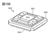
- 15A and 15B are diagrams illustrating an example of an electronic component.
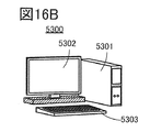
- 16A, 16B, 16C, 16D, 16E, and 16F are diagrams illustrating examples of electronic devices.
- 17A and 17B are diagrams illustrating examples of electronic devices.
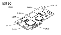
- 18A, 18B, and 18C are diagrams illustrating examples of electronic devices.
- FIG. 19 is a diagram showing various storage devices layer by layer.
- 20A and 20B are diagrams illustrating examples of electronic devices.
- film and the term “layer” can be interchanged with each other.
- conductive layer to the term “conductive film”.
- insulating film to the term “insulating layer”.
- gate electrode on the gate insulating layer does not exclude one including another component between the gate insulating layer and the gate electrode.
- the term “electrically connected” includes the case where they are connected via “an object having some electrical action”.
- the “object having some kind of electrical action” is not particularly limited as long as it can transfer an electric signal between the connection targets.
- things having some kind of electrical action include electrodes and wirings, switching elements such as transistors, resistance elements, inductors, capacitance elements, and other elements having various functions.
- switching elements such as transistors, resistance elements, inductors, capacitance elements, and other elements having various functions.
- electrode and “wiring” do not functionally limit these components.
- electrode may be used as part of “wiring” and vice versa.
- a “terminal” in an electric circuit refers to a portion where input or output of current or potential and reception (or transmission) of a signal are performed. Therefore, part of the wiring or the electrode may function as a terminal.
- the “capacitance” has a structure in which two electrodes face each other via an insulator (dielectric).
- the term “capacitance element” includes the above-mentioned “capacitance”. That is, in this specification and the like, the term “capacitance element” means that two electrodes face each other through an insulator, that two wirings face each other through an insulator, or The case where two wires are arranged via an insulator is included.
- the term “voltage” often refers to a potential difference between a certain potential and a reference potential (eg, a ground potential). Therefore, the voltage and the potential difference can be rephrased.
- a transistor is an element having at least three terminals including a gate, a drain, and a source.
- a channel formation region is provided between the drain (drain terminal, drain region, or drain electrode) and the source (source terminal, source region, or source electrode), and the source and drain are connected via the channel formation region. An electric current can be passed between them.
- a channel formation region refers to a region in which a current mainly flows.
- the functions of the source and the drain may be switched when a transistor of different polarity is used or when the direction of current changes in circuit operation. Therefore, in this specification and the like, the terms source and drain can be interchanged.
- off-state current refers to drain current when a transistor is in an off state (also referred to as a non-conducting state or a blocking state).
- the off-state is a state in which the gate voltage Vgs with respect to the source is lower than the threshold voltage Vth in the n-channel transistor, and the gate voltage Vgs with respect to the source in the p-channel transistor. It is a state higher than the threshold voltage Vth. That is, the off-state current of the n-channel transistor may be a drain current when the gate voltage Vgs with respect to the source is lower than the threshold voltage Vth.
- off-state current may refer to the source current when the transistor is off. Further, it may be referred to as a leak current in the same meaning as an off current. In this specification and the like, off-state current may refer to current flowing between a source and a drain when a transistor is in an off state.
- the on-state current may refer to a current flowing between a source and a drain when the transistor is in an on state (also referred to as a conductive state).
- a metal oxide is a metal oxide in a broad sense. Metal oxides are classified into oxide insulators, oxide conductors (including transparent oxide conductors), oxide semiconductors, and the like.
- the metal oxide when a metal oxide is used for a channel formation region of a transistor, the metal oxide may be referred to as an oxide semiconductor. That is, when the metal oxide has at least one of an amplifying action, a rectifying action, and a switching action, the metal oxide can be called a metal oxide semiconductor. That is, a transistor including a metal oxide in a channel formation region can be referred to as an “oxide semiconductor transistor” or an “OS transistor”.
- a metal oxide having nitrogen may be referred to as a metal oxide.
- the metal oxide containing nitrogen may be referred to as a metal oxynitride. Details of the metal oxide will be described later.
- a memory device is a memory device that can function by utilizing semiconductor characteristics and is also called a memory.
- the memory device has a structure in which a plurality of layers including OS transistors is stacked over a layer including transistors formed over a semiconductor substrate.
- FIG. 1 is a perspective view showing a configuration example of a storage device 10 according to one embodiment of the present invention.
- the memory device 10 includes a layer 100 and layers 200_1 to 200_1 (l is an integer of 1 or more).
- layers 200_1 to 200_1 l is an integer of 1 or more.
- reference numerals such as "_1" and [_2] are used to distinguish a plurality of elements having similar functions. That is, when referring to an arbitrary layer among the layers 200_1 to 200_1, the reference numeral of the layer 200 is used for description, and when it is necessary to specify one, reference numerals such as the layer 200_1 and the layer 200_2 are used. explain.
- the memory device 10 includes a layer 200_1 stacked over the layer 100, a layer 200_2 stacked over the layer 200_1, and the layers 200_3 (not shown) to
- the layer 200_1 also has a structure in which layers are stacked in order. Further, in order to make the explanation easy to understand, the case where l is 2 will be described hereinafter in the present embodiment.
- FIG. 2 is a schematic perspective view showing a configuration example of the storage device 10 according to one embodiment of the present invention.
- the memory device 10 illustrated in FIG. 2 includes a layer 100, a layer 200_1, and a layer 200_2, the layer 200_1 is stacked over the layer 100, and the layer 200_2 is stacked over the layer 200_1. ing.
- Each of the layer 100, the layer 200_1, and the layer 200_2 is provided with a circuit which can function by utilizing semiconductor characteristics.
- the layer 100 includes the peripheral circuit 101 and the layer 200_1 and the layer 200_1.
- a memory cell array 111 is provided in 200_2. Note that in the drawings described in this specification and the like, main signal flows are indicated by arrows or lines, and power supply lines and the like may be omitted.
- the peripheral circuit 101 has a row decoder 121, a word line driver circuit 122, a word line driver circuit 123, a column decoder 131, a bit line driver circuit 132, a page buffer 138, an output circuit 141, and a control logic circuit 151.
- the peripheral circuit 101 has a function as a drive circuit and a control circuit of the memory cell array 111.
- the peripheral circuit 101 is configured using transistors formed on the semiconductor substrate SUB.
- the semiconductor substrate SUB is not particularly limited as long as it can form the channel region of the transistor.
- a single crystal silicon substrate, a single crystal germanium substrate, a compound semiconductor substrate (SiC substrate, GaN substrate, etc.), an SOI (Silicon on Insulator) substrate, etc. can be used.
- the SOI substrate is formed by implanting oxygen ions into a mirror-polished wafer and then heating it at a high temperature to form an oxide layer at a certain depth from the surface and eliminate defects generated in the surface layer.
- An SOI substrate formed by the above may be used.
- a transistor formed using a single crystal substrate has a single crystal semiconductor in a channel formation region.
- a single crystal silicon substrate is used for the semiconductor substrate SUB.
- a transistor formed over a single crystal silicon substrate is called a Si transistor.
- the peripheral circuit 101 configured by using Si transistors can operate at high speed.
- the memory cell array 111 has a plurality of memory cells 112, and the memory cells 112 are configured using OS transistors. Since the OS transistor is a thin film transistor, the memory cell array 111 can be stacked over the semiconductor substrate SUB.
- the OS transistor since the band gap of the oxide semiconductor is 2.5 eV or more, preferably 3.0 eV or more, the OS transistor has a small leak current due to thermal excitation and an extremely small off current.
- the metal oxide used for the channel formation region of the OS transistor is preferably an oxide semiconductor containing at least one of indium (In) and zinc (Zn).
- a typical example of such an oxide semiconductor is an In-M-Zn oxide (the element M is Al, Ga, Y, or Sn).
- the oxide semiconductor can be i-type (intrinsic) or substantially i-type.
- Such an oxide semiconductor can be referred to as a highly purified oxide semiconductor. Note that details of the OS transistor will be described in Embodiment 3.
- the memory cell 112 has a function of storing data by accumulating and holding charges.
- the memory cell 112 may have a function of storing binary (high level or low level) data, or may have a function of storing four or more levels of data. Alternatively, it may have a function of storing analog data.
- the OS transistor Since the off-state current of the OS transistor is extremely small, the OS transistor is suitable as a transistor used for the memory cell 112.
- the OS transistor can have an off-state current per channel width of 1 ⁇ m of 100 zA/ ⁇ m or less, 10 zA/ ⁇ m or less, 1 zA/ ⁇ m or less, or 10 yA/ ⁇ m or less, for example.
- the OS transistor Since the OS transistor has a feature that the off-state current does not easily increase even at high temperature, the memory device 10 can operate even when the temperature of the environment where it is installed is high. In addition, the data stored in the memory cell 112 is less likely to be lost even under high temperature due to heat generation of the peripheral circuit 101. By using the OS transistor, the reliability of the memory device 10 can be improved.
- a transistor other than the OS transistor may be used as long as the off-state current is low.
- a transistor including a semiconductor with a wide bandgap in a channel formation region may be used.
- the semiconductor with a large band gap may refer to a semiconductor with a band gap of 2.2 eV or more, and examples thereof include silicon carbide, gallium nitride, and diamond.
- memory cells 112 are arranged in a matrix (also referred to as a matrix), and each memory cell 112 is electrically connected to a wiring WL and a wiring BL.
- the memory cell 112 is selected by the potential applied to the wiring WL, and data is written to the selected memory cell 112 through the wiring BL.
- the memory cell 112 is selected by the potential applied to the wiring WL and data is read from the selected memory cell 112 through the wiring BL. That is, the wiring WL functions as a word line of the memory cell 112 and the wiring BL functions as a bit line of the memory cell 112.
- the wiring WL and the wiring BL illustrated in FIG. 2 each include a plurality of wirings.
- the wiring WL includes a plate line PL, a write word line WWL, a read word line RWL, a wiring BG1, and a wiring BG2, and the wiring BL includes a read bit line RBL and a write bit line WBL. (See Figures 3 and 4).
- the memory cell array 111 provided in the layer 200_1 is electrically connected to the word line driver circuit 122 through the wiring WL, and the memory cell array 111 provided in the layer 200_2 is connected through the wiring WL in the word line driver circuit. It is electrically connected to 123.
- the memory cell array 111 provided in the layer 200_1 and the memory cell array 111 provided in the layer 200_2 are electrically connected to the bit line driver circuit 132 through the wiring BL.
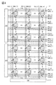
- FIG. 3 is a block diagram showing a configuration example of the storage device 10.
- the memory cell array 111 provided in the layer 200_2 and the word line driver circuit 123 are omitted, and only one memory cell 112 included in the memory cell array 111 is illustrated as a representative.
- the memory device 10 has a peripheral circuit 101 and a memory cell array 111.
- the peripheral circuit 101 has a row decoder 121, a word line driver circuit 122, a column decoder 131, a bit line driver circuit 132, a page buffer 138, an output circuit 141, and a control logic circuit 151.
- the memory cell array 111 includes a plurality of memory cells 112 (only one is shown in FIG. 3), and the memory cell 112 includes a plate line PL, a write word line WWL, a read word line RWL, a wiring BG1, and a wiring BG2.
- the bit line driver circuit 122 is electrically connected to the bit line driver circuit 122 via the read bit line RBL and the write bit line WBL.
- the potential Vss, the potential Vdd, the potential Vdh, the precharge potential Vpre, and the reference potential Vref are input to the memory device 10.
- the potential Vdh is the high power supply potential of the write word line WWL.
- a clock signal CLK, a chip enable signal CE, a global write enable signal GW, a byte write enable signal BW, an address signal ADDR, and a data signal WDATA are input to the memory device 10, and the memory device 10 outputs a data signal RDATA.
- these signals are digital signals represented by a high level or a low level (sometimes represented by High or Low, H or L, 1 or 0, etc.).
- a high level of a digital signal is represented by the potential Vdd and a low level thereof is represented by the potential Vss.
- the potential Vdh is used for the high level and the potential Vss is used for the low level of the write word line WWL.
- the byte write enable signal BW, the address signal ADDR, the data signal WDATA, and the data signal RDATA are signals having a plurality of bits.
- the byte write enable signal has BW[0] to BW[3], and when it is necessary to specify one bit, it is referred to as, for example, the byte write enable signal BW[0].
- the byte write enable signal BW[0] indicates an arbitrary bit.
- the byte write enable signal BW can be 4 bits, and the data signal WDATA and the data signal RDATA can be 32 bits. That is, the byte write enable signal BW, the data signal WDATA, and the data signal RDATA are the byte write enable signal BW[3:0], the data signal WDATA[31:0], and the data signal RDATA[31:0], respectively. It is written.
- the above-described circuits, signals, and potentials can be appropriately discarded as necessary.
- another circuit, another signal, or another potential may be added.
- the control logic circuit 151 processes the chip enable signal CE and the global write enable signal GW to generate control signals for the row decoder 121 and the column decoder 131. For example, when the chip enable signal CE is high level and the global write enable signal GW is low level, the row decoder 121 and the column decoder 131 perform a read operation, the chip enable signal CE is high level, and the global write enable signal GW is high level. In this case, the row decoder 121 and the column decoder 131 perform the write operation, and when the chip enable signal CE is at the low level, the row decoder 121 and the column decoder 131 are in the standby state regardless of the high level and the low level of the global write enable signal GW. It can be an action.
- the signal processed by the control logic circuit 151 is not limited to this, and another signal may be input as necessary.
- control logic circuit 151 processes the byte write enable signal BW[3:0] to control the write operation. Specifically, when the byte write enable signal BW[0] is at high level, the row decoder 121 and the column decoder 131 perform the write operation of the data signal WDATA[7:0]. Similarly, when the byte write enable signal BW[1] is at the high level, the write operation of the data signal WDATA[15:8] is performed. When the byte write enable signal BW[2] is at the high level, the data signal WDATA[23:16]. ], and when the byte write enable signal BW[3] is at a high level, the data signal WDATA[31:24] is written.
- the address signal ADDR is input to the row decoder 121 and the column decoder 131, in addition to the above-described control signal generated by the control logic circuit 151.
- the row decoder 121 decodes the address signal ADDR and generates a control signal for the word line driver circuit 122.
- the word line driver circuit 122 has a function of driving the plate line PL, the write word line WWL, the read word line RWL, the wiring BG1, and the wiring BG2, or a function of applying a predetermined potential.
- the word line driver circuit 122 selects the write word line WWL or the read word line RWL of the access target row based on the control signal of the row decoder 121.
- the word line driver circuit 122 may have a function of selecting the wiring BG1 or the wiring BG2.
- the predecoder 124 may be provided.
- the predecoder 124 has a function of decoding the address signal ADDR and determining a block to be accessed.
- the column decoder 131, the bit line driver circuit 132, and the page buffer 138 have a function of writing data input by the data signal WDATA into the memory cell array 111, a function of reading data from the memory cell array 111, and amplification and output of read data. It has a function of outputting to the circuit 141 and the like.
- the output circuit 141 outputs the data read from the memory cell array 111 by the column decoder 131 and the bit line driver circuit 132 and stored in the page buffer 138 as a data signal RDATA.
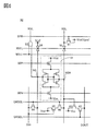
- the bit line driver circuit 132 has a precharge circuit 133, a sense amplifier circuit 134, an output MUX (multiplexer) circuit 135, and a write driver circuit 136.
- the precharge circuit 133, the sense amplifier circuit 134, the output MUX circuit 135, and the write driver circuit 136 will be described later.
- FIG. 4 is a block diagram showing a configuration example of the memory cell array 111.
- FIG. 4 shows two memory cell arrays 111, a word line driver circuit 122, a word line driver circuit 123, and a bit line driver circuit 132.
- the memory cell array 111 is a plate line PL and a write word line.
- the state where the memory cell array 111 is electrically connected to the bit line driver circuit 132 via the read bit line RBL and the write bit line WBL.
- the memory cell array 111 electrically connected to the word line driver circuit 122 through the wiring WL is the memory cell array 111 provided in the layer 200_1 and electrically connected to the word line driver circuit 123 through the wiring WL.
- the memory cell array 111 connected to is the memory cell array 111 provided in the layer 200_2.
- One memory cell array 111 has m (m is an integer of 1 or more) in one column, n (n is an integer of 1 or more) in one row, and a total of m ⁇ n memory cells 112. They are arranged in a matrix. Although the same memory cell array 111 is provided in the layer 200_1 and the layer 200_2 in FIG. 4, the memory cell array 111 provided in the layer 200_1 and the memory cell array 111 provided in the layer 200_2 have memory cells. The number of 112 and the like may be different.
- the address of the memory cell 112 is also shown, and [1,1], [i,1], [m,1], [1,j], [i,j], [m,j]. , [1, n], [i, n], [m, n] (i is an integer of 1 or more and m or less, j is an integer of 1 or more and n or less) are addresses of the memory cell 112.
- the memory cell 112 described as [i,j] is the memory cell 112 arranged in the i-th row and the j-th column.
- the memory cell 112 arranged in the i-th row and the j-th column has a plate line PL[i], a write word line WWL[i], a read word line RWL[i], a wiring BG1[i], a wiring BG2[i], a read bit.
- the line RBL[j] and the write bit line WBL[j] are electrically connected.
- the memory cells 112 arranged in the i-th row and the j-th column include the plate line PL[i], the write word line WWL[i], the read word line RWL[i], the wiring BG1[i], and the wiring BG2[i. ]
- the memory device 10 includes 2 ⁇ m plate lines PL, 2 ⁇ m write word lines WWL, 2 ⁇ m read word lines RWL, 2 ⁇ m wirings BG1, and 2 ⁇ m wirings. It has BG2, n read bit lines RBL, and n write bit lines WBL.
- FIG. 5A is a circuit diagram showing a configuration example of the memory cell 112.
- the memory cell 112 has a transistor 11, a transistor 12, and a capacitor C11.
- the transistor 11 may be referred to as a writing transistor and the transistor 12 may be referred to as a reading transistor.
- the transistors 11 and 12 each have a front gate (sometimes referred to simply as a gate) and a back gate.
- One of the source and the drain of the transistor 11 is electrically connected to the write bit line WBL, and the other of the source and the drain of the transistor 11 is electrically connected to the front gate of the transistor 12 and one terminal of the capacitor C11.
- the front gate of the transistor 11 is electrically connected to the write word line WWL, and the back gate of the transistor 11 is electrically connected to the wiring BG1.
- One of the source and the drain of the transistor 12 is electrically connected to the read bit line RBL, the other of the source and the drain of the transistor 12 is electrically connected to the read word line RWL, and the back gate of the transistor 12 is the wiring BG2. Electrically connected to.
- the other terminal of the capacitive element C11 is electrically connected to the plate line PL.
- the wiring BG1 functions as a wiring for applying a predetermined potential to the back gate of the transistor 11
- the wiring BG2 functions as a wiring for applying a predetermined potential to the back gate of the transistor 12.
- the plate line PL functions as a wiring for applying a predetermined potential to the other terminal of the capacitive element C11.
- a connection portion in which the other of the source and the drain of the transistor 11, the front gate of the transistor 12, and one terminal of the capacitor C11 are electrically connected is referred to as a node N11.
- the transistor 11 has a function as a switch for electrically connecting or disconnecting the node N11 and the write bit line WBL.
- the memory cell 112 may have a configuration that does not have the capacitive element C11.
- Data writing is performed by applying a high-level potential to the write word line WWL to make the transistor 11 conductive and electrically connecting the node N11 and the write bit line WBL. Specifically, when the transistor 11 is conductive, a potential corresponding to the data to be written is applied to the write bit line WBL and the potential is written to the node N11. After that, a low-level potential is applied to the write word line WWL and the transistor 11 is turned off, so that the potential of the node N11 is held.
- a predetermined potential is applied to the read bit line RBL, then the read bit line RBL is electrically floated, and a low-level potential is applied to the read word line RWL. Done.
- applying a predetermined potential to the read bit line RBL and then bringing the read bit line RBL into a floating state is referred to as precharging the read bit line RBL.
- the transistor 12 has a potential difference between the source and the drain, and the current flowing between the source and the drain of the transistor 12 is held in the node N11. It depends on the potential. Therefore, the potential held in the node N11 can be read by reading the potential change of the read bit line RBL when the read bit line RBL is in a floating state.
- the row in which the memory cell 112 for writing data is arranged is selected by the write word line WWL for applying a high-level potential, and the row in which the memory cell 112 for reading data is arranged has a low-level potential. It is selected by the read word line RWL to be applied. On the contrary, the row in which the memory cell 112 in which data is not written is arranged applies the low level potential to the write word line WWL, and the row in which the memory cell 112 in which data is not read is arranged is the read word line RWL. By applying the same potential as the precharge potential to the read bit line RBL, it can be made unselected.
- the memory cell 112 can store data by accumulating and retaining charges in the node N11.
- the node N11 can store binary data.
- the memory cell 112 is a gain cell type memory cell including two-transistor one-capacitance element (or two-transistor).
- the gain cell type memory cell can operate as a memory by amplifying the accumulated charge with the nearest transistor even if the charge accumulation capacity is small.
- the memory cell 112 is the NOSRAM described above.
- the transistors 11 and 12 are transistors (OS transistors) each including a metal oxide in a channel formation region.
- OS transistors transistors
- the transistors 11 and 12 indium, an element M (the element M is aluminum, gallium, yttrium, copper, vanadium, beryllium, boron, titanium, iron, nickel, germanium, zirconium, molybdenum, lanthanum,
- a metal oxide having any one of cerium, neodymium, hafnium, tantalum, tungsten, magnesium, or the like) and zinc can be used.
- a metal oxide composed of indium, gallium and zinc is preferable.
- the off-state current of the OS transistor is extremely small, the potential written in the node N11 can be held for a long time by using the OS transistor as the transistor 11. That is, the data written in the memory cell 112 can be retained for a long time.
- the capacitance of the capacitor C11 can be reduced.
- the capacitive element C11 the gate capacitance of a transistor, the parasitic capacitance of wiring, or the like can be used. Therefore, in the memory cell 112, it is not necessary to form a capacitor element separately from a transistor or a wiring, and the memory cell 112 may have a structure without the capacitor element C11. With the structure in which the memory cell 112 does not include the capacitor C11, the area of the memory cell 112 can be reduced.
- the memory cell array 111 can be stacked over the peripheral circuit 101 by using OS transistors for the transistors 11 and 12.
- the threshold voltage of the transistors 11 and 12 is increased or decreased. can do.
- the threshold voltage shifts to a negative value, and the potential applied to the back gates of the transistors 11 and 12 is lowered.
- the threshold voltage shifts to the plus.
- the on-state current of the transistor can be increased and the memory cell 112 can operate at high speed.
- shifting the threshold voltage to plus off-state current of the transistor can be reduced and the memory cell 112 can hold data for a long time.
- the back gate of the transistor 11 is electrically connected to the wiring BG1 and the back gate of the transistor 12 is electrically connected to the wiring BG2, the potential applied to the wiring BG1 is lowered.
- the off-state current of the transistor 11 can be reduced, and the on-state current of the transistor 12 can be increased by increasing the potential applied to the wiring BG2.
- the transistor 11 and the transistor 12 can be transistors for each purpose.
- the wiring BG1 and the wiring BG2 may be integrated into one wiring, and the same potential may be applied to the back gate of the transistor 11 and the back gate of the transistor 12.
- the wiring BG2 may be driven using the word line driver circuit 122 or the word line driver circuit 123.
- the word line driver circuit 122 or the word line driver circuit 123 can increase the on-state current of the transistor 12 in the reading operation by increasing the potential applied to the wiring BG2 in the row to be read. On the contrary, by applying a low potential to the wiring BG2 other than the row to be read, the off-state current of the transistor 12 which is not performing the reading operation can be reduced.
- the read operation of the memory cell 112 is increased and the off-state current of the transistor 12 included in the other memory cells 112 is reduced. By doing so, the current leaking to the read bit line RBL can be reduced. The accuracy of the read operation can be improved by reducing the current leaking to the read bit line RBL.
- FIG. 5B is a circuit diagram showing a configuration example of the memory cell 113.
- the memory cell 113 has a transistor 11, a transistor 12, and a capacitor C11.
- One of the source and the drain of the transistor 11 is electrically connected to the write bit line WBL, and the other of the source and the drain of the transistor 11 is the other of the front gate of the transistor 12, the back gate of the transistor 12, and one of the capacitor C11. , And the front gate of the transistor 11 is electrically connected to the write word line WWL and the back gate of the transistor 11.
- One of the source and the drain of the transistor 12 is electrically connected to the read bit line RBL, and the other of the source and the drain of the transistor 12 is electrically connected to the read word line RWL.
- the other terminal of the capacitive element C11 is electrically connected to the plate line PL.
- the on-state current of the transistor 11 can be increased.
- the on-state current of the transistor 12 can be increased. That is, the memory cell 113 can operate at high speed.
- each of the transistor 11 and the transistor 12 may be a transistor having no back gate.
- the manufacturing process of the transistor can be simplified.
- FIG. 6 is a circuit diagram showing a configuration example of the circuit 50.
- the circuit 50 includes transistors 61 to 66, a sense amplifier circuit 51, an AND circuit 52, an analog switch 53, and an analog switch 54.
- the circuit 50 operates according to the signal SEN, the signal SEP, the signal BPR, the signal RSEL[3:0], the signal WSEL, the signal GRSEL[3:0], and the signal GWSEL[15:0]. It should be noted that one of the 4-bit signals RSEL[3:0] is input to one circuit 50. The same applies to other signals having a plurality of bits (GRSEL[3:0] etc.).
- the data DIN[31:0] is written to the memory cell array 111 and the data DOUT[31:0] is read from the memory cell array 111 by the bit line driver circuit 132.
- One circuit 50 writes any 1-bit data of the 32-bit data DIN [31:0] to the memory cell array 111, and writes any 1-bit data of the 32-bit data DOUT [31:0]. It has a function of reading data from the memory cell array 111.
- the data DIN[31:0] and the data DOUT[31:0] are internal signals, and the data DIN[31:0] are signals supplied from the page buffer 138 to the bit line driver circuit 132.
- DOUT[31:0] is a signal output from the bit line driver circuit 132 to the page buffer 138.
- a data signal WDATA is input to the page buffer 138 from the outside of the storage device 10, and the page buffer 138 outputs the data signal RDATA to the outside of the storage device 10 via the output circuit 141.
- the page buffer 138 can store at least a data amount (n bits) that can be stored in one row in the memory cell array 111. In this embodiment, it is preferable that data of 128 bits or more can be stored.
- the transistor 61 constitutes the precharge circuit 133.
- the read bit line RBL is precharged to the precharge potential Vpre by the transistor 61. Note that in this embodiment, the case where the potential Vdd (high level) is used as the precharge potential Vpre is described (in FIG. 6 and FIG. 7, written as Vdd (Vpre)).
- the signal BPR is a precharge signal, and the conduction state of the transistor 61 is controlled by the signal BPR.
- the sense amplifier circuit 51 constitutes a sense amplifier circuit 134.
- the sense amplifier circuit 51 determines the high level or the low level of the data input to the read bit line RBL during the read operation.
- the sense amplifier circuit 51 also functions as a latch circuit that temporarily holds the data DIN input from the write driver circuit 136 during the write operation.
- the sense amplifier circuit 51 shown in FIG. 6 is a latch type sense amplifier.
- the sense amplifier circuit 51 has two inverter circuits, and the input node of one inverter circuit is connected to the output node of the other inverter circuit.
- the input node of one of the inverter circuits is node NS and the output node is node NSB, complementary data is held at nodes NS and NSB.
- the signal SEN and the signal SEP are sense amplifier enable signals for activating the sense amplifier circuit 51, and the reference potential Vref is a read determination potential.
- the sense amplifier circuit 51 determines, with reference to the reference potential Vref, whether the potential of the node NSB at the time of activation is high level or low level.
- the AND circuit 52 controls the conduction state between the node NS and the write bit line WBL.
- the analog switch 53 controls the conduction state between the node NSB and the read bit line RBL, and the analog switch 54 controls the conduction state between the node NS and the wiring that supplies the reference potential Vref.
- the potential of the read bit line RBL is transmitted to the node NSB by the analog switch 53, and when the potential of the read bit line RBL becomes lower than the reference potential Vref, the sense amplifier circuit 51 determines that the read bit line RBL is at the low level. To do. When the potential of the read bit line RBL does not become lower than the reference potential Vref, the sense amplifier circuit 51 determines that the read bit line RBL is at high level.
- the signal WSEL is a write selection signal and controls the AND circuit 52.
- the signals RSEL[3:0] are read selection signals and control the analog switch 53 and the analog switch 54.
- the transistor 62 and the transistor 63 form an output MUX circuit 135.
- the signals GRSEL[3:0] are global read selection signals and control the output MUX circuit 135.
- the output MUX circuit 135 has a function of selecting 32 read bit lines RBL from which data is read out of 128 read bit lines RBL.
- the output MUX circuit 135 functions as a multiplexer with 128 inputs and 32 outputs.
- the output MUX circuit 135 reads the data DOUT[31:0] from the sense amplifier circuit 134 and outputs it to the page buffer 138.
- the transistors 64 to 66 form a write driver circuit 136.
- the signals GWSEL[15:0] are global write selection signals and control the write driver circuit 136.
- the write driver circuit 136 has a function of writing the data DIN[31:0] to the sense amplifier circuit 134.
- the write driver circuit 136 has a function of selecting a column to which the data DIN[31:0] is written.
- the write driver circuit 136 writes data in byte units, half word units, or 1 word units according to the signal GWSEL [15:0].
- the circuit 50 is electrically connected to the data DIN[h] (h is an integer of 0 or more and 31 or less) every four columns.
- the circuit 50 is electrically connected to the data DOUT[h] every four columns.
- FIG. 7 is a timing chart illustrating an operation example of the memory cell 112.
- the potential relationship between the write word line WWL, the read word line RWL, the read bit line RBL, and the write bit line WBL in the write operation and the read operation of the memory cell 112 will be described. Further, a case where the wiring BG2 is driven using the word line driver circuit 122 or the word line driver circuit 123 will be described later.
- a period Twrite is a period in which a writing operation is performed and a period Tread is a period in which a reading operation is performed.
- the high level of the read word line RWL, the read bit line RBL, and the write bit line WBL is the potential Vdd, and the low level thereof is the potential Vss.
- the high level of the write word line WWL is the potential Vdh, and the low level of the write word line WWL is the potential Vss.
- the potential Vdd is applied to the read word line RWL and the read bit line RBL.
- the read bit line RBL is precharged with the potential Vdd.
- the potential Vss is applied to the read word line RWL of the row in which the memory cell 112 for reading data is arranged while the read bit line RBL is in the floating state, when the data written in the node N11 is high level, the transistor 12 becomes conductive, and the potential of the read bit line RBL starts to drop.
- the sense amplifier circuit 51 determines that the read bit line RBL is at the low level.
- the sense amplifier circuit 51 determines that the read bit line RBL is at high level.
- the potential Vss is applied to the write bit line WBL and the write word line WWL.
- the high level of the wiring BG2 can be set to the potential Vdh and the low level of the wiring BG2 can be set to the potential Vss.
- the potential Vss is applied to the wiring BG2
- the potential Vdh is applied to the wiring BG2 in the row where the memory cell 112 from which data is read is arranged.
- the on-state current of the transistor 12 included in the memory cell 112 from which data is read can be increased. Further, the potential Vss is applied to the wiring BG2, so that the off-state current of the transistor 12 can be reduced.
- the memory device 10 has a gain cell type memory cell composed of n-channel type transistors, and the write word line WWL, the read word line RWL, the write bit line WBL, and the read bit line RBL are A high level or a low level is represented by three types of potentials (potential Vss, potential Vdd, and potential Vdh). That is, the storage device 10 can be operated with a small number of power sources, and the cost of an electronic device equipped with the storage device 10 can be reduced.
- the gain cell type memory cell requires at least two transistors per memory cell, and it was difficult to increase the number of memory cells that can be arranged per unit area.
- OS transistors are used as the transistors forming the memory cell 112.
- a plurality of memory cell arrays 111 can be stacked and provided on the semiconductor substrate SUB on which the peripheral circuit 101 is formed. That is, the amount of data that can be stored per unit area can be increased.
- the gain cell type memory cell can operate as a memory by amplifying the accumulated charge with the nearest transistor even when the charge accumulation capacity is small. Furthermore, the capacity of the capacitor C11 can be reduced by using an OS transistor whose off-state current is extremely low as a transistor included in the memory cell 112. Alternatively, a gate capacitance of a transistor, a parasitic capacitance of a wiring, or the like can be used as the capacitor C11, and the capacitor C11 can be omitted. That is, the area of the memory cell 112 can be reduced.
- FIG. 8A and 8B illustrate a structure of the memory cell 860 included in the memory device according to one embodiment of the present invention.
- FIG. 8A is a top view of the periphery of the memory cell 860.
- 8B is a cross-sectional view of the memory cell 860, and FIG. 8B corresponds to a portion indicated by a dashed-dotted line A1-A2 in FIG. 8A.
- 8B shows a cross section in the channel length direction of the transistor 600 and a cross section in the channel width direction of the transistor 700.
- the X direction, the Y direction, and the Z direction shown in FIG. 8A are directions orthogonal to or intersecting with each other.
- the X direction and the Y direction are parallel or substantially parallel to the substrate surface
- the Z direction is perpendicular or substantially vertical to the substrate surface.
- the memory cell 860 described in this embodiment includes a transistor 600, a transistor 700, and a capacitor 655.
- the memory cell 860 corresponds to the memory cell 112 described in the above embodiment, and the transistor 600, the transistor 700, and the capacitor 655 are the transistor 11, the transistor 12, and the capacitor described in the above embodiment, respectively. It corresponds to the element C11. Therefore, one of the source and the drain of the transistor 600, the gate of the transistor 700, and one of the electrodes of the capacitor 655 are electrically connected to each other.
- the transistor 600 and the transistor 700 are provided over the insulator 614, and the insulator 680 is provided over part of the transistor 600 and the transistor 700.
- An insulator 682 is placed over the 600, the transistor 700, and the insulator 680, an insulator 685 is placed over the insulator 682, a capacitor 655 is placed over the insulator 685, and a capacitor 655 is placed over the capacitor 655.
- An insulator 688 is placed.
- the insulator 614, the insulator 680, the insulator 682, the insulator 685, and the insulator 688 function as an interlayer film.
- the transistor 600 includes an insulator 616 over an insulator 614, a conductor 605 (a conductor 605 a, and a conductor 605 b) which is arranged so as to be embedded in the insulator 616, over the insulator 616, and a conductor.
- Insulator 622 over body 605, insulator 624 over insulator 622, oxide 630a over insulator 624, oxide 630b over oxide 630a, oxide 643a over oxide 630b, and oxide.
- the oxide 630c is in contact with the side surface of the oxide 643a, the side surface of the oxide 643b, the side surface of the conductor 642a, and the side surface of the conductor 642b, respectively.
- the top surface of the conductor 660 is arranged to be substantially aligned with the top surface of the insulator 650, the top surface of the oxide 630c, and the top surface of the insulator 680.
- the insulator 682 is in contact with the top surfaces of the conductor 660, the insulator 650, the oxide 630c, and the insulator 680, respectively.
- the oxide 630a, the oxide 630b, and the oxide 630c may be collectively referred to as the oxide 630.
- the oxide 643a and the oxide 643b may be collectively referred to as the oxide 643.
- the conductor 642a and the conductor 642b may be collectively referred to as a conductor 642.
- the conductor 660 functions as a gate, and the conductors 642a and 642b function as a source and a drain, respectively. Further, the conductor 605 functions as a back gate.
- the transistor 600 is formed in a self-aligned manner so that the conductor 660 functioning as a gate fills the opening formed by the insulator 680 or the like. As described above, in the memory device according to this embodiment, the conductor 660 can be reliably arranged in the region between the conductor 642a and the conductor 642b without alignment.
- the transistor 700 includes the insulator 616 over the insulator 614, the conductor 705 (the conductor 705a, and the conductor 705b) arranged so as to be embedded in the insulator 616, the insulator 616, and the conductor 705.
- the oxide 730c, the insulator 750 over the oxide 730c, and the conductor 760 (the conductor 760a and the conductor 760b) which is located over the insulator 750 and overlaps with the oxide 730c.
- the oxide 730c is in contact with the side surface of the oxide 743a, the side surface of the oxide 743b, the side surface of the conductor 742a, and the side surface of the conductor 742b, respectively.
- the top surface of the conductor 760 is arranged to be substantially aligned with the top surface of the insulator 750, the top surface of the oxide 730c, and the top surface of the insulator 680.
- the insulator 682 is in contact with the top surfaces of the conductor 760, the insulator 750, the oxide 730c, and the insulator 680, respectively.
- the oxide 730a, the oxide 730b, and the oxide 730c may be collectively referred to as the oxide 730.
- the oxide 743a and the oxide 743b may be collectively referred to as an oxide 743.
- the conductor 742a and the conductor 742b may be collectively referred to as a conductor 742.
- the conductor 760 functions as a gate, and the conductors 742a and 742b function as a source and a drain, respectively.
- the conductor 705 functions as a back gate.
- the transistor 700 is formed in a self-aligned manner so that the conductor 760 functioning as a gate fills the opening formed by the insulator 680 or the like. As described above, in the memory device according to this embodiment, the conductor 760 can be reliably arranged in the region between the conductor 742a and the conductor 742b without alignment.
- the transistor 700 is formed in the same layer as the transistor 600 and has a similar structure. Therefore, although a cross section in the channel length direction of the transistor 700 is not illustrated, it has a structure similar to that of the transistor 600 in the channel length direction illustrated in FIG. 8B. That is, the oxide 743 and the conductor 742, which are not illustrated in the cross-sectional view, also have the same structure as the oxide 643 and the conductor 642 illustrated in FIG. 8B. Note that although a cross section in the channel width direction of the transistor 600 is not illustrated, it has a structure similar to that of the transistor 700 in the channel width direction illustrated in FIG. 8B.
- the oxide 730 has a structure similar to that of the oxide 630, and the description of the oxide 630 can be referred to.
- the conductor 705 has a structure similar to that of the conductor 605, and the description of the conductor 605 can be referred to.
- the oxide 743 has a structure similar to that of the oxide 643, and the description of the oxide 643 can be referred to.
- the conductor 742 has a structure similar to that of the conductor 642, and the description of the conductor 642 can be referred to.
- the insulator 750 has a structure similar to that of the insulator 650, and the description of the insulator 650 can be referred to.
- the conductor 760 has a structure similar to that of the conductor 660, and the description of the conductor 660 can be referred to. Unless otherwise specified, the description of the structure of the transistor 600 can be referred to for the structure of the transistor 700 as described above.
- a metal oxide functioning as an oxide semiconductor (hereinafter also referred to as an oxide semiconductor) is preferably used for the oxide 630 and the oxide 730 including a channel formation region.
- an energy gap of 2 eV or more, preferably 2.5 eV or more is preferably used.
- an In-M-Zn oxide (the element M is aluminum, gallium, yttrium, tin, copper, vanadium, beryllium, boron, titanium, iron, nickel, germanium, zirconium, molybdenum, lanthanum, cerium).
- the element M is preferably aluminum, gallium, yttrium, or tin.
- an In-M oxide, an In-Zn oxide, or an M-Zn oxide may be used as the oxide semiconductor.
- the transistors 600 and 700 each including an oxide semiconductor in the channel formation region have extremely low leakage current (off-state current) in the non-conduction state, and thus can provide a memory device with low power consumption. Further, the off-state current of the transistors 600 and 700 hardly increases even in a high temperature environment. Specifically, the off-state current hardly increases even at an ambient temperature of room temperature or higher and 200° C. or lower. Therefore, the operation is stable even in a high temperature environment, and a highly reliable storage device can be realized.
- the capacitance value of the capacitor 655 can be set small. As a result, the area occupied by the memory cell 860 can be reduced and the memory device can be integrated.
- the conductor 742a, the conductor 660, the conductor 605, and the conductor 705 preferably extend in the Y direction.
- the conductor 742a functions as the read word line RWL described in the above embodiment.
- the conductor 660 functions as the write word line WWL described in the above embodiment.
- the conductor 605 functions as the wiring BG1 described in the above embodiment.
- the conductor 705 functions as the wiring BG2 described in the above embodiment.
- the capacitor 655 includes a conductor 646a over the insulator 685, an insulator 686 that covers the conductor 646a, and a conductor 656 that is provided over the insulator 686 so as to overlap with at least part of the conductor 646a.
- the conductor 646 a functions as one electrode of the capacitor 655 and the conductor 656 functions as the other electrode of the capacitor 655.
- the insulator 686 functions as a dielectric of the capacitor 655.
- the conductor 656 extend in the Y direction and function as the plate line PL described in any of the above embodiments.
- openings are formed in the insulator 672, the insulator 673, the insulator 680, the insulator 682, and the insulator 685, and the conductor 640 serving as a plug (the conductor 640a, the conductor 640b, the conductor 640c, And a conductor 640d) is provided to be embedded in the opening. Further, the conductor 640 is provided so as to be exposed on the upper surface of the insulator 685.
- the conductor 640a has a lower surface in contact with the conductor 642a and an upper surface in contact with the conductor 646a.
- the lower surface of the conductor 640c is in contact with the conductor 760 and the upper surface is in contact with the conductor 646a. In this manner, one of the source and the drain of the transistor 600, the gate of the transistor 700, and one of the electrodes of the capacitor 655 are electrically connected.
- the lower surface of the conductor 640b is provided in contact with the conductor 642b. Further, a conductor 646b is provided in contact with the top surface of the conductor 640b.
- the conductor 646b is formed in the same layer as the conductor 646a and has a similar structure. As shown in FIG. 8A, the conductor 646b preferably extends in the X direction. With such a structure, the conductor 646b functions as the write bit line WBL described in the above embodiment.
- the lower surface of the conductor 640d is provided in contact with the conductor 742b. Further, a conductor 746 is provided in contact with the top surface of the conductor 640d.
- the conductor 746 is formed in the same layer as the conductor 646a and has a similar structure. As shown in FIG. 8A, the conductor 746 preferably extends in the X direction. With such a structure, the conductor 746 functions as the read bit line RBL described in any of the above embodiments.
- the transistor 600 and the transistor 700 can be formed in the same step; therefore, the manufacturing process of the memory device can be shortened and productivity can be improved. Can be made.
- the transistor 600, the transistor 700, and the capacitor 655 are provided so that the channel length direction of the transistor 600 and the channel width direction of the transistor 700 are parallel to each other. Is not limited to this.
- a memory cell 860 illustrated in FIG. 8 and the like is an example of a structure of a memory device, and a transistor, a capacitor, or the like having an appropriate structure may be arranged as appropriate depending on a circuit structure or a driving method.
- the oxide 630 is provided over the oxide 630a over the insulator 624, the oxide 630b over the oxide 630a, and the oxide 630b, and at least part of the oxide 630 is over the oxide 630b.
- the oxide 630c in contact therewith is preferable.
- the side surface of the oxide 630c is preferably provided in contact with the oxide 643a, the oxide 643b, the conductor 642a, the conductor 642b, the insulator 672, the insulator 673, and the insulator 680.
- oxide 630a By having the oxide 630a below the oxide 630b, diffusion of impurities from the structure formed below the oxide 630a into the oxide 630b can be suppressed. In addition, by having the oxide 630c over the oxide 630b, diffusion of impurities into the oxide 630b from a structure formed above the oxide 630c can be suppressed.
- the transistor 600 has a structure in which three layers of the oxide 630a, the oxide 630b, and the oxide 630c are stacked in the channel formation region and the vicinity thereof, the present invention is not limited to this. ..
- a single layer of the oxide 630b, a two-layer structure of the oxide 630b and the oxide 630a, a two-layer structure of the oxide 630b and the oxide 630c, or a stacked structure of four or more layers may be provided.
- the oxide 630c may have a two-layer structure and a four-layer stacked structure may be provided.
- the oxide 630 preferably has a stacked structure of a plurality of oxide layers in which the atomic ratio of each metal atom is different.
- the atomic ratio of the element M in the constituent elements is higher than the atomic ratio of the element M in the constituent elements in the metal oxide used for the oxide 630b. It is preferable.
- the atomic ratio of the element M to In is preferably higher than the atomic ratio of the element M to In in the metal oxide used for the oxide 630b.
- the atomic ratio of In to the element M is preferably higher than the atomic ratio of In to the element M in the metal oxide used for the oxide 630a.
- a metal oxide that can be used for the oxide 630a or the oxide 630b can be used. Note that in the metal oxide used for the oxide 630c, the atomic ratio of In to the element M may be higher than that in the metal oxide used for the oxide 630b.
- a metal oxide having a composition of [atomic ratio] or its vicinity may be used.
- an In oxide may be used as the oxide 630b.
- a material that can be used for the oxide 630b may be applied to the oxide 630c and the oxide 630c may be provided as a single layer or a stacked layer.
- the oxides 630b and 630c it is preferable to increase the ratio of indium in the film because the on-state current, field-effect mobility, or the like of the transistor can be increased. Further, the above-mentioned composition in the vicinity includes a range of ⁇ 30% of a desired atomic number ratio.
- the oxide 630b may have crystallinity.
- a CAAC-OS c-axis aligned crystalline oxide semiconductor
- An oxide having crystallinity such as CAAC-OS has few impurities and defects (such as oxygen vacancies) and has a high crystallinity and a dense structure. Therefore, extraction of oxygen from the oxide 630b by the source electrode or the drain electrode can be suppressed. Further, even if heat treatment is performed, oxygen can be reduced from being extracted from the oxide 630b, so that the transistor 600 is stable against a high temperature (so-called thermal budget) in a manufacturing process.
- the oxide 630c is preferably provided in the opening provided in the interlayer film including the insulator 680. Therefore, the insulator 650 and the conductor 660 have a region overlapping with the stacked-layer structure of the oxide 630b and the oxide 630a with the oxide 630c interposed therebetween. With such a structure, the oxide 630c and the insulator 650 can be formed by continuous film formation; therefore, the interface between the oxide 630 and the insulator 650 can be kept clean. Therefore, the influence of interface scattering on carrier conduction is reduced, and the transistor 600 can obtain high on-state current and high frequency characteristics.
- An oxide semiconductor having a low carrier concentration is preferably used for the oxide 630 (eg, the oxide 630b).
- the concentration of impurities in the oxide semiconductor may be lowered and the density of defect states may be lowered.
- low impurity concentration and low defect level density are referred to as high-purity intrinsic or substantially high-purity intrinsic.
- impurities in the oxide semiconductor include hydrogen, nitrogen, alkali metals, alkaline earth metals, iron, nickel, silicon, and the like.
- an oxide semiconductor reacts with oxygen which is bonded to a metal atom to be water, which might cause oxygen deficiency (also referred to as V 2 O 3 ) in the oxide semiconductor.
- oxygen deficiency also referred to as V 2 O 3
- a defect in which hydrogen is contained in an oxygen vacancy functions as a donor and an electron which is a carrier may be generated.
- part of hydrogen may be bonded to oxygen which is bonded to a metal atom to generate an electron which is a carrier. Therefore, a transistor including an oxide semiconductor which contains a large amount of hydrogen is likely to have normally-on characteristics. Further, hydrogen in the oxide semiconductor is likely to move due to stress such as heat and an electric field; therefore, when a large amount of hydrogen is contained in the oxide semiconductor, reliability of the transistor might be deteriorated.
- V OH can function as a donor of an oxide semiconductor.
- the oxide semiconductor may be evaluated not by the donor concentration but by the carrier concentration. Therefore, in this specification and the like, a carrier concentration which is assumed to be a state where no electric field is applied may be used as a parameter of the oxide semiconductor, instead of the donor concentration. That is, the “carrier concentration” described in this specification and the like can be called the “donor concentration” in some cases.
- the V O H to obtain a sufficiently reduced oxide semiconductor, the moisture in the oxide semiconductor, to remove impurities such as hydrogen (dehydration, may be referred to as dehydrogenation)
- the V O H oxide semiconductor impurity is sufficiently reduced such by using a channel formation region of the transistor, it is possible to have stable electrical characteristics.
- the hydrogen concentration of the oxide 630b obtained by secondary ion mass spectrometry is less than 1 ⁇ 10 20 atoms/cm 3 , and preferably less than 1 ⁇ 10 19 atoms/cm 3 . It can be preferably less than 5 ⁇ 10 18 atoms/cm 3 , and more preferably less than 1 ⁇ 10 18 atoms/cm 3 .
- the oxide 630 in which impurities such as hydrogen are sufficiently reduced in the channel formation region of the transistor 600 normally-off characteristics can be obtained, stable electrical characteristics can be obtained, and reliability can be improved. it can.
- the carrier concentration of the oxide semiconductor in the region functioning as a channel formation region is preferably 1 ⁇ 10 18 cm ⁇ 3 or lower, and 1 ⁇ 10 17 cm ⁇ 3. Less than 1 ⁇ 10 16 cm ⁇ 3 , more preferably less than 1 ⁇ 10 13 cm ⁇ 3 , still more preferably less than 1 ⁇ 10 12 cm ⁇ 3. More preferable. Note that there is no particular limitation on the lower limit of the carrier concentration of the oxide semiconductor in the region functioning as a channel formation region, but it can be set to, for example, 1 ⁇ 10 ⁇ 9 cm ⁇ 3 .
- a material that suppresses diffusion of impurities (hereinafter also referred to as a barrier material against impurities) is used and impurities such as hydrogen are used.
- a barrier property is a function of suppressing diffusion of a corresponding substance (also referred to as low permeability).
- the corresponding substance has a function of capturing and fixing (also referred to as gettering).
- an insulating film having a barrier property may be referred to as a barrier insulating film.
- silicon nitride or silicon nitride oxide has a high barrier property against hydrogen, it is preferably used as a sealing material.
- metal oxides such as aluminum oxide, hafnium oxide, gallium oxide, and indium gallium zinc oxide can be given.
- the insulator 614 aluminum oxide, hafnium oxide, or the like is preferably used.
- impurities such as water or hydrogen can be suppressed from diffusing from the substrate side to the transistor 600 side.
- oxygen contained in the insulator 624 and the like can be suppressed from diffusing to the substrate side.
- the conductor 605 is arranged so as to overlap with the oxide 630 and the conductor 660. Further, the conductor 605 is preferably provided by being embedded in the insulator 616.
- the potential applied to the conductor 605 is changed independently without being linked with the potential applied to the conductor 660, so that the threshold voltage (Vth ) Can be controlled.
- Vth threshold voltage
- Vth of the transistor 600 can be further increased and off-state current can be reduced. Therefore, applying a negative potential to the conductor 605 can reduce the drain current when the potential applied to the conductor 660 is 0 V, as compared to the case where no potential is applied.
- the conductor 605 is preferably provided larger than the size of a region of the oxide 630 which does not overlap with the conductors 642a and 642b.
- the conductor 605 preferably extends in a region outside the end portion of the oxide 630 which intersects with the channel width direction. That is, it is preferable that the conductor 605 and the conductor 660 overlap with each other with the insulator provided outside the side surface of the oxide 630 in the channel width direction.
- charge-up local charging
- the conductor 605 may overlap with at least the oxide 630 located between the conductor 642a and the conductor 642b.
- the height of the bottom surface of the conductor 660 in a region where the oxide 630a and the oxide 630b do not overlap with the conductor 660 is lower than that of the bottom surface of the oxide 630b.
- the conductor 660 functioning as a gate has a structure in which the side surface and the top surface of the oxide 630b in the channel formation region are covered with the oxide 630c and the insulator 650, whereby an electric field generated from the conductor 660 is generated. Can easily act on the entire channel formation region generated in the oxide 630b. Therefore, the on-state current of the transistor 600 can be increased and the frequency characteristics can be improved.
- a structure of a transistor in which a channel formation region is electrically surrounded by an electric field of a first gate and a second gate is referred to as a surrounded channel (S-channel) structure.
- the conductor 605a is preferably a conductor that suppresses permeation of impurities such as water or hydrogen and oxygen.
- impurities such as water or hydrogen and oxygen.
- titanium, titanium nitride, tantalum, or tantalum nitride can be used.
- the conductor 605b is preferably formed using a conductive material containing tungsten, copper, or aluminum as its main component.
- the conductor 605 is illustrated as having two layers, it may have a multilayer structure of three or more layers.
- the insulator 616, the insulator 680, the insulator 685, and the insulator 688 preferably have lower dielectric constants than the insulator 614.
- a material having a low dielectric constant as the interlayer film, it is possible to reduce the parasitic capacitance generated between the wirings.
- silicon oxide, silicon oxynitride, silicon nitride oxide, silicon nitride, fluorine-added silicon oxide, carbon-added silicon oxide, carbon, and Nitrogen-added silicon oxide, silicon oxide having holes, or the like may be used as appropriate.
- the insulator 616, the insulator 680, the insulator 685, and the insulator 688 are formed by a CVD method or an ALD method using a compound gas which does not contain hydrogen atoms or has a small content of hydrogen atoms. Good.
- a gas having molecules containing silicon atoms is mainly used as a film forming gas.
- the number of hydrogen atoms contained in the molecule containing the silicon atom is preferably small, and more preferably the molecule containing the silicon atom does not contain hydrogen atom.
- the film-forming gas other than the gas having a molecule containing a silicon atom preferably contains a small number of hydrogen atoms, and more preferably does not contain a hydrogen atom.
- a molecule containing a silicon atom for example, tetraisocyanate silane, tetracyanate silane, tetracyanosilane, hexaisocyanate silane, octaisocyanate silane, etc. can be used.
- a molecule in which the same type of functional group is bonded to a silicon atom is illustrated, but the present embodiment is not limited to this. You may make it the structure which a different kind of functional group couple
- halogen chlorine, bromine, iodine, or fluorine
- the functional group R may be used as the functional group R.
- halogen chlorine, bromine, iodine, or fluorine
- 1 ⁇ x ⁇ 2 and 1 ⁇ y ⁇ 6 As such a molecule containing a silicon atom, for example, tetrachlorosilane (SiCl 4 ) or hexachlorodisilane (Si 2 Cl 6 ) can be used.
- halogen other than chlorine such as bromine, iodine, or fluorine
- a structure in which different kinds of halogens are bonded to silicon atoms may be adopted.
- the insulator 622 and the insulator 624 have a function as a gate insulator.
- the insulator 624 which is in contact with the oxide 630 is preferably desorbed by heating.
- oxygen released by heating may be referred to as excess oxygen.
- the insulator 624 may be formed using silicon oxide, silicon oxynitride, or the like as appropriate.
- an oxide material from which part of oxygen is released by heating is preferably used.
- the oxide that desorbs oxygen by heating means that the desorption amount of oxygen molecules is 1.0 ⁇ 10 18 molecules/cm 3 or more, preferably by thermal desorption gas analysis (TDS (Thermal Desorption Spectroscopy) analysis).
- TDS Thermal Desorption gas analysis
- the surface temperature of the film during the TDS analysis is preferably 100° C. or higher and 700° C. or lower, or 100° C. or higher and 400° C. or lower.
- the insulator 622 preferably functions as a barrier insulating film that suppresses impurities such as water or hydrogen from entering the transistor 600 from the substrate side.
- the insulator 622 preferably has lower hydrogen permeability than the insulator 624.
- the insulator 622 preferably has a function of suppressing diffusion of oxygen (e.g., at least one of oxygen atoms and oxygen molecules) (the oxygen is less likely to penetrate).
- the insulator 622 preferably has lower oxygen permeability than the insulator 624.
- the insulator 622 has a function of suppressing diffusion of oxygen and impurities, and thus oxygen in the oxide 630 can be prevented from diffusing below the insulator 622, which is preferable.
- the conductor 605 can be prevented from reacting with the insulator 624 and oxygen contained in the oxide 630.
- an insulator containing an oxide of one or both of aluminum and hafnium which are insulating materials, may be used.
- the insulator containing one or both oxides of aluminum and hafnium it is preferable to use aluminum oxide, hafnium oxide, an oxide containing aluminum and hafnium (hafnium aluminate), or the like.
- the insulator 622 is formed using such a material, the insulator 622 suppresses release of oxygen from the oxide 630 and mixture of impurities such as hydrogen from the peripheral portion of the transistor 600 into the oxide 630. Functions as a layer.
- aluminum oxide, bismuth oxide, germanium oxide, niobium oxide, silicon oxide, titanium oxide, tungsten oxide, yttrium oxide, or zirconium oxide may be added to these insulators.
- these insulators may be nitrided. Silicon oxide, silicon oxynitride, or silicon nitride may be stacked over the above insulator and used.
- the insulator 622 is made of, for example, aluminum oxide, hafnium oxide, tantalum oxide, zirconium oxide, lead zirconate titanate (PZT), strontium titanate (SrTiO 3 ) or (Ba,Sr)TiO 3 (BST).
- An insulator including a so-called high-k material may be used in a single layer or a stacked layer. For example, in the case of stacking the insulator 622, a three-layer stack in which zirconium oxide, aluminum oxide, and zirconium oxide is sequentially formed, zirconium oxide, aluminum oxide, zirconium oxide, and aluminum oxide are formed. A four-layer stack formed in order may be used.
- insulator 622 a compound containing hafnium and zirconium may be used. As transistors become finer and more highly integrated, thinning of the gate insulator may cause problems such as leakage current. By using a high-k material for the insulator functioning as a gate insulator, it is possible to reduce the gate potential during transistor operation while maintaining the physical film thickness.
- the insulator 622 and the insulator 624 may have a stacked structure including two or more layers.
- the laminated structure is not limited to the same material, and may be a laminated structure made of different materials.
- the oxide 643 (the oxide 643a and the oxide 643b) may be provided between the oxide 630b and the conductor 642 (the conductor 642a and the conductor 642b) which functions as a source electrode or a drain electrode. .. Since the conductor 642 and the oxide 630 are not in contact with each other, the conductor 642 can suppress absorption of oxygen in the oxide 630. That is, by preventing the conductor 642 from being oxidized, it is possible to suppress a decrease in the conductivity of the conductor 642. Therefore, the oxide 643 preferably has a function of suppressing oxidation of the conductor 642.
- the oxide 643 preferably has a function of suppressing permeation of oxygen.
- the oxide 643 having a function of suppressing permeation of oxygen between the conductor 642 functioning as a source electrode or a drain electrode and the oxide 630b, electric power between the conductor 642 and the oxide 630b is reduced. It is preferable because the resistance is reduced. With such a structure, electric characteristics of the transistor 600 and reliability of the transistor 600 can be improved.
- a metal oxide containing the element M may be used as the oxide 643.
- the element M is preferably aluminum, gallium, yttrium, or tin.
- the oxide 643 preferably has a higher concentration of the element M than the oxide 630b.
- gallium oxide may be used as the oxide 643.
- a metal oxide such as an In-M-Zn oxide may be used.
- the atomic ratio of the element M to In is preferably higher than the atomic ratio of the element M to In in the metal oxide used for the oxide 630b.
- the film thickness of the oxide 643 is preferably 0.5 nm or more and 5 nm or less, and more preferably 1 nm or more and 3 nm or less. Further, the oxide 643 preferably has crystallinity. When the oxide 643 has crystallinity, release of oxygen in the oxide 630 can be favorably suppressed. For example, if the oxide 643 has a hexagonal crystal structure or the like, release of oxygen in the oxide 630 can be suppressed in some cases.
- the oxide 643 does not necessarily have to be provided.
- oxygen in the oxide 630 may diffuse into the conductor 642 and the conductor 642 may be oxidized. Oxidation of the conductor 642 is likely to reduce the conductivity of the conductor 642. Note that diffusion of oxygen in the oxide 630 into the conductor 642 can be restated as absorption of oxygen in the oxide 630 by the conductor 642.
- the oxide 630 diffuses into the conductor 642 (the conductor 642a and the conductor 642b), whereby the conductor 642a and the oxide 630b are separated from each other, and Different layers may be formed between them. Since the different layer contains more oxygen than the conductor 642, it is estimated that the different layer has an insulating property.
- the three-layer structure of the conductor 642, the different layer, and the oxide 630b can be regarded as a three-layer structure including a metal-insulator-semiconductor and a MIS (Metal-Insulator-Semiconductor) structure. It may be referred to as a diode junction structure mainly including the MIS structure.
- the different layer is not limited to being formed between the conductor 642 and the oxide 630b; for example, when the different layer is formed between the conductor 642 and the oxide 630c, or It may be formed between the body 642 and the oxide 630b and between the conductor 642 and the oxide 630c.
- the conductor 642 (the conductor 642a and the conductor 642b) which functions as a source electrode and a drain electrode is provided over the oxide 643.
- the thickness of the conductor 642 may be, for example, 1 nm to 50 nm inclusive, preferably 2 nm to 25 nm inclusive.
- the conductor 642 aluminum, chromium, copper, silver, gold, platinum, tantalum, nickel, titanium, molybdenum, tungsten, hafnium, vanadium, niobium, manganese, magnesium, zirconium, beryllium, indium, ruthenium, iridium, strontium, It is preferable to use a metal element selected from lanthanum, an alloy containing the above metal element as a component, an alloy in which the above metal elements are combined, or the like.
- tantalum nitride, titanium nitride, tungsten, nitride containing titanium and aluminum, nitride containing tantalum and aluminum, ruthenium oxide, ruthenium nitride, oxide containing strontium and ruthenium, oxide containing lanthanum and nickel, or the like is used. It is preferable. Further, tantalum nitride, titanium nitride, nitride containing titanium and aluminum, nitride containing tantalum and aluminum, ruthenium oxide, ruthenium nitride, oxide containing strontium and ruthenium, and oxide containing lanthanum and nickel are difficult to oxidize. A conductive material or a material that maintains conductivity even when absorbing oxygen is preferable.
- the insulator 672 is provided in contact with the top surface of the conductor 642 and preferably functions as a barrier insulating film.
- an insulator 673 which functions as a barrier insulating film is preferably provided over the insulator 672.
- the insulator 672 and the insulator 673 preferably have a function of suppressing diffusion of oxygen.
- the insulator 672 preferably has a function of suppressing diffusion of oxygen as compared with the insulator 680.
- an insulator containing an oxide of one or both of aluminum and hafnium may be formed.
- the insulator 673 for example, silicon nitride, silicon nitride oxide, or the like may be used.
- impurities such as water or hydrogen can be suppressed from diffusing from the insulator 680 or the like which is provided with the insulator 672 and the insulator 673 to the transistor 600 side.
- the transistor 600 is preferably surrounded by the insulator 672 and the insulator 673 which have a function of suppressing diffusion of impurities such as water or hydrogen and oxygen.
- the insulator 650 functions as a gate insulator.
- the insulator 650 is preferably arranged in contact with the top surface of the oxide 630c.
- silicon oxide, silicon oxynitride, silicon nitride oxide, silicon nitride, fluorine-added silicon oxide, carbon-added silicon oxide, carbon-nitrogen-added silicon oxide, or silicon oxide having holes is used. be able to. In particular, silicon oxide and silicon oxynitride are preferable because they are stable to heat.
- the insulator 650 is preferably formed using an insulator from which oxygen is released by heating. By providing an insulator from which oxygen is released by heating as the insulator 650 in contact with the top surface of the oxide 630c, oxygen can be effectively supplied to the channel formation region of the oxide 630b. Further, similarly to the insulator 624, the concentration of impurities such as water or hydrogen in the insulator 650 is preferably reduced. The thickness of the insulator 650 is preferably 1 nm or more and 20 nm or less.
- a metal oxide may be provided between the insulator 650 and the conductor 660.
- the metal oxide preferably suppresses oxygen diffusion from the insulator 650 to the conductor 660.
- oxygen diffusion from the insulator 650 to the conductor 660 is suppressed. That is, a decrease in the amount of oxygen supplied to the oxide 630 can be suppressed.
- oxidation of the conductor 660 due to oxygen in the insulator 650 can be suppressed.
- the metal oxide may have a function as a part of the gate insulator. Therefore, when silicon oxide, silicon oxynitride, or the like is used for the insulator 650, the metal oxide is preferably a high-k material having a high relative dielectric constant. When the gate insulator has a stacked structure of the insulator 650 and the metal oxide, a stacked structure having high heat stability and a high relative dielectric constant can be obtained. Therefore, the gate potential applied during the operation of the transistor can be reduced while maintaining the physical film thickness of the gate insulator. Further, it is possible to reduce the equivalent oxide film thickness (EOT) of the insulator that functions as the gate insulator.
- EOT equivalent oxide film thickness
- a metal oxide containing one or more selected from hafnium, aluminum, gallium, yttrium, zirconium, tungsten, titanium, tantalum, nickel, germanium, magnesium, or the like may be used. it can.
- the metal oxide may function as a part of the gate.
- a conductive material containing oxygen may be provided on the channel formation region side.
- a conductive material containing oxygen and a metal element contained in a metal oxide in which a channel is formed is preferably used.
- a conductive material containing the above metal element and nitrogen may be used.
- indium tin oxide, indium oxide containing tungsten oxide, indium zinc oxide containing tungsten oxide, indium oxide containing titanium oxide, indium tin oxide containing titanium oxide, indium zinc oxide, and silicon were added.
- Indium tin oxide may be used.
- indium gallium zinc oxide containing nitrogen may be used.
- the bottom surface and the side surface of the conductor 660 are arranged in contact with the insulator 650.
- the conductor 660 has a two-layer structure in FIG. 8, it may have a single-layer structure or a stacked structure of three or more layers.
- the conductor 660a has a function of suppressing diffusion of impurities such as hydrogen atoms, hydrogen molecules, water molecules, nitrogen atoms, nitrogen molecules, nitric oxide molecules (N 2 O, NO, NO 2, etc.), and copper atoms. It is preferable to use materials. Alternatively, it is preferable to use a conductive material having a function of suppressing diffusion of oxygen (eg, at least one of oxygen atoms and oxygen molecules).
- the conductor 660a has a function of suppressing diffusion of oxygen
- oxygen contained in the insulator 650 can prevent oxidation of the conductor 660b and decrease in conductivity.
- a conductive material having a function of suppressing diffusion of oxygen for example, tantalum, tantalum nitride, ruthenium, ruthenium oxide, or the like is preferably used.
- the conductor 660b is preferably formed using a conductive material containing tungsten, copper, or aluminum as its main component. Since the conductor 660 also functions as a wiring, it is preferable to use a conductor having high conductivity as the conductor 660b. For example, a conductive material containing tungsten, copper, or aluminum as its main component can be used. Further, the conductor 660b may have a stacked structure, for example, a stacked structure of titanium or titanium nitride and the above conductive material.
- silicon oxide, silicon oxynitride, silicon nitride oxide, silicon oxide added with fluorine, silicon oxide added with carbon, silicon oxide added with carbon and nitrogen, or silicon oxide having holes is used. It is preferable to use.
- silicon oxide and silicon oxynitride are preferable because they are thermally stable.
- a material such as silicon oxide, silicon oxynitride, or silicon oxide having pores is preferable because a region containing oxygen which is released by heating can be easily formed.
- the insulator 680 may have a structure in which the above materials are stacked, for example, a stacked structure of silicon oxide formed by a sputtering method and silicon oxynitride formed over the silicon oxide by a CVD method. do it. Further, silicon nitride may be further stacked thereover.
- the insulator 680 preferably contains excess oxygen.
- the insulator 680 may be formed using silicon oxide, silicon oxynitride, or the like as appropriate. By providing the insulator 680 containing excess oxygen in contact with the oxide 630, oxygen vacancies in the oxide 630 can be reduced and the reliability of the transistor 600 can be improved.
- the insulator 682 may be formed by a sputtering method in an atmosphere containing oxygen. By forming the insulator 682 in an atmosphere containing oxygen by a sputtering method, oxygen can be added to the insulator 680 while forming the film.
- the concentration of impurities such as water or hydrogen in the insulator 680 be reduced. Further, the upper surface of the insulator 680 may be flattened.
- the insulator 682 preferably functions as a barrier insulating film which suppresses impurities such as water or hydrogen from entering the insulator 680 from above. Further, the insulator 682 preferably functions as a barrier insulating film which suppresses permeation of oxygen.
- an insulator such as aluminum oxide, silicon nitride, or silicon nitride oxide may be used.
- aluminum oxide having a high barrier property against oxygen may be used as the insulator 682.
- the insulator 682 has a structure in direct contact with the oxide 630c. With such a structure, diffusion of oxygen contained in the insulator 680 into the conductor 660 can be suppressed. Therefore, oxygen contained in the insulator 680 can be efficiently supplied to the oxide 630a and the oxide 630b through the oxide 630c, so that oxygen vacancies in the oxide 630a and the oxide 630b are reduced. The electrical characteristics and reliability of the transistor 600 can be improved.
- an insulator 685 which functions as an interlayer film is preferably provided over the insulator 682.
- the insulator 685 preferably has a reduced concentration of impurities such as water or hydrogen in the film.
- the conductor 640 is preferably formed using a conductive material containing tungsten, copper, or aluminum as its main component. Further, the conductor 640 may have a stacked structure. Although the conductor 640 is circular in a top view in FIG. 8A, it is not limited to this. For example, the conductor 640 may have a substantially circular shape such as an ellipse, a polygonal shape such as a quadrangle, or a polygonal shape such as a quadrangle with rounded corners in a top view.
- the conductor 640 has a stacked-layer structure
- a conductive material having a function of suppressing permeation of impurities such as water or hydrogen and oxygen For example, it is preferable to use tantalum, tantalum nitride, titanium, titanium nitride, ruthenium, ruthenium oxide, or the like.
- the conductive material having a function of suppressing permeation of impurities such as water or hydrogen and oxygen may be used as a single layer or a stacked layer.
- the conductor 646a is arranged in contact with the top surfaces of the conductor 640a and the conductor 640c
- the conductor 646b is arranged in contact with the top surface of the conductor 640b
- the conductor 746 is arranged in contact with the top surface of the conductor 640d.
- a conductive material containing tungsten, copper, or aluminum as its main component is preferably used.
- the conductor 646a, the conductor 646b, and the conductor 746 may have a stacked structure, for example, a stack of titanium or titanium nitride and the above conductive material. Note that the conductor may be formed so as to be embedded in the opening provided in the insulator.
- An insulator 686 is provided so as to cover the insulator 685, the conductor 646a, the conductor 646b, and the conductor 746.
- the insulator 686 is, for example, silicon oxide, silicon oxynitride, silicon nitride oxide, silicon nitride, aluminum oxide, aluminum oxynitride, aluminum nitride oxide, aluminum nitride, hafnium oxide, hafnium oxynitride, hafnium nitride oxide, hafnium nitride, or oxide. Zirconium or the like may be used and can be provided as a stacked layer or a single layer.
- the insulator 686 may have a stacked-layer structure of a material having high dielectric strength such as silicon oxynitride and a high dielectric constant (high-k) material.
- the capacitor 655 has an insulator with a high dielectric constant (high-k), so that sufficient capacitance can be secured and an insulator with high dielectric strength can improve the dielectric strength and Electrostatic breakdown of the element 655 can be suppressed.
- silicon oxide, silicon oxynitride, silicon nitride oxide, silicon nitride, fluorine-added silicon oxide, carbon-added silicon oxide, carbon and nitrogen are used. Examples thereof include added silicon oxide, silicon oxide having pores, or resin.
- the conductor 656 is arranged so as to overlap with at least part of the conductor 646a with the insulator 686 interposed therebetween.
- an insulator 688 which functions as an interlayer film is preferably provided over the insulator 686 and the conductor 656. Like the insulator 624 and the like, the insulator 688 preferably has a reduced concentration of impurities such as water or hydrogen in the film.
- FIG. 9A is a top view of the periphery of the memory cell 860.
- 9B is a cross-sectional view of the memory cell 860, and FIG. 9B corresponds to a portion indicated by dashed-dotted line A1-A2 in FIG. 9A.
- FIG. 9B a cross section in the channel length direction of the transistor 690 and a cross section in the channel width direction of the transistor 790 are shown.
- the X direction, the Y direction, and the Z direction shown in FIG. 9A are directions orthogonal to or intersecting with each other.
- the X direction and the Y direction are parallel or substantially parallel to the substrate surface
- the Z direction is perpendicular or substantially vertical to the substrate surface.
- the memory cell 860 illustrated in FIG. 9 is different from the memory cell 860 illustrated in FIG. 8 in that a transistor 690 and a transistor 790 are used instead of the transistor 600 and the transistor 700.
- the transistor 790 is formed in the same layer as the transistor 690 and has a similar structure.
- the description of components of the transistor 690 can be referred to.
- the transistor 690 has a U-shape so that the oxide 630c extends along the openings formed in the insulator 680, the insulator 672, the insulator 673, the conductor 642 (the conductor 642a and the conductor 642b), and the oxide 630b.
- the transistor 600 is different from the transistor 600 in that it is formed in a U-shape.
- the transistor 600 when the channel length of the transistor is miniaturized (typically 5 nm or more and less than 60 nm, preferably 10 nm or more and 30 nm or less), the transistor 600 has the above structure, whereby the effective L length can be increased. ..
- the effective L length when the distance between the conductor 642a and the conductor 642b is 20 nm, the effective L length is 40 nm or more and 60 nm or less, and the distance between the conductor 642a and the conductor 642b, that is, the minimum processing dimension. It is possible to make the length about 2 times or more and about 3 times or less. Therefore, the memory cell 860 illustrated in FIG. 9 has a structure including the transistor 690, the transistor 790, and the capacitor 655 which are excellent in miniaturization.
- ⁇ metal oxide As the oxide 630, a metal oxide which functions as an oxide semiconductor is preferably used. The metal oxide applicable to the oxide 630 according to the present invention will be described below.
- the metal oxide preferably contains at least indium or zinc. In particular, it is preferable to contain indium and zinc. In addition to these, it is preferable that gallium, yttrium, tin, and the like are contained. Further, one or more selected from boron, titanium, iron, nickel, germanium, zirconium, molybdenum, lanthanum, cerium, neodymium, hafnium, tantalum, tungsten, magnesium and the like may be contained.
- the metal oxide is an In-M-Zn oxide containing indium, the element M, and zinc is considered.
- the element M is aluminum, gallium, yttrium, or tin.
- Other elements applicable to the element M include boron, titanium, iron, nickel, germanium, zirconium, molybdenum, lanthanum, cerium, neodymium, hafnium, tantalum, tungsten and magnesium.
- the element M it may be acceptable to combine a plurality of the aforementioned elements.
- metal oxides containing nitrogen may be collectively referred to as metal oxides. Further, the metal oxide containing nitrogen may be referred to as a metal oxynitride.
- oxide semiconductors metal oxides
- CAC-OSs Cloud-Aligned Composite Oxide Semiconductors
- CAAC-OSs c-axis Aligned Oxide Semiconductors
- polycrystalline oxide semiconductors and nc-OSs.
- a pseudo-amorphous oxide semiconductor a-like OS: amorphous-like oxide semiconductor
- an amorphous oxide semiconductor and the like can be used. Details of these will be described in later embodiments.
- the transistor When impurities are mixed in the oxide semiconductor, a defect level or oxygen vacancies might be formed. Therefore, when impurities are mixed in the channel formation region of the oxide semiconductor, the electrical characteristics of the transistor including the oxide semiconductor are likely to change and reliability may be deteriorated. When the channel formation region contains oxygen vacancies, the transistor is likely to have normally-on characteristics.
- the defect level may include a trap level.
- the charge trapped in the trap level of the metal oxide takes a long time to disappear and may behave as if it were a fixed charge. Therefore, a transistor including a metal oxide having a high trap level density in a channel formation region may have unstable electrical characteristics.
- the crystallinity of the channel formation region may be lowered, and the crystallinity of the oxide provided in contact with the channel formation region may be lowered.
- the stability or reliability of the transistor tends to be deteriorated.
- an interface state is formed, which might deteriorate the stability or reliability of the transistor.
- Impurities include hydrogen, nitrogen, alkali metals, alkaline earth metals, iron, nickel, silicon and the like.
- the concentration of the impurity obtained by SIMS is 1 ⁇ 10 18 atoms/cm 3 or less, preferably 2 ⁇ 10 16 atoms/cm 3 or less.
- the concentration of the impurity obtained by elemental analysis using EDX is set to 1.0 atomic% or less.
- the concentration ratio of the impurity to the element M in the channel formation region of the oxide semiconductor and the vicinity thereof is less than 0.10, preferably 0.05. Less than Here, the concentration of the element M used when calculating the concentration ratio may be the concentration in the same region as the region in which the concentration of the impurities is calculated, or may be the concentration in the oxide semiconductor.
- a metal oxide having a reduced impurity concentration has a low density of defect states, and thus has a low density of trap states in some cases.
- V O H acts as a donor, sometimes electrons serving as carriers are generated.
- part of hydrogen may be bonded to oxygen which is bonded to a metal atom to generate an electron which is a carrier.
- a transistor including an oxide semiconductor which contains a large amount of hydrogen is likely to have normally-on characteristics. Further, hydrogen in the oxide semiconductor is likely to move due to stress such as heat and an electric field; therefore, when a large amount of hydrogen is contained in the oxide semiconductor, reliability of the transistor might be deteriorated.
- the highly purified intrinsic or substantially highly purified intrinsic it is preferable that the highly purified intrinsic or substantially highly purified intrinsic.
- the V O H to obtain a sufficiently reduced oxide semiconductor, the moisture in the oxide semiconductor, to remove impurities such as hydrogen (dehydration, may be referred to as dehydrogenation)
- the V O H oxide semiconductor impurity is sufficiently reduced such by using a channel formation region of the transistor, it is possible to have stable electrical characteristics.
- an oxide semiconductor having a low carrier concentration is preferably used for the transistor.
- the concentration of impurities in the oxide semiconductor may be lowered and the density of defect states may be lowered.
- low impurity concentration and low defect level density are referred to as high-purity intrinsic or substantially high-purity intrinsic.
- impurities in the oxide semiconductor include hydrogen, nitrogen, alkali metals, alkaline earth metals, iron, nickel, silicon, and the like.
- hydrogen contained in the oxide semiconductor reacts with oxygen bonded to a metal atom to be water, which might cause oxygen vacancies in the oxide semiconductor.
- the transistor When the channel formation region in the oxide semiconductor contains oxygen vacancies, the transistor might have normally-on characteristics.
- a defect in which hydrogen is contained in an oxygen vacancy may function as a donor and an electron which is a carrier may be generated.
- part of hydrogen may be bonded to oxygen which is bonded to a metal atom to generate an electron which is a carrier. Therefore, a transistor including an oxide semiconductor which contains a large amount of hydrogen is likely to have normally-on characteristics.
- Defects containing hydrogen to an oxygen vacancy can function as a donor of the oxide semiconductor.
- the oxide semiconductor may be evaluated not by the donor concentration but by the carrier concentration. Therefore, in this specification and the like, a carrier concentration which is assumed to be a state where no electric field is applied may be used as a parameter of the oxide semiconductor, instead of the donor concentration. That is, the “carrier concentration” described in this specification and the like can be called the “donor concentration” in some cases.
- the hydrogen concentration obtained by secondary ion mass spectrometry is less than 1 ⁇ 10 20 atoms/cm 3 , preferably 1 ⁇ 10 19 atoms/cm 3. It is less than 3 , more preferably less than 5 ⁇ 10 18 atoms/cm 3 , and even more preferably less than 1 ⁇ 10 18 atoms/cm 3 .
- the carrier concentration of the oxide semiconductor in the channel formation region is preferably 1 ⁇ 10 18 cm ⁇ 3 or less, more preferably less than 1 ⁇ 10 17 cm ⁇ 3 , and more preferably 1 ⁇ 10 16 cm ⁇ 3. It is more preferably less than 1 ⁇ 10 13 cm ⁇ 3 , further preferably less than 1 ⁇ 10 12 cm ⁇ 3 . Note that there is no particular limitation on the lower limit of the carrier concentration of the oxide semiconductor in the channel formation region, but it can be set to, for example, 1 ⁇ 10 ⁇ 9 cm ⁇ 3 .
- a highly reliable memory device or semiconductor device can be provided. Further, according to one embodiment of the present invention, a memory device or a semiconductor device having favorable electric characteristics can be provided. Further, according to one embodiment of the present invention, a memory device or a semiconductor device which can be miniaturized or highly integrated can be provided. According to one embodiment of the present invention, a memory device or a semiconductor device with low power consumption can be provided.
- Semiconductor materials that can be used for the oxide 630 are not limited to the above metal oxides.
- a semiconductor material having a band gap (a semiconductor material that is not a zero-gap semiconductor) may be used.
- a semiconductor of a simple element such as silicon, a compound semiconductor such as gallium arsenide, a layered substance functioning as a semiconductor (also referred to as an atomic layer substance, a two-dimensional material, or the like) is preferably used as a semiconductor material.
- the layered substance is a general term for a group of materials having a layered crystal structure.
- the layered crystal structure is a structure in which layers formed by a covalent bond or an ionic bond are stacked via a bond weaker than the covalent bond or the ionic bond, such as Van der Waals force.
- the layered material has high electric conductivity in the unit layer, that is, two-dimensional electric conductivity.
- Layered materials include graphene, silicene, chalcogenides, and the like.
- a chalcogenide is a compound containing chalcogen.
- Chalcogen is a general term for elements belonging to Group 16 and includes oxygen, sulfur, selenium, tellurium, polonium, and livermolium.
- Examples of chalcogenides include transition metal chalcogenides and group 13 chalcogenides.
- a transition metal chalcogenide which functions as a semiconductor is preferably used.
- Specific examples of the transition metal chalcogenide applicable as the oxide 630 include molybdenum sulfide (typically MoS 2 ), molybdenum selenide (typically MoSe 2 ), molybdenum tellurium (typically MoTe 2 ).
- Tungsten sulfide typically WS 2
- tungsten selenide typically WSe 2
- tungsten tellurium typically WTe 2
- hafnium sulfide typically HfS 2
- hafnium selenide typically HFSE 2
- the sulfide zirconium typically ZrS 2 is
- the selenide zirconium typically ZrSe 2
- FIG. 10 is a top view of the memory cell block.
- FIG. 11 is a cross-sectional view of the memory cell block, and FIG. 11 corresponds to the portion shown by the alternate long and short dash line B1-B2 in FIG.
- FIG. 11 a cross section in the channel length direction of the transistor 600 and a cross section in the channel width direction of the transistor 700 are shown.
- the X direction, the Y direction, and the Z direction shown in FIG. 10 are directions orthogonal to or intersecting with each other.
- the X direction and the Y direction are parallel or substantially parallel to the substrate surface
- the Z direction is perpendicular or substantially vertical to the substrate surface.
- memory cell 860_2 is arranged adjacent to memory cell 860_1 in the X direction. Further, the memory cell 860_1 and the memory cell 860_2 are arranged adjacent to each other in the Y direction in the memory cell 860_3 and the memory cell 860_4. Further, the memory cell 860_1 is arranged adjacent to the memory cell 860_1 and the memory cell 860_2 in the Z direction.
- the transistor 600 of the memory cell 860_1 and the transistor 600 of the memory cell 860_2 may be formed using the same oxide 630a and oxide 630b. Further, as illustrated in FIGS. 10 and 11, the oxide 643b, the conductor 642b, the conductor 640b, and the conductor 646b are also used in common in the transistor 600 of the memory cell 860_1 and the transistor 600 of the memory cell 860_2.
- the conductor 646b which is shared by the memory cells 860_1 and 860_2 is provided so as to extend in the X direction. In this way, the write bit line WBL can be extended in the X direction. Further, as shown in FIG. 10, the conductor 746 of the memory cell 860_1 is provided so as to extend to the memory cell 860_2. In this way, the read bit line RBL can be extended in the X direction.
- the conductor 660 of the memory cell 860_1 is provided so as to extend to the memory cell 860_3.
- the write word line WWL can be extended in the Y direction.
- the conductor 742a of the memory cell 860_1 is provided so as to extend to the memory cell 860_3.
- the read word line RWL can be extended in the Y direction.
- the conductor 605 of the memory cell 860_1 is provided so as to extend to the memory cell 860_3.
- the wiring BG1 can be extended in the Y direction.
- the conductor 705 of the memory cell 860_1 is provided so as to extend to the memory cell 860_3. In this way, the wiring BG2 can be extended in the Y direction.
- a memory cell 860_5 and a memory cell 860_6 having a structure similar to that of the memory cell 860_1 and the memory cell 860_2 can be provided over the memory cell 860_1 and the memory cell 860_2.
- the memory device described in this embodiment is not limited to this.
- the oxide 630c may be patterned for each memory cell 860, and the oxide 630c may be provided separately for each transistor 600.
- the oxide 630c has a two-layer stacked structure, for example, either the upper layer or the lower layer of the oxide 630c may be provided separately for each transistor 600.
- FIG. 12 is a cross-sectional view of a memory device in which a plurality of memory cell layers 870 including memory cells 860 are stacked over a silicon layer 871.
- the memory device illustrated in FIG. 12 corresponds to the memory device 10 illustrated in FIG. 1 and the like, the silicon layer 871 corresponds to the layer 100, and the memory cell layer 870 corresponds to the layer 200.
- a plurality of transistors 800 are provided in the silicon layer 871 and configure the peripheral circuit 101 (for example, the bit line driver circuit 132 or the like) illustrated in FIG.
- the transistor 800 is provided over the substrate 811 and includes a conductor 816 which functions as a gate, an insulator 815 which functions as a gate insulator, a semiconductor region 813 which is part of the substrate 811, and a low-resistance region which functions as a source region or a drain region. It has a resistance region 814a and a low resistance region 814b.
- the transistor 800 may be either a p-channel type or an n-channel type.
- a semiconductor region 813 (a part of the substrate 811) in which a channel is formed has a convex shape.
- the conductor 816 is provided so as to cover the side surface and the upper surface of the semiconductor region 813 with the insulator 815 interposed therebetween.
- the conductor 816 may be formed using a material whose work function is adjusted.
- Such a transistor 800 is also called a FIN-type transistor because it uses a convex portion of a semiconductor substrate.
- an insulator which functions as a mask for forming the protrusion may be provided in contact with the top of the protrusion.
- the SOI substrate may be processed to form a semiconductor film having a convex shape.
- transistor 800 illustrated in FIGS. 12A and 12B is an example and the structure is not limited thereto, and an appropriate transistor may be used depending on a circuit configuration or a driving method.
- a wiring layer provided with an interlayer film, a wiring, a plug, and the like may be provided between the structures. Further, a plurality of wiring layers can be provided according to the design.
- the conductor having a function as a plug or a wiring may have a plurality of structures collectively given the same reference numeral. Further, in this specification and the like, the wiring and the plug electrically connected to the wiring may be integrated. That is, part of the conductor may function as a wiring, and part of the conductor may function as a plug.
- an insulator 820, an insulator 822, an insulator 824, and an insulator 826 are sequentially stacked over the transistor 800 as interlayer films. Further, in the insulator 820, the insulator 822, the insulator 824, and the insulator 826, a conductor 828 which functions as a plug or a wiring, a conductor 830, and the like are embedded.
- the insulator functioning as an interlayer film may function as a flattening film that covers the uneven shape below the insulator.
- the upper surface of the insulator 822 may be planarized by a planarization treatment using a chemical mechanical polishing (CMP) method or the like in order to enhance planarity.
- CMP chemical mechanical polishing
- a wiring layer may be provided over the insulator 826 and the conductor 830.
- an insulator 850, an insulator 852, and an insulator 854 are sequentially stacked and provided.
- a conductor 856 is formed over the insulator 850, the insulator 852, and the insulator 854. The conductor 856 functions as a plug or a wiring.
- an insulator that can be used as the interlayer film an insulating oxide, a nitride, an oxynitride, a nitride oxide, a metal oxide, a metal oxynitride, a metal nitride oxide, or the like can be given.
- the material may be selected depending on the function of the insulator.
- the insulator 820, the insulator 822, the insulator 826, the insulator 852, the insulator 854, and the like preferably include insulators having a low relative dielectric constant.
- the insulator may include silicon nitride oxide, silicon nitride, fluorine-added silicon oxide, carbon-added silicon oxide, carbon-nitrogen-added silicon oxide, silicon oxide having holes, or a resin. preferable.
- the insulator is silicon oxide, silicon oxynitride, silicon nitride oxide, silicon nitride, fluorine-added silicon oxide, carbon-added silicon oxide, carbon-nitrogen-added silicon oxide, or silicon oxide having holes.
- a laminated structure of a resin Since silicon oxide and silicon oxynitride are thermally stable, by combining with a resin, a laminated structure having thermal stability and a low relative dielectric constant can be obtained.
- the resin include polyester, polyolefin, polyamide (nylon, aramid, etc.), polyimide, polycarbonate, acrylic and the like.
- a transistor including an oxide semiconductor can have stable electrical characteristics by being surrounded by an insulator having a function of suppressing permeation of impurities such as hydrogen and oxygen. Therefore, as the insulator 824, the insulator 850, and the like, an insulator having a function of suppressing permeation of impurities such as hydrogen and oxygen may be used.
- the insulator having a function of suppressing the permeation of impurities such as hydrogen and oxygen for example, boron, carbon, nitrogen, oxygen, fluorine, magnesium, aluminum, silicon, phosphorus, chlorine, argon, gallium, germanium, yttrium, zirconium.
- the insulator containing lanthanum, lanthanum, neodymium, hafnium, or tantalum may be used as a single layer or as a stacked layer.
- an insulator having a function of suppressing permeation of impurities such as hydrogen and oxygen
- a metal oxide such as tantalum oxide, silicon nitride oxide, silicon nitride, or the like can be used.
- Conductors that can be used for the wiring and the plug include aluminum, chromium, copper, silver, gold, platinum, tantalum, nickel, titanium, molybdenum, tungsten, hafnium, vanadium, niobium, manganese, magnesium, zirconium, beryllium, indium.
- a material containing at least one metal element selected from ruthenium, ruthenium, and the like can be used.
- a semiconductor having high electric conductivity which is typified by polycrystalline silicon containing an impurity element such as phosphorus, or silicide such as nickel silicide may be used.
- a single layer of a conductive material such as a metal material, an alloy material, a metal nitride material, or a metal oxide material formed of the above materials is used. Alternatively, they can be stacked and used. It is preferable to use a high melting point material such as tungsten or molybdenum, which has both heat resistance and conductivity, and it is preferable to use tungsten. Alternatively, it is preferably formed of a low resistance conductive material such as aluminum or copper. Wiring resistance can be reduced by using a low-resistance conductive material.
- n is an integer of 1 or more
- the value of n is not particularly limited, but is 1 or more and 200 or less, preferably 1 or more and 100 or less, and more preferably 1 or more and 10 or less.
- each memory cell layer 870 memory cells 860 and various wirings are arranged in a matrix, as in FIG.
- the conductor 646b extended in each memory cell layer 870 is adjacent to the end portion of the memory cell layer 870 via the conductor 615, the conductor 640e, and the conductor 657.
- the conductor 615 is formed in the same layer as the conductor 605 and has a similar structure.
- the conductor 640e is arranged so as to fill the openings formed in the insulator 622, the insulator 624, the insulator 672, the insulator 673, the insulator 680, the insulator 682, and the insulator 685 (see FIG. 8B), It has the same configuration as the conductor 640b.
- the conductor 657 is arranged so as to fill the openings formed in the insulator 686, the insulator 688, and the insulator 614, and has a structure similar to that of the conductor 640b.
- the conductor 640e is provided in contact with the bottom surface of the conductor 646b
- the conductor 615 is provided in contact with the bottom surface of the conductor 640e
- the conductor 657 is provided in contact with the bottom surface of the conductor 615
- the bottom surface of the conductor 657 is provided. Touches the upper surface of the conductor 646b, which is one layer below. In this manner, the conductor 646b is connected to the conductors 646b in the adjacent upper and lower layers at the end portion of the memory cell layer 870.
- the conductor 607 is arranged below the conductor 615 so as to be embedded in the insulator 611 and the insulator 612.
- the conductor 607 is in contact with the conductor 857 provided in the same layer as the conductor 856.
- the write bit line WBL connected to the memory cell 860 is connected to the bit line driver circuit 132 via the conductor 857.
- the read bit line RBL connected to the memory cell 860 in the same manner as described above can also be connected to the bit line driver circuit 132 via the conductor 857.
- the wiring BL can be connected at the end portion of the memory cell array and can be connected to the bit line driver circuit 132.
- the memory cell layers 870_1 to 870_n preferably have a structure sealed with the insulator 611, the insulator 612, the insulator 687, the insulator 683, and the insulator 684.
- the insulator 611 is provided over the silicon layer 871 and the insulator 612 is provided over the insulator 611.
- the memory cell layers 870_1 to 870_n are provided over the insulator 612, and the insulator 612 is also formed in the same pattern as the memory cell layers 870_1 to 870_n in a top view.
- the insulator 687 is provided in contact with the top surface of the insulator 611, the side surface of the insulator 612, and the side surfaces of the memory cell layers 870_1 to 870_n. That is, the insulator 687 is formed in a sidewall shape with respect to the memory cell layers 870_1 to 870_n.
- the insulator 683 is provided so as to cover the insulator 611, the insulator 687, and the memory cell layers 870_1 to 870_n. Further, an insulator 684 is arranged so as to cover the insulator 683.
- the insulator 611, the insulator 612, the insulator 687, the insulator 683, and the insulator 684 it is preferable to use a barrier material similarly to the insulator 682 and the like.
- each memory cell layer 870 is sealed with an insulator 614, an insulator 687, and an insulator 682.
- the same material is preferably used for the insulator 614, the insulator 687, and the insulator 682.
- the insulators 614, 687, and 682 are preferably formed under the same conditions. When the insulator 614, the insulator 687, and the insulator 682 having the same film quality are in contact with each other, a sealed structure with high airtightness can be obtained.
- a material having a function of capturing and fixing hydrogen it is preferable to use a material having a function of capturing and fixing hydrogen.
- a metal oxide such as aluminum oxide, hafnium oxide, gallium oxide, or indium gallium zinc oxide can be used.
- the insulator 614, the insulator 687, and the insulator 682 which form the sealing structure are provided in contact with the insulator 680. Therefore, the hydrogen concentration in the oxide semiconductor included in the memory cell 860 can be reduced by capturing and fixing the hydrogen mixed in the insulator 680.
- the insulator 614, the insulator 687, and the insulator 682 which are structures for sealing the memory cell layer 870 are further covered with the insulator 611, the insulator 612, and the insulator 683.
- the insulator 611 and the insulator 683 are in contact with each other outside the memory cell layers 870_1 to 870_n, so that a second sealing structure is formed.
- the insulator 611, the insulator 612, and the insulator 683 it is preferable to use a material having a function of suppressing diffusion of hydrogen and oxygen.
- a material having a function of suppressing diffusion of hydrogen and oxygen it is preferably used as a sealing material.
- an insulator 684 having high coverage is preferably provided above the insulator 683 which covers the transistor 600.
- the insulator 684 is preferably formed using the same material as the insulator 612 and the insulator 683.
- a sealing structure can be provided with a film having a relatively low hydrogen concentration in the film.
- the film formed by the sputtering method has relatively low coverage. Therefore, by forming the insulator 611 and the insulator 684 by a CVD method or the like having high coverage, the airtightness can be further improved.
- the insulator 612 and the insulator 683 preferably have lower hydrogen concentration than the insulator 611 and the insulator 684.
- the insulator 611, the insulator 612, the insulator 614, the insulator 682, the insulator 687, the insulator 683, and the insulator 684 may be formed using a material having a barrier property against oxygen.
- the sealing structure has a barrier property against oxygen, outward diffusion of excess oxygen included in the insulator 680 can be suppressed and can be efficiently supplied to the transistor 600.
- the insulator 674 is preferably provided so as to fill the memory cell layers 870_1 to 870_n, the insulator 684, and the like.
- the insulator 674 an insulator that can be used for the insulator 680 may be used. As shown in FIG. 12, it is preferable that the heights of the upper surfaces of the insulator 674 and the insulator 684 are substantially the same.
- an opening may be provided in the insulator 674, the insulator 684, the insulator 683, and the insulator 611, and the conductor 876 may be provided in the opening.
- the lower surface of the conductor 876 is in contact with the conductor 856.
- a conductor 878 that functions as a wiring may be provided in contact with the top surface of the conductor 876.
- an insulator 689 which functions as an interlayer film is preferably provided to cover the memory cell layer 870_n, the insulator 674, and the conductor 878.
- FIG. 12 illustrates a structure in which the memory cell layers 870_1 to 870_n are collectively sealed with the insulator 611, the insulator 612, the insulator 687, the insulator 683, and the insulator 684.
- the storage device according to the embodiment is not limited to this.
- each memory cell layer 870 may be sealed with an insulator 611, an insulator 612, an insulator 687, an insulator 683, and an insulator 684.
- the insulator 612 and the insulator 611 are arranged below the insulator 614.
- An insulator 687 is provided in contact with side surfaces of the insulator 680, the insulator 673, the insulator 672, the insulator 624, the insulator 622, the insulator 616, and the insulator 614.
- An insulator 683 is provided so as to cover the insulator 680 and the insulator 687, and the insulator 684 is provided over the insulator 683.
- the capacitor 655 and the insulator 688 which are provided above the insulator 682 may be provided over the insulator 684.
- this embodiment mode can be implemented by at least partly combining with other embodiment modes and embodiments described in this specification as appropriate.
- a metal oxide that can be used for the OS transistor described in any of the above embodiments that is, a CAC-OS (Cloud-Aligned Composite Oxide Semiconductor) and a CAAC-OS (c-axis Aligned Crystal Oxide Semiconductor).
- CAC-OS Cloud-Aligned Composite Oxide Semiconductor
- CAAC-OS c-axis Aligned Crystal Oxide Semiconductor
- the CAC-OS or the CAC-metal oxide has a conductive function in a part of the material, an insulating function in a part of the material, and a function as a semiconductor in the whole material.
- a conductive function is a function of flowing electrons (or holes) serving as carriers
- an insulating function is carrier. It is a function that does not flow electrons.
- the CAC-OS or the CAC-metal oxide has a conductive region and an insulating region.
- the conductive region has the above-mentioned conductive function
- the insulating region has the above-mentioned insulating function.
- the conductive region and the insulating region may be separated at the nanoparticle level.
- the conductive region and the insulating region may be unevenly distributed in the material.
- the conductive region may be observed by blurring the periphery and connecting in a cloud shape.
- the conductive region and the insulating region are dispersed in the material in a size of 0.5 nm to 10 nm, preferably 0.5 nm to 3 nm, respectively. There is.
- the CAC-OS or CAC-metal oxide is composed of components having different band gaps.
- CAC-OS or CAC-metal oxide is composed of a component having a wide gap due to the insulating region and a component having a narrow gap due to the conductive region.
- the carrier when the carrier flows, the carrier mainly flows in the component having the narrow gap.
- the component having the narrow gap acts complementarily to the component having the wide gap, and the carrier also flows in the component having the wide gap in conjunction with the component having the narrow gap. Therefore, when the CAC-OS or CAC-metal oxide is used in the channel formation region of the transistor, a high current driving force, that is, a high on-current and a high field-effect mobility can be obtained in the on state of the transistor.
- the CAC-OS or the CAC-metal oxide can also be referred to as a matrix composite material or a metal matrix composite material.
- Oxide semiconductors are classified into single crystal oxide semiconductors and other non-single crystal oxide semiconductors.
- the non-single-crystal oxide semiconductor include a CAAC-OS (c-axis aligned crystal oxide semiconductor), a polycrystalline oxide semiconductor, a nc-OS (nanocrystal oxide semiconductor), and a pseudo-amorphous oxide semiconductor (a-like oxide).
- OS amorphous-like oxide semiconductor (OS) and amorphous oxide semiconductors.
- FIG. 14A is a diagram illustrating classification of crystal structures of oxide semiconductors, typically IGZO (a metal oxide containing In, Ga, and Zn).
- IGZO a metal oxide containing In, Ga, and Zn
- IGZO is roughly classified into Amorphous, Crystalline, and Crystal. Moreover, completeness amorphous is included in Amorphous.
- CAAC c-axis aligned crystalline
- nc nanocrystalline
- CAC Cloud-Aligned Composite
- single crystal and poly crystal are included in Crystal.
- the structure in the thick frame shown in FIG. 14A belongs to the New crystalline phase.
- the structure is in the boundary region between Amorphous and Crystal. That is, it can be said that the energy-unstable Amorphous and Crystalline are completely different structures.
- the crystal structure of the film or the substrate can be evaluated using an X-ray diffraction (XRD: X-Ray Diffraction) image.
- XRD X-ray diffraction
- FIGS. 14B and 14C XRD spectra of quartz glass and IGZO (also referred to as crystalline IGZO) having a crystal structure classified into Crystalline are shown in FIGS. 14B and 14C.
- FIG. 14B is a quartz glass
- FIG. 14C is an XRD spectrum of crystalline IGZO.
- the crystalline IGZO shown in FIG. 14C has a thickness of 500 nm.
- the peak of the XRD spectrum of quartz glass is almost symmetrical.
- crystalline IGZO has an asymmetric peak in the XRD spectrum.
- the asymmetric peak in the XRD spectrum is evidence of the presence of crystals. In other words, unless the peak of the XRD spectrum is symmetrical, it cannot be said to be Amorphous.
- the CAAC-OS has a crystal structure having c-axis orientation and a plurality of nanocrystals connected to each other in the ab plane direction and having strain.
- the strain refers to a portion in which the orientation of the lattice arrangement is changed between a region where the lattice arrangement is uniform and another region where the lattice arrangement is uniform in the region where the plurality of nanocrystals are connected.
- the nanocrystal is basically a hexagon, but is not limited to a regular hexagon, and may be a non-regular hexagon.
- the strain may have a lattice arrangement such as a pentagon and a heptagon.
- a clear crystal grain boundary also referred to as a grain boundary
- the formation of crystal grain boundaries is suppressed by the distortion of the lattice arrangement. This is because the CAAC-OS can tolerate strain due to the fact that the arrangement of oxygen atoms is not dense in the ab plane direction, the bond distance between atoms changes due to substitution with a metal element, or the like. It is thought to be because.
- the CAAC-OS in which clear crystal grain boundaries are not confirmed is one of crystalline oxides having a crystal structure suitable for a semiconductor layer of a transistor.
- a structure containing Zn is preferable for forming the CAAC-OS.
- In-Zn oxide and In-Ga-Zn oxide are preferable because they can suppress generation of crystal grain boundaries more than In oxide.
- the CAAC-OS is a layered crystal in which a layer containing indium and oxygen (hereinafter, an In layer) and a layer containing elements M, zinc, and oxygen (hereinafter, a (M,Zn) layer) are stacked. It tends to have a structure (also called a layered structure). Note that indium and the element M can be replaced with each other, and when the element M of the (M,Zn) layer is replaced with indium, it can be expressed as an (In,M,Zn) layer. When the indium in the In layer is replaced with the element M, it can be expressed as an (In,M) layer.
- CAAC-OS is an oxide semiconductor with high crystallinity.
- the CAAC-OS a clear crystal grain boundary cannot be confirmed, so that it can be said that a decrease in electron mobility due to the crystal grain boundary is unlikely to occur.
- the crystallinity of an oxide semiconductor might be lowered due to entry of impurities, generation of defects, and the like; therefore, it can be said that the CAAC-OS is an oxide semiconductor with few impurities and defects (such as oxygen vacancy). Therefore, the oxide semiconductor including the CAAC-OS has stable physical properties. Therefore, the oxide semiconductor including the CAAC-OS is highly heat resistant and has high reliability. Further, the CAAC-OS is stable even at a high temperature (so-called thermal budget) in the manufacturing process. Therefore, when the CAAC-OS is used for the OS transistor, the degree of freedom in the manufacturing process can be widened.
- the nc-OS has a periodic atomic arrangement in a minute region (for example, a region of 1 nm or more and 10 nm or less, particularly a region of 1 nm or more and 3 nm or less). Moreover, in the nc-OS, no regularity is found in the crystal orientation between different nanocrystals. Therefore, no orientation is seen in the entire film. Therefore, the nc-OS may be indistinguishable from the a-like OS or the amorphous oxide semiconductor depending on the analysis method.
- the a-like OS is an oxide semiconductor having a structure between the nc-OS and the amorphous oxide semiconductor.
- the a-like OS has a void or a low density region. That is, the crystallinity of the a-like OS is lower than that of the nc-OS and the CAAC-OS.
- Oxide semiconductors have various structures and have different characteristics.
- the oxide semiconductor of one embodiment of the present invention may include two or more of an amorphous oxide semiconductor, a polycrystalline oxide semiconductor, an a-like OS, an nc-OS, and a CAAC-OS.
- An oxide semiconductor having a low carrier concentration is preferably used for the transistor.
- the concentration of impurities in the oxide semiconductor film may be lowered and the density of defect states may be lowered.
- low impurity concentration and low defect level density are referred to as high-purity intrinsic or substantially high-purity intrinsic.
- a highly purified intrinsic or substantially highly purified intrinsic oxide semiconductor film has a low density of defect states and thus has a low density of trap states in some cases.
- the charge trapped in the trap level of the oxide semiconductor takes a long time to disappear and may behave like fixed charge. Therefore, a transistor in which a channel formation region is formed in an oxide semiconductor with a high trap level density might have unstable electrical characteristics.
- Impurities include hydrogen, nitrogen, alkali metals, alkaline earth metals, iron, nickel, silicon and the like.
- the concentration of silicon or carbon in the oxide semiconductor and the concentration of silicon or carbon in the vicinity of the interface with the oxide semiconductor are 2 It is not more than ⁇ 10 18 atoms/cm 3 , preferably not more than 2 ⁇ 10 17 atoms/cm 3 .
- the oxide semiconductor contains an alkali metal or an alkaline earth metal
- a defect level might be formed and a carrier might be generated. Therefore, a transistor including an oxide semiconductor containing an alkali metal or an alkaline earth metal is likely to have normally-on characteristics. Therefore, it is preferable to reduce the concentration of alkali metal or alkaline earth metal in the oxide semiconductor.
- the concentration of an alkali metal or an alkaline earth metal in an oxide semiconductor obtained by SIMS is 1 ⁇ 10 18 atoms/cm 3 or less, preferably 2 ⁇ 10 16 atoms/cm 3 or less.
- the nitrogen concentration in the oxide semiconductor is less than 5 ⁇ 10 19 atoms/cm 3 in SIMS, preferably 5 ⁇ 10 18 atoms/cm 3 or less, more preferably 1 ⁇ 10 18 atoms/cm 3 or less, further It is preferably 5 ⁇ 10 17 atoms/cm 3 or less.
- the oxide semiconductor reacts with oxygen which is bonded to a metal atom to be water, which might cause oxygen deficiency.
- oxygen When hydrogen enters the oxygen vacancies, electrons which are carriers may be generated. Further, part of hydrogen may be bonded to oxygen which is bonded to a metal atom to generate an electron which is a carrier. Therefore, a transistor including an oxide semiconductor containing hydrogen is likely to have normally-on characteristics. Therefore, it is preferable that hydrogen in the oxide semiconductor be reduced as much as possible.
- the hydrogen concentration obtained by SIMS is less than 1 ⁇ 10 20 atoms/cm 3 , preferably less than 1 ⁇ 10 19 atoms/cm 3 , and more preferably 5 ⁇ 10 18 atoms/cm 3. It is less than 3 , and more preferably less than 1 ⁇ 10 18 atoms/cm 3 .
- FIG. 15A shows a perspective view of electronic component 3000 and a substrate (mounting substrate 3004) on which electronic component 3000 is mounted.
- the electronic component 3000 illustrated in FIG. 15A includes the storage device 10 in the mold 3011.
- FIG. 15A is partially omitted to show the inside of the electronic component 3000.
- the electronic component 3000 has a land 3012 on the outside of the mold 3011.
- the land 3012 is electrically connected to the electrode pad 3013, and the electrode pad 3013 is electrically connected to the memory device 10 by the wire 3014.
- the electronic component 3000 is mounted on, for example, the printed board 3002. A plurality of such electronic components are combined and electrically connected to each other on the printed board 3002, whereby the mounting board 3004 is completed.
- FIG. 15B shows a perspective view of electronic component 3030.
- the electronic component 3030 is an example of SiP (System in package) or MCM (Multi Chip Module).
- an interposer 3031 is provided on a package board 3032 (printed board), and a semiconductor device 3035 and a plurality of storage devices 10 are provided on the interposer 3031.
- the electronic component 3030 shows an example in which the storage device 10 is used as a wide band memory (HBM: High Bandwidth Memory).
- HBM High Bandwidth Memory
- an integrated circuit semiconductor device such as a CPU (Central Processing Unit), a GPU (Graphics Processing Unit), and an FPGA (Field Programmable Gate Array) can be used.
- the package substrate 3032 a ceramic substrate, a plastic substrate, a glass epoxy substrate, or the like can be used.
- the interposer 3031 a silicon interposer, a resin interposer, or the like can be used.
- the interposer 3031 has a plurality of wirings and has a function of electrically connecting a plurality of integrated circuits having different terminal pitches.
- the plurality of wirings are provided in a single layer or a multilayer.
- the interposer 3031 has a function of electrically connecting an integrated circuit provided over the interposer 3031 to an electrode provided over the package substrate 3032.
- an interposer may be called a "redistribution board" or an "intermediate board.”
- a through electrode may be provided in the interposer 3031 and the integrated circuit and the package substrate 3032 may be electrically connected using the through electrode.
- TSV Three Silicon Via
- a silicon interposer is preferably used as the interposer 3031. Since the silicon interposer does not require an active element, it can be manufactured at a lower cost than an integrated circuit. On the other hand, since the wiring of the silicon interposer can be formed by a semiconductor process, it is easy to form fine wiring, which is difficult with the resin interposer.
- the interposer on which the HBM is mounted is required to form fine and high-density wiring. Therefore, it is preferable to use the silicon interposer as the interposer for mounting the HBM.
- the reliability is unlikely to decrease due to the difference in expansion coefficient between the integrated circuit and the interposer.
- the silicon interposer has a high surface flatness, a poor connection between the integrated circuit provided on the silicon interposer and the silicon interposer is unlikely to occur.
- a silicon interposer in a 2.5D package (2.5-dimensional mounting) in which a plurality of integrated circuits are arranged side by side on the interposer, it is preferable to use a silicon interposer.
- a heat sink heat dissipation plate
- the heights of the integrated circuits provided on the interposer 3031 be uniform.
- the memory device 10 and the semiconductor device 3035 have the same height.
- An electrode 3033 may be provided on the bottom of the package substrate 3032 to mount the electronic component 3030 on another substrate.
- FIG. 15B shows an example in which the electrode 3033 is formed of a solder ball. By providing solder balls in a matrix on the bottom of the package substrate 3032, BGA (Ball Grid Array) mounting can be realized.
- the electrode 3033 may be formed of a conductive pin. By providing conductive pins in a matrix on the bottom of the package substrate 3032, PGA (Pin Grid Array) mounting can be realized.
- the electronic component 3030 can be mounted on another board by using various mounting methods other than BGA and PGA.
- various mounting methods other than BGA and PGA.
- SPGA Stablgered Pin Grid Array
- LGA Land Grid Array
- QFP Quad Flat Package
- QFJ Quad Flat J-leaded package
- QFN Quad-on-adhesive method
- QFN Quad-on-Flade
- FIGS. 16A to 16F examples of electronic devices including the storage device 10 will be described with reference to FIGS. 16A to 16F, FIGS. 17A and 17B, FIGS. 18A to 18C, and FIGS. 20A and 20B.
- the storage device can be used for various electronic devices.
- the memory device can be used as a memory incorporated in an electronic device.
- an electronic device that can use the storage device according to one embodiment of the present invention an information terminal, a game machine, an electric appliance, a mobile object, a parallel computer, a system including a server, or the like will be described as an example.
- an information terminal 5500 is illustrated in FIG. 16A as an electronic device that can use the memory device according to one embodiment of the present invention.
- the information terminal 5500 is a mobile phone (smartphone).
- the information terminal 5500 includes a housing 5510 and a display portion 5511.
- a touch panel is provided in the display portion 5511 and a button is provided in the housing 5510 as an input interface.
- a desktop information terminal 5300 is illustrated in FIG. 16B as an electronic device that can use the memory device according to one embodiment of the present invention.
- the desktop information terminal 5300 has a main body 5301 of the information terminal, a display 5302, and a keyboard 5303.
- FIGS. 16A and 16B a smartphone and a desktop information terminal are illustrated as an example, but other information terminals such as a PDA (Personal Digital Assistant), a notebook information terminal, and a workstation can be used as an example of the present invention.
- a storage device according to the form may be used.
- FIG. 16C illustrates a portable game machine 5200 as an electronic device that can use the memory device according to one embodiment of the present invention.
- the portable game machine 5200 includes a housing 5201, a display portion 5202, buttons 5203, and the like.
- a portable game machine is shown as an example, but as other game machines, for example, a stationary game machine for home use, an arcade game machine installed in an entertainment facility (game center, amusement park, etc.), a sport
- the storage device according to one embodiment of the present invention may be used in a pitching machine for batting practice installed in a facility.
- FIG. 16D illustrates an electric refrigerator-freezer 5800 as an electronic device in which the memory device according to one embodiment of the present invention can be used.
- the electric refrigerator-freezer 5800 includes a housing 5801, a refrigerator compartment door 5802, a freezer compartment door 5803, and the like.
- an electric refrigerator-freezer is illustrated as an example, but other electric appliances include, for example, a vacuum cleaner, a microwave oven, a microwave oven, a rice cooker, a water heater, an IH cooker, a water server, and an air conditioner including an air conditioner.
- the storage device according to one embodiment of the present invention may be used for a washing machine, a dryer, an audiovisual device, a digital camera, a digital video camera, or the like.
- FIG. 16E a car 5700 is illustrated in FIG. 16E as an electronic device that can use the memory device according to one embodiment of the present invention.
- FIG. 16F is a diagram showing the vicinity of the windshield in the interior of the automobile.
- FIG. 16F illustrates a display panel 5701, a display panel 5702, and a display panel 5703 attached to a dashboard, and a display panel 5704 attached to a pillar.
- the display panels 5701 to 5703 can provide various information by displaying a speedometer, a tachometer, a mileage, a fuel gauge, a gear state, an air conditioner setting, and the like.
- the display items and layouts displayed on the display panel can be appropriately changed according to the user's preference, and the design can be improved.
- the display panels 5701 to 5703 can also be used as a lighting device.
- the field of view (blind spot) blocked by the pillars can be complemented. That is, by displaying an image from an imaging device provided outside the automobile 5700, a blind spot can be compensated and safety can be improved. In addition, by displaying an image that complements the invisible portion, it is possible to perform safety confirmation more naturally and comfortably.
- the display panel 5704 can also be used as a lighting device.
- an automobile and a display panel attached around the windshield of the automobile are shown as examples, but other moving bodies include, for example, trains, monorails, ships, and air vehicles (helicopters, unmanned aircraft (The storage device according to one embodiment of the present invention may be used for drones, airplanes, rockets, etc.
- FIGS. 17A and 17B an information terminal 7000 is illustrated in FIGS. 17A and 17B as an electronic device that can use the memory device according to one embodiment of the present invention.
- the information terminal 7000 includes a housing 7010, a monitor unit 7012, a keyboard 7013, a port 7015, and the like.
- the keyboard 7013 and the port 7015 are provided in the housing 7010.
- the port 7015 includes, for example, a USB port, a LAN port, an HDMI (High-Definition Multimedia Interface; HDMI is a registered trademark) port, and the like.
- the monitor portion 7012 attached to the housing 7010 can be opened and closed.
- 17A shows a state in which the monitor unit 7012 is open
- FIG. 17B shows a state in which the monitor unit 7012 is closed.
- the maximum angle at which the monitor unit 7012 opens is about 135° (see FIG. 17A).
- a cover 7011 that can be opened and closed is provided in the housing 7010 (see FIG. 17B).
- the storage device 10 according to one embodiment of the present invention is incorporated in the housing 7010, and the storage device 10 is removable.
- a device that cools the storage device 10 or a device that radiates heat may be provided inside the housing 7010. Since the storage device 10 can be detached by opening the cover 7011, the expandability of the information terminal 7000 is high.
- By incorporating a plurality of storage devices 10 in the information terminal 7000 it is possible to perform sophisticated graphic processing, scientific and technological calculations, artificial intelligence calculations, and the like.
- FIG. 18A a large parallel computer 5400 is illustrated in FIG. 18A as an electronic device in which the storage device according to one embodiment of the present invention can be used.
- the parallel computer 5400 has a plurality of rack mount computers 5420 in a rack 5410.
- FIG. 18B is a schematic perspective view showing a configuration example of the computer 5420.
- the computer 5420 has a motherboard 5430, and the motherboard has a plurality of slots 5431.
- a PC card 5421 is inserted in the slot 5431.
- the PC card 5421 has a connection terminal 5423, a connection terminal 5424, and a connection terminal 5425, which are connected to the mother board 5430, respectively.
- FIG. 18C is a schematic perspective view showing a configuration example of the PC card 5421.
- the PC card 5421 includes a board 5422, and a connection terminal 5423, a connection terminal 5424, a connection terminal 5425, a chip 5426, a chip 5427, and the like on the board 5422.
- a memory device, a CPU, a GPU, an FPGA, and the like according to one embodiment of the present invention are mounted as the chip 5426, the chip 5427, and the like.
- the chip 5426, the chip 5427, and the like have a plurality of terminals (not illustrated) for inputting and outputting signals, and by inserting the terminals into a socket (not illustrated) included in the PC card 5421, the chip and the PC card 5421 are connected. Electrical connection may be made, or electrical connection may be made by, for example, performing reflow soldering on the wiring provided in the PC card 5421.
- connection terminal 5423, the connection terminal 5424, and the connection terminal 5425 can be interfaces for supplying power to the PC card 5421, inputting/outputting signals, and the like, for example.
- standard of the connection terminal 5423, the connection terminal 5424, and the connection terminal 5425 for example, USB (Universal Serial Bus), SATA (Serial ATA), SCSI (Small Computer System Interface), and HDMI (registered trademark) when outputting a video signal ) And the like.
- connection terminal 5428 on the board 5422.
- the connection terminal 5428 has a shape that can be inserted into the slot 5431 of the motherboard 5430, and the connection terminal 5428 functions as an interface for connecting the PC card 5421 and the motherboard 5430.
- Examples of the standard of the connection terminal 5428 include PCI Express (also referred to as PCIe: PCI Express and PCIe are registered trademarks).
- the parallel computer 5400 can perform, for example, large-scale scientific and technological calculations, large-scale operations required for learning and reasoning of artificial intelligence.
- FIG. 19 shows various storage devices layer by layer.
- a storage device located in the upper layer is required to have a high access speed, and a storage device located in the lower layer is required to have a large storage capacity and a high recording density.
- a memory, an SRAM (Static Random Access Memory), a DRAM, and a 3D NAND memory that are mixedly mounted as a register in an arithmetic processing device such as a CPU are shown in order from the top layer.
- a memory that is mixedly mounted as a register in an arithmetic processing device such as a CPU is used for temporary storage of arithmetic results and the like, and therefore is frequently accessed from the arithmetic processing device. Therefore, an operation speed faster than the storage capacity is required.
- the register also has a function of holding setting information of the arithmetic processing unit.
- the SRAM is used for a cache, for example.
- the cache has a function of copying a part of the information held in the main memory and holding it. By duplicating frequently used data in the cache, the access speed to the data can be increased.
- the DRAM is used as, for example, a main memory.
- the main memory has a function of holding programs and data read from the storage.
- the recording density of DRAM is approximately 0.1 to 0.3 Gbit/mm 2 .
- the 3D NAND memory is used for storage, for example.
- the storage has a function of holding data that needs to be stored for a long time, various programs used in the arithmetic processing device, and the like. Therefore, the storage is required to have a storage capacity larger than the operating speed and a high recording density.
- the storage density of a storage device used for storage is approximately 0.6 to 6.0 Gbit/mm 2 .
- the storage device according to one embodiment of the present invention has high operating speed and can hold data for a long time.
- the storage device according to one embodiment of the present invention can be suitably used as a storage device located in the boundary area 901 including both the hierarchy where the cache is located and the hierarchy where the main memory is located. Further, the storage device according to one embodiment of the present invention can be preferably used as a storage device located in the boundary area 902 including both the hierarchy where the main memory is located and the hierarchy where the storage is located.
- the storage device can be suitably used as a storage device used for servers, notebook PCs, smartphones, game machines, image sensors, IoT (Internet of Things), healthcare, and the like.
- FIG. 20A illustrates a system including a server 5100 as an electronic device that can use the storage device according to one embodiment of the present invention.
- FIG. 20A schematically shows how communication 5110 is performed between the server 5100 and the information terminal 5500 and the desktop information terminal 5300.
- the user can access the server 5100 from the information terminal 5500, the desktop information terminal 5300, or the like. Then, the communication 5110 via the Internet allows the user to receive the service provided by the administrator of the server 5100.
- Examples of such services include e-mail, SNS (Social Networking Service), online software, cloud storage, navigation system, translation system, internet games, online shopping, financial transactions such as stocks/exchanges/bonds, public facilities/commercial facilities/ Reservation systems for accommodation facilities, hospitals, etc., and viewing of Internet programs, lectures, lectures, etc. can be mentioned.
- the user accesses the server 5100 by communication 5110. However, the calculation or calculation can be performed on the server 5100.
- artificial intelligence can be used in a service provided on the server 5100.
- the system may be able to provide flexible guidance according to road congestion, train operation information, and the like.
- the system may be able to appropriately translate unique phrases such as dialects and slang.
- the system may be able to judge the symptom/injury of the user and introduce an appropriate hospital/clinic.
- FIG. 20A shows a state in which communication 5110 is performed between the server 5100 and the information terminal 5500 and the desktop information terminal 5300
- communication 5110 is performed between the server 5100 and an electronic device other than the information terminal.
- You may go.
- it may be in the form of IoT in which an electronic device is connected to the Internet.
- FIG. 20B schematically illustrates, as an example, how communication 5110 is performed between the server 5100 and an electronic device (electric refrigerator/freezer 5800, portable game machine 5200, automobile 5700, television device 5600).
- an electronic device electric refrigerator/freezer 5800, portable game machine 5200, automobile 5700, television device 5600.
- each electronic device may utilize artificial intelligence. Arithmetic necessary for learning and inference of artificial intelligence can be performed on the server 5100. For example, data required for calculation is transmitted from one of the electronic devices to the server 5100 by communication 5110, artificial intelligence is calculated on the server 5100, and output data is transmitted from the server 5100 from the electronic device by communication 5110. Sent to one of. Thereby, the electronic device can use the data output by the calculation of the artificial intelligence.
- FIG. 20B is an example, and communication 5110 may be performed between the server 5100 and an electronic device not illustrated in FIG. 20B.
- the memory device according to one embodiment of the present invention can be used for various electronic devices.
- the storage device according to one embodiment of the present invention can be operated with a small number of power supplies, and the cost of an electronic device including the storage device can be reduced.
- the memory device according to one embodiment of the present invention has a small chip area and can downsize an electronic device. Alternatively, more storage devices can be mounted on the electronic device.
- the memory device according to one embodiment of the present invention is less likely to lose data even in a high temperature environment and can operate at high speed. By using the memory device according to one embodiment of the present invention, it is possible to provide a highly reliable electronic device which operates reliably even in a high temperature environment.
- BG1 wiring, BG2: wiring, C11: capacitive element, M12: transistor, N11: node, 10: storage device, 11: transistor, 12: transistor, 50: circuit, 51: sense amplifier circuit, 52: AND circuit, 53 : Analog switch, 54: analog switch, 61: transistor, 62: transistor, 63: transistor, 64: transistor, 66: transistor, 100: layer, 101: peripheral circuit, 111: memory cell array, 112: memory cell, 113: Memory cells, 121: row decoder, 122: word line driver circuit, 123: word line driver circuit, 124: predecoder, 131: column decoder, 132: bit line driver circuit, 133: precharge circuit, 134: sense amplifier circuit.
Landscapes
- Engineering & Computer Science (AREA)
- Microelectronics & Electronic Packaging (AREA)
- Power Engineering (AREA)
- Computer Hardware Design (AREA)
- Physics & Mathematics (AREA)
- General Physics & Mathematics (AREA)
- Condensed Matter Physics & Semiconductors (AREA)
- Ceramic Engineering (AREA)
- Chemical & Material Sciences (AREA)
- Crystallography & Structural Chemistry (AREA)
- Semiconductor Memories (AREA)
- Thin Film Transistor (AREA)
- Metal-Oxide And Bipolar Metal-Oxide Semiconductor Integrated Circuits (AREA)
Abstract
L'invention concerne un dispositif de stockage qui comprend une cellule de mémoire d'un type de cellule de gain, et dans lequel la quantité de données pouvant être stockée par zone unitaire est importante. Un circuit périphérique d'un dispositif de stockage est configuré à l'aide d'un transistor formé sur un substrat semi-conducteur, et une cellule de mémoire du dispositif de stockage est configurée à l'aide d'un transistor à couches minces. Il est possible d'augmenter la quantité de données pouvant être stockées par zone unitaire par empilement d'une pluralité de couches comprenant des transistors à couches minces constituant des cellules de mémoire sur le substrat semi-conducteur. De plus, en utilisant un transistor OS dans lequel un courant à l'état bloqué est extrêmement faible comme le transistor à couches minces, la capacité d'un élément capacitif qui accumule des charges électriques peut être réduite. En d'autres termes, la zone de la cellule de mémoire peut être réduite.
Priority Applications (3)
| Application Number | Priority Date | Filing Date | Title |
|---|---|---|---|
| US17/424,664 US20220108985A1 (en) | 2019-01-29 | 2019-11-22 | Memory device, semiconductor device, and electronic device |
| JP2020568868A JP7433250B2 (ja) | 2019-01-29 | 2019-11-22 | 記憶装置 |
| JP2024016208A JP2024040266A (ja) | 2019-01-29 | 2024-02-06 | 半導体装置 |
Applications Claiming Priority (2)
| Application Number | Priority Date | Filing Date | Title |
|---|---|---|---|
| JP2019013469 | 2019-01-29 | ||
| JP2019-013469 | 2019-01-29 |
Publications (1)
| Publication Number | Publication Date |
|---|---|
| WO2020157558A1 true WO2020157558A1 (fr) | 2020-08-06 |
Family
ID=71842398
Family Applications (1)
| Application Number | Title | Priority Date | Filing Date |
|---|---|---|---|
| PCT/IB2019/060053 WO2020157558A1 (fr) | 2019-01-29 | 2019-11-22 | Dispositif de stockage, dispositif à semi-conducteur, et dispositif électronique |
Country Status (3)
| Country | Link |
|---|---|
| US (1) | US20220108985A1 (fr) |
| JP (2) | JP7433250B2 (fr) |
| WO (1) | WO2020157558A1 (fr) |
Cited By (1)
| Publication number | Priority date | Publication date | Assignee | Title |
|---|---|---|---|---|
| CN112599528A (zh) * | 2020-12-14 | 2021-04-02 | 武汉新芯集成电路制造有限公司 | 半导体器件及其制备方法 |
Families Citing this family (5)
| Publication number | Priority date | Publication date | Assignee | Title |
|---|---|---|---|---|
| JP2016225613A (ja) * | 2015-05-26 | 2016-12-28 | 株式会社半導体エネルギー研究所 | 半導体装置及び半導体装置の駆動方法 |
| CN113113417B (zh) * | 2020-04-17 | 2024-04-26 | 长江存储科技有限责任公司 | 存储器件 |
| JP2022148858A (ja) * | 2021-03-24 | 2022-10-06 | キオクシア株式会社 | 半導体記憶装置 |
| US11974422B2 (en) * | 2021-11-04 | 2024-04-30 | Taiwan Semiconductor Manufacturing Company, Ltd. | Semiconductor device |
| US20240071423A1 (en) * | 2022-08-23 | 2024-02-29 | Micron Technology, Inc. | Structures for word line multiplexing in three-dimensional memory arrays |
Citations (3)
| Publication number | Priority date | Publication date | Assignee | Title |
|---|---|---|---|---|
| JP2011151383A (ja) * | 2009-12-25 | 2011-08-04 | Semiconductor Energy Lab Co Ltd | 半導体装置 |
| JP2013065638A (ja) * | 2011-09-15 | 2013-04-11 | Elpida Memory Inc | 半導体装置 |
| JP2016225617A (ja) * | 2015-05-26 | 2016-12-28 | 株式会社半導体エネルギー研究所 | 記憶装置、又は該記憶装置を有する電子機器 |
Family Cites Families (5)
| Publication number | Priority date | Publication date | Assignee | Title |
|---|---|---|---|---|
| US8907392B2 (en) * | 2011-12-22 | 2014-12-09 | Semiconductor Energy Laboratory Co., Ltd. | Semiconductor memory device including stacked sub memory cells |
| JP2016225613A (ja) | 2015-05-26 | 2016-12-28 | 株式会社半導体エネルギー研究所 | 半導体装置及び半導体装置の駆動方法 |
| KR20180055701A (ko) | 2016-11-17 | 2018-05-25 | 가부시키가이샤 한도오따이 에네루기 켄큐쇼 | 반도체 장치 및 반도체 장치의 제작 방법 |
| JP2018201003A (ja) | 2017-05-26 | 2018-12-20 | 株式会社半導体エネルギー研究所 | 半導体装置及び電子機器 |
| US11450669B2 (en) * | 2018-07-24 | 2022-09-20 | Intel Corporation | Stacked thin-film transistor based embedded dynamic random-access memory |
-
2019
- 2019-11-22 JP JP2020568868A patent/JP7433250B2/ja active Active
- 2019-11-22 WO PCT/IB2019/060053 patent/WO2020157558A1/fr active Application Filing
- 2019-11-22 US US17/424,664 patent/US20220108985A1/en active Pending
-
2024
- 2024-02-06 JP JP2024016208A patent/JP2024040266A/ja active Pending
Patent Citations (3)
| Publication number | Priority date | Publication date | Assignee | Title |
|---|---|---|---|---|
| JP2011151383A (ja) * | 2009-12-25 | 2011-08-04 | Semiconductor Energy Lab Co Ltd | 半導体装置 |
| JP2013065638A (ja) * | 2011-09-15 | 2013-04-11 | Elpida Memory Inc | 半導体装置 |
| JP2016225617A (ja) * | 2015-05-26 | 2016-12-28 | 株式会社半導体エネルギー研究所 | 記憶装置、又は該記憶装置を有する電子機器 |
Cited By (3)
| Publication number | Priority date | Publication date | Assignee | Title |
|---|---|---|---|---|
| CN112599528A (zh) * | 2020-12-14 | 2021-04-02 | 武汉新芯集成电路制造有限公司 | 半导体器件及其制备方法 |
| WO2022126686A1 (fr) * | 2020-12-14 | 2022-06-23 | 武汉新芯集成电路制造有限公司 | Dispositif à semi-conducteurs et son procédé de préparation |
| TWI815217B (zh) * | 2020-12-14 | 2023-09-11 | 大陸商武漢新芯集成電路製造有限公司 | 半導體裝置及其製備方法 |
Also Published As
| Publication number | Publication date |
|---|---|
| US20220108985A1 (en) | 2022-04-07 |
| JPWO2020157558A1 (ja) | 2021-12-23 |
| JP2024040266A (ja) | 2024-03-25 |
| JP7433250B2 (ja) | 2024-02-19 |
Similar Documents
| Publication | Publication Date | Title |
|---|---|---|
| US11658247B2 (en) | Memory device, semiconductor device, and electronic device | |
| WO2020157558A1 (fr) | Dispositif de stockage, dispositif à semi-conducteur, et dispositif électronique | |
| US11289475B2 (en) | Semiconductor device and manufacturing method of semiconductor device | |
| US11696455B2 (en) | Semiconductor device and method for manufacturing semiconductor device | |
| US11211461B2 (en) | Semiconductor device and memory device | |
| JP7379134B2 (ja) | 半導体装置、および半導体装置の作製方法 | |
| JP2020017327A (ja) | 記憶装置、半導体装置、および電子機器 | |
| WO2021053473A1 (fr) | Dispositif à semiconducteur et procédé de fabrication de dispositif à semiconducteur | |
| KR20210108967A (ko) | 메모리 디바이스, 상기 메모리 디바이스를 갖는 반도체 장치 | |
| WO2020136467A1 (fr) | Dispositif à semi-conducteur et procédé de fabrication de dispositif à semi-conducteur | |
| WO2020157554A1 (fr) | Dispositif à semi-conducteur et procédé de fabrication de dispositif à semi-conducteur | |
| US20220302312A1 (en) | Semiconductor Device | |
| US20220157992A1 (en) | A semiconductor device and a method for manufacturing the semiconductor device | |
| KR20230054848A (ko) | 반도체 장치 | |
| WO2020109923A1 (fr) | Dispositif à semi-conducteurs et procédé de fabrication de dispositif à semi-conducteurs | |
| WO2024100489A1 (fr) | Dispositif à semi-conducteur, procédé de production de dispositif à semi-conducteur et appareil électronique | |
| JP7417596B2 (ja) | 半導体装置 | |
| WO2024089571A1 (fr) | Dispositif à semi-conducteur, procédé de fabrication de dispositif à semi-conducteur et appareil électronique | |
| JP7314249B2 (ja) | 半導体装置 | |
| WO2023156875A1 (fr) | Dispositif de stockage | |
| US20220199832A1 (en) | Semiconductor device | |
| WO2020152524A1 (fr) | Dispositif à semi-conducteur et procédé de production de dispositif à semi-conducteur | |
| WO2020075022A1 (fr) | Transistor, dispositif à semi-conducteur et appareil électronique | |
| JP2023086851A (ja) | 半導体装置 | |
| KR20210052462A (ko) | 반도체 장치 및 반도체 장치의 제작 방법 |
Legal Events
| Date | Code | Title | Description |
|---|---|---|---|
| 121 | Ep: the epo has been informed by wipo that ep was designated in this application |
Ref document number: 19913748 Country of ref document: EP Kind code of ref document: A1 |
|
| ENP | Entry into the national phase |
Ref document number: 2020568868 Country of ref document: JP Kind code of ref document: A |
|
| NENP | Non-entry into the national phase |
Ref country code: DE |
|
| 122 | Ep: pct application non-entry in european phase |
Ref document number: 19913748 Country of ref document: EP Kind code of ref document: A1 |