EP4351297A2 - Memory device - Google Patents
Memory device Download PDFInfo
- Publication number
- EP4351297A2 EP4351297A2 EP24160074.1A EP24160074A EP4351297A2 EP 4351297 A2 EP4351297 A2 EP 4351297A2 EP 24160074 A EP24160074 A EP 24160074A EP 4351297 A2 EP4351297 A2 EP 4351297A2
- Authority
- EP
- European Patent Office
- Prior art keywords
- substrate
- disposed
- word line
- memory array
- memory device
- Prior art date
- Legal status (The legal status is an assumption and is not a legal conclusion. Google has not performed a legal analysis and makes no representation as to the accuracy of the status listed.)
- Pending
Links
- 239000000758 substrate Substances 0.000 claims abstract description 252
- 239000004065 semiconductor Substances 0.000 claims description 80
- 238000002955 isolation Methods 0.000 claims description 23
- 230000000149 penetrating effect Effects 0.000 claims description 6
- 239000010410 layer Substances 0.000 description 44
- 238000000034 method Methods 0.000 description 24
- 239000011229 interlayer Substances 0.000 description 22
- 239000000463 material Substances 0.000 description 13
- XUIMIQQOPSSXEZ-UHFFFAOYSA-N Silicon Chemical compound [Si] XUIMIQQOPSSXEZ-UHFFFAOYSA-N 0.000 description 8
- 229910052710 silicon Inorganic materials 0.000 description 8
- 239000010703 silicon Substances 0.000 description 8
- VYPSYNLAJGMNEJ-UHFFFAOYSA-N Silicium dioxide Chemical compound O=[Si]=O VYPSYNLAJGMNEJ-UHFFFAOYSA-N 0.000 description 6
- 230000004888 barrier function Effects 0.000 description 6
- 238000004519 manufacturing process Methods 0.000 description 6
- 229910052814 silicon oxide Inorganic materials 0.000 description 6
- 229910052581 Si3N4 Inorganic materials 0.000 description 5
- 238000013459 approach Methods 0.000 description 5
- 239000003989 dielectric material Substances 0.000 description 5
- 239000012774 insulation material Substances 0.000 description 5
- HQVNEWCFYHHQES-UHFFFAOYSA-N silicon nitride Chemical compound N12[Si]34N5[Si]62N3[Si]51N64 HQVNEWCFYHHQES-UHFFFAOYSA-N 0.000 description 5
- 239000002019 doping agent Substances 0.000 description 3
- 229910052751 metal Inorganic materials 0.000 description 3
- 239000002184 metal Substances 0.000 description 3
- 238000003860 storage Methods 0.000 description 3
- RYGMFSIKBFXOCR-UHFFFAOYSA-N Copper Chemical compound [Cu] RYGMFSIKBFXOCR-UHFFFAOYSA-N 0.000 description 2
- 229910000577 Silicon-germanium Inorganic materials 0.000 description 2
- NRTOMJZYCJJWKI-UHFFFAOYSA-N Titanium nitride Chemical compound [Ti]#N NRTOMJZYCJJWKI-UHFFFAOYSA-N 0.000 description 2
- 229910052782 aluminium Inorganic materials 0.000 description 2
- XAGFODPZIPBFFR-UHFFFAOYSA-N aluminium Chemical compound [Al] XAGFODPZIPBFFR-UHFFFAOYSA-N 0.000 description 2
- 238000003491 array Methods 0.000 description 2
- 230000005540 biological transmission Effects 0.000 description 2
- 239000010941 cobalt Substances 0.000 description 2
- 229910017052 cobalt Inorganic materials 0.000 description 2
- GUTLYIVDDKVIGB-UHFFFAOYSA-N cobalt atom Chemical compound [Co] GUTLYIVDDKVIGB-UHFFFAOYSA-N 0.000 description 2
- 229910052802 copper Inorganic materials 0.000 description 2
- 239000010949 copper Substances 0.000 description 2
- 239000012212 insulator Substances 0.000 description 2
- 230000002093 peripheral effect Effects 0.000 description 2
- 239000002356 single layer Substances 0.000 description 2
- MZLGASXMSKOWSE-UHFFFAOYSA-N tantalum nitride Chemical compound [Ta]#N MZLGASXMSKOWSE-UHFFFAOYSA-N 0.000 description 2
- WFKWXMTUELFFGS-UHFFFAOYSA-N tungsten Chemical compound [W] WFKWXMTUELFFGS-UHFFFAOYSA-N 0.000 description 2
- 229910052721 tungsten Inorganic materials 0.000 description 2
- 239000010937 tungsten Substances 0.000 description 2
- LEVVHYCKPQWKOP-UHFFFAOYSA-N [Si].[Ge] Chemical compound [Si].[Ge] LEVVHYCKPQWKOP-UHFFFAOYSA-N 0.000 description 1
- 230000004075 alteration Effects 0.000 description 1
- 229910021417 amorphous silicon Inorganic materials 0.000 description 1
- 230000006399 behavior Effects 0.000 description 1
- 230000009286 beneficial effect Effects 0.000 description 1
- 230000000903 blocking effect Effects 0.000 description 1
- 238000005229 chemical vapour deposition Methods 0.000 description 1
- 230000000694 effects Effects 0.000 description 1
- 238000009713 electroplating Methods 0.000 description 1
- 238000005516 engineering process Methods 0.000 description 1
- 230000002708 enhancing effect Effects 0.000 description 1
- 230000008020 evaporation Effects 0.000 description 1
- 238000001704 evaporation Methods 0.000 description 1
- 229910052732 germanium Inorganic materials 0.000 description 1
- GNPVGFCGXDBREM-UHFFFAOYSA-N germanium atom Chemical compound [Ge] GNPVGFCGXDBREM-UHFFFAOYSA-N 0.000 description 1
- 238000012986 modification Methods 0.000 description 1
- 230000004048 modification Effects 0.000 description 1
- 229910021420 polycrystalline silicon Inorganic materials 0.000 description 1
- 229920005591 polysilicon Polymers 0.000 description 1
- HBMJWWWQQXIZIP-UHFFFAOYSA-N silicon carbide Chemical compound [Si+]#[C-] HBMJWWWQQXIZIP-UHFFFAOYSA-N 0.000 description 1
- 238000004544 sputter deposition Methods 0.000 description 1
- 230000005641 tunneling Effects 0.000 description 1
Images


Classifications
-
- H—ELECTRICITY
- H10—SEMICONDUCTOR DEVICES; ELECTRIC SOLID-STATE DEVICES NOT OTHERWISE PROVIDED FOR
- H10B—ELECTRONIC MEMORY DEVICES
- H10B80/00—Assemblies of multiple devices comprising at least one memory device covered by this subclass
-
- G—PHYSICS
- G11—INFORMATION STORAGE
- G11C—STATIC STORES
- G11C8/00—Arrangements for selecting an address in a digital store
- G11C8/08—Word line control circuits, e.g. drivers, boosters, pull-up circuits, pull-down circuits, precharging circuits, for word lines
-
- H—ELECTRICITY
- H10—SEMICONDUCTOR DEVICES; ELECTRIC SOLID-STATE DEVICES NOT OTHERWISE PROVIDED FOR
- H10B—ELECTRONIC MEMORY DEVICES
- H10B41/00—Electrically erasable-and-programmable ROM [EEPROM] devices comprising floating gates
- H10B41/30—Electrically erasable-and-programmable ROM [EEPROM] devices comprising floating gates characterised by the memory core region
- H10B41/35—Electrically erasable-and-programmable ROM [EEPROM] devices comprising floating gates characterised by the memory core region with a cell select transistor, e.g. NAND
-
- H—ELECTRICITY
- H01—ELECTRIC ELEMENTS
- H01L—SEMICONDUCTOR DEVICES NOT COVERED BY CLASS H10
- H01L25/00—Assemblies consisting of a plurality of individual semiconductor or other solid state devices ; Multistep manufacturing processes thereof
- H01L25/03—Assemblies consisting of a plurality of individual semiconductor or other solid state devices ; Multistep manufacturing processes thereof all the devices being of a type provided for in the same subgroup of groups H01L27/00 - H01L33/00, or in a single subclass of H10K, H10N, e.g. assemblies of rectifier diodes
- H01L25/04—Assemblies consisting of a plurality of individual semiconductor or other solid state devices ; Multistep manufacturing processes thereof all the devices being of a type provided for in the same subgroup of groups H01L27/00 - H01L33/00, or in a single subclass of H10K, H10N, e.g. assemblies of rectifier diodes the devices not having separate containers
- H01L25/065—Assemblies consisting of a plurality of individual semiconductor or other solid state devices ; Multistep manufacturing processes thereof all the devices being of a type provided for in the same subgroup of groups H01L27/00 - H01L33/00, or in a single subclass of H10K, H10N, e.g. assemblies of rectifier diodes the devices not having separate containers the devices being of a type provided for in group H01L27/00
- H01L25/0657—Stacked arrangements of devices
-
- H—ELECTRICITY
- H01—ELECTRIC ELEMENTS
- H01L—SEMICONDUCTOR DEVICES NOT COVERED BY CLASS H10
- H01L29/00—Semiconductor devices adapted for rectifying, amplifying, oscillating or switching, or capacitors or resistors with at least one potential-jump barrier or surface barrier, e.g. PN junction depletion layer or carrier concentration layer; Details of semiconductor bodies or of electrodes thereof ; Multistep manufacturing processes therefor
- H01L29/66—Types of semiconductor device ; Multistep manufacturing processes therefor
- H01L29/68—Types of semiconductor device ; Multistep manufacturing processes therefor controllable by only the electric current supplied, or only the electric potential applied, to an electrode which does not carry the current to be rectified, amplified or switched
- H01L29/76—Unipolar devices, e.g. field effect transistors
- H01L29/772—Field effect transistors
- H01L29/78—Field effect transistors with field effect produced by an insulated gate
- H01L29/7827—Vertical transistors
-
- H—ELECTRICITY
- H10—SEMICONDUCTOR DEVICES; ELECTRIC SOLID-STATE DEVICES NOT OTHERWISE PROVIDED FOR
- H10B—ELECTRONIC MEMORY DEVICES
- H10B41/00—Electrically erasable-and-programmable ROM [EEPROM] devices comprising floating gates
- H10B41/20—Electrically erasable-and-programmable ROM [EEPROM] devices comprising floating gates characterised by three-dimensional arrangements, e.g. with cells on different height levels
-
- H—ELECTRICITY
- H10—SEMICONDUCTOR DEVICES; ELECTRIC SOLID-STATE DEVICES NOT OTHERWISE PROVIDED FOR
- H10B—ELECTRONIC MEMORY DEVICES
- H10B41/00—Electrically erasable-and-programmable ROM [EEPROM] devices comprising floating gates
- H10B41/50—Electrically erasable-and-programmable ROM [EEPROM] devices comprising floating gates characterised by the boundary region between the core region and the peripheral circuit region
-
- H—ELECTRICITY
- H10—SEMICONDUCTOR DEVICES; ELECTRIC SOLID-STATE DEVICES NOT OTHERWISE PROVIDED FOR
- H10B—ELECTRONIC MEMORY DEVICES
- H10B43/00—EEPROM devices comprising charge-trapping gate insulators
- H10B43/20—EEPROM devices comprising charge-trapping gate insulators characterised by three-dimensional arrangements, e.g. with cells on different height levels
-
- H—ELECTRICITY
- H10—SEMICONDUCTOR DEVICES; ELECTRIC SOLID-STATE DEVICES NOT OTHERWISE PROVIDED FOR
- H10B—ELECTRONIC MEMORY DEVICES
- H10B43/00—EEPROM devices comprising charge-trapping gate insulators
- H10B43/30—EEPROM devices comprising charge-trapping gate insulators characterised by the memory core region
- H10B43/35—EEPROM devices comprising charge-trapping gate insulators characterised by the memory core region with cell select transistors, e.g. NAND
-
- H—ELECTRICITY
- H10—SEMICONDUCTOR DEVICES; ELECTRIC SOLID-STATE DEVICES NOT OTHERWISE PROVIDED FOR
- H10B—ELECTRONIC MEMORY DEVICES
- H10B43/00—EEPROM devices comprising charge-trapping gate insulators
- H10B43/50—EEPROM devices comprising charge-trapping gate insulators characterised by the boundary region between the core and peripheral circuit regions
-
- H—ELECTRICITY
- H10—SEMICONDUCTOR DEVICES; ELECTRIC SOLID-STATE DEVICES NOT OTHERWISE PROVIDED FOR
- H10B—ELECTRONIC MEMORY DEVICES
- H10B63/00—Resistance change memory devices, e.g. resistive RAM [ReRAM] devices
- H10B63/30—Resistance change memory devices, e.g. resistive RAM [ReRAM] devices comprising selection components having three or more electrodes, e.g. transistors
- H10B63/34—Resistance change memory devices, e.g. resistive RAM [ReRAM] devices comprising selection components having three or more electrodes, e.g. transistors of the vertical channel field-effect transistor type
-
- H—ELECTRICITY
- H10—SEMICONDUCTOR DEVICES; ELECTRIC SOLID-STATE DEVICES NOT OTHERWISE PROVIDED FOR
- H10B—ELECTRONIC MEMORY DEVICES
- H10B12/00—Dynamic random access memory [DRAM] devices
- H10B12/50—Peripheral circuit region structures
-
- H—ELECTRICITY
- H10—SEMICONDUCTOR DEVICES; ELECTRIC SOLID-STATE DEVICES NOT OTHERWISE PROVIDED FOR
- H10B—ELECTRONIC MEMORY DEVICES
- H10B41/00—Electrically erasable-and-programmable ROM [EEPROM] devices comprising floating gates
- H10B41/40—Electrically erasable-and-programmable ROM [EEPROM] devices comprising floating gates characterised by the peripheral circuit region
-
- H—ELECTRICITY
- H10—SEMICONDUCTOR DEVICES; ELECTRIC SOLID-STATE DEVICES NOT OTHERWISE PROVIDED FOR
- H10B—ELECTRONIC MEMORY DEVICES
- H10B43/00—EEPROM devices comprising charge-trapping gate insulators
- H10B43/40—EEPROM devices comprising charge-trapping gate insulators characterised by the peripheral circuit region
Definitions
- the present disclosure relates to a memory device, and more particularly, to a memory device including a vertical transistor.
- Planar memory cells are scaled to smaller sizes by improving process technology, circuit design, programming algorithm, and fabrication process.
- feature sizes of the memory cells approach a lower limit
- planar process and fabrication techniques become challenging and costly.
- memory density for planar memory cells approaches an upper limit.
- a three-dimensional (3D) memory architecture can address the density limitation in planar memory cells.
- the 3D memory architecture includes a memory array and peripheral devices for controlling signals to and from the memory array. As the dimension of the memory device becomes smaller and the memory cell density becomes higher, the interconnection structure between the memory array and the peripheral devices becomes more complicated and influences the related circuit design and/or the related manufacturing processes.
- a memory device includes a first substrate, a first memory array, a second substrate, and at least one first vertical transistor.
- the first memory array is disposed on the first substrate.
- the first memory array includes at least one first word line structure.
- the first memory array is disposed between the first substrate and the second substrate in a vertical direction.
- the first vertical transistor is electrically connected with the first word line structure. At least a part of the at least one first vertical transistor is disposed in the second substrate.
- the at least one first vertical transistor includes a first semiconductor channel penetrating the second substrate in the vertical direction.
- the at least one first vertical transistor further includes a first gate electrode disposed in the second substrate and surrounding the first semiconductor channel in a horizontal direction.
- the at least one first vertical transistor further includes a first gate dielectric layer disposed in the second substrate and disposed between the first gate electrode and the first semiconductor channel.
- the first memory array includes a plurality of the at least one first word line structures
- the memory device comprises a plurality of the at least one first vertical transistors electrically connected with the plurality of the at least one first word line structures respectively.
- the first gate electrodes of the plurality of the at least one first vertical transistors are physically and electrically connected with one another in the second substrate.
- the second substrate includes a semiconductor region
- the first gate electrode includes a doped region disposed in the second substrate.
- the memory device further includes an isolation structure disposed in the second substrate, and the isolation structure is disposed between the semiconductor region and the first gate electrode.
- the memory device further includes a word line contact structure disposed between the at least one first vertical transistor and the at least one first word line structure, and the at least one first word line structure is electrically connected with the at least one first vertical transistor via the word line contact structure.
- the at least one first vertical transistor completely covers the word line contact structure in the vertical direction.
- the second substrate has a first side and a second side opposite to the first side in the vertical direction, and the first memory array and the word line contact structure are disposed at the first side of the second substrate.
- the memory device further includes a conductive line and a connection structure.
- the conductive line is disposed at the second side of the second substrate, and the connection structure is disposed at the second side of the second substrate and disposed between the conductive line and the at least one first vertical transistor.
- the conductive line is electrically connected with the at least one first word line structure via the connection structure, the at least one first vertical transistor, and the word line contact structure.
- the memory device further includes a third substrate, a second memory array, and at least one second vertical transistor.
- the first memory array is disposed between the first substrate and the third substrate in the vertical direction.
- the second memory array includes at least one second word line structure.
- the at least one second vertical transistor is electrically connected with the at least one second word line structure.
- the second memory array is disposed on the third substrate, and at least a part of the at least one second vertical transistor is disposed in the second substrate.
- the at least one second vertical transistor includes a second semiconductor channel and a second gate electrode.
- the second semiconductor channel penetrates the second substrate in the vertical direction.
- the second gate electrode is disposed in the second substrate and surrounds the second semiconductor channel in a horizontal direction.
- the at least one first vertical transistor includes a first gate electrode disposed in the second substrate, and the first gate electrode is physically and electrically connected with the second gate electrode.
- the at least one first vertical transistor includes a first gate electrode disposed in the second substrate, and the first gate electrode is electrically separated from the second gate electrode.
- the third substrate is disposed between the first substrate and the second substrate in the vertical direction
- the second memory array is disposed between the second substrate and the third substrate in the vertical direction.
- the second substrate is disposed between the first substrate and the third substrate in the vertical direction
- the second memory array is disposed between the second substrate and the third substrate in the vertical direction
- the second memory array is disposed on the second substrate, and at least a part of the at least one second vertical transistor is disposed in the third substrate.
- references in the specification to "one embodiment,” “an embodiment,” “some embodiments,” etc. indicate that the embodiment described may include a particular feature, structure, or characteristic, but every embodiment may not necessarily include the particular feature, structure, or characteristic. Moreover, such phrases do not necessarily refer to the same embodiment. Further, when a particular feature, structure or characteristic is described in connection with an embodiment, it would be within the knowledge of a person skilled in the pertinent art to effect such feature, structure or characteristic in connection with other embodiments whether or not explicitly described.
- terminology may be understood at least in part from usage in context.
- the term “one or more” as used herein, depending at least in part upon context may be used to describe any feature, structure, or characteristic in a singular sense or may be used to describe combinations of features, structures or characteristics in a plural sense.
- terms, such as “a,” “an,” or “the,” again, may be understood to convey a singular usage or to convey a plural usage, depending at least in part upon context.
- the term “based on” may be understood as not necessarily intended to convey an exclusive set of factors and may, instead, allow for existence of additional factors not necessarily expressly described, again, depending at least in part on context.
- first, second, etc. may be used herein to describe various elements, components, regions, layers and/or sections, these elements, components, regions, layers and/or sections should not be limited by these terms. These terms are only used to distinguish one element, component, region, layer and/or section from another. Thus, a first element, component, region, layer or section discussed below could be termed a second element, component, region, layer or section without departing from the teachings of the disclosure.
- spatially relative terms such as “beneath,” “below,” “lower,” “above,” “upper,” and the like, may be used herein for ease of description to describe one element or feature's relationship to another element(s) or feature(s) as illustrated in the figures.
- the spatially relative terms are intended to encompass different orientations of the device in use or operation in addition to the orientation depicted in the figures.
- the apparatus may be otherwise oriented (rotated 90 degrees or at other orientations) and the spatially relative descriptors used herein may likewise be interpreted accordingly.
- forming or the term “disposing” are used hereinafter to describe the behavior of applying a layer of material to an object. Such terms are intended to describe any possible layer forming techniques including, but not limited to, thermal growth, sputtering, evaporation, chemical vapor deposition, epitaxial growth, electroplating, and the like.
- FIG. 1 is a schematic drawing illustrating a memory device according to an embodiment of the present disclosure.
- an NAND memory array 920 may be disposed on a substrate 910, and planar transistors 950 configured to be electrically connected with the NAND memory array 920 may be disposed on another substrate 940.
- the NAND memory array 920 may include an alternating conductive/dielectric stack composed of dielectric layers 922 and conductive layers 924 alternately stacked in a vertical direction (such as a first direction D1 shown in FIG. 1 ), and each of the conductive layers 924 may be regarded as a word line in the NAND memory array 920.
- the alternating conductive/dielectric stack may have a staircase portion exposing a part of each word line, and each of the word lines may be electrically connected to a corresponding driving unit accordingly.
- each of the planar transistors 950 may be electrically connected to one of the word lines via an interconnection structure 930 for controlling signals transmitting to the word lines, and the planar transistors 950 may be regarded as the driving units described above, but not limited thereto.
- each of the planar transistors 950 occupies a specific area on the substrate 940, most of the planar transistors 950 cannot be located corresponding to the exposed parts of the word lines exactly in the first direction D1, and the interconnection structure 930 has to become complicated accordingly.
- the tiers of the word lines will be limited to a specific range because of the total area occupied by the planar transistors 950 on the substrate 940, and the storage capacity of the memory device is limited accordingly.
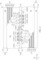
- FIG. 2 is a schematic drawing illustrating a memory device 301 according to a first embodiment of the present disclosure.
- the memory device 301 includes a first substrate 100, a first memory array 110, a second substrate 150, and at least one first vertical transistor T1.
- the first memory array 110 is disposed on the first substrate 100.
- the first memory array 110 includes at least one first word line structure 114.
- the first memory array 110 is disposed between the first substrate 100 and the second substrate 150 in a vertical direction (such as a first direction D1 shown in FIG. 2 ).
- the first vertical transistor T1 is electrically connected with the first word line structure 114. At least a part of the first vertical transistor T1 is disposed in the second substrate 150.
- the area occupied by the first vertical transistor T1 on the second substrate 150 may be relatively smaller than the area occupied by the planar transistor described above, and that will be beneficial to solve the related problems described above.
- the first memory array 110 may include a plurality of the first word line structures 114, and the memory device 301 may include a plurality of the first vertical transistors T1 correspondingly, but not limited thereto.
- the first vertical transistors T1 may be electrically connected with the first word line structures 114 respectively.
- each of the first word line structures 114 may be electrically connected with one of the first vertical transistors T1 in the second substrate 150.
- the first memory array 110 may include an alternating conductive/dielectric stack composed of first dielectric layers 112 and the first word line structures 114 alternately stacked in the first direction D1, and the first memory array 110 may have a first staircase portion P1 at an end of the first memory array 110 in a horizontal direction (such as a second direction D2 shown in FIG. 2 ) for exposing a part of each of the first word line structures 114, but not limited thereto.
- the first direction D1 may be regarded as a thickness direction of the first substrate 100 and/or the first direction D1 may be parallel to the normal direction of a surface of the first substrate 100, and the horizontal direction may be parallel to the surface of the first substrate 100, but not limited thereto.
- the memory device 301 may further include a plurality of first word line contact structures 122.
- Each of the first word line contact structures 122 may be disposed between one of the first vertical transistors T1 and one of the first word line structures 114 in the first direction D1 for electrically connecting the first vertical transistor T1 and the first word line structure 114.
- each of the first word line structures 114 may be electrically connected with one of the first vertical transistors T1 via one of the first word line contact structures 122.
- each of the first vertical transistors T1 may be located corresponding to the exposed part of the corresponding first word line structure 114 in the first direction D1 because the area occupied by the first vertical transistor T1 on the second substrate 150 is relatively smaller, and a connection structure between the first word line structure 114 and the first vertical transistor T1 may be simplified accordingly.
- each of the first word line contact structures 122 may be a pillar structure elongated in the first direction D1, one end of each of the first word line contact structures 122 in the first direction D1 (such as a bottom end of the first word line contact structure 122) may directly contact the exposed part of the corresponding first word line structure 114, and another end of the first word line contact structures 122 in the first direction D1 (such as a top end of the first word line contact structure 122) may directly contact the corresponding first vertical transistor T1, but not limited thereto.
- each of the first vertical transistors T1 may completely cover the corresponding first word line contact structure 122 in the first direction D1, but not limited thereto.
- each of the first vertical transistors T1 may include a first semiconductor channel CH1, a first gate dielectric layer L1, and a first gate electrode G1.
- the first semiconductor channel CH1 may penetrate the second substrate 150 in the first direction D1
- the first gate electrode G1 may be disposed in the second substrate 150 and surround the first semiconductor channel CH1 in a horizontal direction (such as the second direction D2)
- the first gate dielectric layer L1 may be disposed in the second substrate 150 and disposed between the first gate electrode G1 and the first semiconductor channel CH1, but not limited thereto.
- the first semiconductor channel CH1 may be elongated in the first direction D1, but not limited thereto.
- a plurality of first holes H1 may penetrate the second substrate 150 in the first direction D1 respectively, and the first semiconductor channel CH1 and the first gate dielectric layer L1 of the same first vertical transistor T1 may be disposed in one of the first holes H1.
- the second substrate 150 may include a semiconductor substrate, and each of the first gate electrodes G1 may include a first doped region DR1 disposed in the second substrate 150.
- the first holes H1 may penetrate the first doped regions DR1 in the first direction D1, and the first doped regions DR1 may be physically connected with one another, but not limited thereto.
- the first gate electrodes G1 of the first vertical transistors T1 may be physically and electrically connected with one another in the second substrate 150.
- the first gate electrodes G1 may be electrically insulated from one another by isolation structures disposed in the second substrate 150.
- each of the first vertical transistors T1 may be regarded as a surrounding gate transistor, but not limited thereto.
- the first gate electrodes G1 may be formed by implanting suitable dopants into the second substrate 150, and the second substrate 150 may include a semiconductor region (not shown in FIG. 2 ) without being doped by the dopants used to form the first gate electrodes G1, but not limited thereto. It is worth noting that the first vertical transistors T1 of the present disclosure is not limited to the structure described above and other suitable types of vertical transistors may also be used in the present disclosure.
- the first substrate 100 may have a first side S11 and a second side S12 opposite to the first side S11 in the first direction D1
- the second substrate 150 may have a first side S21 and a second side S22 opposite to the first side S21 in the first direction D1.
- the first memory array 110 may be disposed on the first substrate 100
- the first memory array and the first word line contact structures 122 may be disposed at the second side S12 of the first substrate 100 and disposed at the first side S21 of the second substrate 150.
- the first semiconductor channel CH1 of each of the first vertical transistors T1 may penetrate the second substrate 150 in the first direction D1 from the first side S21 of the second substrate 150 to the second side S22 of the second substrate 150, but not limited thereto.
- the memory device 301 may further include a plurality of first conductive lines GW1 and a plurality of first connection structures CS1.
- the first conductive lines GW1 and the first connection structures CS1 may be disposed at the second side S22 of the second substrate 150, and the first connection structures CS1 may be disposed between the first conductive lines GW1 and the second substrate 150 in the first direction D1.
- Each of the first conductive lines GW1 may be electrically connected with one of the first word line structures 114 via one of the first connection structures CS1, one of the first vertical transistors T1, and one of the first word line contact structures 122.
- the first conductive lines GW1 may be regarded as a global word line routing for the first memory array 110, and the first vertical transistors T1 may be regarded as pass gate transistors (or transmission gate transistors) for controlling signals transmitted from the first conductive lines GW1 to the first word line structures 114, but not limited thereto.
- two doped regions may be disposed at two opposite ends of the first semiconductor channel CH1 in the first direction D1, the first word line contact structure 122 may contact one of the two doped regions, and the first connection structure CS 1 may contact another one of the two doped regions, but not limited thereto.
- the first word line contact structure 122 and the first connection structure CS1 may contact the corresponding first semiconductor channel CH1 respectively, and a portion of the first word line contact structure 122 and a portion of the first connection structure CS1 may be regarded as source/drain electrodes of the corresponding first vertical transistor T1, but not limited thereto.
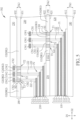
- the memory device 301 may further include a third substrate 200, a second memory array 210, a plurality of second gate contact structures 222, a plurality of second vertical transistors T2, a plurality of second connection structures CS2, and a plurality of second conductive lines GW2.
- the first memory array 110 may be disposed between the first substrate 100 and the third substrate 200 in the first direction D1
- the second substrate 150 is disposed between the first substrate 100 and the third substrate 200 in the first direction D1
- the second memory array 210 and the second gate contact structures 222 may be disposed between the third substrate 200 and the second substrate 150 in the first direction D1
- at least a part of each of the second vertical transistors T2 may be disposed in the second substrate 150, but not limited thereto.
- the third substrate 200 may have a first side S31 and a second side S32 opposite to the first side S31 in the first direction D1, and the second memory array 210 and the second gate contact structures 222 may be disposed on the third substrate 200 and disposed at the first side S31 of the third substrate 200.
- the second memory array 210 may include a plurality of second word line structures 214, the second vertical transistors T2 may be electrically connected with the second word line structures 214 respectively. In other words, each of the second word line structures 214 may be electrically connected with one of the second vertical transistors T2 in the second substrate 150.
- the second memory array 210 may include an alternating conductive/dielectric stack composed of second dielectric layers 212 and the second word line structures 214 alternately stacked in the first direction D1, and the second memory array 210 may have a second staircase portion P2 at an end of the second memory array 210 in a horizontal direction (such as the second direction D2) for exposing a part of each of the second word line structures 214, but not limited thereto.
- each of the second word line contact structures 222 may be disposed between one of the second vertical transistors T2 and one of the second word line structures 214 in the first direction D1 for electrically connecting the second vertical transistor T2 and the second word line structure 214.
- each of the second word line structures 214 may be electrically connected with one of the second vertical transistors T2 via one of the second word line contact structures 222.
- each of the second vertical transistors T2 may include a second semiconductor channel CH2, a second gate dielectric layer L2, and a second gate electrode G2.
- the second semiconductor channel CH2 may penetrate the second substrate 150 in the first direction D1
- the second gate electrode G2 may be disposed in the second substrate 150 and surround the second semiconductor channel CH2 in a horizontal direction (such as the second direction D2)
- the second gate dielectric layer L2 may be disposed in the second substrate 150 and disposed between the second gate electrode G2 and the second semiconductor channel CH2, but not limited thereto.
- the second semiconductor channel CH2 may be elongated in the first direction D1, but not limited thereto.
- a plurality of second holes H2 may penetrate the second substrate 150 in the first direction D1 respectively, and the second semiconductor channel CH2 and the second gate dielectric layer L2 of the same second vertical transistor T2 may be disposed in one of the second holes H2.
- each of the second gate electrodes G2 may include a second doped region DR2 disposed in the second substrate 150, the second holes H2 may penetrate the second doped regions DR2 in the first direction D1, and the second doped regions DR2 may be physically connected with one another, but not limited thereto.
- the second gate electrodes G2 of the second vertical transistors T2 may be physically and electrically connected with one another in the second substrate 150, but not limited thereto.
- the second gate electrodes G2 may be electrically insulated from one another by isolation structures disposed in the second substrate 150.
- each of the second vertical transistors T2 may be regarded as a surrounding gate transistor, but not limited thereto. It is worth noting that the second vertical transistors T2 of the present disclosure is not limited to the structure described above and other suitable types of vertical transistors may also be used in the present disclosure.
- a vertical transistor including a semiconductor channel extending in the vertical direction without penetrating the substrate, a gate electrode surrounding the semiconductor channel in the horizontal direction, and a connection structure penetrating a part of the substrate located under or above the semiconductor channel in the vertical direction for contacting the semiconductor channel may also be used as the first vertical transistor and/or the second vertical transistor in the present disclosure.
- the second gate electrodes G2 may be formed by implanting suitable dopants into the second substrate 150, and the composition of the second doped region DR2 may be similar to the composition of the first doped region DR1, but not limited thereto.
- the structure of the second vertical transistor T2 may be similar to the structure of the first vertical transistor T1 for process simplification, especially when the first vertical transistors T1 and the second vertical transistors T2 are disposed in the same substrate, but not limited thereto.
- the structure of the second vertical transistor T2 may be different from the structure of the first vertical transistor T1 no matter where the first vertical transistors T1 and the second vertical transistors T2 are disposed.
- the second conductive lines GW2 and the second connection structures CS2 may be disposed at the first side S21 of the second substrate 150 and disposed between the second substrate 150 and the first substrate 100 in the first direction D1.
- the second connection structures CS2 may be disposed between the second conductive lines GW2 and the second substrate 150 in the first direction D1.
- Each of the second conductive lines GW2 may be electrically connected with one of the second word line structures 214 via one of the second connection structures CS2, one of the second vertical transistors T2, and one of the second word line contact structures 222.
- the second conductive lines GW2 may be regarded as a global word line routing for the second memory array 210, and the second vertical transistors T2 may be regarded as pass gate transistors (or transmission gate transistors) for controlling signals transmitted from the second conductive lines GW2 to the second word line structures 214, but not limited thereto.
- two doped regions may be disposed at two opposite ends of the second semiconductor channel CH2 in the first direction D1, the second word line contact structure 222 may contact one of the two doped regions, and the second connection structure CS2 may contact another one of the two doped regions, but not limited thereto.
- the second word line contact structure 222 and the second connection structure CS2 may contact the corresponding second semiconductor channel CH2 respectively, and a portion of the second word line contact structure 222 and a portion of the second connection structure CS2 may be regarded as source/drain electrodes of the corresponding second vertical transistor T2, but not limited thereto.
- each of the second vertical transistors T2 may be located corresponding to the exposed part of the corresponding second word line structure 214 in the first direction D1 because the area occupied by the second vertical transistor T2 on the second substrate 150 is relatively smaller, and the second word line contact structure 222 disposed between the second word line structure 214 and the second vertical transistor T2 may be simplified accordingly.
- each of the second word line contact structures 222 may be a pillar structure elongated in the first direction D1, one end of each of the second word line contact structures 222 in the first direction D1 may directly contact the exposed part of the corresponding second word line structure 214, and another end of the second word line contact structures 222 in the first direction D1 may directly contact the corresponding second vertical transistor T2, but not limited thereto.
- each of the second vertical transistors T2 may completely cover the corresponding second word line contact structure 222 in the first direction D1, but not limited thereto.
- the memory device 301 may further include a first isolation structure 152 disposed in the second substrate 150, and at least a part of the isolation structure 152 may be disposed between the first gate electrode G1 of the first vertical transistor T1 and the second gate electrode G2 of the second vertical transistor T2.
- the first gate electrode G1 may be electrically separated from the second gate electrode G2 by the first isolation structure 152, but not limited thereto.
- the first gate electrodes G1 and the second gate electrodes G2 may be disposed in the second substrate 150 and physically and electrically connected with one another.
- the memory device 301 may further include a first interlayer dielectric 120 and a second interlayer dielectric 220.
- the first interlayer dielectric 120 may be disposed between the first substrate 100 and the second substrate 150 and cover the first memory array 110, and the second interlayer dielectric 220 may be disposed between the third substrate 200 and the second substrate 150 and cover the second memory array 210.
- the first word line contact structures 122, the second connection structures CS2, and the second conductive lines GW2 may be disposed in the first interlayer dielectric 120.
- the second word line contact structures 222, the first connection structures CS 1, and the first conductive lines GW1 may be disposed in the second interlayer dielectric 220.
- the first substrate 100, the second substrate 150, and the third substrate 200 may respectively include a semiconductor substrate, such as a silicon substrate, a silicon germanium (SiGe) substrate, a silicon carbide (SiC) substrate, a silicon on insulator (SOI) substrate, a germanium on insulator (GOI) substrate, or other suitable semiconductor substrates or non-semiconductor substrates.
- the second substrate 150 may be relatively thinner for forming the first vertical transistors T1 and/or the second vertical transistors T2, but not limited thereto.
- a thickness TK2 of the second substrate 150 may be less than a thickness TK1 of the first substrate 100 and a thickness TK3 of the third substrate 200.
- the first dielectric layers 112 and the second dielectric layers 212 may include silicon oxide, silicon nitride, silicon oxynitride or other suitable dielectric materials.
- the first word line structures 114, the second word line structures 214, the first word line contact structures 122, the second word line contact structures 222, the first connection structures CS1, the second connection structures CS2, the first conductive lines GW1, and the second conductive lines GW2 may respectively include a low resistivity material and a barrier layer surrounding the low resistivity material, but not limited thereto.
- the low resistivity material mentioned above may include materials having relatively lower resistivity, such as copper, aluminum, cobalt, and tungsten
- the barrier layer mentioned above may include titanium nitride, tantalum nitride, or other suitable barrier materials.
- the first gate dielectric layers L1 and the second gate dielectric layers L2 may include silicon oxide, silicon oxynitride, a high dielectric constant (high-k) dielectric material, or other suitable dielectric materials.
- the first semiconductor channels CH1 and the second semiconductor channels CH2 may include amorphous silicon, polysilicon, or other suitable semiconductor materials.
- the first doped regions DR1 and the second doped regions DR2 may include n-type doped silicon or other suitable doped regions formed in a semiconductor substrate for enhancing electrical conductivity of the first gate electrodes G1 and the second gate electrodes G2.
- the first interlayer dielectric 120 and the second interlayer dielectric 220 may respectively include a plurality of dielectric layers stacked in the first direction D1, and materials of the dielectric layers may include silicon oxide, silicon nitride, silicon oxynitride, low dielectric constant (lowk) dielectric material, any suitable combination thereof, or other suitable dielectric materials.
- the first isolation structure 152 may include a single layer or multiple layers of insulation materials, such as silicon oxide, silicon nitride, silicon oxynitride, or other suitable insulation materials.
- a manufacturing method of the memory device 301 may include but is not limited to the following steps. Firstly, the first memory array 110, the first interlayer dielectric 120, the first word line contact structures 122, the second conductive lines GW2, and the second connection structures CS2 may be formed on the first substrate 100; the second memory array 210, the second interlayer dielectric 220, the second word line contact structures 222, the first conductive lines GW1, and the first connection structures CS1 may be formed on the third substrate 200; and the first vertical transistors T1, the second vertical transistors T2, and the first isolation structure 152 may be formed in the second substrate 150.
- the first substrate 100 with the first memory array 110, the first interlayer dielectric 120, the first word line contact structures 122, the second conductive lines GW2, and the second connection structures CS2 formed thereon, the third substrate 200 with the second memory array 210, the second interlayer dielectric 220, the second word line contact structures 222, the first conductive lines GW1, and the first connection structures CS1 formed thereon, and the second substrate 150 with the first vertical transistors T1 and the second vertical transistors T2 formed therein may be combined with one another by a direct bonding method, such as a metal/dielectric hybrid bonding method, or other suitable bonding approaches.
- a thinning process may be performed to the second substrate 150 before the bonding process for reducing the thickness TK2 of the second substrate 150 and exposing the first vertical transistors T1 and the second vertical transistors T2 at the first side S21 and the second side S22 of the second substrate 150, but not limited thereto.
- other thinning processes may be performed to the first substrate 100 and/or the third substrate 200 before or after the bonding process described above for reducing the total thickness of the memory device 301.
- two or more than two memory arrays disposed on different substrates maybe integrated by the method described above for increasing the total storage capacity of the memory device and simplifying the related routing design.
- the memory array described above may include a 3D NAND memory array, a 3D NOR memory array, a dynamic random access memory (DRAM) array, a 3D XPoint memory array, or other suitable 3D memory structures.
- memory strings (not shown) may penetrate the alternating conductive/dielectric stack of the memory array in the first direction D1.
- Each of the memory strings may have a cylinder shape (e.g., a pillar shape) elongated in the first direction D1, and each of the memory strings may include a channel layer, a tunneling layer, a storage layer, and a blocking layer arranged radially from the center toward the outer surface of the pillar in this order, but not limited thereto.
- the memory arrays in the present disclosure are not limited to the structure shown in FIG. 2 and/or the structure described above, and other suitable memory array architectures may also be applied in the present disclosure.
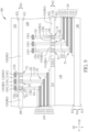
- FIG. 3 is a schematic drawing illustrating a memory device according to an embodiment of the present disclosure
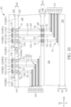
- FIG. 4 is a schematic drawing illustrating a top view of a portion of a memory device according to an embodiment of the present disclosure
- FIG. 3 may be regarded as a schematic drawing illustrating another portion of the memory device 301 in the first embodiment described above
- FIG. 4 may be regarded as a schematic drawing illustrating a top view of a portion of a memory device similar to the memory device 301 in the first embodiment described above, but not limited thereto.
- the memory device 301 may further include a third connection structure CS3 and a third conductive line GC disposed at the second side S22 of the second substrate 150 and disposed in the second interlayer dielectric 220.
- the third conductive line GC may be electrically connected with the first gate electrodes G1 of the first vertical transistors T1 via the third connection structure CS3 for transmitting signals to the first gate electrodes G1 and controlling the switching condition of the first vertical transistors T1.
- the third connection structure CS3 and the first connection structures CS1 may be formed with the same composition and/or be formed by the same process, and the third conductive line GC and the first conductive lines GW1 may be formed with the same composition and/or be formed by the same process, but not limited thereto.
- the second substrate 150 may include a semiconductor region 154, and at least a part of the first isolation structure 152 may be disposed between the semiconductor region 154 and the first gate electrode G1.
- Other circuit structures (not shown) may be formed on and/or formed in the semiconductor region 154, but not limited thereto.
- the first memory array 110 may be divided into memory blocks 110A by a slit structure (not shown), and each of the first conductive lines GW1 may be elongated in another horizontal direction (such as a third direction D3 shown in FIG. 4 ) and overlap the first staircase portions P1 of different memory blocks 110A in the first direction D1.
- the first gate electrodes G1 corresponding to different memory blocks 110A may be separated from one another by the first isolation structure 152, and the third conductive line GC may be elongated in the second direction D2 substantially orthogonal to the third direction D3, but not limited thereto.
- the semiconductor region 154 may be separated from the first gate electrodes G1 by the first isolation structure 152, and the semiconductor region 154 may not overlap the first staircase portions P1 in the first direction D1 accordingly, but not limited thereto. It is worth noting that components similar to the third conductive line GC and the third connection structure CS3 described above may be applied to the second memory array 210 in the present disclosure, and the features shown in FIG. 3 and FIG. 4 may also be applied in other embodiments of the present disclosure.
- FIG. 5 is a schematic drawing illustrating a memory device 302 according to a second embodiment of the present disclosure.
- the second memory array 210 may be disposed on the second substrate 150, a part of the second interlay dielectric 220 may be disposed between the second memory array 210 and the third substrate 200 in the first direction D1, and at least a part of each of the second vertical transistors T2 may be disposed in the third substrate 200.
- the second semiconductor channel CH2 may penetrate the third substrate 200 in the first direction D1
- the second gate electrode G2 may be disposed in the third substrate 200 and surround the second semiconductor channel CH2 in the horizontal direction
- the second gate dielectric layer L2 may be disposed in the third substrate 200 and disposed between the second gate electrode G2 and the second semiconductor channel CH2, but not limited thereto.
- each of the second gate electrodes G2 may include a second doped region DR2 disposed in the third substrate 200, and the second holes H2 may penetrate the second doped regions DR2 in the first direction D1, but not limited thereto.
- the second gate electrodes G2 of the second vertical transistors T2 may be physically and electrically connected with one another in the third substrate 150, and the second gate electrodes G2 of the second vertical transistors T2 may be separated from the first gate electrodes G1 of the first vertical transistors T1.
- the second connection structures CS2 and the second conductive lines GW2 may be disposed at the second side S32 of the third substrate 200 and a protection layer 230 may be disposed on the third substrate 200 and cover the second connection structures CS2 and the second conductive lines GW2.
- the protection layer 230 may include silicon oxide, silicon nitride, or other suitable insulation materials.
- the second memory array 210 may be disposed on the semiconductor region 154, and a part of the first memory array 110 may overlap the second memory array 210 in the first direction D1, but not limited thereto.
- a manufacturing method of the memory device 302 may include but is not limited to the following steps. Firstly, the first memory array 110, the first interlayer dielectric 120, and the first word line contact structures 122 may be formed on the first substrate 100; the first vertical transistors T1 and the first isolation structure 152 may be formed in the second substrate 150; the second memory array 210, the second interlayer dielectric 220, the second word line contact structures 222, the first conductive lines GW1, and the first connection structures CS1 may be formed on the third substrate 200; the second vertical transistors T2 may be formed in the third substrate 200; and the second conductive lines GW2, the second connection structures CS2; and the protection layer 230 may be formed on the third substrate 200.
- the first substrate 100 with the first memory array 110, the first interlayer dielectric 120, and the first word line contact structures 122 formed thereon, the second substrate 150 with the first vertical transistors T1 formed therein and the second memory array 210, the second interlayer dielectric 220, the second word line contact structures 222, the first conductive lines GW1, and the first connection structures CS1 formed thereon, and the third substrate 200 with the second vertical transistors T2 formed therein and the second conductive lines GW2, the second connection structures CS2, and the protection layer 230 formed thereon may be combined with one another by a direct bonding method, such as a metal/dielectric hybrid bonding method, or other suitable bonding approaches.
- a direct bonding method such as a metal/dielectric hybrid bonding method, or other suitable bonding approaches.
- thinning processes may be performed to the second substrate 150 and/or the third substrate 200 before the bonding process for reducing the thickness TK2 of the second substrate 150 and the thickness TK3 of the third substrate 200, exposing the first vertical transistors T1 at the first side S21 and the second side S22 of the second substrate 150, and exposing the second vertical transistors T2 at the first side S31 and the second side S32 of the third substrate 200, but not limited thereto.
- the thickness TK2 of the second substrate 150 and the thickness TK3 of the third substrate 200 may be less than the thickness of the first substrate 100, but not limited thereto.
- FIG. 6 is a schematic drawing illustrating a memory device 303 according to a third embodiment of the present disclosure.
- the third substrate 200 may be disposed between the first substrate 100 and the second substrate 150 in the first direction D1
- the second memory array 210 may be disposed between the second substrate 150 and the third substrate 200 in the first direction D1.
- the second memory array 210 may be disposed on the third substrate 200 and disposed at the second side S32 of the third substrate 200 and the first side S21 of the second substrate 150, and the first conductive lines GW1, the second conductive lines GW2, the first connection structures CS1, the second connection structures CS2, and the protection layer 230 may be disposed on the second substrate 150 and disposed at the second side S22 of the second substrate 150.
- the memory device 303 may further include a plurality of fourth connection structures CS4, a plurality of through substrate connection structures TS, and a second isolation structure 240.
- the second isolation structure 240 may be disposed in the third substrate 200, each of the through substrate connection structures TS may be disposed in the third substrate 200 and penetrating the second isolation structure 240 in the first direction D1, and each of the fourth connection structures CS4 may be disposed in the second interlayer dielectric 220 and disposed between one of the second vertical transistors T2 and one of the through substrate connection structures TS in the first direction D1.
- Each of the through substrate connection structures TS may be electrically connected with one of the first word line contact structures 122 and one of the fourth connection structures CS4, and each of the fourth connection structures CS4 may be electrically connected with one of the first vertical transistors T1.
- each of the first conductive lines GW1 may be electrically connected with one of the first word line structures 114 via one of the first connection structures CS1, one of the first vertical transistors T1, one of the fourth connection structures CS4, one of the through substrate connection structures TS, and one of the first word line contact structures 122.
- the second isolation structure 240 may include a single layer or multiple layers of insulation materials, such as silicon oxide, silicon nitride, silicon oxynitride, or other suitable insulation materials.
- the fourth connection structures CS4 and the through substrate connection structures TS may include a low resistivity material and a barrier layer surrounding the low resistivity material, but not limited thereto.
- the low resistivity material mentioned above may include materials having relatively lower resistivity, such as copper, aluminum, cobalt, and tungsten
- the barrier layer mentioned above may include titanium nitride, tantalum nitride, or other suitable barrier materials.
- a manufacturing method of the memory device 303 may include but is not limited to the following steps. Firstly, the first memory array 110, the first interlayer dielectric 120, and the first word line contact structures 122 may be formed on the first substrate 100; the through substrate connection structures TS and the second isolation structure 240 may be formed in the third substrate 200; the second memory array 210, the second interlayer dielectric 220, the second word line contact structures 222, and the fourth connection structures CS4 may be formed on the third substrate 200; the first vertical transistors T1, the second vertical transistors T2, and the first isolation structure 152 may be formed in the second substrate 150; and the first connection structures CS1, the second connection structures CS2, the first conductive lines GW1, the second conductive lines GW2, and the protection layer 230 may be formed on the second substrate 150.
- the first substrate 100 with the first memory array 110, the first interlayer dielectric 120, and the first word line contact structures 122 formed thereon, the third substrate 200 with the through substrate connection structures TS and the second isolation structure 240 formed therein and the second memory array 210, the second interlayer dielectric 220, the second word line contact structures 222, and the fourth connection structures CS4 formed thereon, and the second substrate 150 with the first vertical transistors T1, the second vertical transistors T2, and the first isolation structure 152 formed therein and the first connection structures CS1, the second connection structures CS2, the first conductive lines GW1, the second conductive lines GW2, and the protection layer 230 formed thereon may be combined with one another by a direct bonding method, such as a metal/dielectric hybrid bonding method, or other suitable bonding approaches.
- a direct bonding method such as a metal/dielectric hybrid bonding method, or other suitable bonding approaches.
- a thinning process may be performed to the second substrate 150 before the bonding process for reducing the thickness TK2 of the second substrate 150 and exposing the first vertical transistors T1 and the second vertical transistors T2 at the first side S21 and the second side S22 of the second substrate 150, but not limited thereto.
- FIG. 7 is a schematic drawing illustrating a memory device 304 according to a fourth embodiment of the present disclosure.
- the first conductive lines GW1, the second conductive lines GW2, the first connection structures CS1, the second connection structures CS2, and the protection layer 230 may be disposed on the third substrate 200 and disposed at the second side S32 of the third substrate 200.
- the second isolation structure 240 and the through substrate connection structures TS may be disposed in the third substrate 200, and each of the first vertical transistors T1 in the second substrate 150 may be electrically connected with one of the first conductive lines GW1 via one the fourth connection structures CS4, one of the through substrate connection structures TS, and one of the first connection structures CS1.
- FIG. 8 is a schematic drawing illustrating a memory device 305 according to a fifth embodiment of the present disclosure.
- the first gate electrodes G1 of the first vertical transistors T1 may be physically and electrically connected with the second gate electrodes G2 of the second vertical transistors T2.
- the first gate electrodes G1 and the second gate electrodes G2 may be formed with the same doped region (such as the first doped region DR1) in the second substrate 150, but not limited thereto.
- FIG. 9 is a schematic drawing illustrating a memory device 306 according to a sixth embodiment of the present disclosure.
- the difference between the memory device 306 in this embodiment and the memory device 302 described above is that, in the memory device 306, the second memory array 210 may not overlap the first memory array 110 in the first direction D1, and in a top view of the memory device 306, the second staircase portion P2 of the second memory array 210 may be disposed adjacent to the first staircase portion P1 in the second direction D2, but not limited thereto.
- the shape of the second memory array 210 may be the same as a mirror image of the shape of the first memory array 110, and the shape of the first memory array 110 and the shape of the second memory array 210 may be a mirror symmetry patterns in some embodiments, but not limited thereto. It is worth noting that the relative allocation of the first memory array 110 and the second memory array 210 may also be applied in other embodiments of the present disclosure.
- FIG. 10 is a schematic drawing illustrating a memory device 307 according to a seventh embodiment of the present disclosure.
- the difference between the memory device 307 in this embodiment and the memory device 303 described above is that, in the memory device 307, the second memory array 210 may not overlap the first memory array 110 in the first direction D1, and in a top view of the memory device 307, the second staircase portion P2 of the second memory array 210 may be disposed adjacent to the first staircase portion P1 in the second direction D2, but not limited thereto.
- the shape of the second memory array 210 may be the same as a mirror image of the shape of the first memory array 110, and the shape of the first memory array 110 and the shape of the second memory array 210 may be a mirror symmetry patterns in some embodiments, but not limited thereto.
- the vertical transistors disposed in the substrate are electrically connected to the word line structures of the memory array disposed on another substrate respectively.
- the area occupied by the vertical transistors on the substrate may be reduced, and the word line contact structures located between the vertical transistors and the word line structures may be simplified accordingly.
Abstract
A memory device includes a first substrate, a first memory array, a second substrate, and at least one first vertical transistor. The first memory array is disposed on the first substrate. The first memory array includes at least one first word line structure. The first memory array is disposed between the first substrate and the second substrate in a vertical direction. The first vertical transistor is electrically connected with the first word line structure. At least a part of the at least one first vertical transistor is disposed in the second substrate.
Description
- The present disclosure relates to a memory device, and more particularly, to a memory device including a vertical transistor.
- Planar memory cells are scaled to smaller sizes by improving process technology, circuit design, programming algorithm, and fabrication process. However, as feature sizes of the memory cells approach a lower limit, planar process and fabrication techniques become challenging and costly. As a result, memory density for planar memory cells approaches an upper limit.
- A three-dimensional (3D) memory architecture can address the density limitation in planar memory cells. The 3D memory architecture includes a memory array and peripheral devices for controlling signals to and from the memory array. As the dimension of the memory device becomes smaller and the memory cell density becomes higher, the interconnection structure between the memory array and the peripheral devices becomes more complicated and influences the related circuit design and/or the related manufacturing processes.
- A memory device is provided in the present disclosure. In the memory device, a vertical transistor disposed in a substrate is electrically connected to a word line structure of a memory array disposed on another substrate. An area occupied by the vertical transistor on the substrate may be reduced, and a connection structure between the vertical transistor and the word line structure may be simplified accordingly.
- According to an embodiment of the present disclosure, a memory device is provided. The memory device includes a first substrate, a first memory array, a second substrate, and at least one first vertical transistor. The first memory array is disposed on the first substrate. The first memory array includes at least one first word line structure. The first memory array is disposed between the first substrate and the second substrate in a vertical direction. The first vertical transistor is electrically connected with the first word line structure. At least a part of the at least one first vertical transistor is disposed in the second substrate.
- In some embodiments, the at least one first vertical transistor includes a first semiconductor channel penetrating the second substrate in the vertical direction.
- In some embodiments, the at least one first vertical transistor further includes a first gate electrode disposed in the second substrate and surrounding the first semiconductor channel in a horizontal direction.
- In some embodiments, the at least one first vertical transistor further includes a first gate dielectric layer disposed in the second substrate and disposed between the first gate electrode and the first semiconductor channel.
- In some embodiments, the first memory array includes a plurality of the at least one first word line structures, and the memory device comprises a plurality of the at least one first vertical transistors electrically connected with the plurality of the at least one first word line structures respectively.
- In some embodiments, the first gate electrodes of the plurality of the at least one first vertical transistors are physically and electrically connected with one another in the second substrate.
- In some embodiments, the second substrate includes a semiconductor region, and the first gate electrode includes a doped region disposed in the second substrate.
- In some embodiments, the memory device further includes an isolation structure disposed in the second substrate, and the isolation structure is disposed between the semiconductor region and the first gate electrode.
- In some embodiments, the memory device further includes a word line contact structure disposed between the at least one first vertical transistor and the at least one first word line structure, and the at least one first word line structure is electrically connected with the at least one first vertical transistor via the word line contact structure.
- In some embodiments, the at least one first vertical transistor completely covers the word line contact structure in the vertical direction.
- In some embodiments, the second substrate has a first side and a second side opposite to the first side in the vertical direction, and the first memory array and the word line contact structure are disposed at the first side of the second substrate.
- In some embodiments, the memory device further includes a conductive line and a connection structure. The conductive line is disposed at the second side of the second substrate, and the connection structure is disposed at the second side of the second substrate and disposed between the conductive line and the at least one first vertical transistor. The conductive line is electrically connected with the at least one first word line structure via the connection structure, the at least one first vertical transistor, and the word line contact structure.
- In some embodiments, the memory device further includes a third substrate, a second memory array, and at least one second vertical transistor. The first memory array is disposed between the first substrate and the third substrate in the vertical direction. The second memory array includes at least one second word line structure. The at least one second vertical transistor is electrically connected with the at least one second word line structure.
- In some embodiments, the second memory array is disposed on the third substrate, and at least a part of the at least one second vertical transistor is disposed in the second substrate.
- In some embodiments, the at least one second vertical transistor includes a second semiconductor channel and a second gate electrode. The second semiconductor channel penetrates the second substrate in the vertical direction. The second gate electrode is disposed in the second substrate and surrounds the second semiconductor channel in a horizontal direction.
- In some embodiments, the at least one first vertical transistor includes a first gate electrode disposed in the second substrate, and the first gate electrode is physically and electrically connected with the second gate electrode.
- In some embodiments, the at least one first vertical transistor includes a first gate electrode disposed in the second substrate, and the first gate electrode is electrically separated from the second gate electrode.
- In some embodiments, the third substrate is disposed between the first substrate and the second substrate in the vertical direction, and the second memory array is disposed between the second substrate and the third substrate in the vertical direction.
- In some embodiments, the second substrate is disposed between the first substrate and the third substrate in the vertical direction, and the second memory array is disposed between the second substrate and the third substrate in the vertical direction.
- In some embodiments, the second memory array is disposed on the second substrate, and at least a part of the at least one second vertical transistor is disposed in the third substrate.
- Other aspects of the present disclosure can be understood by those skilled in the art in light of the description, the claims, and the drawings of the present disclosure.
- These and other objectives of the present invention will no doubt become obvious to those of ordinary skill in the art after reading the following detailed description of the preferred embodiment that is illustrated in the various figures and drawings.
- The accompanying drawings, which are incorporated herein and form a part of the specification, illustrate embodiments of the present disclosure and, together with the description, further serve to explain the principles of the present disclosure and to enable a person skilled in the pertinent art to make and use the present disclosure.
-
FIG. 1 is a schematic drawing illustrating a memory device according to an embodiment of the present disclosure. -
FIG. 2 is a schematic drawing illustrating a memory device according to a first embodiment of the present disclosure. -
FIG. 3 is a schematic drawing illustrating a memory device according to an embodiment of the present disclosure. -
FIG. 4 is a schematic drawing illustrating a top view of a portion of a memory device according to an embodiment of the present disclosure. -
FIG. 5 is a schematic drawing illustrating a memory device according to a second embodiment of the present disclosure. -
FIG. 6 is a schematic drawing illustrating a memory device according to a third embodiment of the present disclosure. -
FIG. 7 is a schematic drawing illustrating a memory device according to a fourth embodiment of the present disclosure. -
FIG. 8 is a schematic drawing illustrating a memory device according to a fifth embodiment of the present disclosure. -
FIG. 9 is a schematic drawing illustrating a memory device according to a sixth embodiment of the present disclosure. -
FIG. 10 is a schematic drawing illustrating a memory device according to a seventh embodiment of the present disclosure. - Although specific configurations and arrangements are discussed, it should be understood that this is done for illustrative purposes only. A person skilled in the pertinent art will recognize that other configurations and arrangements can be used without departing from the spirit and scope of the present disclosure. It will be apparent to a person skilled in the pertinent art that the present disclosure can also be employed in a variety of other applications.
- It is noted that references in the specification to "one embodiment," "an embodiment," "some embodiments," etc., indicate that the embodiment described may include a particular feature, structure, or characteristic, but every embodiment may not necessarily include the particular feature, structure, or characteristic. Moreover, such phrases do not necessarily refer to the same embodiment. Further, when a particular feature, structure or characteristic is described in connection with an embodiment, it would be within the knowledge of a person skilled in the pertinent art to effect such feature, structure or characteristic in connection with other embodiments whether or not explicitly described.
- In general, terminology may be understood at least in part from usage in context. For example, the term "one or more" as used herein, depending at least in part upon context, may be used to describe any feature, structure, or characteristic in a singular sense or may be used to describe combinations of features, structures or characteristics in a plural sense. Similarly, terms, such as "a," "an," or "the," again, may be understood to convey a singular usage or to convey a plural usage, depending at least in part upon context. In addition, the term "based on" may be understood as not necessarily intended to convey an exclusive set of factors and may, instead, allow for existence of additional factors not necessarily expressly described, again, depending at least in part on context.
- It will be understood that, although the terms first, second, etc. may be used herein to describe various elements, components, regions, layers and/or sections, these elements, components, regions, layers and/or sections should not be limited by these terms. These terms are only used to distinguish one element, component, region, layer and/or section from another. Thus, a first element, component, region, layer or section discussed below could be termed a second element, component, region, layer or section without departing from the teachings of the disclosure.
- It should be readily understood that the meaning of "on," "above," and "over" in the present disclosure should be interpreted in the broadest manner such that "on" not only means "directly on" something but also includes the meaning of "on" something with an intermediate feature or a layer therebetween, and that "above" or "over" not only means the meaning of "above" or "over" something but can also include the meaning it is "above" or "over" something with no intermediate feature or layer therebetween (i.e., directly on something).
- Further, spatially relative terms, such as "beneath," "below," "lower," "above," "upper," and the like, may be used herein for ease of description to describe one element or feature's relationship to another element(s) or feature(s) as illustrated in the figures. The spatially relative terms are intended to encompass different orientations of the device in use or operation in addition to the orientation depicted in the figures. The apparatus may be otherwise oriented (rotated 90 degrees or at other orientations) and the spatially relative descriptors used herein may likewise be interpreted accordingly.
- The term "forming" or the term "disposing" are used hereinafter to describe the behavior of applying a layer of material to an object. Such terms are intended to describe any possible layer forming techniques including, but not limited to, thermal growth, sputtering, evaporation, chemical vapor deposition, epitaxial growth, electroplating, and the like.
- Please refer to
FIG. 1. FIG. 1 is a schematic drawing illustrating a memory device according to an embodiment of the present disclosure. As shown inFIG. 1 , in the memory device, anNAND memory array 920 may be disposed on asubstrate 910, andplanar transistors 950 configured to be electrically connected with theNAND memory array 920 may be disposed on anothersubstrate 940. TheNAND memory array 920 may include an alternating conductive/dielectric stack composed ofdielectric layers 922 andconductive layers 924 alternately stacked in a vertical direction (such as a first direction D1 shown inFIG. 1 ), and each of theconductive layers 924 may be regarded as a word line in theNAND memory array 920. The alternating conductive/dielectric stack may have a staircase portion exposing a part of each word line, and each of the word lines may be electrically connected to a corresponding driving unit accordingly. For example, each of theplanar transistors 950 may be electrically connected to one of the word lines via aninterconnection structure 930 for controlling signals transmitting to the word lines, and theplanar transistors 950 may be regarded as the driving units described above, but not limited thereto. However, each of theplanar transistors 950 occupies a specific area on thesubstrate 940, most of theplanar transistors 950 cannot be located corresponding to the exposed parts of the word lines exactly in the first direction D1, and theinterconnection structure 930 has to become complicated accordingly. Additionally, the tiers of the word lines will be limited to a specific range because of the total area occupied by theplanar transistors 950 on thesubstrate 940, and the storage capacity of the memory device is limited accordingly. - Please refer to
FIG. 2. FIG. 2 is a schematic drawing illustrating amemory device 301 according to a first embodiment of the present disclosure. As shown inFIG. 2 , thememory device 301 includes afirst substrate 100, afirst memory array 110, asecond substrate 150, and at least one first vertical transistor T1. Thefirst memory array 110 is disposed on thefirst substrate 100. Thefirst memory array 110 includes at least one firstword line structure 114. Thefirst memory array 110 is disposed between thefirst substrate 100 and thesecond substrate 150 in a vertical direction (such as a first direction D1 shown inFIG. 2 ). The first vertical transistor T1 is electrically connected with the firstword line structure 114. At least a part of the first vertical transistor T1 is disposed in thesecond substrate 150. The area occupied by the first vertical transistor T1 on thesecond substrate 150 may be relatively smaller than the area occupied by the planar transistor described above, and that will be beneficial to solve the related problems described above. - In some embodiments, the
first memory array 110 may include a plurality of the firstword line structures 114, and thememory device 301 may include a plurality of the first vertical transistors T1 correspondingly, but not limited thereto. The first vertical transistors T1 may be electrically connected with the firstword line structures 114 respectively. In other words, each of the firstword line structures 114 may be electrically connected with one of the first vertical transistors T1 in thesecond substrate 150. In some embodiments, thefirst memory array 110 may include an alternating conductive/dielectric stack composed of firstdielectric layers 112 and the firstword line structures 114 alternately stacked in the first direction D1, and thefirst memory array 110 may have a first staircase portion P1 at an end of thefirst memory array 110 in a horizontal direction (such as a second direction D2 shown inFIG. 2 ) for exposing a part of each of the firstword line structures 114, but not limited thereto. The first direction D1 may be regarded as a thickness direction of thefirst substrate 100 and/or the first direction D1 may be parallel to the normal direction of a surface of thefirst substrate 100, and the horizontal direction may be parallel to the surface of thefirst substrate 100, but not limited thereto. In some embodiments, thememory device 301 may further include a plurality of first wordline contact structures 122. Each of the first wordline contact structures 122 may be disposed between one of the first vertical transistors T1 and one of the firstword line structures 114 in the first direction D1 for electrically connecting the first vertical transistor T1 and the firstword line structure 114. In other words, each of the firstword line structures 114 may be electrically connected with one of the first vertical transistors T1 via one of the first wordline contact structures 122. - In some embodiments, each of the first vertical transistors T1 may be located corresponding to the exposed part of the corresponding first
word line structure 114 in the first direction D1 because the area occupied by the first vertical transistor T1 on thesecond substrate 150 is relatively smaller, and a connection structure between the firstword line structure 114 and the first vertical transistor T1 may be simplified accordingly. For example, in some embodiments, each of the first wordline contact structures 122 may be a pillar structure elongated in the first direction D1, one end of each of the first wordline contact structures 122 in the first direction D1 (such as a bottom end of the first word line contact structure 122) may directly contact the exposed part of the corresponding firstword line structure 114, and another end of the first wordline contact structures 122 in the first direction D1 (such as a top end of the first word line contact structure 122) may directly contact the corresponding first vertical transistor T1, but not limited thereto. In some embodiments, each of the first vertical transistors T1 may completely cover the corresponding first wordline contact structure 122 in the first direction D1, but not limited thereto. - In some embodiments, each of the first vertical transistors T1 may include a first semiconductor channel CH1, a first gate dielectric layer L1, and a first gate electrode G1. The first semiconductor channel CH1 may penetrate the
second substrate 150 in the first direction D1, the first gate electrode G1 may be disposed in thesecond substrate 150 and surround the first semiconductor channel CH1 in a horizontal direction (such as the second direction D2), and the first gate dielectric layer L1 may be disposed in thesecond substrate 150 and disposed between the first gate electrode G1 and the first semiconductor channel CH1, but not limited thereto. In some embodiments, the first semiconductor channel CH1 may be elongated in the first direction D1, but not limited thereto. In some embodiments, a plurality of first holes H1 may penetrate thesecond substrate 150 in the first direction D1 respectively, and the first semiconductor channel CH1 and the first gate dielectric layer L1 of the same first vertical transistor T1 may be disposed in one of the first holes H1. Additionally, thesecond substrate 150 may include a semiconductor substrate, and each of the first gate electrodes G1 may include a first doped region DR1 disposed in thesecond substrate 150. In some embodiments, the first holes H1 may penetrate the first doped regions DR1 in the first direction D1, and the first doped regions DR1 may be physically connected with one another, but not limited thereto. In other words, the first gate electrodes G1 of the first vertical transistors T1 may be physically and electrically connected with one another in thesecond substrate 150. However, in some embodiments, the first gate electrodes G1 may be electrically insulated from one another by isolation structures disposed in thesecond substrate 150. In some embodiments, each of the first vertical transistors T1 may be regarded as a surrounding gate transistor, but not limited thereto. In some embodiments, the first gate electrodes G1 may be formed by implanting suitable dopants into thesecond substrate 150, and thesecond substrate 150 may include a semiconductor region (not shown inFIG. 2 ) without being doped by the dopants used to form the first gate electrodes G1, but not limited thereto. It is worth noting that the first vertical transistors T1 of the present disclosure is not limited to the structure described above and other suitable types of vertical transistors may also be used in the present disclosure. - In some embodiments, the
first substrate 100 may have a first side S11 and a second side S12 opposite to the first side S11 in the first direction D1, and thesecond substrate 150 may have a first side S21 and a second side S22 opposite to the first side S21 in the first direction D1. Thefirst memory array 110 may be disposed on thefirst substrate 100, and the first memory array and the first wordline contact structures 122 may be disposed at the second side S12 of thefirst substrate 100 and disposed at the first side S21 of thesecond substrate 150. The first semiconductor channel CH1 of each of the first vertical transistors T1 may penetrate thesecond substrate 150 in the first direction D1 from the first side S21 of thesecond substrate 150 to the second side S22 of thesecond substrate 150, but not limited thereto. In some embodiments, thememory device 301 may further include a plurality of first conductive lines GW1 and a plurality of first connection structures CS1. The first conductive lines GW1 and the first connection structures CS1 may be disposed at the second side S22 of thesecond substrate 150, and the first connection structures CS1 may be disposed between the first conductive lines GW1 and thesecond substrate 150 in the first direction D1. Each of the first conductive lines GW1 may be electrically connected with one of the firstword line structures 114 via one of the first connection structures CS1, one of the first vertical transistors T1, and one of the first wordline contact structures 122. - In some embodiments, the first conductive lines GW1 may be regarded as a global word line routing for the
first memory array 110, and the first vertical transistors T1 may be regarded as pass gate transistors (or transmission gate transistors) for controlling signals transmitted from the first conductive lines GW1 to the firstword line structures 114, but not limited thereto. In some embodiments, two doped regions (not shown) may be disposed at two opposite ends of the first semiconductor channel CH1 in the first direction D1, the first wordline contact structure 122 may contact one of the two doped regions, and the first connection structure CS 1 may contact another one of the two doped regions, but not limited thereto. In some embodiments, the first wordline contact structure 122 and the first connection structure CS1 may contact the corresponding first semiconductor channel CH1 respectively, and a portion of the first wordline contact structure 122 and a portion of the first connection structure CS1 may be regarded as source/drain electrodes of the corresponding first vertical transistor T1, but not limited thereto. - In some embodiments, the
memory device 301 may further include athird substrate 200, asecond memory array 210, a plurality of secondgate contact structures 222, a plurality of second vertical transistors T2, a plurality of second connection structures CS2, and a plurality of second conductive lines GW2. Thefirst memory array 110 may be disposed between thefirst substrate 100 and thethird substrate 200 in the first direction D1, thesecond substrate 150 is disposed between thefirst substrate 100 and thethird substrate 200 in the first direction D1, thesecond memory array 210 and the secondgate contact structures 222 may be disposed between thethird substrate 200 and thesecond substrate 150 in the first direction D1, and at least a part of each of the second vertical transistors T2 may be disposed in thesecond substrate 150, but not limited thereto. In some embodiments, thethird substrate 200 may have a first side S31 and a second side S32 opposite to the first side S31 in the first direction D1, and thesecond memory array 210 and the secondgate contact structures 222 may be disposed on thethird substrate 200 and disposed at the first side S31 of thethird substrate 200. - In some embodiments, the
second memory array 210 may include a plurality of secondword line structures 214, the second vertical transistors T2 may be electrically connected with the secondword line structures 214 respectively. In other words, each of the secondword line structures 214 may be electrically connected with one of the second vertical transistors T2 in thesecond substrate 150. In some embodiments, thesecond memory array 210 may include an alternating conductive/dielectric stack composed of seconddielectric layers 212 and the secondword line structures 214 alternately stacked in the first direction D1, and thesecond memory array 210 may have a second staircase portion P2 at an end of thesecond memory array 210 in a horizontal direction (such as the second direction D2) for exposing a part of each of the secondword line structures 214, but not limited thereto. In some embodiments, each of the second wordline contact structures 222 may be disposed between one of the second vertical transistors T2 and one of the secondword line structures 214 in the first direction D1 for electrically connecting the second vertical transistor T2 and the secondword line structure 214. In other words, each of the secondword line structures 214 may be electrically connected with one of the second vertical transistors T2 via one of the second wordline contact structures 222. - In some embodiments, each of the second vertical transistors T2 may include a second semiconductor channel CH2, a second gate dielectric layer L2, and a second gate electrode G2. In some embodiments, the second semiconductor channel CH2 may penetrate the
second substrate 150 in the first direction D1, the second gate electrode G2 may be disposed in thesecond substrate 150 and surround the second semiconductor channel CH2 in a horizontal direction (such as the second direction D2), and the second gate dielectric layer L2 may be disposed in thesecond substrate 150 and disposed between the second gate electrode G2 and the second semiconductor channel CH2, but not limited thereto. In some embodiments, the second semiconductor channel CH2 may be elongated in the first direction D1, but not limited thereto. In some embodiments, a plurality of second holes H2 may penetrate thesecond substrate 150 in the first direction D1 respectively, and the second semiconductor channel CH2 and the second gate dielectric layer L2 of the same second vertical transistor T2 may be disposed in one of the second holes H2. In some embodiments, each of the second gate electrodes G2 may include a second doped region DR2 disposed in thesecond substrate 150, the second holes H2 may penetrate the second doped regions DR2 in the first direction D1, and the second doped regions DR2 may be physically connected with one another, but not limited thereto. In other words, the second gate electrodes G2 of the second vertical transistors T2 may be physically and electrically connected with one another in thesecond substrate 150, but not limited thereto. In some embodiments, the second gate electrodes G2 may be electrically insulated from one another by isolation structures disposed in thesecond substrate 150. In some embodiments, each of the second vertical transistors T2 may be regarded as a surrounding gate transistor, but not limited thereto. It is worth noting that the second vertical transistors T2 of the present disclosure is not limited to the structure described above and other suitable types of vertical transistors may also be used in the present disclosure. For example, a vertical transistor including a semiconductor channel extending in the vertical direction without penetrating the substrate, a gate electrode surrounding the semiconductor channel in the horizontal direction, and a connection structure penetrating a part of the substrate located under or above the semiconductor channel in the vertical direction for contacting the semiconductor channel may also be used as the first vertical transistor and/or the second vertical transistor in the present disclosure. - In some embodiments, the second gate electrodes G2 may be formed by implanting suitable dopants into the
second substrate 150, and the composition of the second doped region DR2 may be similar to the composition of the first doped region DR1, but not limited thereto. The structure of the second vertical transistor T2 may be similar to the structure of the first vertical transistor T1 for process simplification, especially when the first vertical transistors T1 and the second vertical transistors T2 are disposed in the same substrate, but not limited thereto. In some embodiments, the structure of the second vertical transistor T2 may be different from the structure of the first vertical transistor T1 no matter where the first vertical transistors T1 and the second vertical transistors T2 are disposed. - In some embodiments, the second conductive lines GW2 and the second connection structures CS2 may be disposed at the first side S21 of the
second substrate 150 and disposed between thesecond substrate 150 and thefirst substrate 100 in the first direction D1. The second connection structures CS2 may be disposed between the second conductive lines GW2 and thesecond substrate 150 in the first direction D1. Each of the second conductive lines GW2 may be electrically connected with one of the secondword line structures 214 via one of the second connection structures CS2, one of the second vertical transistors T2, and one of the second wordline contact structures 222. In some embodiments, the second conductive lines GW2 may be regarded as a global word line routing for thesecond memory array 210, and the second vertical transistors T2 may be regarded as pass gate transistors (or transmission gate transistors) for controlling signals transmitted from the second conductive lines GW2 to the secondword line structures 214, but not limited thereto. In some embodiments, two doped regions (not shown) may be disposed at two opposite ends of the second semiconductor channel CH2 in the first direction D1, the second wordline contact structure 222 may contact one of the two doped regions, and the second connection structure CS2 may contact another one of the two doped regions, but not limited thereto. In some embodiments, the second wordline contact structure 222 and the second connection structure CS2 may contact the corresponding second semiconductor channel CH2 respectively, and a portion of the second wordline contact structure 222 and a portion of the second connection structure CS2 may be regarded as source/drain electrodes of the corresponding second vertical transistor T2, but not limited thereto. - In some embodiments, each of the second vertical transistors T2 may be located corresponding to the exposed part of the corresponding second
word line structure 214 in the first direction D1 because the area occupied by the second vertical transistor T2 on thesecond substrate 150 is relatively smaller, and the second wordline contact structure 222 disposed between the secondword line structure 214 and the second vertical transistor T2 may be simplified accordingly. For example, in some embodiments, each of the second wordline contact structures 222 may be a pillar structure elongated in the first direction D1, one end of each of the second wordline contact structures 222 in the first direction D1 may directly contact the exposed part of the corresponding secondword line structure 214, and another end of the second wordline contact structures 222 in the first direction D1 may directly contact the corresponding second vertical transistor T2, but not limited thereto. In some embodiments, each of the second vertical transistors T2 may completely cover the corresponding second wordline contact structure 222 in the first direction D1, but not limited thereto. - In some embodiments, the
memory device 301 may further include afirst isolation structure 152 disposed in thesecond substrate 150, and at least a part of theisolation structure 152 may be disposed between the first gate electrode G1 of the first vertical transistor T1 and the second gate electrode G2 of the second vertical transistor T2. In some embodiments, the first gate electrode G1 may be electrically separated from the second gate electrode G2 by thefirst isolation structure 152, but not limited thereto. In some embodiments, the first gate electrodes G1 and the second gate electrodes G2 may be disposed in thesecond substrate 150 and physically and electrically connected with one another. In addition, thememory device 301 may further include afirst interlayer dielectric 120 and asecond interlayer dielectric 220. Thefirst interlayer dielectric 120 may be disposed between thefirst substrate 100 and thesecond substrate 150 and cover thefirst memory array 110, and thesecond interlayer dielectric 220 may be disposed between thethird substrate 200 and thesecond substrate 150 and cover thesecond memory array 210. The first wordline contact structures 122, the second connection structures CS2, and the second conductive lines GW2 may be disposed in thefirst interlayer dielectric 120. The second wordline contact structures 222, the first connection structures CS 1, and the first conductive lines GW1 may be disposed in thesecond interlayer dielectric 220. - In some embodiments, the
first substrate 100, thesecond substrate 150, and thethird substrate 200 may respectively include a semiconductor substrate, such as a silicon substrate, a silicon germanium (SiGe) substrate, a silicon carbide (SiC) substrate, a silicon on insulator (SOI) substrate, a germanium on insulator (GOI) substrate, or other suitable semiconductor substrates or non-semiconductor substrates. In some embodiments, thesecond substrate 150 may be relatively thinner for forming the first vertical transistors T1 and/or the second vertical transistors T2, but not limited thereto. For example, a thickness TK2 of thesecond substrate 150 may be less than a thickness TK1 of thefirst substrate 100 and a thickness TK3 of thethird substrate 200. The firstdielectric layers 112 and the seconddielectric layers 212 may include silicon oxide, silicon nitride, silicon oxynitride or other suitable dielectric materials. The firstword line structures 114, the secondword line structures 214, the first wordline contact structures 122, the second wordline contact structures 222, the first connection structures CS1, the second connection structures CS2, the first conductive lines GW1, and the second conductive lines GW2 may respectively include a low resistivity material and a barrier layer surrounding the low resistivity material, but not limited thereto. The low resistivity material mentioned above may include materials having relatively lower resistivity, such as copper, aluminum, cobalt, and tungsten, and the barrier layer mentioned above may include titanium nitride, tantalum nitride, or other suitable barrier materials. The first gate dielectric layers L1 and the second gate dielectric layers L2 may include silicon oxide, silicon oxynitride, a high dielectric constant (high-k) dielectric material, or other suitable dielectric materials. The first semiconductor channels CH1 and the second semiconductor channels CH2 may include amorphous silicon, polysilicon, or other suitable semiconductor materials. The first doped regions DR1 and the second doped regions DR2 may include n-type doped silicon or other suitable doped regions formed in a semiconductor substrate for enhancing electrical conductivity of the first gate electrodes G1 and the second gate electrodes G2. Thefirst interlayer dielectric 120 and thesecond interlayer dielectric 220 may respectively include a plurality of dielectric layers stacked in the first direction D1, and materials of the dielectric layers may include silicon oxide, silicon nitride, silicon oxynitride, low dielectric constant (lowk) dielectric material, any suitable combination thereof, or other suitable dielectric materials. Thefirst isolation structure 152 may include a single layer or multiple layers of insulation materials, such as silicon oxide, silicon nitride, silicon oxynitride, or other suitable insulation materials. - In some embodiments, a manufacturing method of the
memory device 301 may include but is not limited to the following steps. Firstly, thefirst memory array 110, thefirst interlayer dielectric 120, the first wordline contact structures 122, the second conductive lines GW2, and the second connection structures CS2 may be formed on thefirst substrate 100; thesecond memory array 210, thesecond interlayer dielectric 220, the second wordline contact structures 222, the first conductive lines GW1, and the first connection structures CS1 may be formed on thethird substrate 200; and the first vertical transistors T1, the second vertical transistors T2, and thefirst isolation structure 152 may be formed in thesecond substrate 150. Subsequently, thefirst substrate 100 with thefirst memory array 110, thefirst interlayer dielectric 120, the first wordline contact structures 122, the second conductive lines GW2, and the second connection structures CS2 formed thereon, thethird substrate 200 with thesecond memory array 210, thesecond interlayer dielectric 220, the second wordline contact structures 222, the first conductive lines GW1, and the first connection structures CS1 formed thereon, and thesecond substrate 150 with the first vertical transistors T1 and the second vertical transistors T2 formed therein may be combined with one another by a direct bonding method, such as a metal/dielectric hybrid bonding method, or other suitable bonding approaches. It is worth noting that a thinning process may be performed to thesecond substrate 150 before the bonding process for reducing the thickness TK2 of thesecond substrate 150 and exposing the first vertical transistors T1 and the second vertical transistors T2 at the first side S21 and the second side S22 of thesecond substrate 150, but not limited thereto. In some embodiments, other thinning processes may be performed to thefirst substrate 100 and/or thethird substrate 200 before or after the bonding process described above for reducing the total thickness of thememory device 301. In the present disclosure, two or more than two memory arrays disposed on different substrates maybe integrated by the method described above for increasing the total storage capacity of the memory device and simplifying the related routing design. - In some embodiments, the memory array described above may include a 3D NAND memory array, a 3D NOR memory array, a dynamic random access memory (DRAM) array, a 3D XPoint memory array, or other suitable 3D memory structures. In some embodiments, memory strings (not shown) may penetrate the alternating conductive/dielectric stack of the memory array in the first direction D1. Each of the memory strings may have a cylinder shape (e.g., a pillar shape) elongated in the first direction D1, and each of the memory strings may include a channel layer, a tunneling layer, a storage layer, and a blocking layer arranged radially from the center toward the outer surface of the pillar in this order, but not limited thereto. The memory arrays in the present disclosure are not limited to the structure shown in
FIG. 2 and/or the structure described above, and other suitable memory array architectures may also be applied in the present disclosure. - Please refer to
FIGs. 2-4 .FIG. 3 is a schematic drawing illustrating a memory device according to an embodiment of the present disclosure, andFIG. 4 is a schematic drawing illustrating a top view of a portion of a memory device according to an embodiment of the present disclosure.FIG. 3 may be regarded as a schematic drawing illustrating another portion of thememory device 301 in the first embodiment described above, andFIG. 4 may be regarded as a schematic drawing illustrating a top view of a portion of a memory device similar to thememory device 301 in the first embodiment described above, but not limited thereto. As shown inFIG. 2 andFIG. 3 , in some embodiments, thememory device 301 may further include a third connection structure CS3 and a third conductive line GC disposed at the second side S22 of thesecond substrate 150 and disposed in thesecond interlayer dielectric 220. The third conductive line GC may be electrically connected with the first gate electrodes G1 of the first vertical transistors T1 via the third connection structure CS3 for transmitting signals to the first gate electrodes G1 and controlling the switching condition of the first vertical transistors T1. In some embodiments, the third connection structure CS3 and the first connection structures CS1 may be formed with the same composition and/or be formed by the same process, and the third conductive line GC and the first conductive lines GW1 may be formed with the same composition and/or be formed by the same process, but not limited thereto. Additionally, in some embodiments, thesecond substrate 150 may include asemiconductor region 154, and at least a part of thefirst isolation structure 152 may be disposed between thesemiconductor region 154 and the first gate electrode G1. Other circuit structures (not shown) may be formed on and/or formed in thesemiconductor region 154, but not limited thereto. - As shown in
FIGs. 2-4 , in some embodiments, thefirst memory array 110 may be divided intomemory blocks 110A by a slit structure (not shown), and each of the first conductive lines GW1 may be elongated in another horizontal direction (such as a third direction D3 shown inFIG. 4 ) and overlap the first staircase portions P1 ofdifferent memory blocks 110A in the first direction D1. In addition, the first gate electrodes G1 corresponding todifferent memory blocks 110A may be separated from one another by thefirst isolation structure 152, and the third conductive line GC may be elongated in the second direction D2 substantially orthogonal to the third direction D3, but not limited thereto. In some embodiments, thesemiconductor region 154 may be separated from the first gate electrodes G1 by thefirst isolation structure 152, and thesemiconductor region 154 may not overlap the first staircase portions P1 in the first direction D1 accordingly, but not limited thereto. It is worth noting that components similar to the third conductive line GC and the third connection structure CS3 described above may be applied to thesecond memory array 210 in the present disclosure, and the features shown inFIG. 3 andFIG. 4 may also be applied in other embodiments of the present disclosure. - The following description will detail the different embodiments of the present disclosure. To simplify the description, identical components in each of the following embodiments are marked with identical symbols. For making it easier to understand the differences between the embodiments, the following description will detail the dissimilarities among different embodiments and the identical features will not be redundantly described.
- Please refer to
FIG. 5. FIG. 5 is a schematic drawing illustrating amemory device 302 according to a second embodiment of the present disclosure. As shown inFIG. 5 , in thememory device 302, thesecond memory array 210 may be disposed on thesecond substrate 150, a part of thesecond interlay dielectric 220 may be disposed between thesecond memory array 210 and thethird substrate 200 in the first direction D1, and at least a part of each of the second vertical transistors T2 may be disposed in thethird substrate 200. In some embodiments, the second semiconductor channel CH2 may penetrate thethird substrate 200 in the first direction D1, the second gate electrode G2 may be disposed in thethird substrate 200 and surround the second semiconductor channel CH2 in the horizontal direction, and the second gate dielectric layer L2 may be disposed in thethird substrate 200 and disposed between the second gate electrode G2 and the second semiconductor channel CH2, but not limited thereto. In some embodiments, each of the second gate electrodes G2 may include a second doped region DR2 disposed in thethird substrate 200, and the second holes H2 may penetrate the second doped regions DR2 in the first direction D1, but not limited thereto. In some embodiments, the second gate electrodes G2 of the second vertical transistors T2 may be physically and electrically connected with one another in thethird substrate 150, and the second gate electrodes G2 of the second vertical transistors T2 may be separated from the first gate electrodes G1 of the first vertical transistors T1. Additionally, the second connection structures CS2 and the second conductive lines GW2 may be disposed at the second side S32 of thethird substrate 200 and aprotection layer 230 may be disposed on thethird substrate 200 and cover the second connection structures CS2 and the second conductive lines GW2. Theprotection layer 230 may include silicon oxide, silicon nitride, or other suitable insulation materials. In some embodiments, thesecond memory array 210 may be disposed on thesemiconductor region 154, and a part of thefirst memory array 110 may overlap thesecond memory array 210 in the first direction D1, but not limited thereto. - A manufacturing method of the
memory device 302 may include but is not limited to the following steps. Firstly, thefirst memory array 110, thefirst interlayer dielectric 120, and the first wordline contact structures 122 may be formed on thefirst substrate 100; the first vertical transistors T1 and thefirst isolation structure 152 may be formed in thesecond substrate 150; thesecond memory array 210, thesecond interlayer dielectric 220, the second wordline contact structures 222, the first conductive lines GW1, and the first connection structures CS1 may be formed on thethird substrate 200; the second vertical transistors T2 may be formed in thethird substrate 200; and the second conductive lines GW2, the second connection structures CS2; and theprotection layer 230 may be formed on thethird substrate 200. Subsequently, thefirst substrate 100 with thefirst memory array 110, thefirst interlayer dielectric 120, and the first wordline contact structures 122 formed thereon, thesecond substrate 150 with the first vertical transistors T1 formed therein and thesecond memory array 210, thesecond interlayer dielectric 220, the second wordline contact structures 222, the first conductive lines GW1, and the first connection structures CS1 formed thereon, and thethird substrate 200 with the second vertical transistors T2 formed therein and the second conductive lines GW2, the second connection structures CS2, and theprotection layer 230 formed thereon may be combined with one another by a direct bonding method, such as a metal/dielectric hybrid bonding method, or other suitable bonding approaches. It is worth noting that thinning processes may be performed to thesecond substrate 150 and/or thethird substrate 200 before the bonding process for reducing the thickness TK2 of thesecond substrate 150 and the thickness TK3 of thethird substrate 200, exposing the first vertical transistors T1 at the first side S21 and the second side S22 of thesecond substrate 150, and exposing the second vertical transistors T2 at the first side S31 and the second side S32 of thethird substrate 200, but not limited thereto. Accordingly, the thickness TK2 of thesecond substrate 150 and the thickness TK3 of thethird substrate 200 may be less than the thickness of thefirst substrate 100, but not limited thereto. - Please refer to
FIG. 6. FIG. 6 is a schematic drawing illustrating amemory device 303 according to a third embodiment of the present disclosure. As shown inFIG. 6 , in thememory device 303, thethird substrate 200 may be disposed between thefirst substrate 100 and thesecond substrate 150 in the first direction D1, and thesecond memory array 210 may be disposed between thesecond substrate 150 and thethird substrate 200 in the first direction D1. In some embodiments, thesecond memory array 210 may be disposed on thethird substrate 200 and disposed at the second side S32 of thethird substrate 200 and the first side S21 of thesecond substrate 150, and the first conductive lines GW1, the second conductive lines GW2, the first connection structures CS1, the second connection structures CS2, and theprotection layer 230 may be disposed on thesecond substrate 150 and disposed at the second side S22 of thesecond substrate 150. In some embodiments, thememory device 303 may further include a plurality of fourth connection structures CS4, a plurality of through substrate connection structures TS, and asecond isolation structure 240. Thesecond isolation structure 240 may be disposed in thethird substrate 200, each of the through substrate connection structures TS may be disposed in thethird substrate 200 and penetrating thesecond isolation structure 240 in the first direction D1, and each of the fourth connection structures CS4 may be disposed in thesecond interlayer dielectric 220 and disposed between one of the second vertical transistors T2 and one of the through substrate connection structures TS in the first direction D1. Each of the through substrate connection structures TS may be electrically connected with one of the first wordline contact structures 122 and one of the fourth connection structures CS4, and each of the fourth connection structures CS4 may be electrically connected with one of the first vertical transistors T1. Therefore, each of the first conductive lines GW1 may be electrically connected with one of the firstword line structures 114 via one of the first connection structures CS1, one of the first vertical transistors T1, one of the fourth connection structures CS4, one of the through substrate connection structures TS, and one of the first wordline contact structures 122. Thesecond isolation structure 240 may include a single layer or multiple layers of insulation materials, such as silicon oxide, silicon nitride, silicon oxynitride, or other suitable insulation materials. The fourth connection structures CS4 and the through substrate connection structures TS may include a low resistivity material and a barrier layer surrounding the low resistivity material, but not limited thereto. The low resistivity material mentioned above may include materials having relatively lower resistivity, such as copper, aluminum, cobalt, and tungsten, and the barrier layer mentioned above may include titanium nitride, tantalum nitride, or other suitable barrier materials. - A manufacturing method of the
memory device 303 may include but is not limited to the following steps. Firstly, thefirst memory array 110, thefirst interlayer dielectric 120, and the first wordline contact structures 122 may be formed on thefirst substrate 100; the through substrate connection structures TS and thesecond isolation structure 240 may be formed in thethird substrate 200; thesecond memory array 210, thesecond interlayer dielectric 220, the second wordline contact structures 222, and the fourth connection structures CS4 may be formed on thethird substrate 200; the first vertical transistors T1, the second vertical transistors T2, and thefirst isolation structure 152 may be formed in thesecond substrate 150; and the first connection structures CS1, the second connection structures CS2, the first conductive lines GW1, the second conductive lines GW2, and theprotection layer 230 may be formed on thesecond substrate 150. Subsequently, thefirst substrate 100 with thefirst memory array 110, thefirst interlayer dielectric 120, and the first wordline contact structures 122 formed thereon, thethird substrate 200 with the through substrate connection structures TS and thesecond isolation structure 240 formed therein and thesecond memory array 210, thesecond interlayer dielectric 220, the second wordline contact structures 222, and the fourth connection structures CS4 formed thereon, and thesecond substrate 150 with the first vertical transistors T1, the second vertical transistors T2, and thefirst isolation structure 152 formed therein and the first connection structures CS1, the second connection structures CS2, the first conductive lines GW1, the second conductive lines GW2, and theprotection layer 230 formed thereon may be combined with one another by a direct bonding method, such as a metal/dielectric hybrid bonding method, or other suitable bonding approaches. It is worth noting that a thinning process may be performed to thesecond substrate 150 before the bonding process for reducing the thickness TK2 of thesecond substrate 150 and exposing the first vertical transistors T1 and the second vertical transistors T2 at the first side S21 and the second side S22 of thesecond substrate 150, but not limited thereto. - Please refer to
FIG. 7. FIG. 7 is a schematic drawing illustrating a memory device 304 according to a fourth embodiment of the present disclosure. As shown inFIG. 7 , in the memory device 304, the first conductive lines GW1, the second conductive lines GW2, the first connection structures CS1, the second connection structures CS2, and theprotection layer 230 may be disposed on thethird substrate 200 and disposed at the second side S32 of thethird substrate 200. In addition, thesecond isolation structure 240 and the through substrate connection structures TS may be disposed in thethird substrate 200, and each of the first vertical transistors T1 in thesecond substrate 150 may be electrically connected with one of the first conductive lines GW1 via one the fourth connection structures CS4, one of the through substrate connection structures TS, and one of the first connection structures CS1. - Please refer to
FIG. 8. FIG. 8 is a schematic drawing illustrating amemory device 305 according to a fifth embodiment of the present disclosure. As shown inFIG. 8 , in thememory device 305, the first gate electrodes G1 of the first vertical transistors T1 may be physically and electrically connected with the second gate electrodes G2 of the second vertical transistors T2. In some embodiments, the first gate electrodes G1 and the second gate electrodes G2 may be formed with the same doped region (such as the first doped region DR1) in thesecond substrate 150, but not limited thereto. - Please refer to
FIG. 9. FIG. 9 is a schematic drawing illustrating amemory device 306 according to a sixth embodiment of the present disclosure. As shown inFIG. 9 andFIG. 5 described above, the difference between thememory device 306 in this embodiment and thememory device 302 described above is that, in thememory device 306, thesecond memory array 210 may not overlap thefirst memory array 110 in the first direction D1, and in a top view of thememory device 306, the second staircase portion P2 of thesecond memory array 210 may be disposed adjacent to the first staircase portion P1 in the second direction D2, but not limited thereto. In a top view of thememory device 306, the shape of thesecond memory array 210 may be the same as a mirror image of the shape of thefirst memory array 110, and the shape of thefirst memory array 110 and the shape of thesecond memory array 210 may be a mirror symmetry patterns in some embodiments, but not limited thereto. It is worth noting that the relative allocation of thefirst memory array 110 and thesecond memory array 210 may also be applied in other embodiments of the present disclosure. - Please refer to
FIG. 10. FIG. 10 is a schematic drawing illustrating amemory device 307 according to a seventh embodiment of the present disclosure. As shown inFIG. 9 andFIG. 6 described above, the difference between thememory device 307 in this embodiment and thememory device 303 described above is that, in thememory device 307, thesecond memory array 210 may not overlap thefirst memory array 110 in the first direction D1, and in a top view of thememory device 307, the second staircase portion P2 of thesecond memory array 210 may be disposed adjacent to the first staircase portion P1 in the second direction D2, but not limited thereto. In a top view of thememory device 307, the shape of thesecond memory array 210 may be the same as a mirror image of the shape of thefirst memory array 110, and the shape of thefirst memory array 110 and the shape of thesecond memory array 210 may be a mirror symmetry patterns in some embodiments, but not limited thereto. - To summarize the above descriptions, in the memory device according to the present disclosure, the vertical transistors disposed in the substrate are electrically connected to the word line structures of the memory array disposed on another substrate respectively. The area occupied by the vertical transistors on the substrate may be reduced, and the word line contact structures located between the vertical transistors and the word line structures may be simplified accordingly.
- Those skilled in the art will readily observe that numerous modifications and alterations of the device and method may be made while retaining the teachings of the invention. Accordingly, the above disclosure should be construed as limited only by the metes and bounds of the appended claims.
Claims (15)
- A memory device, comprising:a semiconductor substrate (150);a first memory array (110), comprising first word line structures (114);first vertical transistors (T1), at least a part of the first vertical transistors (T1) in the semiconductor substrate (150); andword line contact structures (122) disposed between the first vertical transistors (T1) and the first word line structures (114);wherein the first memory array (110) and the semiconductor substrate (150) are bonded together, and at least one of the first word line structures (114) is connected with one of the first vertical transistors (T1) via one of the word line contact structures (122).
- The memory device according to claim 1, wherein at least one of the first vertical transistors (T1) comprises:
a first semiconductor channel (CH1) penetrating the semiconductor substrate (150) in a direction perpendicular to the semiconductor substrate (150). - The memory device according to claim 2, wherein at least one of the first vertical transistors (T1) further comprises:a first gate electrode (G1) disposed in the semiconductor substrate (150) and surrounding the first semiconductor channel (CH1); anda first gate dielectric layer (L1) disposed in the semiconductor substrate (150) and disposed between the first gate electrode (G1) and the first semiconductor channel (CH1).
- The memory device according to claim 3, wherein the first gate electrode (G1) is physically connected with one another first vertical transistor (T1) of the first vertical transistors (T1) in the semiconductor substrate (150).
- The memory device according to claim 3, wherein the semiconductor substrate (150) comprises a semiconductor region (154), a doped region (DR1, DR2) and an isolation structure (152, 240) is disposed between the semiconductor region (154) and the doped region (DR1, DR2), and the first gate electrode (G1) disposed in the doped region (DR1, DR2).
- The memory device according to claim 1, wherein, one end of at least one of the word line contact structures (122) contact one of the word line structures, and another end of the word line contact structure (122) contact one of the first vertical transistors (T1), wherein the word line contact structures (122) extending through in a direction perpendicular to the semiconductor substrate (150).
- The memory device according to claim 1, wherein the semiconductor substrate (150) has a first side and a second side opposite to the first side in aa direction perpendicular to the semiconductor substrate (150), and the first memory array (110) and the word line contact structures (122) are disposed at the first side of the semiconductor substrate (150).
- The memory device according to claim 7, further comprising:a conductive line (GW1, GW2) disposed at the second side of the semiconductor substrate (150); anda first connection structure (CS1, CS2) disposed at the second side of the semiconductor substrate (150) and disposed between the conductive line (GW1, GW2) and at least one first vertical transistor (T1), wherein the conductive line (GW1, GW2) is connected with the at least one first word line structure (114) via the first connection structure (CS1, CS2), the at least one first vertical transistor (T1), and the word line contact structures (122).
- The memory device according to claim 8, further comprising:a second memory array (210), wherein the second memory array (210) comprises second word line structures (214); andsecond vertical transistors (T2) connected with the second word line structures (214), wherein at least a part of the second vertical transistors (T2) is disposed in the semiconductor substrate (150).
- The memory device according to claim 9, wherein the semiconductor substrate (150) is disposed between the first memory array (110) and the second memory array (210); or the second memory array (210) is disposed between the first memory array (110) and the semiconductor substrate (150).
- The memory device according to claim 9, wherein at least one second vertical transistor (T2) comprises:a second semiconductor channel (CH2) penetrating the semiconductor substrate (150) in a direction perpendicular to the semiconductor substrate (150); anda second gate electrode (G2) disposed in the semiconductor substrate (150) and surrounding the second semiconductor channel (CH2).
- The memory device according to claim 11, wherein the at least one first vertical transistor (T1) comprises a first gate electrode (G1) disposed in the semiconductor substrate (150), and the first gate electrode (G1) is physically connected with the second gate electrode (G2); or
the first gate electrode (G1) is separated from the second gate electrode (G2). - The memory device according to claim 10, wherein the second memory array (210) is disposed between the first memory array (110) and the semiconductor substrate (150), the memory device further comprising:a through substrate connection structure (TS) disposed between the at least one first vertical transistor (T1) and the word line contact structures (122) in a direction perpendicular to the semiconductor substrate (150);preferably further comprisinga second connection structure (CS4) disposed between the at least one first vertical transistor (T1) and the through substrate connection structure (TS) in the direction perpendicular to the semiconductor substrate (150).
- The memory device according to claim 13, further comprising:
a substrate (200) disposed between the first memory array (110) and the second memory array (210), wherein through substrate connection structure (TS) extending through the substrate (200). - The memory device according to any one of claims 1 to 14, further comprising:
a second substrate, wherein the first memory array is disposed between a first substrate and the second substrate in a vertical direction, the semiconductor substrate being a first substrate..
Priority Applications (1)
| Application Number | Priority Date | Filing Date | Title |
|---|---|---|---|
| EP24160074.1A EP4351297A2 (en) | 2020-04-17 | 2020-04-17 | Memory device |
Applications Claiming Priority (3)
| Application Number | Priority Date | Filing Date | Title |
|---|---|---|---|
| PCT/CN2020/085356 WO2021208076A1 (en) | 2020-04-17 | 2020-04-17 | Memory device |
| EP24160074.1A EP4351297A2 (en) | 2020-04-17 | 2020-04-17 | Memory device |
| EP20913067.3A EP3924967A4 (en) | 2020-04-17 | 2020-04-17 | Memory device |
Related Parent Applications (1)
| Application Number | Title | Priority Date | Filing Date |
|---|---|---|---|
| EP20913067.3A Division EP3924967A4 (en) | 2020-04-17 | 2020-04-17 | Memory device |
Publications (1)
| Publication Number | Publication Date |
|---|---|
| EP4351297A2 true EP4351297A2 (en) | 2024-04-10 |
Family
ID=72438644
Family Applications (2)
| Application Number | Title | Priority Date | Filing Date |
|---|---|---|---|
| EP24160074.1A Pending EP4351297A2 (en) | 2020-04-17 | 2020-04-17 | Memory device |
| EP20913067.3A Pending EP3924967A4 (en) | 2020-04-17 | 2020-04-17 | Memory device |
Family Applications After (1)
| Application Number | Title | Priority Date | Filing Date |
|---|---|---|---|
| EP20913067.3A Pending EP3924967A4 (en) | 2020-04-17 | 2020-04-17 | Memory device |
Country Status (7)
| Country | Link |
|---|---|
| US (2) | US11557329B2 (en) |
| EP (2) | EP4351297A2 (en) |
| JP (2) | JP7303323B2 (en) |
| KR (2) | KR102648152B1 (en) |
| CN (1) | CN111684594B (en) |
| TW (1) | TWI738380B (en) |
| WO (1) | WO2021208076A1 (en) |
Families Citing this family (3)
| Publication number | Priority date | Publication date | Assignee | Title |
|---|---|---|---|---|
| US20210408038A1 (en) * | 2020-06-25 | 2021-12-30 | Taiwan Semiconductor Manufacturing Co., Ltd. | 3d memory array contact structures |
| US11587920B2 (en) * | 2020-07-22 | 2023-02-21 | Sandisk Technologies Llc | Bonded semiconductor die assembly containing through-stack via structures and methods for making the same |
| US11501821B2 (en) * | 2020-11-05 | 2022-11-15 | Sandisk Technologies Llc | Three-dimensional memory device containing a shared word line driver across different tiers and methods for making the same |
Family Cites Families (29)
| Publication number | Priority date | Publication date | Assignee | Title |
|---|---|---|---|---|
| US7867822B2 (en) | 2003-06-24 | 2011-01-11 | Sang-Yun Lee | Semiconductor memory device |
| TWI530953B (en) | 2012-11-15 | 2016-04-21 | 旺宏電子股份有限公司 | 3d memory and decoding technologies |
| JP2015056642A (en) * | 2013-09-13 | 2015-03-23 | 株式会社東芝 | Semiconductor memory device |
| JP5719944B1 (en) * | 2014-01-20 | 2015-05-20 | ユニサンティス エレクトロニクス シンガポール プライベート リミテッドUnisantis Electronics Singapore Pte Ltd. | Semiconductor device |
| US9252148B2 (en) * | 2014-01-22 | 2016-02-02 | Micron Technology, Inc. | Methods and apparatuses with vertical strings of memory cells and support circuitry |
| US9397094B2 (en) * | 2014-09-25 | 2016-07-19 | International Business Machines Corporation | Semiconductor structure with an L-shaped bottom plate |
| US9418743B1 (en) * | 2015-02-17 | 2016-08-16 | Macronix International Co., Ltd. | 3D NAND memory with decoder and local word line drivers |
| US9595535B1 (en) * | 2016-02-18 | 2017-03-14 | Sandisk Technologies Llc | Integration of word line switches with word line contact via structures |
| JP2017153057A (en) * | 2016-02-24 | 2017-08-31 | 重佳 渡辺 | Reconfigurable semiconductor logic circuit |
| US9679650B1 (en) * | 2016-05-06 | 2017-06-13 | Micron Technology, Inc. | 3D NAND memory Z-decoder |
| KR20180047639A (en) * | 2016-11-01 | 2018-05-10 | 삼성전자주식회사 | Vertical memory devices and methods of manufacturing the same |
| KR20190026418A (en) * | 2017-09-05 | 2019-03-13 | 에스케이하이닉스 주식회사 | Semiconductor memory device |
| US10541273B2 (en) * | 2017-11-28 | 2020-01-21 | Sandisk Technologies Llc | Vertical thin film transistors with isolation |
| US10510738B2 (en) | 2018-01-17 | 2019-12-17 | Sandisk Technologies Llc | Three-dimensional memory device having support-die-assisted source power distribution and method of making thereof |
| US10651153B2 (en) | 2018-06-18 | 2020-05-12 | Intel Corporation | Three-dimensional (3D) memory with shared control circuitry using wafer-to-wafer bonding |
| JP6922108B1 (en) | 2018-06-28 | 2021-08-18 | 長江存儲科技有限責任公司Yangtze Memory Technologies Co.,Ltd. | Three-dimensional (3D) memory device and its formation method |
| WO2020034152A1 (en) | 2018-08-16 | 2020-02-20 | Yangtze Memory Technologies Co., Ltd. | Embedded pad structures of three-dimensional memory devices and fabrication methods thereof |
| US10763273B2 (en) * | 2018-08-23 | 2020-09-01 | Macronix International Co., Ltd. | Vertical GAA flash memory including two-transistor memory cells |
| CN111415941B (en) * | 2018-09-20 | 2021-07-30 | 长江存储科技有限责任公司 | Multi-stacked-layer three-dimensional memory device |
| US11380369B2 (en) * | 2018-11-30 | 2022-07-05 | Taiwan Semiconductor Manufacturing Co., Ltd. | Semiconductor device including memory cells and method for manufacturing thereof |
| US10854619B2 (en) * | 2018-12-07 | 2020-12-01 | Sandisk Technologies Llc | Three-dimensional memory device containing bit line switches |
| CN110896669B (en) | 2018-12-18 | 2021-01-26 | 长江存储科技有限责任公司 | Multi-stack three-dimensional memory device and method of forming the same |
| US20220108985A1 (en) * | 2019-01-29 | 2022-04-07 | Semiconductor Energy Laboratory Co., Ltd. | Memory device, semiconductor device, and electronic device |
| JP2020155576A (en) * | 2019-03-20 | 2020-09-24 | キオクシア株式会社 | Semiconductor storage device |
| US11515330B2 (en) * | 2019-05-10 | 2022-11-29 | Yung-Tin Chen | Three-dimensional ferroelectric random-access memory (FeRAM) |
| US10916287B2 (en) * | 2019-06-27 | 2021-02-09 | Sandisk Technologies Llc | Ferroelectric memory device containing a series connected select gate transistor and method of forming the same |
| US10991706B2 (en) * | 2019-07-30 | 2021-04-27 | Sandisk Technologies Llc | Three-dimensional memory device having enhanced contact between polycrystalline channel and epitaxial pedestal structure and method of making the same |
| CN114664742A (en) * | 2019-09-23 | 2022-06-24 | 中国科学院微电子研究所 | SRAM cell, and memory and electronic device including the same |
| KR20210154829A (en) * | 2019-11-05 | 2021-12-21 | 양쯔 메모리 테크놀로지스 씨오., 엘티디. | Bonded three-dimensional memory device and methods of forming the same |
-
2020
- 2020-04-17 KR KR1020217024283A patent/KR102648152B1/en active IP Right Grant
- 2020-04-17 WO PCT/CN2020/085356 patent/WO2021208076A1/en unknown
- 2020-04-17 EP EP24160074.1A patent/EP4351297A2/en active Pending
- 2020-04-17 JP JP2021557453A patent/JP7303323B2/en active Active
- 2020-04-17 KR KR1020247008057A patent/KR20240036147A/en active Application Filing
- 2020-04-17 CN CN202080000854.3A patent/CN111684594B/en active Active
- 2020-04-17 EP EP20913067.3A patent/EP3924967A4/en active Pending
- 2020-06-01 US US16/889,767 patent/US11557329B2/en active Active
- 2020-06-11 TW TW109119583A patent/TWI738380B/en active
-
2023
- 2023-01-13 US US18/154,726 patent/US20230154510A1/en active Pending
- 2023-06-22 JP JP2023102716A patent/JP2023112131A/en active Pending
Also Published As
| Publication number | Publication date |
|---|---|
| CN111684594B (en) | 2021-03-23 |
| JP2023112131A (en) | 2023-08-10 |
| EP3924967A1 (en) | 2021-12-22 |
| KR102648152B1 (en) | 2024-03-14 |
| JP2022533886A (en) | 2022-07-27 |
| US11557329B2 (en) | 2023-01-17 |
| KR20210129642A (en) | 2021-10-28 |
| TW202141746A (en) | 2021-11-01 |
| CN111684594A (en) | 2020-09-18 |
| TWI738380B (en) | 2021-09-01 |
| US20230154510A1 (en) | 2023-05-18 |
| US20210327482A1 (en) | 2021-10-21 |
| WO2021208076A1 (en) | 2021-10-21 |
| KR20240036147A (en) | 2024-03-19 |
| CN113113417A (en) | 2021-07-13 |
| EP3924967A4 (en) | 2022-08-03 |
| JP7303323B2 (en) | 2023-07-04 |
Similar Documents
| Publication | Publication Date | Title |
|---|---|---|
| US11581323B2 (en) | Non-volatile memory device and manufacturing method thereof | |
| US20230154510A1 (en) | Memory device | |
| US20200295008A1 (en) | Integrated Assemblies Comprising Memory Cells and Shielding Material Between the Memory Cells, and Methods of Forming Integrated Assemblies | |
| KR20210013799A (en) | Semiconductor device | |
| US11871554B2 (en) | Semiconductor structure, and manufacturing method and control method thereof | |
| US10665594B2 (en) | Semiconductor memory device including gate structure | |
| US10586805B2 (en) | Semiconductor memory device | |
| US20200273527A1 (en) | Bit line driver device | |
| CN113113417B (en) | Memory device | |
| US20200411507A1 (en) | Semiconductor devices | |
| US20230320066A1 (en) | Semiconductor device | |
| US11917829B2 (en) | Semiconductor memory device | |
| WO2023155339A1 (en) | Manufacturing method for semiconductor device, semiconductor device, and stacked device | |
| US20220068949A1 (en) | Semiconductor storage device | |
| KR20230163317A (en) | Semiconductor device | |
| CN115589720A (en) | Semiconductor device with a plurality of semiconductor chips | |
| JP2002134718A (en) | Semiconductor memory device and method for manufacturing the same |
Legal Events
| Date | Code | Title | Description |
|---|---|---|---|
| PUAI | Public reference made under article 153(3) epc to a published international application that has entered the european phase |
Free format text: ORIGINAL CODE: 0009012 |
|
| STAA | Information on the status of an ep patent application or granted ep patent |
Free format text: STATUS: REQUEST FOR EXAMINATION WAS MADE |
|
| 17P | Request for examination filed |
Effective date: 20240227 |
|
| AC | Divisional application: reference to earlier application |
Ref document number: 3924967 Country of ref document: EP Kind code of ref document: P |
|
| AK | Designated contracting states |
Kind code of ref document: A2 Designated state(s): AL AT BE BG CH CY CZ DE DK EE ES FI FR GB GR HR HU IE IS IT LI LT LU LV MC MK MT NL NO PL PT RO RS SE SI SK SM TR |