WO2020153308A1 - 深紫外発光素子用の反射電極の製造方法、深紫外発光素子の製造方法および深紫外発光素子 - Google Patents
深紫外発光素子用の反射電極の製造方法、深紫外発光素子の製造方法および深紫外発光素子 Download PDFInfo
- Publication number
- WO2020153308A1 WO2020153308A1 PCT/JP2020/001761 JP2020001761W WO2020153308A1 WO 2020153308 A1 WO2020153308 A1 WO 2020153308A1 JP 2020001761 W JP2020001761 W JP 2020001761W WO 2020153308 A1 WO2020153308 A1 WO 2020153308A1
- Authority
- WO
- WIPO (PCT)
- Prior art keywords
- layer
- composition ratio
- ultraviolet light
- light emitting
- deep ultraviolet
- Prior art date
- Legal status (The legal status is an assumption and is not a legal conclusion. Google has not performed a legal analysis and makes no representation as to the accuracy of the status listed.)
- Ceased
Links
Images

Classifications
-
- H—ELECTRICITY
- H10—SEMICONDUCTOR DEVICES; ELECTRIC SOLID-STATE DEVICES NOT OTHERWISE PROVIDED FOR
- H10H—INORGANIC LIGHT-EMITTING SEMICONDUCTOR DEVICES HAVING POTENTIAL BARRIERS
- H10H20/00—Individual inorganic light-emitting semiconductor devices having potential barriers, e.g. light-emitting diodes [LED]
- H10H20/80—Constructional details
- H10H20/83—Electrodes
- H10H20/832—Electrodes characterised by their material
- H10H20/835—Reflective materials
-
- H—ELECTRICITY
- H10—SEMICONDUCTOR DEVICES; ELECTRIC SOLID-STATE DEVICES NOT OTHERWISE PROVIDED FOR
- H10D—INORGANIC ELECTRIC SEMICONDUCTOR DEVICES
- H10D64/00—Electrodes of devices having potential barriers
- H10D64/01—Manufacture or treatment
- H10D64/011—Manufacture or treatment of electrodes ohmically coupled to a semiconductor
-
- H—ELECTRICITY
- H10—SEMICONDUCTOR DEVICES; ELECTRIC SOLID-STATE DEVICES NOT OTHERWISE PROVIDED FOR
- H10D—INORGANIC ELECTRIC SEMICONDUCTOR DEVICES
- H10D64/00—Electrodes of devices having potential barriers
- H10D64/20—Electrodes characterised by their shapes, relative sizes or dispositions
-
- H—ELECTRICITY
- H10—SEMICONDUCTOR DEVICES; ELECTRIC SOLID-STATE DEVICES NOT OTHERWISE PROVIDED FOR
- H10H—INORGANIC LIGHT-EMITTING SEMICONDUCTOR DEVICES HAVING POTENTIAL BARRIERS
- H10H20/00—Individual inorganic light-emitting semiconductor devices having potential barriers, e.g. light-emitting diodes [LED]
- H10H20/01—Manufacture or treatment
- H10H20/011—Manufacture or treatment of bodies, e.g. forming semiconductor layers
- H10H20/013—Manufacture or treatment of bodies, e.g. forming semiconductor layers having light-emitting regions comprising only Group III-V materials
- H10H20/0137—Manufacture or treatment of bodies, e.g. forming semiconductor layers having light-emitting regions comprising only Group III-V materials the light-emitting regions comprising nitride materials
-
- H—ELECTRICITY
- H10—SEMICONDUCTOR DEVICES; ELECTRIC SOLID-STATE DEVICES NOT OTHERWISE PROVIDED FOR
- H10H—INORGANIC LIGHT-EMITTING SEMICONDUCTOR DEVICES HAVING POTENTIAL BARRIERS
- H10H20/00—Individual inorganic light-emitting semiconductor devices having potential barriers, e.g. light-emitting diodes [LED]
- H10H20/80—Constructional details
- H10H20/81—Bodies
- H10H20/811—Bodies having quantum effect structures or superlattices, e.g. tunnel junctions
-
- H—ELECTRICITY
- H10—SEMICONDUCTOR DEVICES; ELECTRIC SOLID-STATE DEVICES NOT OTHERWISE PROVIDED FOR
- H10H—INORGANIC LIGHT-EMITTING SEMICONDUCTOR DEVICES HAVING POTENTIAL BARRIERS
- H10H20/00—Individual inorganic light-emitting semiconductor devices having potential barriers, e.g. light-emitting diodes [LED]
- H10H20/80—Constructional details
- H10H20/81—Bodies
- H10H20/816—Bodies having carrier transport control structures, e.g. highly-doped semiconductor layers or current-blocking structures
- H10H20/8162—Current-blocking structures
-
- H—ELECTRICITY
- H10—SEMICONDUCTOR DEVICES; ELECTRIC SOLID-STATE DEVICES NOT OTHERWISE PROVIDED FOR
- H10H—INORGANIC LIGHT-EMITTING SEMICONDUCTOR DEVICES HAVING POTENTIAL BARRIERS
- H10H20/00—Individual inorganic light-emitting semiconductor devices having potential barriers, e.g. light-emitting diodes [LED]
- H10H20/80—Constructional details
- H10H20/81—Bodies
- H10H20/822—Materials of the light-emitting regions
- H10H20/824—Materials of the light-emitting regions comprising only Group III-V materials, e.g. GaP
- H10H20/825—Materials of the light-emitting regions comprising only Group III-V materials, e.g. GaP containing nitrogen, e.g. GaN
-
- H—ELECTRICITY
- H10—SEMICONDUCTOR DEVICES; ELECTRIC SOLID-STATE DEVICES NOT OTHERWISE PROVIDED FOR
- H10H—INORGANIC LIGHT-EMITTING SEMICONDUCTOR DEVICES HAVING POTENTIAL BARRIERS
- H10H20/00—Individual inorganic light-emitting semiconductor devices having potential barriers, e.g. light-emitting diodes [LED]
- H10H20/01—Manufacture or treatment
- H10H20/011—Manufacture or treatment of bodies, e.g. forming semiconductor layers
- H10H20/013—Manufacture or treatment of bodies, e.g. forming semiconductor layers having light-emitting regions comprising only Group III-V materials
- H10H20/0133—Manufacture or treatment of bodies, e.g. forming semiconductor layers having light-emitting regions comprising only Group III-V materials with a substrate not being Group III-V materials
- H10H20/01335—Manufacture or treatment of bodies, e.g. forming semiconductor layers having light-emitting regions comprising only Group III-V materials with a substrate not being Group III-V materials the light-emitting regions comprising nitride materials
-
- H—ELECTRICITY
- H10—SEMICONDUCTOR DEVICES; ELECTRIC SOLID-STATE DEVICES NOT OTHERWISE PROVIDED FOR
- H10H—INORGANIC LIGHT-EMITTING SEMICONDUCTOR DEVICES HAVING POTENTIAL BARRIERS
- H10H20/00—Individual inorganic light-emitting semiconductor devices having potential barriers, e.g. light-emitting diodes [LED]
- H10H20/01—Manufacture or treatment
- H10H20/032—Manufacture or treatment of electrodes
-
- H—ELECTRICITY
- H10—SEMICONDUCTOR DEVICES; ELECTRIC SOLID-STATE DEVICES NOT OTHERWISE PROVIDED FOR
- H10H—INORGANIC LIGHT-EMITTING SEMICONDUCTOR DEVICES HAVING POTENTIAL BARRIERS
- H10H20/00—Individual inorganic light-emitting semiconductor devices having potential barriers, e.g. light-emitting diodes [LED]
- H10H20/80—Constructional details
- H10H20/81—Bodies
- H10H20/811—Bodies having quantum effect structures or superlattices, e.g. tunnel junctions
- H10H20/812—Bodies having quantum effect structures or superlattices, e.g. tunnel junctions within the light-emitting regions, e.g. having quantum confinement structures
Definitions
- the present invention relates to a method for producing a reflective electrode for a deep ultraviolet light emitting device, a method for producing a deep ultraviolet light emitting device and a deep ultraviolet light emitting device, and in particular, a reflection for a deep ultraviolet light emitting device capable of achieving both high emission output and excellent reliability.
- the present invention relates to a method for manufacturing an electrode.
- Group III nitride semiconductors consisting of compounds of Al, Ga, In, etc. and N are wide bandgap semiconductors with a direct transition type band structure, and have a wide range of applications such as sterilization, water purification, medical treatment, lighting, and high-density optical recording. It is a material expected in the field.
- a light emitting device using a group III nitride semiconductor in the light emitting layer can cover from the deep ultraviolet light to the visible light region by adjusting the content ratio of the group III element, and can be applied to various light sources. Is being promoted.
- a deep ultraviolet light emitting element that emits deep ultraviolet light is generally manufactured as follows. That is, a buffer layer is formed on a substrate such as sapphire or AlN single crystal, and an n-type semiconductor layer, a light emitting layer, and a p-type semiconductor layer made of a group III nitride semiconductor are sequentially formed. Next, an n-side electrode electrically connected to the n-type semiconductor layer and a p-side electrode electrically connected to the p-type semiconductor layer are formed.
- MQW multi-quantum well
- the external quantum efficiency is determined by (i) internal quantum efficiency, (ii) electron inflow efficiency, and (iii) light extraction efficiency.
- Patent Document 1 discloses a deep ultraviolet light emitting diode having a p-type contact layer made of an AlGaN mixed crystal and a p-side reflective electrode having reflectivity for light emitted from a light emitting layer, and having a substrate side as a light extraction direction. Has been done. For light of a short wavelength, the higher the Al composition ratio of the p-type contact layer made of AlGaN, the higher the transmittance of the p-type contact layer. Therefore, Patent Document 1 proposes to use a p-type contact layer made of AlGaN having a transmittance according to an emission wavelength, instead of the p-type contact layer made of GaN which is conventionally common. Further, as the reflective electrode in that case, a metal film containing Al as a main component is preferable. And Ni is used as an insertion metal layer for ohmic contact.
- metals such as nickel (Ni) and cobalt (Co) are considered to have a small reflection amount of visible light having a wavelength of 380 nm to 550 nm (blue violet, blue, green), in consideration of the p-type semiconductor layer (for example, While using silver (Ag), rhodium (Rh), ruthenium (Ru), platinum (Pt) or palladium (Pd) for the positive electrode on the p-type GaN layer, A Group III nitride semiconductor light emitting device having a first thin film metal layer made of cobalt (Co) or nickel (Ni) and having a thickness of 0.2 to 20 nm is disclosed.
- Patent Document 1 it is said that the higher the transmittance of the p-type contact layer with respect to radiated light, the better. Therefore, according to Patent Document 1, the higher the Al composition ratio of the p-type contact layer, the more preferable.
- the present inventors also conducted research on the relationship between the type of electrode used in the deep ultraviolet light emitting diode and the Al composition ratio of the p-type contact layer.
- rhodium (Rh) which is inferior to aluminum (Al) but has a relatively high reflectance in the ultraviolet region
- Al aluminum
- the present inventors also conducted research on the relationship between the type of electrode used in the deep ultraviolet light emitting diode and the Al composition ratio of the p-type contact layer.
- Rh rhodium
- Al aluminum
- the present inventors also conducted research on the relationship between the type of electrode used in the deep ultraviolet light emitting diode and the Al composition ratio of the p-type contact layer.
- the present inventors diligently studied how to solve the above problems.
- rhodium which has a relatively high reflectance in the ultraviolet region
- Ni nickel
- a method of manufacturing a reflective electrode for a deep-ultraviolet light emitting device comprising:
- a method of manufacturing a deep ultraviolet light emitting device comprising: In the step of forming the p-type contact layer, a first step of forming a first layer of Al x Ga 1 -xN having an Al composition ratio x and an Al composition ratio y lower than the Al composition ratio x are performed.
- the step of forming the reflective electrode includes On the outermost surface of the p-type contact layer, the second layer, A first step of forming Ni as a first metal layer to a thickness of 3 to 20 nm, A second step of forming Rh as a second metal layer on the first metal layer to a thickness of 20 nm or more and 2 ⁇ m or less; A third step of subjecting the first metal layer and the second metal layer to heat treatment at 300 to 600° C.; A method for manufacturing a deep ultraviolet light emitting device, comprising:
- any Al composition ratio of the barrier layer of the light-emitting layer and the p-type electron block layer is not limited.
- An n-type semiconductor layer, a light-emitting layer, a p-type electron block layer, and a p-type contact layer are sequentially provided on the substrate,
- the p-type contact layer alternately includes a first layer made of Al x Ga 1-x N having an Al composition ratio x and a second layer made of Al y Ga 1-y N having an Al composition ratio y.
- a laminated superlattice structure, and the Al composition ratio y of the second layer is 0.15 or more
- a deep ultraviolet light emitting device comprising a reflective electrode made of Ni and Rh on the second layer on the outermost surface of the p-type contact layer.
- the deep ultraviolet light-emitting device according to (11) or (12) above, wherein the p-type electron blocking layer and the p-type contact layer have a total p-type layer thickness of 65 to 100 nm.
- the present invention it is possible to provide a method for manufacturing a reflective electrode for a deep-ultraviolet light emitting device, which can achieve both high light emission output and excellent reliability. Further, the present invention can provide a method for manufacturing a deep ultraviolet light emitting device using the reflective electrode and a deep ultraviolet light emitting device obtained by the method.
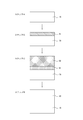
- 6A to 6D are process diagrams with schematic cross-sectional views for explaining a method of manufacturing a reflective electrode for a deep ultraviolet light emitting device according to an embodiment of the present invention.
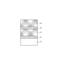
- 6A to 6C are process diagrams with schematic cross-sectional views for explaining a method of manufacturing a reflective electrode for a deep ultraviolet light emitting device according to another embodiment of the present invention.
- 1 is a schematic cross-sectional view illustrating a deep ultraviolet light emitting device according to an embodiment of the present invention.
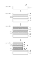
- 6A to 6C are process diagrams with schematic cross-sectional views for explaining the method for manufacturing the deep-UV light emitting device according to the embodiment of the present invention.
- AlGaN the composition ratio of the group III element (total of Al and Ga) and N is 1:1 and the group III element is The ratio of Al to Ga means any arbitrary compound.
- AlGaN may include In within 5% of the total of Al and Ga as the group III elements, even if there is no description about In as the group III element.
- the Al composition ratio is x 0 and the In composition ratio is y 0 (0 ⁇ y 0 ⁇ 0.05), and Al x0 In y0 Ga 1 -x0-y0 N.
- AlN When simply expressed as “AlN” or “GaN”, it means that Ga and Al are not included, respectively, but unless otherwise specified, simply expressed as “AlGaN” means either AlN or GaN. It does not preclude something.
- the value of the Al composition ratio can be measured by photoluminescence measurement, X-ray diffraction measurement, or the like.
- a layer that electrically functions as p-type is referred to as a p-type layer
- a layer that electrically functions as n-type is referred to as an n-type layer.
- a specific impurity such as Mg or Si is not intentionally added and does not electrically function as p-type or n-type, it is referred to as “i-type” or “undoped”.
- the undoped layer may contain impurities that are unavoidable in the manufacturing process. Specifically, when the carrier density is low (for example, less than 4 ⁇ 10 16 /cm 3 ), it is referred to as “undoped” in the present specification. To call.
- the value of the impurity concentration of Mg, Si, or the like is based on SIMS analysis.
- the total thickness of each layer formed by epitaxial growth can be measured using an optical interference type film thickness meter. Further, the thickness of each layer can be calculated by observing the cross section of the growth layer with a transmission electron microscope when the compositions of the adjacent layers are sufficiently different (for example, the Al composition ratio is different by 0.01 or more). Regarding the boundaries and thicknesses of adjacent layers having the same or almost equal Al composition ratios (for example, less than 0.01) but different impurity concentrations, the boundaries between the two and the thickness of each layer The measurement is based on TEM-EDS. The impurity concentrations of both can be measured by SIMS analysis. When the thickness of each layer is thin like a superlattice structure, the thickness can be measured using TEM-EDS.
- FIG. 1A shows a p-side reflective electrode 80 obtained by a method of manufacturing a reflective electrode for a deep ultraviolet light emitting device according to an embodiment of the present invention.
- FIG. 2 is a schematic sectional view of a deep ultraviolet light emitting device 100 having this reflective electrode 80.
- the reflective electrode 80 can be provided directly on the p-type contact layer 70.
- the reflective electrode 80 is a reflective electrode that uses a metal having a high reflectance (for example, 60% or more) with respect to the ultraviolet light emitted from the light emitting layer 40, and has such a reflectance in the present invention.
- Rhodium (Rh) is used as the metal (hereinafter, referred to as “reflection metal”).
- rhodium (Rh) for example, commercially available metal rhodium (for example, purity 3N) can be used as a vapor deposition source.
- the p-type contact layer 70 has a superlattice structure, and nickel (Ni) having a certain thickness or more is formed on the p-type contact layer 70 to form the reflective metal on the p-side.
- the reflective electrode has a high reflectance for deep ultraviolet light. Furthermore, by performing a heat treatment at 300° C. or more and 600° C.
- the reflectance of the reflective electrode 80 is the same as the first metal layer 81 and the second metal layer 81 on the sapphire substrate.
- the metal layer 82 is formed, and light of each wavelength is irradiated from the transparent sapphire substrate side toward the reflective electrode 80 before and after the heat treatment step, and the reflectance (for example, wavelength It shall be substituted by measuring the reflectance for 300 nm).
- a method of manufacturing a reflective electrode for a deep ultraviolet light emitting device is characterized in that a p-type contact layer 70 having a superlattice structure (step 1A in FIG. 1A)
- the first step (FIG. 1A step 1B) of forming Ni as the first metal layer 81 with a thickness of 3 to 20 nm, and the Rh as the second metal layer 82 on the first metal layer 81 with a thickness of 20 nm or more and 2 ⁇ m or less.
- a second step of forming step 1C in FIG. 1A
- a third step step 1D in FIG. 1A of performing heat treatment at 300° C. or more and 600° C. or less on the first metal layer and the second metal layer. Equipped.
- Ni is formed as the first metal layer 81 on the p-type contact layer 70 to a thickness of 3 to 20 nm.
- Ni can be deposited on the surface of the p-type contact layer 70 by a general method such as a vacuum deposition method such as an electron beam deposition method and a resistance heating deposition method, and a sputtering method. This is because if the thickness is less than 3 nm, it is difficult to suppress the above-mentioned death, and if the thickness exceeds 20 nm, the reflectance of the reflective electrode significantly decreases. Further, the thickness of the first metal layer 81 is more preferably 3 to 10 nm.
- the reflectance of the reflective electrode 80 after the heat treatment for the wavelength of 300 nm can be 60% or more.
- the thickness of the first metal layer 81 can be measured using a film thickness meter of a crystal oscillator.
- Rh is formed on the first metal layer 81 as the second metal layer 82 with a thickness of 20 nm or more and 2 ⁇ m or less. This is because if the thickness is less than 20 nm, the reflectance of the second metal layer 82 against ultraviolet light may not be sufficiently high. Further, if it exceeds 2 ⁇ m, there is a problem of cost for Rh.
- the thickness of the second metal layer 82 is more preferably 30 nm or more in order to improve the reflectance of the reflective electrode after the diffusion of the first metal layer 81 by the heat treatment process described later, and is 100 nm or less to reduce the cost. More preferably.
- the second step can also form the second metal layer by a general method such as a vacuum deposition method and a sputtering method.
- the thickness of the second metal layer 82 can be measured using a crystal oscillator film thickness meter.
- the first metal layer 81 and the second metal layer 82 are heat-treated at 300° C. or higher and 600° C. or lower to obtain the reflective electrode 80.
- an inert gas such as nitrogen
- the inert gas may be used as the atmospheric gas.
- the atmospheric gas contains oxygen.
- the flow rate ratio of oxygen in the atmosphere gas is preferably more than 0% and 50% or less.
- the reflective electrode 80 thus obtained is an electrode made of Ni and Rh.
- Ni as the first metal layer 81 diffuses from the interface in contact with the p-type contact layer 70 to the Rh side of the second metal layer 82.
- the proportion of Rh at the interface between the p-type contact layer 70 and the reflective electrode 80 increases due to the diffusion of Ni, the reflectance at the interface increases as compared to before the heat treatment.
- Ni does not maintain a layered state and diffuses, so it is difficult to accurately measure the amount of Ni after the heat treatment (that is, after diffusion).
- Rh is 50% or more, preferably 75% or more, in terms of volume ratio (corresponding to the area ratio in the SEM-EDS analysis mapping of the cross section of the reflective electrode).
- the reflectance of Rh simple substance at a wavelength of 300 nm is 70 to 73%, and the reflectance of the alloy of Ni and Au is less than 40%.
- the reflective electrode 80 made of Ni and Rh according to the invention has a reflectance of 40 nm at a wavelength of 300 nm by setting the thickness of the first metal layer 81 to 3 to 20 nm and the thickness of the second metal layer 82 to 20 nm to 2 ⁇ m. % And less than 67%, the reflectance of the first metal layer 81 is 3 to 10 nm, and the thickness of the second metal layer 82 is 30 nm to 100 nm. Can be 60% or more and less than 70%.
- ruthenium (Ru), gold (Au), platinum (Pt), palladium (Pd), titanium (Ti) are included as impurities that may be contained other than Ni and Rh and do not significantly reduce the reflectance. It is considered that the content of impurities is 40% by mass or less, preferably 10% by mass or less.
- the reflective electrode 80 for the deep ultraviolet light emitting device according to the present embodiment described above in the deep ultraviolet light emitting device it is possible to achieve both high light emission output and excellent reliability.
- a step of forming a Ni layer as the third metal layer 83 on the second metal layer after the second step, and a fourth metal layer 84 on the third metal layer 83 It is also preferable to further include the step of forming the Rh layer. This step may be performed between the second step and the third step or after the third step, but work efficiency should be performed immediately after the second step between the second step and the third step.
- a Ni layer can be formed with a thickness of 1 to 20 nm.
- the Rh layer as the fourth metal layer 84 can be formed with a thickness of 5 nm or more and 2 ⁇ m or less.
- the Ni layer and the Rh layer corresponding to the third metal layer and the fourth metal layer are formed again on the fourth metal layer 84, and the reflective electrode is formed a plurality of times in the order of the Ni layer and the Rh layer. It may be a laminated body formed by repeatedly laminating.
- the reflective electrode composed of Ni and Rh may be replaced by Ni and Rh.
- the Ni layer and the Rh layer are stacked a plurality of times, a mounting process of connecting another metal (such as gold) on the Rh layer after the stacking to form an electrical connection with the outside and a connection with the outside. It is preferable because the electrode can be more surely avoided without fear of death, regardless of the method (including the case of requiring heating such as solder). From this point of view, it is particularly preferable that the metal element forming the reflective electrode is composed of only Ni and Rh.
- a deep ultraviolet light emitting device 100 includes an n-type semiconductor layer 30, a light emitting layer 40, a p-type electron blocking layer 60 and a p-type contact layer 70 on a substrate 10, and This is a deep-ultraviolet light-emitting element having the p-side reflective electrode 80 in order.
- the reflective electrode 80 is provided on the outermost second layer 72 of the p-type contact layer.
- the p-type contact layer 70 includes a first layer 71 made of Al x Ga 1-x N having an Al composition ratio x, and a second layer 72 made of Al y Ga 1-y N having an Al composition ratio y. It has a superlattice structure formed by alternately stacking.
- the Al composition ratio y of the second layer 72 is 0.15 or more (y ⁇ 0.15).
- the Al composition ratio x of the first layer 71 is higher than the Al composition ratio w 0
- the Al of the second layer 72 is Al.
- the composition ratio y is lower than the Al composition ratio x
- the Al composition ratio w 0 , the Al composition ratio x, the Al composition ratio y, and the thickness average Al composition ratio z of the p-type contact layer 70 are represented by the following formulas [1] and [2]. ]: 0.030 ⁇ zw 0 ⁇ 0.20... [1] 0.050 ⁇ xy ⁇ 0.47... [2] It is preferable to satisfy
- the buffer layer 20 is provided between the substrate 10 and the n-type semiconductor layer 30, the p-side reflective electrode 80 is provided directly above the p-type contact layer 70, and the n-type semiconductor layer 30 is provided.
- Providing the n-side electrode 90 on the exposed surface is a preferred embodiment of the deep ultraviolet light emitting device 100.
- the Al composition ratio and thickness of each of the first layer 71 and the second layer 72 in the superlattice structure of the p-type contact layer 70 are assumed to be constant.
- the thickness average Al composition ratio z of the p-type contact layer 70 is defined as follows. First, the number of layers of the first layer 71 in the super lattice structure is N, representing the thickness of each layer of the first layer 71 and t a. Similarly, the number of layers of the second layer 72 is M, and the thickness of each layer of the second layer 72 is represented by t b . At this time, the thickness average Al composition ratio z of the p-type contact layer 70 is according to the following formula [3].
- the Al composition ratios and thicknesses of the first layer 71 and the second layer 72 in the superlattice structure of the p-type contact layer 70 do not necessarily have to be constant.
- the thickness average Al composition ratio z is equal to the thickness of each of the first layer 71 and the second layer 72.
- a weighted average value (weighted average value) depending on the Al composition ratio may be used, and the Al composition ratios x and y of the first layer 71 and the second layer 72 refer to the weighted average value depending on the thickness. To do.
- the details of each structure of the substrate 10, the n-type semiconductor layer 30, the light-emitting layer 40, the p-type electron blocking layer 60, and the p-type contact layer 70 in the deep ultraviolet light emitting device 100 will be described first.
- ⁇ Substrate> As the substrate 10, it is preferable to use a substrate capable of transmitting light emitted from the light emitting layer 40, and for example, a sapphire substrate or a single crystal AlN substrate can be used. Alternatively, as the substrate 10, an AlN template substrate in which an undoped AlN layer is epitaxially grown on the surface of a sapphire substrate may be used.
- the n-type semiconductor layer 30 is provided on the substrate 10 via the buffer layer 20 if necessary.
- the n-type semiconductor layer 30 may be directly provided on the substrate 10.
- the n-type semiconductor layer 30 is doped with an n-type dopant.
- Specific examples of the n-type dopant include silicon (Si), germanium (Ge), tin (Sn), sulfur (S), oxygen (O), titanium (Ti), zirconium (Zr), and the like.
- the dopant concentration of the n-type dopant is not particularly limited as long as the dopant concentration allows the n-type semiconductor layer 30 to function as the n-type, and is, for example, 1.0 ⁇ 10 18 atoms/cm 3 to 1.0 ⁇ 10 20.
- the band gap of the n-type semiconductor layer 30 is wider than the band gap of the light emitting layer 40 (the well layer 41 in the case of a quantum well structure), and it is preferable that the n type semiconductor layer 30 be transmissive to the emitted deep ultraviolet light.
- the n-type semiconductor layer 30 may have a single-layer structure or a structure having a plurality of layers, as well as a composition-graded layer in which the composition ratio of the group III element is compositionally graded in the crystal growth direction, or a superlattice structure.
- the n-type semiconductor layer 30 not only forms a contact portion with the n-side electrode but also has a function of enhancing crystallinity from the substrate to the light emitting layer.
- the light emitting layer 40 is provided on the n-type semiconductor layer 30 and emits deep ultraviolet light.
- the light emitting layer 40 can be made of AlGaN, and the Al composition ratio thereof is set so that the wavelength of emitted light is 200 to 350 nm of deep ultraviolet light or the central emission wavelength is 265 nm or more and 317 nm or less. You can Such an Al composition ratio can be set in the range of 0.25 to 0.60, for example.
- the light emitting layer 40 may have a single-layer structure with a constant Al composition ratio, or may be a multiple quantum well (MQW) formed by repeatedly forming a well layer 41 and a barrier layer 42 made of AlGaN having different Al composition ratios. It is also preferable to construct the structure.
- MQW multiple quantum well
- the Al composition ratio w 0 of the layer that emits deep ultraviolet light in the light emitting layer 40 is the Al composition ratio itself of the light emitting layer 40.
- the well layer 41 corresponds to a layer that emits deep ultraviolet light in the light emitting layer 40.
- the Al composition ratio w of the well layer 41 is the above Al composition. Treat as equivalent to the ratio w 0 .
- the Al composition ratio w) is preferably 0.25 to 0.60.
- the Al composition ratio b of the barrier layer 42 is set higher than the Al composition ratio w of the well layer 41 (that is, b>w).
- the Al composition ratio b of the barrier layer 42 can be set to 0.40 to 0.95, for example.
- the number of repetitions of the well layer 41 and the barrier layer 42 is not particularly limited and can be set to 1 to 10 times, for example. It is preferable that both ends (that is, the first and last) in the thickness direction of the light emitting layer 40 be barrier layers, and when the number of repetitions of the well layer 41 and the barrier layer 42 is n, in this case, “n. And barrier layer”.
- the well layer 41 can have a thickness of 0.5 nm to 5 nm
- the barrier layer 42 can have a thickness of 3 nm to 30 nm.
- the barrier layer 42 and the p-type layer are provided between the well layer 41 closest to the p-type electron block layer 60 in the light-emitting layer 40 and the p-type electron block layer 60 described later. It is also preferable to provide a guide layer having a higher Al composition ratio than any one of the electron block layers 60. Thereby, the light emission output of the deep ultraviolet light emitting device 100 can be increased.
- the Al composition ratio of the guide layer is expressed as b g and the Al composition ratio ⁇ of the p-type electron block layer 60 described later is used, the relationship of each Al composition ratio is as follows. w (well layer) ⁇ b (barrier layer) ⁇ (p-type electron block layer) ⁇ b g (guide layer)
- the light emitting layer 40 is the n sets of well layers 41 and the barrier layers 42 starting from the barrier layer 42, and the layer in contact with both the light emitting layer 40 and the p-type electron blocking layer 60 is the above-mentioned guide layer, and the thickness thereof is different.
- the barrier layer is thinner than the barrier layer.
- the guide layer is made of AlN (in this case, particularly referred to as an AlN guide layer), and the thickness thereof is 0.7 to 1.7 nm.
- the p-type electron block layer 60 is provided on the light emitting layer 40.
- the p-type electron block layer 60 is used as a layer for blocking electrons and injecting the electrons into the light emitting layer 40 (the well layer 41 in the case of the MQW structure) to improve the electron injection efficiency.
- the Al composition of the p-type electron block layer 60 The ratio ⁇ is preferably 0.35 ⁇ 0.95.
- the p-type electron block layer 60 may include In in an amount of 5% or less with respect to Al and Ga as group III elements.
- the Al composition ratio ⁇ is preferably higher than the thickness average Al composition ratio z of the p-type contact layer 70 while satisfying the above conditions. That is, it is preferable that ⁇ >z.
- both of the Al composition ratio ⁇ of the p-type electron block layer 60 and the Al composition ratio b of the barrier layer 42 satisfy 0 ⁇ b ⁇ 0.55. By doing so, the efficiency of electron injection into the well layer 41 by the p-type electron block layer 60 can be reliably increased.
- the thickness of the p-type electron blocking layer 60 is not particularly limited, but is preferably 10 nm to 80 nm, for example. When the thickness of the p-type electron block layer 60 is in this range, a high light emission output can be reliably obtained.
- the thickness of the p-type electron block layer 60 is preferably larger than that of the barrier layer 42.
- Examples of the p-type dopant with which the p-type electron block layer 60 is doped include magnesium (Mg), zinc (Zn), calcium (Ca), beryllium (Be), manganese (Mn), and the like. Is generally used.
- the dopant concentration of the p-type electron block layer 60 is not particularly limited as long as it is a dopant concentration that can function as a p-type layer, and is, for example, 1.0 ⁇ 10 18 atoms/cm 3 to 5.0 ⁇ 10 21 atoms/. It can be cm 3 .
- the p-type contact layer 70 is provided on the p-type electron block layer 60.
- the p-type contact layer 70 is a layer for reducing the contact resistance between the p-side reflective electrode 80 provided immediately above and the p-type electron block layer 60. Therefore, there is no desired structure between the p-type contact layer 70 and the p-side reflective electrode 80 other than impurities that are unavoidable in manufacturing. That is, the p-side reflective electrode 80 is in contact with the p-type contact layer 70 having the superlattice structure.
- the p-type contact layer 70 is formed by alternately stacking the first layers 71 made of Al x Ga 1-x N and the second layers 72 made of Al y Ga 1-y N. It has a superlattice structure.
- the Al composition ratio x of the first layer 71 is made higher than the Al composition ratio w 0 of the layer that emits deep ultraviolet light in the light emitting layer 40 (x>w 0 ), and the transmittance for deep ultraviolet light is set. It is preferable to increase.
- the Al composition ratio x may be set higher than the Al composition ratio of the light emitting layer 40.
- the Al composition ratio x may be set to the well layer 41. It may be higher than the Al composition ratio w.
- the Al composition ratio w 0 , the Al composition ratio x, the Al composition ratio y, and the thickness average Al composition ratio z of the p-type contact layer are represented by the following formulas [1] and [2]: 0.030 ⁇ zw 0 ⁇ 0.20... [1] 0.050 ⁇ xy ⁇ 0.47... [2] It is preferable to satisfy
- the prior art it was general to use a p-type GaN layer that is easy to increase the hole concentration as a p-type contact layer of a deep ultraviolet light emitting device.
- the p-type GaN layer absorbs light having a wavelength of 360 nm or less due to its band gap. Therefore, of the deep ultraviolet light emitted from the light emitting layer, the light extraction effect from the p-type contact layer side or the light extraction effect by reflection at the p-side electrode can hardly be expected.
- the p-type contact layer is made of AlGaN having a high Al composition ratio
- the hole concentration can be reduced to some extent as compared with GaN, but since deep ultraviolet light emitted from the light emitting layer can pass through the p-type contact layer.
- the light extraction efficiency of the deep ultraviolet light emitting device as a whole is improved, and as a result, the light emission output of the deep ultraviolet light emitting device can be increased.
- the Al composition ratio of the p-type contact layer becomes too high, a deep-ultraviolet light emitting device with insufficient reliability can be obtained.
- the thickness average Al composition ratio z is larger than the Al composition ratio w 0 of the layer that emits deep ultraviolet light in the light emitting layer 40. Is high (z>w 0 ), deep ultraviolet light can pass through the p-type contact layer 70, and as a result, a higher emission output can be obtained, which is preferable.
- the thickness average Al composition ratio z and the Al composition ratio w of the layer that emits deep ultraviolet light are calculated according to the above formula [1]. It is preferable to make the difference of 0.030 higher than 0.030 (that is, z ⁇ w 0 >0.030). For this purpose, it is more preferable that the difference between the Al composition ratio z and the Al composition ratio w is higher than 0.040 (z ⁇ w 0 >0.040), and higher than 0.050 (z ⁇ w 0 >0.050) is more preferable, and higher than 0.06 (z ⁇ w 0 >0.060) is particularly preferable.
- the upper limit of the difference between the thickness average Al composition ratio z and the Al composition ratio w of the layer that emits deep ultraviolet light is more preferably 0.19 (z ⁇ w 0 ⁇ 0.19), and the upper limit is 0.1. More preferably, it is 18 (zw 0 ⁇ 0.18).
- the difference between the Al composition ratio x of the first layer 71 and the Al composition ratio y of the second layer 72 is 0.050 or more in absolute value (xy ⁇ 0.050). It is preferable. This is to ensure that the p-type contact layer 70 functions as a superlattice structure. Further, since the strain of the entire superlattice structure is reduced and the p-side reflective electrode 80 is brought into contact with a low Al composition ratio, the difference between the Al composition ratio x and the Al composition ratio y is 0.1 or more (x ⁇ y ⁇ 0.10) is preferable, and 0.15 or more (xy ⁇ 0.15) is more preferable.
- the Al composition ratio y of the second layer 72 which is a layer having a low Al composition ratio in the superlattice structure, is 0.20 or more, the transmittance of deep ultraviolet light from the light emitting layer 40 can be increased more reliably. It is possible and preferable.
- the Al composition ratio y is more preferably 0.21 or more, further preferably 0.25 or more.
- the Al composition ratio y is more preferably 0.51 or less. It is particularly preferable to set it to 0.40 or less.
- the Al composition ratio y may be higher or lower than the Al composition ratio w 0. Good.
- the Al composition ratio x may be appropriately set as long as it satisfies the above formulas [1] and [2], and the upper limit and the lower limit of the Al composition ratio x are not limited. After satisfying the expressions [1] and [2], the Al composition ratio x may be set within the range of approximately 0.40 to 0.85.
- each of the thickness t a of the first layer 71 and second layer 72, t b form a superlattice structure, and the thickness of the average Al composition z, the conditions for the Al composition ratio of the light-emitting layer 40
- the thickness t a of the first layer 71 can be a 1.0nm or 10.0nm or less
- the thickness t b of the second layer 72 can be 1.0nm or 10.0nm or less.
- the size relationship between the thicknesses t a and t b is not limited, and either one may be larger, or both thicknesses may be the same.
- the number of repetitions of the first layer 71 and the second layer 72 is set to, for example, 3 to 15 times so that the total thickness of the p-type contact layer 70 is in the range of 20 nm or more and 100 nm or less, preferably 70 nm or less. It is preferable to set it appropriately within the range.
- the total thickness of the p-type layer which is the total thickness of the p-type electron blocking layer 60 and the p-type contact layer 70, is preferably 65 nm or more and 100 nm or less, and 70 nm or more and 95 nm or less. Is more preferable. Within this range, a high light emission output can be obtained more reliably.
- the end layer closer to the p-type electron block layer 60 is preferably the first layer 71.
- the first layer is formed directly on the p-type electron block layer 60.
- 71 is preferably provided.
- the Al composition ratio x of the first layer 71 is higher than the Al composition ratio y of the second layer 72, and the Al composition ratio x is closer to the Al composition ratio ⁇ of the p-type electron block layer 60. It is possible to more reliably suppress generation of defects due to strain between the layer 60 and the p-type contact layer 70.
- the end layer farther from the p-type electron block layer 60 is preferably the second layer 72.
- the layer in contact with the p-side reflective electrode 80 is preferably the second layer 72. This is because when the Al composition ratio x of the first layer 71 and the Al composition ratio y of the second layer 72 are compared, the Al composition ratio y is lower, so that ohmic contact with the p-side reflective electrode 80 is facilitated. ..
- the end layer closer to the p-type electron block layer 60 in the thickness direction of the p-type contact layer 70 is the first layer 71, and the end layer farther from the p-type electron block layer 60 is the first layer 71.
- the number of layers of the first layer 71 and the number of layers of the second layer 72 are the same. However, in this embodiment, the numbers of layers of both do not necessarily match.
- the number of the second layers 72 is 1 compared to the number of the first layers 71). Including many layers).
- the superlattice structure in which the two layers of the first layer 71 and the second layer 72 are repeatedly laminated has been described so far, but as another embodiment according to the present invention, the above-mentioned first A superlattice having a three-layer structure in which a third layer having an Al composition ratio between the first layer and the second layer is arranged between the first layer and the second layer while having the same relationship between the first layer and the second layer.
- the structure can also be applied. Also in this case, the same effects as the effects of the present invention described above can be obtained.
- the p-type contact layer 70 preferably has a high-concentration region having a Mg concentration of 3 ⁇ 10 20 atoms/cm 3 or more on the side in contact with the p-side reflective electrode 80. It is more preferably 5 ⁇ 10 20 atoms/cm 3 or more.
- the hole concentration of the p-type contact layer 70 can be increased to reduce the forward voltage Vf of the deep ultraviolet light emitting device 100.
- the upper limit of the Mg concentration in the high concentration region can be set to 1 ⁇ 10 21 atoms/cm 3 in the present embodiment.
- the Mg concentration in the region of the p-type contact layer 70 on the p-type electron blocking layer 60 side can be set in a general range, and is usually 5 ⁇ 10 19 atoms/cm 3 or more and 3 ⁇ 10 20 atoms/cm 3 Is less than.
- the Mg concentration in the p-type contact layer is the average concentration in each region measured by SIMS.
- the thickness of the high concentration region is usually 15 nm or less, and a few layers on the side in contact with the p-side reflective electrode 80 can be the high concentration region.
- the p-type contact layer 70 may have a Si-doped region having a Si concentration of 5 ⁇ 10 16 atoms/cm 3 or more and 1 ⁇ 10 20 atoms/cm 3 or less on the side in contact with the p-side reflective electrode 80.
- the Si concentration in the region is 2 ⁇ 10 19 atoms/cm 3 or more and 5 ⁇ 10 19 atoms/cm 3 or less. By doing so, the light emission output of the deep ultraviolet light emitting device 100 can be further increased. If the thickness of the Si-doped region is about 1 to 5 nm, this effect can be surely obtained.
- the Si-doped region is the last second layer in the superlattice structure of the p-type contact layer.
- a co-doped region may be formed by further doping Si into the high-concentration region where the Mg concentration is 3 ⁇ 10 20 atoms/cm 3 or more. Further, the Si-doped region may be doped with only Si (that is, Mg may not be doped).
- the region when a Si-doped region doped with only Si is provided on the side of the p-type contact layer 70 in contact with the reflection electrode 80 on the p-side and the region is not doped with Mg, the region is considered to be n-type as the conductivity type. You can think. However, in the case of the above thickness range (1 to 5 nm), even if Mg is not doped, it does not become a thyristor if it contacts the p-type electrode as the uppermost layer of the p-type contact layer 70. Therefore, even in such a case, the Si-doped region is regarded as a part of the p-type contact layer 70.
- the deep ultraviolet light emitting device 100 according to the present embodiment described above can achieve both high emission output and excellent reliability.
- ⁇ Buffer layer> As shown in FIG. 2, it is also preferable to provide a buffer layer 20 between the substrate 10 and the n-type semiconductor layer 30 to reduce the lattice mismatch between the two.
- An undoped group III nitride semiconductor layer can be used as the buffer layer 20, and the buffer layer 20 preferably has a superlattice structure.
- the n-side electrode 90 that can be provided on the exposed surface of the n-type semiconductor layer 30 can be, for example, a metal composite film including a Ti-containing film and an Al-containing film formed on the Ti-containing film.
- the thickness, shape and size of the n-side electrode 90 can be appropriately selected according to the shape and size of the light emitting element.
- the n-side electrode 90 is not limited to being formed on the exposed surface of the n-type semiconductor layer 30 as shown in FIG. 2, but may be electrically connected to the n-type semiconductor layer.
- a guide layer made of AlGaN having a higher Al composition ratio than the Al composition ratio ⁇ of the p-type electron block layer 60 is provided between the light emitting layer 40 and the p-type electron block layer 60. It may be provided. By providing the guide layer, injection of holes into the light emitting layer 40 can be promoted.
- a p-type clad layer made of AlGaN may be provided between the p-type electron block layer 60 and the p-type contact layer 70.
- the p-type cladding layer is higher than the Al composition ratio of the layer that emits deep ultraviolet light in the light emitting layer 40 (Al composition ratio w in the case of the quantum well structure) and the thickness average Al composition ratio z of the p-type contact layer 70.
- Al composition ratio w Al composition ratio in the case of the quantum well structure
- it is a layer having an Al composition ratio lower than the Al composition ratio ⁇ of the p-type electron block layer 60.
- both the p-type electron blocking layer 60 and the p-type cladding layer are layers having an Al composition ratio higher than the Al composition ratio of the layer that emits deep ultraviolet light, and the deep ultraviolet light emitted from the light emitting layer 40 is emitted. It is a substantially transparent layer. However, it is preferable not to provide the p-type cladding layer. The reason for this is as described in JP-A-2016-111370, and the entire disclosure content thereof is incorporated herein by reference.
- the p-type clad layer when the Al composition ratio of the p-type clad layer is ⁇ , ⁇ > ⁇ and ⁇ >y.
- the substrate side or the substrate horizontal direction is the main light extraction direction by forming the p-side reflective electrode 80 with a reflective electrode material and reflecting the deep ultraviolet light. be able to. Further, the deep ultraviolet light emitting device 100 can be in a so-called flip chip type.
- One embodiment of the method for manufacturing the deep ultraviolet light emitting device 100 according to the present invention is a process of forming the n-type semiconductor layer 30 on the substrate 10 (see step 3A in FIG. 3), and a light emitting layer 40 on the n-type semiconductor layer 30. , A step of forming the p-type electron block layer 60 on the light emitting layer 40 (see step 3B in FIG. 3), and a step of forming a p-type contact layer on the p-type electron block layer (step in FIG. 3).
- the step of forming the p-type contact layer includes a first step of forming a first layer of Al x Ga 1-x N having an Al composition ratio x, and an Al composition ratio lower than the Al composition ratio x.
- the second step of forming a second layer of Al y Ga 1-y N having y is alternately repeated to form the p-type contact layer having a superlattice structure, and the Al of the second layer is formed.
- the composition ratio y is 0.15 or more.
- Ni is used as the first metal layer 81 with a thickness of 3 to 20 nm on the p-type contact layer 70 having the superlattice structure.
- a first step of forming, a second step of forming Rh as a second metal layer 82 on the first metal layer 81 with a thickness of 20 nm or more and 2 ⁇ m or less, and with respect to the first metal layer and the second metal layer And a third step of performing heat treatment at 300° C. or higher and 600° C. or lower (see FIG. 1A).
- the step of forming the p-type contact layer 70 includes the first step of forming the first layer 71 of Al x Ga 1-x N having the Al composition ratio x and the Al composition ratio x. And a second step of forming a second layer 72 made of Al y Ga 1-y N having a low Al composition ratio y is alternately repeated to form a p-type contact layer 70 having a superlattice structure.
- the Al composition ratio y of the second layer 72 is 0.15 or more (y ⁇ 0.15).
- the Al composition ratio of the layer that emits deep ultraviolet light in the light emitting layer 40 is w 0
- the Al composition ratio x of the first layer 71 is higher than the Al composition ratio w 0
- the Al of the second layer 72 is Al.
- the composition ratio y is lower than the Al composition ratio x
- the Al composition ratio w 0 , the Al composition ratio x, the Al composition ratio y, and the thickness average Al composition ratio z of the p-type contact layer 70 are represented by the following formulas [1] and [2]. ]: 0.030 ⁇ zw 0 ⁇ 0.20... [1] 0.050 ⁇ xy ⁇ 0.47... [2] It is preferable to satisfy
- each layer can be formed by a known epitaxial growth technique such as a metal organic chemical vapor deposition (MOCVD) method, a molecular beam epitaxy (MBE) method, and a sputtering method. ..
- MOCVD metal organic chemical vapor deposition
- MBE molecular beam epitaxy
- the growth temperature, growth pressure, and growth time for epitaxial growth depend on the Al composition ratio and thickness of each layer. Can be general conditions.
- a carrier gas for epitaxial growth hydrogen gas, nitrogen gas, a mixed gas of the two, or the like may be used and supplied into the chamber.
- a source gas for growing each of the above layers TMA (trimethylaluminum), TMG (trimethylgallium), or the like can be used as a group III element source gas, and NH 3 gas can be used as a group V element gas.
- V/III ratio Molar ratio of group V element to group III element calculated based on the growth gas flow rate of group V element gas such as NH 3 gas and group III element gas such as TMA gas
- group V element gas such as NH 3 gas and group III element gas such as TMA gas
- the general conditions may be applied.
- the gas of the dopant source for the p-type dopant, cyclopentadiene magnesium gas (CP 2 Mg) or the like for the Mg source, and for the n-type dopant, for example, monosilane gas (SiH 4 ) or the Zn source as the Si source.
- Zinc chloride gas (ZnCl 2 ) or the like may be appropriately selected and supplied into the chamber at a predetermined flow rate.
- the p-type contact layer 70 having a superlattice structure in which the first layer 71 and the second layer 72 described above are repeated on the p-type electron block layer 60.
- the conditions for the thickness range and the Al composition ratio of the p-type contact layer 70 are as described above.
- the p-type contact layer 70 may be crystal-grown by epitaxial growth such as MOCVD.
- the following processing may be performed. That is, in the p-type contact layer forming step, the above-mentioned superlattice structure is crystal-grown by supplying the group III source gas, the group V source gas, and the Mg source gas, and the flow rate of the group III source gas is changed immediately after the crystal growth is completed.
- the flow rate may be reduced to 1/4 or less of the flow rate during crystal growth, and the group V source gas and the Mg source gas may be continuously supplied for 1 minute to 20 minutes.
- CP 2 Mg gas is supplied to the chamber as the Mg source and monosilane gas ( SiH 4 ) or the like may be flowed. If only Si is to be doped, the CP 2 Mg gas as the Mg source may be stopped from being supplied to the chamber, and the monosilane gas (SiH 4 ) may be allowed to flow as the Si source.
- Si is doped on the p-side contact layer 70 on the side in contact with the reflective electrode 80 as described above, the formation of the Mg high-concentration region is optional.
- n-side electrode is formed on the exposed n-type semiconductor layer 30.
- 90 can be formed.
- the n-side electrode 90 can be formed by a sputtering method, a vacuum vapor deposition method, or the like. It is also preferable to form the buffer layer 20 on the surface 10A of the substrate 10.
- Example 1 A deep ultraviolet light emitting device according to Inventive Example 1 was produced according to the process diagrams shown in FIGS. 1A and 3.
- a sapphire substrate (diameter: 2 inches, thickness: 430 ⁇ m, plane orientation: (0001)) was prepared.
- an AlN layer having a central film thickness of 0.60 ⁇ m was grown on the sapphire substrate by MOCVD method to obtain an AlN template substrate.
- the growth temperature of the AlN layer was 1300° C.
- the growth pressure in the chamber was 10 Torr
- the growth gas flow rates of the ammonia gas and the TMA gas were set so that the V/III ratio was 163.
- film thickness of the AlN layer a total of 25 film thicknesses were dispersed at equal intervals, including the center of the wafer, using an optical interference film thickness measuring device (Nanospec M6100A; manufactured by Nanometrics). Was measured.
- the above AlN template substrate was introduced into a heat treatment furnace, and after the inside of the furnace was made into a nitrogen gas atmosphere, the temperature inside the furnace was raised and the heat treatment was applied to the AlN template substrate. At that time, the heating temperature was 1650° C. and the heating time was 4 hours.
- a buffer layer of undoped Al 0.55 Ga 0.45 N having a thickness of 1 ⁇ m was formed by MOCVD.
- an Si-doped n-type semiconductor layer having a thickness of 2 ⁇ m and made of Al 0.45 Ga 0.55 N was formed on the buffer layer.
- the Si concentration of the n-type semiconductor layer was 1.0 ⁇ 10 19 atoms/cm 3 .
- n-type semiconductor layer three sets of well layers of Al 0.29 Ga 0.71 N and a thickness of 3 nm and barrier layers of Al 0.51 Ga 0.49 N and a thickness of 7 nm are alternately repeated on the n-type semiconductor layer.
- the Al composition ratio w of the well layer is 0.29.
- a guide layer having a thickness of 1 nm was formed from AlN on the light emitting layer. Note that Si was doped when forming the barrier layer and undoped when forming the well layer and the guide layer.
- a 40-nm-thick p-type electron block layer made of Al 0.58 Ga 0.42 N was formed on the guide layer using hydrogen gas as a carrier gas.
- CP 2 Mg gas was supplied to the chamber as a Mg source to dope Mg.
- the Mg concentration of the p-type electron block layer was 5.0 ⁇ 10 18 atoms/cm 3 .
- Al 0.47 Ga 0.53 N is formed as a first layer immediately above the p-type electron block layer, and then Al 0.31 Ga 0.69 N is formed as a second layer, and both are formed.
- Al 0.47 Ga 0.53 N is formed as a first layer immediately above the p-type electron block layer
- Al 0.31 Ga 0.69 N is formed as a second layer, and both are formed.
- the thickness of the first layer is 5.0 nm
- the thickness of the second layer is 2.5 nm
- the total thickness of the p-type contact layers is 52.5 nm
- the average Al composition of the thickness is 0. 42.
- CP 2 Mg gas as a Mg source is supplied to the chamber together with the group III source TMA gas, the TMG gas, and the group V source ammonia gas, and the p type contact layer is doped with Mg. Was grown. Then, only the supply of the group III source gas was stopped, and only the Mg source gas and the group V source gas were supplied for 10.5 minutes to form a high concentration region on the surface side of the p-type contact layer.
- the Al composition ratio of the p-type contact layer was determined from the emission wavelength (bandgap energy) of the p-type contact layer analyzed by photoluminescence measurement.
- the Mg concentration on the p-type electron block layer side was 1 ⁇ 10 20 atoms/cm 3 , and the surface forming the p-side reflective electrode 80 opposite to the p-type electron block layer.
- the Mg concentration on the side where the Mg concentration on the side was high (high concentration region) was 3 ⁇ 10 20 atom/cm 3 .
- Table 1 shows the layer structure of Example 1.
- a mask was formed on the p-type contact layer and mesa etching was performed by dry etching to expose the n-type semiconductor layer. Then, a Ni layer (first metal layer) having a thickness of 7 nm was formed on the second layer (Al 0.31 Ga 0.69 N) on the outermost surface of the p-type contact layer by using an electron beam evaporation method. A Rh layer (second metal layer) having a thickness of 50 nm was sequentially formed on the Ni layer. The thicknesses of the Ni layer and the Rh layer were measured using a crystal oscillator film thickness meter (CRTM-9000G; manufactured by ulvac). The oscillator used gold plating and a natural frequency of 4.5MHz to 5.0MHz.
- a single film of the target metal is formed with a film thickness of 100 nm or more, and the step difference between the presence and absence of film formation is measured by a stylus profilometer (Pen by Tencor).
- An n-side electrode made of Ti/Al was formed on the exposed n-type semiconductor layer.
- the thickness of Ti is 20 nm and the thickness of Al is 150 nm.
- an RTA device Advanced Riko; infrared lamp annealing heating device
- the maximum attainable temperature was kept at 550° C. for 10 minutes, and heat treatment for ohmic contact was performed to form a reflective electrode composed of Ni and Rh. ..
- the heat treatment atmosphere in the RTA apparatus was a mixed gas of N 2 and O 2 , the N 2 flow rate in the mixed gas was 1.0 slm, and the O 2 flow rate was 0.5 slm.
- a sapphire substrate was laser scribed into individual chips each having a chip size of 1000 ⁇ m ⁇ 1000 ⁇ m, and a deep ultraviolet light emitting device according to Example 1 was manufactured.
- a 7 nm thick Ni layer (first metal layer) and a 50 nm thick Rh layer (second metal layer) are formed on a sapphire substrate, and after the above heat treatment step, the transparent sapphire substrate side faces the reflective electrode. Then, the reflectance with respect to wavelength was measured using an ultraviolet-visible spectrophotometer (V-650 manufactured by JASCO Corporation), and the reflectance with respect to wavelength 300 nm was 62%.
- V-650 ultraviolet-visible spectrophotometer
- Example 2 A deep ultraviolet light-emitting device according to Example 2 in the same manner as in Example 1 except that the heat treatment atmosphere in the RTA apparatus was N 2 gas (N 2 flow rate 1.5 slm) instead of the mixed gas atmosphere in Example 1. was prepared and evaluated.
- Example 3 A deep ultraviolet light emitting device according to Example 3 was prepared and evaluated in the same manner as in Example 1 except that the Al composition ratio x of the first layer was 0.43 and the Al composition y of the second layer was 0.27. did.
- Comparative Example 1 A deep ultraviolet light emitting device according to Comparative Example 1 was prepared and evaluated in the same manner as in Example 1 except that the thickness of Ni of the reflective electrode in Example 1 was changed to 2 nm.
- a 2 nm-thick Ni layer (first metal layer) and a 50 nm-thick Rh layer (second metal layer) are formed on the sapphire substrate, and after the above heat treatment process, the transparent sapphire substrate side is directed to the reflective electrode. Then, the reflectance with respect to wavelength was measured with an ultraviolet-visible spectrophotometer (V-650 manufactured by JASCO Corporation), and the reflectance with respect to wavelength 300 nm was 67%.
- V-650 ultraviolet-visible spectrophotometer
- Comparative example 2 A deep ultraviolet light emitting device according to Comparative Example 2 was prepared and evaluated in the same manner as in Example 1 except that Ni of the reflective electrode in Example 1 was not provided.
- Comparative Example 3 was the same as Example 1 except that the p-type contact layer (total thickness 52.5 nm) of the superlattice structure in Example 1 was changed to a single layer structure of Al 0.42 Ga 0.58 N layer with a thickness of 50 nm. A deep ultraviolet light emitting device according to the above was prepared and evaluated.
- Comparative Example 4 Similar to Example 1 except that the reflective electrode made of Ni and Rh in Example 1 was changed to a Ni layer having a thickness of 10 nm and an Au layer having a thickness of 20 nm formed on the Ni layer in this order. A deep ultraviolet light emitting device according to Comparative Example 4 was produced and the light emission output was evaluated.
- Example 5 The reflective electrode made of Ni and Rh in Example 1 was changed to one in which a Ni layer having a thickness of 10 nm and an Au layer having a thickness of 20 nm on the Ni layer were sequentially formed, and the Al composition ratio x of the first layer was 0. 0.43 and the Al composition y of the second layer was 0.27, and the emission output of the deep ultraviolet light emitting device according to Comparative Example 5 was evaluated in the same manner as in Example 1.
- Comparative Examples 11 to 13 The p-type contact layer having a superlattice structure in Example 1 was replaced with a single layer structure of an AlGaN layer, the Al composition ratio and the thickness were as shown in Table 3, and Ni was not used for the reflective electrode. Further, deep ultraviolet light emitting devices according to Comparative Examples 11 to 13 were manufactured and evaluated in the same manner as in Example 1 except that the chip size was 560 ⁇ m ⁇ 780 ⁇ m.
- Evaluation 2 Reliability evaluation 1
- 350 mA was continuously energized for 160 hours.
- the output was measured again and compared with the initial output, and when there was no lighting or the output decreased sharply from the initial emission output to less than half, it was determined that there was death.
- Table 2 shows the ratio of dead chips among the 10 measured.
- the initial light emission output was confirmed by energizing at a current of 20 mA, and then the current was continuously energized at 20 mA for 250 hours, and after the energization, the output was less than half of the initial light emission output.
- Table 3 shows the ratio of chips (that is, dead).
- a photodetector arranged on the sapphire substrate surface side was used for measuring the light emission output.
- Example 4 In Examples 1 to 3, the emission center wavelength was 310 nm. Instead, an experiment was conducted using a deep ultraviolet light emitting device having an emission center wavelength of 280 nm. A deep ultraviolet light emitting device according to Example 4 was produced in the same manner as in Example 1 except that the Al composition ratio of each semiconductor layer in Example 1 was changed as shown in Table 4 below. The undoped AlGaN layer on the AlN template substrate was formed by grading the Al composition ratio from 0.85 to 0.65 in the crystal growth direction.
- Example 6 The same procedure as in Example 4 except that the reflective electrode made of Ni and Rh in Example 4 was changed to a Ni layer having a thickness of 10 nm and an Au layer having a thickness of 20 nm formed on the Ni layer in this order. A deep ultraviolet light emitting device according to Comparative Example 6 was produced and the light emission output was evaluated.
- Comparative Example 7 Comparative Example 3 was the same as Example 1 except that the p-type contact layer (total thickness 52.5 nm) of the superlattice structure in Example 4 was changed to a single layer structure of Al 0.59 Ga 0.41 N layer with a thickness of 50 nm. A deep ultraviolet light emitting device according to the above was prepared and evaluated.
- Example 5 Each semiconductor layer was formed in the same manner as in Example 4, and then an electron beam evaporation method was used to form a Ni layer (first metal layer) having a thickness of 7 nm and a Rh layer (first metal layer) having a thickness of 50 nm on the Ni layer. 2 metal layers) were sequentially formed. Subsequently, a Ni layer having a thickness of 3 nm was formed as a third metal layer on the Rh layer (second metal layer), and then a Rh layer having a thickness of 20 nm was sequentially formed as a fourth metal layer. Then, as in Example 4, heat treatment for ohmic contact was performed. Other manufacturing conditions are the same as in Example 4. Thus, the deep ultraviolet light emitting device according to Example 5 was manufactured. The total thickness of the p-type electron block layer and the p-type layer of the p-type contact layer is 92.5 nm.
- Example 8 In Example 5, a Ni layer having a thickness of 3 nm was formed as a third metal layer on the Rh layer (second metal layer), and then a Rh layer having a thickness of 20 nm was sequentially formed as a fourth metal layer.
- a deep ultraviolet light emitting device according to Comparative Example 8 was produced in the same manner as in Example 5 except that an Au layer having a thickness of 20 nm was formed on the (second metal layer).
- Example 5 In Example 5, a Ni layer having a thickness of 3 nm was formed as a third metal layer on the Rh layer (second metal layer), and then a Rh layer having a thickness of 20 nm was sequentially formed as a fourth metal layer. Comparative Example 9 was performed in the same manner as in Example 5 except that a Ni layer having a thickness of 3 nm was formed as the third metal layer on the (second metal layer) and an Au layer having a thickness of 20 nm was sequentially formed as the fourth metal layer. A deep-ultraviolet light emitting device according to was produced.
- Evaluation 5 In Evaluation 4, the continuous energization time was set to 20 hours, and the presence or absence of death in the above Examples and Comparative Examples was confirmed in the same manner as in Evaluation 4 except that the energization was continued for 168 hours and 1000 hours. did. The evaluation results of Evaluation 5 are shown in Table 6.
- Example 6 A deep ultraviolet light emitting device according to Example 6 was prepared and evaluated in the same manner as in Example 5 except that the thickness of the p-type electron blocking layer was changed from 40 nm to 33 nm. The total thickness of the p-type electron block layer and the p-type layer of the p-type contact layer is 85.5 nm.
- Example 7 was repeated in the same manner as in Example 5 except that the thickness of the first layer of the p-type contact layer was reduced from 5 nm to 2.5 nm and the thickness average Al composition ratio z was 0.53. Such a deep ultraviolet light emitting device was produced and evaluated.
- the total p-type thickness of the p-block layer and the p-type contact layer is 75 nm.
- Examples 6 and 7 the presence or absence of mortality was confirmed in the same manner as in Evaluation 5 above.
- the production conditions and evaluation results of Examples 6 and 7 are shown in Table 7 below together with Example 5 and Comparative Example 6 described above for comparison.
- the light emission output can be further improved by adjusting the total thickness of the p-type electron blocking layer 60 and the p-type contact layer 70 (total thickness of the p-type layers). .. What is the total thickness of the p-type layer?
- the thickness is preferably 65 nm or more and 100 nm or less, and more preferably 70 nm or more and 95 nm or less. Then, it was possible to obtain an electrode having higher emission output and higher reliability than the electrode using Ni and Au.
- the present invention it is possible to provide a method for manufacturing a reflective electrode for a deep-ultraviolet light emitting device, which can achieve both high light emission output and excellent reliability. Further, the present invention can provide a method for manufacturing a deep ultraviolet light emitting device using the reflective electrode and a deep ultraviolet light emitting device obtained by the method.
- substrate 20 buffer layer 30 n-type semiconductor layer 40 light-emitting layer 41 well layer 42 barrier layer 60 p-type electron block layer 70 p-type contact layer 71 first layer 72 second layer 80 reflective electrode 81 first metal layer 82 second metal Layer 83 Third metal layer 84 Fourth metal layer 90 n-side electrode 100 Deep ultraviolet light emitting device
Landscapes
- Led Devices (AREA)
- Electrodes Of Semiconductors (AREA)
Abstract
Description
第1金属層としてNiを3~20nmの厚さで形成する第1工程と、
前記第1金属層上に第2金属層としてRhを20nm以上2μm以下の厚さで形成する第2工程と、
前記第1金属層及び前記第2金属層に対して300℃以上600℃以下の加熱処理を行う第3工程と、
を具えることを特徴とする深紫外発光素子用の反射電極の製造方法。
前記n型半導体層上に発光層を形成する工程と、
前記発光層上にp型電子ブロック層を形成する工程と、
前記p型電子ブロック層上にp型コンタクト層を形成する工程と、
前記p型コンタクト層上に反射電極を形成する工程と、
を具える深紫外発光素子の製造方法であって、
前記p型コンタクト層を形成する工程は、Al組成比xを有するAlxGa1-xNからなる第1層を形成する第1工程と、前記Al組成比xよりも低いAl組成比yを有するAlyGa1-yNからなる第2層を形成する第2工程と、を交互に繰り返して超格子構造を有する前記p型コンタクト層を形成し、かつ、前記第2層のAl組成比yが0.15以上であり、
前記反射電極を形成する工程は、
前記p型コンタクト層の最表面の前記第2層上に、
第1金属層としてNiを3~20nmの厚さで形成する第1工程と、
前記第1金属層上に第2金属層としてRhを20nm以上2μm以下の厚さで形成する第2工程と、
前記第1金属層及び前記第2金属層に対して300~600℃の加熱処理を行う第3工程と、
を具えることを特徴とする深紫外発光素子の製造方法。
前記発光層において深紫外光を放出する層のAl組成比をw0としたときに、
前記第1層の前記Al組成比xは前記Al組成比w0よりも高く、
前記第2層の前記Al組成比yは前記Al組成比xよりも低く、
前記Al組成比w0、前記Al組成比x、前記Al組成比y、および前記p型コンタクト層の厚さ平均Al組成比zは下記式[1]、[2]:
0.030<z-w0<0.20 ・・・[1]
0.050≦x-y≦0.47 ・・・[2]
を満足する、上記(4)に記載の深紫外発光素子の製造方法。
前記p型コンタクト層は、Al組成比xを有するAlxGa1-xNからなる第1層と、Al組成比yを有するAlyGa1-yNからなる第2層と、を交互に積層してなる超格子構造を有し、かつ、前記第2層の前記Al組成比yが0.15以上であり、
前記p型コンタクト層の最表面の前記第2層上に、NiとRhからなる反射電極を有することを特徴とする深紫外発光素子。
前記発光層において深紫外光を放出する層のAl組成比をw0としたときに、
前記第1層の前記Al組成比xは前記Al組成比w0よりも高く、
前記第2層の前記Al組成比yは前記Al組成比xよりも低く、
前記Al組成比w0、前記Al組成比x、前記Al組成比y、および前記p型コンタクト層の厚さ平均Al組成比zは下記式[1]、[2]:
0.030<z-w0<0.20 ・・・[1]
0.050≦x-y≦0.47 ・・・[2]
を満足する、上記(11)に記載の深紫外発光素子。
図1Aに、本発明の一実施形態に従う深紫外発光素子用の反射電極の製造方法により得られるp側の反射電極80を示す。図2はこの反射電極80を有する深紫外発光素子100の模式断面図である。以下では図1A及び図2の符号を参照する。反射電極80は、p型コンタクト層70の直上に設けることができる。そして、反射電極80は、発光層40から放射される紫外光に対して高い反射率(例えば60%以上)を有する金属を用いた反射電極であり、本発明では、このような反射率を有する金属(以下、「反射金属」と言う。)としてロジウム(Rh)を用いる。ロジウム(Rh)は、例えば市販される金属ロジウム(例えば純度3N)を蒸着源として使用することができる。そして、p型コンタクト層70が超格子構造を有し、かつ、p型コンタクト層70上にニッケル(Ni)を一定の厚さ以上で介して上記反射金属を形成することで得られるp側の反射電極は深紫外光への反射率が高い。さらに、300℃以上600℃以下の加熱処理を行うことで、p型コンタクト層70とp側の反射電極80とで比較的良好なオーミック接触を取ることもでき、さらに高電流にも耐えられる信頼性を有することが分かった。なお、上記の反射電極80の反射率は、深紫外発光素子100の状態で反射電極80の反射率を直接測定することが極めて困難であるため、サファイア基板上に第1金属層81と第2金属層82を成膜し、熱処理工程前と熱処理工程後において透明なサファイア基板側から反射電極80に向けて各波長の光を当て、紫外可視分光光度計を用いて波長に対する反射率(例えば波長300nmに対する反射率)を測定することにより代用するものとする。
第1工程ではp型コンタクト層70上に第1金属層81としてNiを3~20nmの厚さで形成する。Niは電子ビーム蒸着法及び抵抗加熱蒸着法などの真空蒸着法、並びにスパッタ法などの一般的な手法によりp型コンタクト層70の表面に蒸着することができる。3nm未満では前述の頓死を抑制することが困難となり、20nmを超えると反射電極の反射率の低下が著しいためである。また、第1金属層81の厚さを3~10nmとすることがさらに好ましい。第1金属層81を10nm以下の厚さで形成することで、加熱処理後の反射電極80による波長300nmに対する反射率を60%以上とすることができる。なお、第1金属層81の厚さは、水晶振動子の膜厚計を用いて測定することができる。
第2工程では第1金属層81上に第2金属層82としてRhを20nm以上2μm以下の厚さで形成する。20nm未満では第2金属層82の紫外光に対する反射率が十分に高いものとならないことがあるためである。また、2μmを超えるとRhに掛かる費用の問題が生じるためである。後述の熱処理工程による第1金属層81の拡散後の反射電極の反射率を向上させるためには第2金属層82の厚さは30nm以上とすることがより好ましく、費用を抑えるため100nm以下とすることがより好ましい。第2工程も第1工程と同様に真空蒸着法及びスパッタ法などの一般的な手法により第2金属層を形成することができる。第2金属層82の厚さは、水晶振動子の膜厚計を用いて測定することができる。
第3工程では第1金属層81及び第2金属層82に対して300℃以上600℃以下の加熱処理を行い、反射電極80を得る。本工程のように、p側電極を形成した後にオーミック接触を取るための加熱処理を行う際に用いる雰囲気ガスとして窒素などの不活性ガスを用いることが一般的である。本工程においても不活性ガスのみを雰囲気ガスとして用いてもよい。ただし本工程においては、雰囲気ガス中に酸素を含むことがより好ましい。雰囲気ガス中の酸素の割合としては、流量比として0%超50%以下とすることが好ましい。
また、上記の反射電極(熱処理工程後)の反射率測定において、Rh単体の波長300nmに対する反射率が70~73%であり、NiとAuの合金の反射率が40%未満であるため、本発明のNiとRhからなる反射電極80は、第1金属層81の厚さを3~20nm、第2金属層82の厚さを20nm~2μm範囲とすることにより、波長300nmに対する反射率を40%以上67%未満の範囲とすることができ、第1金属層81の厚さを3~10nm、第2金属層82の厚さを30nm~100nmの範囲とすることにより、波長300nmに対する反射率を60%以上70%未満とすることができる。なお、NiはRhと合金化してもRh単体による反射率を大きく下げない。また、反射電極80において、Ni及びRh以外に含有され得る反射率を大きく下げない不純物としては、ルテニウム(Ru)、金(Au)、白金(Pt)、パラジウム(Pd)、チタン(Ti)が考えられ、その不純物含有量は40質量%以下であり、10質量%以下が好ましい。
次に、本発明により得られる反射電極80を有する深紫外発光素子100を説明する。本発明の一実施形態に従う深紫外発光素子100は、図2に示すように、基板10上に、n型半導体層30、発光層40、p型電子ブロック層60およびp型コンタクト層70、そして上記のp側の反射電極80を順次有する深紫外発光素子である。そして、反射電極80はp型コンタクト層の最表面の第2層72上に設けられる。p型コンタクト層70は、Al組成比xを有するAlxGa1-xNからなる第1層71と、Al組成比yを有するAlyGa1-yNからなる第2層72と、を交互に積層してなる超格子構造を有する。また、第2層72のAl組成比yは0.15以上(y≧0.15)である。
0.030<z-w0<0.20 ・・・[1]
0.050≦x-y≦0.47 ・・・[2]
を満足することが好ましい。

基板10としては、発光層40による発光を透過することのできる基板を用いることが好ましく、例えばサファイア基板または単結晶AlN基板などを用いることができる。また、基板10として、サファイア基板の表面にアンドープのAlN層をエピタキシャル成長させたAlNテンプレート基板を用いてもよい。
n型半導体層30は必要によりバッファ層20を介し、基板10上に設けられる。n型半導体層30を基板10上に直接設けてもよい。n型半導体層30には、n型のドーパントがドープされる。n型ドーパントの具体例として、シリコン(Si),ゲルマニウム(Ge),錫(Sn),硫黄(S),酸素(O),チタン(Ti),ジルコニウム(Zr)等を挙げることができる。n型ドーパントのドーパント濃度は、n型半導体層30がn型として機能することのできるドーパント濃度であれば特に限定されず、例えば1.0×10¹⁸atoms/cm3~1.0×1020atoms/cm3とすることができる。また、n型半導体層30のバンドギャップは、発光層40(量子井戸構造とする場合は井戸層41)のバンドギャップよりも広く、発光する深紫外光に対し透過性を有することが好ましい。また、n型半導体層30を単層構造や複数層からなる構造の他、III族元素の組成比を結晶成長方向に組成傾斜させた組成傾斜層や超格子構造を含む構成することもできる。n型半導体層30は、n側電極とのコンタクト部を形成するだけでなく、基板から発光層に至るまでに結晶性を高める機能を兼ねる。
発光層40はn型半導体層30上に設けられ、深紫外光を放射する。発光層40は、AlGaNよりなることができ、そのAl組成比は、放射光の波長が深紫外光の200~350nmとなるよう、または、中心発光波長が265nm以上317nm以下となるよう設定することができる。このようなAl組成比は、例えば0.25~0.60の範囲内とすることができる。
発光層40が上述した量子井戸構造を有する場合、発光層40におけるp型電子ブロック層60に最も近い井戸層41と、後記のp型電子ブロック層60との間に、障壁層42及びp型電子ブロック層60のいずれのAl組成比よりもAl組成比の高いガイド層が設けられることも好ましい。これにより、深紫外発光素子100の発光出力を高めることができる。この場合、ガイド層のAl組成比をbgと表記し、後記するp型電子ブロック層60のAl組成比αを用いれば、各Al組成比の関係は以下のとおりである。
w(井戸層)<b(障壁層)<α(p型電子ブロック層)<bg(ガイド層)
p型電子ブロック層60は、発光層40上に設けられる。p型電子ブロック層60は電子を堰止めし、電子を発光層40(MQW構造の場合には井戸層41)内に注入して、電子の注入効率を高めるための層として用いられる。この目的のため、深紫外光を放出する層のAl組成比w0(量子井戸構造の場合、井戸層41のAl組成比wに相当)にもよるが、p型電子ブロック層60のAl組成比αを、0.35≦α≦0.95とすることが好ましい。なお、Al組成比αが0.35以上であれば、p型電子ブロック層60はIII族元素としてのAlとGaに対して5%以内の量のInを含んでいてもよい。ここで、Al組成比αは上記条件を満足しつつ、p型コンタクト層70の厚さ平均Al組成比zよりも高くすることが好ましい。すなわち、α>zとすることが好ましい。また、p型電子ブロック層60のAl組成比αおよび障壁層42のAl組成比bの両者に関し、0<α-b≦0.55を満足することがより好ましい。こうすることで、p型電子ブロック層60による井戸層41への電子の注入効率を確実に高めることができる。
p型コンタクト層70は、p型電子ブロック層60上に設けられる。p型コンタクト層70は、その直上に設けられるp側の反射電極80と、p型電子ブロック層60との間の接触抵抗を低減するための層である。したがって、p型コンタクト層70およびp側の反射電極80との間に、製造上不可避的な不純物以外の所期の構成は存在しないこととなる。すなわち、超格子構造のp型コンタクト層70上に接してp側の反射電極80がある。
0.030<z-w0<0.20 ・・・[1]
0.050≦x-y≦0.47 ・・・[2]
を満足することが好ましい。
図2に示すように、基板10と、n型半導体層30との間に、両者の格子不整合を緩和するためのバッファ層20を設けることも好ましい。バッファ層20としてアンドープのIII族窒化物半導体層を用いることができ、バッファ層20を超格子構造とすることも好ましい。
また、n型半導体層30の露出面上に設けられ得るn側電極90は、例えばTi含有膜およびこのTi含有膜上に形成されたAl含有膜を有する金属複合膜とすることができる。n側電極90の厚さ、形状およびサイズは、発光素子の形状およびサイズに応じて適宜選択することができる。n側電極90は、図2に示すような、n型半導体層30の露出面上への形成に限定されず、n型半導体層と電気的に接続していればよい。
なお、図2には図示しないが、発光層40と、p型電子ブロック層60との間に、p型電子ブロック層60のAl組成比αよりもAl組成比の高いAlGaNからなるガイド層を設けてもよい。ガイド層を設けることで、発光層40への正孔の注入を促進することができる。
また、図2には図示しないが、AlGaNよりなるp型クラッド層をp型電子ブロック層60とp型コンタクト層70との間に設けても構わない。p型クラッド層とは、発光層40における深紫外光を放出する層のAl組成比(量子井戸構造の場合はAl組成比w)およびp型コンタクト層70の厚さ平均Al組成比zより高く、一方、p型電子ブロック層60のAl組成比αより低いAl組成比を持つ層である。つまり、p型電子ブロック層60とp型クラッド層は、いずれも深紫外光を放出する層のAl組成比より高いAl組成比を持つ層であり、発光層40から発光された深紫外光を実質的に透過する層である。ただし、p型クラッド層は設けない方が好ましい。この理由は、特開2016-111370号公報に記載されているとおりであり、その開示内容全体が参照により本明細書に組み入れられる。なお、p型クラッド層を設ける場合、p型クラッド層のAl組成比をβとすると、α>βであり、かつ、β>yである。
次に、上述した深紫外発光素子100の製造方法を得るための一実施形態を、図3を用いて説明する。本発明に従う深紫外発光素子100の製造方法の一実施形態は、基板10上に(図3ステップ3A参照)、n型半導体層30を形成する工程と、n型半導体層30上に発光層40を形成する工程と、発光層40上にp型電子ブロック層60を形成する工程(図3ステップ3B参照)と、前記p型電子ブロック層上にp型コンタクト層を形成する工程(図3ステップ3C参照)と、前記p型コンタクト層上に反射電極を形成する工程(図3ステップ3D参照)と、を具える。そして、前記p型コンタクト層を形成する工程は、Al組成比xを有するAlxGa1-xNからなる第1層を形成する第1工程と、前記Al組成比xよりも低いAl組成比yを有するAlyGa1-yNからなる第2層を形成する第2工程と、を交互に繰り返して超格子構造を有する前記p型コンタクト層を形成し、かつ、前記第2層のAl組成比yが0.15以上である。そして、反射電極80の実施形態に述べたように、反射電極を形成する工程は、超格子構造を有するp型コンタクト層70上に、第1金属層81としてNiを3~20nmの厚さで形成する第1工程と、第1金属層81上に第2金属層82としてRhを20nm以上2μm以下の厚さで形成する第2工程と、前記第1金属層及び前記第2金属層に対して300℃以上600℃以下の加熱処理を行う第3工程と、を具える(図1A参照)。また、p型コンタクト層70を形成する工程(ステップ3C参照)は、Al組成比xを有するAlxGa1-xNからなる第1層71を形成する第1工程と、Al組成比xよりも低いAl組成比yを有するAlyGa1-yNからなる第2層72を形成する第2工程と、を交互に繰り返して超格子構造を有するp型コンタクト層70を形成する工程であり、第2層72のAl組成比yは0.15以上(y≧0.15)である。
0.030<z-w0<0.20 ・・・[1]
0.050≦x-y≦0.47 ・・・[2]
を満足することが好ましい。
図1A及び図3に示した工程図に従って、発明例1に係る深紫外発光素子を作製した。まず、サファイア基板(直径2インチ、厚さ:430μm、面方位:(0001))を用意した。次いで、MOCVD法により、上記サファイア基板上に中心膜厚0.60μmのAlN層を成長させ、AlNテンプレート基板とした。その際、AlN層の成長温度は1300℃、チャンバ内の成長圧力は10Torrであり、V/III比が163となるようにアンモニアガスとTMAガスの成長ガス流量を設定した。なお、AlN層の膜厚については、光干渉式膜厚測定機(ナノスペックM6100A;ナノメトリックス社製)を用いて、ウェーハ内の中心を含む、等間隔に分散させた計25箇所の膜厚を測定した。
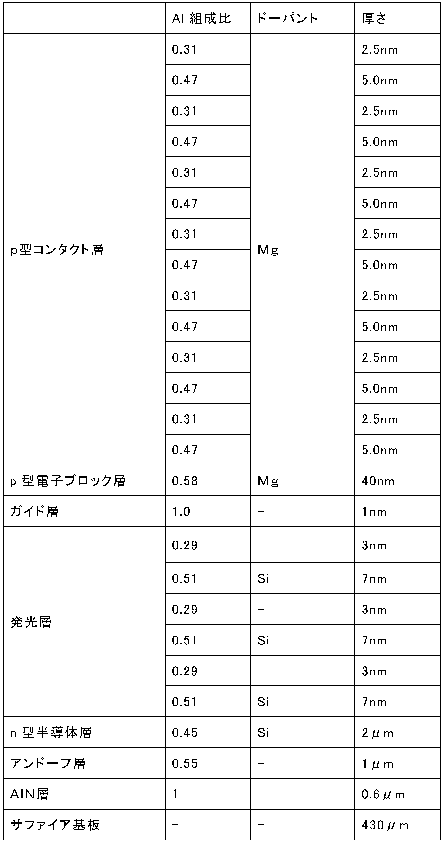
また、露出したn型半導体層上には、Ti/Alからなるn側電極を形成した。Tiの厚さは20nmであり、Alの厚さは150nmである。
最後に、RTA装置(アドバンス理工製;赤外線ランプアニール加熱装置)を用いて最高到達温度550℃に10分間保持して、オーミックコンタクトのための熱処理を行い、NiとRhからなる反射電極を形成した。なお、RTA装置内での熱処理雰囲気は、N2とO2の混合ガスとし、混合ガス中のN2流量を1.0slm,O2流量を0.5slmとした。サファイア基板をレーザースクライブしてチップサイズ1000μm×1000μmに個片化し、実施例1に係る深紫外発光素子を作製した。
実施例1における混合ガス雰囲気に代えて、RTA装置内での熱処理雰囲気をN2ガス(N2流量1.5slm)とした以外は、実施例1と同様にして実施例2に係る深紫外発光素子を作製し評価した。
第1層のAl組成比xを0.43とし、第2層のAl組成yを0.27とした以外は、実施例1と同様にして実施例3に係る深紫外発光素子を作製し評価した。
実施例1における反射電極のNiの厚さを2nmに変えた以外は、実施例1と同様にして、比較例1に係る深紫外発光素子を作製し評価した。
実施例1における反射電極のNiを設けなかった以外は、実施例1と同様にして、比較例2に係る深紫外発光素子を作製し評価した。
実施例1における超格子構造のp型コンタクト層(合計厚さ52.5nm)を、Al0.42Ga0.58N層の厚さ50nmの単層構造に変えた以外は実施例1と同様として、比較例3に係る深紫外発光素子を作製し評価した。
実施例1におけるNiとRhからなる反射電極を、厚さ10nmのNi層と、Ni層上の厚さ20nmのAu層とを順に形成したものに変えた以外は、実施例1と同様にして比較例4に係る深紫外発光素子を作製し発光出力を評価した。
実施例1におけるNiとRhからなる反射電極を、厚さ10nmのNi層と、Ni層上の厚さ20nmのAu層とを順に形成したものに変え、第1層のAl組成比xを0.43とし、第2層のAl組成yを0.27とした以外は、実施例1と同様にして比較例5に係る深紫外発光素子の発光出力を評価した。
実施例1における超格子構造のp型コンタクト層を、AlGaN層の単層構造に替え、そのAl組成比および厚さを表3に記載のとおりとし、反射電極にNiを用いなかった。また、チップサイズを560μm×780μmとした以外は、実施例1と同様にして比較例11~13に係る深紫外発光素子を作製し評価した。
実施例1~3および比較例1~5で得られた発光素子(チップサイズ□1000μm)を、フリップチップ方式で球状Auバンプを用いてAlN製サブマウント(サイズ20mm×15mm、厚さ0.8mm)に実装した。さらにAlN製サブマウントにAl製ヒートシンクを接続した状態で、定電流電源装置を用いて350mAの通電を行い、その際の順方向電圧を測定すると共にサファイア基板側に配置した受光部によりフォトディテクターによる発光出力の測定を行った。結果を表2に示す。なお、スペクトルアナライザによる発光波長の測定を行ったところ、発光中心波長はいずれも310nmであった。値は測定個数10個の平均値である。
実施例および比較例1~5に対して、上記評価1の測定を行った後、350mAを160時間連続通電した。連続通電後に出力を再測定して初期出力と比較し、不点灯あるいは初期の発光出力から半減以下へ出力の急減が有る場合に頓死があったと判定した。測定個数10個のうち、頓死したチップの比率を表2に示す。
比較例11~13については、p型コンタクト層の上にマスクを形成してドライエッチングによるメサエッチングを行い、n型半導体層を露出させたあとの、露出したn型半導体層とp型コンタクト層に対し、サイズ560μm×780μmの小型チップをAuバンプを用いてAlN製サブマウント(サイズ:1.5×1.1mm厚さ:0.2mm)に実装し、20mAを通電した際の発光出力と順方向電厚を測定した。値は測定個数10個の平均値である。さらに、ウェーハ内10か所から抜き取ったチップについて、電流20mAで通電して初期の発光出力を確認し、次いで、電流を20mAで250時間連続通電し、通電後に初期の発光出力から半減以下の出力となる(すなわち、頓死した)チップの比率を表3に示す。なお、発光出力の測定にあたっては、サファイア基板面側に配置したフォトディテクターを用いた。

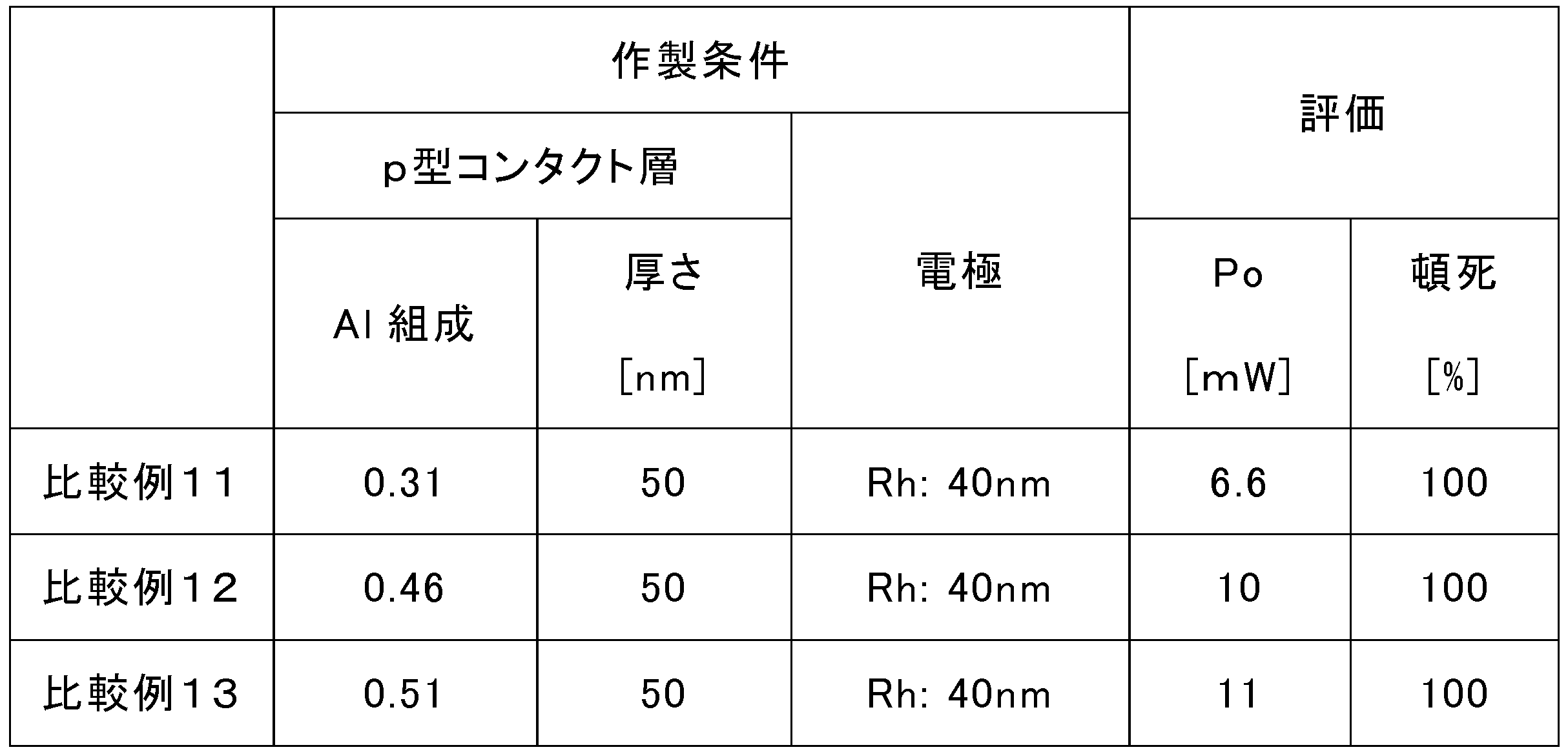
よって、下記[1]と[2]式の条件を同時に満足する。
0.030<z-w0<0.20 ・・・[1]
0.050≦x-y≦0.47 ・・・[2]
比較例1~3で頓死が発生したのは、p型コンタクト層とp側の反射電極界面におけるコンタクト不良が発生したためだと考えられる。一方、実施例1~3では、p型コンタクト層が超格子構造を有し、かつNi層が十分な厚さを有するため、コンタクト不良が発生しなかったと推定される。また、比較例4,5と実施例1~3との比較により、NiとRhからなる反射電極は、順方向電圧を大きく変えることなく発光出力の増大に効果があることが分かる。
実施例1~3では発光中心波長310nmであったところ、これに代えて発光中心波長が280nmとなる深紫外発光素子により実験を行った。実施例1における各半導体層のAl組成比を下記表4に記載のとおりに変えた以外は実施例1と同様にして実施例4に係る深紫外発光素子を作製した。なお、AlNテンプレート基板上のアンドープのAlGaN層は、Al組成比0.85から0.65まで結晶成長方向に組成傾斜させることで形成した。
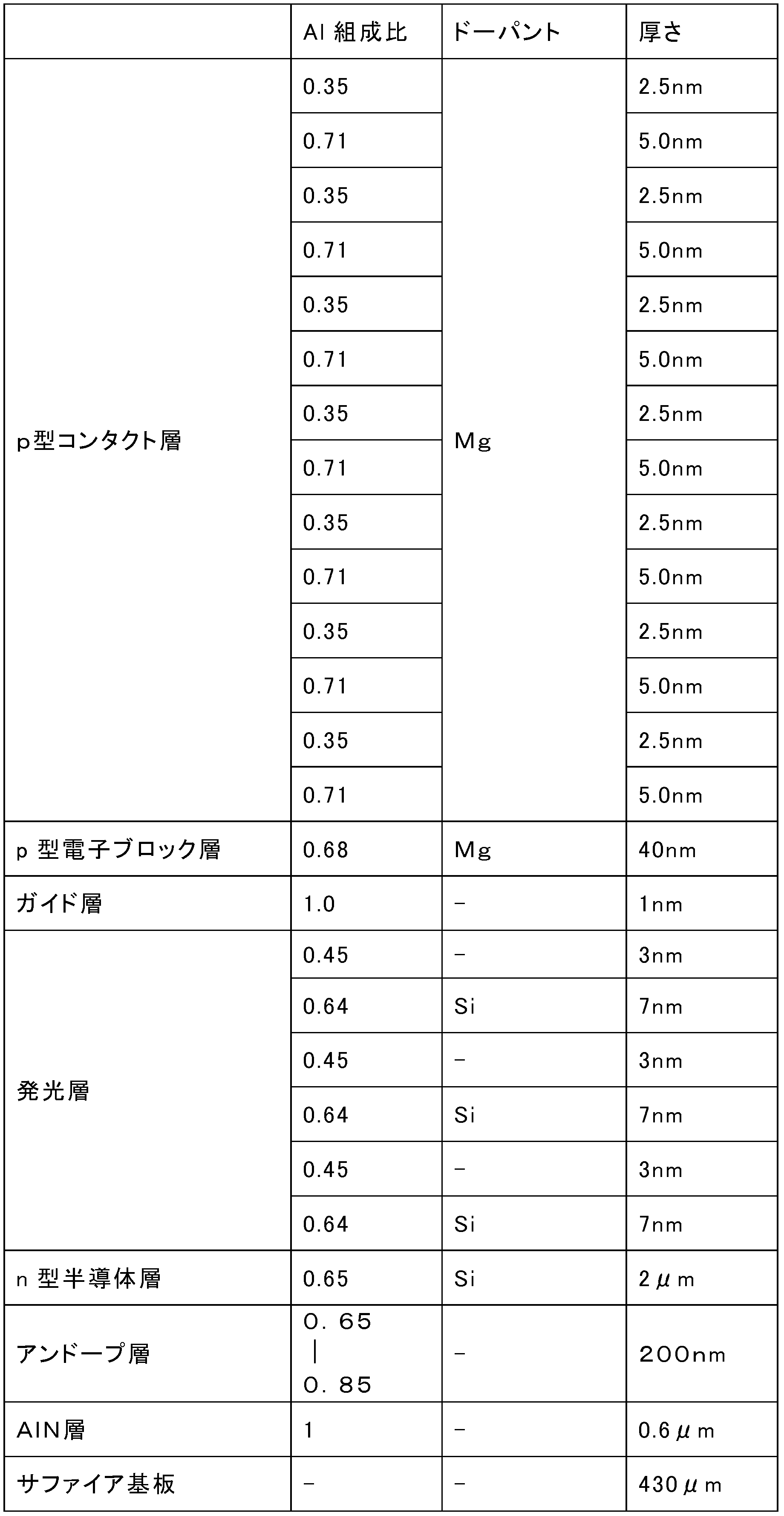
実施例4におけるNiとRhからなる反射電極を、厚さ10nmのNi層と、Ni層上の厚さ20nmのAu層とを順に形成したものに変えた以外は、実施例4と同様にして比較例6に係る深紫外発光素子を作製し発光出力を評価した。
実施例4における超格子構造のp型コンタクト層(合計厚さ52.5nm)を、Al0.59Ga0.41N層の厚さ50nmの単層構造に変えた以外は実施例1と同様として、比較例3に係る深紫外発光素子を作製し評価した。
実施例4および比較例6,7(いずれも実施例1と同様チップサイズ1000μm×1000μm)に対して、上述の評価1と同様にして発光出力Po及び順方向電圧Vfを測定評価した。結果を表5に示す。次いで、この測定を行った後、350mAを20時間連続通電した。連続通電後に出力を再測定して初期出力と比較し、不点灯あるいは初期の発光出力から半減以下へ出力の急減が有る場合に頓死があったと判定した。測定個数10個のうち、頓死したチップの比率を表5に併せて示す。

0.030<z-w0<0.20 ・・・[1]
0.050≦x-y≦0.47 ・・・[2]
比較例7で頓死が発生したのは、比較例3と同様、p型コンタクト層とp側の反射電極界面におけるコンタクト不良が発生したためだと考えられる。一方、実施例4では、p型コンタクト層が超格子構造を有し、かつNi層が十分な厚さを有するため、コンタクト不良が発生しなかったと推定される。また、実施例4と比較例6とを比較すると、NiとRhからなる反射電極は、順方向電圧を大きく変えることなく発光出力の増大に効果があることが分かる。
実施例4と同様にして各半導体層を形成し、次いで、電子ビーム蒸着法を用いて、厚さ7nmのNi層(第1金属層)と、Ni層上の厚さ50nmのRh層(第2金属層)とを順に形成した。続けて、そのRh層(第2金属層)の上に第3金属層として厚さ3nmのNi層を形成し、次いで第4金属層として厚さ20nmのRh層を順に形成した。その後、実施例4と同様に、オーミックコンタクトのための熱処理を行った。その他の作製条件は実施例4と同様である。こうして、実施例5に係る深紫外発光素子を作製した。なお、p型電子ブロック層およびp型コンタクト層のp型層の合計厚さは92.5nmである。
実施例5ではRh層(第2金属層)の上に第3金属層として厚さ3nmのNi層を形成し、次いで第4金属層として厚さ20nmのRh層を順に形成したところ、Rh層(第2金属層)の上に厚さ20nmのAu層を形成した以外は、実施例5と同様にして比較例8に係る深紫外発光素子を作製した。
実施例5ではRh層(第2金属層)の上に第3金属層として厚さ3nmのNi層を形成し、次いで第4金属層として厚さ20nmのRh層を順に形成したところ、Rh層(第2金属層)の上に第3金属層として厚さ3nmのNi層を、第4金属層として厚さ20nmのAu層を順に形成した以外は、実施例5と同様にして比較例9に係る深紫外発光素子を作製した。
評価4では連続通電時間を20時間としていたところ、これを168時間および1000時間に時間を延ばして連続通電した以外は評価4と同様にして、上記の実施例と比較例の頓死の有無を確認した。評価5による評価結果を表6に示す。
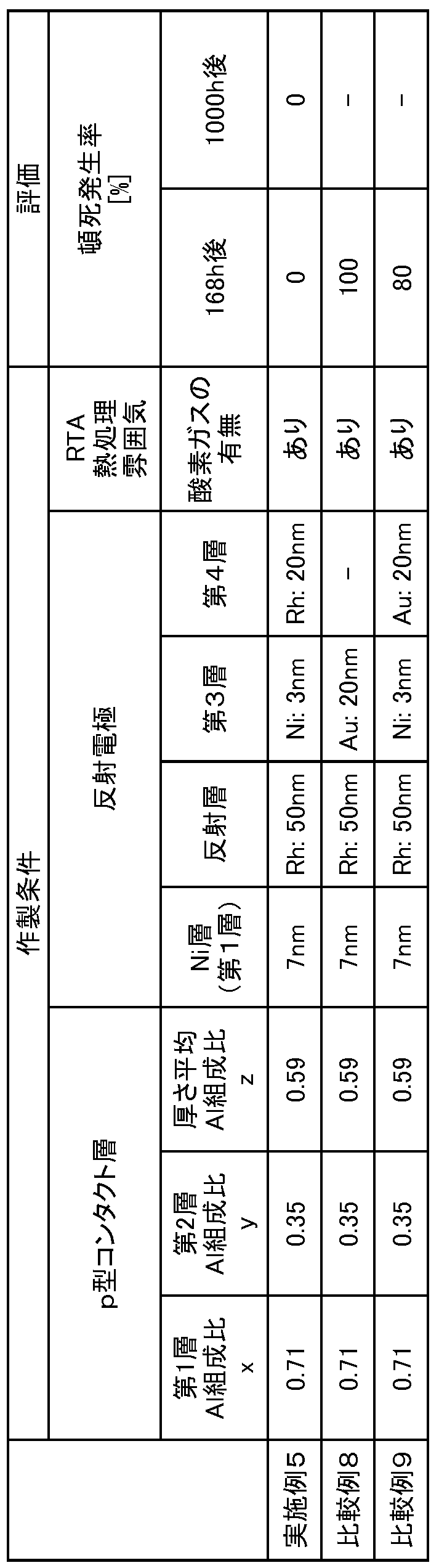
p型電子ブロック層の厚さ40nmから33nmに変更した以外は、実施例5と同様にして実施例6に係る深紫外発光素子を作製し評価した。p型電子ブロック層およびp型コンタクト層のp型層の合計厚さは85.5nmである。
p型コンタクト層の第1層の厚さを5nmから2.5nmへと薄くし、厚さ平均Al組成比zを0.53とした以外は、実施例5と同様にして、実施例7に係る深紫外発光素子を作製し評価した。前記pブロック層および前記p型コンタクト層のp型の合計厚さは75nmである。
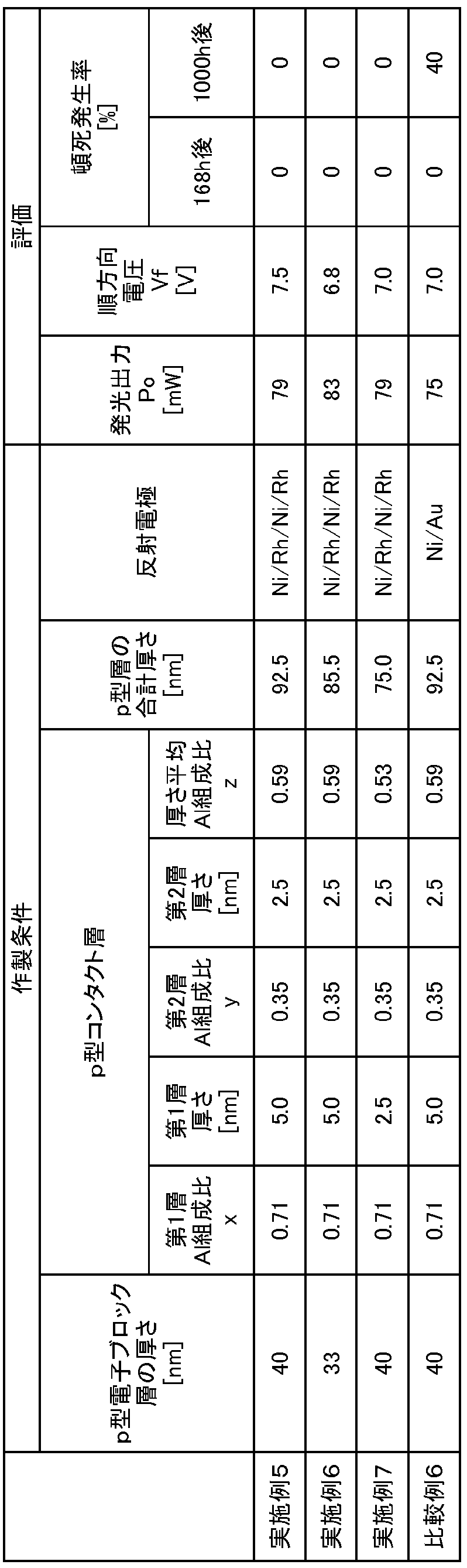
20 バッファ層
30 n型半導体層
40 発光層
41 井戸層
42 障壁層
60 p型電子ブロック層
70 p型コンタクト層
71 第1層
72 第2層
80 反射電極
81 第1金属層
82 第2金属層
83 第3金属層
84 第4金属層
90 n側電極
100 深紫外発光素子
Claims (13)
- 超格子構造を有するp型コンタクト層上に、
第1金属層としてNiを3~20nmの厚さで形成する第1工程と、
前記第1金属層上に第2金属層としてRhを20nm以上2μm以下の厚さで形成する第2工程と、
前記第1金属層及び前記第2金属層に対して300℃以上600℃以下の加熱処理を行う第3工程と、
を具えることを特徴とする深紫外発光素子用の反射電極の製造方法。 - 前記第3工程における加熱処理を行うときの雰囲気ガスが酸素を含む、請求項1に記載の深紫外発光素子用の反射電極の製造方法。
- 前記第2工程の後に、前記第2金属層上に、第3金属層としてNi層を形成する工程と、前記第3金属層上に第4金属層としてRh層を形成する工程をさらに含む、請求項1又は2に記載の深紫外発光素子用の反射電極の製造方法。
- 基板上に、n型半導体層を形成する工程と、
前記n型半導体層上に発光層を形成する工程と、
前記発光層上にp型電子ブロック層を形成する工程と、
前記p型電子ブロック層上にp型コンタクト層を形成する工程と、
前記p型コンタクト層上に反射電極を形成する工程と、
を具える深紫外発光素子の製造方法であって、
前記p型コンタクト層を形成する工程は、Al組成比xを有するAlxGa1-xNからなる第1層を形成する第1工程と、前記Al組成比xよりも低いAl組成比yを有するAlyGa1-yNからなる第2層を形成する第2工程と、を交互に繰り返して超格子構造を有する前記p型コンタクト層を形成し、かつ、前記第2層のAl組成比yが0.15以上であり、
前記反射電極を形成する工程は、
前記p型コンタクト層の最表面の前記第2層上に、
第1金属層としてNiを3~20nmの厚さで形成する第1工程と、
前記第1金属層上に第2金属層としてRhを20nm以上2μm以下の厚さで形成する第2工程と、
前記第1金属層及び前記第2金属層に対して300~600℃の加熱処理を行う第3工程と、
を具えることを特徴とする深紫外発光素子の製造方法。 - 前記p型コンタクト層の超格子構造において、
前記発光層において深紫外光を放出する層のAl組成比をw0としたときに、
前記第1層の前記Al組成比xは前記Al組成比w0よりも高く、
前記第2層の前記Al組成比yは前記Al組成比xよりも低く、
前記Al組成比w0、前記Al組成比x、前記Al組成比y、および前記p型コンタクト層の厚さ平均Al組成比zは下記式[1]、[2]:
0.030<z-w0<0.20 ・・・[1]
0.050≦x-y≦0.47 ・・・[2]
を満足する、請求項4に記載の深紫外発光素子の製造方法。 - 前記発光層における前記p型電子ブロック層に最も近い井戸層と、前記p型電子ブロック層との間に、前記発光層の障壁層及び前記p型電子ブロック層のいずれのAl組成比よりもAl組成比の高いガイド層をさらに有する、請求項5に記載の深紫外発光素子の製造方法。
- 前記ガイド層はAlNからなる、請求項6に記載の深紫外発光素子の製造方法。
- 前記Al組成比w0は、0.25以上0.60以下である、請求項5~7のいずれか1項に記載の深紫外発光素子の製造方法。
- 前記p型電子ブロック層と前記p型コンタクト層とのp型層の合計厚さが、65~100nmである、請求項4~8のいずれか1項に記載の深紫外発光素子の製造方法。
- 前記第2工程の後に、前記第2金属層上に、第3金属層としてNi層を形成する工程と、前記第3金属層上に第4金属層としてRh層を形成する工程をさらに含む、請求項4~9のいずれか1項に記載の深紫外発光素子の製造方法。
- 基板上に、n型半導体層、発光層、p型電子ブロック層およびp型コンタクト層を順次有し、
前記p型コンタクト層は、Al組成比xを有するAlxGa1-xNからなる第1層と、Al組成比yを有するAlyGa1-yNからなる第2層と、を交互に積層してなる超格子構造を有し、かつ、前記第2層の前記Al組成比yが0.15以上であり、
前記p型コンタクト層の最表面の前記第2層上に、NiとRhからなる反射電極を有することを特徴とする深紫外発光素子。 - 前記p型コンタクト層の超格子構造において、
前記発光層において深紫外光を放出する層のAl組成比をw0としたときに、
前記第1層の前記Al組成比xは前記Al組成比w0よりも高く、
前記第2層の前記Al組成比yは前記Al組成比xよりも低く、
前記Al組成比w0、前記Al組成比x、前記Al組成比y、および前記p型コンタクト層の厚さ平均Al組成比zは下記式[1]、[2]:
0.030<z-w0<0.20 ・・・[1]
0.050≦x-y≦0.47 ・・・[2]
を満足する、請求項11に記載の深紫外発光素子 - 前記p型電子ブロック層と前記p型コンタクト層とのp型層の合計厚さが、65~100nmである、請求項11又は12に記載の深紫外発光素子。
Priority Applications (3)
| Application Number | Priority Date | Filing Date | Title |
|---|---|---|---|
| CN202080010391.9A CN113330586B (zh) | 2019-01-22 | 2020-01-20 | 深紫外发光元件用反射电极的制造方法、深紫外发光元件的制造方法及深紫外发光元件 |
| US17/424,562 US12402448B2 (en) | 2019-01-22 | 2020-01-20 | Method of producing reflective electrode for deep ultraviolet light-emitting element, method of producing deep ultraviolet light-emitting element, and deep ultraviolet light-emitting element |
| US19/027,764 US20250176320A1 (en) | 2019-01-22 | 2025-01-17 | Deep ultraviolet light-emitting element |
Applications Claiming Priority (4)
| Application Number | Priority Date | Filing Date | Title |
|---|---|---|---|
| JP2019008785 | 2019-01-22 | ||
| JP2019-008785 | 2019-04-19 | ||
| JP2020006377A JP6793863B2 (ja) | 2019-01-22 | 2020-01-17 | 深紫外発光素子用の反射電極の製造方法、深紫外発光素子の製造方法および深紫外発光素子 |
| JP2020-006377 | 2020-01-17 |
Related Child Applications (2)
| Application Number | Title | Priority Date | Filing Date |
|---|---|---|---|
| US17/424,562 A-371-Of-International US12402448B2 (en) | 2019-01-22 | 2020-01-20 | Method of producing reflective electrode for deep ultraviolet light-emitting element, method of producing deep ultraviolet light-emitting element, and deep ultraviolet light-emitting element |
| US19/027,764 Continuation US20250176320A1 (en) | 2019-01-22 | 2025-01-17 | Deep ultraviolet light-emitting element |
Publications (1)
| Publication Number | Publication Date |
|---|---|
| WO2020153308A1 true WO2020153308A1 (ja) | 2020-07-30 |
Family
ID=71736648
Family Applications (1)
| Application Number | Title | Priority Date | Filing Date |
|---|---|---|---|
| PCT/JP2020/001761 Ceased WO2020153308A1 (ja) | 2019-01-22 | 2020-01-20 | 深紫外発光素子用の反射電極の製造方法、深紫外発光素子の製造方法および深紫外発光素子 |
Country Status (3)
| Country | Link |
|---|---|
| US (2) | US12402448B2 (ja) |
| JP (1) | JP7623794B2 (ja) |
| WO (1) | WO2020153308A1 (ja) |
Cited By (2)
| Publication number | Priority date | Publication date | Assignee | Title |
|---|---|---|---|---|
| CN112420887A (zh) * | 2020-11-20 | 2021-02-26 | 广东省科学院半导体研究所 | 一种深紫外led器件及其制作方法 |
| JP2022172792A (ja) * | 2021-05-07 | 2022-11-17 | 日機装株式会社 | 窒化物半導体発光素子 |
Citations (5)
| Publication number | Priority date | Publication date | Assignee | Title |
|---|---|---|---|---|
| JP2002280610A (ja) * | 2001-03-21 | 2002-09-27 | Nippon Telegr & Teleph Corp <Ntt> | 紫外発光ダイオード |
| JP2012182211A (ja) * | 2011-02-28 | 2012-09-20 | Toshiba Corp | 半導体発光素子及び半導体発光装置 |
| JP2012248765A (ja) * | 2011-05-30 | 2012-12-13 | Showa Denko Kk | Iii族窒化物半導体発光素子の製造方法 |
| WO2017017891A1 (ja) * | 2015-07-30 | 2017-02-02 | Dowaエレクトロニクス株式会社 | Iii族窒化物半導体発光素子およびその製造方法 |
| WO2018181044A1 (ja) * | 2017-03-27 | 2018-10-04 | Dowaエレクトロニクス株式会社 | Iii族窒化物半導体発光素子およびその製造方法 |
Family Cites Families (23)
| Publication number | Priority date | Publication date | Assignee | Title |
|---|---|---|---|---|
| JP3736181B2 (ja) | 1998-05-13 | 2006-01-18 | 豊田合成株式会社 | Iii族窒化物系化合物半導体発光素子 |
| JP4034015B2 (ja) * | 1999-09-01 | 2008-01-16 | 豊田合成株式会社 | Iii族窒化物系化合物半導体発光素子 |
| JP2004281553A (ja) | 2003-03-13 | 2004-10-07 | Nippon Telegr & Teleph Corp <Ntt> | 発光ダイオード |
| KR100576872B1 (ko) * | 2004-09-17 | 2006-05-10 | 삼성전기주식회사 | 정전기 방전 방지기능을 갖는 질화물 반도체 발광소자 |
| US7501295B2 (en) | 2006-05-25 | 2009-03-10 | Philips Lumileds Lighting Company, Llc | Method of fabricating a reflective electrode for a semiconductor light emitting device |
| KR100975659B1 (ko) * | 2007-12-18 | 2010-08-17 | 포항공과대학교 산학협력단 | 발광 소자 및 그 제조 방법 |
| TWI412159B (zh) * | 2008-06-16 | 2013-10-11 | 豐田合成股份有限公司 | 半導體發光元件、其電極以及製造方法、及燈 |
| KR101055090B1 (ko) | 2009-03-02 | 2011-08-08 | 엘지이노텍 주식회사 | 반도체 발광소자 및 그 제조방법 |
| TW201140880A (en) | 2009-12-24 | 2011-11-16 | Dowa Electronics Materials Co Ltd | Vertical group iii nitride semiconductor light-emitting element and production method therefor |
| JP2012094630A (ja) * | 2010-10-26 | 2012-05-17 | Toshiba Corp | 半導体発光素子 |
| US8787418B2 (en) * | 2011-08-11 | 2014-07-22 | Sensor Electronic Technology, Inc. | Emitting device with compositional and doping inhomogeneities in semiconductor layers |
| US9252329B2 (en) * | 2011-10-04 | 2016-02-02 | Palo Alto Research Center Incorporated | Ultraviolet light emitting devices having compressively strained light emitting layer for enhanced light extraction |
| TWI467807B (zh) | 2011-10-28 | 2015-01-01 | Rgb Consulting Co Ltd | 覆晶式之發光二極體 |
| TWI606618B (zh) * | 2012-01-03 | 2017-11-21 | Lg伊諾特股份有限公司 | 發光裝置 |
| US9059356B1 (en) * | 2013-11-22 | 2015-06-16 | Sandia Corporation | Laterally injected light-emitting diode and laser diode |
| JP2015216352A (ja) | 2014-04-24 | 2015-12-03 | 国立研究開発法人理化学研究所 | 紫外発光ダイオードおよびそれを備える電気機器 |
| JP6001756B2 (ja) * | 2014-12-08 | 2016-10-05 | Dowaエレクトロニクス株式会社 | Iii族窒化物半導体発光素子の製造方法およびiii族窒化物半導体発光素子 |
| TWI681570B (zh) | 2015-02-06 | 2020-01-01 | 日商斯坦雷電氣股份有限公司 | 發光元件及發光元件之製造方法 |
| US9859461B2 (en) * | 2015-07-13 | 2018-01-02 | Sensor Electronic Technology, Inc. | P-type contact to semiconductor heterostructure |
| US10236415B2 (en) * | 2015-07-13 | 2019-03-19 | Sensor Electronic Technology, Inc. | P-type contact to semiconductor heterostructure |
| US10790410B2 (en) | 2015-10-23 | 2020-09-29 | Sensor Electronic Technology, Inc. | Light extraction from optoelectronic device |
| CN106328781B (zh) | 2016-11-03 | 2018-12-11 | 湘能华磊光电股份有限公司 | 高反射率led电极及其制备方法 |
| US11063178B2 (en) * | 2017-10-25 | 2021-07-13 | Sensor Electronic Technology, Inc. | Semiconductor heterostructure with improved light emission |
-
2020
- 2020-01-20 US US17/424,562 patent/US12402448B2/en active Active
- 2020-01-20 WO PCT/JP2020/001761 patent/WO2020153308A1/ja not_active Ceased
- 2020-05-22 JP JP2020090012A patent/JP7623794B2/ja active Active
-
2025
- 2025-01-17 US US19/027,764 patent/US20250176320A1/en active Pending
Patent Citations (5)
| Publication number | Priority date | Publication date | Assignee | Title |
|---|---|---|---|---|
| JP2002280610A (ja) * | 2001-03-21 | 2002-09-27 | Nippon Telegr & Teleph Corp <Ntt> | 紫外発光ダイオード |
| JP2012182211A (ja) * | 2011-02-28 | 2012-09-20 | Toshiba Corp | 半導体発光素子及び半導体発光装置 |
| JP2012248765A (ja) * | 2011-05-30 | 2012-12-13 | Showa Denko Kk | Iii族窒化物半導体発光素子の製造方法 |
| WO2017017891A1 (ja) * | 2015-07-30 | 2017-02-02 | Dowaエレクトロニクス株式会社 | Iii族窒化物半導体発光素子およびその製造方法 |
| WO2018181044A1 (ja) * | 2017-03-27 | 2018-10-04 | Dowaエレクトロニクス株式会社 | Iii族窒化物半導体発光素子およびその製造方法 |
Non-Patent Citations (2)
| Title |
|---|
| JEONG-WOO PARK, SONG JUNE-O, LEEM DONG-SEOK, SEONG TAE-YEON: "Low-Resistance and Reflective Ni/Rh and Ni/Au/Rh Contacts to p-GaN for Flip-Chil LEDs", ELECTROCHEMICAL AND SOLID-STATE LETTERS, vol. 8, no. 1, 29 November 2004 (2004-11-29), pages 1 - 4, XP055727665, ISSN: 1099-0062, DOI: 10.1149/1.1830391 * |
| TAKAYOSHI TAKANO; TAKUYA MINO; JUN SAKAI; NORIMICHI NOGUCHI; KENJI TSUBAKI; HIDEKI HIRAYAMA: "Deep-ultraviolet light-emitting diodes with external quantum efficiency higher than 20% at 275 nm achieved by improving light-extraction efficiency", APPLIED PHYSICS EXPRESS, vol. 10, no. 3, 14 February 2017 (2017-02-14), pages 4, XP055611295, ISSN: 1882-0778, DOI: 10.7567/APEX.10.031002 * |
Cited By (2)
| Publication number | Priority date | Publication date | Assignee | Title |
|---|---|---|---|---|
| CN112420887A (zh) * | 2020-11-20 | 2021-02-26 | 广东省科学院半导体研究所 | 一种深紫外led器件及其制作方法 |
| JP2022172792A (ja) * | 2021-05-07 | 2022-11-17 | 日機装株式会社 | 窒化物半導体発光素子 |
Also Published As
| Publication number | Publication date |
|---|---|
| US20220123177A1 (en) | 2022-04-21 |
| JP7623794B2 (ja) | 2025-01-29 |
| US20250176320A1 (en) | 2025-05-29 |
| JP2020129697A (ja) | 2020-08-27 |
| US12402448B2 (en) | 2025-08-26 |
Similar Documents
| Publication | Publication Date | Title |
|---|---|---|
| CN111164768B (zh) | 深紫外发光元件及其制造方法 | |
| CN110462851B (zh) | Iii族氮化物半导体发光元件及其制造方法 | |
| JP3920315B2 (ja) | 窒化物系半導体発光素子 | |
| JP6940664B2 (ja) | 深紫外発光素子およびその製造方法 | |
| CN113169255B (zh) | Iii族氮化物半导体发光元件及其制造方法 | |
| CN100448041C (zh) | 半导体发光元件 | |
| JP2024177256A (ja) | 深紫外発光素子 | |
| US6734091B2 (en) | Electrode for p-type gallium nitride-based semiconductors | |
| US20250176320A1 (en) | Deep ultraviolet light-emitting element | |
| TWI299915B (en) | Group iii nitride semiconductor light-emitting device | |
| WO2020122137A1 (ja) | Iii族窒化物半導体発光素子及びその製造方法 | |
| JPWO2008153065A1 (ja) | 半導体発光素子及びその製造方法 |
Legal Events
| Date | Code | Title | Description |
|---|---|---|---|
| 121 | Ep: the epo has been informed by wipo that ep was designated in this application |
Ref document number: 20744822 Country of ref document: EP Kind code of ref document: A1 |
|
| NENP | Non-entry into the national phase |
Ref country code: DE |
|
| 122 | Ep: pct application non-entry in european phase |
Ref document number: 20744822 Country of ref document: EP Kind code of ref document: A1 |
|
| WWG | Wipo information: grant in national office |
Ref document number: 202080010391.9 Country of ref document: CN |
|
| WWG | Wipo information: grant in national office |
Ref document number: 17424562 Country of ref document: US |