WO2020152947A1 - 直流パルス電源装置 - Google Patents
直流パルス電源装置 Download PDFInfo
- Publication number
- WO2020152947A1 WO2020152947A1 PCT/JP2019/043836 JP2019043836W WO2020152947A1 WO 2020152947 A1 WO2020152947 A1 WO 2020152947A1 JP 2019043836 W JP2019043836 W JP 2019043836W WO 2020152947 A1 WO2020152947 A1 WO 2020152947A1
- Authority
- WO
- WIPO (PCT)
- Prior art keywords
- voltage
- reactor
- unit
- power supply
- pulse
- Prior art date
- Legal status (The legal status is an assumption and is not a legal conclusion. Google has not performed a legal analysis and makes no representation as to the accuracy of the status listed.)
- Ceased
Links
Images


Classifications
-
- H—ELECTRICITY
- H02—GENERATION; CONVERSION OR DISTRIBUTION OF ELECTRIC POWER
- H02M—APPARATUS FOR CONVERSION BETWEEN AC AND AC, BETWEEN AC AND DC, OR BETWEEN DC AND DC, AND FOR USE WITH MAINS OR SIMILAR POWER SUPPLY SYSTEMS; CONVERSION OF DC OR AC INPUT POWER INTO SURGE OUTPUT POWER; CONTROL OR REGULATION THEREOF
- H02M1/00—Details of apparatus for conversion
- H02M1/0067—Converter structures employing plural converter units, other than for parallel operation of the units on a single load
- H02M1/007—Plural converter units in cascade
-
- H—ELECTRICITY
- H02—GENERATION; CONVERSION OR DISTRIBUTION OF ELECTRIC POWER
- H02M—APPARATUS FOR CONVERSION BETWEEN AC AND AC, BETWEEN AC AND DC, OR BETWEEN DC AND DC, AND FOR USE WITH MAINS OR SIMILAR POWER SUPPLY SYSTEMS; CONVERSION OF DC OR AC INPUT POWER INTO SURGE OUTPUT POWER; CONTROL OR REGULATION THEREOF
- H02M3/00—Conversion of DC power input into DC power output
- H02M3/02—Conversion of DC power input into DC power output without intermediate conversion into AC
- H02M3/04—Conversion of DC power input into DC power output without intermediate conversion into AC by static converters
- H02M3/10—Conversion of DC power input into DC power output without intermediate conversion into AC by static converters using discharge tubes with control electrode or semiconductor devices with control electrode
- H02M3/145—Conversion of DC power input into DC power output without intermediate conversion into AC by static converters using discharge tubes with control electrode or semiconductor devices with control electrode using devices of a triode or transistor type requiring continuous application of a control signal
- H02M3/155—Conversion of DC power input into DC power output without intermediate conversion into AC by static converters using discharge tubes with control electrode or semiconductor devices with control electrode using devices of a triode or transistor type requiring continuous application of a control signal using semiconductor devices only
- H02M3/156—Conversion of DC power input into DC power output without intermediate conversion into AC by static converters using discharge tubes with control electrode or semiconductor devices with control electrode using devices of a triode or transistor type requiring continuous application of a control signal using semiconductor devices only with automatic control of output voltage or current, e.g. switching regulators
- H02M3/158—Conversion of DC power input into DC power output without intermediate conversion into AC by static converters using discharge tubes with control electrode or semiconductor devices with control electrode using devices of a triode or transistor type requiring continuous application of a control signal using semiconductor devices only with automatic control of output voltage or current, e.g. switching regulators including plural semiconductor devices as final control devices for a single load
-
- H—ELECTRICITY
- H02—GENERATION; CONVERSION OR DISTRIBUTION OF ELECTRIC POWER
- H02M—APPARATUS FOR CONVERSION BETWEEN AC AND AC, BETWEEN AC AND DC, OR BETWEEN DC AND DC, AND FOR USE WITH MAINS OR SIMILAR POWER SUPPLY SYSTEMS; CONVERSION OF DC OR AC INPUT POWER INTO SURGE OUTPUT POWER; CONTROL OR REGULATION THEREOF
- H02M3/00—Conversion of DC power input into DC power output
- H02M3/02—Conversion of DC power input into DC power output without intermediate conversion into AC
- H02M3/04—Conversion of DC power input into DC power output without intermediate conversion into AC by static converters
- H02M3/10—Conversion of DC power input into DC power output without intermediate conversion into AC by static converters using discharge tubes with control electrode or semiconductor devices with control electrode
- H02M3/145—Conversion of DC power input into DC power output without intermediate conversion into AC by static converters using discharge tubes with control electrode or semiconductor devices with control electrode using devices of a triode or transistor type requiring continuous application of a control signal
- H02M3/155—Conversion of DC power input into DC power output without intermediate conversion into AC by static converters using discharge tubes with control electrode or semiconductor devices with control electrode using devices of a triode or transistor type requiring continuous application of a control signal using semiconductor devices only
-
- H—ELECTRICITY
- H01—ELECTRIC ELEMENTS
- H01J—ELECTRIC DISCHARGE TUBES OR DISCHARGE LAMPS
- H01J37/00—Discharge tubes with provision for introducing objects or material to be exposed to the discharge, e.g. for the purpose of examination or processing thereof
- H01J37/32—Gas-filled discharge tubes
- H01J37/32009—Arrangements for generation of plasma specially adapted for examination or treatment of objects, e.g. plasma sources
- H01J37/32018—Glow discharge
- H01J37/32027—DC powered
-
- H—ELECTRICITY
- H02—GENERATION; CONVERSION OR DISTRIBUTION OF ELECTRIC POWER
- H02M—APPARATUS FOR CONVERSION BETWEEN AC AND AC, BETWEEN AC AND DC, OR BETWEEN DC AND DC, AND FOR USE WITH MAINS OR SIMILAR POWER SUPPLY SYSTEMS; CONVERSION OF DC OR AC INPUT POWER INTO SURGE OUTPUT POWER; CONTROL OR REGULATION THEREOF
- H02M1/00—Details of apparatus for conversion
- H02M1/0064—Magnetic structures combining different functions, e.g. storage, filtering or transformation
-
- H—ELECTRICITY
- H02—GENERATION; CONVERSION OR DISTRIBUTION OF ELECTRIC POWER
- H02M—APPARATUS FOR CONVERSION BETWEEN AC AND AC, BETWEEN AC AND DC, OR BETWEEN DC AND DC, AND FOR USE WITH MAINS OR SIMILAR POWER SUPPLY SYSTEMS; CONVERSION OF DC OR AC INPUT POWER INTO SURGE OUTPUT POWER; CONTROL OR REGULATION THEREOF
- H02M1/00—Details of apparatus for conversion
- H02M1/32—Means for protecting converters other than automatic disconnection
- H02M1/34—Snubber circuits
- H02M1/342—Active non-dissipative snubbers
-
- H—ELECTRICITY
- H02—GENERATION; CONVERSION OR DISTRIBUTION OF ELECTRIC POWER
- H02M—APPARATUS FOR CONVERSION BETWEEN AC AND AC, BETWEEN AC AND DC, OR BETWEEN DC AND DC, AND FOR USE WITH MAINS OR SIMILAR POWER SUPPLY SYSTEMS; CONVERSION OF DC OR AC INPUT POWER INTO SURGE OUTPUT POWER; CONTROL OR REGULATION THEREOF
- H02M3/00—Conversion of DC power input into DC power output
- H02M3/22—Conversion of DC power input into DC power output with intermediate conversion into AC
- H02M3/24—Conversion of DC power input into DC power output with intermediate conversion into AC by static converters
- H02M3/28—Conversion of DC power input into DC power output with intermediate conversion into AC by static converters using discharge tubes with control electrode or semiconductor devices with control electrode to produce the intermediate AC
- H02M3/325—Conversion of DC power input into DC power output with intermediate conversion into AC by static converters using discharge tubes with control electrode or semiconductor devices with control electrode to produce the intermediate AC using devices of a triode or a transistor type requiring continuous application of a control signal
- H02M3/335—Conversion of DC power input into DC power output with intermediate conversion into AC by static converters using discharge tubes with control electrode or semiconductor devices with control electrode to produce the intermediate AC using devices of a triode or a transistor type requiring continuous application of a control signal using semiconductor devices only
- H02M3/33507—Conversion of DC power input into DC power output with intermediate conversion into AC by static converters using discharge tubes with control electrode or semiconductor devices with control electrode to produce the intermediate AC using devices of a triode or a transistor type requiring continuous application of a control signal using semiconductor devices only with automatic control of the output voltage or current, e.g. flyback converters
-
- H—ELECTRICITY
- H02—GENERATION; CONVERSION OR DISTRIBUTION OF ELECTRIC POWER
- H02M—APPARATUS FOR CONVERSION BETWEEN AC AND AC, BETWEEN AC AND DC, OR BETWEEN DC AND DC, AND FOR USE WITH MAINS OR SIMILAR POWER SUPPLY SYSTEMS; CONVERSION OF DC OR AC INPUT POWER INTO SURGE OUTPUT POWER; CONTROL OR REGULATION THEREOF
- H02M3/00—Conversion of DC power input into DC power output
- H02M3/22—Conversion of DC power input into DC power output with intermediate conversion into AC
- H02M3/24—Conversion of DC power input into DC power output with intermediate conversion into AC by static converters
- H02M3/28—Conversion of DC power input into DC power output with intermediate conversion into AC by static converters using discharge tubes with control electrode or semiconductor devices with control electrode to produce the intermediate AC
- H02M3/325—Conversion of DC power input into DC power output with intermediate conversion into AC by static converters using discharge tubes with control electrode or semiconductor devices with control electrode to produce the intermediate AC using devices of a triode or a transistor type requiring continuous application of a control signal
- H02M3/335—Conversion of DC power input into DC power output with intermediate conversion into AC by static converters using discharge tubes with control electrode or semiconductor devices with control electrode to produce the intermediate AC using devices of a triode or a transistor type requiring continuous application of a control signal using semiconductor devices only
- H02M3/33569—Conversion of DC power input into DC power output with intermediate conversion into AC by static converters using discharge tubes with control electrode or semiconductor devices with control electrode to produce the intermediate AC using devices of a triode or a transistor type requiring continuous application of a control signal using semiconductor devices only having several active switching elements
- H02M3/33573—Full-bridge at primary side of an isolation transformer
-
- H—ELECTRICITY
- H02—GENERATION; CONVERSION OR DISTRIBUTION OF ELECTRIC POWER
- H02M—APPARATUS FOR CONVERSION BETWEEN AC AND AC, BETWEEN AC AND DC, OR BETWEEN DC AND DC, AND FOR USE WITH MAINS OR SIMILAR POWER SUPPLY SYSTEMS; CONVERSION OF DC OR AC INPUT POWER INTO SURGE OUTPUT POWER; CONTROL OR REGULATION THEREOF
- H02M7/00—Conversion of AC power input into DC power output; Conversion of DC power input into AC power output
- H02M7/42—Conversion of DC power input into AC power output without possibility of reversal
- H02M7/44—Conversion of DC power input into AC power output without possibility of reversal by static converters
- H02M7/48—Conversion of DC power input into AC power output without possibility of reversal by static converters using discharge tubes with control electrode or semiconductor devices with control electrode
- H02M7/53—Conversion of DC power input into AC power output without possibility of reversal by static converters using discharge tubes with control electrode or semiconductor devices with control electrode using devices of a triode or transistor type requiring continuous application of a control signal
- H02M7/537—Conversion of DC power input into AC power output without possibility of reversal by static converters using discharge tubes with control electrode or semiconductor devices with control electrode using devices of a triode or transistor type requiring continuous application of a control signal using semiconductor devices only, e.g. single switched pulse inverters
- H02M7/5387—Conversion of DC power input into AC power output without possibility of reversal by static converters using discharge tubes with control electrode or semiconductor devices with control electrode using devices of a triode or transistor type requiring continuous application of a control signal using semiconductor devices only, e.g. single switched pulse inverters in a bridge configuration
-
- H—ELECTRICITY
- H02—GENERATION; CONVERSION OR DISTRIBUTION OF ELECTRIC POWER
- H02M—APPARATUS FOR CONVERSION BETWEEN AC AND AC, BETWEEN AC AND DC, OR BETWEEN DC AND DC, AND FOR USE WITH MAINS OR SIMILAR POWER SUPPLY SYSTEMS; CONVERSION OF DC OR AC INPUT POWER INTO SURGE OUTPUT POWER; CONTROL OR REGULATION THEREOF
- H02M1/00—Details of apparatus for conversion
- H02M1/0003—Details of control, feedback or regulation circuits
- H02M1/0009—Devices or circuits for detecting current in a converter
-
- H—ELECTRICITY
- H02—GENERATION; CONVERSION OR DISTRIBUTION OF ELECTRIC POWER
- H02M—APPARATUS FOR CONVERSION BETWEEN AC AND AC, BETWEEN AC AND DC, OR BETWEEN DC AND DC, AND FOR USE WITH MAINS OR SIMILAR POWER SUPPLY SYSTEMS; CONVERSION OF DC OR AC INPUT POWER INTO SURGE OUTPUT POWER; CONTROL OR REGULATION THEREOF
- H02M1/00—Details of apparatus for conversion
- H02M1/0067—Converter structures employing plural converter units, other than for parallel operation of the units on a single load
- H02M1/0077—Plural converter units whose outputs are connected in series
-
- H—ELECTRICITY
- H02—GENERATION; CONVERSION OR DISTRIBUTION OF ELECTRIC POWER
- H02M—APPARATUS FOR CONVERSION BETWEEN AC AND AC, BETWEEN AC AND DC, OR BETWEEN DC AND DC, AND FOR USE WITH MAINS OR SIMILAR POWER SUPPLY SYSTEMS; CONVERSION OF DC OR AC INPUT POWER INTO SURGE OUTPUT POWER; CONTROL OR REGULATION THEREOF
- H02M7/00—Conversion of AC power input into DC power output; Conversion of DC power input into AC power output
- H02M7/02—Conversion of AC power input into DC power output without possibility of reversal
- H02M7/04—Conversion of AC power input into DC power output without possibility of reversal by static converters
- H02M7/06—Conversion of AC power input into DC power output without possibility of reversal by static converters using discharge tubes without control electrode or semiconductor devices without control electrode
-
- Y—GENERAL TAGGING OF NEW TECHNOLOGICAL DEVELOPMENTS; GENERAL TAGGING OF CROSS-SECTIONAL TECHNOLOGIES SPANNING OVER SEVERAL SECTIONS OF THE IPC; TECHNICAL SUBJECTS COVERED BY FORMER USPC CROSS-REFERENCE ART COLLECTIONS [XRACs] AND DIGESTS
- Y02—TECHNOLOGIES OR APPLICATIONS FOR MITIGATION OR ADAPTATION AGAINST CLIMATE CHANGE
- Y02B—CLIMATE CHANGE MITIGATION TECHNOLOGIES RELATED TO BUILDINGS, e.g. HOUSING, HOUSE APPLIANCES OR RELATED END-USER APPLICATIONS
- Y02B70/00—Technologies for an efficient end-user side electric power management and consumption
- Y02B70/10—Technologies improving the efficiency by using switched-mode power supplies [SMPS], i.e. efficient power electronics conversion e.g. power factor correction or reduction of losses in power supplies or efficient standby modes
Definitions
- the present invention relates to a DC pulse power supply device that supplies a pulse output to a load.
- the pulse output output from the DC pulse power supply is a high-frequency output that repeats the on and off states of the DC voltage at several Hz to several hundred kHz.
- DC pulse power supply is used as a power supply that supplies pulse output to loads such as plasma generator, pulse laser excitation, and electric discharge machine.
- loads such as plasma generator, pulse laser excitation, and electric discharge machine.
- the DC power supply device is used as a plasma generation device, a pulse output is supplied between the electrodes in the plasma generation chamber to ignite the plasma due to the discharge between the electrodes and maintain the generated plasma.
- FIG. 9A shows an example of the configuration of the DC pulse power supply device.
- a DC pulse power supply device includes a boost chopper circuit as a circuit that generates a pulse waveform.
- the DC pulse power supply device 100 includes a DC power supply 110 and a boost chopper circuit 120, and supplies a pulse output obtained by boosting the DC voltage of the DC power supply 110 by the boost chopper circuit 120 to a load 130 (Patent Documents 1 and 2).
- FIG. 9B shows a configuration example of the boost chopper circuit (Patent Document 3).
- the step-up chopper circuit 120 is configured by connecting an inductor 121 in series between a DC power supply side and a load side, and connecting a switching element 122 in parallel to the load side. A pulsed output that is boosted according to the ratio is formed. In this on/off operation, energy corresponding to the time width of the on period is accumulated in the DC reactor of the inductor 121, and a pulse output having an amplitude boosted according to the accumulated energy is formed.
- the amplitude of the pulse output to be boosted is determined by the duty ratio of the ON/OFF period of the switching element, but the amplitude may exceed the set amplitude due to vibration or the like generated when the switching element 122 is OFF.
- a step-up chopper circuit including a series circuit of a reactor and a switching element, a series circuit of a reactor Lr, a diode D1 and a capacitor C1 is connected to both ends of a switching element Q1, and a switching element Q2 constituting an active clamp circuit is connected to both ends of the reactor Lr.
- a configuration is known in which a series circuit of a capacitor C2 is connected and the switching element Q1 of the boost chopper circuit is subjected to zero voltage switching (ZVS) by an active clamp circuit (Patent Document 4).
- JP-A-8-222258 (FIG. 1, paragraph 0012) Japanese Patent Laid-Open No. 2006-6053 (FIG. 1) Japanese Unexamined Patent Publication No. 1-252165 (FIG. 1) Japanese Unexamined Patent Publication No. 2012-178952 (FIGS. 1 and 9)
- the pulse output of the step-up chopper circuit determines the boosted amplitude depending on the duty ratio of the on/off period of the switching element. Therefore, it is necessary to increase the duty ratio to increase the output voltage of the pulse output. Needs to shorten the time width of the off period.
- the present invention aims to solve the above-mentioned conventional problems and increase the output voltage of the pulse output of the step-up chopper circuit in the DC pulse power supply device.
- the DC pulse power supply device of the present invention increases the output voltage of the pulse output of the boost chopper circuit by superimposing the regenerative voltage and/or the reactor voltage on the pulse output of the boost chopper circuit.
- the DC pulse power supply device of the present invention includes a DC power supply, a pulse unit that generates a pulse output by a boost chopper circuit connected to the DC power supply, and a voltage superposition unit connected to the DC reactor of the boost chopper circuit.
- the voltage superimposing unit superimposes the superimposed voltage component on the output voltage of the boost chopper circuit to raise the voltage.
- the pulse unit outputs a pulse of the output voltage on which the superimposed voltage component is superimposed by the voltage superimposing unit.
- the voltage superposition unit has multiple forms.
- the voltage superimposing unit of the first mode is a regenerative voltage unit, and the voltage superimposing unit of the second mode is a reactor voltage unit.
- the voltage superimposing unit of the first form can be configured using a regenerative unit.
- the regenerative unit clamps the output voltage of the boost chopper circuit to a set voltage, superimposes the regenerative voltage of the clamp voltage as a superimposed voltage component on the DC reactor of the boost chopper circuit, and regenerates a voltage exceeding the set voltage to the DC power supply.
- the reactor voltage section of the second form superimposes the reactor voltage of the induced voltage induced in the second DC reactor by magnetic coupling with the DC reactor forming the boost chopper circuit as the superimposed voltage component.
- the DC power supply device of the present invention includes, as a voltage superimposing unit, a configuration including the regenerative voltage unit of the first mode, a configuration including a reactor voltage unit of the second mode, and the regenerative voltage unit of the first mode and the first mode.
- the configuration of the third aspect may be provided with two voltage superimposing sections of the reactor voltage section of the second aspect.
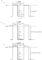
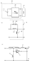
- FIG. 1 is a diagram for explaining a schematic configuration of a pulse unit and a voltage superimposing unit included in the DC pulse power supply device of the present invention
- FIG. 1A includes a regenerative voltage unit as a first form of the voltage superimposing unit
- 1B shows a configuration including a reactor voltage unit as a second form of the voltage superimposing unit
- FIG. 1C shows a regenerative voltage unit and a reactor as a third form of the voltage superimposing unit. The structure provided with the voltage part is shown.
- the pulse unit 20 includes a step-up chopper circuit composed of a series circuit of a DC reactor 21 and a switching element 22, and as the voltage superimposing unit of the first embodiment, the output voltage of the pulse output of the pulse unit 20 is a regenerative voltage.
- a regenerative voltage unit 30A for superimposing The regenerative voltage unit 30A is connected in parallel between both ends of the DC reactor 21, and applies the reactor voltage V DCL of the DC reactor 21 to the capacitor voltage Vc.
- the output voltage Vo of the pulse output of the pulse unit 20 becomes (VAB+Vc) in which the capacitor voltage Vc is superimposed on the DC voltage VAB of the DC power supply.
- the regenerative voltage unit 30A can be configured such that the regenerative unit is connected in parallel between both ends of the DC reactor 21 of the boost chopper circuit.
- the regenerative unit regenerates a voltage of the reactor voltage of the DC reactor 21 that exceeds the set voltage to the DC power supply.
- the regenerative unit forms a clamp circuit that uses a charging voltage of a capacitor connected in parallel at both ends of the DC reactor as a clamp voltage, and regenerates a voltage exceeding the clamp voltage to a DC power supply.
- the regenerative voltage unit 30A superimposes the regenerative voltage of the set voltage, which is the clamp voltage of the regenerative unit, on the output voltage of the pulse output as the superimposed voltage.
- the source S side of the switching element 22 of the boost chopper circuit is connected to the load side end of the DC reactor 21.
- the entire reactor voltage of the DC reactor 21 is input to the regenerative voltage unit 30A, and the regenerative operation is performed based on the comparison with the set voltage of the regenerative voltage unit 30A.
- the pulse unit 20 includes a step-up chopper circuit including a series circuit of a DC reactor 21a and a switching element 22.
- the booster chopper circuit superimposes the reactor voltage on the output voltage of the pulse output of the pulse unit 20 as a superimposed voltage component
- the reactor voltage unit 30B in the form of
- the reactor voltage unit 30B is magnetically coupled to the DC reactor 21a and includes a second DC reactor 21b connected to the output end side of the DC reactor 21a.
- the second DC reactor 21b is magnetically coupled to the second DC reactor 21b. Is applied to the output voltage of the pulse output with the reactor voltage V DCL2 as the superimposed voltage component.
- the output voltage Vo of the pulse output of the pulse unit 20 becomes (VAB+VDCL1+VDCL2) in which the first DC reactor voltage VDCL1 and the second DC reactor voltage VDCL2 are superimposed on the DC voltage VAB of the DC power supply.
- a series circuit is configured by the DC reactor 21a and the second DC reactor 21b that is magnetically coupled, and the source S side of the switching element 22 of the boost chopper circuit is connected to the source S side. It is connected to the tap of the series circuit of the DC reactor 21a and the second DC reactor 21b.
- the pulse unit 20 includes a step-up chopper circuit including a series circuit of a DC reactor 21a and a switching element 22, and the regenerative voltage of the first mode in which the regenerative voltage is superimposed on the output voltage of the pulse output of the pulse unit 20.
- the voltage section 30A and the reactor voltage section 30B of the second mode for superposing the reactor voltage on the output voltage of the pulse output of the pulse section 20 are provided.
- the regenerative voltage unit 30A is connected in parallel between both ends of the DC reactor 21a and applies the reactor voltage VDCL1 of the DC reactor 21a to the capacitor voltage Vc.
- the reactor voltage unit 30B is magnetically coupled to the DC reactor 21a and includes a second DC reactor 21b connected to the output end side of the DC reactor 21a.
- the second DC reactor 21b is magnetically coupled to the second DC reactor 21b.
- the reactor voltage V DCL2 induced by is applied to the output voltage of the pulse output as the superimposed voltage component.
- the output voltage Vo of the pulse output of the pulse unit 20 becomes (VAB+Vc) by superimposing the capacitor voltage Vc on the DC voltage VAB of the DC power supply by the regenerative voltage unit 30A of the first mode, and further, the reactor voltage of the second mode.
- the section 30B superimposes the reactor voltage V DCL2 on the DC voltage V AB of the DC power source to obtain (V AB +V c +V DCL2 ).
- the pulse unit 20 includes a boost chopper circuit including a DC reactor 21a connected in series between a DC power supply and a load, and a switching element 22 connected in parallel with the load.
- the regenerative voltage unit 30A that constitutes the voltage superimposing unit 30 inputs the reactor voltage VDCL of the DC reactor 21a and regenerates an excess voltage (VDCL-Vin) exceeding the regenerative input voltage Vin, which is the set voltage, to the DC power supply.
- the regenerative input voltage Vin corresponds to the capacitor voltage Vc.
- terminals on the DC power supply side are indicated by A and B.
- the stored energy is accumulated in the DC reactor 21a when the step-up chopper circuit is on, and the reactor energy is generated in the DC reactor 21a when the boost chopper circuit is off.
- the reactor voltage is boosted by repeating on and off operations of the boost chopper circuit.
- the regenerative voltage unit 30A does not perform regeneration when the reactor voltage V DCL does not exceed the set voltage, and when the reactor voltage V DCL exceeds the set voltage, regenerates a voltage component exceeding the set voltage to the DC power supply. As a result, the step-up of the step-up chopper circuit is clamped at the set voltage, and the generation of excess voltage is suppressed.
- the set voltage is determined by the regenerative input voltage Vin of the regenerative voltage unit 30A, and if the reactor voltage V DCL1 of the DC reactor 21a does not exceed the regenerative input voltage Vin of the regenerative voltage unit 30A, regenerative operation is not performed and the regenerative voltage of the regenerative voltage unit 30A is regenerated.
- the excess voltage (VDCL1-Vin) is regenerated to the DC power supply side.
- the regenerative input voltage Vin of the regenerative voltage unit 30A which is a set voltage that defines the regenerative operation, can be set based on the DC voltage VAB of the DC power supply and the circuit configuration of the regenerative voltage unit 30A.
- One configuration example of the regenerative voltage unit 30A is a capacitor that is connected in parallel to the reactor voltage of the pulse unit 20, an inverter circuit that orthogonally converts the capacitor voltage across the capacitor, and a transformer that transforms the AC voltage of the inverter circuit. And a rectifier that rectifies the AC voltage of the transformer, and the output terminal of the rectifier is connected to the DC power supply.
- the transformer ratio determines the voltage ratio between the voltage across the capacitor and the voltage of the DC power supply. Since the capacitor voltage of the regenerative voltage unit 30A is determined by the voltage of the DC power supply and the transformation ratio of the transformer, the regenerative voltage unit 30A uses the capacitor voltage as the set voltage of the regenerative input voltage Vin to start and stop the regenerative operation. Since the set voltage depends on the voltage of the DC power supply and the transformer ratio of the transformer, the set voltage can be changed by changing the transformer ratio of the transformer. By changing the set voltage, the clamp voltage in the step-up chopper circuit can be changed and the operating voltage of the regenerative operation can be changed.
- the capacitor voltage can be set not only by changing the transformation ratio of the transformer included in the regenerative voltage unit 30A but also by controlling the output of the inverter circuit.
- the output control of the inverter circuit includes, for example, PWM control and phase shift control, but it is not limited to this as long as it is a method of controlling the output of the inverter circuit.
- the DC reactor 21a is connected between the DC power supply and the source S side of the switching element 22 of the boost chopper circuit.
- the source S side of the switching element 22 of the step-up chopper circuit is connected to the load-side end of the DC reactor 21a or the tap of the DC reactor 21.
- the direct-current reactor 21a and the second direct-current reactor 21b can be in a form in which the coil is single-wound or in a double-wound form.
- the two DC reactors that are magnetically coupled can be configured by a tapless single-winding transformer or a tapped transformer.
- the two DC reactors that are magnetically coupled can be configured by a multi-winding transformer.
- the output voltage of the pulse output of the boost chopper circuit can be increased in the DC pulse power supply device.
- the DC pulse power supply device of the present invention increases the output voltage of the pulse output of the boost chopper circuit by superimposing it on the pulse output of the boost chopper circuit as the voltage for boosting the regenerative voltage and/or the reactor voltage.
- the first configuration example is a configuration in which a regenerative voltage section is connected to both ends of a DC reactor of the boost chopper circuit
- the second configuration example is a second DC reactor magnetically coupled to the DC reactor of the boost chopper circuit
- the third and fourth configuration examples are the reactor voltage section including the regenerative voltage section connected to both ends of the DC reactor of the boost chopper circuit and the second DC reactor magnetically coupled to the DC reactor of the boost chopper circuit. It has a configuration including and.
- the second and third configuration examples are configurations in which two magnetically coupled DC reactors are single-turn transformers with taps
- the fourth configuration example is a configuration in which two magnetically coupled DC reactors are multiple-winding transformers.
- the first to fourth configuration examples use the voltage on the low voltage side of the DC power supply as the reference voltage.
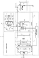
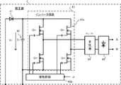
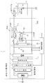
- the DC pulse power supply device of the present invention includes a DC power supply unit (DC unit) 10, a pulse unit 20A for supplying a pulse output generated by a boost chopper circuit connected to the DC power supply unit 10 to a load 4, and a pulse unit 20A.
- the regenerative unit 40 that regenerates the excessive voltage rise that occurs to the DC power supply unit 10 side, the DC power supply unit 10, the pulse unit 20A, and the control circuit unit 50 that controls the regenerative unit 40 are provided, and via the output cable 3.
- the pulse output is supplied to the load 4.
- FIG. 2 shows an example of the plasma generator as the load 4, the load 4 is not limited to the plasma generator, and may be applied to a pulse laser excitation, an electric discharge machine, or the like.
- the regenerative unit 40 included in the DC pulse power supply device 1 of the first configuration example configures the regenerative voltage unit 30A and regenerates the excess voltage increase of the pulse unit 20A to the DC power supply unit 10 side.
- the DC power supply unit (DC unit) 10 includes a rectifier 11 that rectifies the AC voltage of the AC power supply 2 into a DC voltage, and a snubber circuit 12 that absorbs and suppresses spike-like high voltage that occurs transiently during rectification.
- a single-phase inverter circuit 13 for converting a DC voltage into an AC voltage a single-phase transformer 14 for converting the AC voltage of the single-phase inverter circuit 13 into a predetermined voltage value, and a voltage conversion by the single-phase transformer 14.
- a rectifier 11 that rectifies an AC voltage into a DC voltage, and a capacitor 16 (CF) that uses a voltage across the DC voltage of a DC power supply unit are provided.
- FIG. 2 shows an example of the capacitive load of the plasma generator as the load 4.
- one end of the plasma generator is grounded to supply a negative voltage, so that the DC power supply unit 10 is configured to generate a pulse output of a negative voltage.
- the single-phase inverter circuit 13 performs a switching operation according to a control signal from the control circuit unit 50 to convert a DC voltage into an AC voltage having a predetermined frequency.
- Each of the circuit elements of the rectifiers 11 and 15, the snubber circuit 12, the single-phase inverter circuit 13, and the single-phase transformer 14 that configure the DC power supply unit 10 may have any commonly known circuit configuration.
- the pulse unit 20A generates a pulse waveform from the DC voltage by the boost chopper circuit.
- the step-up chopper circuit turns on/off the DC reactor 21A connected in series between the DC power supply side and the load side, the switching element (Q1) 22 connected in parallel to the load side, and the switching element 22.
- the driving circuit 23 for driving is provided.
- the DC reactor 21A is composed of a DC reactor 21a composed of a single-winding transformer without taps.
- the DC power supply side of the pulse unit 20A includes a grounded terminal B and a negative voltage terminal A as a low voltage side.
- the illustrated switching element 22 is an example of an FET, the source S side is connected to the low voltage side, the drain D side is connected to the ground voltage side, and the drive signal from the drive circuit 23 is input to the gate G side.
- control circuit unit 50 In order to operate the step-up chopper circuit, the control circuit unit 50 generates a signal that determines the time width or duty ratio of the ON period and the OFF period of the switching element 22 corresponding to the target pulse output, and the DC power supply unit 10 A control signal is generated based on the voltage and current at the output terminal of the.
- the drive circuit 23 outputs a drive signal to the gate G of the switching element 22 based on the control signal of the control circuit section 50 to cause the switching element 22 to turn on/off.
- the source S side of the switching element 22 is connected to the load side of the DC reactor 21a, and the drain D side of the switching element 22 is grounded.
- the load side of the DC reactor 21a is grounded, and a current flows from the terminal B to the terminal A through the switching element 22 in the ON state and the DC reactor 21a.
- electromagnetic energy is accumulated in the DC reactor 21a.
- a reactor voltage V DCL is generated in the DC reactor 21a due to the stored energy stored in the DC reactor 21a.
- the step-up chopper circuit raises the output voltage Vo according to the duty ratio of the ON/OFF period by repeating the ON operation and the OFF operation of the switching element 22.
- the first configuration example of the DC pulse power supply device of the present invention includes a regenerative voltage unit 30A as the voltage superimposing unit 30.
- FIG. 2 shows a configuration example including the regenerative unit 40 as the regenerative voltage unit 30A.
- the regenerative unit 40 regenerates the DC voltage of the reactor voltage of the DC reactor of the boost chopper circuit that exceeds the set voltage.
- the regeneration unit 40 includes a diode 41, a capacitor 42 (C1), an inverter circuit 43, a transformer 44, and a rectifier 45.
- One end of the capacitor 42 (C1) is connected to the load side end of the DC reactor 21a, the other end is connected to the DC power supply side end of the DC reactor 21a via the diode 41, and the reactor voltage generated in the DC reactor 21a is Is applied.
- the diode 41 is connected such that the direction from the pulse unit 20A to the capacitor 42 (C1) of the regenerative unit 40 is the forward direction, and when the reactor voltage V DCL of the DC reactor 21a exceeds the capacitor voltage V C1 of the capacitor 42 (C1).
- the regeneration unit 40 regenerates the voltage component of which the voltage VDCL exceeds the capacitor voltage VC1 of the capacitor 42 (C1).
- the regenerating unit 40 performs a regenerating operation by using the capacitor voltage VC1 of the capacitor 42 (C1) as a threshold value, and also functions as a constant voltage source that applies the reactor voltage VDCL1 of the DC reactor 21a to the capacitor voltage VC1 during pulse output.
- the output voltage Vo of the pulse output is (VAB+VC1) in which the capacitor voltage VC1 is superimposed on the DC voltage VAB of the DC power supply.
- the capacitor voltage VC1 is a voltage corresponding to the regenerative input voltage Vin in FIG.
- the output voltage Vo of the pulse output is obtained by superimposing (n2/n1) ⁇ VAB on the DC voltage VAB of the DC power source (VAB+(n2/n1) ⁇ VAB).
- the voltage value of (n2/n1) ⁇ VAB of the capacitor voltage VC1 can be changed by changing the transformation ratio (n2:n1) of the transformer 44, and the output voltage Vo of the pulse output is the transformation ratio of the transformer 44. It can be increased by changing (n2:n1).
- the capacitor voltage VC1 can be set not only by changing the transformation ratio of the transformer 44 included in the regenerative unit 40 but also by controlling the output of the inverter circuit 43.
- the output control of the inverter circuit 43 includes, for example, PWM control and phase shift control, but it is not limited to this as long as it is a method of controlling the output of the inverter circuit.
- the regenerative unit 40 has a configuration in which one end is connected to the low-voltage side input end of the pulse unit 20A, and the DC reactor 21a with the low-voltage side voltage (negative voltage) as a reference. Regeneration is performed using the reactor voltage V DCL as the regenerative input voltage Vin.
- the inverter circuit 43 performs orthogonal conversion between the DC voltage on the side of the capacitor 42 and the AC voltage on the side of the transformer 44, and holds the capacitor voltage VC1 of the capacitor 42 (C1) at a constant voltage based on the DC voltage VAB of the DC power supply. At the same time, when the reactor voltage VDCL exceeds the capacitor voltage VC1 of the capacitor 42 (C1), the excess voltage is converted into AC and regenerated to the DC power supply side. Since the capacitor voltage VC1 is held at a constant voltage, the reactor voltage VDDL of the DC reactor 21a is clamped to the capacitor voltage VC1.
- the inverter circuit 43 can be configured by, for example, a bridge circuit of switching elements. The opening/closing operation of the switching element is controlled by the control signal ⁇ from the control circuit unit 50.
- the transformer 44 modulates the voltage ratio between the DC voltage VAB of the DC power supply unit 10 and the capacitor voltage VC1 of the capacitor 42 (C1) based on the transformation ratio.
- the transformation ratio of the transformer 44 is (n2:n1)
- the rectifier 45 rectifies the AC voltage on the transformer 44 side into the DC voltage on the DC power supply unit 10 side.
- the DC side terminal of the rectifier 45 is connected to the terminals A and B of the DC power supply unit 10 and regenerates the regenerated electric power to the DC power supply unit 10 during regeneration, and the capacitor voltage VC1 of the capacitor 42 (C1) while regeneration is not performed. Is held at a voltage based on the DC voltage VAB.
- the configuration of the regenerative unit 40 has a function of clamping the voltage across the DC reactor 21a to a predetermined voltage and outputting a constant voltage, and a function of regenerating the electric power exceeding the predetermined voltage on the DC power supply side.
- the configuration is not limited to the above.
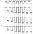
- FIG. 3A shows the ON state (on) and the OFF state (off) of the switching element 22
- FIG. 3B shows the reactor voltage VDDL of the DC reactor 21a
- FIG. The drain-source voltage VDS of the switching element 22 is shown
- FIG. 3D shows the output voltage Vo.
- S1 to S14 in the figure show the ON state and the OFF state of each stage.
- the switching element 22 is in the on state (on) in the states with odd numbers S1, S3,... S13, and the switching element 22 is in the off state with even numbers S2, S4,. (Off) is shown.
- the voltage of the drain-source voltage VDS of the switching element 22 becomes a voltage according to the reactor voltage VDCL and gradually increases, but has not reached the capacitor voltage VC1 of the regenerative unit.
- FIG. 3 shows a state in which the negative voltage value increases (FIG. 3C).
- As the output voltage Vo a voltage component in which the reactor voltage V DCL is superimposed on the DC voltage V AB of the DC power supply is output (FIG. 3(d)).
- the reactor voltage VDCL shown by the solid line shows a state where it is clamped to the capacitor voltage VC1
- the case where the reactor voltage VDCL shown by the broken line is not clamped at the capacitor voltage VC1 is shown as a comparative example.
- the voltage of the drain-source voltage VDS of the switching element 22 becomes a voltage according to the reactor voltage VDCL, and is held at the voltage of the capacitor voltage VC1 of the regenerative unit.
- the drain-source voltage VDS shown by the solid line shows a state of being clamped to the capacitor voltage VC1
- the drain-source voltage VDS shown by the broken line is not being clamped by the capacitor voltage VC1 as a comparative example.
- FIG. 3 shows a state in which the negative voltage value increases (FIG. 3C).
- the output voltage Vo As the output voltage Vo, the voltage component of the DC voltage VAB of the DC power supply and the reactor voltage V DCL is output. Since the reactor voltage VDCL is clamped, the output voltage Vo is held at a constant voltage (FIG. 3(d)).
- FIG. 4A shows the output voltage Vo in the regenerative state in the first configuration example.
- the DC pulse power supply device outputs the pulse output of the output voltage Vo with the switching cycle of the step-up chopper circuit as the pulse cycle T.
- the pulse output has an on period Ton in which the switching element is in the on state and an off period Toff in which the switching element is in the off state within the pulse period T.
- the output voltage Vo during the on period Ton is a voltage value corresponding to the drain-source voltage VDS.
- the output voltage Vo in the off period Toff is the DC voltage VAB of the DC power source with the reactor voltage VDCL superimposed (VAB+VDCL), but the reactor voltage VDCL is clamped to the capacitor voltage VC1 (VAB+VC1). Since the DC voltage VAB and the capacitor voltage VC1 are constant voltages, the output voltage Vo of the pulse output is held at a constant voltage.
- the regenerative unit 40 includes an inverter circuit 43 that outputs an AC voltage obtained by orthogonally converting the DC voltage of the capacitor voltage VC1 of the capacitor 42 (C1) to the transformer 44.
- the inverter circuit 43 includes a bridge circuit 43a including switching elements QR1 to QR4, and a drive circuit 43b that generates a drive signal for driving the switching elements QR1 to QR4 based on the control signal ⁇ . Note that, here, an example of a full bridge circuit is shown as the bridge circuit 43a, but a half bridge circuit or a multi-phase inverter circuit may be used.
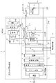
- the second configuration of the DC pulse power supply device of the present invention includes a DC power supply unit (DC unit) 10 and a pulse unit 20B for supplying the load 4 with the pulse output generated by the step-up chopper circuit connected to the DC power supply unit 10.
- the reactor voltage unit 30B provided in the pulse unit 20B, the DC power supply unit 10 and the control circuit unit 50 for controlling the pulse unit 20B are provided, and pulse output is supplied to the load 4 via the output cable 3.
- a second configuration example of the DC pulse power supply device of the present invention will be described with reference to FIG.
- the second configuration example is different from the first configuration example in that the reactor voltage unit 30B is provided in place of the regenerative voltage unit 30A, and the other configurations are the same as the first configuration example.
- a configuration different from the first configuration example will be described, and description of other common configurations will be omitted.
- the DC reactor 21a that constitutes the DC reactor 21A included in the boost chopper circuit of the first configuration example is composed of a single-winding transformer without taps.
- the DC reactor 21B of the second configuration example includes the DC reactor 21a and the second DC reactor 21b that is magnetically coupled, and is used as the tapless single-winding transformer of the step-up chopper circuit of the first configuration example. Instead, it consists of a single-winding transformer with taps.
- the DC reactor 21B by the tapped single-turn transformer has a configuration in which the magnetically coupled DC reactor 21a and the second DC reactor 21b are DC-connected.
- One end of the DC reactor 21a is connected to the terminal A on the low voltage side of the DC power supply, one end of the second DC reactor 21b is connected to the load side, and the connection point between the DC reactor 21a and the second DC reactor 21b is a switching element. 22 is connected to the source S end.
- the tap point of the DC reactor 21B is grounded, and a current flows from the terminal B to the terminal A through the switching element 22 in the ON state and the DC reactor 21a of the DC reactor 21B. At this time, electromagnetic energy is accumulated in the DC reactor 21a.
- the reactor voltage i DCL1 is generated in the DC reactor 21a by the reactor current iL flowing due to the stored energy stored in the DC reactor 21a of the DC reactor 21B, and the second Reactor voltage VDCL2 is generated in DC reactor 21b.
- the boost chopper circuit raises the output voltage Vo by repeating the ON operation and the OFF operation of the switching element 22 as in the first configuration example.
- the voltage ratio between the reactor voltage V DCL1 of the DC reactor 21a and the reactor voltage V DCL2 of the second DC reactor 21b is a value corresponding to the ratio of the inductance ratio of the DC reactor 21a and the second DC reactor 21b.
- the winding number ratio of the single turn coil of the DC reactor 21a of the DC reactor 21B and the second DC reactor 21b is n1p:n2p
- the reactor voltage VDDL1 of the DC reactor 21a and the reactor voltage VDDL2 of the second DC reactor 21b is n1p:n2p
- the reactor voltage VDDL1 of the DC reactor 21a and the reactor voltage VDDL2 of the second DC reactor 21b is the voltage ratio (VDCL1/VDCL2) to the number of turns (n1p/n2p).
- FIG. 4B shows the output voltage Vo in the second configuration example.
- the DC pulse power supply device outputs the pulse output of the output voltage Vo with the switching cycle of the step-up chopper circuit as the pulse cycle T.
- the pulse output has an on period Ton in which the switching element is in the on state and an off period Toff in which the switching element is in the off state within the pulse period T.
- the output voltage Vo during the on period Ton is a voltage value corresponding to the reactor voltage VDCL2.
- the output voltage Vo during the off period Toff is the DC voltage VAB of the DC power supply in which the reactor voltage VDDL1 of the DC reactor 21a and the reactor voltage VDDL2 of the second DC reactor 21b are superimposed (VAB+VDCL1+VDCL2).
- the third configuration of the DC pulse power supply device of the present invention includes a DC power supply unit (DC unit) 10 and a pulse unit 20B that supplies a pulse output generated by a boost chopper circuit connected to the DC power supply unit 10 to the load 4.
- An output cable including a regenerative voltage unit 30A for applying a superimposed voltage component to the DC reactor, a reactor voltage unit 30B provided in the pulse unit 20B, and a control circuit unit 50 for controlling the DC power supply unit 10 and the pulse unit 20B.
- the pulse output is supplied to the load 4 via 3.
- a third configuration example of the DC pulse power supply device of the present invention will be described with reference to FIG.
- the third configuration example is different from the first and second configuration examples in that it includes a regenerative voltage unit 30A and a reactor voltage unit 30B, and other configurations are the same as the first and second configuration examples. is there.
- the regenerative voltage section 30A and the reactor voltage section 30B will be described, and description of other common configurations will be omitted.
- the third configuration example includes a regenerative voltage unit 30A and a reactor voltage unit 30B as a voltage superimposing unit.
- Regenerative voltage unit 30A 30 A of regenerative voltage parts are comprised by the regenerative part like the 1st structural example.
- the configuration example of FIG. 7 shows a configuration example including the regenerative unit 40 as the regenerative voltage unit 30A.
- the regenerative unit 40 regenerates a voltage component exceeding the set voltage among the reactor voltage of the DC reactor of the boost chopper circuit to the DC power supply, and at the time of pulse output, sets the set voltage to the reactor voltage V DCL1 for the DC reactor 21a to the capacitor voltage VC1. It functions as the applied regenerative voltage unit 30A.
- the regeneration unit 40 includes a diode 41, a capacitor 42 (C1), an inverter circuit 43, a transformer 44, and a rectifier 45.
- One end of the capacitor 42 (C1) is connected to the load side end of the DC reactor 21a, the other end is connected to the DC power supply side end of the DC reactor 21a via the diode 41, and the reactor voltage generated in the DC reactor 21a is Is applied.
- the diode 41 is connected such that the direction from the pulse unit 20A to the capacitor 42 (C1) of the regenerative unit 40 is the forward direction, and when the reactor voltage V DCL of the DC reactor 21a exceeds the capacitor voltage V C1 of the capacitor 42 (C1).
- the regeneration unit 40 regenerates the voltage component of which the voltage VDCL exceeds the capacitor voltage VC1 of the capacitor 42 (C1).
- the regenerative unit 40 performs a regenerative operation by using the capacitor voltage VC1 of the capacitor 42 (C1) as a threshold value, and acts as a constant voltage source that applies the reactor voltage V DCL1 of the DC reactor 21a to the capacitor voltage VC 1 at the time of pulse output.
- the output voltage Vo of the pulse output becomes (VAB+VC1+VDCL2) in which the capacitor voltage VC1 and the DC reactor voltage VDCL2 are superimposed on the DC voltage VAB of the DC power supply.
- the capacitor voltage VC1 is a voltage corresponding to the regenerative input voltage Vin in FIG.
- the output voltage Vo of the pulse output is obtained by superimposing (n2/n1) ⁇ AB on the DC voltage VAB of the DC power source (VAB+(n2/n1) ⁇ VAB).
- the voltage (n2/n1) ⁇ VAB can be changed in voltage value by changing the transformation ratio (n2:n1) of the transformer 44, and the output voltage Vo of the pulse output is the transformation ratio (n2: It can be increased by changing n1).
- Reactor voltage unit 30B has the same configuration as the second configuration example, and is configured by a tapped single-winding transformer.
- the reactor voltage unit 30B is configured by a DC reactor 21C including a second DC reactor 21b magnetically coupled to the DC reactor 21a, and the DC reactor 21a and the second DC reactor 21b are configured by a tapped single-winding transformer. ..
- the DC reactor 21C by the tapped single-winding transformer has a configuration in which the magnetically coupled DC reactor 21a and the second DC reactor 21b are DC-connected.
- One end of the DC reactor 21a is connected to the terminal A on the low voltage side of the DC power supply, one end of the second DC reactor 21b is connected to the load side, and the connection point between the DC reactor 21a and the second DC reactor 21b is a switching element. 22 is connected to the source S end.
- the tap point of the DC reactor 21C is grounded, and a current flows from the terminal B to the terminal A through the switching element 22 in the ON state and the DC reactor 21a of the DC reactor 21B. At this time, electromagnetic energy is accumulated in the DC reactor 21a.
- the reactor voltage i DCL1 is generated in the DC reactor 21a by the reactor current iL flowing by the stored energy stored in the DC reactor 21a of the DC reactor 21C, and the second DC reactor 21b. Generates a reactor voltage VDCL2.
- the step-up chopper circuit raises the output voltage Vo by repeating the ON operation and the OFF operation of the switching element 22.
- the voltage ratio between the reactor voltage V DCL1 of the DC reactor 21a and the reactor voltage V DCL2 of the second DC reactor 21b is a value corresponding to the ratio of the inductance ratio of the DC reactor 21a and the second DC reactor 21b.
- the turns ratio of the tapped single-winding transformer of the DC reactor 21a of the DC reactor 21C and the second DC reactor 21b is set to n1p:n2p
- the reactor voltage VDCL1 of the DC reactor 21a and the reactor of the second DC reactor 21b is the winding number ratio (n2p/n1p).
- the reactor voltage V DCL1 of the DC reactor 21a is clamped to the constant voltage of the capacitor voltage VC1 by the regenerative voltage unit 30A, and when the regenerative voltage unit 30A is configured by the regenerative unit, the capacitor voltage VC1 is based on the transformation ratio of the transformer.
- VC1 (n2/n1) ⁇ VAB
- the boost chopper circuit boosts the DC voltage VAB of the DC power supply by turning on/off the switching element with the duty ratio Duty to generate a pulse output with a voltage value of (VAB/(1-Duty)).
- the output voltage Vo has the following two output states depending on the relationship between the pulse output voltage (VAB/(1-Duty)) of the boost chopper circuit and the capacitor voltage VC1 of the capacitor C1 of the regenerative unit.
- the output voltage Vo of the pulse output is the output of the pulse output depending on the transformation ratio (n2/n1) of the transformer in the regenerative unit and the winding number ratio (n2p/n1p) of the DC reactor 21a and the second DC reactor 21b.
- the voltage can be increased.
- FIG. 4C shows the output voltage Vo in the regenerative state in the third configuration example.
- the DC pulse power supply device outputs the pulse output of the output voltage Vo with the switching cycle of the step-up chopper circuit as the pulse cycle T.
- the pulse output has an on period Ton in which the switching element is in the on state and an off period Toff in which the switching element is in the off state within the pulse period T.
- the output voltage Vo during the on period Ton is a voltage value corresponding to the reactor voltage VDCL2.
- the output voltage Vo during the off period Toff is the DC voltage VAB of the DC power supply, the capacitor voltage VC1 and the reactor voltage VDCL2 of the second DC reactor 21b being superimposed (VAB+VC1+VDCL2).
- the fourth configuration of the DC pulse power supply device of the present invention generates a pulse output by the DC power supply unit (DC unit) 10 and the boost chopper circuit connected to the DC power supply unit 10, like the third configuration.
- a pulse unit 20C to be supplied to the load 4 a DC power supply unit 10, a pulse unit 20C, and a control circuit unit 50 for controlling the regenerative unit 40 are provided, and a regenerative voltage unit 30A and a reactor voltage unit 30B are provided as a voltage superimposing unit.
- a pulse output is supplied to the load 4 via the output cable 3.
- a fourth configuration example of the DC pulse power supply device of the present invention will be described with reference to FIG.
- the fourth configuration example is different from the third configuration example in the configuration of the reactor voltage section 30B, and the other configurations are similar to the first and second configuration examples.
- a configuration different from the third configuration example will be described, and description of other common configurations will be omitted.
- the DC reactor 21C that constitutes the reactor voltage unit 30B of the third configuration example is configured by a tapped single-winding transformer.
- the DC reactor 21D that configures the reactor voltage unit 30B of the fourth configuration example is configured by a multi-winding transformer instead of the tapped single-turn transformer of the boost chopper circuit of the third configuration example.
- the DC reactor 21D with a multi-winding transformer has a configuration in which a magnetically coupled DC reactor 21a and a second DC reactor 21b are connected in parallel.
- One end of the DC reactor 21a is connected to the terminal A on the low voltage side of the DC power supply, and the other end is connected to the source S terminal of the switching element 22.
- One end of the second DC reactor 21b is connected to the terminal A on the low voltage side of the DC power supply, and the other end is connected to the load side.
- the reactor voltage iDCL1 is generated in the DC reactor 21a by the reactor current iL flowing by the stored energy stored in the DC reactor 21a of the DC reactor 21D.
- a reactor voltage V DCL2 is generated in the DC reactor 21b by magnetic coupling with the DC reactor 21a.
- the step-up chopper circuit raises the output voltage Vo by repeating the ON operation and the OFF operation of the switching element 22 as in the first and second configuration examples.
- the voltage ratio between the reactor voltage V DCL1 of the DC reactor 21a and the reactor voltage V DCL2 of the second DC reactor 21b is a value corresponding to the ratio of the inductance ratio of the DC reactor 21a and the second DC reactor 21b.
- the winding number ratio of the multi-winding coil of the DC reactor 21a of the DC reactor 21D and the second DC reactor 21b is (n1p:n2p)
- the reactor voltage V DCL1 of the DC reactor 21a and the reactor of the second DC reactor 21b is the winding number ratio (n1p/n2p).
- the DC pulse power supply device of the present invention can be applied as a power source for supplying power to a plasma generator, and can also be used as a power supply device for supplying pulse output to a load such as pulse laser excitation or an electric discharge machine.
Landscapes
- Engineering & Computer Science (AREA)
- Power Engineering (AREA)
- Physics & Mathematics (AREA)
- Plasma & Fusion (AREA)
- Chemical & Material Sciences (AREA)
- Analytical Chemistry (AREA)
- Dc-Dc Converters (AREA)
- Inverter Devices (AREA)
- Amplifiers (AREA)
- Generation Of Surge Voltage And Current (AREA)
Priority Applications (4)
| Application Number | Priority Date | Filing Date | Title |
|---|---|---|---|
| US17/422,469 US11881777B2 (en) | 2019-01-24 | 2019-11-08 | DC pulse power supply device |
| EP19911240.0A EP3916991A4 (en) | 2019-01-24 | 2019-11-08 | DC POWER SUPPLY DEVICE |
| CN201980089853.8A CN113348618A (zh) | 2019-01-24 | 2019-11-08 | 直流脉冲电源装置 |
| KR1020217021135A KR102616569B1 (ko) | 2019-01-24 | 2019-11-08 | 직류 펄스 전원 장치 |
Applications Claiming Priority (2)
| Application Number | Priority Date | Filing Date | Title |
|---|---|---|---|
| JP2019010637A JP7051727B2 (ja) | 2019-01-24 | 2019-01-24 | 直流パルス電源装置 |
| JP2019-010637 | 2019-01-24 |
Publications (1)
| Publication Number | Publication Date |
|---|---|
| WO2020152947A1 true WO2020152947A1 (ja) | 2020-07-30 |
Family
ID=71736189
Family Applications (1)
| Application Number | Title | Priority Date | Filing Date |
|---|---|---|---|
| PCT/JP2019/043836 Ceased WO2020152947A1 (ja) | 2019-01-24 | 2019-11-08 | 直流パルス電源装置 |
Country Status (7)
| Country | Link |
|---|---|
| US (1) | US11881777B2 (enExample) |
| EP (1) | EP3916991A4 (enExample) |
| JP (1) | JP7051727B2 (enExample) |
| KR (1) | KR102616569B1 (enExample) |
| CN (1) | CN113348618A (enExample) |
| TW (1) | TWI816965B (enExample) |
| WO (1) | WO2020152947A1 (enExample) |
Families Citing this family (2)
| Publication number | Priority date | Publication date | Assignee | Title |
|---|---|---|---|---|
| JP7051727B2 (ja) | 2019-01-24 | 2022-04-11 | 株式会社京三製作所 | 直流パルス電源装置 |
| JP6835900B2 (ja) * | 2019-04-11 | 2021-02-24 | 株式会社京三製作所 | 直流パルス電源装置、及び直流パルス電源装置の磁気飽和リセット方法 |
Citations (9)
| Publication number | Priority date | Publication date | Assignee | Title |
|---|---|---|---|---|
| JPS5879470A (ja) * | 1981-10-22 | 1983-05-13 | ウエスタ−ン・エレクトリツク・カムパニ−・インコ−ポレ−テツド | スイツチ式電力調整回路 |
| JPH01252165A (ja) | 1988-03-30 | 1989-10-06 | Toshiba Lighting & Technol Corp | 昇圧チョッパ回路 |
| JPH05327089A (ja) * | 1992-05-26 | 1993-12-10 | Toshiba Corp | パルス充電回路 |
| JPH08222258A (ja) | 1995-02-15 | 1996-08-30 | Fuji Electric Co Ltd | 燃料電池発電装置 |
| JP2004080880A (ja) * | 2002-08-13 | 2004-03-11 | Fuji Electric Holdings Co Ltd | スナバ回路 |
| JP2006006053A (ja) | 2004-06-18 | 2006-01-05 | Shihen Tech Corp | 直流電源装置 |
| US7023186B2 (en) * | 2004-08-05 | 2006-04-04 | Astec International Limited | Two stage boost converter topology |
| JP2012178952A (ja) | 2011-02-28 | 2012-09-13 | Sanken Electric Co Ltd | スイッチング電源回路 |
| JP2012196080A (ja) * | 2011-03-17 | 2012-10-11 | Nippon Soken Inc | スイッチング電源装置 |
Family Cites Families (17)
| Publication number | Priority date | Publication date | Assignee | Title |
|---|---|---|---|---|
| JPH02219461A (ja) * | 1989-02-16 | 1990-09-03 | Nippon Telegr & Teleph Corp <Ntt> | 巻上げコイル付昇圧形dc―dcコンバータ |
| JP2630221B2 (ja) * | 1993-10-08 | 1997-07-16 | 日本電気株式会社 | Dc−dcコンバータ |
| US5929614A (en) * | 1997-06-13 | 1999-07-27 | Northrop Grumman Corporation | High efficiency DC step-up voltage converter |
| US6043636A (en) | 1997-10-20 | 2000-03-28 | Diversified Technologies, Inc. | Voltage transient suppression |
| US5982646A (en) | 1998-06-30 | 1999-11-09 | General Electric Company | Voltage clamp snubbers for three level converter |
| US6380722B2 (en) * | 2000-02-28 | 2002-04-30 | Intel Corporation | Method to increase the efficiency of a power switching device |
| JP2002218743A (ja) * | 2001-01-23 | 2002-08-02 | Meidensha Corp | コンデンサの充電装置 |
| US6822427B2 (en) | 2002-05-01 | 2004-11-23 | Technical Witts, Inc. | Circuits and circuit elements for high efficiency power conversion |
| ITTO20030550A1 (it) * | 2003-07-15 | 2005-01-16 | Fiat Ricerche | Circuito elevatore di tensione per l'alimentazione di |
| US20070053217A1 (en) | 2005-09-02 | 2007-03-08 | Lear Corporation | Converter for automotive use |
| JP5794006B2 (ja) | 2011-07-15 | 2015-10-14 | 株式会社明電舎 | コンデンサの充電器 |
| US20150085534A1 (en) | 2013-09-20 | 2015-03-26 | Alexander ABRAMOVITZ | Regenerative and ramping acceleration (rara) snubbers for isolated and tapped-inductor converters |
| GB2523386B (en) * | 2014-02-24 | 2016-07-06 | Tdk-Lambda Uk Ltd | Snubber |
| CN105515392B (zh) * | 2015-12-28 | 2018-06-01 | 深圳茂硕电气有限公司 | 一种直流-直流升压变换电路 |
| US9780676B2 (en) | 2016-02-22 | 2017-10-03 | Infineon Technologies Austria Ag | Power converter with a snubber circuit |
| CN106452083B (zh) * | 2016-10-17 | 2018-09-21 | 盐城工学院 | 高增益直流电压提升变换电路 |
| JP7051727B2 (ja) | 2019-01-24 | 2022-04-11 | 株式会社京三製作所 | 直流パルス電源装置 |
-
2019
- 2019-01-24 JP JP2019010637A patent/JP7051727B2/ja active Active
- 2019-11-08 CN CN201980089853.8A patent/CN113348618A/zh active Pending
- 2019-11-08 KR KR1020217021135A patent/KR102616569B1/ko active Active
- 2019-11-08 EP EP19911240.0A patent/EP3916991A4/en not_active Withdrawn
- 2019-11-08 US US17/422,469 patent/US11881777B2/en active Active
- 2019-11-08 WO PCT/JP2019/043836 patent/WO2020152947A1/ja not_active Ceased
-
2020
- 2020-01-06 TW TW109100284A patent/TWI816965B/zh active
Patent Citations (9)
| Publication number | Priority date | Publication date | Assignee | Title |
|---|---|---|---|---|
| JPS5879470A (ja) * | 1981-10-22 | 1983-05-13 | ウエスタ−ン・エレクトリツク・カムパニ−・インコ−ポレ−テツド | スイツチ式電力調整回路 |
| JPH01252165A (ja) | 1988-03-30 | 1989-10-06 | Toshiba Lighting & Technol Corp | 昇圧チョッパ回路 |
| JPH05327089A (ja) * | 1992-05-26 | 1993-12-10 | Toshiba Corp | パルス充電回路 |
| JPH08222258A (ja) | 1995-02-15 | 1996-08-30 | Fuji Electric Co Ltd | 燃料電池発電装置 |
| JP2004080880A (ja) * | 2002-08-13 | 2004-03-11 | Fuji Electric Holdings Co Ltd | スナバ回路 |
| JP2006006053A (ja) | 2004-06-18 | 2006-01-05 | Shihen Tech Corp | 直流電源装置 |
| US7023186B2 (en) * | 2004-08-05 | 2006-04-04 | Astec International Limited | Two stage boost converter topology |
| JP2012178952A (ja) | 2011-02-28 | 2012-09-13 | Sanken Electric Co Ltd | スイッチング電源回路 |
| JP2012196080A (ja) * | 2011-03-17 | 2012-10-11 | Nippon Soken Inc | スイッチング電源装置 |
Non-Patent Citations (1)
| Title |
|---|
| See also references of EP3916991A4 |
Also Published As
| Publication number | Publication date |
|---|---|
| EP3916991A4 (en) | 2022-09-28 |
| US11881777B2 (en) | 2024-01-23 |
| US20220094266A1 (en) | 2022-03-24 |
| TW202046623A (zh) | 2020-12-16 |
| KR102616569B1 (ko) | 2023-12-27 |
| KR20210100157A (ko) | 2021-08-13 |
| CN113348618A (zh) | 2021-09-03 |
| EP3916991A1 (en) | 2021-12-01 |
| TWI816965B (zh) | 2023-10-01 |
| JP7051727B2 (ja) | 2022-04-11 |
| JP2020120522A (ja) | 2020-08-06 |
Similar Documents
| Publication | Publication Date | Title |
|---|---|---|
| US6717827B2 (en) | Switching power supply | |
| US8441812B2 (en) | Series resonant converter having a circuit configuration that prevents leading current | |
| JP5585408B2 (ja) | スイッチング電源装置 | |
| JP7329971B2 (ja) | コンバータ | |
| JP2010124567A (ja) | スイッチング電源装置 | |
| WO2020152947A1 (ja) | 直流パルス電源装置 | |
| TWI816966B (zh) | 直流脈衝電源裝置 | |
| JP7051726B2 (ja) | 直流パルス電源装置 | |
| CN115664223B (zh) | 一种准z源全桥变换器和控制方法 | |
| KR20210124480A (ko) | 직류 펄스 전원 장치, 및 직류 펄스 전원 장치의 듀티 제어 방법 | |
| JP4764980B2 (ja) | 直流−直流変換装置 | |
| TWI752360B (zh) | 具寬電壓範圍之雙向隔離式多階直流-直流電能轉換裝置及其方法 | |
| KR20110002223A (ko) | 직렬공진형 컨버터 | |
| KR101182292B1 (ko) | 전압 컨버터 | |
| JP2007159178A (ja) | スイッチング電源装置 | |
| JP2006203996A (ja) | Dc/dcコンバータ |
Legal Events
| Date | Code | Title | Description |
|---|---|---|---|
| 121 | Ep: the epo has been informed by wipo that ep was designated in this application |
Ref document number: 19911240 Country of ref document: EP Kind code of ref document: A1 |
|
| ENP | Entry into the national phase |
Ref document number: 20217021135 Country of ref document: KR Kind code of ref document: A |
|
| NENP | Non-entry into the national phase |
Ref country code: DE |
|
| ENP | Entry into the national phase |
Ref document number: 2019911240 Country of ref document: EP Effective date: 20210824 |