WO2020149401A1 - 金属材および接続端子 - Google Patents
金属材および接続端子 Download PDFInfo
- Publication number
- WO2020149401A1 WO2020149401A1 PCT/JP2020/001479 JP2020001479W WO2020149401A1 WO 2020149401 A1 WO2020149401 A1 WO 2020149401A1 JP 2020001479 W JP2020001479 W JP 2020001479W WO 2020149401 A1 WO2020149401 A1 WO 2020149401A1
- Authority
- WO
- WIPO (PCT)
- Prior art keywords
- surface layer
- layer
- metal material
- metal
- concentration
- Prior art date
- Legal status (The legal status is an assumption and is not a legal conclusion. Google has not performed a legal analysis and makes no representation as to the accuracy of the status listed.)
- Ceased
Links
Images



Classifications
-
- C—CHEMISTRY; METALLURGY
- C23—COATING METALLIC MATERIAL; COATING MATERIAL WITH METALLIC MATERIAL; CHEMICAL SURFACE TREATMENT; DIFFUSION TREATMENT OF METALLIC MATERIAL; COATING BY VACUUM EVAPORATION, BY SPUTTERING, BY ION IMPLANTATION OR BY CHEMICAL VAPOUR DEPOSITION, IN GENERAL; INHIBITING CORROSION OF METALLIC MATERIAL OR INCRUSTATION IN GENERAL
- C23C—COATING METALLIC MATERIAL; COATING MATERIAL WITH METALLIC MATERIAL; SURFACE TREATMENT OF METALLIC MATERIAL BY DIFFUSION INTO THE SURFACE, BY CHEMICAL CONVERSION OR SUBSTITUTION; COATING BY VACUUM EVAPORATION, BY SPUTTERING, BY ION IMPLANTATION OR BY CHEMICAL VAPOUR DEPOSITION, IN GENERAL
- C23C28/00—Coating for obtaining at least two superposed coatings either by methods not provided for in a single one of groups C23C2/00 - C23C26/00 or by combinations of methods provided for in subclasses C23C and C25C or C25D
- C23C28/02—Coating for obtaining at least two superposed coatings either by methods not provided for in a single one of groups C23C2/00 - C23C26/00 or by combinations of methods provided for in subclasses C23C and C25C or C25D only coatings only including layers of metallic material
-
- H—ELECTRICITY
- H01—ELECTRIC ELEMENTS
- H01R—ELECTRICALLY-CONDUCTIVE CONNECTIONS; STRUCTURAL ASSOCIATIONS OF A PLURALITY OF MUTUALLY-INSULATED ELECTRICAL CONNECTING ELEMENTS; COUPLING DEVICES; CURRENT COLLECTORS
- H01R13/00—Details of coupling devices of the kinds covered by groups H01R12/70 or H01R24/00 - H01R33/00
- H01R13/02—Contact members
- H01R13/03—Contact members characterised by the material, e.g. plating, or coating materials
-
- B—PERFORMING OPERATIONS; TRANSPORTING
- B32—LAYERED PRODUCTS
- B32B—LAYERED PRODUCTS, i.e. PRODUCTS BUILT-UP OF STRATA OF FLAT OR NON-FLAT, e.g. CELLULAR OR HONEYCOMB, FORM
- B32B15/00—Layered products comprising a layer of metal
- B32B15/01—Layered products comprising a layer of metal all layers being exclusively metallic
-
- B—PERFORMING OPERATIONS; TRANSPORTING
- B32—LAYERED PRODUCTS
- B32B—LAYERED PRODUCTS, i.e. PRODUCTS BUILT-UP OF STRATA OF FLAT OR NON-FLAT, e.g. CELLULAR OR HONEYCOMB, FORM
- B32B15/00—Layered products comprising a layer of metal
- B32B15/01—Layered products comprising a layer of metal all layers being exclusively metallic
- B32B15/018—Layered products comprising a layer of metal all layers being exclusively metallic one layer being formed of a noble metal or a noble metal alloy
-
- C—CHEMISTRY; METALLURGY
- C23—COATING METALLIC MATERIAL; COATING MATERIAL WITH METALLIC MATERIAL; CHEMICAL SURFACE TREATMENT; DIFFUSION TREATMENT OF METALLIC MATERIAL; COATING BY VACUUM EVAPORATION, BY SPUTTERING, BY ION IMPLANTATION OR BY CHEMICAL VAPOUR DEPOSITION, IN GENERAL; INHIBITING CORROSION OF METALLIC MATERIAL OR INCRUSTATION IN GENERAL
- C23C—COATING METALLIC MATERIAL; COATING MATERIAL WITH METALLIC MATERIAL; SURFACE TREATMENT OF METALLIC MATERIAL BY DIFFUSION INTO THE SURFACE, BY CHEMICAL CONVERSION OR SUBSTITUTION; COATING BY VACUUM EVAPORATION, BY SPUTTERING, BY ION IMPLANTATION OR BY CHEMICAL VAPOUR DEPOSITION, IN GENERAL
- C23C18/00—Chemical coating by decomposition of either liquid compounds or solutions of the coating forming compounds, without leaving reaction products of surface material in the coating; Contact plating
- C23C18/16—Chemical coating by decomposition of either liquid compounds or solutions of the coating forming compounds, without leaving reaction products of surface material in the coating; Contact plating by reduction or substitution, e.g. electroless plating
- C23C18/1601—Process or apparatus
- C23C18/1633—Process of electroless plating
- C23C18/1646—Characteristics of the product obtained
- C23C18/165—Multilayered product
- C23C18/1651—Two or more layers only obtained by electroless plating
-
- C—CHEMISTRY; METALLURGY
- C23—COATING METALLIC MATERIAL; COATING MATERIAL WITH METALLIC MATERIAL; CHEMICAL SURFACE TREATMENT; DIFFUSION TREATMENT OF METALLIC MATERIAL; COATING BY VACUUM EVAPORATION, BY SPUTTERING, BY ION IMPLANTATION OR BY CHEMICAL VAPOUR DEPOSITION, IN GENERAL; INHIBITING CORROSION OF METALLIC MATERIAL OR INCRUSTATION IN GENERAL
- C23C—COATING METALLIC MATERIAL; COATING MATERIAL WITH METALLIC MATERIAL; SURFACE TREATMENT OF METALLIC MATERIAL BY DIFFUSION INTO THE SURFACE, BY CHEMICAL CONVERSION OR SUBSTITUTION; COATING BY VACUUM EVAPORATION, BY SPUTTERING, BY ION IMPLANTATION OR BY CHEMICAL VAPOUR DEPOSITION, IN GENERAL
- C23C28/00—Coating for obtaining at least two superposed coatings either by methods not provided for in a single one of groups C23C2/00 - C23C26/00 or by combinations of methods provided for in subclasses C23C and C25C or C25D
- C23C28/02—Coating for obtaining at least two superposed coatings either by methods not provided for in a single one of groups C23C2/00 - C23C26/00 or by combinations of methods provided for in subclasses C23C and C25C or C25D only coatings only including layers of metallic material
- C23C28/021—Coating for obtaining at least two superposed coatings either by methods not provided for in a single one of groups C23C2/00 - C23C26/00 or by combinations of methods provided for in subclasses C23C and C25C or C25D only coatings only including layers of metallic material including at least one metal alloy layer
-
- C—CHEMISTRY; METALLURGY
- C23—COATING METALLIC MATERIAL; COATING MATERIAL WITH METALLIC MATERIAL; CHEMICAL SURFACE TREATMENT; DIFFUSION TREATMENT OF METALLIC MATERIAL; COATING BY VACUUM EVAPORATION, BY SPUTTERING, BY ION IMPLANTATION OR BY CHEMICAL VAPOUR DEPOSITION, IN GENERAL; INHIBITING CORROSION OF METALLIC MATERIAL OR INCRUSTATION IN GENERAL
- C23C—COATING METALLIC MATERIAL; COATING MATERIAL WITH METALLIC MATERIAL; SURFACE TREATMENT OF METALLIC MATERIAL BY DIFFUSION INTO THE SURFACE, BY CHEMICAL CONVERSION OR SUBSTITUTION; COATING BY VACUUM EVAPORATION, BY SPUTTERING, BY ION IMPLANTATION OR BY CHEMICAL VAPOUR DEPOSITION, IN GENERAL
- C23C28/00—Coating for obtaining at least two superposed coatings either by methods not provided for in a single one of groups C23C2/00 - C23C26/00 or by combinations of methods provided for in subclasses C23C and C25C or C25D
- C23C28/02—Coating for obtaining at least two superposed coatings either by methods not provided for in a single one of groups C23C2/00 - C23C26/00 or by combinations of methods provided for in subclasses C23C and C25C or C25D only coatings only including layers of metallic material
- C23C28/023—Coating for obtaining at least two superposed coatings either by methods not provided for in a single one of groups C23C2/00 - C23C26/00 or by combinations of methods provided for in subclasses C23C and C25C or C25D only coatings only including layers of metallic material only coatings of metal elements only
-
- C—CHEMISTRY; METALLURGY
- C23—COATING METALLIC MATERIAL; COATING MATERIAL WITH METALLIC MATERIAL; CHEMICAL SURFACE TREATMENT; DIFFUSION TREATMENT OF METALLIC MATERIAL; COATING BY VACUUM EVAPORATION, BY SPUTTERING, BY ION IMPLANTATION OR BY CHEMICAL VAPOUR DEPOSITION, IN GENERAL; INHIBITING CORROSION OF METALLIC MATERIAL OR INCRUSTATION IN GENERAL
- C23C—COATING METALLIC MATERIAL; COATING MATERIAL WITH METALLIC MATERIAL; SURFACE TREATMENT OF METALLIC MATERIAL BY DIFFUSION INTO THE SURFACE, BY CHEMICAL CONVERSION OR SUBSTITUTION; COATING BY VACUUM EVAPORATION, BY SPUTTERING, BY ION IMPLANTATION OR BY CHEMICAL VAPOUR DEPOSITION, IN GENERAL
- C23C28/00—Coating for obtaining at least two superposed coatings either by methods not provided for in a single one of groups C23C2/00 - C23C26/00 or by combinations of methods provided for in subclasses C23C and C25C or C25D
- C23C28/30—Coatings combining at least one metallic layer and at least one inorganic non-metallic layer
- C23C28/32—Coatings combining at least one metallic layer and at least one inorganic non-metallic layer including at least one pure metallic layer
- C23C28/321—Coatings combining at least one metallic layer and at least one inorganic non-metallic layer including at least one pure metallic layer with at least one metal alloy layer
-
- C—CHEMISTRY; METALLURGY
- C23—COATING METALLIC MATERIAL; COATING MATERIAL WITH METALLIC MATERIAL; CHEMICAL SURFACE TREATMENT; DIFFUSION TREATMENT OF METALLIC MATERIAL; COATING BY VACUUM EVAPORATION, BY SPUTTERING, BY ION IMPLANTATION OR BY CHEMICAL VAPOUR DEPOSITION, IN GENERAL; INHIBITING CORROSION OF METALLIC MATERIAL OR INCRUSTATION IN GENERAL
- C23C—COATING METALLIC MATERIAL; COATING MATERIAL WITH METALLIC MATERIAL; SURFACE TREATMENT OF METALLIC MATERIAL BY DIFFUSION INTO THE SURFACE, BY CHEMICAL CONVERSION OR SUBSTITUTION; COATING BY VACUUM EVAPORATION, BY SPUTTERING, BY ION IMPLANTATION OR BY CHEMICAL VAPOUR DEPOSITION, IN GENERAL
- C23C28/00—Coating for obtaining at least two superposed coatings either by methods not provided for in a single one of groups C23C2/00 - C23C26/00 or by combinations of methods provided for in subclasses C23C and C25C or C25D
- C23C28/30—Coatings combining at least one metallic layer and at least one inorganic non-metallic layer
- C23C28/32—Coatings combining at least one metallic layer and at least one inorganic non-metallic layer including at least one pure metallic layer
- C23C28/322—Coatings combining at least one metallic layer and at least one inorganic non-metallic layer including at least one pure metallic layer only coatings of metal elements only
-
- C—CHEMISTRY; METALLURGY
- C23—COATING METALLIC MATERIAL; COATING MATERIAL WITH METALLIC MATERIAL; CHEMICAL SURFACE TREATMENT; DIFFUSION TREATMENT OF METALLIC MATERIAL; COATING BY VACUUM EVAPORATION, BY SPUTTERING, BY ION IMPLANTATION OR BY CHEMICAL VAPOUR DEPOSITION, IN GENERAL; INHIBITING CORROSION OF METALLIC MATERIAL OR INCRUSTATION IN GENERAL
- C23C—COATING METALLIC MATERIAL; COATING MATERIAL WITH METALLIC MATERIAL; SURFACE TREATMENT OF METALLIC MATERIAL BY DIFFUSION INTO THE SURFACE, BY CHEMICAL CONVERSION OR SUBSTITUTION; COATING BY VACUUM EVAPORATION, BY SPUTTERING, BY ION IMPLANTATION OR BY CHEMICAL VAPOUR DEPOSITION, IN GENERAL
- C23C28/00—Coating for obtaining at least two superposed coatings either by methods not provided for in a single one of groups C23C2/00 - C23C26/00 or by combinations of methods provided for in subclasses C23C and C25C or C25D
- C23C28/30—Coatings combining at least one metallic layer and at least one inorganic non-metallic layer
- C23C28/34—Coatings combining at least one metallic layer and at least one inorganic non-metallic layer including at least one inorganic non-metallic material layer, e.g. metal carbide, nitride, boride, silicide layer and their mixtures, enamels, phosphates and sulphates
- C23C28/345—Coatings combining at least one metallic layer and at least one inorganic non-metallic layer including at least one inorganic non-metallic material layer, e.g. metal carbide, nitride, boride, silicide layer and their mixtures, enamels, phosphates and sulphates with at least one oxide layer
-
- C—CHEMISTRY; METALLURGY
- C23—COATING METALLIC MATERIAL; COATING MATERIAL WITH METALLIC MATERIAL; CHEMICAL SURFACE TREATMENT; DIFFUSION TREATMENT OF METALLIC MATERIAL; COATING BY VACUUM EVAPORATION, BY SPUTTERING, BY ION IMPLANTATION OR BY CHEMICAL VAPOUR DEPOSITION, IN GENERAL; INHIBITING CORROSION OF METALLIC MATERIAL OR INCRUSTATION IN GENERAL
- C23C—COATING METALLIC MATERIAL; COATING MATERIAL WITH METALLIC MATERIAL; SURFACE TREATMENT OF METALLIC MATERIAL BY DIFFUSION INTO THE SURFACE, BY CHEMICAL CONVERSION OR SUBSTITUTION; COATING BY VACUUM EVAPORATION, BY SPUTTERING, BY ION IMPLANTATION OR BY CHEMICAL VAPOUR DEPOSITION, IN GENERAL
- C23C30/00—Coating with metallic material characterised only by the composition of the metallic material, i.e. not characterised by the coating process
-
- H—ELECTRICITY
- H01—ELECTRIC ELEMENTS
- H01R—ELECTRICALLY-CONDUCTIVE CONNECTIONS; STRUCTURAL ASSOCIATIONS OF A PLURALITY OF MUTUALLY-INSULATED ELECTRICAL CONNECTING ELEMENTS; COUPLING DEVICES; CURRENT COLLECTORS
- H01R13/00—Details of coupling devices of the kinds covered by groups H01R12/70 or H01R24/00 - H01R33/00
- H01R13/02—Contact members
- H01R13/10—Sockets for co-operation with pins or blades
- H01R13/11—Resilient sockets
- H01R13/111—Resilient sockets co-operating with pins having a circular transverse section
Definitions
- the present disclosure relates to metal materials and connection terminals.
- Au layer may be provided on the surface of an electrical connection member such as a connection terminal.
- Gold (Au) has high electrical conductivity and high melting point, and is also resistant to oxidation. Therefore, when a high temperature environment is assumed, the electrical connecting member having the Au layer on its surface can be preferably used. For example, in an automobile, if a connection terminal having an Au layer on its surface is used as a connection terminal used in a high temperature environment such as around an engine, the surface of the Au layer maintains a low contact resistance even at high temperatures. In addition, stable electrical connection characteristics can be obtained.
- Au is a relatively soft metal, and when it is provided on the surface of an electrical connection member such as a connection terminal, lack of hardness tends to be a problem such as an increase in friction coefficient during sliding. Therefore, hard gold having a hardness higher than that of pure Au may be used.
- a plating solution to which an additive element such as Co is added is used. By containing a small amount of Co in the Au layer formed by plating, the hardness of the Au layer is increased.
- the Au is a metal which is not easily oxidized, it is easy to keep the surface of the surface of the electrical connection member such as the connection terminal with a low contact resistance by providing the Au layer on the surface.
- additional elements such as Co contained in the hard gold diffuse to the surface, May undergo oxidation. Then, the contact resistance of the surface may increase due to the contribution of the oxide of the additional element.
- metals such as Ni that are more easily oxidized than Au are often present below the Au layer as a base material or an intermediate layer. Even when these metals diffuse to the surface of the Au layer during heating and undergo oxidation, the contact resistance of the surface may increase due to the contribution of the oxides of these metals.
- the metal material of the present disclosure has a base material and a surface layer formed on the base material, and the surface layer contains Au and In, and at least In is present on the outermost surface. ..
- connection terminal of the present disclosure is made of the metal material as described above, and the surface layer is formed on the surface of the base material at least at a contact portion that makes electrical contact with the counterpart conductive member.
- the metal material and the connection terminal of the present disclosure have a surface layer containing Au, and can maintain a low contact resistance state even when heated.
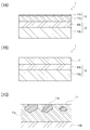
- FIG. 1A to 1C are cross-sectional views schematically showing a laminated structure of a metal material according to an embodiment of the present disclosure.
- FIG. 1A shows the configuration of the entire cross section in the case where the surface layer has a multi-layer structure and
- FIG. 1B shows the example when the surface layer has a single-layer structure.
- FIG. 1C is an enlarged view showing an example of the state of the surface layer having a single layer structure.
- FIG. 2 is a cross-sectional view illustrating the outline of the connection terminal according to the embodiment of the present disclosure.
- 3A to 3C are diagrams showing element concentration distributions of each sample after heating, which are obtained by depth analysis Auger electron spectroscopy. 3A shows the sample A1, FIG. 3B shows the sample A2, and FIG. 3C shows the sample B1.
- FIG. 4 is a diagram showing a result of X-ray diffraction for the sample A1.
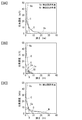
- 5A to 5C are diagrams showing the contact resistance of each sample in the initial state and the state after heating.
- 5A shows sample A1
- FIG. 5B shows sample A2
- FIG. 5C shows sample B1.
- the metal material of the present disclosure has a base material and a surface layer formed on the base material, and the surface layer contains Au and In, and at least In is present on the outermost surface. ..
- the metal material according to the present disclosure contains In in addition to Au in the surface layer.
- In it is possible to suppress the diffusion of the metal (other metal) other than Au and In existing in or under the surface layer to the outermost surface when the temperature of the metal material becomes high. You can As a result, an increase in contact resistance due to the oxidation of another metal on the outermost surface is less likely to occur, and the low contact resistance obtained by Au's high electrical conductivity and oxidation resistance can be maintained before and after heating. it can. Even if In is oxidized on the outermost surface, the oxide film is easily destroyed by application of a load or the like, and thus it is difficult to contribute to increase in contact resistance.
- At least one of the surface layer and the base material contains an easily oxidizable metal other than In that is more susceptible to oxidation than Au, and when the metal material is heated at 170° C.
- the increase in the concentration of the easily oxidizable metal is preferably below the detection limit by Auger electron spectroscopy. In this case, it means that due to the effect of containing In in the surface layer, diffusion of the oxidizable metal to the outermost surface can be sufficiently suppressed when the metal material is heated. Therefore, the increase in contact resistance due to the oxidation of the oxidizable metal on the outermost surface can be effectively suppressed.
- At least a part of In in the surface layer preferably constitutes an Au—In alloy.
- the surface layer containing In in addition to Au can be stably formed and easily maintained.
- the Au—In alloy has an effect of suppressing diffusion of other metal existing in the layer of the surface layer or under the surface layer to the outermost surface due to the contribution of In.
- the oxide film formed on the surface has a property of being easily broken. Therefore, the Au—In alloy exhibits an excellent effect in suppressing an increase in contact resistance during heating in the surface layer.
- the Au—In alloy is preferably a solid solution in which In is solid-dissolved in Au. Then, since In has a characteristic of being easily solid-dissolved in Au, a surface layer containing In in addition to Au can be stably formed, and environmental stability becomes high.
- both Au and In should be present on the outermost surface. Then, both the high electrical conductivity and the hard-to-oxidize property of Au and the effect of suppressing the diffusion of other metals by In are effectively utilized on the outermost surface to form a surface layer having a low contact resistance before and after heating. You can
- the surface layer may include an Au portion containing Au as a main component and a high-concentration In portion containing a higher concentration of In than the Au portion. Then, the high-concentration In portion having a high In concentration is formed, so that the high-concentration In portion can effectively achieve the diffusion suppression of the other metal.
- the high concentration In portion is preferably formed on the surface of the Au portion and exposed on the outermost surface. Then, since the high-concentration In portion constitutes the outermost surface of the surface layer, it is possible to effectively suppress an increase in contact resistance due to the diffusion and oxidation of other metal on the outermost surface during heating. it can.
- the entire surface layer may have a single-layer structure configured as a single layer containing an Au—In alloy.
- the inclusion of In can suppress the diffusion and oxidation of other metal to the outermost surface due to heating.
- the surface layer having a single-layer structure is composed of a homogeneous Au—In alloy as a whole, there are two types of phases, an Au portion having a relatively high Au concentration and a high concentration In portion having a relatively high In concentration. May have.
- the Au layer and the In layer are laminated in this order to form the surface layer, if the In content relative to Au is increased, a single layer structure is likely to be formed.
- In is preferably distributed in the surface layer at a depth of at least 0.01 ⁇ m from the outermost surface. Further, in the surface layer, In may be distributed in a region from the outermost surface to a depth of at least 0.05 ⁇ m. Then, due to In, it becomes easy to sufficiently suppress the diffusion of other metal and the increase in contact resistance during heating.
- the base material has an intermediate layer formed on a base material, and the intermediate layer preferably contains at least one of Ni, Cr, Mn, Fe, Co, and Cu. Then, those metals are metals that are easily oxidized, but since the surface layer contains In, it diffuses into the surface layer during heating and is oxidized, and it becomes difficult to contribute to increase the contact resistance. ..
- the above surface layer preferably contains Co. Then, the hardness of the surface layer can be increased by the effect of containing Co.
- Co is a metal that easily diffuses into the surface of the layer containing Au and is oxidized during heating to increase the contact resistance, but the inclusion of In in the surface layer suppresses the diffusion of Co and reduces the contact. A low resistance state is easily maintained.
- the content of additive elements other than Au and In in the surface layer is preferably 5% or less. Then, the characteristics imparted to the surface layer by Au and In are not easily impaired by the addition of the additional element.
- the content of In in the surface layer as a whole is preferably 10% or more in terms of atomic ratio with respect to Au. Then, the characteristics imparted to the surface layer by In, such as suppressing diffusion of other metals, are effectively exhibited.
- the content of In in the surface layer as a whole is preferably smaller than Au in terms of the number of atoms. Then, the characteristics imparted to the surface layer by Au, such as reduction of the contact resistance on the surface, are effectively exhibited.
- the thickness of the surface layer is preferably 0.1 ⁇ m or more. Then, the characteristics of the surface layer provided by Au and In can be sufficiently exhibited.
- connection terminal according to the present disclosure is made of the metal material, and the surface layer is formed on the surface of the base material at least at a contact portion that makes electrical contact with the counterpart conductive member.
- the surface layer as described above is formed at least in the contact portion, so that the contact portion can maintain low contact resistance even after being heated.
- the content (concentration) of each element is indicated by the atomic number ratio such as atomic% as a unit.
- the case where an unavoidable impurity is contained in the elemental metal is also included.
- the alloy includes both a solid solution and an intermetallic compound.
- a certain metal element as a main component means a state in which the element occupies 50 atomic% or more of all metal species.
- a metal material according to an embodiment of the present disclosure is configured by stacking metal materials.
- the metal material according to the embodiment of the present disclosure may be any metal member, but can be preferably used as a material for forming an electrical connection member such as a connection terminal.
- composition of metal material 1A and 1B show an example of a laminated structure of a metal material 1 according to an embodiment of the present disclosure.
- the metal material 1 has a base material 10 and a surface layer 11 formed on the surface of the base material 10 and exposed on the outermost surface.
- the surface layer 11 contains gold (Au) and indium (In), and may have a multi-layer structure as shown in FIG. 1A or a single-layer structure as shown in FIG. 1B.
- a thin film (not shown) such as an organic layer may be provided on the surface layer 11 exposed on the outermost surface of the metal material 1 as long as the characteristics of the surface layer 11 are not impaired.
- the base material 10 may be made of a single metal material, but preferably includes a base material 10a and an intermediate layer 10b.
- the intermediate layer 10b is formed on the surface of the base material 10a as a metal layer thinner than the base material 10a.
- the base material 10a can be made of a metal material having an arbitrary shape such as a plate shape.
- the material forming the base material 10a is not particularly limited, but when the metal material 1 forms an electric connection member such as a connection terminal, Cu is used as the material forming the base material 10a.
- Cu alloy, Al or Al alloy, Fe or Fe alloy, or the like can be preferably used. Among them, Cu or Cu alloy having excellent electric conductivity can be preferably used.
- the material forming the intermediate layer 10b include metal materials containing at least one selected from the group (A group) of Ni, Cr, Mn, Fe, Co, and Cu.
- the material forming the intermediate layer 10b may be a single metal composed of one kind selected from the group A, or an alloy containing one kind or two or more kinds of metal elements selected from the group A. ..
- the intermediate layer 10b may be composed of only one layer or may be a laminate of two or more layers. Even when the base material 10 does not have the intermediate layer 10b and is made of a single metal material, at least the surface of the single metal material contains at least one selected from the group A. It is preferably composed of
- the intermediate layer 10b contains as a main component a metal containing at least one selected from the group A, particularly a metal element selected from the group A.
- the Cu composition diffuses from the base material 10a to the surface layer 11, and further influences the composition and characteristics of the surface layer 11 such as consumption of In due to alloying with the diffused Cu. It is possible to effectively suppress the occurrence of the phenomenon even under high temperature conditions.
- the intermediate layer 10b is made of Ni or an alloy containing Ni as a main component, it is possible to effectively achieve the suppression of Cu diffusion into the surface layer 11.
- the thickness of the intermediate layer 10b is not particularly limited, it is preferably 0.1 ⁇ m or more from the viewpoint of effectively achieving diffusion suppression between the base material 10a and the surface layer 11. On the other hand, from the viewpoint of avoiding forming the excessively thick intermediate layer 10b, its thickness is preferably 3 ⁇ m or less.
- a part of the base material 10a side may form an alloy with the constituent element of the base material 10a, and a part of the surface layer 11 side forms an alloy with the constituent element of the surface layer 11. May be.
- the surface layer 11 is formed as a metal layer containing Au and In.
- the surface layer 11 may contain an element other than Au and In.
- an element having an effect of hardening Au such as Co can be exemplified.
- the content of the additive element such as Co in the surface layer 11 is preferably suppressed to 5% or less so as not to impair the characteristics imparted by Au and In as described below.
- Au and In may be contained in the surface layer 11 as long as Au and In are contained and at least In atoms are present on the outermost surface.
- Au and In may each be in the state of a simple metal or may form an alloy.
- a part that is a simple metal and a part that is an alloy may coexist.
- at least a part of In contained in the surface layer 11, and preferably most of In contained in the surface layer 11, is Au—In. It preferably comprises an alloy.
- the Au—In alloy may be a solid solution or an intermetallic compound, but it is easy to form a solid solution in which In is solid-solved in the Au lattice.
- the surface layer 11 has a multi-layer structure in which a plurality of layers (11a, 11b) having different component compositions are laminated as shown in FIG. 1A, a clear laminated structure is obtained as shown in FIG. 1B. It may have a single layer structure in which the whole is configured as a single layer. Further, when a single layer structure is adopted, even if only a single alloy phase is formed in the surface layer 11, as shown in FIG. 1C, a plurality of phases (11a, 11b) are formed in the layer. It may be in a mixed state.
- the surface layer 11 when the Au layer as a raw material layer and the In layer are laminated in this order to form the surface layer 11, if the In layer is made thin, the surface layer 11 easily has a multi-layer structure, If the In layer is relatively thick and the In content with respect to Au is high, a single layer structure can be easily obtained.
- the surface layer 11 may be made of a homogenous Au—In alloy as a whole, especially when it has a single-layer structure. However, regardless of whether it has a single-layer structure or a multi-layer structure, it is necessary to have two phases, an Au part 11a having a relatively high Au concentration and a high-concentration In part 11b having a relatively high In concentration. Is preferred.
- the layer (lower layer) on the side of the base material 10 is composed of the Au portion 11a, and the layer formed on the surface of the Au portion 11a and exposed on the outermost surface.
- the (upper layer) can be composed of the high-concentration In portion 11b.
- the surface layer 11 having the single-layer structure shown in FIG. 1B may have a structure in which the Au portion 11a and the high-concentration In portion 11b are mixed in the layer, as shown in FIG. 1C. At this time, as shown in the figure, the high concentration In portions 11b are likely to be mixed in such a manner that they are dispersed in the Au portions 11a.
- both the Au portion 11a and the high-concentration In portion 11b are preferably exposed on the outermost surface of the surface layer 11.
- the Au portion 11a is a phase containing Au as a main component, and is a simple substance of Au (may include an additive element such as Co; the same applies below) or an Au—In alloy containing a smaller amount of In than Au.
- the configuration can be exemplified. From the viewpoint of sufficiently exhibiting the characteristics possessed by Au, the Au portion 11a is preferably made of Au alone.
- the high-concentration In portion 11b contains a higher concentration of In than the Au portion 11a.
- a form constituted by In alone or an Au—In alloy having a higher In concentration (the atomic ratio of In to Au) than the Au portion 11a can be exemplified.
- Both the Au portion 11a and the high-concentration In portion 11b may be made of an Au—In alloy, but in this case, the high-concentration In portion 11b has a smaller atomic ratio of In to Au than the Au portion 11a. It has a high alloy composition. Further, the Au portion 11a and the high-concentration In portion 11b may each include two or more types of portions having different compositions, for example, a form containing both a simple metal and an alloy, and a different composition of 2 A form containing one or more alloys may be mentioned.
- the surface layer 11 has the multilayer structure shown in FIG. 1A
- the high-concentration In portion 11b in the upper layer is made of In alone, only In of Au and In exists on the outermost surface. ..
- the upper high-concentration In portion 11b in the multi-layer structure is made of an Au-In alloy
- both Au and In are on the outermost surface. Will exist.
- the ratio of the In content to the Au content in the surface layer 11 may be appropriately set according to the desired characteristics of the surface layer 11.
- the content of In is set such that the ratio of the number of atoms with respect to Au (In [at% ]/Au [at %]), and is preferably 10% or more.
- the In content of the surface layer 11 as a whole is preferably smaller than Au from the viewpoint of effectively exhibiting the characteristics imparted by Au such as the reduction of the contact resistance on the surface.
- the atomic ratio to Au is preferably 70% or less.
- In is distributed at least on the outermost surface, but it is preferable that it is distributed over the region from the outermost surface to a certain depth. Specifically, it is preferable that In be distributed at least from the outermost surface to a depth of 0.01 ⁇ m, and more preferably to a depth of 0.05 ⁇ m. In this case, In may be in the state of elemental metal or in the state of Au—In alloy including solid solution.
- the distribution of In up to a predetermined depth region can be determined by depth analysis Auger electron spectroscopy (AES) or depth analysis X-ray photoelectron spectroscopy (AES) using sputtering, as shown in later examples.
- x-ray photoelectron spectroscopy In x-ray photoelectron spectroscopy (XPS), it can be specified that the presence of In above the detection limit is detected in the region from the outermost surface to its depth.
- the detection limit of AES and XPS is about 0.1 to 1.0 atom %.
- the total thickness of the surface layer 11 is not particularly limited as long as the characteristics imparted by Au and In can be sufficiently exhibited. For example, it is preferably 0.1 ⁇ m or more. On the other hand, in order to avoid forming the excessively thick surface layer 11, its thickness may be set to 1 ⁇ m or less.
- the thickness of the upper layer formed of the high concentration In portion 11b is preferably 0.01 ⁇ m or more. On the other hand, its thickness is preferably 0.5 ⁇ m or less.
- the surface layer 11 contains both Au and In, as described above. Therefore, the surface layer 11 exhibits a low contact resistance, and can maintain a low contact resistance even after being heated.
- the high heat resistance and electric conductivity of Au can be utilized. Further, since Au is a metal that is extremely resistant to oxidation, even if the surface layer 11 is heated, it is easy to maintain a high electrical conductivity state, and the surface is kept in a low contact resistance state before and after heating. Cheap.
- the surface layer 11 By containing In in the surface layer 11, it is possible to suppress the diffusion of metal elements (other metal species) other than In and Au to the outermost surface.
- a metal forming the base material 10 can be mentioned.
- an element such as Ni forming the intermediate layer 10b can be mentioned.
- the additive element when the surface layer 11 contains an additive element such as Co for the purpose of hardening Au, etc., the additive element also becomes another kind of metal.
- the surface layer 11 does not contain In
- another kind of metal causes It may diffuse and reach the outermost surface.
- the other metal is an easily oxidizable metal such as Ni or Co that is more susceptible to oxidation than Au, it is present below the surface layer 11 (that is, the base material 10) or inside the surface layer 11.
- the easily oxidizable metal diffuses in the surface layer 11 when heated, and is concentrated and oxidized at the outermost surface.
- the oxide formed on the outermost surface contributes to increase the contact resistance of the surface layer 11.
- In when In is contained in the surface layer 11, when the metal material 1 is heated, In plays a role of suppressing diffusion of other metal to the outermost surface.
- By suppressing the diffusion of the other kind metal to the outermost surface it is possible to suppress the increase of the contact resistance of the surface layer 11 due to the oxidation of the other kind metal diffused to the outermost surface. That is, in the surface layer 11, the low contact resistance brought about by Au can be maintained even after heating due to the inclusion of In.
- the effect of suppressing the diffusion of other metals can be exhibited by In alone or by an Au—In alloy such as a solid solution.
- the oxide film formed on the surface is relatively soft and can be easily broken by applying a load or the like. Therefore, even if In contained in the surface layer 11 is oxidized on the outermost surface, the contact resistance of the surface layer 11 is not significantly increased. As described above, In suppresses the diffusion of other metals and has the easily destructible property of the oxide film, so that the surface layer 11 maintains a low contact resistance state caused by Au before and after heating. can do.
- AES can be used as the measuring means that defines the detection limit. As described above, the detection limit of AES is about 0.1 to 1.0 atom %.
- the increase in the concentration of the oxidizable metal on the outermost surface due to heating is limited, so that the increase in contact resistance during heating is effectively suppressed. be able to.
- the heating time for determining whether or not the concentration of the easily oxidizable metal increases can be exemplified by 120 hours or more.
- the contact resistance is increased due to the diffusion of the easily oxidizable metal. It becomes easy to obtain the suppressing effect sufficiently.
- the surface of the Au portion 11a containing Au as a main component is made of In alone or an Au—In alloy containing a large amount of In.
- the high-concentration In portion 11b is covered. Since the entire outermost surface of the metal material 1 is composed of the high-concentration In portion 11b, other easily oxidizable other metals such as Ni and Co contained in the base material 10 and the surface layer 11 (in particular, the Au portion 11a) are not included. It is possible to effectively suppress the diffusion by heating, reaching the outermost surface of the surface layer 11, and being oxidized.
- the surface layer 11 has a single-layer structure as shown in FIG. 1B, if the entire surface layer 11 having the single-layer structure is composed of a phase of Au—In alloy, Au—In alloy is used. , In, the effect of suppressing the diffusion and oxidation of the other metal to the outermost surface plays a role of suppressing the increase in contact resistance during heating.
- FIG. 1C when the surface layer 11 having the single-layer structure is composed of the Au portion 11a and the high-concentration In portion 11b, at least in the portion where the high-concentration In portion 11b is formed, the maximum other metal It is possible to suppress diffusion and oxidation on the surface.
- the Au portion 11a is made of Au—In alloy having a lower In concentration than the high-concentration In portion 11b, not Au alone, In the Au portion 11a as well, In may reach the outermost surface of another metal. Since it plays a role of suppressing diffusion and oxidation, it is possible to particularly enhance the effect of suppressing an increase in contact resistance during heating.
- the high-concentration In portion 11b is different from the case where the high-concentration In portion 11b forms the entire outermost surface.
- the Au portion 11a which has a lower diffusion suppressing effect on other metals than that, is also exposed on the outermost surface of the surface layer 11.
- it is easy to form a single layer structure as the entire surface layer 11. When the ratio of the In content to Au is high, and as a result of the high In concentration, the suppression of the increase in contact resistance during heating is equivalent to that of the multi-layer structure, and further, the multi-layer structure. It is possible to exert a higher effect than in the case of.
- the alloying of In and Au easily proceeds even at room temperature. Therefore, at least a part of In contained in the surface layer 11 is an Au—In alloy, in particular, a solid solution of In dissolved in Au. Are preferably formed.
- In contained as the high-concentration In portion 11b (and Au portion 11a) is in a solid solution state in which it is solid-dissolved in Au.
- the Au-In alloy is likely to be formed in a solid solution state in which In is solid-solved in Au, especially in a region where the In content is small. However, by increasing the In content, the Au-In intermetallic compound Can also be formed. Whether the Au—In alloy is formed as a solid solution or an intermetallic compound, and when the intermetallic compound is formed, what kind of composition to use is used as a raw material for forming the surface layer 11. It can be controlled by the ratio of the amounts of Au and In, the forming conditions of the surface layer 11, and the like.
- the metal material 1 according to the present embodiment has the surface layer 11 and thus exhibits a low contact resistance, and can maintain a low contact resistance state even after being heated. Therefore, the metal material 1 can be suitably used for an electrical component, in particular, a connection terminal or the like, which is brought into contact with a counterpart conductive member on the surface of the surface layer 11, as an electrical connection member.
- the metal material 1 according to the present embodiment can be manufactured by forming the intermediate layer 10b on the surface of the base material 10a by a plating method or the like and then forming the surface layer 11.
- the surface layer 11 may be formed by any method such as a vapor deposition method, a dipping method, and a plating method, but the dipping method and the plating method can be preferably used.
- the surface layer 11 containing both Au and In may be formed by a single operation using a dipping solution or a plating solution containing both Au and In.
- the Au layer and In can also be formed by stacking the layers in order and then appropriately alloying them.
- an Au layer is formed by a plating method and then an In layer is formed on the surface thereof by a dipping method or a plating method
- a thin In layer is formed, and as shown in FIG. 1A, a surface layer 11 having a multi-layer structure having an Au portion 11a as a lower layer and a thin high-concentration In portion 11b as an upper layer. Is easy to generate.
- the In layer is formed by a plating method, a relatively thick In layer can be formed, and after alloying, a surface of a single layer structure containing an Au—In alloy as shown in FIG. 1B is formed. It is easy to form the layer 11. Since alloying of Au and In proceeds even at room temperature, at least a part of In forms an alloy with Au without special heating of the stacked body of Au layer and In layer. By heating, alloying may be promoted.
- the thickness of each of the Au layer and the In layer as the raw material layer, and the ratio of the thicknesses between the two may be appropriately selected according to the desired thickness of the surface layer 11 and the component composition.
- a preferable example is a mode in which the layer thickness is 0.1 to 1 ⁇ m and the In layer thickness is 0.01 to 0.5 ⁇ m.
- the Au layer is preferably formed as a hard gold layer containing an additive element such as Co.
- the hard gold layer as the raw material layer, the hardness of the surface layer 11 formed can be increased. Even if the surface layer 11 to be formed contains an additional element such as Co due to the use of the hard gold layer, as described above, due to the coexistence of In, the additional element diffuses to the outermost surface and upon heating due to oxidation. It is possible to sufficiently suppress the increase in contact resistance.
- connection terminal is composed of the metal material 1 according to the above-described embodiment, and at least at the contact portion that is in electrical contact with the counterpart conductive member, A surface layer 11 containing Au and In is formed on the surface.
- the specific shape and type of the connection terminal are not particularly limited.
- FIG. 2 shows a female connector terminal 20 as an example of a connection terminal according to an embodiment of the present disclosure.
- the female connector terminal 20 has the same shape as a known fitting type female connector terminal. That is, the pressing portion 23 is formed in the shape of a rectangular tube having an opening at the front, and the elastic contact piece 21 that is folded back inward is provided inside the bottom surface of the pressing portion 23.
- the flat tab-shaped male connector terminal 30 is inserted as the mating conductive member into the pinching portion 23 of the female connector terminal 20, the elastic contact piece 21 of the female connector terminal 20 is pressed into the pinching portion 23.
- the male connector terminal 30 is brought into contact with the male connector terminal 30 and an upward force is applied to the male connector terminal 30.
- the surface of the ceiling portion of the pinching portion 23 facing the elastic contact piece 21 serves as the inner facing contact surface 22, and the male connector terminal 30 is pressed against the inner facing contact surface 22 by the elastic contact piece 21 to form the male connector.
- the terminal 30 is pinched and held in the pinching portion 23.
- the female connector terminal 20 is entirely composed of the metal material 1 having the surface layer 11 according to the above embodiment.
- the surface of the metal material 1 on which the surface layer 11 is formed is arranged so as to face the inner side of the pressing portion 23 and form the surfaces of the elastic contact piece 21 and the inner facing contact surface 22 that face each other. Has been done.
- the surface layer 11 By disposing the surface layer 11 at those locations, when the male connector terminal 30 is inserted into the pinching portion 23 of the female connector terminal 20 and slid, the female connector terminal 20 and the male connector terminal 20 are slid.
- a low contact resistance can be achieved at the contact portions between the connector terminals 30.
- even if it is heated by being energized or used in a high temperature environment the state of low contact resistance is maintained.
- the female connector terminal 20 has been described as having a configuration in which the entire female connector terminal 20 is made of the metal material 1 according to the above-described embodiment having the surface layer 11 (and the intermediate layer 10b), the surface layer 11 (and the intermediate layer). 10b) may be formed in any range as long as it is formed at least on the surface of the contact portion that contacts the opposite conductive member, that is, on the surfaces of the embossed portion 21a of the elastic contact piece 21 and the inner facing contact surface 22. ..
- connection terminal is a press-fit that is press-fitted and connected to a through hole formed on a printed circuit board in addition to the fitting type female connector terminal or the male connector terminal as described above.
- Various forms such as terminals can be used.
- a raw material layer having a predetermined thickness was laminated on the surface of a clean Cu substrate. Specifically, first, an Ni intermediate layer having a thickness of 1.0 ⁇ m was formed by an electrolytic plating method. Further, an Au layer was formed on the surface by electrolytic plating. A hard plating solution containing 0.2% Co was used for forming the Au layer. The thickness of the Au layer was 0.4 ⁇ m.
- Sample A1 An In layer having a thickness of 0.05 ⁇ m was formed by electrolytic plating.
- Sample A2 An In layer having a thickness of 0.01 ⁇ m was formed by the dipping method.
- Sample B1 The In layer was not formed and only the Au layer was formed.
- sample A1 (before heating) was subjected to X-ray diffraction (XRD) measurement by the 2 ⁇ method to confirm the state of the surface layer.
- XRD X-ray diffraction
- each sample was heated in air at 170° C. for 120 hours. After allowing the sample to cool to room temperature, the contact resistance was measured in the same manner as above.
- Table 1 shows the thickness of each raw material layer and the concentration of the metal element on the outermost surface obtained by AES measurement after heating for Samples A1, A2, and B1. Further, FIGS. 3A to 3C show the concentration distribution of each element obtained by AES after heating for Samples A1, A2, and B1. Here, the depth shown on the horizontal axis is a SiO 2 conversion value. In the figure, each element described as “below detection limit” was not detected at a concentration above the detection limit. Table 1 shows the concentration ratio of Au, In, Co, and Ni at the position of depth 0 nm in the figure, where the total amount of these elements is 100 atom %.
- FIG. 4 shows the result of the XRD measurement for the sample A1.
- the peak positions and intensities corresponding to Au, Cu, Ni, and In alone are displayed as a bar graph.
- the concentration of In is highest on the outermost surface and decreases toward the inside of the surface layer, but the decrease gradually occurs near the depth of 10 nm, and the depth of 40 nm is reduced. Even at the position, some concentration is maintained.
- In is distributed not only in the vicinity of the outermost surface of the surface layer but also in the internal region, and the surface layer has a single layer structure as shown in FIG. 1B at least in the state after heating. Therefore, it can be said that in the single-layer structure, the Au—In alloy is formed at least up to the depth of 40 nm.
- the concentration of In is highest on the outermost surface and monotonically decreases toward the inside of the surface layer.
- the In concentration is almost zero at a depth of 10 nm corresponding to the thickness of the In layer used as the raw material layer.
- the In layer is distributed at a depth of 0.01 ⁇ m from the outermost surface of the surface layer, and the surface layer has a multi-layer structure and is composed of the Au portion as shown in FIG. 1A. It is considered to have a lower layer and an upper layer having a thickness of about 10 nm composed of a high concentration In portion.
- Co was contained in the Au layer laminated together with the In layer as a raw material layer, and Ni constitutes the intermediate layer. In addition, it was confirmed that Co and Ni were not present at a concentration higher than the detection limit on the outermost surface of the surface layer before heating in any of the samples A1, A2 and B1.
- (Contact resistance of surface layer) 5A to 5C show the measurement results of the contact resistance before and after heating, which were obtained for the samples A1, A2 and B1, respectively. Comparing the measurement results, in the initial state, the respective samples have almost the same values, and low contact resistances are obtained in each case. While Au has a very high electric conductivity, due to the fragility of the oxide film of In, even in the samples A1 and A2 having In at the outermost surface, compared with the case of the sample B1 containing no In, It can be said that almost no increase in contact resistance due to the inclusion has occurred.
- the results differ greatly depending on the sample. Specifically, in the sample B1 of FIG. 5C, the contact resistance is significantly increased by heating. This result is interpreted as that Co and Ni diffused in the surface layer are oxidized on the outermost surface to increase the contact resistance as seen in the element concentration distribution of FIG. 3C.
Landscapes
- Chemical & Material Sciences (AREA)
- Chemical Kinetics & Catalysis (AREA)
- Engineering & Computer Science (AREA)
- Materials Engineering (AREA)
- Mechanical Engineering (AREA)
- Metallurgy (AREA)
- Organic Chemistry (AREA)
- Inorganic Chemistry (AREA)
- General Chemical & Material Sciences (AREA)
- Electroplating Methods And Accessories (AREA)
- Contacts (AREA)
Abstract
Auを含む表面層を有し、加熱を受けても、接触抵抗の低い状態を維持することができる金属材および接続端子を提供する。 下地材10と、前記下地材10上に形成された表面層11と、を有し、前記表面層11は、AuとInとを含有し、少なくともInが最表面に存在している金属材1とする。また、前記金属材1より構成され、前記表面層11は、少なくとも、相手方導電部材と電気的に接触する接点部において、前記下地材10の表面上に形成されている接続端子とする。
Description
本開示は、金属材および接続端子に関する。
接続端子等の電気接続部材において、表面に金層(Au層)を設ける場合がある。金(Au)は、高い電気伝導性および高い融点を有するうえ、酸化を受けにくい。よって、高温環境が想定される場合に、Au層を表面に有する電気接続部材を、好適に使用することができる。例えば、自動車において、エンジン周辺等、高温になる環境で使用する接続端子として、Au層を表面に有する接続端子を用いれば、高温になっても、Au層の表面が接触抵抗の低い状態を維持し、安定した電気接続特性を得ることができる。
Auは、比較的軟らかい金属であり、接続端子等の電気接続部材の表面に設けた場合に、摺動時の摩擦係数の上昇等、硬度の不足が問題となりやすい。そこで、純粋なAuよりも硬度を高めた硬質金が用いられる場合がある。硬質金層を形成するためには、例えば、特許文献1等に記載されるように、Co等の添加元素を添加しためっき液が用いられる。めっきによって形成されるAu層に少量のCoが含有されることで、Au層の硬度が高められる。
上記のように、Auは、酸化を受けにくい金属であるため、接続端子等の電気接続部材の表面にAu層を設けておくことで、表面を接触抵抗の低い状態に保ちやすい。しかし、Au層を、硬質金で形成した場合に、通電や高温環境での使用に伴って、材料が加熱を受けると、硬質金に含有されるCo等の添加元素が、表面に拡散し、酸化を受ける場合がある。すると、添加元素の酸化物の寄与により、表面の接触抵抗が上昇する可能性がある。
硬質金中の添加元素以外にも、Ni等、Auよりも酸化しやすい金属が、基材や中間層として、Au層の下側に存在している場合が多い。加熱時に、それらの金属がAu層の表面まで拡散し、酸化を受ける場合にも、それらの金属の酸化物の寄与により、表面の接触抵抗が上昇する可能性がある。
以上に鑑み、Auを含む表面層を有し、加熱を受けても、接触抵抗の低い状態を維持することができる金属材および接続端子を提供することを課題とする。
本開示の金属材は、下地材と、前記下地材上に形成された表面層と、を有し、前記表面層は、AuとInとを含有し、少なくともInが最表面に存在している。
本開示の接続端子は、上記のような金属材より構成され、前記表面層は、少なくとも、相手方導電部材と電気的に接触する接点部において、前記下地材の表面上に形成されている。
本開示の金属材および接続端子は、Auを含む表面層を有し、加熱を受けても、接触抵抗の低い状態を維持することができる。
[本開示の実施形態の説明]
最初に本開示の実施形態を列記して説明する。
最初に本開示の実施形態を列記して説明する。
本開示の金属材は、下地材と、前記下地材上に形成された表面層と、を有し、前記表面層は、AuとInとを含有し、少なくともInが最表面に存在している。
本開示にかかる金属材は、表面層に、Auに加え、Inを含んでいる。Inの含有により、金属材が高温になった際に、表面層の層内や下側に存在するAuとIn以外の金属(他種金属)が、最表面に拡散するのを、抑制することができる。その結果、最表面での他種金属の酸化による接触抵抗の上昇が、起こりにくくなり、Auの高電気伝導性と難酸化性によって得られる低い接触抵抗を、加熱の前後を通じて、維持することができる。Inは、最表面で酸化を受けても、酸化膜が、荷重の印加等によって、容易に破壊されるので、接触抵抗の上昇に寄与しにくい。
ここで、前記表面層および前記下地材の少なくとも一方には、In以外の、Auよりも酸化を受けやすい易酸化性金属が含有され、前記金属材を170℃で加熱した際に、最表面における前記易酸化性金属の濃度の増加が、オージェ電子分光による検出限界未満であるとよい。この場合には、表面層におけるIn含有の効果により、金属材が加熱を受けた際に、易酸化性金属が最表面に拡散するのを十分に抑制できていることを意味する。よって、最表面での易酸化性金属の酸化による接触抵抗の上昇を、効果的に抑制することができる。
前記表面層において、Inの少なくとも一部は、Au-In合金を構成しているとよい。すると、Auに加えてInを含む表面層を、安定に形成し、維持しやすい。Au-In合金は、Inの寄与により、表面層の層内や下側に存在する他種金属が最表面に拡散するのを、抑制する効果を有する。また、表面に形成された酸化膜が、破壊されやすい特性を有する。よって、Au-In合金は、表面層において、加熱時の接触抵抗の上昇を抑制するのに、優れた効果を示す。
この場合に、前記Au-In合金の少なくとも一部は、InがAuに固溶した固溶体となっているとよい。すると、InはAuに固溶しやすい特性を有するため、Auに加えてInを含む表面層を、安定に形成でき、環境安定性が高くなる。
前記表面層において、AuとInの両方が最表面に存在しているとよい。すると、Auの高電気伝導性および難酸化性と、Inによる他種金属の拡散抑制の効果の両方を、最表面において有効に利用し、加熱の前後を通じて接触抵抗の低い表面層を形成することができる。
前記表面層は、Auを主成分とするAu部と、前記Au部よりも高濃度のInを含有する高濃度In部と、を含んでいるとよい。すると、Inの濃度が高くなった高濃度In部が形成されることで、高濃度In部によって、他種金属の拡散抑制を、効果的に達成することができる。
この場合に、前記表面層において、前記高濃度In部は、前記Au部の表面上に形成され、最表面に露出しているとよい。すると、高濃度In部が表面層の最表面を構成していることで、加熱時に他種金属が最表面に拡散して酸化を受けることによる接触抵抗の上昇を、効果的に抑制することができる。
あるいは、前記表面層は、全体が、Au-In合金を含む単一の層として構成された単層構造をとっているとよい。表面層が単層構造をとる場合にも、Inの含有により、加熱による他種金属の最表面への拡散と酸化を抑制することができる。単層構造をとる表面層は、全体が均質なAu-In合金より構成されても、Auの濃度が比較的高いAu部と、Inの濃度が比較的高い高濃度In部の2種の相を有していてもよい。Au層とIn層をこの順に積層して表面層を形成する際に、Auに対するInの含有量を高くしておけば、単層構造が形成されやすい。
前記表面層において、最表面から少なくとも深さ0.01μmまでの領域に、Inが分布しているとよい。さらに、前記表面層において、最表面から少なくとも深さ0.05μmまでの領域に、Inが分布しているとよい。すると、Inによって、加熱時の他種金属の拡散および接触抵抗の上昇を、十分に抑制達成しやすくなる。
前記下地材は、基材上に形成された中間層を有し、前記中間層は、Ni,Cr,Mn,Fe,Co,Cuのいずれか少なくとも1種を含むとよい。すると、それらの金属は酸化を受けやすい金属であるが、表面層にInが含有されることで、加熱時に表面層に拡散して酸化を受け、接触抵抗を上昇させるのに、寄与しにくくなる。
前記表面層は、Coを含有するとよい。すると、Co含有の効果により、表面層の硬度を高めることができる。Coは、加熱時に、Auを含む層の表面に拡散して酸化を受け、接触抵抗を上昇させやすい金属ではあるが、表面層にInが含有されることで、Coの拡散が抑制され、接触抵抗の低い状態が維持されやすくなる。
前記表面層において、AuおよびIn以外の添加元素の含有量が、5%以下であるとよい。すると、AuおよびInによって表面層に付与される特性が、添加元素の添加によって損なわれにくい。
前記表面層全体としてのInの含有量は、Auに対する原子数比で、10%以上であるとよい。すると、他種金属の拡散抑制等、Inによって表面層に付与される特性が、効果的に発揮される。
前記表面層全体としてのInの含有量は、原子数にして、Auよりも少量であるとよい。すると、表面の接触抵抗の低減等、Auによって表面層に付与される特性が、効果的に発揮される。
前記表面層の厚さは、0.1μm以上であるとよい。するとAuおよびInによって付与される表面層の特性を、十分に発揮させることができる。
本開示の接続端子は、前記金属材より構成され、前記表面層は、少なくとも、相手方導電部材と電気的に接触する接点部において、前記下地材の表面上に形成されている。本開示にかかる接続端子は、少なくとも接点部に、上記のような表面層が形成されているため、接点部において、加熱を経ても、低い接触抵抗を維持することができる。
[本開示の実施形態の詳細]
以下に、本開示の実施形態について、図面を用いて詳細に説明する。本明細書において、各元素の含有量(濃度)は、特記しない限り、原子%等、原子数比を単位として示すものとする。また、単体金属には、不可避的不純物を含有する場合も含むものとする。合金には、特記しないかぎり、固溶体である場合も、金属間化合物を構成する場合も、含むものとする。合金組成に関し、ある金属元素が主成分であるとは、全金属種のうち50原子%以上を、その元素が占める状態を指すものとする。
以下に、本開示の実施形態について、図面を用いて詳細に説明する。本明細書において、各元素の含有量(濃度)は、特記しない限り、原子%等、原子数比を単位として示すものとする。また、単体金属には、不可避的不純物を含有する場合も含むものとする。合金には、特記しないかぎり、固溶体である場合も、金属間化合物を構成する場合も、含むものとする。合金組成に関し、ある金属元素が主成分であるとは、全金属種のうち50原子%以上を、その元素が占める状態を指すものとする。
[1]金属材
本開示の一実施形態にかかる金属材は、金属材料を積層したものとして構成される。本開示の一実施形態にかかる金属材は、いかなる金属部材を構成するものであってもよいが、接続端子等、電気接続部材を構成する材料として、好適に利用することができる。
本開示の一実施形態にかかる金属材は、金属材料を積層したものとして構成される。本開示の一実施形態にかかる金属材は、いかなる金属部材を構成するものであってもよいが、接続端子等、電気接続部材を構成する材料として、好適に利用することができる。
(金属材の構成)
図1A,1Bに、本開示の一実施形態にかかる金属材1の積層構造の例を示す。金属材1は、下地材10と、下地材10の表面に形成され、最表面に露出した表面層11と、を有している。後に説明するように、表面層11は、金(Au)とインジウム(In)を含んでおり、図1Aのように複層構造をとっても、図1Bのように単層構造をとってもよい。表面層11の特性を損なわない範囲において、金属材1の最表面に露出した表面層11の上に、有機層等の薄膜(不図示)を設けてもよい。
図1A,1Bに、本開示の一実施形態にかかる金属材1の積層構造の例を示す。金属材1は、下地材10と、下地材10の表面に形成され、最表面に露出した表面層11と、を有している。後に説明するように、表面層11は、金(Au)とインジウム(In)を含んでおり、図1Aのように複層構造をとっても、図1Bのように単層構造をとってもよい。表面層11の特性を損なわない範囲において、金属材1の最表面に露出した表面層11の上に、有機層等の薄膜(不図示)を設けてもよい。
下地材10は、単一の金属材料より構成されてもよいが、基材10aと中間層10bとを含むことが好ましい。中間層10bは、基材10aよりも薄い金属層として、基材10aの表面に形成されている。
基材10aは、板状等、任意の形状の金属材料より構成することができる。基材10aを構成する材料は、特に限定されるものではないが、金属材1が、接続端子等、電気接続部材を構成するものである場合には、基材10aを構成する材料として、CuまたはCu合金、AlまたはAl合金、FeまたはFe合金等を、好適に用いることができる。中でも、電気伝導性に優れたCuまたはCu合金を、好適に用いることができる。
基材10aの表面に接触して、中間層10bを設けることで、基材10aと表面層11の間の密着性を向上させる効果や、基材10aと表面層11の間で、構成元素の相互拡散を抑制する効果等を得ることができる。中間層10bを構成する材料としては、Ni,Cr,Mn,Fe,Co,Cuの群(A群)より選択されるいずれか少なくとも1種を含有する金属材料を例示することができる。中間層10bを構成する材料は、A群より選択される1種よりなる単体金属であっても、A群より選択される1種または2種以上の金属元素を含有する合金であってもよい。合金である場合、A群より選択される金属元素に加え、それ以外の金属元素を含むものであってもよいが、A群より選択される金属元素を主成分とするものであることが好ましい。また、中間層10bは、1層のみよりなっても、2種以上の層が積層されたものであってもよい。下地材10が、中間層10bを有さず、単一の金属材料よりなる場合にも、その単一の金属材料の少なくとも表面が、A群より選択されるいずれか少なくとも1種を含有する金属より構成されていることが好ましい。
基材10aがCuまたはCu合金より構成される場合に、中間層10bを、上記A群より選択されるいずれか少なくとも1種を含有する金属、特にA群より選択される金属元素を主成分とする金属より構成することにより、基材10aから表面層11へとCuが拡散すること、さらに、拡散したCuとの合金化に起因するInの消費等、表面層11の成分組成や特性に影響が生じることを、高温になる条件でも、効果的に抑制できる。中でも、中間層10bを、Ni、またはNiを主成分とする合金より構成する場合に、表面層11へのCuの拡散抑制を、効果的に達成することができる。
中間層10bの厚さは、特に限定されるものではないが、基材10aと表面層11の間の拡散抑制等を効果的に達成する観点から、0.1μm以上とすることが好ましい。一方、過度に厚い中間層10bを形成するのを避ける観点から、その厚さは、3μm以下とすることが好ましい。中間層10bにおいて、基材10a側の一部は、基材10aの構成元素と合金を形成していてもよく、表面層11側の一部は、表面層11の構成元素と合金を形成していてもよい。
表面層11は、Auと、Inとを含有する金属層として構成される。表面層11は、AuとIn以外の元素を含有してもよい。例えば、Co等、Auの硬質化に効果を有する元素を含有する形態を例示することができる。ただし、下に説明するような、AuおよびInによって付与される特性を損なわないように、表面層11におけるCo等の添加元素の含有量は、5%以下に抑えることが好ましい。
表面層11においては、AuとInを含有し、最表面に、少なくともIn原子が存在していれば、AuとInが、表面層11内で、どのように分布していてもかまわない。AuおよびInは、それぞれ、単体金属の状態にあっても、合金を形成していてもかまわない。単体金属となっている部分と、合金となっている部分が共存していてもよい。表面層11の状態を安定に維持し、環境安定性を高める観点から、表面層11に含有されるInの少なくとも一部、望ましくは表面層11に含有されるInの大部分が、Au-In合金を構成していることが好ましい。Au-In合金は、固溶体となっていても、金属間化合物となっていてもよいが、InがAuの格子中に固溶した固溶体の状態をとりやすい。
また、表面層11は、図1Aに示すように、成分組成の異なる複数の層(11a,11b)が積層された複層構造をとっていても、図1Bに示すように、明確な積層構造を有さず、全体が単一の層として構成された単層構造をとっていてもよい。さらに、単層構造をとる場合に、表面層11の層内に、単一の合金相のみが形成されていても、図1Cに示すように、複数の相(11a,11b)が層内に混在した状態をとっていてもよい。後に述べるように、原料層としてのAu層とIn層をこの順に積層して表面層11を形成する場合に、In層を薄くしておけば、表面層11が複層構造をとりやすいが、In層を比較的厚くし、Auに対するInの含有量を高くしておけば、単層構造をとりやすい。
表面層11は、特に単層構造をとる場合において、全体が均質なAu-In合金より構成されてもよい。しかし、単層構造および複層構造のいずれをとる場合についても、Auの濃度が比較的高いAu部11aと、Inの濃度が比較的高い高濃度In部11bの2種の相を、有する方が好ましい。
例えば、図1Aに示した複層構造の表面層11において、下地材10側の層(下層)を、Au部11aより構成し、そのAu部11aの表面に形成され、最表面に露出した層(上層)を、高濃度In部11bより構成することができる。また、図1Bに示した単層構造の表面層11において、図1Cに示すように、層内で、Au部11aと高濃度In部11bが混在した構造とすることもできる。この際、図示したように、Au部11aの中に分散されるようにして、高濃度In部11bが混在した形態となりやすい。単層構造において、Au部11aと高濃度In部11bは、ともに、表面層11の最表面に露出していることが好ましい。
Au部11aは、Auを主成分とする相であり、Au単体(Co等の添加元素を含む場合もある;以下においても同様)、あるいはAuよりも少量のInを含んだAu-In合金として構成される形態を例示することができる。Auが有する特性を十分に発揮させる観点からは、Au部11aは、Au単体よりなることが好ましい。
高濃度In部11bは、Au部11aよりも、高濃度のInを含有している。具体的には、In単体、あるいは、Au部11aよりもIn濃度(Auに対するInの原子数比)の高いAu-In合金として構成される形態を例示することができる。
Au部11aと高濃度In部11bは、ともにAu-In合金より構成されてもよいが、この場合には、高濃度In部11bが、Au部11aよりも、Auに対するInの原子数比の高い合金組成を有する。また、Au部11aおよび高濃度In部11bは、それぞれ、組成の異なる2種以上の部分を含有してもよく、例えば、単体金属と合金の両方を含有する形態、また、成分組成の異なる2種以上の合金を含有する形態を挙げることができる。
表面層11が図1Aの複層構造をとる場合に、上層の高濃度In部11bがIn単体よりなっていれば、最表面には、AuとInのうち、Inのみが存在することになる。一方、複層構造における上層の高濃度In部11bがAu-In合金より構成される場合、また表面層11が図1Bの複層構造をとる場合には、AuとInの両方が最表面に存在することになる。
表面層11におけるInとAuの含有量の比は、所望される表面層11の特性に応じて、適宜設定すればよいが、後に詳述するように、他種金属の拡散抑制等、Inによって付与される特性を、効果的に発揮させる観点から、Inの含有量は、表面層11全体として(Au部11aと高濃度In部11bの合計として)、Auに対する原子数比(In[at%]/Au[at%])で、10%以上であることが好ましい。一方、表面の接触抵抗の低減等、Auによって付与される特性を、効果的に発揮させる観点から、表面層11全体としてのInの含有量は、Auよりも少量であることが好ましい。さらには、Auに対する原子数比で、70%以下であることが好ましい。
表面層11において、Inは、少なくとも最表面に分布しているが、最表面からある程度の深さまでの領域にわたって、分布していることが好ましい。具体的には、少なくとも、最表面から深さ0.01μm、さらに好ましくは、深さ0.05μmまでの領域にわたって、Inが分布していることが好ましい。この場合に、Inは、単体金属の状態にあっても、固溶体をはじめとして、Au-In合金の状態にあってもよい。ここで、所定の深さ領域までのInの分布は、後の実施例において示すように、スパッタリングを利用した深さ分析オージェ電子分光(Auger electron spectroscopy;AES)や深さ分析X線光電子分光(x-ray photoelectron spectroscopy;XPS)において、最表面からその深さに至るまでの領域に、検出限界以上のInの存在が検出されることをもって、規定することができる。AESやXPSの検出限界は、おおむね、0.1~1.0原子%である。
表面層11全体の厚さは、特に限定されるものではなく、AuおよびInによって付与される特性を十分に発揮させることができればよい。例えば、0.1μm以上とすることが好ましい。一方、過度に厚い表面層11を形成するのを避ける観点から、その厚さは、1μm以下とすればよい。表面層11が図1Aのように複層構造をとる場合には、高濃度In部11bより構成される上層の厚さが、0.01μm以上であることが好ましい。一方、その厚さは、0.5μm以下であることが好ましい。
(金属材の表面特性)
本実施形態にかかる金属材1においては、上記のように、表面層11がAuとInの両方を含んでいる。そのため、表面層11は、低い接触抵抗を示し、さらに、加熱を経ても、接触抵抗の低い状態を維持することができる。
本実施形態にかかる金属材1においては、上記のように、表面層11がAuとInの両方を含んでいる。そのため、表面層11は、低い接触抵抗を示し、さらに、加熱を経ても、接触抵抗の低い状態を維持することができる。
具体的には、表面層11にAuが含有されることにより、Auが有する高い耐熱性や電気伝導性を利用することができる。また、Auは極めて酸化を受けにくい金属であるため、表面層11が加熱を受けても、電気伝導性の高い状態を維持しやすく、加熱の前後を通じて、表面を、接触抵抗の低い状態に保ちやすい。
そして、Inが表面層11に含有されることで、最表面にInおよびAu以外の金属元素(他種金属)が拡散するのを、抑制することができる。ここで、他種金属としては、下地材10を構成する金属を挙げることができる。具体的には、中間層10bを構成するNi等の元素を挙げることができる。加えて、表面層11が、Auの硬質化等を目的として、Co等の添加元素を含有する場合に、それらの添加元素も、他種金属となる。
表面層11にInが含有されていないとすれば、金属材1への通電や高温環境下での使用により、金属材1が加熱を受けた際に、他種金属が、表面層11内を拡散して、最表面に至る場合がある。特に、他種金属が、NiやCo等、Auよりも酸化を受けやすい易酸化性金属である場合には、表面層11の下側(つまり下地材10)や表面層11の内部に存在していた易酸化性金属が、加熱を受けた際に、表面層11を拡散して、最表面で濃化され、酸化される。最表面で形成された酸化物は、表面層11の接触抵抗を上昇させるのに寄与する。
しかし、Inが表面層11に含有されることにより、金属材1が加熱を受けた際に、Inが、他種金属が最表面に拡散するのを抑制する役割を果たす。他種金属の最表面への拡散を抑制することで、最表面に拡散した他種金属が酸化され、表面層11の接触抵抗を上昇させるのを、抑制することができる。つまり、表面層11において、Auによってもたらされる低い接触抵抗を、Inの含有によって、加熱を経ても維持することができる。他種金属の拡散抑制の効果は、In単体でも、固溶体をはじめとするAu-In合金でも、発揮することができる。
In自体も、Auより酸化を受けやすく、表面層11に含有されるInも、加熱等により、酸化される。しかし、In単体やAu-In合金においては、表面に形成される酸化膜が比較的軟らかく、荷重の印加等によって、容易に破壊することができる。よって、表面層11に含有されるInが最表面で酸化を受けても、表面層11の接触抵抗を大きく上昇させるものとはならない。このように、Inが、他種金属の拡散を抑制するとともに、酸化膜の易破壊性を有することにより、表面層11において、Auによってもたらされる接触抵抗の低い状態を、加熱の前後を通じて、維持することができる。
下地材10に含有されるNi等、また、表面層11、特にAu部11aに含有されるCo等のように、易酸化性の他種金属が、表面層11の下側や内部に存在する場合に、表面層11に、Auに加えてInを含有させることで、例えば、後の実施例にも示すように、170℃で加熱した際に、表面層11の最表面におけるそれら易酸化金属の濃度の増加を、検出限界未満に抑えることができる。つまり、Ni等、下地材10に含有され、当初の表面層11には含有されない易酸化性金属については、170℃での加熱の前後を通じて、表面層11の最表面における分布濃度を、検出限界未満に維持するとともに、Co等、当初から表面層11に添加されている易酸化性金属については、170℃での加熱を経た後に、最表面における濃度の加熱前からの増加量を、検出限界未満に抑えることができる。ここで、検出限界を規定する測定手段としては、例えば、AESを利用することができる。上記のように、AESの検出限界は、おおむね、0.1~1.0原子%である。
このように、表面層11へのInの添加によって、加熱による最表面での易酸化性金属の濃度の増加が、制限されることで、加熱時の接触抵抗の上昇を、効果的に抑制することができる。易酸化性金属の濃度の増加の有無を判定するための加熱時間としては、120時間以上を例示することができる。特に、表面層11において、少なくとも、最表面から深さ0.01μm、さらには深さ0.05μmまでの領域にわたって、Inを分布させておけば、易酸化性金属の拡散による接触抵抗の上昇を抑制する効果を、十分に得やすくなる。
表面層11が、図1Aのような複層構造をとる場合には、Auを主成分とするAu部11aの表面を、In単体、またはInの含有量の多いAu-In合金より構成される高濃度In部11bが被覆している。金属材1の最表面全体が高濃度In部11bより構成されているため、下地材10や表面層11(特にAu部11a)に含有されるNiやCo等の易酸化性の他種金属が、加熱によって拡散して、表面層11の最表面に到達し、酸化を受けるのを、効果的に抑制することができる。
一方、表面層11が、図1Bのような単層構造をとる場合には、その単層構造の表面層11全体が、Au-In合金の相より構成されていれば、Au-In合金が、In含有の効果により、他種金属の最表面への拡散と酸化を抑制することで、加熱時の接触抵抗の上昇を抑制する役割を果たす。単層構造の表面層11が、図1Cのように、Au部11aと高濃度In部11bより構成される場合に、少なくとも高濃度In部11bが形成された部分においては、他種金属の最表面への拡散と酸化を抑制することができる。その結果として、Au部11aと高濃度In部11bが混在した表面層11全体として、加熱時の接触抵抗の上昇を、抑制することができる。Au部11aが、Au単体ではなく、高濃度In部11bよりもInの濃度の低いAu-In合金より構成される場合には、Au部11aにおいても、Inが他種金属の最表面への拡散と酸化を抑制する役割を果たすため、加熱時の接触抵抗上昇の抑制における効果を、特に高めることができる。高濃度In部11bとAu部11aが混在した単層構造をとる場合には、高濃度In部11bが最表面全体を構成している複層構造をとる場合とは異なり、高濃度In部11bよりも他種金属に対する拡散抑制効果の低いAu部11aも、表面層11の最表面に露出することになるが、上記のように、単層構造が形成されやすいのは、表面層11全体として、Auに対するInの含有量の比が高い場合であり、In濃度が高くなっていることの結果として、加熱時の接触抵抗上昇の抑制において、複層構造の場合と同等、さらには複層構造の場合よりも高い効果を発揮することができる。
上記のように、InとAuの合金化は、室温でも容易に進行するため、表面層11に含有されるInは、少なくとも一部が、Au-In合金、中でもInがAuに固溶した固溶体を形成していることが好ましい。特に、図1Bのような単層構造をとる場合に、例えば高濃度In部11b(およびAu部11a)として含有されるInが、Auに固溶した固溶体の状態にあることが好ましい。AuとInが合金を形成することで、Au部11aと高濃度In部11bが共存した状態等、表面層11の状態を、安定に維持しやすくなる。Au-In合金は、特に、Inの含有量が少ない領域で、InがAuに固溶した固溶体の状態で形成されやすいが、Inの含有量を増大させること等により、Au-In金属間化合物を形成することもできる。Au-In合金を固溶体として形成するか、あるいは金属間化合物として形成するか、さらに、金属間化合物を形成する場合に、どのような組成とするかは、表面層11を形成する原料として使用するAuとInの量の比、また表面層11の形成条件等によって、制御することができる。
本実施形態にかかる金属材1は、以上のように、表面層11を有することで、低い接触抵抗を示し、さらに、加熱を経ても、接触抵抗の低い状態を維持することができる。よって、金属材1は、電気部品、特に、接続端子等、表面層11の表面において相手方の導電性部材と接触する、電気接続部材としての用途に、好適に利用することができる。
(金属材の製造方法)
本実施形態にかかる金属材1は、基材10aの表面に、適宜、めっき法等によって、中間層10bを形成したうえで、表面層11を形成することにより、製造することができる。
本実施形態にかかる金属材1は、基材10aの表面に、適宜、めっき法等によって、中間層10bを形成したうえで、表面層11を形成することにより、製造することができる。
表面層11は、蒸着法や浸漬法、めっき法等、いかなる方法で形成してもよいが、浸漬法およびめっき法を好適に用いることができる。この際、AuとInをともに含む浸漬液やめっき液を用いて、AuとInの両方を含む表面層11を一度の操作で形成してもよいが、簡便性の観点から、Au層とIn層を順に積層して形成してから、適宜合金化を経て、表面層11を形成することもできる。
例えば、めっき法によってAu層を形成した後、その表面に、浸漬法またはめっき法によって、In層を形成する形態を例示することができる。In層の形成を浸漬法によって行う場合には、薄いIn層が形成され、図1Aに示すような、下層にAu部11a、上層に薄い高濃度In部11bを有する複層構造の表面層11が生成しやすい。一方、In層の形成をめっき法によって行う場合には、比較的厚いIn層を形成することができ、合金化を経て、図1Bに示すような、Au-In合金を含む単層構造の表面層11を形成しやすい。AuとInの合金化は、室温でも進行するため、Au層とIn層の積層体に対して、特段の加熱を行わなくても、Inの少なくとも一部は、Auと合金を形成するが、加熱を行うことで、合金化を促進してもよい。
原料層としてのAu層とIn層のそれぞれの厚さ、および両者の間の厚さの比は、所望される表面層11の厚さや成分組成等に応じて、適宜選択すればよいが、Au層の厚さを0.1~1μm、In層の厚さを0.01~0.5μmとする形態を、好適なものとして例示することができる。Au層は、Co等の添加元素を含有する硬質金層として形成しておくことが好ましい。原料層として硬質金層を用いることで、形成される表面層11の硬度を高めることができる。硬質金層の使用により、形成される表面層11にCo等の添加元素が含有されても、上記のように、Inの共存により、添加元素の最表面への拡散と酸化に起因する加熱時の接触抵抗の上昇を、十分に抑制することができる。
[2]接続端子
本開示の一実施形態にかかる接続端子は、上記実施形態にかかる金属材1より構成されており、少なくとも、相手方導電部材と電気的に接触する接点部において、下地材10の表面に、AuとInを含んだ表面層11が形成されている。接続端子の具体的な形状や種類は、特に限定されるものではない。
本開示の一実施形態にかかる接続端子は、上記実施形態にかかる金属材1より構成されており、少なくとも、相手方導電部材と電気的に接触する接点部において、下地材10の表面に、AuとInを含んだ表面層11が形成されている。接続端子の具体的な形状や種類は、特に限定されるものではない。
図2に、本開示の一実施形態にかかる接続端子の例として、メス型コネクタ端子20を示す。メス型コネクタ端子20は、公知の嵌合型のメス型コネクタ端子と同様の形状を有する。すなわち、前方が開口した角筒状に挟圧部23が形成され、挟圧部23の底面の内側に、内側後方へ折り返された形状の弾性接触片21を有する。メス型コネクタ端子20の挟圧部23内に、相手方導電部材として、平板型タブ状のオス型コネクタ端子30が挿入されると、メス型コネクタ端子20の弾性接触片21は、挟圧部23の内側へ膨出したエンボス部21aにおいて、オス型コネクタ端子30と接触し、オス型コネクタ端子30に上向きの力を加える。弾性接触片21と相対する挟圧部23の天井部の表面が内部対向接触面22とされ、オス型コネクタ端子30が弾性接触片21によって内部対向接触面22に押し付けられることにより、オス型コネクタ端子30が、挟圧部23内において挟圧保持される。
メス型コネクタ端子20は、全体が、上記実施形態にかかる表面層11を有する金属材1より構成されている。ここで、金属材1の表面層11が形成された面は、挟圧部23の内側に向けられ、弾性接触片21および内部対向接触面22の相互に対向する面を構成するように、配置されている。表面層11がそれらの箇所に配置されていることにより、オス型コネクタ端子30をメス型コネクタ端子20の挟圧部23に挿入して摺動させた際に、メス型コネクタ端子20とオス型コネクタ端子30の間の接触部において、低接触抵抗を達成することができる。また、通電や、高温環境での使用に伴って加熱を受けても、接触抵抗の低い状態が、維持される。
なお、ここでは、メス型コネクタ端子20の全体が、表面層11(および中間層10b)を有する上記実施形態にかかる金属材1より構成された形態について説明したが、表面層11(および中間層10b)は、少なくとも、相手方導電部材と接触する接点部の表面、つまり弾性接触片21のエンボス部21aと内部対向接触面22の表面に形成されていれば、いかなる範囲に形成されていてもよい。オス型コネクタ端子30等、相手方導電部材は、いかなる材料より構成してもよいが、メス型コネクタ端子20と同様に、表面層11を有する上記実施形態にかかる金属材1より構成する形態や、Au層が最表面に形成された金属材より構成する形態を、好適なものとして例示することができる。また、本開示の実施形態にかかる接続端子は、上記のような嵌合型のメス型コネクタ端子、あるいはオス型コネクタ端子の他に、プリント基板に形成されたスルーホールに圧入接続されるプレスフィット端子等、種々の形態とすることができる。
以下、実施例を示す。以下、特記しない限り、試料の作製および評価は、大気中、室温にて行っている。なお、本発明はこれら実施例によって限定されるものではない。
[試験方法]
(試料の作製)
清浄なCu基板の表面に、表1に示すように、所定の厚さの原料層を積層した。具体的には、最初に、電解めっき法により、厚さ1.0μmのNi中間層を形成した。さらに、その表面に、電解めっき法により、Au層を形成した。Au層の形成には、Coを0.2%含有する硬質めっき液を用いた。Au層の厚さは、0.4μmとした。
(試料の作製)
清浄なCu基板の表面に、表1に示すように、所定の厚さの原料層を積層した。具体的には、最初に、電解めっき法により、厚さ1.0μmのNi中間層を形成した。さらに、その表面に、電解めっき法により、Au層を形成した。Au層の形成には、Coを0.2%含有する硬質めっき液を用いた。Au層の厚さは、0.4μmとした。
そして、Au層の表面に、In層を形成した。この際、In層の有無および形成方法によって、以下の3とおりの試料を作製した。
・試料A1:電解めっき法にて、厚さ0.05μmのIn層を形成した。
・試料A2:浸漬法にて、厚さ0.01μmのIn層を形成した。
・試料B1:In層は形成せず、Au層のみを形成した試料とした。
・試料A1:電解めっき法にて、厚さ0.05μmのIn層を形成した。
・試料A2:浸漬法にて、厚さ0.01μmのIn層を形成した。
・試料B1:In層は形成せず、Au層のみを形成した試料とした。
(表面層の状態の評価)
各試料に対して、大気中で、170℃にて、120時間加熱した後、Ar+スパッタリングを用いた深さ分析AES測定を行い、表面層における構成元素の深さ方向の分布を評価した。測定は、40nmのスパッタ深さまで行った。
各試料に対して、大気中で、170℃にて、120時間加熱した後、Ar+スパッタリングを用いた深さ分析AES測定を行い、表面層における構成元素の深さ方向の分布を評価した。測定は、40nmのスパッタ深さまで行った。
また、試料A1(加熱前)に対して、2θ法によるX線回折(x-ray diffraction;XRD)測定を行い、表面層の状態を確認した。線源としては、Cu Kα線を用いた。
(接触抵抗の評価)
各試料(加熱前)に対して、接触抵抗の測定を行った。この際、Auめっきを施したR=1mmのエンボスを、板状にした各試料の表面に接触させ、40Nまでの接触荷重を印加しながら、接触抵抗の測定を行った。測定は四端子法によって行った。開放電圧は20mV、通電電流は10mAとした。
各試料(加熱前)に対して、接触抵抗の測定を行った。この際、Auめっきを施したR=1mmのエンボスを、板状にした各試料の表面に接触させ、40Nまでの接触荷重を印加しながら、接触抵抗の測定を行った。測定は四端子法によって行った。開放電圧は20mV、通電電流は10mAとした。
さらに、各試料を、大気中で、170℃にて、120時間加熱した。試料を室温まで放冷後、上記と同様にして、接触抵抗の測定を行った。
[試験結果]
(表面層の状態)
表1に、試料A1,A2,B1について、各原料層の厚さと、加熱後のAES測定によって得られた最表面における金属元素の濃度を示す。また、図3A~3Cに、それぞれ試料A1,A2,B1について、加熱後のAESによって得られた、各元素の濃度分布を示す。ここで、横軸に示した深さは、SiO2換算値である。図中に、「検出限界未満」と記載している各元素は、検出限界以上の濃度では検出されなかった。図中の深さ0nmの位置におけるAu、In,Co,Niの濃度比を、それらの元素の合計量を100原子%として表現したものが、表1に示す元素濃度比となっている。
(表面層の状態)
表1に、試料A1,A2,B1について、各原料層の厚さと、加熱後のAES測定によって得られた最表面における金属元素の濃度を示す。また、図3A~3Cに、それぞれ試料A1,A2,B1について、加熱後のAESによって得られた、各元素の濃度分布を示す。ここで、横軸に示した深さは、SiO2換算値である。図中に、「検出限界未満」と記載している各元素は、検出限界以上の濃度では検出されなかった。図中の深さ0nmの位置におけるAu、In,Co,Niの濃度比を、それらの元素の合計量を100原子%として表現したものが、表1に示す元素濃度比となっている。
さらに、図4に、試料A1についてのXRD測定の結果を示す。図中、測定データに加え、Au,Cu,Ni,Inの単体に対応するピーク位置および強度を、棒グラフとして表示している。

まず、表面層におけるInおよびAuの分布および状態について検討する。試料A1,A2について、図3A,3Bに示した元素濃度分布および表1に示した元素濃度比を見ると、いずれにおいても、表面層内に、最表面も含めて、AuとInが存在しているのが確認される。よって、試料A1,A2のいずれにおいても、最表面を含む表面層内で、Au-In合金が形成されていることが分かる。
図3Aの試料A1の結果においては、Inの濃度は、最表面において最も高く、表面層の内部に向かって減少しているが、深さ10nm付近で、減少がゆるやかになり、深さ40nmの位置でも、ある程度の濃度を維持している。このように、Inは、表面層の最表面近傍のみならず、内部の領域にまで分布しており、表面層は、少なくとも加熱後の状態においては、図1Bに示したような単層構造をとり、その単層構造において、少なくとも深さ40nmの領域までは、Au-In合金が形成されていると言える。図3AのInの分布を外挿すると、Inは、少なくとも、原料層として用いたIn層の厚さに対応する0.05μmの深さまで、分布していると考えられる。
一方、図3Bの試料A2の結果においては、Inの濃度は、最表面において最も高く、表面層の内部に向かって、単調に減少している。Inの濃度は、原料層として用いたIn層の厚さに対応する10nmの深さで、ほぼゼロとなっている。このことより、In層は、表面層の最表面から0.01μmの深さに分布しており、表面層は、図1Aに示したように、複層構造をとり、Au部より構成される下層と、高濃度In部より構成される厚さ約10nmの上層とを有していると考えられる。
図4に示した試料A1のXRDの結果を見ると、棒グラフで表示するAu単体のピークに近接した位置に、4本の回折ピークが観察されている。しかし、各ピークの位置を詳細に見ると、Au単体のピークよりも、高角側にシフトしている。このことは、InがAuに固溶し、Auの格子定数が、単体の場合から変化しているものと解釈できる。つまり、表面層にAu-In固溶体が形成されていると考えられる。詳細な解析によると、Auの格子定数は、単体における4.079×10⁻¹nmから、4.064×10⁻¹nmに変化している。
また、XRDの結果において、In単体、およびAu-In金属間化合物に対応するピークは検出されていない。これらの結果より、Inのほぼ全量が、Auに固溶した状態で、表面層中に存在していることが分かる。
次に、加熱後の表面層におけるCoおよびNiの分布について検討する。Coは、原料層としてIn層とともに積層したAu層に含有されていたものであり、Niは中間層を構成するものである。なお、試料A1,A2,B1のいずれについても、加熱前の表面層の最表面には、CoもNiも検出限界以上の濃度で存在していないことを、確認している。
まず、図3Cの試料B1の結果を見ると、Co,Niとも、表面層中に検出されている。しかも、それらの元素の濃度は、最表面において最も高くなっている。このことより、Inを含有しないAu層が金属材の表面に形成されている場合には、加熱によって、CoおよびNiが表面層中を拡散し、最表面で濃化されることが分かる。
一方で、図3Bの試料A2においては、Co,Niとも、表面層中に検出されているものの、その濃度は、試料B1の場合よりも低くなっている。特にNiについては、濃度が大きく低減されている。最表面から内部に向かっての濃度の減少も、急峻になっており、Co,Niとも、約10nmの深さで、ほぼ検出されなくなっている。このことより、表面層に、Auに加えてInが含有されることにより、CoやNiの最表面への拡散が抑制されていることが分かる。
さらに、図3Aの試料A1においては、Co,Niとも、検出されていない。つまり、CoおよびNiの最表面への拡散は、AESの検出限界以上の濃度では、起こっていない。このことより、表面層におけるInの含有量を増やすことで、CoやNiの拡散を高度に抑制できることが分かる。
(表面層の接触抵抗)
図5A~5Cに、それぞれ試料A1,A2,B1に対して得られた加熱前後の接触抵抗の測定結果を示している。それらの測定結果を比較すると、初期状態については、各試料で、ほぼ同程度の値となっており、いずれも低い接触抵抗が得られている。Auが非常に高い電気伝導性を有する一方、Inの酸化膜の易破壊性により、Inを最表面に有する試料A1,A2においても、Inを含有しない試料B1の場合と比較して、Inの含有に起因する接触抵抗の上昇はほぼ起こっていないと言える。
図5A~5Cに、それぞれ試料A1,A2,B1に対して得られた加熱前後の接触抵抗の測定結果を示している。それらの測定結果を比較すると、初期状態については、各試料で、ほぼ同程度の値となっており、いずれも低い接触抵抗が得られている。Auが非常に高い電気伝導性を有する一方、Inの酸化膜の易破壊性により、Inを最表面に有する試料A1,A2においても、Inを含有しない試料B1の場合と比較して、Inの含有に起因する接触抵抗の上昇はほぼ起こっていないと言える。
次に、加熱後の接触抵抗を比較すると、試料によって結果が大きく異なっている。具体的には、図5Cの試料B1においては、加熱によって、接触抵抗が大幅に上昇している。この結果は、図3Cの元素濃度分布で見られたように、表面層に拡散したCoおよびNiが、最表面で酸化され、接触抵抗を上昇させていることによると解釈される。
一方で、図5Bに示す表面層にInを含有させた試料A2の結果においては、加熱を経て接触抵抗が上昇してはいるものの、その上昇量は、試料B1の場合よりも大幅に抑えられている。このことは、図3Bの元素濃度分布で見られたように、Inの添加によって、加熱時に表面層に拡散するCoおよびNiの濃度が低下していることに、対応づけることができる。つまり、表面層に拡散するCoおよびNiの量が減少することで、それらの元素の酸化による接触抵抗の上昇が、小さく抑えられている。
図5Aに示すInの含有量を増加させた試料A1の結果においては、加熱による接触抵抗の上昇は、さらに抑えられており、加熱前の初期状態における値から、ほぼ変化していない。このことは、図3AのAES測定において、CoおよびNiが検出されていないことと対応付けることができる。つまり、酸化によって接触抵抗を上昇させるそれらの元素が、表面層に拡散していないことで、加熱に伴う接触抵抗の上昇が、ほぼ起こっていない。
以上、本開示の実施の形態について詳細に説明したが、本発明は上記実施の形態に何ら限定されるものではなく、本発明の要旨を逸脱しない範囲で種々の改変が可能である。この出願は、2019年1月18日に出願された日本国特許出願である特願2019-007135号を基礎とする優先権を主張し、その開示の全てをここに取り込む。
1 金属材
10 下地材
10a 基材
10b 中間層
11 表面層
11a Au部
11b 高濃度In部
20 メス型コネクタ端子
21 弾性接触片
21a エンボス部
22 内部対向接触面
23 挟圧部
30 オス型コネクタ端子
10 下地材
10a 基材
10b 中間層
11 表面層
11a Au部
11b 高濃度In部
20 メス型コネクタ端子
21 弾性接触片
21a エンボス部
22 内部対向接触面
23 挟圧部
30 オス型コネクタ端子
Claims (17)
- 下地材と、
前記下地材上に形成された表面層と、を有し、
前記表面層は、AuとInとを含有し、少なくともInが最表面に存在している、金属材。 - 前記表面層および前記下地材の少なくとも一方には、In以外の、Auよりも酸化を受けやすい易酸化性金属が含有され、
前記金属材を170℃で加熱した際に、最表面における前記易酸化性金属の濃度の増加が、オージェ電子分光による検出限界未満である、請求項1に記載の金属材。 - 前記表面層において、Inの少なくとも一部は、Au-In合金を構成している、請求項1または請求項2に記載の金属材。
- 前記Au-In合金の少なくとも一部は、InがAuに固溶した固溶体となっている、請求項3に記載の金属材。
- 前記表面層において、AuとInの両方が最表面に存在している、請求項1から請求項4のいずれか1項に記載の金属材。
- 前記表面層は、Auを主成分とするAu部と、前記Au部よりも高濃度のInを含有する高濃度In部と、を含んでいる、請求項1から請求項5のいずれか1項に記載の金属材。
- 前記表面層において、前記高濃度In部は、前記Au部の表面上に形成され、最表面に露出している、請求項6に記載の金属材。
- 前記表面層は、全体が、Au-In合金を含む単一の層として構成された単層構造をとっている、請求項1から請求項6のいずれか1項に記載の金属材。
- 前記表面層において、最表面から少なくとも深さ0.01μmまでの領域に、Inが分布している、請求項1から請求項8のいずれか1項に記載の金属材。
- 前記表面層において、最表面から少なくとも深さ0.05μmまでの領域に、Inが分布している、請求項1から請求項9のいずれか1項に記載の金属材。
- 前記下地材は、基材上に形成された中間層を有し、
前記中間層は、Ni,Cr,Mn,Fe,Co,Cuのいずれか少なくとも1種を含んでいる、請求項1から請求項10のいずれか1項に記載の金属材。 - 前記表面層は、Coを含有する、請求項1から請求項11のいずれか1項に記載の金属材。
- 前記表面層において、AuおよびIn以外の添加元素の含有量が、5%以下である、請求項1から請求項12のいずれか1項に記載の金属材。
- 前記表面層全体としてのInの含有量は、Auに対する原子数比で、10%以上である、請求項1から請求項13のいずれか1項に記載の金属材。
- 前記表面層全体としてのInの含有量は、原子数にして、Auよりも少量である、請求項1から請求項14のいずれか1項に記載の金属材。
- 前記表面層の厚さは、0.1μm以上である、請求項1から請求項15のいずれか1項に記載の金属材。
- 請求項1から請求項16のいずれか1項に記載の金属材より構成され、前記表面層は、少なくとも、相手方導電部材と電気的に接触する接点部において、前記下地材の表面上に形成されている、接続端子。
Priority Applications (3)
| Application Number | Priority Date | Filing Date | Title |
|---|---|---|---|
| US17/422,364 US20220077616A1 (en) | 2019-01-18 | 2020-01-17 | Metal material and connection terminal |
| DE112020000450.3T DE112020000450T5 (de) | 2019-01-18 | 2020-01-17 | Metallmaterial und Anschlussklemme |
| CN202080008901.9A CN113286918B (zh) | 2019-01-18 | 2020-01-17 | 金属材料及连接端子 |
Applications Claiming Priority (2)
| Application Number | Priority Date | Filing Date | Title |
|---|---|---|---|
| JP2019-007135 | 2019-01-18 | ||
| JP2019007135A JP7135880B2 (ja) | 2019-01-18 | 2019-01-18 | 接続端子 |
Publications (1)
| Publication Number | Publication Date |
|---|---|
| WO2020149401A1 true WO2020149401A1 (ja) | 2020-07-23 |
Family
ID=71613345
Family Applications (1)
| Application Number | Title | Priority Date | Filing Date |
|---|---|---|---|
| PCT/JP2020/001479 Ceased WO2020149401A1 (ja) | 2019-01-18 | 2020-01-17 | 金属材および接続端子 |
Country Status (5)
| Country | Link |
|---|---|
| US (1) | US20220077616A1 (ja) |
| JP (1) | JP7135880B2 (ja) |
| CN (1) | CN113286918B (ja) |
| DE (1) | DE112020000450T5 (ja) |
| WO (1) | WO2020149401A1 (ja) |
Citations (6)
| Publication number | Priority date | Publication date | Assignee | Title |
|---|---|---|---|---|
| JPS63168028A (ja) * | 1986-12-29 | 1988-07-12 | Matsushita Electric Ind Co Ltd | 微細接続構造 |
| JPH03112078A (ja) * | 1989-09-27 | 1991-05-13 | Tanaka Kikinzoku Kogyo Kk | 電気・電子部品対向接触用接触子 |
| JPH03297593A (ja) * | 1990-04-18 | 1991-12-27 | Meidensha Corp | ロウ材とロウ付け方法 |
| JPH088299A (ja) * | 1994-06-23 | 1996-01-12 | Sony Corp | 電子回路装置 |
| JP2010245266A (ja) * | 2009-04-06 | 2010-10-28 | Seiko Epson Corp | 電子部品及びその製造方法 |
| WO2013115276A1 (ja) * | 2012-02-03 | 2013-08-08 | Jx日鉱日石金属株式会社 | 圧入型端子及びそれを用いた電子部品 |
Family Cites Families (7)
| Publication number | Priority date | Publication date | Assignee | Title |
|---|---|---|---|---|
| US6734568B2 (en) * | 2001-08-29 | 2004-05-11 | Kabushiki Kaisha Toshiba | Semiconductor device and method of manufacturing the same |
| JP2003277979A (ja) * | 2002-01-16 | 2003-10-02 | Seiko Epson Corp | 装飾品の表面処理方法、装飾品および時計 |
| KR100841245B1 (ko) * | 2006-12-19 | 2008-06-25 | 삼성전기주식회사 | 진동모터용 정류자, 진동모터 및 이에 사용되는 도금액 |
| JP2011021217A (ja) | 2009-07-14 | 2011-02-03 | Ne Chemcat Corp | 電解硬質金めっき液及びこれを用いるめっき方法 |
| WO2011093162A1 (ja) * | 2010-01-29 | 2011-08-04 | 住友ベークライト株式会社 | 導電接続シート、端子間の接続方法、接続端子の形成方法、半導体装置および電子機器 |
| KR101797660B1 (ko) * | 2016-04-25 | 2017-11-15 | (주)인광 | 내흑변성이 우수한 인듐합금 전해도금층을 갖는 전기, 전자기기 부품 및 그 제조방법 |
| JP7016627B2 (ja) | 2017-06-20 | 2022-02-07 | 積水化学工業株式会社 | 雨水排水装置 |
-
2019
- 2019-01-18 JP JP2019007135A patent/JP7135880B2/ja active Active
-
2020
- 2020-01-17 DE DE112020000450.3T patent/DE112020000450T5/de not_active Ceased
- 2020-01-17 US US17/422,364 patent/US20220077616A1/en not_active Abandoned
- 2020-01-17 CN CN202080008901.9A patent/CN113286918B/zh not_active Expired - Fee Related
- 2020-01-17 WO PCT/JP2020/001479 patent/WO2020149401A1/ja not_active Ceased
Patent Citations (6)
| Publication number | Priority date | Publication date | Assignee | Title |
|---|---|---|---|---|
| JPS63168028A (ja) * | 1986-12-29 | 1988-07-12 | Matsushita Electric Ind Co Ltd | 微細接続構造 |
| JPH03112078A (ja) * | 1989-09-27 | 1991-05-13 | Tanaka Kikinzoku Kogyo Kk | 電気・電子部品対向接触用接触子 |
| JPH03297593A (ja) * | 1990-04-18 | 1991-12-27 | Meidensha Corp | ロウ材とロウ付け方法 |
| JPH088299A (ja) * | 1994-06-23 | 1996-01-12 | Sony Corp | 電子回路装置 |
| JP2010245266A (ja) * | 2009-04-06 | 2010-10-28 | Seiko Epson Corp | 電子部品及びその製造方法 |
| WO2013115276A1 (ja) * | 2012-02-03 | 2013-08-08 | Jx日鉱日石金属株式会社 | 圧入型端子及びそれを用いた電子部品 |
Also Published As
| Publication number | Publication date |
|---|---|
| DE112020000450T5 (de) | 2021-10-21 |
| JP2020117742A (ja) | 2020-08-06 |
| US20220077616A1 (en) | 2022-03-10 |
| JP7135880B2 (ja) | 2022-09-13 |
| CN113286918B (zh) | 2024-01-23 |
| CN113286918A (zh) | 2021-08-20 |
Similar Documents
| Publication | Publication Date | Title |
|---|---|---|
| CN104246015B (zh) | 电子部件用金属材料、使用其的连接器端子、连接器及电子部件 | |
| CN104303371B (zh) | 连接器用镀敷端子以及端子对 | |
| JP4514012B2 (ja) | めっき材料とその製造方法、それを用いた電気・電子部品 | |
| CN108886212B (zh) | 电触点及连接器端子对 | |
| CN105723018B (zh) | 基板用端子及其制造方法以及基板连接器 | |
| JP2010144252A (ja) | めっき材料とその製造方法、それを用いた電気・電子部品 | |
| WO2013153832A1 (ja) | 電子部品用金属材料 | |
| CN105814746A (zh) | 电接点和连接器端子对 | |
| JP6733493B2 (ja) | 電気接点、コネクタ端子対、およびコネクタ対 | |
| CN113597480B (zh) | 金属材料及连接端子 | |
| JP7151499B2 (ja) | 金属材および接続端子 | |
| JP6503159B2 (ja) | 電子部品用金属材料、それを用いたコネクタ端子、コネクタ及び電子部品 | |
| JP2005344188A (ja) | めっき材料の製造方法、そのめっき材料を用いた電気・電子部品 | |
| WO2020149401A1 (ja) | 金属材および接続端子 | |
| JP6733491B2 (ja) | 接続端子および接続端子の製造方法 | |
| JP7111000B2 (ja) | 金属材および接続端子 | |
| JP4043834B2 (ja) | めっき材料とその製造方法、それを用いた電気・電子部品 | |
| JP4514061B2 (ja) | めっき材料とその製造方法、それを用いた電気・電子部品 | |
| JP2007204854A (ja) | めっき材料とその製造方法、それを用いた電気・電子部品 |
Legal Events
| Date | Code | Title | Description |
|---|---|---|---|
| 121 | Ep: the epo has been informed by wipo that ep was designated in this application |
Ref document number: 20741804 Country of ref document: EP Kind code of ref document: A1 |
|
| 122 | Ep: pct application non-entry in european phase |
Ref document number: 20741804 Country of ref document: EP Kind code of ref document: A1 |