WO2020138053A1 - 光信号処理装置および光信号処理装置の製造方法 - Google Patents
光信号処理装置および光信号処理装置の製造方法 Download PDFInfo
- Publication number
- WO2020138053A1 WO2020138053A1 PCT/JP2019/050556 JP2019050556W WO2020138053A1 WO 2020138053 A1 WO2020138053 A1 WO 2020138053A1 JP 2019050556 W JP2019050556 W JP 2019050556W WO 2020138053 A1 WO2020138053 A1 WO 2020138053A1
- Authority
- WO
- WIPO (PCT)
- Prior art keywords
- signal processing
- processing device
- optical signal
- silicon substrate
- silica film
- Prior art date
- Legal status (The legal status is an assumption and is not a legal conclusion. Google has not performed a legal analysis and makes no representation as to the accuracy of the status listed.)
- Ceased
Links
Images




Classifications
-
- G—PHYSICS
- G02—OPTICS
- G02F—OPTICAL DEVICES OR ARRANGEMENTS FOR THE CONTROL OF LIGHT BY MODIFICATION OF THE OPTICAL PROPERTIES OF THE MEDIA OF THE ELEMENTS INVOLVED THEREIN; NON-LINEAR OPTICS; FREQUENCY-CHANGING OF LIGHT; OPTICAL LOGIC ELEMENTS; OPTICAL ANALOGUE/DIGITAL CONVERTERS
- G02F1/00—Devices or arrangements for the control of the intensity, colour, phase, polarisation or direction of light arriving from an independent light source, e.g. switching, gating or modulating; Non-linear optics
- G02F1/01—Devices or arrangements for the control of the intensity, colour, phase, polarisation or direction of light arriving from an independent light source, e.g. switching, gating or modulating; Non-linear optics for the control of the intensity, phase, polarisation or colour
- G02F1/0147—Devices or arrangements for the control of the intensity, colour, phase, polarisation or direction of light arriving from an independent light source, e.g. switching, gating or modulating; Non-linear optics for the control of the intensity, phase, polarisation or colour based on thermo-optic effects
-
- B—PERFORMING OPERATIONS; TRANSPORTING
- B29—WORKING OF PLASTICS; WORKING OF SUBSTANCES IN A PLASTIC STATE IN GENERAL
- B29D—PRODUCING PARTICULAR ARTICLES FROM PLASTICS OR FROM SUBSTANCES IN A PLASTIC STATE
- B29D11/00—Producing optical elements, e.g. lenses or prisms
- B29D11/00932—Combined cutting and grinding thereof
-
- G—PHYSICS
- G02—OPTICS
- G02F—OPTICAL DEVICES OR ARRANGEMENTS FOR THE CONTROL OF LIGHT BY MODIFICATION OF THE OPTICAL PROPERTIES OF THE MEDIA OF THE ELEMENTS INVOLVED THEREIN; NON-LINEAR OPTICS; FREQUENCY-CHANGING OF LIGHT; OPTICAL LOGIC ELEMENTS; OPTICAL ANALOGUE/DIGITAL CONVERTERS
- G02F1/00—Devices or arrangements for the control of the intensity, colour, phase, polarisation or direction of light arriving from an independent light source, e.g. switching, gating or modulating; Non-linear optics
- G02F1/01—Devices or arrangements for the control of the intensity, colour, phase, polarisation or direction of light arriving from an independent light source, e.g. switching, gating or modulating; Non-linear optics for the control of the intensity, phase, polarisation or colour
- G02F1/21—Devices or arrangements for the control of the intensity, colour, phase, polarisation or direction of light arriving from an independent light source, e.g. switching, gating or modulating; Non-linear optics for the control of the intensity, phase, polarisation or colour by interference
- G02F1/212—Mach-Zehnder type
-
- G—PHYSICS
- G02—OPTICS
- G02F—OPTICAL DEVICES OR ARRANGEMENTS FOR THE CONTROL OF LIGHT BY MODIFICATION OF THE OPTICAL PROPERTIES OF THE MEDIA OF THE ELEMENTS INVOLVED THEREIN; NON-LINEAR OPTICS; FREQUENCY-CHANGING OF LIGHT; OPTICAL LOGIC ELEMENTS; OPTICAL ANALOGUE/DIGITAL CONVERTERS
- G02F1/00—Devices or arrangements for the control of the intensity, colour, phase, polarisation or direction of light arriving from an independent light source, e.g. switching, gating or modulating; Non-linear optics
- G02F1/01—Devices or arrangements for the control of the intensity, colour, phase, polarisation or direction of light arriving from an independent light source, e.g. switching, gating or modulating; Non-linear optics for the control of the intensity, phase, polarisation or colour
- G02F1/21—Devices or arrangements for the control of the intensity, colour, phase, polarisation or direction of light arriving from an independent light source, e.g. switching, gating or modulating; Non-linear optics for the control of the intensity, phase, polarisation or colour by interference
- G02F1/225—Devices or arrangements for the control of the intensity, colour, phase, polarisation or direction of light arriving from an independent light source, e.g. switching, gating or modulating; Non-linear optics for the control of the intensity, phase, polarisation or colour by interference in an optical waveguide structure
- G02F1/2257—Devices or arrangements for the control of the intensity, colour, phase, polarisation or direction of light arriving from an independent light source, e.g. switching, gating or modulating; Non-linear optics for the control of the intensity, phase, polarisation or colour by interference in an optical waveguide structure the optical waveguides being made of semiconducting material
Definitions
- the present invention relates to an optical signal processing device and a method for manufacturing the optical signal processing device.
- an optical signal processing device configured by a planar lightwave circuit (PLC) using a silica (silicon dioxide, SiO 2 ) material is a device that plays an important role in optical communication.
- PLC planar lightwave circuit
- silica silicon dioxide, SiO 2
- An optical switch using a silica PLC can also have its function integrated in a chip, and its control is realized by using a thermo-optical effect by an electric signal.
- FIG. 1 schematically shows an optical circuit of a PLC optical switch as an example of a conventional optical signal processing device.
- This optical circuit constitutes a Mach-Zehnder interferometer (MZI), and an optical signal input from one of the left input waveguides 1a and 1b (for example, 1a) is directionally coupled to the left two inputs and two outputs.
- MZI Mach-Zehnder interferometer
- the light is demultiplexed into the arm optical waveguides 3a and 3b, combined in the right two-input two-output directional coupler 6, and output from the right output waveguides 7a and 7b according to the interference result.
- MZI Mach-Zehnder interferometer
- a heater 4 of a phase shifter as a phase modulation element is provided on the arm optical waveguide 3b, which is one of the two branched arm optical waveguides, and heat insulating grooves 5a and 5b are provided on both sides of the arm optical waveguide 3b. Is provided.
- the power required to drive the silica PLC switch is the drive power of the heater 4 of the phase modulation element (phase shifter).
- the lower arm optical waveguide 3b is heated by the heater 4 of the phase shifter to change the refractive index of the heated portion and modulate the phase of the guided light.
- the interference condition in the directional coupler 6 changes according to the phase difference of the light passing through the upper and lower arm waveguides, and the output light intensity of the two output waveguides 7a and 7b changes.
- An optical switching function can be realized by controlling this phase modulation element.
- FIG. 2 shows a cross-sectional view of the substrate taken along the line AA′ in the region of the phase modulation element (phase shifter) shown in FIG.
- the optical waveguide 3b formed on the Si substrate 10 is configured by sandwiching a region called a core 11 in which light is confined with a region called a clad (underclad 12, overclad 13).
- the heater 4 of the phase shifter is provided on the overclad 13 in the region of the phase modulation element.
- silica is usually used for both the core and the clad.
- the heat supplied from the heater 4 it is possible to perform phase modulation of the guided light.
- the heat can be efficiently delivered to the core by cutting the cladding on both sides of the core by etching and forming the heat insulating grooves 5a and 5b.
- Si silicon
- Si silicon
- the heat finally supplied from the heater 4 escapes to the Si substrate 10.
- the amount of heat escaping to the Si substrate 10 and the amount of heat supplied from the heater 4 become equal due to the temperature gradient between the heater 4 and the Si substrate 10. Therefore, the thicker the clad (underclad 12) between the core 11 and the substrate 10, the farther the core is from the Si substrate from which heat escapes. Therefore, even if the heat supply amount from the heater is the same, the temperature is raised. be able to. Therefore, by increasing the thickness of the underclad, the silica PLC switch can have low power consumption.
- Non-Patent Document 2 There are CVD (Chemical Vapor Deposition) method and thermal oxidation method as a method of forming silica on the Si substrate, but it is known that the thermal oxidation method can form a silica film with high flatness and high quality. (See Non-Patent Document 2)
- the present invention has been made to solve such a problem.
- the purpose thereof is to realize an optical signal processing device capable of increasing the thickness of the underclad and shortening the film formation time during manufacturing while using a thermally oxidized silica film for the underclad of silica PLC. And to realize a method of manufacturing such an optical signal processing device.
- An optical signal processing device formed as a planar optical circuit including an optical waveguide formed on a silicon substrate and having a phase modulation element using a thermo-optic effect, comprising a substrate having a thermally oxidized silica film and a silica film.
- a thermally oxidized silica film is used as the underclad of the optical waveguide core.
- the present invention is characterized by having the following configuration.
- An optical signal processing device having a phase modulation element using a thermo-optic effect which is formed as a planar optical circuit including an optical waveguide formed on a silicon substrate, It has multiple silica films between the core of the optical waveguide and the silicon substrate, An optical signal processing device, wherein at least one of the plurality of silica films is formed by thermal oxidation.
- Configuration 2 The optical signal processing device according to configuration 1, wherein at least one of the interfaces between the plurality of silica films has a silicon layer.
- (Structure 3) The optical signal processing device according to Structure 1 or 2, wherein the silicon substrate and the silica film are produced by bonding a plurality of substrates together.
- (Structure 4) 4. The optical signal processing device according to any one of configurations 1 to 3, wherein the optical waveguide forms a Mach-Zehnder interferometer.
- (Structure 6) Forming a first silica film on the surface of the first silicon substrate; Laminating the first silicon substrate with another second silicon substrate on the surface of the first silica film, Grinding and polishing the back surface of the bonded first silicon substrate, A step of thermally oxidizing the silicon layer on the back surface of the ground and polished first silicon substrate to form an underclad of thermally oxidized silica;
- a method for manufacturing an optical signal processing device comprising:
- (Structure 7) Forming a silica film on the surface of the first silicon substrate; Forming a thermally oxidized silica film on the surface of the second silicon substrate; Bonding the silica film of the first silicon substrate and the surface of the thermally oxidized silica film of the second silicon substrate, A step of grinding and polishing the back surface of the second silicon substrate until the thermally oxidized silica film is exposed to form an underclad of thermally oxidized silica;
- a method for manufacturing an optical signal processing device comprising:
- a PLC of an optical signal processing device such as an optical switch or an optical filter that is realized by using a phase modulation element that uses an optical waveguide and a heater
- power consumption is reduced by thickening an underclad. It is possible to realize an optical signal processing device and to realize a manufacturing method in which the time for forming a thermally oxidized silica film immediately below the optical waveguide core is shortened in manufacturing the optical signal processing device.
- FIG. 2 is a substrate cross-sectional view of a region of the phase modulation element (phase shifter) of FIG. 1. It is a board
- FIG. 3 is a substrate cross-sectional view of a region of a phase modulation element (phase shifter) of the optical signal processing device according to the first exemplary embodiment of the present invention. It is a figure which shows the basic operation
- a second embodiment of the present invention it is a diagram illustrating a method of manufacturing an optical signal processing device. It is a figure explaining a lattice filter as Example 3 of the present invention.
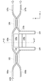
- FIG. 3 illustrates a configuration (plan view of the substrate) on the XZ plane of the optical signal processing device according to the first embodiment of the present invention.
- the optical signal processing device shown in FIG. 3 is an optical circuit of a PLC optical switch and constitutes a Mach-Zehnder interferometer (MZI).
- MZI Mach-Zehnder interferometer
- FIG. 3 an optical signal input from one (101a) of the left input waveguides 101a and 101b is split into an arm optical waveguide 103a and an arm optical waveguide 103b in a left 2-input 2-output directional coupler 102.
- the signals are waved, multiplexed in the right two-input two-output directional coupler 106, and output from the right output waveguides 107a and 107b according to the interference result.
- a heater 104 of a phase shifter as a phase modulation element is provided on the arm optical waveguide 103b, which is one of the two branched arm optical waveguides 103a and 103b, and heat insulation is provided on both sides of the arm optical waveguide 103b. Grooves 105a and 105b are provided. By supplying heat from the heater 104 of the phase shifter to the arm optical waveguide 103b, a phase change is given to the guided light of the arm waveguide by the thermo-optic effect to drive it as a phase modulation element (phase shifter). Also shown in FIG. 3 is electrical wiring 109 that supplies power to drive the heater 104 of the phase shifter. Although not shown in FIG. 3, a power supply for supplying electric power to the electric wiring 109 and a control unit for controlling the supply amount may be provided.
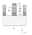
- FIG. 4 is a cross-sectional view of the substrate taken along the dotted line B-B′ in the first embodiment shown in FIG.
- the first silica film (112-1) is provided on the silicon substrate 110.
- a second silica film (112-2) formed by thermal oxidation is further present on the first silica film (112-1).
- Such a silica film layer can be realized by bonding substrates. The details of the method for producing a silica film layer by bonding such substrates are specifically described in Example 2.
- the optical waveguide core 111 is provided on the second silica film (112-2), and the second silica film (112-2) functions as an underclad.
- Overcladding 113 is formed on and around the optical waveguide core 111.
- a silica film is often used for the overclad as well, but it is sufficient if the refractive index is lower than that of the core, and therefore the surroundings may be etched to use air for the overclad.
- a heater 104 of a phase shifter is installed above the overclad 113.
- the clad on both sides of the core 111 may be etched to form the heat insulating grooves 105a and 105b.
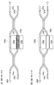
- FIG. 5 shows the basic operation of the MZI according to the first embodiment of the present invention.
- the heater of the phase shifter is energized to generate heat.
- the heater of the phase shifter is not energized and cools. It is in a state.
- the light input to the MZI is split into two arm optical waveguides 103a and 103b by the directional coupler on the input side, and after passing through each arm, is again output by the directional coupler on the output side. Combined. At this time, the output destination from the directional coupler on the output side changes due to the phase difference of light when the light is input from the two arms to the directional coupler on the output side.
- the refractive index of one arm of the MZI can be changed by driving the phase shifter, and the phase difference when inputting to the directional coupler on the output side can be adjusted.
- phase shifter uses the thermo-optical effect, heat is supplied to the MZI arm by the heater 104 or the like.
- the thermal conductivity of the silicon substrate is much higher than that of the core and the clad, and the volume of the silicon substrate is large. The heat escapes to the silicon substrate.
- the heat insulating grooves 105a and 105b are formed, and the diffusion direction of the heat supplied from the heater 104 of the phase shifter is limited to the Y direction toward the substrate 110.
- the longer the distance from the core to the silicon substrate having high thermal conductivity, that is, the thickness of the underclad (112-1, 112-2) is. The thicker the core, the higher the temperature of the core can be raised in the steady state for the same amount of heat supply, and thus the switching can be performed with less power.
- a thermally oxidized silica film with high film quality is a preferred silica film for undercladding, but there is a problem in increasing the film thickness. This is because the thermal oxidation silica film has a longer growth time per unit thickness (the growth rate decreases) as the silica film thickness increases. Since the decrease in the growth rate becomes more remarkable as the film thickness increases, a very long film forming time is required to form a thick film.
- the silicon substrate having the first silica film formed on the surface is bonded to another substrate on the side of the first silica film, and after polishing from the back surface of the silicon substrate, further heat treatment is performed.
- a second silica film is formed by oxidation.
- the total value of the silica film thicknesses existing up to the substrate is calculated as the total film thickness value of the first silica film and the second silica film while using the thermally oxidized silica film as the underclad immediately below the core.
- the first silica film it is not necessary for the first silica film to be a thermally oxidized silica film because the second silica film directly below the core has a strong effect on the core through which light passes as an underclad.
- the time required for growth is about half the thickness of the conventional single thermally oxidized silica film. It is possible to greatly reduce the length as compared with the conventional one.
- polishing or thermal oxidation is reduced to form a silicon layer between the first silica film (112-1) and the second silica film (112-2).
- the effect of the present invention is exhibited even with the structure in which 114 remains.
- the heat is discharged to the silicon substrate under the underclad in the Y direction, the Z direction which is the traveling axis of the guided light, and the first silica film and the second silica.
- the silicon layer 114 remaining between the films it also propagates in the X direction perpendicular to the direction of the arm. Since the X direction is etched and is in contact with air having a very poor thermal conductivity, the heat outflow can be ignored. In such a case, the easiness of heat outflow (propagation multiplier) depends on the cross-sectional area when the composition of the outflow path is the same. Heat can easily escape to a route with a wide cross-sectional area, and heat cannot escape easily with a narrow cross-sectional area.
- the cross-sectional area of the heat outflow path in the Z direction remains between the width of the ridge of the waveguide portion surrounded by the groove and the first silica film and the second silica film. It is the product of the thickness of the silicon layer 114, and the cross-sectional area of the heat outflow path in the Y direction is the product of the width of the ridge of the waveguide portion surrounded by the groove and the length of the phase shifter.
- the length of the phase shifter is on the order of millimeters, and if the thickness of the silicon layer 114 remaining between the first silica film and the second silica film is sufficiently smaller than this, the outflow from the path is prevented. The effect is limited and cannot be the dominant factor. Since the thickness of the silicon layer 114 may be set to a certain thickness or less, there is an advantage that the condition determination at the time of forming the thermally oxidized silica film is simplified.
- two or more silica films may be provided between the core 111 of the optical waveguide and the silicon substrate 110.
- One may be a thermally oxidized silica film formed by thermal oxidation.
- a silicon layer may be provided on at least one of the bonding interfaces between a plurality of silica films.
- the first silicon substrate is turned over and the surface of the first silica film is removed.
- the layer thickness of the silicon layer on the silica film is controlled by adhering to another second silicon substrate and grinding and polishing the back surface of the adhered first silicon substrate.
- the silicon layer remaining on the back surface of the first silicon substrate is further thermally oxidized to form the second silica film, whereby the thermally oxidized silica film to be the underclad can be formed in a short time.
- a silica film 112-1 is formed on the surface of the Si substrate 112-0.
- the silica film 112-1 may be a thermally oxidized silica film, but need not be a thermally oxidized silica film.
- the Si substrate 112-0 is turned upside down and bonded to the Si substrate 110 on the surface of the silica film 112-1.
- the Si substrate 112-0 on the upper surface (the lower surface and the back surface in FIG. 7A) of the Si substrate 112-0 which is turned over and bonded to the Si substrate 110 is desired by grinding/polishing. To the thickness of.
- the Si substrate 112-0 thinned by grinding and polishing is subjected to thermal oxidation treatment.
- the thermal oxidation process does not have to be performed up to the thickness of all Si substrates 112-0, and it is sufficient that the thermally oxidized silica film 112-2 having a desired thickness can be formed. If there is a remaining portion of the Si substrate 112-0 that has not been thermally oxidized, the silicon layer 114 of FIG. 6 is formed.
- FIG. 7D the thermally oxidized silica film 112-2 produced by the thermal oxidation treatment is completed on the silica film 112-1 produced in FIG. 7A.
- the silica film 112-1 and the thermally oxidized silica film 112-2, or the silica film 112-1 and the thermally oxidized silica film 112-2 sandwiching the silicon layer 114 become a thick silica film as a whole, and the thermally oxidized silica film 112-2 is formed. Becomes underclad.
- the optical waveguide core 111, the overclad 113, the heat insulating grooves 105a and 105b are formed, and the heater 104 of the phase shifter and the electric wiring 109 are attached to complete the PLC.
- the silica film 112-1 at the time of bonding does not have to be a film formed by thermal oxidation. Further, even when the silica film 112-1 is formed by thermal oxidation, if the thermal oxide film is formed in advance before the bonding, the manufacturing time of the PLC is not affected.
- a silica film is formed on the surface of the first silicon substrate, a thermally oxidized silica film is formed on the surface of the second silicon substrate, and the silica film surfaces of the first and second silicon substrates are formed. You may produce a thick silica film by sticking together. After that, the back surface of the second silicon substrate is ground and polished until the thermally oxidized silica film is exposed, and undercladding by thermally oxidized silica can be realized.
- the silica film formed by thermal oxidation can be formed with respect to the substrate thickness.
- the total silica film thickness can be increased.
- the drive power of the MZI can be reduced by the present invention, the power consumption can be reduced correspondingly in the case of an optical signal processing device that needs to drive many MZIs.
- Non-Patent Document 4 it is necessary to drive 2 ⁇ N MZIs in an M-input/N-output optical switch such as a PILOSS switch (Non-Patent Document 4) or a multicast switch (Non-Patent Document 5). Therefore, a large-scale switch has a problem that driving power also increases. (See Non-Patent Documents 4 and 5)
- a VOA (variable optical attenuator) array is another device that needs to drive many MZIs.
- MZI variable optical attenuator
- the output power of an optical signal is controlled by adjusting the phase shifter of MZI.
- optical filters can be realized by driving multiple MZIs.
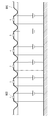
- FIG. 8 is a diagram illustrating an example of a lattice filter as the third embodiment of the present invention.
- FIG. 8 also shows an optical waveguide 801 which is an actual optical circuit on the optical waveguide substrate and a layout of electric wiring for controlling the phase shifters 802-1 to 802-1.
- the lattice filter has been described as an example in the third embodiment, it can be applied to a transversal filter, a filter using a ring resonator, a variable optical attenuator array using MZI, and an optical signal processing device combining them. It is clear that
- the power can be increased by increasing the underclad. It is possible to realize an optical signal processing device with reduced consumption, and to realize a manufacturing method in which the time for forming the thermally oxidized silica film immediately below the optical waveguide core is shortened in manufacturing the optical signal processing device.
Landscapes
- Physics & Mathematics (AREA)
- Nonlinear Science (AREA)
- General Physics & Mathematics (AREA)
- Optics & Photonics (AREA)
- Engineering & Computer Science (AREA)
- Health & Medical Sciences (AREA)
- Manufacturing & Machinery (AREA)
- Ophthalmology & Optometry (AREA)
- Mechanical Engineering (AREA)
- Optical Modulation, Optical Deflection, Nonlinear Optics, Optical Demodulation, Optical Logic Elements (AREA)
- Optical Integrated Circuits (AREA)
Abstract
シリカPLCのアンダークラッドに熱酸化シリカ膜を使用しつつ、アンダークラッドの厚みを厚くし、かつ製造時に成膜時間を短くすることが可能な光信号処理装置を実現する。シリコン基板上に形成された光導波路を含む平面光回路として形成され、熱光学効果を用いた位相変調素子を有する光信号処理装置であって、光導波路のコアとシリコン基板の間に複数のシリカ膜を有しており、前記複数のシリカ膜のうち少なくとも一つが熱酸化により形成されていることを特徴とする光信号処理装置とした。
Description
本発明は、光信号処理装置および光信号処理装置の製造方法に関する。
従来、シリカ(二酸化シリコン、SiO2)材料を用いた平面光回路(Planar Lightwave Circuit: PLC)で構成された光信号処理装置は、光通信において重要な役割を担うデバイスとなっている。シリカPLCでは、数~数十μmという非常に小さな光導波路に光を閉じ込めることができ、小さなチップでさまざまな機能を発現する光信号処理装置を構成することができる。シリカPLCを用いた光スイッチも、チップにその機能を集積することが可能であり、その制御は電気信号による熱光学効果を用いて実現される。
図1に、従来の光信号処理装置の一例として、PLC光スイッチの光回路を模式的に示す。この光回路は、マッハツェンダー干渉計(MZI)を構成しており、左の入力導波路1a、1bの一方(例えば1a)から入力された光信号は、左の2入力2出力の方向性結合器2において、アーム光導波路3a、3bに分波され、右の2入力2出力の方向性結合器6において合波され、干渉した結果に応じて右の出力導波路7a、7bから出力される。
分岐した2本のアーム光導波路の片方の、アーム光導波路3bの上には、位相変調素子としての位相シフタのヒータ4が設けられ、またアーム光導波路3bの両脇には断熱溝5a、5bが設けられている。位相シフタのヒータ4に通電してアーム光導波路3bに熱を供給することで、熱光学効果によりアーム導波路3bの導波光に位相変化を与えて、位相変調素子(位相シフタ)として駆動する。(例えば、特許文献1参照)。
シリカPLCスイッチの駆動に必要な電力は、位相変調素子(位相シフタ)のヒータ4の駆動電力である。図1に記載した光スイッチでは、位相シフタのヒータ4により下層のアーム光導波路3bを加熱することで加熱された部分の屈折率を変化させ、導波光の位相を変調する。図1のMZI回路では、上下のアーム導波路を通る光の位相差に応じて方向性結合器6における干渉条件が変化し、2つの出力導波路7a、7bの出力光強度が変化するため、この位相変調素子の制御により光スイッチング機能を実現することができる。
図2に、図1の位相変調素子(位相シフタ)の領域の、断面A-A’の基板断面図を示す。図2で、Si基板10の上に形成された光導波路3bは、コア11と呼ばれる光が閉じ込められる領域の上下を、クラッド(アンダークラッド12、オーバークラッド13)と呼ばれる領域が挟んで構成されており、位相変調素子の領域のオーバークラッド13の上には位相シフタのヒータ4が設けられている。
シリカPLCでは、通常コアとクラッドはともにシリカが使用される。ヒータ4から供給される熱により、コア11の温度を制御することで導波光の位相変調を行うことができる。ヒータ4からの熱をコア11に効率的に伝えるため、コアの両サイドのクラッドをエッチングで削り、断熱溝5a,5bを形成することで、効率的に熱をコアに届けることができる。
シリカPLCでは一般的に、基板10にSi(シリコン)を用いることが多い。Siはシリカと比較して熱伝導率が高いため、最終的にヒータ4から供給される熱はSi基板10に逃げていく。加熱時の定常状態では、ヒータ4とSi基板10の間の温度勾配により、Si基板10へ逃げる熱量とヒータ4から供給される熱量が等しくなる。そのため、コア11と基板10の間のクラッド(アンダークラッド12)が厚ければ厚いほど、コアは熱が逃げるSi基板から離れるため、ヒータからの熱供給量が同一であっても高い温度にすることができる。よって、アンダークラッドを厚くすることで、シリカPLCスイッチは低消費電力化することができる。
T. Shibata et al., "Silica-Based Waveguide-Type 16 x 16 Optical Switch Module Incorporating Driving Circuits", in IEEE Photonics Technology Letters, vol. 15, no. 9, pp. 1300-1302, Sept. 2003.
山部 紀久夫,蓮沼 隆,極薄シリコン酸化膜における原子レベルの膜厚均一性と信頼性,Journal of the Vacuum Society of Japan,2015,VOL.58,NO.1,p-p. 27-34
古川 和由, シリコンウェハの直接接合, 溶接学会誌, 1990, VOL.59, NO.2, p-p 105-109
Takashi Goh et al., "High-Extinction Ratio and Low-Loss Silica-Based 8x8 Strictly Nonblocking Thermooptic Matrix Switch", J. Lightwave Technology. VOL.17, NO.7, p-p 1192-1199, JULY 1999.
T. Watanabe et. al., "Silica-based PLC Transponder Aggregateors for Colorless, Directionless, and Contentionless ROADM", OFC/NFOEC2012, OTh3D.1, March 8, 2012, Los Angeles
Kei Watanabe et. al., "Ultralow Power Consumption Silica-Based PLC-VOA/Switches", J. Lightwave Technol. VOL.26, NO.14, JULY 2008, p-p 2235-2244
Si基板上にシリカを形成する方法として、CVD(Chemical Vapor Deposition)法や熱酸化法があるが、熱酸化法ではフラットネスが高く品質の良いシリカ膜が形成できることが知られている。(非特許文献2参照)
しかしながら、熱酸化によって厚いシリカ膜を形成するためには、周辺雰囲気中の酸素分子がすでに形成されたシリカ膜を抜けてSi基板に届く必要があり、厚くなればなるほど熱酸化シリカ膜の成長には時間がかかる。そのため、光スイッチのような光信号処理装置の消費電力を下げるためにシリカPLCのアンダークラッドとして熱酸化シリカ膜を使用し、かつ厚いシリカ膜とするためには、作製に必要な時間とコストが増大することが問題となる。
本発明は、このような問題を解決するためになされたものである。その目的とするところは、シリカPLCのアンダークラッドに熱酸化シリカ膜を使用しつつ、アンダークラッドの厚みを厚くし、かつ製造時に成膜時間を短くすることが可能な光信号処理装置の実現、およびそのような光信号処理装置の製造方法の実現にある。
本発明は、このような目的を達成するために、以下のような構成としている。
シリコン基板上に形成された光導波路を含む平面光回路として形成され、熱光学効果を用いた位相変調素子を有する光信号処理装置であって、熱酸化シリカ膜を有する基板と、シリカ膜を有する基板を貼り合わせた構成として、光導波路コアのアンダークラッドとして熱酸化シリカ膜を使用した構成としている。
シリコン基板上に形成された光導波路を含む平面光回路として形成され、熱光学効果を用いた位相変調素子を有する光信号処理装置であって、熱酸化シリカ膜を有する基板と、シリカ膜を有する基板を貼り合わせた構成として、光導波路コアのアンダークラッドとして熱酸化シリカ膜を使用した構成としている。
本発明は、具体的には、以下のような構成を備えることを特徴とする。
(構成1)
シリコン基板上に形成された光導波路を含む平面光回路として形成され、熱光学効果を用いた位相変調素子を有する光信号処理装置であって、
光導波路のコアとシリコン基板の間に複数のシリカ膜を有しており、
前記複数のシリカ膜のうち少なくとも一つが熱酸化により形成されている
ことを特徴とする光信号処理装置。
シリコン基板上に形成された光導波路を含む平面光回路として形成され、熱光学効果を用いた位相変調素子を有する光信号処理装置であって、
光導波路のコアとシリコン基板の間に複数のシリカ膜を有しており、
前記複数のシリカ膜のうち少なくとも一つが熱酸化により形成されている
ことを特徴とする光信号処理装置。
(構成2)
前記複数のシリカ膜同士の界面のうち、少なくとも一つの界面にシリコン層を有する
ことを特徴とする構成1の光信号処理装置。
前記複数のシリカ膜同士の界面のうち、少なくとも一つの界面にシリコン層を有する
ことを特徴とする構成1の光信号処理装置。
(構成3)
複数の基板の貼り合わせにより前記シリコン基板とシリカ膜が作製されている
ことを特徴とする構成1または2に記載の光信号処理装置。
複数の基板の貼り合わせにより前記シリコン基板とシリカ膜が作製されている
ことを特徴とする構成1または2に記載の光信号処理装置。
(構成4)
前記光導波路がマッハツェンダー干渉計を形成している
ことを特徴とする構成1から3のいずれか1項に記載の光信号処理装置。
前記光導波路がマッハツェンダー干渉計を形成している
ことを特徴とする構成1から3のいずれか1項に記載の光信号処理装置。
(構成5)
前記光信号処理装置が、マトリックススイッチ、マルチキャストスイッチ、または光フィルタもしくは光信号減衰器の機能を有する
ことを特徴とする構成1から4のいずれか1項に記載の光信号処理装置。
前記光信号処理装置が、マトリックススイッチ、マルチキャストスイッチ、または光フィルタもしくは光信号減衰器の機能を有する
ことを特徴とする構成1から4のいずれか1項に記載の光信号処理装置。
(構成6)
第1のシリコン基板の表面に第1のシリカ膜を形成するステップと、
第1のシリコン基板を第1のシリカ膜の面で別の第2のシリコン基板と張り合わせるステップと、
張り合わせた第1のシリコン基板の裏面を研削・研磨するステップと、
研削・研磨された第1のシリコン基板の裏面のシリコン層を熱酸化して熱酸化シリカによるアンダークラッドを形成するステップと、
を備えることを特徴とする光信号処理装置の製造方法。
第1のシリコン基板の表面に第1のシリカ膜を形成するステップと、
第1のシリコン基板を第1のシリカ膜の面で別の第2のシリコン基板と張り合わせるステップと、
張り合わせた第1のシリコン基板の裏面を研削・研磨するステップと、
研削・研磨された第1のシリコン基板の裏面のシリコン層を熱酸化して熱酸化シリカによるアンダークラッドを形成するステップと、
を備えることを特徴とする光信号処理装置の製造方法。
(構成7)
第1のシリコン基板の表面にシリカ膜を形成するステップと、
第2のシリコン基板の表面に熱酸化シリカ膜を形成するステップと、
第1のシリコン基板のシリカ膜と、第2のシリコン基板の熱酸化シリカ膜の面を貼り合わせるステップと、
第2のシリコン基板の裏面を熱酸化シリカ膜が露出するまで研削・研磨して、熱酸化シリカによるアンダークラッドを形成するステップと、
を備える光信号処理装置の製造方法。
第1のシリコン基板の表面にシリカ膜を形成するステップと、
第2のシリコン基板の表面に熱酸化シリカ膜を形成するステップと、
第1のシリコン基板のシリカ膜と、第2のシリコン基板の熱酸化シリカ膜の面を貼り合わせるステップと、
第2のシリコン基板の裏面を熱酸化シリカ膜が露出するまで研削・研磨して、熱酸化シリカによるアンダークラッドを形成するステップと、
を備える光信号処理装置の製造方法。
(構成8)
アンダークラッドの上に光導波路コアおよびオーバークラッドを形成するステップと、
位相変調素子の光導波路の両脇に断熱溝を形成し、位相変調素子の位相シフタのヒータと電気配線を取り付けるステップと、
をさらに備える構成6または7に記載の光信号処理装置の製造方法。
アンダークラッドの上に光導波路コアおよびオーバークラッドを形成するステップと、
位相変調素子の光導波路の両脇に断熱溝を形成し、位相変調素子の位相シフタのヒータと電気配線を取り付けるステップと、
をさらに備える構成6または7に記載の光信号処理装置の製造方法。
本発明によれば、光導波路とヒータを利用した位相変調素子を用いて実現される光スイッチや光フィルタ等の光信号処理装置のPLCにおいて、アンダークラッドを厚くすることで電力消費量を削減した光信号処理装置を実現でき、またその製造に際して光導波路コア直下の熱酸化シリカ膜成膜時間を短縮した製造方法を実現することができる。
以下、図面を参照しながら本発明の実施形態について詳細に説明する。
図3に本発明の実施例1の光信号処理装置のX-Z面の構成(基板平面図)を図示する。図3の光信号処理装置は、PLC光スイッチの光回路であり、マッハツェンダー干渉計(MZI)を構成している。図3において、左の入力導波路101a、101bの一方(101a)から入力された光信号は、左の2入力2出力の方向性結合器102において、アーム光導波路103a、アーム光導波路103bに分波され、右の2入力2出力の方向性結合器106において合波され、干渉した結果に応じて右の出力導波路107a、107bから出力される。
分岐した2本のアーム光導波路103a、103bのうち片方の、アーム光導波路103bの上には、位相変調素子としての位相シフタのヒータ104が設けられ、またアーム光導波路103bの両脇には断熱溝105a、105bが設けられている。位相シフタのヒータ104からアーム光導波路103bに熱を供給することで、熱光学効果によりアーム導波路の導波光に位相変化を与えて位相変調素子(位相シフタ)として駆動する。図3にはまた、位相シフタのヒータ104を駆動する電力を供給する電気配線109も示されている。図3には記載しないが、電気配線109に電力を供給する電源や供給量を制御する制御部があってもよい。
また、図4は、図3の実施例1における点線B-B’の部分の基板断面図である。
本実施例1の構成では、シリコン基板110の上に第1のシリカ膜(112-1)を有する。第1のシリカ膜(112-1)上にはさらに、熱酸化で成膜された第2のシリカ膜(112-2)が存在する。このようなシリカ膜層は、基板の貼り合わせにより実現することが可能である。このような基板の貼り合わせによるシリカ膜層の製造方法の詳細は、具体的には実施例2に記載している。
また、第2のシリカ膜(112-2)の上に光導波路コア111を有しており、第2のシリカ膜(112-2)がアンダークラッドとして機能している。光導波路コア111の上部と周囲にはオーバークラッド113が形成されている。オーバークラッドにもシリカ膜が使用されることが多いが、コアよりも屈折率が低ければ良いため、周囲をエッチングして空気をオーバークラッドに活用しても構わない。オーバークラッド113の上部には位相シフタのヒータ104が設置されている。コア111の両サイドのクラッドをエッチングで削り、断熱溝105a,105bを形成してもよい。
図5に、本発明の実施例1のMZIの基本動作を示す。図5(a)の位相シフタONの状態では、位相シフタのヒータが通電されて発熱状態であり、図5(b)の位相シフタOFFの状態では、位相シフタのヒータが通電されずに冷えた状態である。
図5で、MZIに入力された光は、入力側の方向性結合器により2つのアーム光導波路103a、103bに分岐し、それぞれのアームを通ったのちに再度、出力側の方向性結合器によって合波される。この時、2つのアームから出力側の方向性結合器に入力する際の光の位相差により、出力側の方向性結合器からの出力先が変化する。
本構成の光信号処理装置では、位相シフタを駆動することによりMZIの片側のアームの屈折率を変化させ、出力側の方向性結合器に入力する際の位相差を調整することができる。
位相シフタでは熱光学効果を使用するため、ヒータ104などによりMZIのアームに熱を供給する。シリコン基板上に導波路を形成し、コアやクラッドにシリカ膜を使用する場合にはコアやクラッドと比較してシリコン基板の熱伝導率の方が非常に高く、かつシリコン基板の体積が大きいためにシリコン基板に熱が逃げていく。
本構成では断熱溝105a、105bを形成しており、位相シフタのヒータ104から供給される熱の拡散方向は、基板110に向かうY方向に限られる。この場合、供給する熱により温度を上げたいのはコア111であるため、コアから熱伝導率の高いシリコン基板までの距離が長いほど、つまりアンダークラッド(112-1、112-2)の厚みが厚いほど同量の熱供給量に対して定常状態でのコアの温度を上げることができるため、少ない電力でスイッチングを行うことができる。
先に述べたが、膜質の高い熱酸化シリカ膜はアンダークラッドとして好ましいシリカ膜であるが、厚膜化に課題がある。これは、熱酸化シリカ膜は、シリカ膜厚が厚くなるほど単位厚さあたりの成長時間が長くなる(成長速度が低下する)ことによる。この成長速度の低下は膜厚が厚くなるほど顕著になるため、厚い膜の形成には非常に長い成膜時間が必要になる。
これに対し、本実施例1の構成では、表面に第1のシリカ膜を形成したシリコン基板を、第1のシリカ膜の側で別の基板に張り合わせ、シリコン基板の裏面から研磨後、更に熱酸化により第2のシリカ膜を形成する。これにより、コア直下のアンダークラッドとして熱酸化シリカ膜を使用しつつ、基板までの間に存在するシリカ膜厚の合計値を、第1のシリカ膜と第2のシリカ膜の膜厚の合計値とすることができる。
このようなシリカ膜形成後の張り合わせはSOI(Silicon on Insulator)基板等の作製で行われており、これらの一般的な手法が活用可能である。(非特許文献3参照)
この時、アンダークラッドとして光が通るコアへと強い影響を与えるのはコア直下にある第2のシリカ膜であるため、第1のシリカ膜は熱酸化シリカ膜でなくても構わない。
もし第1のシリカ膜および第2のシリカ膜の両方で熱酸化シリカ膜を使用したとしても、従来の単独の熱酸化シリカ膜の厚さの半分程度であるから、成長に必要とする時間は従来に比較して大幅に短縮することが可能である。
また、図6の実施例1の別構成のように、研磨または熱酸化を少なくして、第1のシリカ膜(112-1)と第2のシリカ膜(112-2)の間にシリコン層114の残った構成であっても、本発明の効果は発揮される。
この図6の別構成のような場合、熱が流出する先は、アンダークラッド下のシリコン基板というY方向に加え、導波光の進行軸であるZ方向および第1のシリカ膜と第2のシリカ膜の間に残ったシリコン層114を通じてアームの通る方向に直角なX方向にも伝搬する。X方向はエッチングしてあり、熱伝導率の非常に悪い空気と接しているため、熱の流出を無視することができる。このような場合、熱の流出のしやすさ(伝搬乗数)は、流出経路の組成が同じ場合には断面積に依存する。広い断面積を持つ経路には熱が逃げやすく、狭い断面積では熱が逃げにくい。
図6の別構成の場合、Z方向への熱流出経路の断面積は、溝に囲まれた導波路部のリッジの幅と、第1のシリカ膜および第2のシリカ膜の間に残ったシリコン層114の厚みの積であり、Y方向への熱流出経路の断面積は、溝に囲まれた導波路部のリッジの幅と位相シフタの長さの積である。
通常、位相シフタの長さはミリメータのオーダであり、第1のシリカ膜および第2のシリカ膜の間に残ったシリコン層114の厚みがこれよりも十分薄ければ、その経路からの流出の効果は限定的なものになり、支配的な要因にはなりえない。シリコン層114の厚みは、ある一定以下の厚みにすればよいため、熱酸化シリカ膜成膜時の条件決めが簡易になる等のメリットがある。
また、2以上の複数のシリコン基板を張り合わせることにより、光導波路のコア111とシリコン基板110の間に、2以上の複数のシリカ膜を有していてもよく、複数のシリカ膜のうち少なくとも一つが熱酸化により形成された熱酸化シリカ膜であればよい。
またさらに、複数のシリカ膜同士の張り合わせ界面のうち、少なくとも一つの界面にシリコン層を有していてもよい。
このような構成でアンダークラッドを形成することで、PLC光スイッチとしてMZIの出力先の切り替えを低い電力で実現しつつ、トータルの製造時間を削減することが可能である。
(光信号処理装置の製造方法)
実施例1の説明において、熱酸化シリカ膜をアンダークラッドにしつつ、シリコン基板までのシリカ膜厚を厚くするため、基板の張り合わせを行う構造が、光信号処理装置の低消費電力化および製造時間の短縮に有効であることを説明した。
実施例1の説明において、熱酸化シリカ膜をアンダークラッドにしつつ、シリコン基板までのシリカ膜厚を厚くするため、基板の張り合わせを行う構造が、光信号処理装置の低消費電力化および製造時間の短縮に有効であることを説明した。
本発明の実施例2として、光信号処理装置の製造方法を説明する。特に、基板の張り合わせの方法について図7を参照して詳細に説明する。
実施例2の光信号処理装置の製造方法では、概略、第1のシリコン基板の表面に第1のシリカ膜を形成した後で、第1のシリコン基板を裏返して第1のシリカ膜の面で別の第2のシリコン基板と張り合わせ、張り合わせた第1のシリコン基板の裏面を研削・研磨することで、シリカ膜上のシリコン層の層厚を制御する。
その後、第1のシリコン基板の裏面に残ったシリコン層をさらに熱酸化して第2のシリカ膜を形成することにより、アンダークラッドとなる熱酸化シリカ膜を短時間で形成することができる。
この実施例2の製造方法の詳細フローを、図7(a)~(d)に示す。
まず図7(a)のように、2枚のSi基板110と112-0を用意して、Si基板112-0の表面にシリカ膜112-1を形成しておく。シリカ膜112-1は熱酸化シリカ膜であってもよいが、熱酸化シリカ膜でなくてもかまわない。そしてSi基板112-0を裏返して、シリカ膜112-1の面でSi基板110と張り合わせる。
次に図7(b)のように、裏返してSi基板110と張り合わせたSi基板112-0の上面(図7(a)における下面、裏面)のSi基板112-0を、研削・研磨により所望の厚みまで薄層化する。
図7(c)では、研削・研磨により薄層化したSi基板112-0を、熱酸化処理する。熱酸化処理は、全てのSi基板112-0の厚みまで行う必要は無く、所望の厚みの熱酸化シリカ膜112-2が形成できればよい。熱酸化されなかったSi基板112-0の残り部分がある場合は、図6のシリコン層114となる。
図7(d)では、熱酸化処理により生成された熱酸化シリカ膜112-2が、図7(a)で作成したシリカ膜112-1の上に完成している。シリカ膜112-1と熱酸化シリカ膜112-2、またはシリコン層114を挟んだシリカ膜112-1と熱酸化シリカ膜112-2が、全体として厚いシリカ膜となり、熱酸化シリカ膜112-2がアンダークラッドとなる。
以後、光導波路コア111、オーバークラッド113、断熱溝105a,105bを形成して、位相シフタのヒータ104や電気配線109を取り付けてPLCの完成となる。
この時、張り合わせる際のシリカ膜112-1は、熱酸化による成膜でなくても問題ないことは、実施例1の説明で既に述べた。また、シリカ膜112-1を熱酸化による成膜とする場合でも、張り合わせる際に先んじて予め熱酸化膜を形成しておけば、PLCの製造時間には影響はしない。
他の製造方法としては、第1のシリコン基板の表面にシリカ膜を形成し、第2のシリコン基板の表面に熱酸化シリカ膜を形成し、第1および第2のシリコン基板のシリカ膜の面同士を貼り合わせることで厚いシリカ膜を作製してもよい。そののちに第2のシリコン基板の裏面を熱酸化シリカ膜が露出するまで研削・研磨して、熱酸化シリカによるアンダークラッドを実現できる。
上記のように張り合わせや成膜方法は複数考えられるが、本発明では成膜を別に行ったシリカを有する基板を貼り合わせることで、熱酸化で成膜するシリカ膜厚に対して、基板までのシリカ膜厚の総膜厚を厚くすることができる。
本発明によりMZIの駆動電力を小さくできるため、多くのMZIを駆動する必要のある光信号処理装置であれば、それだけ電力消費量を削減できる。
例えば、PILOSSスイッチ(非特許文献4)やマルチキャストスイッチ(非特許文献5)のM入力N出力光スイッチでは、2×N個のMZIを駆動する必要がある。そのため、大規模なスイッチになると駆動電力も大きくなることが課題となる。(非特許文献4、5参照)
本発明により各MZIを駆動するための電力を削減することができる為、デバイス全体の電力削減効果も大きなものになる。
多くのMZIを駆動する必要のあるデバイスとして、VOA(variable optical attenuator)アレイも挙げられる。(非特許文献6参照)MZIを用いたVOAでは、MZIの位相シフタの調整により、光信号の出力パワーを制御する。MZIをアレイ化することで、一つのデバイスで多くの光信号の強度を独立して制御することが可能になる。しかし全てのMZIを駆動する必要があり、アレイ数に比例して消費電力は増えていくことが課題であった。このような場合にも、MZIの消費電力を下げる事ができる本発明は有効な解決手段となる。
さらに、光フィルタでも複数のMZIを駆動することで実現するものがある。
図8は、本発明の実施例3としてラティスフィルタの例を説明する図である。図8には光導波路基板上の実際の光回路となる光導波路801、および位相シフタ802-1~6を制御する電気配線のレイアウトも記載している。
また、本実施例3では、ラティスフィルタを例として説明したが、トランスバーサルフィルタやリング共振器によるフィルタ、MZIを用いる可変光減衰器アレイや、さらにはそれらを組み合わせた光信号処理装置に適用可能であることは明らかである。
以上のように、本発明によれば、光導波路とヒータを利用した位相変調素子を用いて実現される光スイッチや光フィルタ等の光信号処理装置のPLCにおいて、アンダークラッドを厚くすることで電力消費量を削減した光信号処理装置を実現でき、またその製造に際して光導波路コア直下の熱酸化シリカ膜の成膜時間を短縮した製造方法を実現することができる。
1a、1b、101a、101b 入力導波路
2、6、102、106 方向性結合器
3a、3b、103a、103b アーム光導波路
7a、7b、107a、107b 出力導波路
4、104 位相シフタのヒータ
5a、5b、105a、105b 断熱溝
10,110、112-0 Si基板
11、111 コア
12 アンダークラッド
112-1 シリカ膜
112-2 熱酸化シリカ膜
13、113 オーバークラッド
114 シリコン層
109 電気配線
2、6、102、106 方向性結合器
3a、3b、103a、103b アーム光導波路
7a、7b、107a、107b 出力導波路
4、104 位相シフタのヒータ
5a、5b、105a、105b 断熱溝
10,110、112-0 Si基板
11、111 コア
12 アンダークラッド
112-1 シリカ膜
112-2 熱酸化シリカ膜
13、113 オーバークラッド
114 シリコン層
109 電気配線
Claims (8)
- シリコン基板上に形成された光導波路を含む平面光回路として形成され、熱光学効果を用いた位相変調素子を有する光信号処理装置であって、
光導波路のコアとシリコン基板の間に複数のシリカ膜を有しており、
前記複数のシリカ膜のうち少なくとも一つが熱酸化により形成されている
ことを特徴とする光信号処理装置。 - 前記複数のシリカ膜同士の界面のうち、少なくとも一つの界面にシリコン層を有する
ことを特徴とする請求項1に記載の光信号処理装置。 - 複数の基板の貼り合わせにより前記シリコン基板とシリカ膜が作製されている
ことを特徴とする請求項1または2に記載の光信号処理装置。 - 前記光導波路がマッハツェンダー干渉計を形成している
ことを特徴とする請求項1から3のいずれか1項に記載の光信号処理装置。 - 前記光信号処理装置が、マトリックススイッチ、マルチキャストスイッチ、または光フィルタもしくは光信号減衰器の機能を有する
ことを特徴とする請求項1から4のいずれか1項に記載の光信号処理装置。 - 第1のシリコン基板の表面に第1のシリカ膜を形成するステップと、
第1のシリコン基板を第1のシリカ膜の面で別の第2のシリコン基板と張り合わせるステップと、
張り合わせた第1のシリコン基板の裏面を研削・研磨するステップと、
研削・研磨された第1のシリコン基板の裏面のシリコン層を熱酸化して熱酸化シリカによるアンダークラッドを形成するステップと、
を備えることを特徴とする光信号処理装置の製造方法。 - 第1のシリコン基板の表面にシリカ膜を形成するステップと、
第2のシリコン基板の表面に熱酸化シリカ膜を形成するステップと、
第1のシリコン基板のシリカ膜と、第2のシリコン基板の熱酸化シリカ膜の面を貼り合わせるステップと、
第2のシリコン基板の裏面を熱酸化シリカ膜が露出するまで研削・研磨して、熱酸化シリカによるアンダークラッドを形成するステップと、
を備える光信号処理装置の製造方法。 - アンダークラッドの上に光導波路コアおよびオーバークラッドを形成するステップと、
位相変調素子の光導波路の両脇に断熱溝を形成し、位相変調素子の位相シフタのヒータと電気配線を取り付けるステップと、
をさらに備える請求項6または7に記載の光信号処理装置の製造方法。
Priority Applications (1)
| Application Number | Priority Date | Filing Date | Title |
|---|---|---|---|
| US17/311,959 US12032231B2 (en) | 2018-12-26 | 2019-12-24 | Optical signal processing apparatus and manufacturing method thereof |
Applications Claiming Priority (2)
| Application Number | Priority Date | Filing Date | Title |
|---|---|---|---|
| JP2018-243258 | 2018-12-26 | ||
| JP2018243258A JP7119990B2 (ja) | 2018-12-26 | 2018-12-26 | 光信号処理装置 |
Publications (1)
| Publication Number | Publication Date |
|---|---|
| WO2020138053A1 true WO2020138053A1 (ja) | 2020-07-02 |
Family
ID=71125959
Family Applications (1)
| Application Number | Title | Priority Date | Filing Date |
|---|---|---|---|
| PCT/JP2019/050556 Ceased WO2020138053A1 (ja) | 2018-12-26 | 2019-12-24 | 光信号処理装置および光信号処理装置の製造方法 |
Country Status (3)
| Country | Link |
|---|---|
| US (1) | US12032231B2 (ja) |
| JP (1) | JP7119990B2 (ja) |
| WO (1) | WO2020138053A1 (ja) |
Families Citing this family (1)
| Publication number | Priority date | Publication date | Assignee | Title |
|---|---|---|---|---|
| JP7820668B2 (ja) * | 2022-06-15 | 2026-02-26 | Ntt株式会社 | シリコンフォトニクス回路及びシリコンフォトニクス回路の製造方法 |
Citations (7)
| Publication number | Priority date | Publication date | Assignee | Title |
|---|---|---|---|---|
| JPH10104451A (ja) * | 1996-09-30 | 1998-04-24 | Shin Etsu Chem Co Ltd | 光導波路用基板及びその作製方法 |
| JP2001051144A (ja) * | 1999-08-17 | 2001-02-23 | Nippon Telegr & Teleph Corp <Ntt> | 光導波路及びその作製方法 |
| JP2002162526A (ja) * | 2000-11-24 | 2002-06-07 | Shin Etsu Chem Co Ltd | 光導波路およびその製造方法 |
| US20030040135A1 (en) * | 2001-08-27 | 2003-02-27 | Trammel Pamela S. | Planar lightwave circuit active device metallization process |
| JP2004045453A (ja) * | 2002-07-08 | 2004-02-12 | Sumitomo Electric Ind Ltd | 導波路型光部品およびその製造方法 |
| JP2004085868A (ja) * | 2002-08-27 | 2004-03-18 | Matsushita Electric Ind Co Ltd | 光導波路デバイスおよびその製造方法 |
| JP2017142423A (ja) * | 2016-02-12 | 2017-08-17 | 古河電気工業株式会社 | 基板、光導波路素子、基板の製造方法、および光導波路素子の製造方法 |
Family Cites Families (4)
| Publication number | Priority date | Publication date | Assignee | Title |
|---|---|---|---|---|
| JP3796183B2 (ja) | 2002-02-26 | 2006-07-12 | 三菱電機株式会社 | 石英系光導波路部品 |
| EP1769275A1 (en) | 2004-07-22 | 2007-04-04 | Pirelli & C. S.p.A. | Integrated wavelength selective grating-based filter |
| WO2008111407A1 (ja) * | 2007-03-09 | 2008-09-18 | Nec Corporation | 熱光学位相シフタ |
| US9964702B1 (en) * | 2016-10-13 | 2018-05-08 | Oracle International Corporation | Surface-normal optical coupling interface with thermal-optic coefficient compensation |
-
2018
- 2018-12-26 JP JP2018243258A patent/JP7119990B2/ja active Active
-
2019
- 2019-12-24 WO PCT/JP2019/050556 patent/WO2020138053A1/ja not_active Ceased
- 2019-12-24 US US17/311,959 patent/US12032231B2/en active Active
Patent Citations (7)
| Publication number | Priority date | Publication date | Assignee | Title |
|---|---|---|---|---|
| JPH10104451A (ja) * | 1996-09-30 | 1998-04-24 | Shin Etsu Chem Co Ltd | 光導波路用基板及びその作製方法 |
| JP2001051144A (ja) * | 1999-08-17 | 2001-02-23 | Nippon Telegr & Teleph Corp <Ntt> | 光導波路及びその作製方法 |
| JP2002162526A (ja) * | 2000-11-24 | 2002-06-07 | Shin Etsu Chem Co Ltd | 光導波路およびその製造方法 |
| US20030040135A1 (en) * | 2001-08-27 | 2003-02-27 | Trammel Pamela S. | Planar lightwave circuit active device metallization process |
| JP2004045453A (ja) * | 2002-07-08 | 2004-02-12 | Sumitomo Electric Ind Ltd | 導波路型光部品およびその製造方法 |
| JP2004085868A (ja) * | 2002-08-27 | 2004-03-18 | Matsushita Electric Ind Co Ltd | 光導波路デバイスおよびその製造方法 |
| JP2017142423A (ja) * | 2016-02-12 | 2017-08-17 | 古河電気工業株式会社 | 基板、光導波路素子、基板の製造方法、および光導波路素子の製造方法 |
Non-Patent Citations (1)
| Title |
|---|
| BAUTERS. J. F. ET AL.: "Planar waveguides with less than 0.1 dB/m propagation loss fabricated with wafer bonding", OPTICS EXPRESS, vol. 19, no. 24, 21 November 2011 (2011-11-21), pages 24090 - 24100, XP055721817 * |
Also Published As
| Publication number | Publication date |
|---|---|
| JP2020106608A (ja) | 2020-07-09 |
| US20220066244A1 (en) | 2022-03-03 |
| US12032231B2 (en) | 2024-07-09 |
| JP7119990B2 (ja) | 2022-08-17 |
Similar Documents
| Publication | Publication Date | Title |
|---|---|---|
| Pintus et al. | Broadband TE optical isolators and circulators in silicon photonics through Ce: YIG bonding | |
| CN100405202C (zh) | 干涉仪型光开关和可变光衰减器 | |
| US5418868A (en) | Thermally activated optical switch | |
| JP2856880B2 (ja) | 偏光無依存性光スイッチ/変調器及びその製造方法 | |
| US5623566A (en) | Network with thermally induced waveguide | |
| JPH04213406A (ja) | 光導波管及びその製造方法 | |
| Kasahara et al. | New structure of silica-based planar lightwave circuits for low-power thermooptic switch and its application to 8× 8 optical matrix switch | |
| WO2003100507A1 (en) | Induced optical waveguide device | |
| JP3868122B2 (ja) | 熱光学光変調器 | |
| JP2020187173A (ja) | 位相シフタおよびその制御方法 | |
| JP6023680B2 (ja) | フェーズアレイ型光スイッチ | |
| JP7119990B2 (ja) | 光信号処理装置 | |
| JP2007212787A (ja) | 光制御素子、光スイッチングユニットおよび光変調器 | |
| JP4934614B2 (ja) | 熱光学位相シフタ | |
| JPH0534525A (ja) | 光回路 | |
| US6529647B2 (en) | Optical device with optical waveguides and manufacturing method therefor | |
| JP4638749B2 (ja) | 熱光学位相変調器及びその製造方法 | |
| JP4267888B2 (ja) | 光回路および光回路装置ならびに光回路の製造方法 | |
| JP2015191111A (ja) | 光分岐挿入装置、光スイッチおよび製造方法 | |
| JP2006259104A (ja) | 光回路及び導波路型光可変減衰器 | |
| JP2003029219A (ja) | 平面導波路型可変光減衰器 | |
| JP3573332B2 (ja) | 干渉型熱光学光部品 | |
| JP2008299238A (ja) | 導波路型光スイッチ | |
| WO2005069071A1 (ja) | 電気光学デバイス及びその製造方法 | |
| JP2004170657A (ja) | 導波路型光可変減衰器 |
Legal Events
| Date | Code | Title | Description |
|---|---|---|---|
| 121 | Ep: the epo has been informed by wipo that ep was designated in this application |
Ref document number: 19905018 Country of ref document: EP Kind code of ref document: A1 |
|
| NENP | Non-entry into the national phase |
Ref country code: DE |
|
| 122 | Ep: pct application non-entry in european phase |
Ref document number: 19905018 Country of ref document: EP Kind code of ref document: A1 |