WO2020137052A1 - 多結晶ダイヤモンド自立基板及びその製造方法 - Google Patents
多結晶ダイヤモンド自立基板及びその製造方法 Download PDFInfo
- Publication number
- WO2020137052A1 WO2020137052A1 PCT/JP2019/037652 JP2019037652W WO2020137052A1 WO 2020137052 A1 WO2020137052 A1 WO 2020137052A1 JP 2019037652 W JP2019037652 W JP 2019037652W WO 2020137052 A1 WO2020137052 A1 WO 2020137052A1
- Authority
- WO
- WIPO (PCT)
- Prior art keywords
- polycrystalline diamond
- layer
- compound semiconductor
- substrate
- diamond layer
- Prior art date
- Legal status (The legal status is an assumption and is not a legal conclusion. Google has not performed a legal analysis and makes no representation as to the accuracy of the status listed.)
- Ceased
Links
Images
Classifications
-
- C—CHEMISTRY; METALLURGY
- C23—COATING METALLIC MATERIAL; COATING MATERIAL WITH METALLIC MATERIAL; CHEMICAL SURFACE TREATMENT; DIFFUSION TREATMENT OF METALLIC MATERIAL; COATING BY VACUUM EVAPORATION, BY SPUTTERING, BY ION IMPLANTATION OR BY CHEMICAL VAPOUR DEPOSITION, IN GENERAL; INHIBITING CORROSION OF METALLIC MATERIAL OR INCRUSTATION IN GENERAL
- C23C—COATING METALLIC MATERIAL; COATING MATERIAL WITH METALLIC MATERIAL; SURFACE TREATMENT OF METALLIC MATERIAL BY DIFFUSION INTO THE SURFACE, BY CHEMICAL CONVERSION OR SUBSTITUTION; COATING BY VACUUM EVAPORATION, BY SPUTTERING, BY ION IMPLANTATION OR BY CHEMICAL VAPOUR DEPOSITION, IN GENERAL
- C23C16/00—Chemical coating by decomposition of gaseous compounds, without leaving reaction products of surface material in the coating, i.e. chemical vapour deposition [CVD] processes
- C23C16/56—After-treatment
-
- C—CHEMISTRY; METALLURGY
- C01—INORGANIC CHEMISTRY
- C01B—NON-METALLIC ELEMENTS; COMPOUNDS THEREOF; METALLOIDS OR COMPOUNDS THEREOF NOT COVERED BY SUBCLASS C01C
- C01B32/00—Carbon; Compounds thereof
- C01B32/25—Diamond
- C01B32/26—Preparation
-
- C—CHEMISTRY; METALLURGY
- C23—COATING METALLIC MATERIAL; COATING MATERIAL WITH METALLIC MATERIAL; CHEMICAL SURFACE TREATMENT; DIFFUSION TREATMENT OF METALLIC MATERIAL; COATING BY VACUUM EVAPORATION, BY SPUTTERING, BY ION IMPLANTATION OR BY CHEMICAL VAPOUR DEPOSITION, IN GENERAL; INHIBITING CORROSION OF METALLIC MATERIAL OR INCRUSTATION IN GENERAL
- C23C—COATING METALLIC MATERIAL; COATING MATERIAL WITH METALLIC MATERIAL; SURFACE TREATMENT OF METALLIC MATERIAL BY DIFFUSION INTO THE SURFACE, BY CHEMICAL CONVERSION OR SUBSTITUTION; COATING BY VACUUM EVAPORATION, BY SPUTTERING, BY ION IMPLANTATION OR BY CHEMICAL VAPOUR DEPOSITION, IN GENERAL
- C23C16/00—Chemical coating by decomposition of gaseous compounds, without leaving reaction products of surface material in the coating, i.e. chemical vapour deposition [CVD] processes
- C23C16/01—Chemical coating by decomposition of gaseous compounds, without leaving reaction products of surface material in the coating, i.e. chemical vapour deposition [CVD] processes on temporary substrates, e.g. substrates subsequently removed by etching
-
- C—CHEMISTRY; METALLURGY
- C23—COATING METALLIC MATERIAL; COATING MATERIAL WITH METALLIC MATERIAL; CHEMICAL SURFACE TREATMENT; DIFFUSION TREATMENT OF METALLIC MATERIAL; COATING BY VACUUM EVAPORATION, BY SPUTTERING, BY ION IMPLANTATION OR BY CHEMICAL VAPOUR DEPOSITION, IN GENERAL; INHIBITING CORROSION OF METALLIC MATERIAL OR INCRUSTATION IN GENERAL
- C23C—COATING METALLIC MATERIAL; COATING MATERIAL WITH METALLIC MATERIAL; SURFACE TREATMENT OF METALLIC MATERIAL BY DIFFUSION INTO THE SURFACE, BY CHEMICAL CONVERSION OR SUBSTITUTION; COATING BY VACUUM EVAPORATION, BY SPUTTERING, BY ION IMPLANTATION OR BY CHEMICAL VAPOUR DEPOSITION, IN GENERAL
- C23C16/00—Chemical coating by decomposition of gaseous compounds, without leaving reaction products of surface material in the coating, i.e. chemical vapour deposition [CVD] processes
- C23C16/22—Chemical coating by decomposition of gaseous compounds, without leaving reaction products of surface material in the coating, i.e. chemical vapour deposition [CVD] processes characterised by the deposition of inorganic material, other than metallic material
- C23C16/26—Deposition of carbon only
- C23C16/27—Diamond only
-
- H—ELECTRICITY
- H10—SEMICONDUCTOR DEVICES; ELECTRIC SOLID-STATE DEVICES NOT OTHERWISE PROVIDED FOR
- H10D—INORGANIC ELECTRIC SEMICONDUCTOR DEVICES
- H10D62/00—Semiconductor bodies, or regions thereof, of devices having potential barriers
- H10D62/80—Semiconductor bodies, or regions thereof, of devices having potential barriers characterised by the materials
- H10D62/83—Semiconductor bodies, or regions thereof, of devices having potential barriers characterised by the materials being Group IV materials, e.g. B-doped Si or undoped Ge
- H10D62/8303—Diamond
-
- H—ELECTRICITY
- H10—SEMICONDUCTOR DEVICES; ELECTRIC SOLID-STATE DEVICES NOT OTHERWISE PROVIDED FOR
- H10P—GENERIC PROCESSES OR APPARATUS FOR THE MANUFACTURE OR TREATMENT OF DEVICES COVERED BY CLASS H10
- H10P10/00—Bonding of wafers, substrates or parts of devices
- H10P10/12—Bonding of semiconductor wafers or semiconductor substrates to semiconductor wafers or semiconductor substrates
-
- H—ELECTRICITY
- H10—SEMICONDUCTOR DEVICES; ELECTRIC SOLID-STATE DEVICES NOT OTHERWISE PROVIDED FOR
- H10P—GENERIC PROCESSES OR APPARATUS FOR THE MANUFACTURE OR TREATMENT OF DEVICES COVERED BY CLASS H10
- H10P90/00—Preparation of wafers not covered by a single main group of this subclass, e.g. wafer reinforcement
-
- H—ELECTRICITY
- H10—SEMICONDUCTOR DEVICES; ELECTRIC SOLID-STATE DEVICES NOT OTHERWISE PROVIDED FOR
- H10P—GENERIC PROCESSES OR APPARATUS FOR THE MANUFACTURE OR TREATMENT OF DEVICES COVERED BY CLASS H10
- H10P90/00—Preparation of wafers not covered by a single main group of this subclass, e.g. wafer reinforcement
- H10P90/19—Preparing inhomogeneous wafers
- H10P90/1904—Preparing vertically inhomogeneous wafers
- H10P90/1906—Preparing SOI wafers
- H10P90/1914—Preparing SOI wafers using bonding
-
- H—ELECTRICITY
- H10—SEMICONDUCTOR DEVICES; ELECTRIC SOLID-STATE DEVICES NOT OTHERWISE PROVIDED FOR
- H10P—GENERIC PROCESSES OR APPARATUS FOR THE MANUFACTURE OR TREATMENT OF DEVICES COVERED BY CLASS H10
- H10P90/00—Preparation of wafers not covered by a single main group of this subclass, e.g. wafer reinforcement
- H10P90/19—Preparing inhomogeneous wafers
- H10P90/1904—Preparing vertically inhomogeneous wafers
- H10P90/1906—Preparing SOI wafers
- H10P90/1922—Preparing SOI wafers using silicon etch back techniques, e.g. BESOI or ELTRAN
-
- H—ELECTRICITY
- H10—SEMICONDUCTOR DEVICES; ELECTRIC SOLID-STATE DEVICES NOT OTHERWISE PROVIDED FOR
- H10W—GENERIC PACKAGES, INTERCONNECTIONS, CONNECTORS OR OTHER CONSTRUCTIONAL DETAILS OF DEVICES COVERED BY CLASS H10
- H10W10/00—Isolation regions in semiconductor bodies between components of integrated devices
- H10W10/10—Isolation regions comprising dielectric materials
- H10W10/181—Semiconductor-on-insulator [SOI] isolation regions, e.g. buried oxide regions of SOI wafers
Definitions
- the present invention relates to a polycrystalline diamond free-standing substrate in which a compound semiconductor layer is formed on a polycrystalline diamond layer as a supporting substrate, and a manufacturing method thereof.
- Patent Document 1 discloses a method for manufacturing a gallium nitride type wafer on diamond. In this method, a thin silicon nitride film having a thickness of 60 nm or less is formed on a GaN layer located on a supporting substrate, diamond particles are embedded and fixed on the surface of the silicon nitride film by dry scratching, and the silicon nitride film is fixed on the surface.
- Gallium nitride layer on the diamond including a step of growing a diamond layer on the GaN layer through the silicon nitride film by a chemical vapor deposition method using the diamond particles as nuclei, and a step of removing the supporting substrate. To produce a wafer on which the film has been formed.
- Patent Document 2 a step of implanting ions from the surface to obtain a nitride semiconductor substrate having an ion implantation layer therein, the ion-implanted surface of the nitride semiconductor substrate, and the nitride semiconductor substrate.
- a method for manufacturing a composite substrate (claim 1) in which a support substrate is provided is described.
- the nitride semiconductor substrate is assumed to be a GaN substrate or an AlN substrate (claim 6), and the supporting substrate is made of silicon, sapphire, alumina, SiC, AlN, SiN and diamond. It is supposed to be selected from the group (Claim 7).
- the GaN layer is cracked due to the filling, and the inside of the GaN layer is subjected to a high temperature and a long time heat treatment by the chemical vapor deposition method. It was found that cracks developed and dislocations occurred. When a semiconductor device is formed on such a GaN layer, the leak current increases and the device characteristics may deteriorate.
- the present inventor does not grow a diamond layer on a compound semiconductor layer, but rather uses a vacuum room temperature bonding method or a plasma bonding method on a polycrystalline diamond layer previously grown on another substrate (that is, a single crystal silicon substrate).
- the idea was to bond compound semiconductor substrates using.
- Patent Document 2 describes bonding a support substrate selected from the group consisting of silicon, sapphire, alumina, SiC, AlN, SiN, and diamond to a nitride semiconductor substrate.
- a support substrate selected from the group consisting of silicon, sapphire, alumina, SiC, AlN, SiN, and diamond
- the sapphire substrate and the GaN substrate and the silicon substrate and the GaN substrate were able to be bonded, and the bonding between the diamond substrate and the nitride semiconductor substrate was not confirmed.
- Patent Document 2 there is no suggestion of any condition that enables the joining of the polycrystalline diamond layer grown on the single crystal silicon substrate and the nitride semiconductor substrate.
- the present invention is capable of producing a polycrystalline diamond free-standing substrate in which high-quality compound semiconductor layers are stacked by using a vacuum room-temperature bonding method or a plasma bonding method, and a method for producing a polycrystalline diamond free-standing substrate.
- the purpose is to provide a method.
- Another object of the present invention is to provide a polycrystalline diamond free-standing substrate in which high quality compound semiconductor layers are laminated.
- the present inventor has conducted earnest research and obtained the following findings. That is, the possibility of joining the polycrystalline diamond layer grown on the single crystal silicon substrate and the compound semiconductor substrate is closely related to the maximum grain size of the crystal grains on the surface of the polycrystalline diamond layer, and is simply It has been found that the bonding cannot be achieved simply by polishing and flattening the surface of the diamond layer. Then, the present inventor further studied, with respect to the surface of the polycrystalline diamond layer, the thicker the deposited polycrystalline diamond layer, the larger the crystal grains on the surface of the polycrystalline diamond layer, the surface irregularities also It got bigger.
- the polycrystalline diamond layer and the compound semiconductor It has been found that the substrate can be bonded and joined.
- the gist of the present invention completed based on the above findings is as follows. (1) an attaching step of attaching diamond particles onto a single crystal silicon substrate, Using the diamond particles as nuclei, a polycrystalline diamond layer having a thickness of 100 ⁇ m or more is grown on the single crystal silicon substrate by a chemical vapor deposition method. At that time, the maximum number of crystal grains on the surface of the polycrystalline diamond layer is increased.
- the vacuum room temperature bonding method is On the surface of the polycrystalline diamond layer and the surface of the compound semiconductor substrate, a step of irradiating an ion beam or a neutral atom beam under vacuum room temperature, and making both surfaces active surfaces, Then, under vacuum at room temperature, by contacting both of the activation surface, a step of bonding the polycrystalline diamond layer and the compound semiconductor substrate,
- the method for producing a polycrystalline diamond free-standing substrate according to (1) above which comprises:
- the plasma bonding method is (I) forming a silicon oxide film having a thickness of 100 nm or more and 1 ⁇ m or less on the surface of the polycrystalline diamond layer, and (ii) forming a silicon oxide film having a thickness of 100 nm or more and 1 ⁇ m or less on the surface of the compound semiconductor substrate. Or thermal oxidation of the compound semiconductor substrate to form an oxide film having a thickness of 100 nm or more and 1 ⁇ m or less on the surface layer thereof, at least one of The surface of the silicon oxide film and the oxide film, the surface of the polycrystalline diamond layer and the surface of the compound semiconductor substrate, the silicon oxide film, and the surface of the silicon oxide film in an atmosphere of one or more of oxygen, nitrogen, hydrogen, and argon.
- the method for producing a polycrystalline diamond free-standing substrate according to (1) above which comprises:
- the attaching step is performed by applying a solution containing diamond particles having an average particle size of 50 nm or less on the single crystal silicon substrate, and then subjecting the single crystal silicon substrate to heat treatment.
- a solution containing diamond particles having an average particle size of 50 nm or less on the single crystal silicon substrate, and then subjecting the single crystal silicon substrate to heat treatment.
- the compound semiconductor substrate is made of GaN, AlN, InN, SiC, Al 2 O 3 , Ga 2 O 3 , MgO, ZnO, CdO, GaAs, GaP, GaSb, InP, InAs, InSb, or SiGe.
- the method for producing a polycrystalline diamond free-standing substrate according to any one of (1) to (8) above.
- an amorphous layer of diamond having a total thickness of 2 nm or more and 10 nm or less and an amorphous layer of a compound semiconductor forming the compound semiconductor layer are provided.
- the polycrystalline diamond free-standing substrate according to (11) above.
- the compound semiconductor layer is composed of GaN, AlN, InN, SiC, Al 2 O 3 , Ga 2 O 3 , MgO, ZnO, CdO, GaAs, GaP, GaSb, InP, InAs, InSb, or SiGe.
- the polycrystalline diamond free-standing substrate according to any one of (11) to (13) above.
- the method for producing a polycrystalline diamond free-standing substrate of the present invention it is possible to produce a polycrystalline diamond free-standing substrate in which high quality compound semiconductor layers are laminated by using a vacuum room temperature bonding method or a plasma bonding method. Further, the polycrystalline diamond free-standing substrate of the present invention is one in which high quality compound semiconductor layers are laminated.
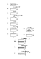
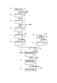
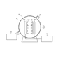
- FIGS. 9A to 9K are schematic cross-sectional views illustrating a method for manufacturing a polycrystalline diamond free-standing substrate 200 using a plasma bonding method according to the second embodiment of the present invention. It is a schematic cross section of the vacuum room temperature bonding apparatus 50 used in one embodiment of the present invention.
- FIG. 1 Manufacturing method of polycrystalline diamond free-standing substrate
- a solution containing diamond particles is applied onto a single crystal silicon substrate 10.
- the diamond particle-containing liquid film 12 is formed on the single crystal silicon substrate 10.
- the single crystal silicon substrate 10 is heat-treated to evaporate the solvent in the diamond particle-containing liquid film 12, and to remove the solvent from the surface of the single crystal silicon substrate 10.
- the bonding force with the diamond particles 14 is strengthened, and the diamond particles 14 are attached to the single crystal silicon substrate 10.
- a thickness of 100 ⁇ m or more is formed on the single crystal silicon substrate 10 by a chemical vapor deposition method (CVD method) with the diamond particles 14 as nuclei. Of polycrystalline diamond layer 16 is grown. Thereafter, as shown in FIGS. 1D and 1E, the surface 16A of the polycrystalline diamond layer is flattened.
- CVD method chemical vapor deposition method
- an ion beam or neutral is applied to the surface 16A of the polycrystalline diamond layer and the surface 20A of the compound semiconductor substrate 20 at room temperature in vacuum.
- Atom beam is irradiated to make both surfaces 16A and 20A active surfaces.
- a region 18 in the surface layer portion of the polycrystalline diamond layer 16, a region 18 (hereinafter referred to as “sp 2 region”) in which a part of diamond (sp 3 ) particles is sp 2 is formed. Referred to as) is formed.
- an amorphous layer 22 of a compound semiconductor is formed on the surface layer portion of the compound semiconductor substrate 20.
- the two activation surfaces are continuously brought into contact with each other at room temperature in vacuum, so that the activation surfaces serve as bonding surfaces (bonding surfaces).
- the polycrystalline diamond layer 16 and the compound semiconductor substrate 20 are bonded together to obtain a bonded substrate 30.
- the compound semiconductor substrate 20 is reduced in thickness to form a compound semiconductor layer 26.
- the single crystal silicon substrate 10 is removed from the bonded substrate 30.
- the polycrystalline diamond free-standing substrate 100 in which the polycrystalline diamond layer 16 functions as a supporting substrate for the compound semiconductor layer 26 can be manufactured through the above steps.
- the compound semiconductor layer 26 becomes a device layer for forming a semiconductor device.
- an amorphous layer of diamond (sp 2 region) 18 and an amorphous layer of compound semiconductor 22 exist between the surface of the polycrystalline diamond layer 16 and the compound semiconductor layer 26.
- FIGS. 2A to 2E A method for manufacturing a polycrystalline diamond free-standing substrate 200 using a plasma bonding method according to a second embodiment of the present invention will be described with reference to FIG. Since the steps of FIGS. 2A to 2E are the same as the steps of FIGS. 1A to 1E, description thereof will be omitted.
- an oxide film 24A that functions as an adhesion layer is formed on the surface 16A of the polycrystalline diamond layer and the surface 20A of the compound semiconductor substrate 20, respectively.
- an oxide film 24B is formed.
- the compound semiconductor substrate 20 is bonded to the polycrystalline diamond layer 16 by a plasma bonding method to obtain a bonded substrate 40.
- the surface of the oxide film 24A and the oxide film 24B is subjected to plasma treatment in an atmosphere composed of at least one of oxygen, nitrogen, hydrogen, and argon, and then the polycrystalline diamond is interposed through the oxide films 24A and 24B.
- the polycrystalline diamond layer 16 and the compound semiconductor substrate 20 are bonded to each other by superposing the layer 16 and the compound semiconductor substrate 20 on each other and performing heat treatment. Thereafter, as shown in FIGS. 2I and 2J, the compound semiconductor substrate 20 is thinned to form the compound semiconductor layer 26. Thereafter, as shown in FIGS. 1J and 1K, the single crystal silicon substrate 10 is removed from the bonded substrate 40.
- the polycrystalline diamond free-standing substrate 200 in which the polycrystalline diamond layer 16 functions as a supporting substrate for the compound semiconductor layer 26 can be manufactured through the above steps.
- the compound semiconductor layer 26 becomes a device layer for forming a semiconductor device.
- an oxide film 24 exists between the surface of the polycrystalline diamond layer 16 and the compound semiconductor layer 26.
- the polycrystalline diamond layer 16 having the maximum grain size of the crystal grains on the surface 16A of the polycrystalline diamond layer is formed. It is essential that the value divided by the thickness be 0.20 or less, and the technical significance thereof will be described later. Hereinafter, each step in the first and second embodiments will be described in detail.
- the attaching step of attaching the diamond particles 14 onto the single crystal silicon substrate 10 may be performed by applying a solution containing the diamond particles onto the single crystal silicon substrate 10 and then subjecting the single crystal silicon substrate 10 to heat treatment. preferable.
- a solution containing diamond particles is applied onto a single crystal silicon substrate 10 to form a diamond on the single crystal silicon substrate 10.
- the particle-containing liquid film 12 is formed.
- the coating method include a spin coating method, a spraying method, and a dipping method, and the spin coating method is particularly preferable. According to the spin coating method, the diamond particle-containing solution can be uniformly applied to only one surface of both surfaces of the single crystal silicon substrate 10 to which the diamond particles 14 are to be attached.
- the average particle diameter of diamond particles contained in the diamond particle-containing solution is preferably 1 nm or more and 50 nm or less, and more preferably 10 nm or less. If it is 1 nm or more, it is possible to suppress the phenomenon that the diamond particles 14 are flipped from the surface of the single crystal silicon substrate 10 by the sputtering action in the initial stage of growing the polycrystalline diamond layer 16, and if it is 50 nm or less, Even if the polycrystalline diamond layer 16 is formed to a thickness of 100 ⁇ m or more, the polycrystalline diamond can be densely grown without abnormal growth, and the maximum grain size of crystal grains on the surface 16A is divided by the thickness of the polycrystalline diamond layer. This is because the value can be set to 0.20 or less.
- Diamond particles of such a size can be suitably prepared from graphite by a known detonation method, implosion method or pulverization method.
- the “average particle size of diamond particles contained in the solution containing diamond particles” is calculated according to JIS 8819-2, and the particle size distribution measured by a known laser diffraction type particle size distribution measuring device follows a normal distribution. Means the average particle size calculated on the assumption.
- the single crystal silicon substrate 10 before being coated with the diamond particle-containing solution is generally acid-washed with hydrofluoric acid or the like in order to remove metal impurities attached to the surface thereof. Since the surface of the acid-cleaned single crystal silicon substrate 10 is an active water-repellent surface, particles easily adhere to the surface. Therefore, it is preferable to wash the acid-cleaned single crystal silicon substrate 10 with pure water or the like to make the surface of the single crystal silicon substrate 10 a hydrophilic surface on which a natural oxide film is formed. Alternatively, it is preferable to leave the acid-cleaned single crystal silicon substrate 10 in a clean room for a long time to form a natural oxide film on the surface of the single crystal silicon substrate 10.
- oxidation treatment a method of heating the diamond particles for oxidation, a method of immersing the diamond particles in an ozone solution, a nitric acid solution, an aqueous hydrogen peroxide solution, or a perchloric acid solution can be mentioned.
- Examples of the solvent for the diamond particle-containing solution include water, as well as organic solvents such as methanol, ethanol, 2-propanol, and toluene. These solvents may be used alone or in combination of two or more. May be.
- the content of diamond particles in the diamond particle-containing solution is preferably 0.03% by mass or more and 10% by mass or less based on the entire diamond particle-containing solution.
- the content is 0.03 mass% or more, the diamond particles 14 can be uniformly adhered to the single crystal silicon substrate 10, and when the content is 10 mass% or less, the adhered diamond particles 14 are generated in the growth process of the diamond layer 16. This is because abnormal growth can be suppressed.
- the diamond particle-containing solution is preferably in the form of gel, and the diamond particle-containing solution may contain a thickening agent.
- the thickener include agar, carrageenan, xanthan gum, gellan gum, guar gum, polyvinyl alcohol, polyacrylate thickeners, water-soluble celluloses, polyethylene oxide, etc., and one or more of them should be used. You can When a thickening agent is contained, it is preferable that the pH of the diamond particle-containing solution is in the range of 6 or more and 8 or less.
- the diamond particle-containing solution may be prepared by mixing diamond particles with the above solvent and stirring the solution to disperse the diamond particles in the solvent.
- the stirring speed is preferably 500 rpm or more and 3000 rpm or less, and the stirring time is preferably 10 minutes or more and 1 hour or less.
- the single crystal silicon substrate 10 is heat-treated.
- the solvent in the diamond particle-containing liquid film 12 evaporates, the bonding force between the surface of the single crystal silicon substrate 10 and the diamond particles 14 is strengthened, and the diamond particles 14 adhere to the single crystal silicon substrate 10. .
- the temperature of the single crystal silicon substrate 10 during the heat treatment is preferably less than 100°C, more preferably 30°C or more and 80°C or less.
- the temperature is lower than 100° C., it is possible to suppress the generation of bubbles accompanying the boiling of the diamond particle-containing solution, so that there is no occurrence of a site on the single crystal silicon substrate 10 where the diamond particles 14 are partially absent. There is no possibility that the polycrystalline diamond layer 16 will peel off from this portion as a starting point. If the temperature is 30° C. or higher, the single crystal silicon substrate 10 and the diamond particles 14 are sufficiently bonded to each other. Therefore, in the process of growing the polycrystalline diamond layer 16 by the CVD method, the diamond particles 14 are prevented from being repelled by the sputtering action. It can be suppressed and the polycrystalline diamond layer 16 can be grown uniformly.
- the heat treatment time is preferably 1 minute or more and 30 minutes or less.
- a known heat treatment apparatus may be used as the heat treatment apparatus, and for example, the single crystal silicon substrate 10 may be placed on a heated hot plate.
- the method of depositing diamond particles on the single crystal silicon substrate is not limited to the coating method of coating a solution containing diamond particles, and may be a known scratching method.
- the scratching method diamond particles are embedded on the surface of the single crystal silicon substrate to adhere the diamond particles to the single crystal silicon substrate.
- a method for embedding diamond particles (1) a method in which dry diamond powder is distributed on the surface of a single crystal silicon substrate and a pressing force is applied to the substrate surface, (2) a high-speed gas containing diamond particles A method of spraying on the surface of a crystalline silicon substrate, (3) a method of placing a single crystalline silicon substrate in a fluidized bed of diamond particles, and (4) a method of ultrasonically cleaning a single crystalline silicon substrate in a solution in which diamond particles are dispersed. And so on.
- the scratching method the depth of embedding of the diamond particles varies, resulting in an uneven thickness of the polycrystalline diamond layer or scratches on the surface of the single crystal silicon substrate when embedding the diamond particles. If it is large, the smoothness of the surface of the polycrystalline diamond layer tends to deteriorate, so that it is preferable to use the coating method.
- a thickness of 100 ⁇ m or more is formed on the single crystal silicon substrate 10 by a CVD method using the diamond particles 14 as nuclei. Of polycrystalline diamond layer 16 is grown. At this time, it is important to set the value obtained by dividing the maximum grain size of the crystal grains on the surface 16A of the polycrystalline diamond layer by the thickness of the polycrystalline diamond layer 16 to 0.20 or less.
- a plasma CVD method, a hot filament CVD method, or the like can be preferably used.
- the “maximum grain size of crystal grains on the surface of the polycrystalline diamond layer” and the “thickness of the polycrystalline diamond layer” are defined as follows. That is, the center point of the surface 16A of the polycrystalline diamond layer (that is, the center point of the wafer), the circumference with a radius of 95% of the surface 16A of the polycrystalline diamond layer, and the diameter of the surface 16A of the polycrystalline diamond layer Three areas of 10 ⁇ m ⁇ 10 ⁇ m centered on a total of three intersections are observed in a plane with an optical microscope. Here, the center of the circumference coincides with the center point of the surface 16A of the polycrystalline diamond layer.
- the largest one of the major axes of all the crystal grains in these three regions is defined as the “maximum grain size of the crystal grains”.
- the average value of the thicknesses measured by observing the cross-sections of the above three regions with an optical microscope is adopted.
- the microwave plasma CVD method is a method in which a source gas such as methane is decomposed by microwaves in a plasma chamber into plasma, and the source gas converted into plasma is introduced onto a heated single crystal silicon substrate 10 to form a polycrystalline diamond layer. This is a method of growing 16.
- the pressure in the plasma chamber, the microwave output, and the temperature of the single crystal silicon substrate 10 are preferably set as follows.
- the pressure in the plasma chamber is preferably 1.3 ⁇ 10 3 Pa or more and 1.3 ⁇ 10 5 Pa or less, more preferably 1.1 ⁇ 10 4 Pa or more and 4.0 ⁇ 10 4 Pa or less. preferable.
- the microwave output is preferably 0.1 kW or more and 100 kW or less, and more preferably 1 kW or more and 10 kW or less.
- the temperature of the single crystal silicon substrate 10 is preferably 700° C. or higher and 1300° C. or lower, and more preferably 900° C. or higher and 1200° C. or lower.
- the hot filament CVD method When the hot filament CVD method is used, a filament made of tungsten, tantalum, rhenium, molybdenum, iridium or the like is used, the filament temperature is set to about 1900° C. or higher and 2300° C. or lower, and carbon radicals are generated from a hydrocarbon-based source gas such as methane. To generate. By introducing this carbon radical onto the heated single crystal silicon substrate 10, the polycrystalline diamond layer 16 is grown. According to the hot filament CVD method, it is possible to easily cope with an increase in the diameter of the wafer.
- the pressure in the chamber, the distance between the filament and the single crystal silicon substrate 10, and the temperature of the single crystal silicon substrate 10 are preferably set as follows.
- the pressure in the chamber is preferably 1.3 ⁇ 10 3 Pa or more and 1.3 ⁇ 10 5 Pa or less.
- the distance between the filament and the single crystal silicon substrate 10 is preferably 5 mm or more and 20 mm or less.
- the temperature of the single crystal silicon substrate 10 is preferably 700° C. or higher and 1300° C. or lower.
- the polycrystalline diamond layer 16 functions as a support substrate for the compound semiconductor layer 26, its thickness is 100 ⁇ m or more, and more preferably 500 ⁇ m or more.
- the upper limit of the thickness of the polycrystalline diamond layer 16 is not particularly limited, but it is preferably 3 mm or less from the viewpoint that the process time during growth by the CVD method is not excessive.
- the surface 16A of the polycrystalline diamond layer is flattened.
- the planarization method is not particularly limited, but for example, a known chemical mechanical polishing (CMP) method can be preferably used. Even after the flattening, the thickness of the polycrystalline diamond layer 16 is 100 ⁇ m or more, more preferably 500 ⁇ m or more.
- the polycrystalline diamond layer 16 having the surface 16A in which the value obtained by dividing the maximum grain size of the crystal grains by the thickness of the polycrystalline diamond layer is 0.20 or less is used. It is important to use the flattening process.
- the crystallinity of the diamond layer formed on the single crystal silicon substrate 10 by the CVD method is polycrystalline.
- the grain size of the diamond crystal grains is large, the crystal grains cannot exist densely on the surface of the polycrystalline diamond layer, and the depth position is different between a certain crystal grain and the crystal grains existing around it.
- a gap is formed around the crystal grains. Therefore, even if the surface of a certain crystal grain is polished, the crystal grain existing at a deeper position is exposed on the surface in an unpolished state.
- the surface roughness Ra of the polycrystalline diamond layer does not become small even if the surface is polished.
- the surface 16A of the polycrystalline diamond layer is polished. In doing so, the surface roughness Ra can be adjusted to 3 nm or less. If Ra of the surface 16A of the polycrystalline diamond layer after planarization is 3 nm or less, the polycrystalline diamond layer 16 and the compound semiconductor substrate 20 are bonded and bonded together by a vacuum room temperature bonding method or a plasma bonding method described later. it can.
- the surface roughness Ra in this specification means the arithmetic mean roughness Ra specified in JIS B 0601 (2001).
- the compound semiconductor substrate 20 is bonded to the polycrystalline diamond layer 16 by a vacuum room temperature bonding method,
- the bonded substrate stack 30 is obtained.
- the vacuum room temperature bonding method is a method of bonding the single crystal silicon substrate 10 and the compound semiconductor substrate 20 at room temperature without heating.
- the surface 16A of the polycrystalline diamond layer and the surface 20A of the compound semiconductor substrate are activated by irradiation with an ion beam or a neutral atom beam under vacuum room temperature to activate both surfaces 16A and 20A. Face. As a result, dangling bonds appear on the activated surface.
- the bonding force is instantaneously exerted, and the polycrystalline diamond layer 16 and the compound semiconductor substrate 20 are firmly adhered to each other using the activation surface as a bonding surface. Fit.
- the vacuum room temperature bonding apparatus 50 includes a plasma chamber 51, a gas introduction port 52, a vacuum pump 53, a pulse voltage application device 54, and wafer fixing bases 55A and 55B.
- the single crystal silicon substrate 10 and the compound semiconductor substrate 20 are placed and fixed on the wafer fixing bases 55A and 55B in the plasma chamber 51, respectively.
- the inside of the plasma chamber 51 is decompressed by the vacuum pump 53, and then the source gas is introduced into the plasma chamber 51 from the gas inlet 52.
- the pulse voltage applying device 54 applies a negative voltage in a pulse shape to the wafer fixing bases 55A and 55B (and the single crystal silicon substrate 10 and the compound semiconductor substrate 20).
- plasma of the source gas is generated, and ions of the source gas contained in the generated plasma are accelerated toward the surfaces of the polycrystalline diamond layer 16 and the compound semiconductor substrate 20 formed on the single crystal silicon substrate 10, Can be irradiated.
- the irradiation element is preferably at least one selected from Ar, Ne, Xe, H, He and Si.
- the chamber pressure in the plasma chamber 51 is preferably 1 ⁇ 10 ⁇ 5 Pa or less. If it is 1 ⁇ 10 ⁇ 5 Pa or less, it is difficult for the sputtered element to re-attach to the surface of each substrate, and there is no fear that the dangling bond formation rate will decrease.
- the pulse voltage applied to the single crystal silicon substrate 10 and the compound semiconductor substrate 20 is preferably set so that the acceleration energy of the irradiation element with respect to the surface of each substrate is 100 eV or more and 10 keV or less. If it is 100 eV or more, the irradiated element is not likely to be deposited on the surface of each substrate, and if it is 10 keV or less, the irradiated element is not likely to be injected into each substrate, so that the dangling bond is stable. This is because it can be formed.
- the frequency of the pulse voltage determines the number of times the single crystal silicon substrate 10 and the compound semiconductor substrate 20 are irradiated with ions or neutral atoms.
- the frequency of the pulse voltage is preferably 10 Hz or more and 10 kHz or less. If it is 10 Hz or more, the irradiation variation of ions or neutral atoms can be absorbed, so that the irradiation dose of ions or neutral atoms is stable, and if it is 10 kHz or less, plasma formation by glow discharge is stable. is there.
- the pulse width of the pulse voltage determines the time for which the single crystal silicon substrate 10 and the compound semiconductor substrate 20 are irradiated with ions or neutral atoms.
- the pulse width is preferably 1 ⁇ sec or more and 10 msec or less. If it is 1 ⁇ sec or more, each substrate can be stably irradiated with ions or neutral atoms, and if it is 10 msec or less, plasma formation by glow discharge is stable.
- the temperature thereof is normal temperature (usually 30°C to 90°C).
- the vacuum room temperature bonding method By using the vacuum room temperature bonding method in this way, the following effects can be obtained.
- the single crystal silicon substrate 10 and the compound semiconductor substrate 20 are not heated. Therefore, it is possible to suppress the impurities in the single crystal silicon substrate 10 from diffusing outward into the compound semiconductor substrate 20.
- the two substrates can be joined instantaneously and firmly, the occurrence of slip and dislocation can be prevented.
- thermal stress due to high temperature heat treatment is not introduced into the polycrystalline diamond layer 16.
- the amorphous layer 22 having a thickness of 1 nm or more and 5 nm or less is formed on the surface layer portion of the compound semiconductor substrate 20 (FIG. 1(I)).
- the amorphous layer 22 functions as a gettering layer and can suppress outward diffusion of oxygen and impurities in the single crystal silicon substrate 10 to the compound semiconductor substrate 20. Further, since the amorphous layer 22 has good thermal conductivity, it contributes to the improvement of heat dissipation of the final polycrystalline diamond freestanding substrate 100.
- the plasma bonding method is a wafer bonding method in which dangling bonds are formed on each surface by exposing the surface of the polycrystalline diamond layer and the surface of the compound semiconductor substrate to a plasma atmosphere, and the dangling bonds are bonded to each other.
- the plasma activation process and the wafer bonding process are performed by different devices, so the activated dangling bonds are once exposed to the air, the dangling bond density decreases, and the wafer bonding strength decreases. .. Therefore, in order to secure the wafer bonding strength, heat treatment is required after the wafer bonding.
- an oxide film 24A and an oxide film 24B functioning as adhesion layers are formed on the surface 16A of the polycrystalline diamond layer and the surface 20A of the compound semiconductor substrate 20, respectively.
- both the oxide film 24A and the oxide film 24B are formed, but in the present invention, at least one of them may be formed.
- the oxide film 24A is preferably formed by the following method. That is, since the polycrystalline diamond is gasified into CO 2 by the thermal oxidation method, it is difficult to form an oxide film by thermal oxidation. Therefore, a silicon oxide film 24A having a thickness of 100 nm or more and 1 ⁇ m or less, preferably 100 nm or more and 500 nm or less is formed on the surface of the polycrystalline diamond layer by a deposition method (for example, a CVD method or a sputtering method).
- a deposition method for example, a CVD method or a sputtering method.
- the oxide film 24B can be formed by either a thermal oxidation method or a deposition method. That is, the silicon oxide film 24B having a thickness of 100 nm or more and 1 ⁇ m or less, preferably 100 nm or more and 500 nm or less may be formed on the surface of the compound semiconductor substrate by a deposition method (for example, a CVD method or a sputtering method). Alternatively, the compound semiconductor substrate may be thermally oxidized to form an oxide film 24B having a thickness of 100 nm or more and 1 ⁇ m or less, preferably 100 nm or more and 500 nm or less on the surface layer portion thereof.
- a deposition method for example, a CVD method or a sputtering method.
- the compound semiconductor substrate may be thermally oxidized to form an oxide film 24B having a thickness of 100 nm or more and 1 ⁇ m or less, preferably 100 nm or more and 500 nm or less on the surface layer portion thereof.
- the surface of the oxide film 24A and the surface of the oxide film 24B are subjected to plasma treatment in an atmosphere containing at least one of oxygen, nitrogen, hydrogen, and argon.
- the oxide film 24A or the oxide film 24B is not formed, the surface 16A of the polycrystalline diamond layer or the surface 20A of the compound semiconductor substrate is plasma-treated, respectively.
- a plasma atmosphere it is preferable to apply 50 W or more and 200 W or less in the plasma chamber. If it is 50 W or more, a plasma atmosphere can be stably formed, and if it is 200 W or less, plasma can be uniformly formed.
- the chamber pressure in the plasma chamber is preferably set in the range of 10 Pa or more and 100 Pa or less. This is because if the pressure is 100 Pa or less, the sputtered element is unlikely to redeposit on the surface of each substrate and the dangling bond formation rate does not decrease.
- the frequency of the applied pulse voltage for plasma formation is preferably 0.5 MHz or more and 2 MHz or less. This is because if it is 0.5 MHz or more, plasma can be stably formed, and if it is 2 MHz or less, dangling bonds can be stably formed on the surface to be plasma-treated.
- the plasma conditions for the single crystal silicon substrate 10 and the compound semiconductor substrate 20 are preferably set so that the acceleration energy of the irradiation elements (oxygen, nitrogen, hydrogen and argon) with respect to the surface of each substrate is 100 eV or more and 10 keV or less. If it is 100 eV or more, the irradiated element is not likely to be deposited on the surface of each substrate, and if it is 10 keV or less, the irradiated element is not likely to be injected into each substrate, so that the dangling bond is stable. This is because it can be formed.
- the acceleration energy of the irradiation elements oxygen, nitrogen, hydrogen and argon
- the polycrystalline diamond layer 16 and the compound semiconductor substrate 20 are superposed on each other through the oxide films 24A and 24B and heat-treated to bond the polycrystalline diamond layer 16 and the compound semiconductor substrate 20 to each other.
- the heat treatment is preferably performed under an atmosphere of at least one of oxygen, nitrogen, hydrogen, and argon at an ambient temperature of 300° C. to 1000° C. for 10 minutes to 2 hours. It may be considered that the substrate temperature is equal to the ambient temperature of the heat treatment chamber.
- the plasma bonding method By using the plasma bonding method in this way, the following effects can be obtained.
- the plasma bonding method since the polycrystalline diamond layer 16 and the compound semiconductor substrate 20 are bonded via the oxide film, impurities diffusing from the polycrystalline diamond layer to the compound semiconductor substrate can be trapped in the oxide film. It is possible to suppress the diffusion of impurities into the compound semiconductor substrate.
- the compound semiconductor substrate 20 is thinned to form the compound semiconductor layer 26.
- the compound semiconductor substrate 20 is thinned by grinding and polishing from the surface opposite to the bonding surface.
- the thickness of the compound semiconductor layer 26 can be appropriately determined according to the type and structure of the semiconductor device formed therein, and is preferably 1 ⁇ m or more and 500 ⁇ m or less.
- a known or arbitrary grinding method and polishing method can be preferably used, and specifically, a surface grinding method and a mirror polishing method can be used.
- the single crystal silicon substrate 10 is removed from the bonded substrates 30 and 40.
- the polycrystalline diamond free-standing substrates 100 and 200 in which the compound semiconductor layer 26 having a desired thickness is laminated on the polycrystalline diamond layer 16 as the supporting substrate can be obtained.
- the removing method is not particularly limited, and, for example, a known or arbitrary grinding method and polishing method can be preferably used, and specifically, a surface grinding method and a mirror polishing method can be used. Alternatively, a chemical etching method such as wet etching or dry etching can be used.
- the single crystal silicon substrate 10 is a wire saw made of a single crystal silicon ingot grown by the MCZ method (Magnetic field applied Czochralski method) or the floating zone melting method (FZ method) in which a magnetic field is applied to the Czochralski method (CZ method) or the CZ method. You can use the sliced one.
- MCZ method Magnetic field applied Czochralski method
- FZ method floating zone melting method
- the oxygen concentration of the single crystal silicon substrate 10 is preferably 5 ⁇ 10 17 atoms/cm 3 or less.
- the “oxygen concentration” in the present specification means the average value of the oxygen concentration in the thickness direction of the substrate as measured by the FT-IR method (Old ASTM F121-1979). According to the study by the present inventors, it has been found that there is a correlation between the oxygen concentration of the single crystal silicon substrate 10 and the maximum grain size of the crystal grains on the surface 16A of the polycrystalline diamond layer.
- the low oxygen concentration single crystal silicon substrate 10 as described above is used, even if the polycrystalline diamond layer 16 is formed to a thickness of 100 ⁇ m or more without special measures at the time of film formation by the CVD method, It was found that the value obtained by dividing the maximum grain size of the crystal grains on the surface 16A by the thickness of the polycrystalline diamond layer 16 can be controlled to 0.20 or less.
- the thickness of the single crystal silicon substrate 10 may be set according to the thickness of the polycrystalline diamond layer 16, and the thicker the polycrystalline diamond layer 16 is, the larger the warp is. Therefore, the single crystal silicon substrate 10 is prevented from causing the warp. It is preferable to make 10 thick. Specifically, the thickness of the single crystal silicon substrate 10 is preferably 1 mm or more and 5 mm or less.
- the compound semiconductor forming the compound semiconductor substrate 20 is not particularly limited, and may be appropriately selected according to the type of semiconductor device formed in the compound semiconductor layer 26, for example, GaN, AlN, InN, SiC, Al 2 O. It is preferably made of 3 , Ga 2 O 3 , MgO, ZnO, CdO, GaAs, GaP, GaSb, InP, InAs, InSb, or SiGe.
- the thickness of the compound semiconductor substrate 20 is preferably 200 ⁇ m or more and 3 mm or less. When the thickness is less than 200 ⁇ m, the compound semiconductor substrate warps to cause peeling of polycrystalline diamond or cracking of the compound semiconductor substrate. Further, when it exceeds 3 mm, it is not preferable from the viewpoint of process time and material cost in the step of reducing the thickness of the compound semiconductor substrate 20 described later.
- a polycrystalline diamond free-standing substrate 100 manufactured according to the first embodiment of the present invention includes a support substrate formed of a polycrystalline diamond layer 16 having a thickness of 100 ⁇ m or more, and a polycrystalline diamond.
- 18 and an amorphous layer 22 of the compound semiconductor that constitutes the compound semiconductor layer The thickness of each layer 18, 22 is 1 nm or more and 5 nm or less.
- a polycrystalline diamond free-standing substrate 200 manufactured according to the second embodiment of the present invention includes a support substrate including a polycrystalline diamond layer 16 having a thickness of 100 ⁇ m or more, A compound semiconductor layer 26 formed on the surface of the crystalline diamond layer 16, and a silicon oxide film having a total thickness of 200 nm or more and 2 ⁇ m or less between the surface of the polycrystalline diamond layer 16 and the compound semiconductor layer 26. At least one of the oxide film of the compound semiconductor forming the film and the compound semiconductor layer (the oxide film 24) exists.
- Each of the polycrystalline diamond free-standing substrates 100 and 200 is characterized in that the maximum grain size of crystal grains on the surface of the polycrystalline diamond layer divided by the thickness of the polycrystalline diamond layer is 0.20 or less. Since the polycrystalline diamond free-standing substrates 100 and 200 are formed by stacking high-quality compound semiconductor layers 26 and have the polycrystalline diamond layer 16 having high thermal conductivity, the heat dissipation is high. Further, in the polycrystalline diamond free-standing substrate 100, the amorphous layer 22 also has high thermal conductivity, so that higher heat dissipation can be obtained.
- the compound semiconductor layer 26 is made of GaN, AlN, InN, SiC, Al 2 O 3 , Ga 2 O 3 , MgO, ZnO, CdO, GaAs, GaP, GaSb, InP, InAs, InSb, or SiGe. Is preferable, and its thickness is preferably 1 ⁇ m or more and 500 ⁇ m or less as described above.
- Example 1 Vacuum room temperature bonding method
- a single crystal silicon substrate having a diameter of 2 inches, a thickness of 3 mm, a resistivity of 10 ⁇ cm, and an oxygen concentration shown in Table 1 was prepared by cutting out a single crystal silicon ingot grown by the CZ method.
- a GaN substrate having a diameter of 2 inches and a thickness of 600 ⁇ m was prepared by cutting out a gallium nitride (GaN) single crystal produced by the HVPE (Hydride Vapor Phase Epitaxy) method.
- diamond particles having an average particle size of 6 nm were prepared by the detonation method.
- the diamond particles were immersed in an aqueous solution of hydrogen peroxide, terminated with a carboxyl group (COOH), and charged with a negative charge.
- the diamond particles were mixed with a solvent (H 2 O) and stirred to prepare a diamond particle-containing solution having a diamond particle content of 6 mass %.
- the stirring speed was 1100 rpm, the stirring time was 50 minutes, and the temperature of the diamond particle-containing solution during stirring was 25°C.
- the single crystal silicon substrate is washed with pure water to form a natural oxide film on the surface, and then a diamond particle-containing solution is applied on the single crystal silicon substrate by spin coating to form a diamond particle-containing liquid film. did.
- the single crystal silicon substrate is placed on a hot plate set at 80° C. for 5 minutes to perform heat treatment for strengthening the bond between the single crystal silicon substrate and the diamond particles, and the diamond particles are attached to the single crystal silicon substrate.
- a polycrystalline diamond layer having a thickness of 300 ⁇ m is grown using the diamond particles attached to the single crystal silicon substrate as nuclei.
- the pressure in the plasma chamber was 1.5 ⁇ 10 4 Pa
- the microwave output was 5 kW
- the temperature of the single crystal silicon substrate was 1050° C.
- the maximum grain size of crystal grains on the surface of the polycrystalline diamond layer was measured by the method described above. The results are shown in Table 1.
- the surface of the polycrystalline diamond layer was flattened by the CMP method.
- the thickness of the polycrystalline diamond layer after flattening was 290 ⁇ m.
- the surface roughness Ra of the surface of the polycrystalline diamond layer was measured by the method described above. The measurement results are shown in Table 1.
- Ar is caused to flow in a vacuum chamber at 25° C. and 1 ⁇ 10 ⁇ 5 Pa to generate plasma, and acceleration energy: 1.0 keV, frequency: 140 Hz, on the surface of the polycrystalline diamond layer and the surface of the GaN substrate.
- Irradiation with Ar ions was performed with a pulse width of 55 ⁇ sec to make both the above surfaces active surfaces.
- an attempt was made to bond the polycrystalline diamond layer and the GaN substrate with the activation surface as the bonding surface.
- Table 1 shows the possibility of joining at this time.
- an amorphous layer having a thickness of 1 nm was formed on the surface of the polycrystalline diamond layer, and an amorphous layer having a thickness of 1 nm was formed on the surface layer of the GaN substrate.
- the GaN substrate was ground and polished to form a GaN layer having a thickness of 10 ⁇ m. Further, the single crystal silicon substrate was removed by grinding and polishing. In this way, a free standing polycrystalline diamond substrate was obtained in which a 10 ⁇ m thick GaN layer was laminated on a 290 ⁇ m thick polycrystalline diamond layer. When the cross section of the GaN layer was observed by TEM, no dislocation was observed as shown in Table 1.
- Example 2 Plasma bonding method
- a single crystal silicon substrate having a diameter of 2 inches, a thickness of 3 mm, a resistivity of 10 ⁇ cm, and an oxygen concentration shown in Table 2 was prepared by cutting from a single crystal silicon ingot grown by the CZ method.
- a GaN substrate having a diameter of 2 inches and a thickness of 600 ⁇ m was prepared by cutting out a gallium nitride (GaN) single crystal produced by the HVPE (Hydride Vapor Phase Epitaxy) method.
- diamond particles having an average particle size of 6 nm were prepared by the detonation method.
- the diamond particles were immersed in an aqueous solution of hydrogen peroxide, terminated with a carboxyl group (COOH), and charged with a negative charge.
- the diamond particles were mixed with a solvent (H 2 O) and stirred to prepare a diamond particle-containing solution having a diamond particle content of 3% by mass.
- the stirring speed was 1100 rpm, the stirring time was 50 minutes, and the temperature of the diamond particle-containing solution during stirring was 25°C.
- the single crystal silicon substrate is washed with pure water to form a natural oxide film on the surface, and then a diamond particle-containing solution is applied on the single crystal silicon substrate by spin coating to form a diamond particle-containing liquid film. did.
- the single crystal silicon substrate is placed on a hot plate set at 80° C. for 5 minutes to perform heat treatment for strengthening the bond between the single crystal silicon substrate and the diamond particles, and the diamond particles are attached to the single crystal silicon substrate.
- a polycrystalline diamond layer having a thickness of 300 ⁇ m is grown using the diamond particles attached to the single crystal silicon substrate as nuclei.
- the pressure in the plasma chamber was 1.5 ⁇ 10 4 Pa
- the microwave output was 5 kW
- the temperature of the single crystal silicon substrate was 1050° C.
- the maximum grain size of crystal grains on the surface of the polycrystalline diamond layer was measured by the method described above. The results are shown in Table 2.
- the surface of the polycrystalline diamond layer was flattened by the CMP method.
- the thickness of the polycrystalline diamond layer after flattening was 290 ⁇ m.
- the surface roughness Ra of the surface of the polycrystalline diamond layer was measured by the method described above. The measurement results are shown in Table 2.
- a 100 nm-thick silicon oxide film was formed on each of the surface of the polycrystalline diamond layer and the surface of the GaN substrate by the CVD method. After that, 100 W was applied at 1 MHz in an oxygen atmosphere having a pressure of 40 Pa in the chamber, and the surfaces of both silicon oxide films were plasma-treated at an acceleration energy of 300 eV. After that, the polycrystalline diamond layer and the GaN layer are overlapped with each other through the silicon oxide film, and heat treatment is performed at 500° C. for 1 hour in a nitrogen atmosphere to try to bond the polycrystalline diamond layer and the GaN substrate. It was Table 2 shows the possibility of joining at this time.
- the GaN substrate was ground and polished to form a GaN layer having a thickness of 10 ⁇ m. Further, the single crystal silicon substrate was removed by grinding and polishing. In this way, a free standing polycrystalline diamond substrate was obtained in which a 10 ⁇ m thick GaN layer was laminated on a 290 ⁇ m thick polycrystalline diamond layer. When the cross section of the GaN layer was observed by TEM, no dislocation was observed as shown in Table 2.
- Example 3 Plasma bonding method
- the GaN substrate was ground and polished to form a GaN layer having a thickness of 10 ⁇ m. Further, the single crystal silicon substrate was removed by grinding and polishing. In this way, a free standing polycrystalline diamond substrate was obtained in which a 10 ⁇ m thick GaN layer was laminated on a 290 ⁇ m thick polycrystalline diamond layer. When the cross section of the GaN layer was observed by TEM, dislocations were not observed as shown in Table 3.
- Example 4 A single crystal silicon substrate having a diameter of 2 inches, a thickness of 3 mm, a resistivity of 10 ⁇ cm, and an oxygen concentration of 3.0 ⁇ 10 17 atoms/cm 3 was prepared.
- a GaN layer having a thickness of 10 ⁇ m was formed on a single crystal silicon substrate by flowing a trimethylgallium gas and an ammonia gas by MOCVD at 1100° C.
- diamond particles were embedded in the surface of the GaN layer by a known scratching method. That is, the single crystal silicon substrate was ultrasonically cleaned in a solution containing diamond particles having an average particle size of 1 ⁇ m to embed the diamond particles on the surface of the GaN layer.
- a 300 ⁇ m-thick polycrystalline diamond layer was grown using the microwave plasma CVD method with the diamond particles embedded on the GaN layer as nuclei.
- the single crystal silicon substrate was removed by grinding and polishing.
- a polycrystalline diamond free-standing substrate in which a 10- ⁇ m-thick GaN layer was laminated on a 300- ⁇ m-thick polycrystalline diamond layer was obtained.
- dislocation was observed when the cross section of the GaN layer was observed by TEM.
- the method for producing a polycrystalline diamond free-standing substrate of the present invention it is possible to produce a polycrystalline diamond free-standing substrate in which high-quality compound semiconductor layers are laminated using a vacuum room temperature bonding method or a plasma bonding method.
Landscapes
- Chemical & Material Sciences (AREA)
- Organic Chemistry (AREA)
- General Chemical & Material Sciences (AREA)
- Chemical Kinetics & Catalysis (AREA)
- Engineering & Computer Science (AREA)
- Materials Engineering (AREA)
- Mechanical Engineering (AREA)
- Metallurgy (AREA)
- Inorganic Chemistry (AREA)
- Life Sciences & Earth Sciences (AREA)
- General Life Sciences & Earth Sciences (AREA)
- Geology (AREA)
- Crystals, And After-Treatments Of Crystals (AREA)
- Recrystallisation Techniques (AREA)
- Carbon And Carbon Compounds (AREA)
- Chemical Vapour Deposition (AREA)
Abstract
高品質な化合物半導体層が積層された多結晶ダイヤモンド自立基板を製造する方法を提供する。単結晶シリコン基板10上に付着させたダイヤモンド粒子14を核として、化学気相成長法により、単結晶シリコン基板10上に厚さが100μm以上の多結晶ダイヤモンド層16を成長させる。その際、多結晶ダイヤモンド層の表面16Aにおける結晶粒の最大粒径を多結晶ダイヤモンド層16の厚さで割った値を0.20以下とする。その後、多結晶ダイヤモンド層の表面16Aを平坦化する。その後、真空常温接合法又はプラズマ接合法により、多結晶ダイヤモンド層16に化合物半導体基板20を貼り合わせる。その後、化合物半導体基板20を減厚して、化合物半導体層22とする。単結晶シリコン基板10を除去する。こうして、多結晶ダイヤモンド層16が化合物半導体層22の支持基板として機能する多結晶ダイヤモンド自立基板100を得る。
Description
本発明は、支持基板としての多結晶ダイヤモンド層上に化合物半導体層が形成されてなる多結晶ダイヤモンド自立基板及びその製造方法に関する。
高周波デバイスやパワーデバイス等の高耐圧の半導体デバイスにおいては、デバイスの自己発熱が問題となる。この対策として、デバイス形成領域の下に熱伝導率が大きい材料を配置する技術が知られている。
例えば、半導体デバイスを形成するためのデバイス層となる窒化ガリウム(GaN)層等の化合物半導体層の直下に、放熱性の高いダイヤモンド層を配置する技術が知られている。特許文献1には、ダイヤモンド上の窒化ガリウム型ウェーハの製造方法が開示されている。この方法は、支持基板上に位置するGaN層上に60nm以下の薄い窒化珪素膜を形成した後に、当該窒化珪素膜の表面に乾式スクラッチによりダイヤモンド粒子を埋め込み固定する工程と、前記表面に固定されたダイヤモンド粒子を核として、化学気相成長法によりGaN層上に前記窒化ケイ素膜を介してダイヤモンド層を成長させる工程と、前記支持基板を除去する工程と、を含み、ダイヤモンド上に窒化ガリウム層が形成されたウェーハを製造するものである。
また、特許文献2には、表面からイオンを注入して内部にイオン注入層を有する窒化物半導体基板を得る工程と、前記窒化物半導体基板の前記イオン注入した表面と、前記窒化物半導体基板と貼り合わせる支持基板の表面との少なくとも一方に表面活性化処理を施す工程と、前記窒化物半導体基板の前記イオン注入した表面と前記支持基板の前記表面とを対向して重ね合わせ、0.5~5.0MPaの圧力下で貼り合わせる工程と、前記窒化物半導体基板を前記イオン注入層に沿って剥離し、前記支持基板上に窒化物半導体薄膜を転写する工程とを少なくとも含む、窒化物半導体薄膜を支持基板に備えた複合基板の製造方法(請求項1)が記載されている。特許文献2では、前記窒化物半導体基板が、GaN基板またはAlN基板であるものとされており(請求項6)、前記支持基板が、シリコン、サファイア、アルミナ、SiC、AlN、SiN及びダイヤモンドからなる群から選択されるものとされている(請求項7)。
本発明者の検討によると、特許文献1に記載の方法では、前記埋め込みに起因してGaN層にクラックが入り、その後の化学気相成長法による高温長時間の熱処理の過程でGaN層内をクラックが進展し、転位が発生することが判明した。このようなGaN層に半導体デバイスを形成すると、リーク電流が増加して、デバイス特性が悪化するおそれがある。
そこで本発明者は、化合物半導体層上にダイヤモンド層を成長させるのではなく、別の基板(すなわち単結晶シリコン基板)上に予め成長させた多結晶ダイヤモンド層に、真空常温接合法又はプラズマ接合法を用いて化合物半導体基板を貼り合わせることを着想した。しかしながら、本発明者の検討によると、単結晶シリコン基板上に成長させた多結晶ダイヤモンド層と化合物半導体基板とを貼り合わせることができないことが判明した。
特許文献2には、シリコン、サファイア、アルミナ、SiC、AlN、SiN及びダイヤモンドからなる群から選択される支持基板と窒化物半導体基板とを接合することが記載されている。しかしながら、実施例において接合できたことが確認されているのは、サファイア基板とGaN基板、及びシリコン基板とGaN基板のみであり、ダイヤモンド基板と窒化物半導体基板との接合は確認されていない。また、特許文献2では、単結晶シリコン基板上に成長させた多結晶ダイヤモンド層と窒化物半導体基板との接合を可能とする条件については、何ら示唆されていない。
上記課題に鑑み、本発明は、真空常温接合法又はプラズマ接合法を用いて高品質な化合物半導体層が積層された多結晶ダイヤモンド自立基板を製造することが可能な、多結晶ダイヤモンド自立基板の製造方法を提供することを目的とする。また、本発明は、高品質な化合物半導体層が積層された多結晶ダイヤモンド自立基板を提供することを目的とする。
上記課題を解決すべく、本発明者は鋭意研究を進め、以下の知見を得た。すなわち、単結晶シリコン基板上に成長させた多結晶ダイヤモンド層と化合物半導体基板との接合の可否は、多結晶ダイヤモンド層の表面における結晶粒の最大粒径と密接に関連しており、単に多結晶ダイヤモンド層の表面を研磨して平坦化しただけでは、貼り合わせることはできないことが分かった。そして、本発明者がさらに検討を進めたところ、多結晶ダイヤモンド層の表面に関して、成膜した多結晶ダイヤモンド層が厚くなるにつれて、多結晶ダイヤモンド層の表面における結晶粒が大きくなり、表面の凹凸も大きくなった。詳細な評価解析の結果、多結晶ダイヤモンド層の表面における結晶粒の最大粒径を多結晶ダイヤモンド層の厚さで割った値が0.20以下になっていれば、多結晶ダイヤモンド層と化合物半導体基板とを貼り合わせ接合できることが分かった。
上記知見に基づき完成した本発明の要旨構成は以下のとおりである。
(1)単結晶シリコン基板上にダイヤモンド粒子を付着させる付着工程と、
前記ダイヤモンド粒子を核として、化学気相成長法により、前記単結晶シリコン基板上に厚さが100μm以上の多結晶ダイヤモンド層を成長させ、その際、該多結晶ダイヤモンド層の表面における結晶粒の最大粒径を前記多結晶ダイヤモンド層の厚さで割った値を0.20以下とする工程と、
前記多結晶ダイヤモンド層の表面を平坦化する平坦化工程と、
その後、真空常温接合法又はプラズマ接合法により、前記多結晶ダイヤモンド層に化合物半導体基板を貼り合わせて、貼り合わせ基板を得る工程と、
その後、前記化合物半導体基板を減厚して、化合物半導体層とする工程と、
前記貼り合わせ基板から前記単結晶シリコン基板を除去して、前記多結晶ダイヤモンド層が、前記化合物半導体層の支持基板として機能する多結晶ダイヤモンド自立基板を得る工程と、
を有することを特徴とする多結晶ダイヤモンド自立基板の製造方法。
(1)単結晶シリコン基板上にダイヤモンド粒子を付着させる付着工程と、
前記ダイヤモンド粒子を核として、化学気相成長法により、前記単結晶シリコン基板上に厚さが100μm以上の多結晶ダイヤモンド層を成長させ、その際、該多結晶ダイヤモンド層の表面における結晶粒の最大粒径を前記多結晶ダイヤモンド層の厚さで割った値を0.20以下とする工程と、
前記多結晶ダイヤモンド層の表面を平坦化する平坦化工程と、
その後、真空常温接合法又はプラズマ接合法により、前記多結晶ダイヤモンド層に化合物半導体基板を貼り合わせて、貼り合わせ基板を得る工程と、
その後、前記化合物半導体基板を減厚して、化合物半導体層とする工程と、
前記貼り合わせ基板から前記単結晶シリコン基板を除去して、前記多結晶ダイヤモンド層が、前記化合物半導体層の支持基板として機能する多結晶ダイヤモンド自立基板を得る工程と、
を有することを特徴とする多結晶ダイヤモンド自立基板の製造方法。
(2)前記真空常温接合法は、
前記多結晶ダイヤモンド層の表面及び前記化合物半導体基板の表面に、真空常温下でイオンビーム又は中性原子ビームを照射して、前記両方の表面を活性化面とする工程と、
引き続き真空常温下で、前記両方の活性化面を接触させることで、前記多結晶ダイヤモンド層と前記化合物半導体基板とを貼り合わせる工程と、
を有する、上記(1)に記載の多結晶ダイヤモンド自立基板の製造方法。
前記多結晶ダイヤモンド層の表面及び前記化合物半導体基板の表面に、真空常温下でイオンビーム又は中性原子ビームを照射して、前記両方の表面を活性化面とする工程と、
引き続き真空常温下で、前記両方の活性化面を接触させることで、前記多結晶ダイヤモンド層と前記化合物半導体基板とを貼り合わせる工程と、
を有する、上記(1)に記載の多結晶ダイヤモンド自立基板の製造方法。
(3)前記プラズマ接合法は、
(i)前記多結晶ダイヤモンド層の表面に厚さ100nm以上1μm以下のシリコン酸化膜を形成すること、及び、(ii)前記化合物半導体基板の表面に厚さ100nm以上1μm以下のシリコン酸化膜を形成する、又は、前記化合物半導体基板を熱酸化して、その表層部に厚さ100nm以上1μm以下の酸化膜を形成すること、の少なくとも一方を行う工程と、
酸素、窒素、水素及びアルゴンの1種類以上からなる雰囲気下で、前記シリコン酸化膜及び前記酸化膜の表面と、前記多結晶ダイヤモンド層の表面及び前記化合物半導体基板の表面のうち前記シリコン酸化膜及び前記酸化膜が形成されていない表面をプラズマ処理する工程と、
前記シリコン酸化膜及び前記酸化膜を介して、前記多結晶ダイヤモンド層と前記化合物半導体基板とを重ね合わせて、雰囲気温度が300℃以上1000℃以下の熱処理を行うことで、前記多結晶ダイヤモンド層と前記化合物半導体基板とを貼り合わせる工程と、
を有する、上記(1)に記載の多結晶ダイヤモンド自立基板の製造方法。
(i)前記多結晶ダイヤモンド層の表面に厚さ100nm以上1μm以下のシリコン酸化膜を形成すること、及び、(ii)前記化合物半導体基板の表面に厚さ100nm以上1μm以下のシリコン酸化膜を形成する、又は、前記化合物半導体基板を熱酸化して、その表層部に厚さ100nm以上1μm以下の酸化膜を形成すること、の少なくとも一方を行う工程と、
酸素、窒素、水素及びアルゴンの1種類以上からなる雰囲気下で、前記シリコン酸化膜及び前記酸化膜の表面と、前記多結晶ダイヤモンド層の表面及び前記化合物半導体基板の表面のうち前記シリコン酸化膜及び前記酸化膜が形成されていない表面をプラズマ処理する工程と、
前記シリコン酸化膜及び前記酸化膜を介して、前記多結晶ダイヤモンド層と前記化合物半導体基板とを重ね合わせて、雰囲気温度が300℃以上1000℃以下の熱処理を行うことで、前記多結晶ダイヤモンド層と前記化合物半導体基板とを貼り合わせる工程と、
を有する、上記(1)に記載の多結晶ダイヤモンド自立基板の製造方法。
(4)前記単結晶シリコン基板の酸素濃度が5×10¹⁷atoms/cm3以下である、上記(1)~(3)のいずれか一項に記載の多結晶ダイヤモンド自立基板の製造方法。
(5)前記付着工程は、前記単結晶シリコン基板上に平均粒径が50nm以下のダイヤモンド粒子を含有する溶液を塗布し、その後、前記単結晶シリコン基板に熱処理を施すことにより行う、上記(1)~(4)のいずれか一項に記載の多結晶ダイヤモンド自立基板の製造方法。
(6)前記溶液中の前記ダイヤモンド粒子が負電荷に帯電している、上記(5)に記載の多結晶ダイヤモンド自立基板の製造方法。
(7)前記熱処理では、前記単結晶シリコン基板の温度を100℃未満に1分以上30分以下保持する、上記(5)又は(6)に記載の多結晶ダイヤモンド自立基板の製造方法。
(8)前記平坦化工程では、前記多結晶ダイヤモンド層の表面粗さRaを3nm以下とする、上記(1)~(7)のいずれか一項に記載の多結晶ダイヤモンド自立基板の製造方法。
(9)前記化合物半導体基板は、GaN、AlN、InN、SiC、Al2O3、Ga2O3、MgO、ZnO、CdO、GaAs、GaP、GaSb、InP、InAs、InSb、又はSiGeからなる、上記(1)~(8)のいずれか一項に記載の多結晶ダイヤモンド自立基板の製造方法。
(10)前記化合物半導体層の厚さを1μm以上500μm以下とする、上記(1)~(9)のいずれか一項に記載の多結晶ダイヤモンド自立基板の製造方法。
(11)厚さが100μm以上の多結晶ダイヤモンド層からなる支持基板と、
前記多結晶ダイヤモンド層の表面上に形成された化合物半導体層と、
を有し、前記多結晶ダイヤモンド層の表面における結晶粒の最大粒径を前記多結晶ダイヤモンド層の厚さで割った値が0.20以下であることを特徴とする多結晶ダイヤモンド自立基板。
前記多結晶ダイヤモンド層の表面上に形成された化合物半導体層と、
を有し、前記多結晶ダイヤモンド層の表面における結晶粒の最大粒径を前記多結晶ダイヤモンド層の厚さで割った値が0.20以下であることを特徴とする多結晶ダイヤモンド自立基板。
(12)前記多結晶ダイヤモンド層の表面と前記化合物半導体層との間に、合計厚さが2nm以上10nm以下の、ダイヤモンドのアモルファス層及び前記化合物半導体層を構成する化合物半導体のアモルファス層を有する、上記(11)に記載の多結晶ダイヤモンド自立基板。
(13)前記多結晶ダイヤモンド層の表面と前記化合物半導体層との間に、合計厚さが200nm以上2μm以下の、シリコン酸化膜及び前記化合物半導体層を構成する化合物半導体の酸化膜の少なくとも一方を有する、上記(11)に記載の多結晶ダイヤモンド自立基板。
(14)前記化合物半導体層は、GaN、AlN、InN、SiC、Al2O3、Ga2O3、MgO、ZnO、CdO、GaAs、GaP、GaSb、InP、InAs、InSb、又はSiGeからなる、上記(11)~(13)のいずれか一項に記載の多結晶ダイヤモンド自立基板。
(15)前記化合物半導体層の厚さが1μm以上500μm以下である、上記(11)~(14)のいずれか一項に記載の多結晶ダイヤモンド自立基板。
本発明の多結晶ダイヤモンド自立基板の製造方法によれば、真空常温接合法又はプラズマ接合法を用いて高品質な化合物半導体層が積層された多結晶ダイヤモンド自立基板を製造することが可能である。また、本発明の多結晶ダイヤモンド自立基板は、高品質な化合物半導体層が積層されたものである。
(多結晶ダイヤモンド自立基板の製造方法)
図1を参照して、本発明の第1の実施形態による、真空常温接合法を用いた多結晶ダイヤモンド自立基板100の製造方法を説明する。まず、図1(A),(B)に示すように、単結晶シリコン基板10上にダイヤモンド粒子を含有する溶液を塗布する。これにより、単結晶シリコン基板10上にダイヤモンド粒子含有液膜12が形成される。その後、図1(B),(C)に示すように、単結晶シリコン基板10に熱処理を施すことによって、ダイヤモンド粒子含有液膜12中の溶媒を蒸発させ、かつ単結晶シリコン基板10の表面とダイヤモンド粒子14との結合力を強化して、単結晶シリコン基板10上にダイヤモンド粒子14を付着させる。その後、図1(C),(D)に示すように、ダイヤモンド粒子14を核として、化学気相成長法(CVD法:Chemical Vapor Deposition)により、単結晶シリコン基板10上に厚さが100μm以上の多結晶ダイヤモンド層16を成長させる。その後、図1(D),(E)に示すように、多結晶ダイヤモンド層の表面16Aを平坦化する。
図1を参照して、本発明の第1の実施形態による、真空常温接合法を用いた多結晶ダイヤモンド自立基板100の製造方法を説明する。まず、図1(A),(B)に示すように、単結晶シリコン基板10上にダイヤモンド粒子を含有する溶液を塗布する。これにより、単結晶シリコン基板10上にダイヤモンド粒子含有液膜12が形成される。その後、図1(B),(C)に示すように、単結晶シリコン基板10に熱処理を施すことによって、ダイヤモンド粒子含有液膜12中の溶媒を蒸発させ、かつ単結晶シリコン基板10の表面とダイヤモンド粒子14との結合力を強化して、単結晶シリコン基板10上にダイヤモンド粒子14を付着させる。その後、図1(C),(D)に示すように、ダイヤモンド粒子14を核として、化学気相成長法(CVD法:Chemical Vapor Deposition)により、単結晶シリコン基板10上に厚さが100μm以上の多結晶ダイヤモンド層16を成長させる。その後、図1(D),(E)に示すように、多結晶ダイヤモンド層の表面16Aを平坦化する。
その後、図1(F),(G),(H),(I)に示すように、多結晶ダイヤモンド層の表面16A及び化合物半導体基板20の表面20Aに、真空常温下でイオンビーム又は中性原子ビームを照射して、両方の表面16A,20Aを活性化面とする。この時、図1(G)に示すように、多結晶ダイヤモンド層16の表層部には、ダイヤモンド(sp3)粒子の一部がsp2化された領域18(以下、「sp2領域」と称する)が形成される。また、図1(I)に示すように、化合物半導体基板20の表層部には、化合物半導体のアモルファス層22が形成される。その後、図1(G),(I),(J)に示すように、引き続き真空常温下で、両方の活性化面を接触させることで、当該活性化面を貼り合わせ面(接合面)として、多結晶ダイヤモンド層16と化合物半導体基板20とを貼り合わせて、貼り合わせ基板30を得る。その後、図1(J),(K)に示すように、化合物半導体基板20を減厚して、化合物半導体層26とする。その後、図1(K),(L)に示すように、貼り合わせ基板30から単結晶シリコン基板10を除去する。
本実施形態では、以上の工程を経て、多結晶ダイヤモンド層16が化合物半導体層26の支持基板として機能する多結晶ダイヤモンド自立基板100を製造することができる。ここで、化合物半導体層26は、半導体デバイスを形成するためのデバイス層となる。多結晶ダイヤモンド自立基板100において、多結晶ダイヤモンド層16の表面と化合物半導体層26との間には、ダイヤモンドのアモルファス層(sp2領域)18及び化合物半導体のアモルファス層22が存在する。
図2を参照して、本発明の第2の実施形態による、プラズマ接合法を用いた多結晶ダイヤモンド自立基板200の製造方法を説明する。図2(A)~(E)の工程は、図1(A)~(E)の工程と同様であるため、説明を省略する。
その後、図2(E),(F),(G),(H)に示すように、多結晶ダイヤモンド層の表面16A及び化合物半導体基板20の表面20Aに、それぞれ密着層として機能する酸化膜24A及び酸化膜24Bを形成する。その後、図2(F),(H),(I)に示すように、プラズマ接合法により、多結晶ダイヤモンド層16に化合物半導体基板20を貼り合わせて、貼り合わせ基板40を得る。具体的には、酸素、窒素、水素及びアルゴンの1種類以上からなる雰囲気下で、酸化膜24A及び酸化膜24Bの表面をプラズマ処理し、その後、酸化膜24A,24Bを介して、多結晶ダイヤモンド層16と化合物半導体基板20と重ね合わせて熱処理を行うことで、多結晶ダイヤモンド層16と化合物半導体基板20とを貼り合わせる。その後、図2(I),(J)に示すように、化合物半導体基板20を減厚して、化合物半導体層26とする。その後、図1(J),(K)に示すように、貼り合わせ基板40から単結晶シリコン基板10を除去する。
本実施形態では、以上の工程を経て、多結晶ダイヤモンド層16が化合物半導体層26の支持基板として機能する多結晶ダイヤモンド自立基板200を製造することができる。ここで、化合物半導体層26は、半導体デバイスを形成するためのデバイス層となる。多結晶ダイヤモンド自立基板200において、多結晶ダイヤモンド層16の表面と化合物半導体層26との間には、酸化膜24が存在する。
上記第1及び第2の実施形態では、図1(D)及び図2(D)の段階で、多結晶ダイヤモンド層の表面16Aにおける結晶粒の最大粒径を成膜した多結晶ダイヤモンド層16の厚さで割った値を0.20以下とすることが肝要であり、その技術的意義については後述する。以下、上記第1及び第2の実施形態における各工程を詳細に説明する。
[ダイヤモンド粒子の付着工程]
単結晶シリコン基板10上にダイヤモンド粒子14を付着させる付着工程は、単結晶シリコン基板10上にダイヤモンド粒子を含有する溶液を塗布し、その後、単結晶シリコン基板10に熱処理を施すことにより行うことが好ましい。
単結晶シリコン基板10上にダイヤモンド粒子14を付着させる付着工程は、単結晶シリコン基板10上にダイヤモンド粒子を含有する溶液を塗布し、その後、単結晶シリコン基板10に熱処理を施すことにより行うことが好ましい。
[[ダイヤモンド粒子含有溶液の塗布]]
図1(A),(B)及び図2(A),(B)に示すように、単結晶シリコン基板10上にダイヤモンド粒子を含有する溶液を塗布して、単結晶シリコン基板10上にダイヤモンド粒子含有液膜12を形成する。塗布方法としては、スピンコート法、スプレー法、及び浸漬法を挙げることができ、スピンコート法が特に好ましい。スピンコート法によれば、単結晶シリコン基板10の両面のうちダイヤモンド粒子14を付着させたい片側の表面のみに、ダイヤモンド粒子含有溶液を均一に塗布することができる。
図1(A),(B)及び図2(A),(B)に示すように、単結晶シリコン基板10上にダイヤモンド粒子を含有する溶液を塗布して、単結晶シリコン基板10上にダイヤモンド粒子含有液膜12を形成する。塗布方法としては、スピンコート法、スプレー法、及び浸漬法を挙げることができ、スピンコート法が特に好ましい。スピンコート法によれば、単結晶シリコン基板10の両面のうちダイヤモンド粒子14を付着させたい片側の表面のみに、ダイヤモンド粒子含有溶液を均一に塗布することができる。
ダイヤモンド粒子含有溶液に含まれるダイヤモンド粒子の平均粒径は1nm以上50nm以下とすることが好ましく、10nm以下とすることがより好ましい。1nm以上であれば、多結晶ダイヤモンド層16を成長させる初期段階において、ダイヤモンド粒子14がスパッタリング作用により単結晶シリコン基板10の表面から弾き飛ばされる現象を抑制することができ、50nm以下であれば、多結晶ダイヤモンド層16を100μm以上の厚さで形成しても、多結晶ダイヤモンドを異常成長なく緻密に成長でき、その表面16Aにおける結晶粒の最大粒径を多結晶ダイヤモンド層の厚さで割った値を0.20以下にすることができるからである。このことにより、後述する平坦化処理において、ウェーハ接合可能な平坦性を実現できる。このようなサイズのダイヤモンド粒子は、公知の爆轟法や爆縮法や粉砕法によりグラファイトから好適に作製することができる。なお、「ダイヤモンド粒子含有溶液に含まれるダイヤモンド粒子の平均粒径」は、JIS 8819-2に従って算出されるものであり、公知のレーザー回折式粒度分布測定装置によって測定された粒度分布が正規分布に従うと仮定して算出された平均粒径を意味する。
ここで、ダイヤモンド粒子含有溶液を塗布する前の単結晶シリコン基板10は、その表面に付着した金属不純物を除去するために、一般的にフッ酸などを用いて酸洗浄される。酸洗浄された単結晶シリコン基板10の表面は活性な撥水面であるので、その表面にはパーティクルが付着しやすい。このため、酸洗浄した単結晶シリコン基板10を純水などで洗浄して、単結晶シリコン基板10の表面を自然酸化膜が形成された親水性面とすることが好ましい。あるいは、酸洗浄した単結晶シリコン基板10をクリーンルーム内に長時間放置して、単結晶シリコン基板10の表面に自然酸化膜を形成することが好ましい。これにより、単結晶シリコン基板10の表面にパーティクルが付着するのを抑制することができる。この時、自然酸化膜中には正電荷を有する固定電荷が発生する。そのため、正電荷に帯電した自然酸化膜上に、負電荷に帯電させたダイヤモンド粒子を含有するダイヤモンド粒子含有溶液を塗布すれば、単結晶シリコン基板10とダイヤモンド粒子14とがクーロン引力により強固に結合する。その結果、多結晶ダイヤモンド層16の単結晶シリコン基板10に対する密着性が向上する。このように負電荷に帯電させたダイヤモンド粒子は、ダイヤモンド粒子に酸化処理を施すことによって、カルボキシル基やケトン基でダイヤモンド粒子を終端することで得られる。例えば、酸化処理としては、ダイヤモンド粒子を酸化熱する方法や、オゾン溶液、硝酸溶液、過酸化水素水溶液、又は過塩素酸溶液にダイヤモンド粒子を浸漬する方法などが挙げられる。
ダイヤモンド粒子含有溶液の溶媒としては、水の他、メタノール、エタノール、2-プロパノ-ル、及びトルエン等の有機溶媒が挙げられ、これらの溶媒を単独で用いてもよく、2種以上組み合わせて用いてもよい。
ダイヤモンド粒子含有溶液におけるダイヤモンド粒子の含有量は、ダイヤモンド粒子含有溶液全体に対して0.03質量%以上10質量%以下とすることが好ましい。0.03質量%以上であれば、ダイヤモンド粒子14を単結晶シリコン基板10上に均一に付着させることができ、10質量%以下であれば、付着したダイヤモンド粒子14がダイヤモンド層16の成長過程で異常成長するのを抑制することができるからである。
ダイヤモンド粒子14と単結晶シリコン基板10との密着性を向上させる観点から、ダイヤモンド粒子含有溶液をジェル状のものとすることが好ましく、ダイヤモンド粒子含有溶液に増粘剤を含有させてもよい。増粘剤としては、寒天、カラギーナン、キサンタンガム、ジェランガム、グアーガム、ポリビニルアルコール、ポリアクリル酸塩系増粘剤、水溶性セルロース類、ポリエチレンオキサイドなどが挙げられ、これらの一種又は二種以上を用いることができる。増粘剤を含有させる場合、ダイヤモンド粒子含有溶液のpHを6以上8以下の範囲とすることが好ましい。
ダイヤモンド粒子含有溶液の調製は、上記の溶媒にダイヤモンド粒子を混合して撹拌することにより、溶媒中にダイヤモンド粒子を分散させるようにして行えばよい。撹拌速度は500rpm以上3000rpm以下とすることが好ましく、撹拌時間は10分以上1時間以下とすることが好ましい。
[[熱処理]]
次に、図1(B),(C)及び図2(B),(C)に示すように、単結晶シリコン基板10に熱処理を施す。これにより、ダイヤモンド粒子含有液膜12中の溶媒が蒸発し、かつ単結晶シリコン基板10の表面とダイヤモンド粒子14との結合力が強化されて、単結晶シリコン基板10上にダイヤモンド粒子14が付着する。熱処理中の単結晶シリコン基板10の温度は、100℃未満とすることが好ましく、30℃以上80℃以下とすることがより好ましい。100℃未満であれば、ダイヤモンド粒子含有溶液の沸騰に伴う泡の発生を抑制することができるので、単結晶シリコン基板10上にダイヤモンド粒子14が部分的に存在しない部位が発生することがなく、この部位を起点として多結晶ダイヤモンド層16が剥離するおそれもない。30℃以上であれば、単結晶シリコン基板10とダイヤモンド粒子14とが十分に結合するので、CVD法によって多結晶ダイヤモンド層16を成長させる過程で、スパッタリング作用によりダイヤモンド粒子14が弾き飛ばされるのを抑制することができ、多結晶ダイヤモンド層16を均一に成長させることができる。また、熱処理時間は1分以上30分以下とすることが好ましい。なお、熱処理装置としては、公知の熱処理装置を用いればよく、例えば、加熱したホットプレート上に単結晶シリコン基板10を載置することにより行うことができる。
次に、図1(B),(C)及び図2(B),(C)に示すように、単結晶シリコン基板10に熱処理を施す。これにより、ダイヤモンド粒子含有液膜12中の溶媒が蒸発し、かつ単結晶シリコン基板10の表面とダイヤモンド粒子14との結合力が強化されて、単結晶シリコン基板10上にダイヤモンド粒子14が付着する。熱処理中の単結晶シリコン基板10の温度は、100℃未満とすることが好ましく、30℃以上80℃以下とすることがより好ましい。100℃未満であれば、ダイヤモンド粒子含有溶液の沸騰に伴う泡の発生を抑制することができるので、単結晶シリコン基板10上にダイヤモンド粒子14が部分的に存在しない部位が発生することがなく、この部位を起点として多結晶ダイヤモンド層16が剥離するおそれもない。30℃以上であれば、単結晶シリコン基板10とダイヤモンド粒子14とが十分に結合するので、CVD法によって多結晶ダイヤモンド層16を成長させる過程で、スパッタリング作用によりダイヤモンド粒子14が弾き飛ばされるのを抑制することができ、多結晶ダイヤモンド層16を均一に成長させることができる。また、熱処理時間は1分以上30分以下とすることが好ましい。なお、熱処理装置としては、公知の熱処理装置を用いればよく、例えば、加熱したホットプレート上に単結晶シリコン基板10を載置することにより行うことができる。
なお、単結晶シリコン基板上にダイヤモンド粒子を付着させる方法は、ダイヤモンド粒子を含有する溶液を塗布する塗布法に限定されず、公知の傷付け法であってもよい。傷付け法による場合は、単結晶シリコン基板の表面にダイヤモンド粒子を埋め込むことにより、単結晶シリコン基板上にダイヤモンド粒子を付着させる。ダイヤモンド粒子を埋め込む方法としては、(1)乾燥した状態のダイヤモンド粉末を単結晶シリコン基板の表面に分布させて、基板表面に押圧力を印加する方法、(2)ダイヤモンド粒子を含む高速ガスを単結晶シリコン基板の表面に噴射する方法、(3)ダイヤモンド粒子の流動床中に単結晶シリコン基板を置く方法、(4)ダイヤモンド粒子を分散させた溶液中で単結晶シリコン基板を超音波洗浄する方法などが挙げられる。なお、傷付け法では、ダイヤモンド粒子の埋め込み深さにばらつきが生じることで、多結晶ダイヤモンド層の厚さが不均一になったり、ダイヤモンド粒子の埋め込みの際に単結晶シリコン基板の表面に生じる傷が大きいと、多結晶ダイヤモンド層の表面の平滑性が悪くなったりする傾向があるので、塗布法を用いることが好ましい。
[多結晶ダイヤモンド層の成長]
次に、図1(C),(D)及び図2(C),(D)に示すように、ダイヤモンド粒子14を核として、CVD法により、単結晶シリコン基板10上に厚さが100μm以上の多結晶ダイヤモンド層16を成長させる。この際、多結晶ダイヤモンド層の表面16Aにおける結晶粒の最大粒径を多結晶ダイヤモンド層16の厚さで割った値を0.20以下とすることが肝要である。CVD法としては、プラズマCVD法および熱フィラメントCVD法等を好適に用いることができる。
次に、図1(C),(D)及び図2(C),(D)に示すように、ダイヤモンド粒子14を核として、CVD法により、単結晶シリコン基板10上に厚さが100μm以上の多結晶ダイヤモンド層16を成長させる。この際、多結晶ダイヤモンド層の表面16Aにおける結晶粒の最大粒径を多結晶ダイヤモンド層16の厚さで割った値を0.20以下とすることが肝要である。CVD法としては、プラズマCVD法および熱フィラメントCVD法等を好適に用いることができる。
本明細書において、「多結晶ダイヤモンド層の表面における結晶粒の最大粒径」及び「多結晶ダイヤモンド層の厚さ」は、以下の定義に従う。すなわち、多結晶ダイヤモンド層の表面16Aの中心点(すなわち、ウェーハの中心点)、及び多結晶ダイヤモンド層の表面16Aの半径95%の円周と多結晶ダイヤモンド層の表面16Aの直径との2つの交点の合計3点をそれぞれ中心とする10μm×10μmの3つの領域を光学顕微鏡にて平面観測する。ここで、当該円周の中心は、多結晶ダイヤモンド層の表面16Aの中心点と一致する。そして、これら3つの領域における全ての結晶粒の長径のうち最大のものを「結晶粒の最大粒径」と定義する。「多結晶ダイヤモンド層の厚さ」については、上記3つの領域を光学顕微鏡にて断面観察して測定した厚さの平均値を採用する。
プラズマCVD法を用いる場合、例えば、水素をキャリアガスとして、メタン等のソースガスをチャンバー内に導入して、単結晶シリコン基板10の温度を700℃以上1300℃以下として、多結晶ダイヤモンド層16を成長させる。多結晶ダイヤモンド層16の厚さの均一性を向上させる観点から、マイクロ波プラズマCVD法を用いることが好ましい。マイクロ波プラズマCVD法とは、プラズマチャンバー内でメタン等のソースガスをマイクロ波によって分解してプラズマ化し、プラズマ化したソースガスを加熱した単結晶シリコン基板10上に導くことにより、多結晶ダイヤモンド層16を成長させる方法である。ここで、プラズマチャンバー内の圧力、マイクロ波の出力、及び単結晶シリコン基板10の温度は、以下のように設定することが好ましい。プラズマチャンバー内の圧力は、1.3×10³Pa以上1.3×10⁵Pa以下とすることが好ましく、1.1×10⁴Pa以上4.0×10⁴Pa以下とすることがより好ましい。マイクロ波の出力は、0.1kW以上100kW以下とすることが好ましく、1kW以上10kW以下とすることがより好ましい。単結晶シリコン基板10の温度は、700℃以上1300℃以下とすることが好ましく、900℃以上1200℃以下とすることがより好ましい。
熱フィラメントCVD法を用いる場合、タングステン、タンタル、レニウム、モリブデン、イリジウム等からなるフィラメントを用いて、フィラメント温度を1900℃以上2300℃以下程度とし、メタン等の炭化水素系のソースガスから炭素ラジカルを生成する。この炭素ラジカルを加熱した単結晶シリコン基板10上に導くことにより、多結晶ダイヤモンド層16を成長させる。熱フィラメントCVD法によれば、ウェーハの大口径化に容易に対応することができる。ここで、チャンバー内の圧力、フィラメントと単結晶シリコン基板10との距離、及び単結晶シリコン基板10の温度は、以下のように設定することが好ましい。チャンバー内の圧力は1.3×10³Pa以上1.3×10⁵Pa以下とすることが好ましい。フィラメントと単結晶シリコン基板10との距離は5mm以上20mm以下とすることが好ましい。単結晶シリコン基板10の温度は700℃以上1300℃以下とすることが好ましい。
多結晶ダイヤモンド層16は化合物半導体層26の支持基板として機能するものであるため、その厚さは100μm以上とし、500μm以上とすることがより好ましい。また、多結晶ダイヤモンド層16の厚さについて、上限は特に限定されないが、CVD法による成長時のプロセスタイムを過大としない観点から、3mm以下とすることが好ましい。
[多結晶ダイヤモンド層の平坦化]
次に、図1(D),(E)及び図2(D),(E)に示すように、多結晶ダイヤモンド層の表面16Aを平坦化する。平坦化方法は特に限定されないが、例えば公知の化学機械研磨(CMP:Chemical Mechanical Polishing)法を好適に用いることができる。なお、平坦化後も、多結晶ダイヤモンド層16の厚さは100μm以上とし、500μm以上とすることがより好ましい。
次に、図1(D),(E)及び図2(D),(E)に示すように、多結晶ダイヤモンド層の表面16Aを平坦化する。平坦化方法は特に限定されないが、例えば公知の化学機械研磨(CMP:Chemical Mechanical Polishing)法を好適に用いることができる。なお、平坦化後も、多結晶ダイヤモンド層16の厚さは100μm以上とし、500μm以上とすることがより好ましい。
ここで、第1及び第2の実施形態では、結晶粒の最大粒径を多結晶ダイヤモンド層の厚さで割った値が0.20以下になっている表面16Aを有する多結晶ダイヤモンド層16を平坦化処理に供することが重要である。単結晶シリコン基板10上にCVD法で形成されるダイヤモンド層の結晶性は多結晶となっている。ここで、ダイヤモンドの結晶粒の粒径が大きいと、多結晶ダイヤモンド層の表面では、結晶粒は稠密に存在することができず、ある結晶粒とその周りに存在する結晶粒とでは深さ位置が異なっており、結晶粒の周りには隙間が形成されてしまう。そのため、ある結晶粒の表面を研磨しても、より深い位置に存在する結晶粒が研磨されていない状態で表面に露出してしまう。このような現象が多結晶ダイヤモンド層の表面のあらゆる箇所で生じるので、表面を研磨しても多結晶ダイヤモンド層の表面粗さRaは小さくならない。これに対して、多結晶ダイヤモンド層の表面における結晶粒の最大粒径を多結晶ダイヤモンド層の厚さで割った値が0.20以下になっていれば、多結晶ダイヤモンド層の表面16Aを研磨した際に、その表面粗さRaを3nm以下に調整することができる。そして、平坦化後に多結晶ダイヤモンド層の表面16AのRaが3nm以下となっていれば、後述する真空常温接合法又はプラズマ接合法によって、多結晶ダイヤモンド層16と化合物半導体基板20とを貼り合わせ接合できる。なお、本明細書における表面粗さRaとは、JIS B 0601(2001)に規定の算術平均粗さRaを意味する。
[真空常温接合法による貼り合わせ]
第1の実施形態では、図1(F),(G),(H),(I)に示すように、真空常温接合法により、多結晶ダイヤモンド層16に化合物半導体基板20を貼り合わせて、貼り合わせ基板30を得る。真空常温接合法とは、単結晶シリコン基板10と化合物半導体基板20を加熱することなく、常温で貼り合わせる方法である。本実施形態では、多結晶ダイヤモンド層の表面16A及び化合物半導体基板の表面20Aに、真空常温下でイオンビーム又は中性原子ビームを照射する活性化処理して、両方の表面16A,20Aを活性化面とする。これにより、活性化面にはダングリングボンドが現れる。そのため、引き続き真空常温下で上記両方の活性化面を接触させると、瞬時に接合力が働き、上記活性化面を貼り合わせ面として、多結晶ダイヤモンド層16と化合物半導体基板20とが強固に貼り合う。
第1の実施形態では、図1(F),(G),(H),(I)に示すように、真空常温接合法により、多結晶ダイヤモンド層16に化合物半導体基板20を貼り合わせて、貼り合わせ基板30を得る。真空常温接合法とは、単結晶シリコン基板10と化合物半導体基板20を加熱することなく、常温で貼り合わせる方法である。本実施形態では、多結晶ダイヤモンド層の表面16A及び化合物半導体基板の表面20Aに、真空常温下でイオンビーム又は中性原子ビームを照射する活性化処理して、両方の表面16A,20Aを活性化面とする。これにより、活性化面にはダングリングボンドが現れる。そのため、引き続き真空常温下で上記両方の活性化面を接触させると、瞬時に接合力が働き、上記活性化面を貼り合わせ面として、多結晶ダイヤモンド層16と化合物半導体基板20とが強固に貼り合う。
活性化処理の方法としては、プラズマ雰囲気でイオン化した元素を各基板の表面へ加速させる方法と、イオンビーム装置から加速したイオン化した元素を各基板の表面へ加速させる方法が挙げられる。この方法を実現する装置の一形態を、図3を参照して説明する。真空常温接合装置50は、プラズマチャンバー51と、ガス導入口52と、真空ポンプ53と、パルス電圧印加装置54と、ウェーハ固定台55A,55Bと、を有する。
まず、プラズマチャンバー51内のウェーハ固定台55A,55Bにそれぞれ単結晶シリコン基板10及び化合物半導体基板20を載置して、固定する。次に、真空ポンプ53によりプラズマチャンバー51内を減圧し、ついで、ガス導入口52からプラズマチャンバー51内に原料ガスを導入する。続いて、パルス電圧印加装置54によりウェーハ固定台55A,55B(および単結晶シリコン基板10、化合物半導体基板20)に負電圧をパルス状に印加する。これにより、原料ガスのプラズマを生成するとともに、生成したプラズマに含まれる原料ガスのイオンを単結晶シリコン基板10上に形成された多結晶ダイヤモンド層16及び化合物半導体基板20の表面に向けて加速、照射することができる。
照射する元素は、Ar、Ne、Xe、H、HeおよびSiから選択される少なくとも一種とすることが好ましい。
プラズマチャンバー51内のチャンバー圧力は1×10⁻⁵Pa以下とすることが好ましい。1×10⁻⁵Pa以下であれば、スパッタされた元素が各基板の表面に再付着しにくく、ダングリングボンドの形成率が低下するおそれがないからである。
単結晶シリコン基板10及び化合物半導体基板20に印加するパルス電圧は、各基板の表面に対する照射元素の加速エネルギーが100eV以上10keV以下となるように設定することが好ましい。100eV以上であれば、照射した元素が各基板の表面に堆積するおそれがなく、10keV以下であれば、照射した元素が各基板の内部へ注入されるおそれがないので、ダングリングボンドを安定的に形成することができるからである。
パルス電圧の周波数は、単結晶シリコン基板10及び化合物半導体基板20にイオン又は中性原子が照射される回数を決定する。パルス電圧の周波数は、10Hz以上10kHz以下とすることが好ましい。10Hz以上であれば、イオン又は中性原子の照射ばらつきを吸収することができるので、イオン又は中性原子の照射量が安定し、10kHz以下であれば、グロー放電によるプラズマ形成が安定するからである。
パルス電圧のパルス幅は、単結晶シリコン基板10及び化合物半導体基板20にイオン又は中性原子が照射される時間を決定する。パルス幅は、1μ秒以上10m秒以下とすることが好ましい。1μ秒以上であれば、イオン又は中性原子を各基板に安定的に照射することができ、10m秒以下であれば、グロー放電によるプラズマ形成が安定するからである。
単結晶シリコン基板10及び化合物半導体基板20は加熱されないため、その温度は常温(通常、30℃~90℃)となる。
このように真空常温接合法を用いることによって、以下の作用効果が得られる。真空常温接合法では、単結晶シリコン基板10と化合物半導体基板20が加熱されない。そのため、単結晶シリコン基板10中の不純物が化合物半導体基板20に外方拡散するのを抑制することができる。加えて、瞬時かつ強固に、両基板を接合することができるため、スリップ及び転位の発生を防止することができる。また、多結晶ダイヤモンド層16には、高温熱処理に起因する熱応力が導入されない。さらに、真空常温接合法における活性化処理によって、化合物半導体基板20の表層部に、厚さとして1nm以上5nm以下のアモルファス層22が形成される(図1(I))。アモルファス層22は、ゲッタリング層として機能し、単結晶シリコン基板10中の酸素や不純物が化合物半導体基板20に外方拡散するのを抑制することができる。さらに、アモルファス層22は、熱伝導性が良いので、最終品である多結晶ダイヤモンド自立基板100の放熱性の向上に寄与する。
[プラズマ接合法による貼り合わせ]
第2の実施形態では、図2(E),(F),(G),(H)に示すように、プラズマ接合法により、多結晶ダイヤモンド層16に化合物半導体基板20を貼り合わせて、貼り合わせ基板40を得る。プラズマ接合法とは、多結晶ダイヤモンド層の表面と化合物半導体基板の表面をプラズマ雰囲気に曝すことにより、各表面にダングリングボンドを形成し、このダングリングボンド同士を結合させるウェーハ接合方法である。一般的に、プラズマ活性処理とウェーハ接合処理とを別装置にて実施するため、活性化したダングリングボンドが一旦大気中に暴露されダングリングボンド密度が減少し、ウェーハ接合強度が低下してしまう。よって、ウェーハ接合強度を確保するために、ウェーハ接合後に熱処理が必要になる。
第2の実施形態では、図2(E),(F),(G),(H)に示すように、プラズマ接合法により、多結晶ダイヤモンド層16に化合物半導体基板20を貼り合わせて、貼り合わせ基板40を得る。プラズマ接合法とは、多結晶ダイヤモンド層の表面と化合物半導体基板の表面をプラズマ雰囲気に曝すことにより、各表面にダングリングボンドを形成し、このダングリングボンド同士を結合させるウェーハ接合方法である。一般的に、プラズマ活性処理とウェーハ接合処理とを別装置にて実施するため、活性化したダングリングボンドが一旦大気中に暴露されダングリングボンド密度が減少し、ウェーハ接合強度が低下してしまう。よって、ウェーハ接合強度を確保するために、ウェーハ接合後に熱処理が必要になる。
[[酸化膜の形成]]
まず、多結晶ダイヤモンド層の表面16A及び化合物半導体基板20の表面20Aに、それぞれ密着層として機能する酸化膜24A及び酸化膜24Bを形成する。なお、図2に示す本実施形態では、酸化膜24A及び酸化膜24Bの両方を形成しているが、本発明では、その少なくとも一方を形成することでもよい。
まず、多結晶ダイヤモンド層の表面16A及び化合物半導体基板20の表面20Aに、それぞれ密着層として機能する酸化膜24A及び酸化膜24Bを形成する。なお、図2に示す本実施形態では、酸化膜24A及び酸化膜24Bの両方を形成しているが、本発明では、その少なくとも一方を形成することでもよい。
酸化膜24Aは、以下の方法で形成することが好ましい。すなわち、熱酸化法では多結晶ダイヤモンドがCO2ガス化するため、熱酸化によって酸化膜を形成することは困難である。よって、堆積法(例えば、CVD法、スパッタ法)により、多結晶ダイヤモンド層の表面に厚さ100nm以上1μm以下の、好ましくは厚さ100nm以上500nm以下のシリコン酸化膜24Aを形成する。
酸化膜24Bは、熱酸化法及び堆積法のいずれでも形成できる。すなわち、堆積法(例えば、CVD法、スパッタ法)により、化合物半導体基板の表面に厚さ100nm以上1μm以下の、好ましくは厚さ100nm以上500nm以下のシリコン酸化膜24Bを形成してもよい。あるいは、化合物半導体基板を熱酸化して、その表層部に厚さ100nm以上1μm以下の、好ましくは厚さ100nm以上500nm以下の酸化膜24Bを形成してもよい。
[[プラズマ処理]]
次に、酸素、窒素、水素及びアルゴンの1種類以上からなる雰囲気下で、酸化膜24Aの表面及び酸化膜24Bの表面をプラズマ処理する。酸化膜24A又は酸化膜24Bを形成していない場合には、それぞれ、多結晶ダイヤモンド層の表面16A又は化合物半導体基板の表面20Aをプラズマ処理する。
次に、酸素、窒素、水素及びアルゴンの1種類以上からなる雰囲気下で、酸化膜24Aの表面及び酸化膜24Bの表面をプラズマ処理する。酸化膜24A又は酸化膜24Bを形成していない場合には、それぞれ、多結晶ダイヤモンド層の表面16A又は化合物半導体基板の表面20Aをプラズマ処理する。
プラズマ雰囲気を形成するため、プラズマチャンバー内に50W以上200W以下を印加することが好ましい。50W以上であれば、プラズマ雰囲気を安定的に形成でき、200W以下であれば、均一にプラズマ形成できる。
プラズマチャンバー内のチャンバー圧力は10Pa以上100Pa以下の範囲に設定することが好ましい。100Pa以下であれば、スパッタされた元素が各基板の表面に再付着しにくく、ダングリングボンドの形成率が低下するおそれがないからである。
プラズマ形成のための印加パルス電圧の周波数は、0.5MHz以上2MHz以下とすることが好ましい。0.5MHz以上であれば、プラズマを安定的に形成でき、2MHz以下であれば、プラズマ処理する表面に安定的にダングリングボンドを形成することができるからである。
単結晶シリコン基板10及び化合物半導体基板20に対するプラズマ条件は、各基板の表面に対する照射元素(酸素、窒素、水素及びアルゴン)の加速エネルギーが100eV以上10keV以下となるように設定することが好ましい。100eV以上であれば、照射した元素が各基板の表面に堆積するおそれがなく、10keV以下であれば、照射した元素が各基板の内部へ注入されるおそれがないので、ダングリングボンドを安定的に形成することができるからである。
[[熱処理]]
その後、酸化膜24A,24Bを介して、多結晶ダイヤモンド層16と化合物半導体基板20とを重ね合わせて熱処理を行うことにより、多結晶ダイヤモンド層16と化合物半導体基板20とを貼り合わせる。熱処理は、酸素、窒素、水素及びアルゴンの1種類以上からなる雰囲気下で、雰囲気温度が300℃以上1000℃以下で10分以上2時間以下の条件で実施することが好ましい。なお、基板温度は熱処理チャンバーの雰囲気温度と同等になると考えてよい。
その後、酸化膜24A,24Bを介して、多結晶ダイヤモンド層16と化合物半導体基板20とを重ね合わせて熱処理を行うことにより、多結晶ダイヤモンド層16と化合物半導体基板20とを貼り合わせる。熱処理は、酸素、窒素、水素及びアルゴンの1種類以上からなる雰囲気下で、雰囲気温度が300℃以上1000℃以下で10分以上2時間以下の条件で実施することが好ましい。なお、基板温度は熱処理チャンバーの雰囲気温度と同等になると考えてよい。
このようにプラズマ接合法を用いることによって、以下の作用効果が得られる。プラズマ接合法では、酸化膜を介して多結晶ダイヤモンド層16と化合物半導体基板20とを接合するため、多結晶ダイヤモンド層から化合物半導体基板へ拡散していく不純物を酸化膜中にて捕獲することができ、化合物半導体基板への不純物拡散を抑制する効果がある。
[化合物半導体基板の減厚]
次に、図1(J),(K)及び図2(I),(J)に示すように、化合物半導体基板20を減厚して、化合物半導体層26とする。具体的には、化合物半導体基板20を、接合面とは反対側の表面から研削及び研磨することにより減厚する。化合物半導体層26の厚さは、そこに形成する半導体デバイスの種類や構造に応じて適宜決定することができ、1μm以上500μm以下とすることが好ましい。なお、この研削及び研磨には、公知又は任意の研削法及び研磨法を好適に用いることができ、具体的には平面研削法及び鏡面研磨法を用いることができる。
次に、図1(J),(K)及び図2(I),(J)に示すように、化合物半導体基板20を減厚して、化合物半導体層26とする。具体的には、化合物半導体基板20を、接合面とは反対側の表面から研削及び研磨することにより減厚する。化合物半導体層26の厚さは、そこに形成する半導体デバイスの種類や構造に応じて適宜決定することができ、1μm以上500μm以下とすることが好ましい。なお、この研削及び研磨には、公知又は任意の研削法及び研磨法を好適に用いることができ、具体的には平面研削法及び鏡面研磨法を用いることができる。
[単結晶シリコン基板の除去]
次に、図1(K),(L)及び図2(J),(K)に示すように、貼り合わせ基板30,40から単結晶シリコン基板10を除去する。これにより、所望厚さの化合物半導体層26が支持基板としての多結晶ダイヤモンド層16上に積層された多結晶ダイヤモンド自立基板100,200を得ることができる。除去方法は特に限定されず、例えば、公知又は任意の研削法及び研磨法を好適に用いることができ、具体的には平面研削法及び鏡面研磨法を用いることができる。また、ウェットエッチングやドライエッチング等の化学エッチン法を用いることもできる。
次に、図1(K),(L)及び図2(J),(K)に示すように、貼り合わせ基板30,40から単結晶シリコン基板10を除去する。これにより、所望厚さの化合物半導体層26が支持基板としての多結晶ダイヤモンド層16上に積層された多結晶ダイヤモンド自立基板100,200を得ることができる。除去方法は特に限定されず、例えば、公知又は任意の研削法及び研磨法を好適に用いることができ、具体的には平面研削法及び鏡面研磨法を用いることができる。また、ウェットエッチングやドライエッチング等の化学エッチン法を用いることもできる。
[単結晶シリコン基板]
単結晶シリコン基板10は、チョクラルスキー法(CZ法)やCZ法に磁場をかけるMCZ法(Magnetic field applied Czochralski法)や浮遊帯域溶融法(FZ法)により育成した単結晶シリコンインゴットをワイヤーソー等でスライスしたものを使用することができる。
単結晶シリコン基板10は、チョクラルスキー法(CZ法)やCZ法に磁場をかけるMCZ法(Magnetic field applied Czochralski法)や浮遊帯域溶融法(FZ法)により育成した単結晶シリコンインゴットをワイヤーソー等でスライスしたものを使用することができる。
単結晶シリコン基板10の酸素濃度は、5×10¹⁷atom/cm3以下とすることが好ましい。なお、本明細書における「酸素濃度」とは、FT-IR法(Old ASTM F121-1979)により測定した場合における、基板の厚さ方向にわたる酸素濃度の平均値を意味する。本発明者の検討によると、単結晶シリコン基板10の酸素濃度と多結晶ダイヤモンド層の表面16Aにおける結晶粒の最大粒径との間に相関関係があることが分かった。そして、上記のような低酸素濃度の単結晶シリコン基板10を用いると、CVD法による成膜時に特段の工夫をすることなく、多結晶ダイヤモンド層16を100μm以上の厚さで形成しても、その表面16Aにおける結晶粒の最大粒径を多結晶ダイヤモンド層16の厚さで割った値を0.20以下に制御することができることが分かった。
これは、以下の理由によると推測される。単結晶シリコン基板の酸素濃度が高い場合、多結晶ダイヤモンド層の成長過程で熱によって単結晶シリコン基板から外方拡散した酸素が、成長するダイヤモンド結晶粒を構成する結合力の弱いグラファイト(sp2軌道)領域を優先的にエッチングし、結合力の強いダイヤモンド(sp3軌道)領域のみが急成長するものと推測される。これに対して、単結晶シリコン基板の酸素濃度が低い場合、酸素の外方拡散が抑制されるので、グラファイト領域のエッチングが抑制される。そのため、グラファイト領域をプラズマでエッチングしながらダイヤモンド領域の成長が行われることにより、ダイヤモンド領域の急成長が緩和されるものと推測される。
単結晶シリコン基板10の厚さは、多結晶ダイヤモンド層16の厚さに応じて設定すればよく、多結晶ダイヤモンド層16が厚くなるほど反りが大きくなるため、反りを発生させないように単結晶シリコン基板10を厚くすることが好ましい。具体的には、単結晶シリコン基板10の厚さは、1mm以上5mm以下とすることが好ましい。
[化合物半導体基板]
化合物半導体基板20を構成する化合物半導体は、特に限定されず、化合物半導体層26に形成する半導体デバイスの種類等に応じて適宜選定すればよく、例えば、GaN、AlN、InN、SiC、Al2O3、Ga2O3、MgO、ZnO、CdO、GaAs、GaP、GaSb、InP、InAs、InSb、又はSiGeからなるものとすることが好ましい。また、化合物半導体基板20の厚さは、200μm以上3mm以下とすることが好ましい。200μm未満の場合、化合物半導体基板が反ることにより多結晶ダイヤモンドの剥がれが発生したり、化合物半導体基板の割れを発生する。また、3mm超えの場合、後述の化合物半導体基板20の減厚の工程におけるプロセスタイムや材料コストの観点から好ましくない。
化合物半導体基板20を構成する化合物半導体は、特に限定されず、化合物半導体層26に形成する半導体デバイスの種類等に応じて適宜選定すればよく、例えば、GaN、AlN、InN、SiC、Al2O3、Ga2O3、MgO、ZnO、CdO、GaAs、GaP、GaSb、InP、InAs、InSb、又はSiGeからなるものとすることが好ましい。また、化合物半導体基板20の厚さは、200μm以上3mm以下とすることが好ましい。200μm未満の場合、化合物半導体基板が反ることにより多結晶ダイヤモンドの剥がれが発生したり、化合物半導体基板の割れを発生する。また、3mm超えの場合、後述の化合物半導体基板20の減厚の工程におけるプロセスタイムや材料コストの観点から好ましくない。
以上説明した本実施形態による多結晶ダイヤモンド自立基板の製造方法によれば、真空常温接合法又はプラズマ接合法を用いて高品質な化合物半導体層が積層された多結晶ダイヤモンド自立基板を製造することが可能である。
(多結晶ダイヤモンド自立基板)
図1(L)を参照して、本発明の第1の実施形態により製造される多結晶ダイヤモンド自立基板100は、厚さが100μm以上の多結晶ダイヤモンド層16からなる支持基板と、多結晶ダイヤモンド層16の表面上に形成された化合物半導体層26と、を有し、多結晶ダイヤモンド層16の表面と化合物半導体層26との間には、合計厚さが2nm以上10nm以下のダイヤモンドのアモルファス層18及び化合物半導体層を構成する化合物半導体のアモルファス層22が存在する。各層18,22の厚さは1nm以上5nm以下となる。
図1(L)を参照して、本発明の第1の実施形態により製造される多結晶ダイヤモンド自立基板100は、厚さが100μm以上の多結晶ダイヤモンド層16からなる支持基板と、多結晶ダイヤモンド層16の表面上に形成された化合物半導体層26と、を有し、多結晶ダイヤモンド層16の表面と化合物半導体層26との間には、合計厚さが2nm以上10nm以下のダイヤモンドのアモルファス層18及び化合物半導体層を構成する化合物半導体のアモルファス層22が存在する。各層18,22の厚さは1nm以上5nm以下となる。
また、図2(K)を参照して、本発明の第2の実施形態により製造される多結晶ダイヤモンド自立基板200は、厚さが100μm以上の多結晶ダイヤモンド層16からなる支持基板と、多結晶ダイヤモンド層16の表面上に形成された化合物半導体層26と、を有し、多結晶ダイヤモンド層16の表面と化合物半導体層26との間には、合計厚さが200nm以上2μm以下のシリコン酸化膜及び化合物半導体層を構成する化合物半導体の酸化膜の少なくとも一方(酸化膜24)が存在する。
いずれの多結晶ダイヤモンド自立基板100,200も、多結晶ダイヤモンド層の表面における結晶粒の最大粒径を多結晶ダイヤモンド層の厚さで割った値が0.20以下であることを特徴とする。多結晶ダイヤモンド自立基板100,200は、高品質な化合物半導体層26が積層されたものであり、熱伝導性が高い多結晶ダイヤモンド層16を有するので、放熱性が高い。また、多結晶ダイヤモンド自立基板100については、アモルファス層22も高い熱伝導性を有するため、より高い放熱性を得ることができる。
化合物半導体層26は、GaN、AlN、InN、SiC、Al2O3、Ga2O3、MgO、ZnO、CdO、GaAs、GaP、GaSb、InP、InAs、InSb、又はSiGeからなるものとすることが好ましく、その厚さは既述のとおり1μm以上500μm以下とすることが好ましい。
(実施例1:真空常温接合法)
図1(A)~(L)に示す工程を経て、発明例又は比較例に係る多結晶ダイヤモンド自立基板を製造した。
図1(A)~(L)に示す工程を経て、発明例又は比較例に係る多結晶ダイヤモンド自立基板を製造した。
CZ法により育成した単結晶シリコンインゴットから切り出し加工した、直径が2インチ、厚さが3mm、抵抗率が10Ω・cmで、表1に示す酸素濃度を有する単結晶シリコン基板を用意した。また、HVPE(Hydride Vapor Phase Epitaxy)法により作製した窒化ガリウム(GaN)単結晶から切り出し加工した、直径が2インチ、厚さが600μmのGaN基板を用意した。
次に、爆轟法によって、平均粒径が6nmのダイヤモンド粒子を用意した。このダイヤモンド粒子を、過酸化水素水溶液に浸漬することによりカルボキシル基(COOH)で終端して、負電荷に帯電させた。次に、ダイヤモンド粒子を溶媒(H2O)に混合し、撹拌して、ダイヤモンド粒子の含有量が6質量%のダイヤモンド粒子含有溶液を調製した。なお、撹拌速度は1100rpm、撹拌時間は50分とし、撹拌中のダイヤモンド粒子含有溶液の温度は25℃とした。続いて、単結晶シリコン基板を純水により洗浄して、表面に自然酸化膜を形成した後、スピンコート法によって単結晶シリコン基板上にダイヤモンド粒子含有溶液を塗布し、ダイヤモンド粒子含有液膜を形成した。
次に、80℃に設定したホットプレート上に単結晶シリコン基板を5分間置くことにより、単結晶シリコン基板とダイヤモンド粒子との結合を強化する熱処理を施し、単結晶シリコン基板上にダイヤモンド粒子を付着させた。
次に、水素をキャリアガス、メタンをソースガスとして、既述のマイクロ波プラズマCVD法を用いて、単結晶シリコン基板上に付着したダイヤモンド粒子を核として、厚さ300μmの多結晶ダイヤモンド層を成長させた。なお、プラズマチャンバー内の圧力を1.5×10⁴Pa、マイクロ波の出力を5kW、単結晶シリコン基板の温度を1050℃とした。ここで、既述の方法により、多結晶ダイヤモンド層の表面における結晶粒の最大粒径を測定した。結果を表1に示す。
次に、CMP法により多結晶ダイヤモンド層の表面を平坦化した。平坦化後の多結晶ダイヤモンド層の厚さは290μmとした。既述の方法により、多結晶ダイヤモンド層の表面の表面粗さRaを測定した。測定結果を表1に示す。
次に、25℃、1×10⁻⁵Paの真空チャンバー内にArを流してプラズマを発生させ、多結晶ダイヤモンド層の表面及びGaN基板の表面に、加速エネルギー:1.0keV、周波数:140Hz、パルス幅:55μ秒にてArイオンを照射して、上記両方の表面を活性化面とした。引き続き、真空常温下で上記両方の活性化面を接触させることで、活性化面を貼合せ面として、多結晶ダイヤモンド層とGaN基板との貼り合わせを試みた。この際の接合可否を表1に示す。なお、この活性化処理により、多結晶ダイヤモンド層の表面には厚さ1nmのアモルファス層が形成され、GaN基板の表層部には、厚さが1nmのアモルファス層が形成された。
接合可の発明例に関しては、GaN基板を研削及び研磨して、厚さが10μmのGaN層とした。さらに、単結晶シリコン基板を研削及び研磨して除去した。このようにして、厚さ290μmの多結晶ダイヤモンド層上に厚さが10μmのGaN層が積層された多結晶ダイヤモンド自立基板を得た。GaN層の断面をTEMにて観察したところ、表1に示すように、転位は観察されなかった。

No.1~5の結果から明らかなとおり、多結晶ダイヤモンド層の表面における結晶粒の最大粒径を多結晶ダイヤモンド層の厚さで割った値が0.20以下になっていれば、真空常温接合法によって多結晶ダイヤモンド層とGaN基板とを貼り合わせ接合できた。
(実施例2:プラズマ接合法)
図2(A)~(K)に示す工程を経て、発明例又は比較例に係る多結晶ダイヤモンド自立基板を製造した。
図2(A)~(K)に示す工程を経て、発明例又は比較例に係る多結晶ダイヤモンド自立基板を製造した。
CZ法により育成した単結晶シリコンインゴットから切り出し加工した、直径が2インチ、厚さが3mm、抵抗率が10Ω・cmで、表2に示す酸素濃度を有する単結晶シリコン基板を用意した。また、HVPE(Hydride Vapor Phase Epitaxy)法により作製した窒化ガリウム(GaN)単結晶から切り出し加工した、直径が2インチ、厚さが600μmのGaN基板を用意した。
次に、爆轟法によって、平均粒径が6nmのダイヤモンド粒子を用意した。このダイヤモンド粒子を、過酸化水素水溶液に浸漬することによりカルボキシル基(COOH)で終端して、負電荷に帯電させた。次に、ダイヤモンド粒子を溶媒(H2O)に混合し、撹拌して、ダイヤモンド粒子の含有量が3質量%のダイヤモンド粒子含有溶液を調製した。なお、撹拌速度は1100rpm、撹拌時間は50分とし、撹拌中のダイヤモンド粒子含有溶液の温度は25℃とした。続いて、単結晶シリコン基板を純水により洗浄して、表面に自然酸化膜を形成した後、スピンコート法によって単結晶シリコン基板上にダイヤモンド粒子含有溶液を塗布し、ダイヤモンド粒子含有液膜を形成した。
次に、80℃に設定したホットプレート上に単結晶シリコン基板を5分間置くことにより、単結晶シリコン基板とダイヤモンド粒子との結合を強化する熱処理を施し、単結晶シリコン基板上にダイヤモンド粒子を付着させた。
次に、水素をキャリアガス、メタンをソースガスとして、既述のマイクロ波プラズマCVD法を用いて、単結晶シリコン基板上に付着したダイヤモンド粒子を核として、厚さ300μmの多結晶ダイヤモンド層を成長させた。なお、プラズマチャンバー内の圧力を1.5×10⁴Pa、マイクロ波の出力を5kW、単結晶シリコン基板の温度を1050℃とした。ここで、既述の方法により、多結晶ダイヤモンド層の表面における結晶粒の最大粒径を測定した。結果を表2に示す。
次に、CMP法により多結晶ダイヤモンド層の表面を平坦化した。平坦化後の多結晶ダイヤモンド層の厚さは290μmとした。既述の方法により、多結晶ダイヤモンド層の表面の表面粗さRaを測定した。測定結果を表2に示す。
次に、多結晶ダイヤモンド層の表面及びGaN基板の表面に、CVD法を用いて、それぞれ厚さ100nmのシリコン酸化膜を形成した。その後、チャンバー内を圧力40Paの酸素雰囲気下にて、1MHzで100Wを印加して、加速エネルギー300eVにて両シリコン酸化膜の表面をプラズマ処理した。その後、シリコン酸化膜を介して、多結晶ダイヤモンド層とGaN層を重ね合わせて、窒素雰囲気下にて500℃で1時間の熱処理を実施し、多結晶ダイヤモンド層とGaN基板との貼り合わせを試みた。この際の接合可否を表2に示す。
接合可の発明例に関しては、GaN基板を研削及び研磨して、厚さが10μmのGaN層とした。さらに、単結晶シリコン基板を研削及び研磨して除去した。このようにして、厚さ290μmの多結晶ダイヤモンド層上に厚さが10μmのGaN層が積層された多結晶ダイヤモンド自立基板を得た。GaN層の断面をTEMにて観察したところ、表2に示すように、転位は観察されなかった。
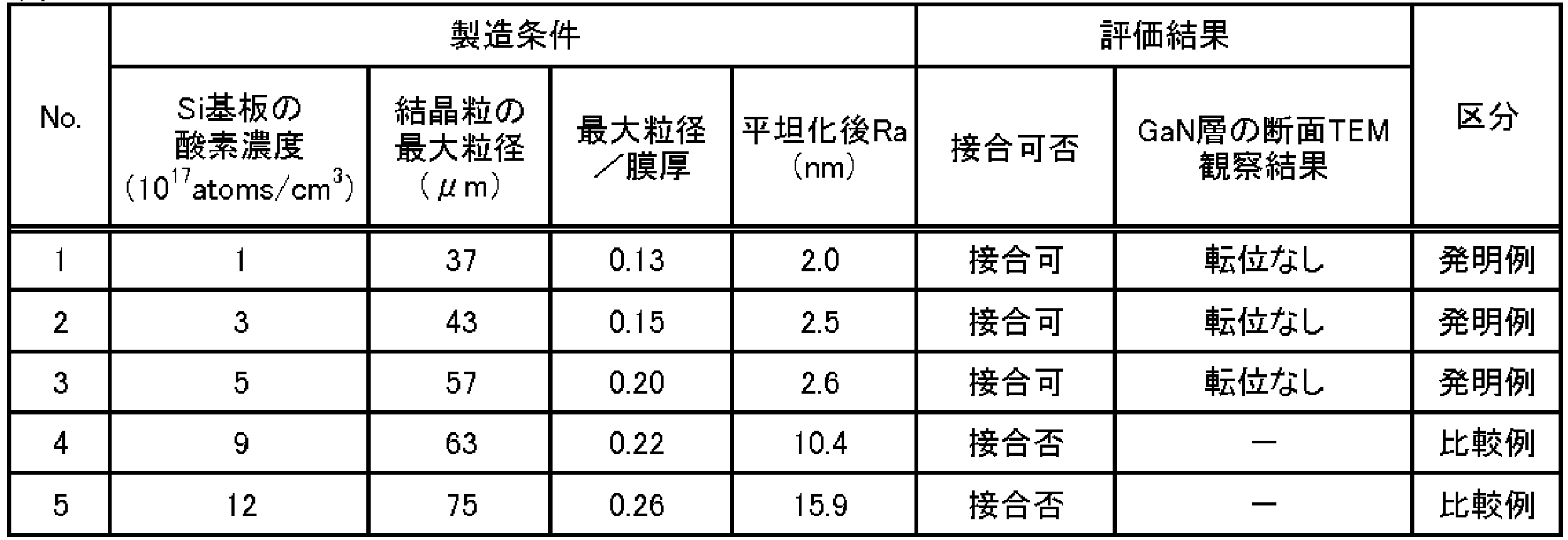
No.1~5の結果から明らかなとおり、多結晶ダイヤモンド層の表面における結晶粒の最大粒径を多結晶ダイヤモンド層の厚さで割った値が0.20以下になっていれば、プラズマ接合法によって多結晶ダイヤモンド層とGaN基板とを貼り合わせ接合できた。
(実施例3:プラズマ接合法)
多結晶ダイヤモンド層の表面にはシリコン酸化膜を形成せず、GaN基板の表面にのみ、CVD法を用いて厚さ100nmのシリコン酸化膜を形成したこと以外は、実施例2と同様の実験を行った。この際の接合可否を表3に示す。
多結晶ダイヤモンド層の表面にはシリコン酸化膜を形成せず、GaN基板の表面にのみ、CVD法を用いて厚さ100nmのシリコン酸化膜を形成したこと以外は、実施例2と同様の実験を行った。この際の接合可否を表3に示す。
接合可の発明例に関しては、GaN基板を研削及び研磨して、厚さが10μmのGaN層とした。さらに、単結晶シリコン基板を研削及び研磨して除去した。このようにして、厚さ290μmの多結晶ダイヤモンド層上に厚さが10μmのGaN層が積層された多結晶ダイヤモンド自立基板を得た。GaN層の断面をTEMにて観察したところ、表3に示すように、転位は観察されなかった。
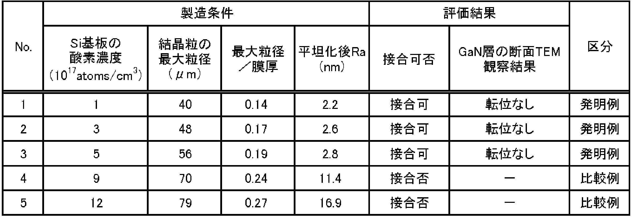
No.1~5の結果から明らかなとおり、多結晶ダイヤモンド層の表面における結晶粒の最大粒径を多結晶ダイヤモンド層の厚さで割った値が0.20以下になっていれば、プラズマ接合法によって多結晶ダイヤモンド層とGaN基板とを貼り合わせ接合できた。
(実施例4)
直径が2インチ、厚さが3mm、抵抗率が10Ω・cmで、酸素濃度が3.0×10¹⁷atoms/cm3の単結晶シリコン基板を用意した。単結晶シリコン基板上に、MOCVD法を用いてトリメチルガリウムガスとアンモニアガスを流し、1100℃にて、厚さ10μmのGaN層を形成した。次に、公知の傷付け法によって、GaN層の表面にダイヤモンド粒子を埋め込んだ。すなわち、平均粒径1μmのダイヤモンド粒子を含有する溶液中で、単結晶シリコン基板を超音波洗浄することによって、GaN層の表面にダイヤモンド粒子を埋め込んだ。次に、実施例1,2と同様の条件で、マイクロ波プラズマCVD法を用いて、GaN層上に埋め込んだダイヤモンド粒子を核として、厚さ300μmの多結晶ダイヤモンド層を成長させた。
直径が2インチ、厚さが3mm、抵抗率が10Ω・cmで、酸素濃度が3.0×10¹⁷atoms/cm3の単結晶シリコン基板を用意した。単結晶シリコン基板上に、MOCVD法を用いてトリメチルガリウムガスとアンモニアガスを流し、1100℃にて、厚さ10μmのGaN層を形成した。次に、公知の傷付け法によって、GaN層の表面にダイヤモンド粒子を埋め込んだ。すなわち、平均粒径1μmのダイヤモンド粒子を含有する溶液中で、単結晶シリコン基板を超音波洗浄することによって、GaN層の表面にダイヤモンド粒子を埋め込んだ。次に、実施例1,2と同様の条件で、マイクロ波プラズマCVD法を用いて、GaN層上に埋め込んだダイヤモンド粒子を核として、厚さ300μmの多結晶ダイヤモンド層を成長させた。
さらに、単結晶シリコン基板を研削及び研磨して除去した。このようにして、厚さ300μmの多結晶ダイヤモンド層上に厚さが10μmのGaN層が積層された多結晶ダイヤモンド自立基板を得た。しかしながら、GaN層の断面をTEMにて観察したところ、転位が観察された。
本発明の多結晶ダイヤモンド自立基板の製造方法によれば、真空常温接合法又はプラズマ接合法を用いて高品質な化合物半導体層が積層された多結晶ダイヤモンド自立基板を製造することが可能である。
100,200 多結晶ダイヤモンド自立基板
10 単結晶シリコン基板
12 ダイヤモンド粒子含有液膜
14 ダイヤモンド粒子
16 多結晶ダイヤモンド層
16A 多結晶ダイヤモンド層の表面
18 SP2領域
20 化合物半導体基板
20A 化合物半導体基板の表面
22 アモルファス層
24,24A,24B 酸化膜
26 化合物半導体層
30 貼り合わせ基板
40 貼り合わせ基板
50 真空常温接合装置
51 プラズマチャンバー
52 ガス導入口
53 真空ポンプ
54 パルス電圧印加装置
55A,55B ウェーハ固定台
10 単結晶シリコン基板
12 ダイヤモンド粒子含有液膜
14 ダイヤモンド粒子
16 多結晶ダイヤモンド層
16A 多結晶ダイヤモンド層の表面
18 SP2領域
20 化合物半導体基板
20A 化合物半導体基板の表面
22 アモルファス層
24,24A,24B 酸化膜
26 化合物半導体層
30 貼り合わせ基板
40 貼り合わせ基板
50 真空常温接合装置
51 プラズマチャンバー
52 ガス導入口
53 真空ポンプ
54 パルス電圧印加装置
55A,55B ウェーハ固定台
Claims (15)
- 単結晶シリコン基板上にダイヤモンド粒子を付着させる付着工程と、
前記ダイヤモンド粒子を核として、化学気相成長法により、前記単結晶シリコン基板上に厚さが100μm以上の多結晶ダイヤモンド層を成長させ、その際、該多結晶ダイヤモンド層の表面における結晶粒の最大粒径を前記多結晶ダイヤモンド層の厚さで割った値を0.20以下とする工程と、
前記多結晶ダイヤモンド層の表面を平坦化する平坦化工程と、
その後、真空常温接合法又はプラズマ接合法により、前記多結晶ダイヤモンド層に化合物半導体基板を貼り合わせて、貼り合わせ基板を得る工程と、
その後、前記化合物半導体基板を減厚して、化合物半導体層とする工程と、
前記貼り合わせ基板から前記単結晶シリコン基板を除去して、前記多結晶ダイヤモンド層が、前記化合物半導体層の支持基板として機能する多結晶ダイヤモンド自立基板を得る工程と、
を有することを特徴とする多結晶ダイヤモンド自立基板の製造方法。 - 前記真空常温接合法は、
前記多結晶ダイヤモンド層の表面及び前記化合物半導体基板の表面に、真空常温下でイオンビーム又は中性原子ビームを照射して、前記両方の表面を活性化面とする工程と、
引き続き真空常温下で、前記両方の活性化面を接触させることで、前記多結晶ダイヤモンド層と前記化合物半導体基板とを貼り合わせる工程と、
を有する、請求項1に記載の多結晶ダイヤモンド自立基板の製造方法。 - 前記プラズマ接合法は、
(i)前記多結晶ダイヤモンド層の表面に厚さ100nm以上1μm以下のシリコン酸化膜を形成すること、及び、(ii)前記化合物半導体基板の表面に厚さ100nm以上1μm以下のシリコン酸化膜を形成する、又は、前記化合物半導体基板を熱酸化して、その表層部に厚さ100nm以上1μm以下の酸化膜を形成すること、の少なくとも一方を行う工程と、
酸素、窒素、水素及びアルゴンの1種類以上からなる雰囲気下で、前記シリコン酸化膜及び前記酸化膜の表面と、前記多結晶ダイヤモンド層の表面及び前記化合物半導体基板の表面のうち前記シリコン酸化膜及び前記酸化膜が形成されていない表面をプラズマ処理する工程と、
前記シリコン酸化膜及び前記酸化膜を介して、前記多結晶ダイヤモンド層と前記化合物半導体基板とを重ね合わせて、雰囲気温度が300℃以上1000℃以下の熱処理を行うことで、前記多結晶ダイヤモンド層と前記化合物半導体基板とを貼り合わせる工程と、
を有する、請求項1に記載の多結晶ダイヤモンド自立基板の製造方法。 - 前記単結晶シリコン基板の酸素濃度が5×10¹⁷atoms/cm3以下である、請求項1~3のいずれか一項に記載の多結晶ダイヤモンド自立基板の製造方法。
- 前記付着工程は、前記単結晶シリコン基板上に平均粒径が50nm以下のダイヤモンド粒子を含有する溶液を塗布し、その後、前記単結晶シリコン基板に熱処理を施すことにより行う、請求項1~4のいずれか一項に記載の多結晶ダイヤモンド自立基板の製造方法。
- 前記溶液中の前記ダイヤモンド粒子が負電荷に帯電している、請求項5に記載の多結晶ダイヤモンド自立基板の製造方法。
- 前記熱処理では、前記単結晶シリコン基板の温度を100℃未満に1分以上30分以下保持する、請求項5又は6に記載の多結晶ダイヤモンド自立基板の製造方法。
- 前記平坦化工程では、前記多結晶ダイヤモンド層の表面粗さRaを3nm以下とする、請求項1~7のいずれか一項に記載の多結晶ダイヤモンド自立基板の製造方法。
- 前記化合物半導体基板は、GaN、AlN、InN、SiC、Al2O3、Ga2O3、MgO、ZnO、CdO、GaAs、GaP、GaSb、InP、InAs、InSb、又はSiGeからなる、請求項1~8のいずれか一項に記載の多結晶ダイヤモンド自立基板の製造方法。
- 前記化合物半導体層の厚さを1μm以上500μm以下とする、請求項1~9のいずれか一項に記載の多結晶ダイヤモンド自立基板の製造方法。
- 厚さが100μm以上の多結晶ダイヤモンド層からなる支持基板と、
前記多結晶ダイヤモンド層の表面上に形成された化合物半導体層と、
を有し、前記多結晶ダイヤモンド層の表面における結晶粒の最大粒径を前記多結晶ダイヤモンド層の厚さで割った値が0.20以下であることを特徴とする多結晶ダイヤモンド自立基板。 - 前記多結晶ダイヤモンド層の表面と前記化合物半導体層との間に、合計厚さが2nm以上10nm以下の、ダイヤモンドのアモルファス層及び前記化合物半導体層を構成する化合物半導体のアモルファス層を有する、請求項11に記載の多結晶ダイヤモンド自立基板。
- 前記多結晶ダイヤモンド層の表面と前記化合物半導体層との間に、合計厚さが200nm以上2μm以下の、シリコン酸化膜及び前記化合物半導体層を構成する化合物半導体の酸化膜の少なくとも一方を有する、請求項11に記載の多結晶ダイヤモンド自立基板。
- 前記化合物半導体層は、GaN、AlN、InN、SiC、Al2O3、Ga2O3、MgO、ZnO、CdO、GaAs、GaP、GaSb、InP、InAs、InSb、又はSiGeからなる、請求項11~13のいずれか一項に記載の多結晶ダイヤモンド自立基板。
- 前記化合物半導体層の厚さが1μm以上500μm以下である、請求項11~14のいずれか一項に記載の多結晶ダイヤモンド自立基板。
Priority Applications (2)
| Application Number | Priority Date | Filing Date | Title |
|---|---|---|---|
| CN201980086235.8A CN113557588B (zh) | 2018-12-25 | 2019-09-25 | 多晶金刚石自立基板及其制造方法 |
| DE112019006396.0T DE112019006396B4 (de) | 2018-12-25 | 2019-09-25 | Freistehendes polykristallines diamantsubstrat und verfahren zur herstellung desselben |
Applications Claiming Priority (2)
| Application Number | Priority Date | Filing Date | Title |
|---|---|---|---|
| JP2018-241750 | 2018-12-25 | ||
| JP2018241750A JP7115297B2 (ja) | 2018-12-25 | 2018-12-25 | 多結晶ダイヤモンド自立基板及びその製造方法 |
Publications (1)
| Publication Number | Publication Date |
|---|---|
| WO2020137052A1 true WO2020137052A1 (ja) | 2020-07-02 |
Family
ID=71127916
Family Applications (1)
| Application Number | Title | Priority Date | Filing Date |
|---|---|---|---|
| PCT/JP2019/037652 Ceased WO2020137052A1 (ja) | 2018-12-25 | 2019-09-25 | 多結晶ダイヤモンド自立基板及びその製造方法 |
Country Status (4)
| Country | Link |
|---|---|
| JP (1) | JP7115297B2 (ja) |
| CN (1) | CN113557588B (ja) |
| DE (1) | DE112019006396B4 (ja) |
| WO (1) | WO2020137052A1 (ja) |
Cited By (6)
| Publication number | Priority date | Publication date | Assignee | Title |
|---|---|---|---|---|
| CN111850334A (zh) * | 2020-07-17 | 2020-10-30 | 苏州思珀利尔工业技术有限公司 | 聚晶金刚石微粉的制备方法、聚晶金刚石微粉及应用 |
| CN113113306A (zh) * | 2021-04-08 | 2021-07-13 | 绍兴同芯成集成电路有限公司 | 一种利用耐高温托盘进行化合物半导体晶圆高温回火工艺 |
| EP4002430A1 (en) * | 2020-11-11 | 2022-05-25 | Sumco Corporation | Bonded wafer and method of producing bonded wafer |
| JPWO2024004314A1 (ja) * | 2022-06-30 | 2024-01-04 | ||
| WO2025070739A1 (ja) * | 2023-09-28 | 2025-04-03 | 日本碍子株式会社 | 複合ウエハーおよび複合ウエハーの製造方法 |
| CN119932515A (zh) * | 2023-11-03 | 2025-05-06 | 湖南新锋科技有限公司 | 一种金刚石颗粒镶嵌金属基金刚石涂层复合材料及其制备方法与应用 |
Families Citing this family (4)
| Publication number | Priority date | Publication date | Assignee | Title |
|---|---|---|---|---|
| CN112376034B (zh) * | 2020-10-26 | 2021-09-07 | 北京科技大学 | 一种带光学增透膜的金刚石制备方法 |
| JP7480699B2 (ja) * | 2020-12-24 | 2024-05-10 | 株式会社Sumco | 多結晶ダイヤモンド自立基板を用いた積層基板及びその製造方法 |
| CN112760612B (zh) * | 2020-12-28 | 2022-07-01 | 吉林工程技术师范学院 | 一种自支撑纳米针多孔金刚石的制备方法 |
| JP7810099B2 (ja) | 2022-11-29 | 2026-02-03 | 信越半導体株式会社 | ヘテロエピタキシャル基板の製造方法 |
Citations (3)
| Publication number | Priority date | Publication date | Assignee | Title |
|---|---|---|---|---|
| JP2018049868A (ja) * | 2016-09-20 | 2018-03-29 | 住友電気工業株式会社 | 半導体積層構造体および半導体デバイス |
| JP2018074172A (ja) * | 2013-09-02 | 2018-05-10 | アールエフエイチアイシー コーポレイション | 基板近傍の熱伝導性が改善された多結晶性cvdダイヤモンドを含む半導体デバイス構造体 |
| WO2018143344A1 (ja) * | 2017-02-02 | 2018-08-09 | 三菱電機株式会社 | 半導体製造方法および半導体製造装置 |
Family Cites Families (6)
| Publication number | Priority date | Publication date | Assignee | Title |
|---|---|---|---|---|
| JP5978548B2 (ja) | 2012-02-29 | 2016-08-24 | エレメント シックス テクノロジーズ ユーエス コーポレイション | ダイヤモンド上の窒化ガリウム型ウェーハの製造方法 |
| JP6049571B2 (ja) | 2013-08-28 | 2016-12-21 | 信越化学工業株式会社 | 窒化物半導体薄膜を備えた複合基板の製造方法 |
| WO2015199180A1 (ja) * | 2014-06-25 | 2015-12-30 | 住友電気工業株式会社 | ダイヤモンド基板の製造方法、ダイヤモンド基板、及び、ダイヤモンド複合基板 |
| JP6257575B2 (ja) * | 2015-11-25 | 2018-01-10 | 株式会社アライドマテリアル | 半導体パッケージ、及び半導体装置 |
| JP2019153603A (ja) * | 2016-07-19 | 2019-09-12 | 三菱電機株式会社 | 半導体基板及びその製造方法 |
| JP6604300B2 (ja) * | 2016-10-14 | 2019-11-13 | 株式会社Sumco | シリコン接合ウェーハの製造方法 |
-
2018
- 2018-12-25 JP JP2018241750A patent/JP7115297B2/ja active Active
-
2019
- 2019-09-25 WO PCT/JP2019/037652 patent/WO2020137052A1/ja not_active Ceased
- 2019-09-25 CN CN201980086235.8A patent/CN113557588B/zh active Active
- 2019-09-25 DE DE112019006396.0T patent/DE112019006396B4/de active Active
Patent Citations (3)
| Publication number | Priority date | Publication date | Assignee | Title |
|---|---|---|---|---|
| JP2018074172A (ja) * | 2013-09-02 | 2018-05-10 | アールエフエイチアイシー コーポレイション | 基板近傍の熱伝導性が改善された多結晶性cvdダイヤモンドを含む半導体デバイス構造体 |
| JP2018049868A (ja) * | 2016-09-20 | 2018-03-29 | 住友電気工業株式会社 | 半導体積層構造体および半導体デバイス |
| WO2018143344A1 (ja) * | 2017-02-02 | 2018-08-09 | 三菱電機株式会社 | 半導体製造方法および半導体製造装置 |
Cited By (9)
| Publication number | Priority date | Publication date | Assignee | Title |
|---|---|---|---|---|
| CN111850334A (zh) * | 2020-07-17 | 2020-10-30 | 苏州思珀利尔工业技术有限公司 | 聚晶金刚石微粉的制备方法、聚晶金刚石微粉及应用 |
| EP4002430A1 (en) * | 2020-11-11 | 2022-05-25 | Sumco Corporation | Bonded wafer and method of producing bonded wafer |
| CN113113306A (zh) * | 2021-04-08 | 2021-07-13 | 绍兴同芯成集成电路有限公司 | 一种利用耐高温托盘进行化合物半导体晶圆高温回火工艺 |
| CN113113306B (zh) * | 2021-04-08 | 2024-05-28 | 绍兴同芯成集成电路有限公司 | 一种利用耐高温托盘进行化合物半导体晶圆高温回火工艺 |
| JPWO2024004314A1 (ja) * | 2022-06-30 | 2024-01-04 | ||
| WO2024004314A1 (ja) * | 2022-06-30 | 2024-01-04 | 日本碍子株式会社 | 複合基板および13族元素窒化物エピタキシャル成長用基板 |
| JP7710614B2 (ja) | 2022-06-30 | 2025-07-18 | 日本碍子株式会社 | 複合基板および13族元素窒化物エピタキシャル成長用基板 |
| WO2025070739A1 (ja) * | 2023-09-28 | 2025-04-03 | 日本碍子株式会社 | 複合ウエハーおよび複合ウエハーの製造方法 |
| CN119932515A (zh) * | 2023-11-03 | 2025-05-06 | 湖南新锋科技有限公司 | 一种金刚石颗粒镶嵌金属基金刚石涂层复合材料及其制备方法与应用 |
Also Published As
| Publication number | Publication date |
|---|---|
| CN113557588A (zh) | 2021-10-26 |
| CN113557588B (zh) | 2024-05-31 |
| DE112019006396B4 (de) | 2022-11-24 |
| DE112019006396T5 (de) | 2021-09-02 |
| JP7115297B2 (ja) | 2022-08-09 |
| JP2020102598A (ja) | 2020-07-02 |
Similar Documents
| Publication | Publication Date | Title |
|---|---|---|
| JP7115297B2 (ja) | 多結晶ダイヤモンド自立基板及びその製造方法 | |
| US10784146B2 (en) | Method of depositing charge trapping polycrystalline silicon films on silicon substrates with controllable film stress | |
| US10381261B2 (en) | Method of manufacturing high resistivity semiconductor-on-insulator wafers with charge trapping layers | |
| TWI721223B (zh) | 具有較佳電荷捕獲效率之高電阻率絕緣體上矽基板 | |
| US11139198B2 (en) | High resistivity semiconductor-on-insulator wafer and a method of manufacturing | |
| CN113544318B (zh) | 多晶金刚石自立基板的制造方法 | |
| US20240258155A1 (en) | Methods of manufacturing semiconductor-on-insulator wafers having charge trapping layers with controlled stress | |
| EP3656896B1 (en) | Method for producing diamond laminated silicon wafer, and diamond laminated silicon wafer | |
| JP6772995B2 (ja) | Soiウェーハの製造方法およびsoiウェーハ | |
| CN117038572A (zh) | 绝缘体上半导体结构的制造方法 | |
| JP7835188B2 (ja) | 半導体基板の製造方法 | |
| JP2023085098A (ja) | 積層ウェーハ及びその製造方法 | |
| JPH0870111A (ja) | 半導体基板の作製方法及び半導体基板 |
Legal Events
| Date | Code | Title | Description |
|---|---|---|---|
| 121 | Ep: the epo has been informed by wipo that ep was designated in this application |
Ref document number: 19902585 Country of ref document: EP Kind code of ref document: A1 |
|
| 122 | Ep: pct application non-entry in european phase |
Ref document number: 19902585 Country of ref document: EP Kind code of ref document: A1 |