WO2020122137A1 - Iii族窒化物半導体発光素子及びその製造方法 - Google Patents
Iii族窒化物半導体発光素子及びその製造方法 Download PDFInfo
- Publication number
- WO2020122137A1 WO2020122137A1 PCT/JP2019/048537 JP2019048537W WO2020122137A1 WO 2020122137 A1 WO2020122137 A1 WO 2020122137A1 JP 2019048537 W JP2019048537 W JP 2019048537W WO 2020122137 A1 WO2020122137 A1 WO 2020122137A1
- Authority
- WO
- WIPO (PCT)
- Prior art keywords
- layer
- type
- light emitting
- contact layer
- group iii
- Prior art date
- Legal status (The legal status is an assumption and is not a legal conclusion. Google has not performed a legal analysis and makes no representation as to the accuracy of the status listed.)
- Ceased
Links
Images

Classifications
-
- H—ELECTRICITY
- H10—SEMICONDUCTOR DEVICES; ELECTRIC SOLID-STATE DEVICES NOT OTHERWISE PROVIDED FOR
- H10H—INORGANIC LIGHT-EMITTING SEMICONDUCTOR DEVICES HAVING POTENTIAL BARRIERS
- H10H20/00—Individual inorganic light-emitting semiconductor devices having potential barriers, e.g. light-emitting diodes [LED]
- H10H20/80—Constructional details
- H10H20/81—Bodies
- H10H20/816—Bodies having carrier transport control structures, e.g. highly-doped semiconductor layers or current-blocking structures
- H10H20/8162—Current-blocking structures
-
- H—ELECTRICITY
- H10—SEMICONDUCTOR DEVICES; ELECTRIC SOLID-STATE DEVICES NOT OTHERWISE PROVIDED FOR
- H10H—INORGANIC LIGHT-EMITTING SEMICONDUCTOR DEVICES HAVING POTENTIAL BARRIERS
- H10H20/00—Individual inorganic light-emitting semiconductor devices having potential barriers, e.g. light-emitting diodes [LED]
- H10H20/01—Manufacture or treatment
- H10H20/011—Manufacture or treatment of bodies, e.g. forming semiconductor layers
- H10H20/013—Manufacture or treatment of bodies, e.g. forming semiconductor layers having light-emitting regions comprising only Group III-V materials
- H10H20/0133—Manufacture or treatment of bodies, e.g. forming semiconductor layers having light-emitting regions comprising only Group III-V materials with a substrate not being Group III-V materials
- H10H20/01335—Manufacture or treatment of bodies, e.g. forming semiconductor layers having light-emitting regions comprising only Group III-V materials with a substrate not being Group III-V materials the light-emitting regions comprising nitride materials
-
- H—ELECTRICITY
- H10—SEMICONDUCTOR DEVICES; ELECTRIC SOLID-STATE DEVICES NOT OTHERWISE PROVIDED FOR
- H10H—INORGANIC LIGHT-EMITTING SEMICONDUCTOR DEVICES HAVING POTENTIAL BARRIERS
- H10H20/00—Individual inorganic light-emitting semiconductor devices having potential barriers, e.g. light-emitting diodes [LED]
- H10H20/01—Manufacture or treatment
- H10H20/011—Manufacture or treatment of bodies, e.g. forming semiconductor layers
- H10H20/013—Manufacture or treatment of bodies, e.g. forming semiconductor layers having light-emitting regions comprising only Group III-V materials
- H10H20/0137—Manufacture or treatment of bodies, e.g. forming semiconductor layers having light-emitting regions comprising only Group III-V materials the light-emitting regions comprising nitride materials
-
- H—ELECTRICITY
- H10—SEMICONDUCTOR DEVICES; ELECTRIC SOLID-STATE DEVICES NOT OTHERWISE PROVIDED FOR
- H10H—INORGANIC LIGHT-EMITTING SEMICONDUCTOR DEVICES HAVING POTENTIAL BARRIERS
- H10H20/00—Individual inorganic light-emitting semiconductor devices having potential barriers, e.g. light-emitting diodes [LED]
- H10H20/80—Constructional details
- H10H20/81—Bodies
- H10H20/811—Bodies having quantum effect structures or superlattices, e.g. tunnel junctions
- H10H20/812—Bodies having quantum effect structures or superlattices, e.g. tunnel junctions within the light-emitting regions, e.g. having quantum confinement structures
-
- H—ELECTRICITY
- H10—SEMICONDUCTOR DEVICES; ELECTRIC SOLID-STATE DEVICES NOT OTHERWISE PROVIDED FOR
- H10H—INORGANIC LIGHT-EMITTING SEMICONDUCTOR DEVICES HAVING POTENTIAL BARRIERS
- H10H20/00—Individual inorganic light-emitting semiconductor devices having potential barriers, e.g. light-emitting diodes [LED]
- H10H20/80—Constructional details
- H10H20/81—Bodies
- H10H20/822—Materials of the light-emitting regions
- H10H20/824—Materials of the light-emitting regions comprising only Group III-V materials, e.g. GaP
- H10H20/825—Materials of the light-emitting regions comprising only Group III-V materials, e.g. GaP containing nitrogen, e.g. GaN
-
- H—ELECTRICITY
- H10—SEMICONDUCTOR DEVICES; ELECTRIC SOLID-STATE DEVICES NOT OTHERWISE PROVIDED FOR
- H10H—INORGANIC LIGHT-EMITTING SEMICONDUCTOR DEVICES HAVING POTENTIAL BARRIERS
- H10H20/00—Individual inorganic light-emitting semiconductor devices having potential barriers, e.g. light-emitting diodes [LED]
- H10H20/80—Constructional details
- H10H20/83—Electrodes
- H10H20/832—Electrodes characterised by their material
-
- H—ELECTRICITY
- H10—SEMICONDUCTOR DEVICES; ELECTRIC SOLID-STATE DEVICES NOT OTHERWISE PROVIDED FOR
- H10H—INORGANIC LIGHT-EMITTING SEMICONDUCTOR DEVICES HAVING POTENTIAL BARRIERS
- H10H20/00—Individual inorganic light-emitting semiconductor devices having potential barriers, e.g. light-emitting diodes [LED]
- H10H20/80—Constructional details
- H10H20/83—Electrodes
- H10H20/832—Electrodes characterised by their material
- H10H20/835—Reflective materials
-
- H—ELECTRICITY
- H10—SEMICONDUCTOR DEVICES; ELECTRIC SOLID-STATE DEVICES NOT OTHERWISE PROVIDED FOR
- H10H—INORGANIC LIGHT-EMITTING SEMICONDUCTOR DEVICES HAVING POTENTIAL BARRIERS
- H10H20/00—Individual inorganic light-emitting semiconductor devices having potential barriers, e.g. light-emitting diodes [LED]
- H10H20/01—Manufacture or treatment
- H10H20/032—Manufacture or treatment of electrodes
-
- H—ELECTRICITY
- H10—SEMICONDUCTOR DEVICES; ELECTRIC SOLID-STATE DEVICES NOT OTHERWISE PROVIDED FOR
- H10H—INORGANIC LIGHT-EMITTING SEMICONDUCTOR DEVICES HAVING POTENTIAL BARRIERS
- H10H20/00—Individual inorganic light-emitting semiconductor devices having potential barriers, e.g. light-emitting diodes [LED]
- H10H20/80—Constructional details
- H10H20/81—Bodies
- H10H20/811—Bodies having quantum effect structures or superlattices, e.g. tunnel junctions
Definitions
- the present invention relates to a group III nitride semiconductor light emitting device and a method for manufacturing the same, and more particularly to a group III nitride semiconductor light emitting device and a method for manufacturing the same that achieve both high light emission output and excellent reliability.
- Group III nitride semiconductors composed of compounds of group III elements such as Al, Ga, In and N are wide bandgap semiconductors having a direct transition band structure, and are used for sterilization, water purification, medical treatment, illumination, high density optical recording. It is a material that is expected to have a wide range of application fields such as.
- a light-emitting device using a group III nitride semiconductor in the light-emitting layer can cover from the deep ultraviolet light to the visible light region by adjusting the content ratio of the group III element, and is practically used for various light sources. Is being promoted.
- a deep ultraviolet light emitting device that emits deep ultraviolet light is generally manufactured as follows. That is, a buffer layer is formed on a substrate such as sapphire or AlN single crystal, and an n-type semiconductor layer, a light emitting layer, and a p-type semiconductor layer made of a group III nitride semiconductor are sequentially formed. Next, an n-side electrode electrically connected to the n-type semiconductor layer and a p-side electrode electrically connected to the p-type semiconductor layer are formed.
- a p-type GaN contact layer that easily increases the hole concentration.
- the p-type GaN contact layer absorbs light having a wavelength of 360 nm or less due to its band gap.
- Patent Document 1 discloses a group III nitride semiconductor device in which a GaN layer having a film thickness of 0.01 ⁇ m or more and 0.3 ⁇ m or less is provided on an AlGaInN layer having a relatively high Al composition ratio.
- the growth mode of the GaN layer is grown in a state close to an FM (Frank-van-der-Merwe) mode (pseudo FM mode), so that the surface of the GaN layer is smoothed immediately after crystal growth.
- the surface can be made smooth even when the GaN layer formed on the AlGaInN layer having a high Al composition ratio is thinned.
- the film thickness of the p-type GaN contact layer can be reduced, so that light absorption by the layer can be suppressed and the light extraction efficiency of the group III nitride semiconductor device can be improved. Expected to be possible.
- a sample of the group III nitride semiconductor light-emitting device having an emission area of 0.057 mm 2 was energized at 20 mA to measure the initial light emission output, then energized at 100 mA for 3 seconds, and then measured again at 20 mA.
- the sample in which the output decrease of more than half of the initial light emission output is confirmed has caused death.
- the above-mentioned 20 mA is a current value within a range where linearity is maintained
- the above-mentioned 100 mA is the light emitting device.
- an object of the present invention is to provide a group III nitride semiconductor light emitting device that achieves both high light emission output and excellent reliability, and a method for manufacturing the same.
- the present inventors diligently studied how to solve the above problems.
- the p-type GaN layer is formed to be as thin as 50 nm or less, defects are introduced and surface flatness deteriorates due to the large relaxation of compressive strain.
- the p-type GaN layer is grown in the FM mode, if the AlGaN layer (AlInGaN layer in the case of containing In) that is directly under the p-type GaN layer has irregularities or dislocations, the growth proceeds in the direction of embedding it. It is speculated that the relaxation of the compressive strain is likely to proceed and defects are likely to be introduced.
- the present inventor considered that the light emitting elements die when they are in the electrode formation region. Therefore, it was found that by using an AlGaN layer having an Al composition ratio x of 0.03 or more and 0.25 or less as the p-type contact layer, it is possible to prevent death of the light emitting element and achieve both high light emission output and excellent reliability. Then, the present invention has been completed. That is, the gist of the present invention is as follows.
- a Group III nitride semiconductor light-emitting device which comprises an n-type semiconductor layer, a light-emitting layer, a p-type AlGaN electron blocking layer, a p-type contact layer, and a p-side reflective electrode on a substrate in this order.
- the emission center wavelength of the light emitted from the light emitting layer is 250 nm or more and 330 nm or less
- the Al composition ratio of the p-type AlGaN electron block layer is 0.40 or more and 0.80 or less
- the p-type contact layer has a film thickness of 10 nm or more and 50 nm or less
- the p-type contact layer has a p-type AlGaN contact layer having an Al composition ratio of 0.03 or more and 0.25 or less.
- Group III nitride semiconductor light emitting device is
- a step of forming an n-type semiconductor layer on the substrate Forming a light emitting layer on the n-type semiconductor layer; Forming a p-type AlGaN electron blocking layer on the light emitting layer; Forming a p-type contact layer on the p-type AlGaN electron blocking layer; And a step of forming a p-side reflective electrode on the p-type contact layer, the method including the steps of:
- the emission center wavelength from the light emitting layer is 250 nm or more and 330 nm or less,
- the Al composition ratio of the p-type AlGaN electron block layer is 0.40 or more and 0.80 or less,
- the thickness of the p-type contact layer is 10 nm or more and 50 nm or less,
- a method for manufacturing a group III nitride semiconductor light emitting device wherein the p-type contact layer is a p-type AlGaN contact layer having an Al composition ratio of 0.03 or more and 0.25 or less.
- FIG. 3 is a schematic cross-sectional view illustrating one embodiment of a group III nitride semiconductor light emitting device according to the present invention.
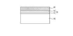
- FIG. 3 is an enlarged schematic cross-sectional view illustrating one aspect of the p-type contact layer of the group III nitride semiconductor light emitting device according to the present invention.
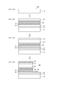
- FIG. 3 is a schematic cross-sectional view illustrating one embodiment of a method for manufacturing a Group III nitride semiconductor light emitting device according to the present invention.
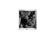
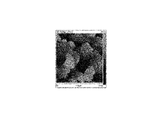
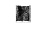
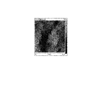
- 3 is an AFM image of the surface of the p-type contact layer of Example 1.
- 3 is an AFM image of the surface of the p-type contact layer of Example 2.
- 6 is an AFM image of the surface of the p-type contact layer of Example 3.
- 5 is an AFM image of the surface of the p-type contact layer of Comparative Example 1.
- AlGaN the composition ratio of the group III element (total of Al and Ga) and N is 1:1 and the group III element is The ratio of Al and Ga means any arbitrary compound.
- AlGaN may include 5% or less of In with respect to the total of Al and Ga as Group III elements, even if there is no description about In which is a Group III element.
- the Al composition ratio is x and the In composition ratio is y (0 ⁇ y ⁇ 0.05), and Al x In y Ga 1 ⁇ x ⁇ y N.
- AlN When simply expressed as “AlN” or “GaN”, it means that Ga and Al are not included, respectively, but unless otherwise specified, simply expressed as “AlGaN” means either AlN or GaN. It does not exclude that.
- the value of the Al composition ratio can be measured by photoluminescence measurement, X-ray diffraction measurement, or the like.
- a layer that electrically functions as p-type is referred to as a p-type layer
- a layer that electrically functions as n-type is referred to as an n-type layer.
- a specific impurity such as Mg or Si is not intentionally added and does not electrically function as p-type or n-type, it is referred to as “i-type” or “undoped”.
- the undoped layer may contain impurities that are unavoidable during the manufacturing process. Specifically, when the carrier density is low (for example, less than 4 ⁇ 10 16 /cm 3 ), it is referred to as “undoped” in the present specification.
- the value of the impurity concentration of Mg, Si, etc. is based on SIMS analysis.
- the total film thickness of each layer formed by epitaxial growth can be measured using an optical interference type film thickness meter.
- the film thickness of each layer can be calculated by observing the cross section of the growth layer with a transmission electron microscope when the composition of each adjacent layer is sufficiently different (for example, when the Al composition ratio is different by 0.01 or more). Further, regarding the boundary and the film thickness of the layers having the same Al composition ratio or almost the same (for example, the Al composition ratio is less than 0.01) among the adjacent layers but different impurity concentrations, the boundary between the two Also, the film thickness of each layer shall be measured by TEM-EDS. The impurity concentrations of both can be measured by SIMS analysis. In addition, when the film thickness of each layer is thin like a superlattice structure, the film thickness can be measured using TEM-EDS.
- a group III nitride semiconductor light emitting device 100 includes an n-type semiconductor layer 30, a light emitting layer 40, a p-type AlGaN electron block layer 60, and a p-type contact on a substrate 10.
- the layer 70 and the p-side reflective electrode 80 are sequentially provided.
- the emission center wavelength of light emitted from the light emitting layer 40 is 250 nm or more and 330 nm or less
- the Al composition ratio of the p-type AlGaN electron block layer 60 is 0.40 or more and 0.80 or less
- the film of the p-type contact layer 70 is The thickness is 10 nm or more and 50 nm or less
- the p-type contact layer 70 has a p-type AlGaN contact layer 71 having an Al composition ratio of 0.03 or more and 0.25 or less.
- a buffer layer 20 is provided between the substrate 10 and the n-type semiconductor layer 30, an exposed surface is provided on the n-type semiconductor layer 30, and an n-side electrode 90 is provided on the exposed surface.
- a sapphire substrate can be used as the substrate 10 of the group III nitride semiconductor light emitting device 100.
- An AlN template substrate having an AlN layer epitaxially grown on the surface of the sapphire substrate may be used.
- any sapphire substrate can be used, and the presence or absence of the off angle is arbitrary. When the off angle is provided, the crystal axis orientation in the tilt direction is either the m-axis direction or the a-axis direction. But it's okay.
- the main surface of the sapphire substrate can be a surface in which the C surface is inclined at an off angle ⁇ of 0.5 degrees.
- the crystallinity of the AlN layer on the surface of the sapphire substrate is excellent. It is also preferable that an undoped AlGaN layer is provided on the surface of the AlN template substrate. Alternatively, an AlN single crystal substrate may be used as the substrate 10.
- the n-type semiconductor layer 30 is provided on the substrate 10 via the buffer layer 20 if necessary.
- the n-type semiconductor layer 30 may be directly provided on the substrate 10.
- AlGaN doped with an n-type dopant can be used.
- a group III element such as In may be introduced at a composition ratio within 5% to obtain AlGaInN or the like.
- Specific examples of the n-type dopant include silicon (Si), germanium (Ge), tin (Sn), sulfur (S), oxygen (O), titanium (Ti), zirconium (Zr), and the like.
- the dopant concentration of the n-type dopant is not particularly limited as long as the n-type semiconductor layer 30 can function as an n-type, and is, for example, 1.0 ⁇ 10 18 atoms/cm 3 to 1.0 ⁇ 10 20. It may be atoms/cm 3 .
- the band gap of the n-type semiconductor layer 30 is wider than the band gap of the light emitting layer 40 (the well layer 41 in the case of a quantum well structure), and it is preferable that the n type semiconductor layer 30 is transparent to the emitted deep ultraviolet light.
- the n-type semiconductor layer 30 may have a single-layer structure or a structure having a plurality of layers, as well as a composition-graded layer in which the composition ratio of Group III elements is compositionally graded in the crystal growth direction, or a superlattice structure.
- the n-type semiconductor layer 30 can not only form a contact portion with the n-side electrode 90 but also have a function of enhancing crystallinity from the substrate to the light emitting layer.
- the light emitting layer 40 is provided on the n-type semiconductor layer 30, and emits deep ultraviolet light having an emission center wavelength of 250 nm or more and 330 nm or less.
- the light emitting layer 40 may be made of AlGaN, and the Al composition ratio thereof may be appropriately set so as to obtain a desired emission center wavelength, and may be set in the range of 0.17 to 0.70, for example.
- the light emitting layer 40 may have a single-layer structure with a constant Al composition ratio, or a multiple quantum well (MQW: Multiple Quantum Well) in which a well layer 41 and a barrier layer 42 made of AlGaN having different Al composition ratios are repeatedly formed. It is also preferable to construct the structure.
- a group III element such as In may be introduced at a composition ratio within 5% to form an AlGaInN material or the like, but a ternary system using only Al and Ga as the group III element It is more preferable to use the AlGaN material.
- the Al composition ratio b of the barrier layer 42 is made higher than the Al composition ratio w of the well layer 41 (that is, b>w).
- the Al composition ratio b of the barrier layer 42 can be set to 0.30 to 0.95, for example.
- the center emission wavelength can be substantially adjusted by the Al composition ratio w of the well layer 41. For example, when the Al composition ratio w of the well layer 41 in the light emitting layer 40 is 0.17 to 0.68, the light is emitted from the light emitting layer 40.
- the center wavelength of the emitted light is 250 to 330 nm.
- the number of repetitions of the well layer 41 and the barrier layer 42 is not particularly limited and can be set to 1 to 10 times, for example. It is preferable that both ends (that is, the first and last) of the light emitting layer 40 in the film thickness direction be barrier layers, and when the number of repetitions of the well layer 41 and the barrier layer 42 is n, in this case, “n. Layer and barrier layer”. Further, the film thickness of the well layer 41 can be 0.5 nm to 5 nm, and the film thickness of the barrier layer 42 can be 3 nm to 30 nm.
- the conductivity type of the barrier layer 42 is preferably n-type. This is because the electron concentration is increased and there is an effect of compensating for crystal defects in the well layer 41.
- the light emitting layer 40 may have a general multiple quantum well (MQW) structure in which the barrier layer 42 and the well layer 41 are repeatedly formed and sandwiched between the barrier layers 42, and if necessary, p The final barrier layer 42 on the type AlGaN electron block layer 60 side may be removed.
- MQW multiple quantum well
- the p-type AlGaN electron blocking layer 60 is provided on the light emitting layer 40.
- the p-type AlGaN electron block layer 60 is used as a layer for blocking electrons and injecting the electrons into the light emitting layer 40 (the well layer 41 in the case of the MQW structure) to improve the electron injection efficiency.
- p-type AlGaN electron block layer p-type Al z Ga 1-z N (0.40 ⁇ z ⁇ 0.80) having an Al composition ratio of 0.40 or more and 0.80 or less is used. Can be used.
- a quaternary AlGaInN material into which a group III element such as In is introduced at a composition ratio of 5% or less may be used, but a ternary system AlGaN using only Al and Ga as the group III element is used.
- the material is more preferable.
- the Al composition ratio is in this range, a relatively large number of dislocations are formed in the p-type AlGaN electron block layer 60. Therefore, in such a case, it is effective to use the p-type contact layer 70 according to the present invention.
- the Al composition ratio is 0.60 or more and 0.70 or less, dislocations are particularly likely to be formed.
- the thickness of the p-type AlGaN electron block layer 60 is not particularly limited, but is preferably 10 nm to 80 nm, for example. When the film thickness of the p-type AlGaN electron block layer 60 is in this range, a high light emission output can be reliably obtained.
- the film thickness of the p-type AlGaN electron block layer 60 is preferably larger than the film thickness of the barrier layer 42.
- Examples of the p-type dopant with which the p-type AlGaN electron blocking layer 60 is doped include magnesium (Mg), zinc (Zn), calcium (Ca), beryllium (Be), and manganese (Mn). It is common to use Mg.
- the dopant concentration of the p-type AlGaN electron blocking layer 60 is not particularly limited as long as it is a dopant concentration that can function as a p-type layer, and is, for example, 1.0 ⁇ 10 18 atoms/cm 3 to 5.0 ⁇ 10 21 atoms. /Cm 3 can be used.
- the p-type contact layer 70 is directly provided on the p-type AlGaN electron block layer 60.
- the p-type contact layer 70 is a layer for reducing the contact resistance between the p-side reflective electrode 80 provided on the outermost surface thereof and the p-type AlGaN electron block layer 60.
- the film thickness of the p-type contact layer 70 is 10 nm or more and 50 nm or less.
- the p-type contact layer 70 has a p-type AlGaN layer 71 having an Al composition ratio x of 0.03 or more and 0.25 or less.
- the p-type AlGaN contact layer 71 is formed immediately above the p-type AlGaN electron block layer 60, and the Al composition ratio x of the composition formula Al x Ga 1-x N is 0.03 ⁇ x ⁇ 0.25. be able to. It has been confirmed by experiments by the present inventors that the p-type contact layer 70 has the p-type AlGaN layer 71 directly above the p-type AlGaN electron blocking layer 60, thereby preventing death of the group III nitride semiconductor light emitting device 100.
- a p-type AlGaN contact layer 71 (Al x Ga 1-x N, 0.03 ⁇ x ⁇ 0.25) was formed. It is considered that this is because the generation of dislocations formed in the initial stage of growth can be suppressed while suppressing the adverse effect of the deterioration of surface flatness.
- the p-type contact layer 70 has the above-mentioned p-type AlGaN contact layer 71 directly above the p-type AlGaN electron block layer 60.
- the p-type contact layer 70 may be composed of only the p-type AlGaN contact layer 71 (see FIG. 1), while the p-type contact layer 70 includes the p-type AlGaN contact layer 71 and the p-side reflective electrode 80. You may have a p-type GaN contact layer between them (refer FIG. 2).
- the film thickness of the p-type AlGaN contact layer 71 can be 10 nm or more and 50 nm or less, and the p-type contact layer 70 as a whole may have the film thickness of 10 nm or more and 50 nm or less.
- the film thickness of the p-type AlGaN contact layer 71 is 10 nm or more and 25 nm or less.
- the thickness of the p-type contact layer 70 is 15 nm or more in order to more surely suppress the death to zero.
- the p-type contact layer 70 has a Mg concentration of 3 ⁇ 10 20 atoms/cm 3 on the side opposite to the p-type AlGaN electron block layer 60 (in other words, the side in contact with the p-side reflective electrode 80). It is preferable to have the above-mentioned high-concentration region, and it is more preferable that the Mg concentration in this high-concentration region is 5 ⁇ 10 20 atoms/cm 3 or more. By increasing the hole concentration of the p-type contact layer 70, the forward voltage Vf of the group III nitride semiconductor light emitting device 100 can be lowered.
- the upper limit of the Mg concentration in the high concentration region can be set to 1 ⁇ 10 21 atoms/cm 3 in the present embodiment.
- the Mg concentration in the region of the p-type contact layer 70 on the p-type AlGaN electron block layer 60 side can be set in a general range, and is usually 5 ⁇ 10 19 atoms/cm 3 or more and 3 ⁇ 10 20 atoms/cm 3. It is less than 3 .
- the Mg concentration in the p-type contact layer is an average concentration in each region measured by SIMS.
- the film thickness in the high concentration region is usually 15 nm or less.
- the p-side reflective electrode 80 can be provided directly on the p-type contact layer 70 (on the outermost surface).
- a metal having a high reflectance for example, 60% or more
- the metal having such a reflectance include rhodium (Rh), platinum (Pt), iridium (Ir), ruthenium (Ru), molybdenum (Mo), tungsten (W), tantalum (Ta), and these.
- An alloy containing at least one of them can be given.
- the p-side reflective electrode 80 contains rhodium (Rh) in the form of a simple substance or an alloy. Further, the film thickness, shape and size of the p-side reflective electrode 80 can be appropriately selected according to the shape and size of the group III nitride semiconductor light emitting device 100. It can be 45 nm.
- the III-nitride semiconductor light emitting device 100 according to the present embodiment described above can achieve both high light emission output and excellent reliability.
- ⁇ Buffer layer> As shown in FIG. 1, it is also preferable to provide a buffer layer 20 between the substrate 10 and the n-type semiconductor layer 30 for alleviating the lattice mismatch between the two.
- An undoped group III nitride semiconductor layer can be used as the buffer layer 20, and for example, undoped AlN can be used.
- the buffer layer 20 may have a superlattice structure.
- a buffer layer selected from one or more of an AlGaN layer, a composition gradient layer, and a superlattice layer may be further provided between the buffer layer 20 and the n-type semiconductor layer 30.
- the n-side electrode 90 that can be provided on the exposed surface of the n-type semiconductor layer 30 can be, for example, a metal composite film having a Ti-containing film and an Al-containing film formed on the Ti-containing film.
- the film thickness, shape and size of the n-side electrode 90 can be appropriately selected according to the shape and size of the light emitting element.
- the n-side electrode 90 is not limited to being formed on the exposed surface of the n-type semiconductor layer 30 as shown in FIG. 1, but may be electrically connected to the n-type semiconductor layer.
- ⁇ P-type guide layer> Although not shown in FIG. 1, AlGaN or AlN having a higher Al composition ratio than the Al composition ratio of the p-type AlGaN electron block layer 60 is formed between the light emitting layer 40 and the p-type AlGaN electron block layer 60.
- a p-type guide layer may be provided. By providing the guide layer, injection of holes into the light emitting layer 40 can be promoted.
- an n-type guide layer may be provided between the light emitting layer 40 and the n-type semiconductor layer 30. It is preferable to use AlGaN for the n-type guide layer, and the Al composition ratio thereof is preferably not less than the Al composition ratio of the n-type semiconductor layer 30 and not more than the Al composition ratio b of the barrier layer 42.
- the film thickness can be 3 nm to 30 nm.
- the n-type guide layer is preferably doped with an n-type dopant (impurity) similarly to the n-type semiconductor layer 30, but the amount of the dopant is preferably lower than that of the n-type layer.
- the p-side reflective electrode 80 is formed of a reflective electrode material to reflect deep ultraviolet light, so that the substrate side or the substrate horizontal direction is the main light extraction direction.
- the group III nitride semiconductor light emitting device 100 can be formed in a so-called flip chip type.
- One embodiment of the method for manufacturing a group III nitride semiconductor light emitting device 100 is a process of forming an n-type semiconductor layer 30 on a substrate 10 (see step A), and a light emitting layer on the n-type semiconductor layer 30. 40, a step of forming a p-type AlGaN electron blocking layer 60 on the light emitting layer 40 (see step B), and a step of forming a p-type contact layer 70 on the p-type AlGaN electron blocking layer 60 (step).
- the emission center wavelength of the light emitted from the light emitting layer 40 is 250 nm or more and 330 nm or less
- the Al composition ratio of the p-type AlGaN electron block layer 60 is 0.40 or more and 0.80 or less.
- the film thickness of the p-type contact layer 70 is 10 nm or more and 50 nm or less.
- the p-type AlGaN contact layer 71 having an Al composition ratio of 0.03 or more and 0.25 or less is formed.
- each layer can be formed by a known epitaxial growth technique such as metal organic chemical vapor deposition (MOCVD) method, molecular beam epitaxy (MBE) method, and sputtering method. ..
- MOCVD metal organic chemical vapor deposition
- MBE molecular beam epitaxy
- sputtering method ..
- the growth temperature, growth pressure, and growth time for epitaxial growth depended on the Al composition ratio and film thickness of each layer. It can be a general condition.
- a carrier gas for epitaxial growth hydrogen gas, nitrogen gas, a mixed gas of the two, or the like may be used and supplied into the chamber.
- a source gas for growing each of the layers TMA (trimethylaluminum), TMG (trimethylgallium), or the like can be used as a group III element source gas, and NH 3 gas can be used as a group V element gas.
- V/III ratio Molar ratio of group V element to group III element calculated based on the growth gas flow rate of group V element gas such as NH 3 gas and group III element gas such as TMA gas
- group V element gas such as NH 3 gas and group III element gas such as TMA gas
- the general conditions may be applied.
- the gas of the dopant source for the p-type dopant, cyclopentadiene magnesium gas (CP 2 Mg) or the like as the Mg source, and for the n-type dopant, for example, the monosilane gas (SiH 4 ) or the Zn source as the Si source.
- Zinc chloride gas (ZnCl 2 ) or the like may be appropriately selected and supplied into the chamber at a predetermined flow rate.
- the p-type AlGaN contact layer 71 is formed on the p-type AlGaN electron block layer 60.
- the film thickness range of the p-type contact layer 70, the Al composition ratio of the p-type AlGaN contact layer 71, and the p-type GaN contact layer 72 may be formed. This is as described above. Further, the p-type contact layer 70 may also be crystal-grown by epitaxial growth by the MOCVD method or the like similarly to the p-type AlGaN electron block layer 60 and the like.
- the growth conditions are not particularly limited, it is preferable to adjust the gas flow rate, the V/III ratio, and the growth temperature so that the growth rate in the thickness direction is 0.03 to 0.50 ⁇ m/h. It is more preferably from 03 to 0.19 ⁇ m/h, and most preferably the growth rate in the thickness direction is from 0.10 to 0.15 ⁇ m/h. It is preferable to use H 2 as the carrier gas.
- the Mg/III group element gas ratio may be adjusted appropriately.
- Step D of FIG. 2 a part of the light emitting layer 40, the p-type AlGaN electron blocking layer 60, and the p-type contact layer 70 is removed by etching or the like, and the n-side on the exposed n-type semiconductor layer 30.
- the electrode 90 may be formed.
- the p-side reflective electrode 80 and the n-side electrode 90 can be formed by a sputtering method, a vacuum evaporation method, or the like. It is also preferable to form the buffer layer 20 on the surface 10A of the substrate 10.
- Example 1 wavelength 280 nm
- a sapphire substrate (diameter: 2 inches, film thickness: 430 ⁇ m, plane orientation: (0001), m-axis off angle ⁇ : 0.5 degree) was prepared.
- the growth temperature of the AlN layer was 1300° C.
- the growth pressure in the chamber was 10 Torr
- the growth gas flow rates of the ammonia gas and the TMA gas were set so that the V/III ratio was 163.
- the flow rate of the group V element gas (NH 3 ) is 200 sccm, and the flow rate of the group III element gas (TMA) is 53 sccm.
- the film thickness of the AlN layer a total of 25 films were dispersed at equal intervals including the center of the wafer surface by using an optical interference film thickness measuring device (Nanospec M6100A; manufactured by Nanometrics). The thickness was measured.
- the above AlN template substrate is introduced into a heat treatment furnace, and after reducing the pressure to 10 Pa, nitrogen gas is purged to atmospheric pressure to create a nitrogen gas atmosphere in the furnace, and then the temperature in the furnace is raised to form an AlN template substrate.
- heat treatment was performed. At that time, the heating temperature was 1650° C. and the heating time was 4 hours.
- an undoped AlGaN layer having a film thickness of 200 nm was formed by MOCVD as an undoped AlGaN layer with a composition gradient from the Al composition ratio of 0.85 to 0.65 in the crystal growth direction.
- an n-type semiconductor layer an n-type layer made of Al 0.65 Ga 0.35 N and having a film thickness of 2 ⁇ m doped with Si was formed.
- the Si concentration of the n-type layer was 1.0 ⁇ 10 19 atoms/cm 3 .
- the n-type layer, Al 0.65 Ga 0.35 an N to form an n-type guide layer having a film thickness of 20nm was Si-doped, further 4nm as a barrier layer of Al 0.65 Ga 0.35 N Formed.
- two well layers made of Al 0.45 Ga 0.55 N and having a film thickness of 3 nm and barrier layers made of Al 0.65 Ga 0.35 N and having a film thickness of 4 nm were alternately formed in two layers, respectively .
- a well layer having a thickness of 3 nm and made of 45 Ga 0.55 N was formed. That is, the number of well layers and the number of barrier layers N are both 3, the Al composition ratio b of the barrier layers is 0.65, and the Al composition ratio w of the well layers is 0.45. Note that Si was doped in forming the barrier layer.
- an undoped AlN guide layer was formed on the third well layer using nitrogen gas as a carrier gas.
- the film thickness of the AlN guide layer was 1 nm.
- the nitrogen of the carrier gas is stopped and the hydrogen is supplied while the ammonia gas is continuously supplied, and the carrier gas is changed to hydrogen.
- Gas and TMG gas were supplied again to form an electron blocking layer of Al 0.68 Ga 0.32 N and having a Mg-doped layer thickness of 40 nm.
- a Mg-doped p-type Al 0.08 Ga 0.92 N contact layer (hereinafter abbreviated as “p-type contact layer” in Examples) having a thickness of 20 nm was formed.
- p-type contact layer A Mg-doped p-type Al 0.08 Ga 0.92 N contact layer (hereinafter abbreviated as “p-type contact layer” in Examples) having a thickness of 20 nm was formed.
- the Mg concentration of the p-type contact layer was 1.2 ⁇ 10 20 atom/cm 3 on average.
- the growth rate in the thickness direction when forming the p-type contact layer was 0.12 ⁇ m/h.
- a mask is formed on the p-type contact layer and mesa etching is performed by dry etching to expose a part of the n-type semiconductor layer, and a p-side electrode made of Ni/Au is formed on the p-type contact layer.
- An n-side electrode made of Ti/Al was formed on the exposed n-type layer.
- the film thickness of Ni is 50 ⁇ and the film thickness of Au is 1500 ⁇ .
- the film thickness of Ti is 200 ⁇ and the film thickness of Al is 1500 ⁇ .
- contact annealing (RTA) was performed at 550° C. to form each electrode.
- Table 1 shows the configuration of each layer of the group III nitride semiconductor light emitting device according to Example 1 produced as described above.
- Example 2 was repeated in the same manner as in Example 1 except that the film thickness and Al composition ratio of the p-type contact layer in Example 1 were changed as shown in Table 2. Such a group III nitride semiconductor light emitting device was produced.
- Example 3 a p-type Al 0.08 Ga 0.92 N contact layer having a thickness of 20 nm was formed on the p-type Al 0.68 Ga 0.32 N electron block layer, and then a thickness of 20 nm was used. A p-type GaN contact layer was formed.
- Example 8 to 11 and Comparative Examples 4 to 7 were obtained. Such a group III nitride semiconductor light emitting device was produced.
- Example 6 Examples 12 to 13, Comparative Example 2, Conventional Example 2: Wavelength 310 nm
- the Al composition ratio w: 0.45 of the well layer was changed to 0.30
- the Al composition ratio of the undoped layer was 0.55
- the Al composition ratio of the n-type semiconductor layer was 0.45.
- Table 2 shows the film thickness and the Al composition ratio x of the p-type contact layer while changing the Al composition ratio of the n-guide layer and the barrier layer to 0.55 and the Al composition ratio of the p-type electron block layer to 0.58.
- a Group III nitride semiconductor light emitting device according to Example 6, Comparative Example 2, and Conventional Example 2 was produced in the same manner as in Example 1 except that the above was changed.
- Example 12 and 13 were performed in the same manner as in Example 6 except that the film thickness of the p-type contact layer and the Al composition ratio in Example 6 were changed as shown in Table 2. A light emitting device was produced.
- Example 7 Example 14, Comparative Example 3, Conventional Example 3: Wavelength 265 nm
- the Al composition ratio of the well layer w: 0.45 was changed to 0.58
- the Al composition ratio of the barrier layer was changed to 0.76
- the film thickness and Al composition of the p-type contact layer were changed.
- Group III nitride semiconductor light emitting devices according to Example 7, Comparative Example 3, and Conventional Example 3 were produced in the same manner as in Example 1 except that the ratio x was changed as shown in Table 2.
- the Group III nitride semiconductor light-emitting device according to Example 14 was performed in the same manner as in Example 7, except that the film thickness and Al composition ratio of the p-type contact layer in Example 7 were changed as shown in Table 2. Was produced.
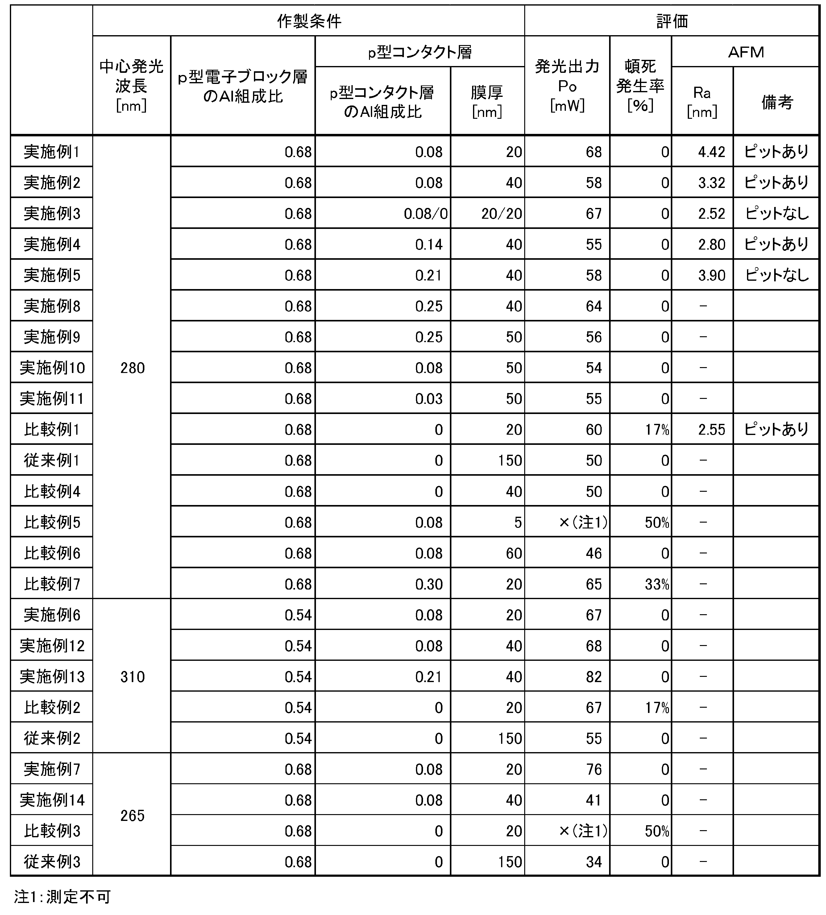
- Table 2 shows the results of the average value of the initial luminescence output and the incidence of death from death.
- the emission center wavelength of each sample was measured by an optical fiber spectroscope. The emission center wavelength is also shown in Table 2.
- the Al composition ratio of the p-type contact layer is within the range of 0.03 to 0.25. Further, it is understood that when the film thickness is in the range of 10 to 50 nm, it is possible to obtain a light emitting element having a larger light emission output than the conventional one without causing death. And it turns out that the result is the same also in Example 6, 12, 13 of wavelength 310nm, and Example 7, 14 of wavelength 265nm.
- substrate 20 buffer layer 30 n-type semiconductor layer 40 light emitting layer 41 well layer 42 barrier layer 60 p-type AlGaN electron block layer 70 p-type contact layer 71 p-type AlGaN contact layer 72 p-type GaN layer 80 p-side reflective electrode 90 n-side Electrode 100 Group III nitride semiconductor light emitting device
Landscapes
- Led Devices (AREA)
Abstract
Description
前記発光層からの発光の発光中心波長が250nm以上330nm以下であり、
前記p型AlGaN電子ブロック層のAl組成比は0.40以上0.80以下であり、
前記p型コンタクト層の膜厚は10nm以上50nm以下であり、かつ、該p型コンタクト層は、Al組成比が0.03以上0.25以下であるp型AlGaNコンタクト層を有することを特徴とするIII族窒化物半導体発光素子。
前記n型半導体層上に発光層を形成する工程と、
前記発光層上にp型AlGaN電子ブロック層を形成する工程と、
前記p型AlGaN電子ブロック層上にp型コンタクト層を形成する工程と、
前記p型コンタクト層上にp側反射電極を形成する工程と、を含むIII族窒化物半導体発光素子の製造方法であって、
前記発光層からの発光中心波長は250nm以上330nm以下であり、
前記p型AlGaN電子ブロック層のAl組成比は0.40以上0.80以下であり、
前記p型コンタクト層の膜厚が10nm以上50nm以下であり、
前記p型コンタクト層はAl組成比が0.03以上0.25以下であるp型AlGaNコンタクト層を形成することを特徴とするIII族窒化物半導体発光素子の製造方法。
本発明の一実施形態に従うIII族窒化物半導体発光素子100は、図1に示すように、基板10上に、n型半導体層30、発光層40、p型AlGaN電子ブロック層60、p型コンタクト層70及びp側反射電極80を順次備える。そして、発光層40からの発光の発光中心波長が250nm以上330nm以下であり、p型AlGaN電子ブロック層60のAl組成比は0.40以上0.80以下であり、p型コンタクト層70の膜厚は10nm以上50nm以下であり、かつ、p型コンタクト層70はAl組成比が0.03以上0.25以下であるp型AlGaNコンタクト層71を有する。
III族窒化物半導体発光素子100の基板10として、サファイア基板を用いることができる。サファイア基板の表面にエピタキシャル成長させたAlN層が設けられたAlNテンプレート基板を用いてもよい。サファイア基板としては、任意のサファイア基板を用いることができ、オフ角の有無は任意であり、オフ角が設けられている場合の傾斜方向の結晶軸方位は、m軸方向またはa軸方向のいずれでもよい。例えば、サファイア基板の主面を、C面が0.5度のオフ角θで傾斜した面とすることができる。AlNテンプレート基板を用いる場合、サファイア基板表面のAlN層の結晶性が優れていることが好ましい。また、AlNテンプレート基板の表面に、アンドープのAlGaN層が設けられていることも好ましい。また、基板10としてAlN単結晶基板を用いてもよい。
n型半導体層30は必要によりバッファ層20を介して基板10上に設けられる。n型半導体層30を基板10上に直接設けてもよい。n型半導体層30には、n型のドーパントがドープされたAlGaNを用いることができる。必要に応じて、In等のIII族元素を5%以内の組成比で導入し、AlGaInN等としてもよい。n型ドーパントの具体例として、シリコン(Si),ゲルマニウム(Ge),錫(Sn),硫黄(S),酸素(O),チタン(Ti),ジルコニウム(Zr)等を挙げることができる。n型ドーパントのドーパント濃度は、n型半導体層30がn型として機能することのできるドーパント濃度であれば特に限定されず、例えば1.0×10¹⁸atoms/cm3~1.0×1020atoms/cm3とすることができる。また、n型半導体層30のバンドギャップは、発光層40(量子井戸構造とする場合は井戸層41)のバンドギャップよりも広く、発光する深紫外光に対し透過性を有することが好ましい。また、n型半導体層30を単層構造や複数層からなる構造の他、III族元素の組成比を結晶成長方向に組成傾斜させた組成傾斜層や超格子構造を含む構成することもできる。n型半導体層30は、n側電極90とのコンタクト部を形成するだけでなく、基板から発光層に至るまでに結晶性を高める機能を兼ねることもできる。
発光層40はn型半導体層30上に設けられ、発光中心波長が250nm以上330nm以下の深紫外光を放射する。発光層40は、AlGaNとすることができ、そのAl組成比は所望の発光中心波長が得られるよう適宜設定すればよく、例えば0.17~0.70の範囲内とすることができる。
p型AlGaN電子ブロック層60は発光層40上に設けられる。p型AlGaN電子ブロック層60は電子を堰止めし、電子を発光層40(MQW構造の場合には井戸層41)内に注入して、電子の注入効率を高めるための層として用いられる。本発明においては、p型AlGaN電子ブロック層として、そのAl組成比を0.40以上0.80以下とするp型のAlzGa1-zN(0.40≦z≦0.80)を用いることができる。必要に応じて、In等のIII族元素を5%以内の組成比で導入した四元系のAlGaInN材料等としてもよいが、III族元素としてはAlおよびGaのみを用いた三元系のAlGaN材料とすることがより好ましい。Al組成比がこの範囲であるとp型AlGaN電子ブロック層60に転位が比較的多く形成されるため、このような場合に本発明によるp型コンタクト層70を用いることが有効となる。Al組成比が0.60以上0.70以下の場合に特に転位が形成されやすい。
p型コンタクト層70はp型AlGaN電子ブロック層60上に直接設けられる。p型コンタクト層70は、その最表面上に設けられるp側反射電極80と、p型AlGaN電子ブロック層60との間の接触抵抗を低減するための層である。本発明においては、p型コンタクト層70の膜厚を10nm以上50nm以下とする。そして、p型コンタクト層70はAl組成比xを0.03以上0.25以下とするp型AlGaN層71を有する。そして、p型AlGaNコンタクト層71はp型AlGaN電子ブロック層60の直上に接して形成され、組成式AlxGa1-xNのAl組成比xが0.03≦x≦0.25を用いることができる。p型コンタクト層70がp型AlGaN電子ブロック層60の直上にp型AlGaN層71を有することにより、III族窒化物半導体発光素子100の頓死を防止できることが本発明者の実験によって確認された。p型GaN層をp型AlGaN電子ブロック層60の直上に形成することに代えて、p型AlGaNコンタクト層71(AlxGa1-xN、0.03≦x≦0.25)を形成した方が、表面平坦性の悪化の悪影響を押さえつつ、成長初期に形成される転位の発生を抑えられるからだと考えられる。
p側反射電極80を、p型コンタクト層70の直上(最表面上)に設けることができる。p側反射電極80は、発光層40から放射される紫外光に対して高い反射率(例えば60%以上)を有する金属を用いることが好ましい。このような反射率を有する金属として、例えば、ロジウム(Rh)、白金(Pt)、イリジウム(Ir)、ルテニウム(Ru)、モリブデン(Mo)、タングステン(W)、タンタル(Ta)、及びこれらのいずれかを少なくとも含有する合金を挙げるができる。これらの金属又は合金は、深紫外光への反射率が高く、また、p型コンタクト層70と、p側反射電極80とで比較的良好なオーミック接触を取ることもできるため好ましい。なお、反射率の観点では、これらの中でも、p側反射電極80がロジウム(Rh)を単体又は合金の形態で含むことが好ましい。また、p側反射電極80の膜厚、形状及びサイズは、III族窒化物半導体発光素子100の形状及びサイズに応じて適宜選択することができ、例えばp側反射電極80の膜厚を30~45nmとすることができる。
図1に示すように、基板10と、n型半導体層30との間に、両者の格子不整合を緩和するためのバッファ層20を設けることも好ましい。バッファ層20としてアンドープのIII族窒化物半導体層を用いることができ、例えばアンドープのAlNを用いることができる。バッファ層20を超格子構造としてもよい。バッファ層20とn型半導体層30の間には、AlGaN層、組成傾斜層および超格子層の1つ以上から選ばれるバッファ層がさらに設けられてもよい。
n型半導体層30の露出面上に設けられ得るn側電極90は、例えばTi含有膜及びこのTi含有膜上に形成されたAl含有膜を有する金属複合膜とすることができる。n側電極90の膜厚、形状及びサイズは、発光素子の形状及びサイズに応じて適宜選択することができる。n側電極90は、図1に示すような、n型半導体層30の露出面上への形成に限定されず、n型半導体層と電気的に接続していればよい。
なお、図1には図示しないが、発光層40と、p型AlGaN電子ブロック層60との間に、p型AlGaN電子ブロック層60のAl組成比よりもAl組成比の高いAlGaN又はAlNからなるp型のガイド層を設けてもよい。ガイド層を設けることで、発光層40への正孔の注入を促進することができる。
さらに、図1には図示しないものの、発光層40とn型半導体層30との間に、n型ガイド層を設けてもよい。n型ガイド層はAlGaNを用いることが好ましく、そのAl組成比は、前記のn型半導体層30のAl組成比以上、かつ、障壁層42のAl組成比b以下とすることが好ましい。その膜厚は3nm~30nmとすることができる。また、n型ガイド層には、n型半導体層30と同様にn型のドーパント(不純物)がドープされことが好ましいが、そのドーパント量はn型層よりも低いことが好ましい。
次に、上述したIII族窒化物半導体発光素子100の製造方法の一実施形態を、図3を参照して説明する。本発明に従うIII族窒化物半導体発光素子100の製造方法の一実施形態は、基板10上に(ステップA参照)、n型半導体層30を形成する工程と、n型半導体層30上に発光層40を形成する工程と、発光層40上にp型AlGaN電子ブロック層60を形成する工程(ステップB参照)と、p型AlGaN電子ブロック層60上にp型コンタクト層70を形成する工程(ステップC参照)と、p型コンタクト層70上にp側反射電極80を形成する工程(ステップD参照)、とを含む。ここで、本製造方法の一実施形態では、発光層40からの発光の発光中心波長は250nm以上330nm以下であり、p型AlGaN電子ブロック層60のAl組成比は0.40以上0.80以下であり、p型コンタクト層70の膜厚が10nm以上50nm以下である。また、p型コンタクト層70はAl組成比が0.03以上0.25以下であるp型AlGaNコンタクト層71を形成する。
サファイア基板(直径2インチ、膜厚:430μm、面方位:(0001)、m軸方向オフ角θ:0.5度)を用意した。次いで、MOCVD法により、上記サファイア基板上に中心膜厚0.60μm(平均膜厚0.61μm)のAlN層を成長させ、AlNテンプレート基板とした。その際、AlN層の成長温度は1300℃、チャンバ内の成長圧力は10Torrであり、V/III比が163となるようにアンモニアガスとTMAガスの成長ガス流量を設定した。V族元素ガス(NH3)の流量は200sccm、III族元素ガス(TMA)の流量は53sccmである。なお、AlN層の膜厚については、光干渉式膜厚測定機(ナノスペックM6100A;ナノメトリックス社製)を用いて、ウェーハ面内の中心を含む、等間隔に分散させた計25箇所の膜厚を測定した。
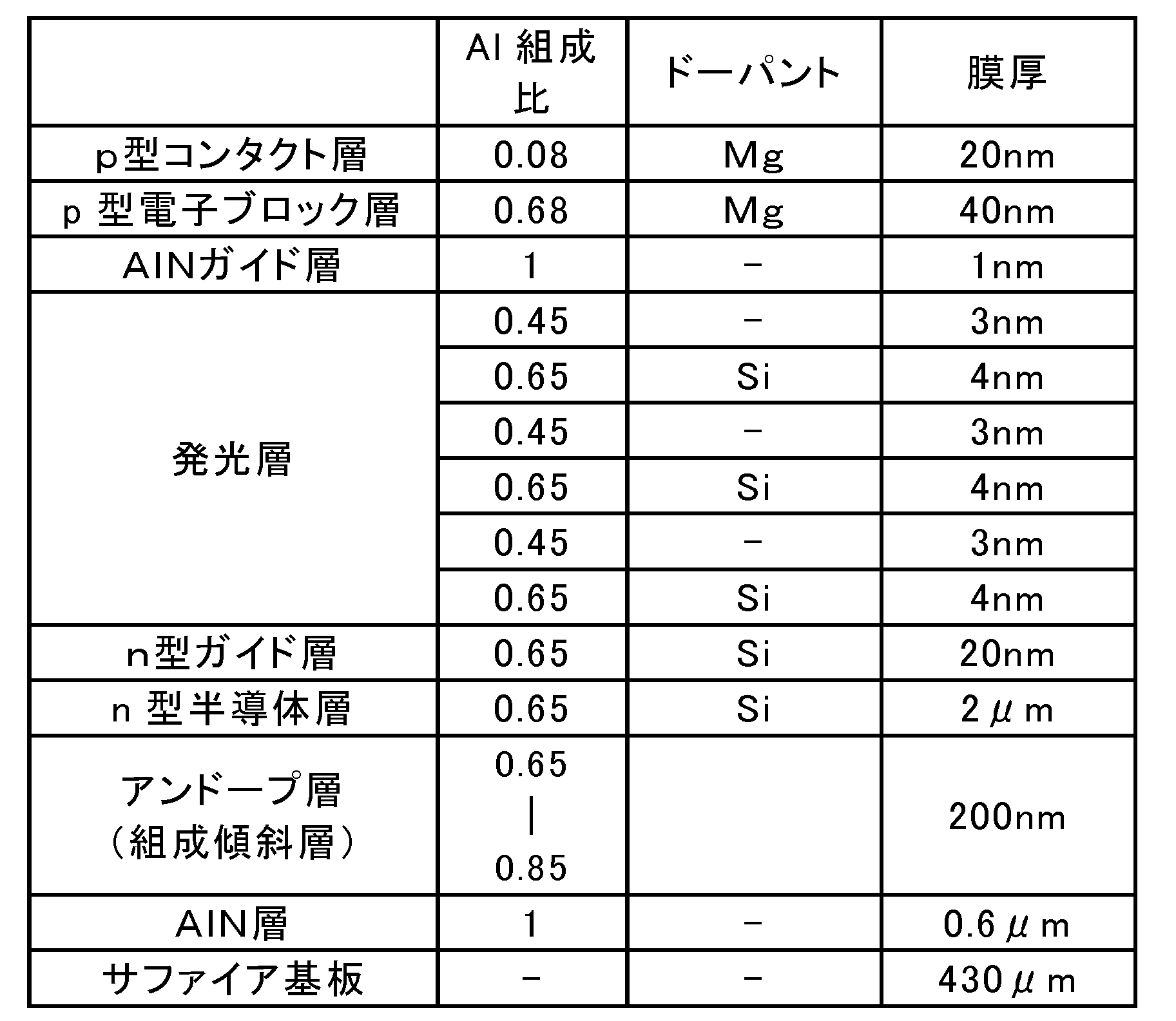
実施例1におけるp型コンタクト層の膜厚及びAl組成比を表2に記載のとおりに変えた以外は、実施例1と同様にして、実施例2~5,比較例1、従来例1に係るIII族窒化物半導体発光素子を作製した。なお、実施例3においては、p型Al0.68Ga0.32N電子ブロック層上に膜厚20nmのp型Al0.08Ga0.92Nコンタクト層を形成し、次いで膜厚20nmのp型GaNコンタクト層を形成した。さらに、実施例1におけるp型コンタクト層の膜厚及びAl組成比を表2に記載のとおりに変えた以外は、実施例1と同様にして、実施例8~11、比較例4~7に係るIII族窒化物半導体発光素子を作製した。
実施例1における井戸層のAl組成比w:0.45のAl組成比を0.30に変え、さらにアンドープ層のAl組成比を0.55、n型半導体層のAl組成比を0.45、nガイド層及び障壁層のAl組成比を0.55、p型電子ブロック層のAl組成比を0.58に変えつつ、p型コンタクト層の膜厚及びAl組成比xを表2に記載のとおりに変えた以外は、実施例1と同様にして、実施例6、比較例2、従来例2に係るIII族窒化物半導体発光素子を作製した。さらに、実施例6におけるp型コンタクト層の膜厚及びAl組成比を表2に記載のとおりに変えた以外は、実施例6と同様にして、実施例12および13に係るIII族窒化物半導体発光素子を作製した。
実施例1における井戸層のAl組成比w:0.45のAl組成比を0.58に変え、さらに障壁層のAl組成比を0.76に変え、p型コンタクト層の膜厚及びAl組成比xを表2に記載のとおりに変えた以外は、実施例1と同様にして、実施例7、比較例3、従来例3に係るIII族窒化物半導体発光素子を作製した。さらに、実施例7におけるp型コンタクト層の膜厚及びAl組成比を表2に記載のとおりに変えた以外は、実施例7と同様にして、実施例14に係るIII族窒化物半導体発光素子を作製した。
実施例1~7、8~14、比較例1~3、4~7、従来例1~3のそれぞれに対し、エピタキシャル成長により形成される各層の膜厚は、光干渉式膜厚測定器を用いて測定した。また、障壁層や電子ブロック層を含め各層の膜厚が数nm~数十nmと薄い層は、透過型電子顕微鏡による各層の断面観察でのTEM-EDSを用いて各層膜厚とAl組成比を測定した。なお、各層の膜厚の測定位置はウェーハ中央部である。
実施例1~7、8~14、比較例1~3、4~7、従来例1~3から得られた発光素子(測定個数24個)に対して、定電流電圧電源を用いて電流20mAにて通電し、発光出力を測り、次いで100mAで3秒間通電した後、再び20mAで通電して発光出力を測り、初期の発光出力に対する発光出力の変化を測定した。このとき、通電により発光する面積は0.057mm2であった。100mAで3秒間通電した後の発光出力が初期の発光出力の半分以下にまで下がったもの、すなわち頓死が発生する発光素子の個数を確認した。実施例1~7及び従来例1~3では電流100mAでの通電後も大きな変化はなかったが、比較例1~3では、電流100mAでの通電後に、ウェーハ内で不点灯、あるいは初期の発光出力から半減以下の出力となる発光素子が確認された(すなわち、頓死の発生が確認された)。こうした不点灯や、初期の発光出力の半分以下への発光出力の急減がなかったものの比率を、頓死発生率として表2に示す。なお、発光出力Poの測定にあたっては積分球を用いた。初期の発光出力の平均値と頓死の発生率の結果を表2に示す。なお、光ファイバ分光器によって各サンプルの発光中心波長を測定した。発光中心波長についても表2に示す。
代表例として、実施例1~5、比較例1のp型コンタクト層の最表面について、原子間力顕微鏡(AFM: Atomic Force Microscope)によりAFM像を取得しつつ、表面粗さの指標としてRa(平均粗さ;JIS B 0601:2001に準拠)を測定した。なお、測定箇所はウェーハ中央部である。Raの測定値を表2に示す。なお、実施例1~5、比較例1については、基板観察によるピットの有無も併せて示す。さらに、実施例1~3、比較例1によるAFM像を図4A~図4Dにそれぞれ示す。
本発明条件に従う実施例1~7では、同波長で比較した場合に、信頼性を確保したまま、従来例1~3のそれぞれよりも発光出力を増大させることができた。比較例1,2ではp型コンタクト層を薄くしたために発光層からの光吸収を抑制できる結果、発光出力を増大させることはできたものの、頓死の発生が確認された。比較例3では、初期通電から頓死が多発し、発光出力を測定することすらできなかった。
20 バッファ層
30 n型半導体層
40 発光層
41 井戸層
42 障壁層
60 p型AlGaN電子ブロック層
70 p型コンタクト層
71 p型AlGaNコンタクト層
72 p型GaN層
80 p側反射電極
90 n側電極
100 III族窒化物半導体発光素子
Claims (5)
- 基板上に、n型半導体層、発光層、p型AlGaN電子ブロック層、p型コンタクト層及びp側反射電極を順次備えるIII族窒化物半導体発光素子であって、
前記発光層からの発光の発光中心波長が250nm以上330nm以下であり、
前記p型AlGaN電子ブロック層のAl組成比は0.40以上0.80以下であり、
前記p型コンタクト層の膜厚は10nm以上50nm以下であり、かつ、該p型コンタクト層は、Al組成比が0.03以上0.25以下であるp型AlGaNコンタクト層を有することを特徴とするIII族窒化物半導体発光素子。 - 前記p型コンタクト層は、前記p型AlGaNコンタクト層のみからなる、請求項1に記載のIII族窒化物半導体発光素子。
- 前記p型コンタクト層は、前記p型AlGaNコンタクト層と前記p側反射電極との間にp型GaNコンタクト層を有する、請求項1に記載のIII族窒化物半導体発光素子。
- 前記p型AlGaNコンタクト層の膜厚が10nm以上25nm以下である、請求項1~3のいずれか1項に記載のIII族窒化物半導体発光素子。
- 基板上に、n型半導体層を形成する工程と、
前記n型半導体層上に発光層を形成する工程と、
前記発光層上にp型AlGaN電子ブロック層を形成する工程と、
前記p型AlGaN電子ブロック層上にp型コンタクト層を形成する工程と、
前記p型コンタクト層上にp側反射電極を形成する工程と、を含むIII族窒化物半導体発光素子の製造方法であって、
前記発光層からの発光中心波長は250nm以上330nm以下であり、
前記p型AlGaN電子ブロック層のAl組成比は0.40以上0.80以下であり、
前記p型コンタクト層の膜厚が10nm以上50nm以下であり、
前記p型コンタクト層はAl組成比が0.03以上0.25以下であるp型AlGaNコンタクト層を有すること特徴とするIII族窒化物半導体発光素子の製造方法。
Priority Applications (2)
| Application Number | Priority Date | Filing Date | Title |
|---|---|---|---|
| US17/312,934 US12268038B2 (en) | 2018-12-14 | 2019-12-11 | Group III nitride semiconductor light emitting element and method of manufacturing the same |
| CN201980082293.3A CN113169255B (zh) | 2018-12-14 | 2019-12-11 | Iii族氮化物半导体发光元件及其制造方法 |
Applications Claiming Priority (4)
| Application Number | Priority Date | Filing Date | Title |
|---|---|---|---|
| JP2018234216 | 2018-12-14 | ||
| JP2018-234216 | 2018-12-14 | ||
| JP2019223516A JP6753995B2 (ja) | 2018-12-14 | 2019-12-11 | Iii族窒化物半導体発光素子及びその製造方法 |
| JP2019-223516 | 2019-12-11 |
Publications (1)
| Publication Number | Publication Date |
|---|---|
| WO2020122137A1 true WO2020122137A1 (ja) | 2020-06-18 |
Family
ID=71076470
Family Applications (1)
| Application Number | Title | Priority Date | Filing Date |
|---|---|---|---|
| PCT/JP2019/048537 Ceased WO2020122137A1 (ja) | 2018-12-14 | 2019-12-11 | Iii族窒化物半導体発光素子及びその製造方法 |
Country Status (2)
| Country | Link |
|---|---|
| US (1) | US12268038B2 (ja) |
| WO (1) | WO2020122137A1 (ja) |
Cited By (2)
| Publication number | Priority date | Publication date | Assignee | Title |
|---|---|---|---|---|
| JPWO2022202342A1 (ja) * | 2021-03-23 | 2022-09-29 | ||
| JP2023039354A (ja) * | 2021-09-08 | 2023-03-20 | 日亜化学工業株式会社 | 発光素子 |
Citations (5)
| Publication number | Priority date | Publication date | Assignee | Title |
|---|---|---|---|---|
| CN101604716A (zh) * | 2008-06-10 | 2009-12-16 | 北京大学 | 一种深紫外发光二极管及其制备方法 |
| US20140103289A1 (en) * | 2010-04-30 | 2014-04-17 | Yitao Liao | High efficiency ultraviolet light emitting diode with band structure potential fluctuations |
| JP2016088803A (ja) * | 2014-11-04 | 2016-05-23 | Dowaエレクトロニクス株式会社 | Iii族窒化物半導体エピタキシャル基板およびその製造方法、ならびにiii族窒化物半導体発光素子 |
| WO2017017891A1 (ja) * | 2015-07-30 | 2017-02-02 | Dowaエレクトロニクス株式会社 | Iii族窒化物半導体発光素子およびその製造方法 |
| WO2018181044A1 (ja) * | 2017-03-27 | 2018-10-04 | Dowaエレクトロニクス株式会社 | Iii族窒化物半導体発光素子およびその製造方法 |
Family Cites Families (11)
| Publication number | Priority date | Publication date | Assignee | Title |
|---|---|---|---|---|
| JP4653671B2 (ja) * | 2005-03-14 | 2011-03-16 | 株式会社東芝 | 発光装置 |
| US20060267043A1 (en) * | 2005-05-27 | 2006-11-30 | Emerson David T | Deep ultraviolet light emitting devices and methods of fabricating deep ultraviolet light emitting devices |
| JP5401145B2 (ja) | 2009-03-26 | 2014-01-29 | 株式会社トクヤマ | Iii族窒化物積層体の製造方法 |
| JP6001627B2 (ja) * | 2014-12-08 | 2016-10-05 | Dowaエレクトロニクス株式会社 | Iii族窒化物半導体発光素子の製造方法 |
| JP5953447B1 (ja) | 2015-02-05 | 2016-07-20 | Dowaエレクトロニクス株式会社 | Iii族窒化物半導体発光素子およびその製造方法 |
| JP2017050439A (ja) | 2015-09-03 | 2017-03-09 | 豊田合成株式会社 | 紫外発光素子およびその製造方法 |
| US10340416B2 (en) * | 2016-02-26 | 2019-07-02 | Riken | Crystal substrate, ultraviolet light-emitting device, and manufacturing methods therefor |
| JP6908422B2 (ja) | 2016-04-20 | 2021-07-28 | Dowaエレクトロニクス株式会社 | Iii族窒化物半導体発光素子およびその製造方法 |
| US10290771B2 (en) * | 2016-04-20 | 2019-05-14 | Dowa Electronics Materials Co., Ltd. | Group III nitride semiconductor light emitting device and method for manufacture the same |
| JP6431013B2 (ja) | 2016-09-21 | 2018-11-28 | シャープ株式会社 | 窒化アルミニウム系半導体深紫外発光素子 |
| JP6654596B2 (ja) * | 2017-03-24 | 2020-02-26 | 日機装株式会社 | 半導体発光素子および半導体発光素子の製造方法 |
-
2019
- 2019-12-11 WO PCT/JP2019/048537 patent/WO2020122137A1/ja not_active Ceased
- 2019-12-11 US US17/312,934 patent/US12268038B2/en active Active
Patent Citations (5)
| Publication number | Priority date | Publication date | Assignee | Title |
|---|---|---|---|---|
| CN101604716A (zh) * | 2008-06-10 | 2009-12-16 | 北京大学 | 一种深紫外发光二极管及其制备方法 |
| US20140103289A1 (en) * | 2010-04-30 | 2014-04-17 | Yitao Liao | High efficiency ultraviolet light emitting diode with band structure potential fluctuations |
| JP2016088803A (ja) * | 2014-11-04 | 2016-05-23 | Dowaエレクトロニクス株式会社 | Iii族窒化物半導体エピタキシャル基板およびその製造方法、ならびにiii族窒化物半導体発光素子 |
| WO2017017891A1 (ja) * | 2015-07-30 | 2017-02-02 | Dowaエレクトロニクス株式会社 | Iii族窒化物半導体発光素子およびその製造方法 |
| WO2018181044A1 (ja) * | 2017-03-27 | 2018-10-04 | Dowaエレクトロニクス株式会社 | Iii族窒化物半導体発光素子およびその製造方法 |
Cited By (4)
| Publication number | Priority date | Publication date | Assignee | Title |
|---|---|---|---|---|
| JPWO2022202342A1 (ja) * | 2021-03-23 | 2022-09-29 | ||
| WO2022202342A1 (ja) * | 2021-03-23 | 2022-09-29 | 旭化成株式会社 | 紫外線発光素子 |
| JP2023039354A (ja) * | 2021-09-08 | 2023-03-20 | 日亜化学工業株式会社 | 発光素子 |
| US12527126B2 (en) | 2021-09-08 | 2026-01-13 | Nichia Corporation | Light-emitting element including p-side semiconductor layer having first, second, and third layers |
Also Published As
| Publication number | Publication date |
|---|---|
| US12268038B2 (en) | 2025-04-01 |
| US20220045239A1 (en) | 2022-02-10 |
Similar Documents
| Publication | Publication Date | Title |
|---|---|---|
| CN110462851B (zh) | Iii族氮化物半导体发光元件及其制造方法 | |
| CN113169255B (zh) | Iii族氮化物半导体发光元件及其制造方法 | |
| CN111164768B (zh) | 深紫外发光元件及其制造方法 | |
| CN107851689B (zh) | Ⅲ族氮化物半导体发光元件及其制造方法 | |
| US9882088B2 (en) | III nitride semiconductor light-emitting device | |
| US11804567B2 (en) | III-nitride semiconductor light-emitting device and method of producing the same | |
| JP6766243B2 (ja) | Iii族窒化物半導体発光素子およびその製造方法 | |
| US11984535B2 (en) | III-nitride semiconductor light-emitting device comprising barrier layers and well layers and method of producing the same | |
| US12268038B2 (en) | Group III nitride semiconductor light emitting element and method of manufacturing the same | |
| TWI722784B (zh) | 深紫外發光元件用的反射電極的製造方法、深紫外發光元件的製造方法及深紫外發光元件 | |
| WO2020153308A1 (ja) | 深紫外発光素子用の反射電極の製造方法、深紫外発光素子の製造方法および深紫外発光素子 |
Legal Events
| Date | Code | Title | Description |
|---|---|---|---|
| 121 | Ep: the epo has been informed by wipo that ep was designated in this application |
Ref document number: 19894982 Country of ref document: EP Kind code of ref document: A1 |
|
| NENP | Non-entry into the national phase |
Ref country code: DE |
|
| 122 | Ep: pct application non-entry in european phase |
Ref document number: 19894982 Country of ref document: EP Kind code of ref document: A1 |
|
| WWG | Wipo information: grant in national office |
Ref document number: 17312934 Country of ref document: US |
|
| WWG | Wipo information: grant in national office |
Ref document number: 201980082293.3 Country of ref document: CN |