WO2020121961A1 - 回路基板及び車両用灯具 - Google Patents
回路基板及び車両用灯具 Download PDFInfo
- Publication number
- WO2020121961A1 WO2020121961A1 PCT/JP2019/047793 JP2019047793W WO2020121961A1 WO 2020121961 A1 WO2020121961 A1 WO 2020121961A1 JP 2019047793 W JP2019047793 W JP 2019047793W WO 2020121961 A1 WO2020121961 A1 WO 2020121961A1
- Authority
- WO
- WIPO (PCT)
- Prior art keywords
- circuit board
- region
- board
- wiring
- area
- Prior art date
- Legal status (The legal status is an assumption and is not a legal conclusion. Google has not performed a legal analysis and makes no representation as to the accuracy of the status listed.)
- Ceased
Links
Images


Classifications
-
- F—MECHANICAL ENGINEERING; LIGHTING; HEATING; WEAPONS; BLASTING
- F21—LIGHTING
- F21S—NON-PORTABLE LIGHTING DEVICES; SYSTEMS THEREOF; VEHICLE LIGHTING DEVICES SPECIALLY ADAPTED FOR VEHICLE EXTERIORS
- F21S41/00—Illuminating devices specially adapted for vehicle exteriors, e.g. headlamps
- F21S41/10—Illuminating devices specially adapted for vehicle exteriors, e.g. headlamps characterised by the light source
- F21S41/14—Illuminating devices specially adapted for vehicle exteriors, e.g. headlamps characterised by the light source characterised by the type of light source
- F21S41/141—Light emitting diodes [LED]
- F21S41/147—Light emitting diodes [LED] the main emission direction of the LED being angled to the optical axis of the illuminating device
-
- F—MECHANICAL ENGINEERING; LIGHTING; HEATING; WEAPONS; BLASTING
- F21—LIGHTING
- F21S—NON-PORTABLE LIGHTING DEVICES; SYSTEMS THEREOF; VEHICLE LIGHTING DEVICES SPECIALLY ADAPTED FOR VEHICLE EXTERIORS
- F21S41/00—Illuminating devices specially adapted for vehicle exteriors, e.g. headlamps
- F21S41/10—Illuminating devices specially adapted for vehicle exteriors, e.g. headlamps characterised by the light source
- F21S41/19—Attachment of light sources or lamp holders
-
- F—MECHANICAL ENGINEERING; LIGHTING; HEATING; WEAPONS; BLASTING
- F21—LIGHTING
- F21S—NON-PORTABLE LIGHTING DEVICES; SYSTEMS THEREOF; VEHICLE LIGHTING DEVICES SPECIALLY ADAPTED FOR VEHICLE EXTERIORS
- F21S41/00—Illuminating devices specially adapted for vehicle exteriors, e.g. headlamps
- F21S41/30—Illuminating devices specially adapted for vehicle exteriors, e.g. headlamps characterised by reflectors
- F21S41/32—Optical layout thereof
- F21S41/36—Combinations of two or more separate reflectors
-
- F—MECHANICAL ENGINEERING; LIGHTING; HEATING; WEAPONS; BLASTING
- F21—LIGHTING
- F21S—NON-PORTABLE LIGHTING DEVICES; SYSTEMS THEREOF; VEHICLE LIGHTING DEVICES SPECIALLY ADAPTED FOR VEHICLE EXTERIORS
- F21S41/00—Illuminating devices specially adapted for vehicle exteriors, e.g. headlamps
- F21S41/60—Illuminating devices specially adapted for vehicle exteriors, e.g. headlamps characterised by a variable light distribution
- F21S41/65—Illuminating devices specially adapted for vehicle exteriors, e.g. headlamps characterised by a variable light distribution by acting on light sources
- F21S41/663—Illuminating devices specially adapted for vehicle exteriors, e.g. headlamps characterised by a variable light distribution by acting on light sources by switching light sources
-
- F—MECHANICAL ENGINEERING; LIGHTING; HEATING; WEAPONS; BLASTING
- F21—LIGHTING
- F21S—NON-PORTABLE LIGHTING DEVICES; SYSTEMS THEREOF; VEHICLE LIGHTING DEVICES SPECIALLY ADAPTED FOR VEHICLE EXTERIORS
- F21S45/00—Arrangements within vehicle lighting devices specially adapted for vehicle exteriors, for purposes other than emission or distribution of light
- F21S45/40—Cooling of lighting devices
- F21S45/42—Forced cooling
- F21S45/43—Forced cooling using gas
-
- F—MECHANICAL ENGINEERING; LIGHTING; HEATING; WEAPONS; BLASTING
- F21—LIGHTING
- F21S—NON-PORTABLE LIGHTING DEVICES; SYSTEMS THEREOF; VEHICLE LIGHTING DEVICES SPECIALLY ADAPTED FOR VEHICLE EXTERIORS
- F21S45/00—Arrangements within vehicle lighting devices specially adapted for vehicle exteriors, for purposes other than emission or distribution of light
- F21S45/40—Cooling of lighting devices
- F21S45/47—Passive cooling, e.g. using fins, thermal conductive elements or openings
-
- F—MECHANICAL ENGINEERING; LIGHTING; HEATING; WEAPONS; BLASTING
- F21—LIGHTING
- F21S—NON-PORTABLE LIGHTING DEVICES; SYSTEMS THEREOF; VEHICLE LIGHTING DEVICES SPECIALLY ADAPTED FOR VEHICLE EXTERIORS
- F21S45/00—Arrangements within vehicle lighting devices specially adapted for vehicle exteriors, for purposes other than emission or distribution of light
- F21S45/70—Prevention of harmful light leakage
-
- F—MECHANICAL ENGINEERING; LIGHTING; HEATING; WEAPONS; BLASTING
- F21—LIGHTING
- F21V—FUNCTIONAL FEATURES OR DETAILS OF LIGHTING DEVICES OR SYSTEMS THEREOF; STRUCTURAL COMBINATIONS OF LIGHTING DEVICES WITH OTHER ARTICLES, NOT OTHERWISE PROVIDED FOR
- F21V19/00—Fastening of light sources or lamp holders
-
- F—MECHANICAL ENGINEERING; LIGHTING; HEATING; WEAPONS; BLASTING
- F21—LIGHTING
- F21V—FUNCTIONAL FEATURES OR DETAILS OF LIGHTING DEVICES OR SYSTEMS THEREOF; STRUCTURAL COMBINATIONS OF LIGHTING DEVICES WITH OTHER ARTICLES, NOT OTHERWISE PROVIDED FOR
- F21V29/00—Protecting lighting devices from thermal damage; Cooling or heating arrangements specially adapted for lighting devices or systems
- F21V29/50—Cooling arrangements
- F21V29/502—Cooling arrangements characterised by the adaptation for cooling of specific components
- F21V29/503—Cooling arrangements characterised by the adaptation for cooling of specific components of light sources
-
- F—MECHANICAL ENGINEERING; LIGHTING; HEATING; WEAPONS; BLASTING
- F21—LIGHTING
- F21V—FUNCTIONAL FEATURES OR DETAILS OF LIGHTING DEVICES OR SYSTEMS THEREOF; STRUCTURAL COMBINATIONS OF LIGHTING DEVICES WITH OTHER ARTICLES, NOT OTHERWISE PROVIDED FOR
- F21V29/00—Protecting lighting devices from thermal damage; Cooling or heating arrangements specially adapted for lighting devices or systems
- F21V29/50—Cooling arrangements
- F21V29/60—Cooling arrangements characterised by the use of a forced flow of gas, e.g. air
- F21V29/67—Cooling arrangements characterised by the use of a forced flow of gas, e.g. air characterised by the arrangement of fans
-
- F—MECHANICAL ENGINEERING; LIGHTING; HEATING; WEAPONS; BLASTING
- F21—LIGHTING
- F21V—FUNCTIONAL FEATURES OR DETAILS OF LIGHTING DEVICES OR SYSTEMS THEREOF; STRUCTURAL COMBINATIONS OF LIGHTING DEVICES WITH OTHER ARTICLES, NOT OTHERWISE PROVIDED FOR
- F21V29/00—Protecting lighting devices from thermal damage; Cooling or heating arrangements specially adapted for lighting devices or systems
- F21V29/50—Cooling arrangements
- F21V29/70—Cooling arrangements characterised by passive heat-dissipating elements, e.g. heat-sinks
- F21V29/74—Cooling arrangements characterised by passive heat-dissipating elements, e.g. heat-sinks with fins or blades
- F21V29/76—Cooling arrangements characterised by passive heat-dissipating elements, e.g. heat-sinks with fins or blades with essentially identical parallel planar fins or blades, e.g. with comb-like cross-section
-
- H—ELECTRICITY
- H05—ELECTRIC TECHNIQUES NOT OTHERWISE PROVIDED FOR
- H05K—PRINTED CIRCUITS; CASINGS OR CONSTRUCTIONAL DETAILS OF ELECTRIC APPARATUS; MANUFACTURE OF ASSEMBLAGES OF ELECTRICAL COMPONENTS
- H05K1/00—Printed circuits
- H05K1/02—Details
Definitions
- the present invention relates to a circuit board and a vehicle lamp.
- a light emitting diode (LED: Light Emitting Diode) is widely used in the light emitting section.
- ADB Adaptive Driving Beam
- ADB Adaptive Driving Beam
- puts a plurality of LEDs in a one-dimensional or two-dimensional array and switches between turning on and off each LED according to the position of an oncoming vehicle or a preceding vehicle has been put into practical use.
- a marker lamp that performs a complicated display using an organic EL (Electro Luminescence) element in a light emitting portion (see, for example, Patent Document 1).
- a high-density printed wiring is formed on a substrate, and a flexible high-density flexible cable such as FPC (Flexible Printed Circuit) or FFC (Flexible Flat Cable) is used. It has been proposed to electrically connect the substrates (see, for example, Patent Document 1).
- the flexible cable can be attached and detached by inserting the flexible cable into the connector part mounted on the board.
- the flexible cable can be attached and detached by inserting the flexible cable into the connector part mounted on the board.
- a method of directly connecting the flexible cable to the terminal between the boards in the reflow process has also been proposed.
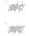
- FIG. 6 is a schematic view showing a connection between boards using a conventional flexible cable
- FIG. 6(a) shows two boards before connection
- FIG. 6(b) shows a state in which a flexible cable is connected. Shows.
- the wiring pattern 3 and the lands 4a and 4b are formed on the substrate 1 and the substrate 2, respectively.
- the flexible cable 5 is arranged between the lands 4a and 4b coated with the solder material and heated in the reflow process, the flexible cable 5 is connected between the lands 4a and 4b.
- the flexible cable 5 has flexibility, so that the substrate portions 12 are mounted on different planes. It is possible to
- the area of the lands 4a and 4b is essential, and it has been difficult to achieve further space saving.
- a solder material is used for connecting the flexible cable 5, it is difficult to ensure long-term reliability such as cracking when stress such as thermal shock is applied.
- the heat resistance of the adhesive affects the heat resistance of the flexible cable 5, and the environmental temperature of the post process is increased. There was also the problem of being restricted.
- the present invention has been made in view of the above conventional problems, and an object of the present invention is to provide a circuit board and a vehicular lamp that can secure long-term reliability while achieving space saving.
- a circuit board of the present invention has a first board portion, a second board portion formed separately from the first board portion, and has flexibility, and wiring on the surface.
- the first area and the second area of the wiring board are adhered to the first board section and the second board section, respectively, and the third area is provided between the first board section and the second board section. Since they are connected, lands and flexible cables are not required, and long-term reliability can be ensured while saving space.
- the first region has substantially the same shape as the first substrate portion.
- the adhesive layer is not formed on the back surface of the third region.
- the wiring board is made of glass epoxy resin.
- the wiring board has a thickness in the range of 0.1 mm to 0.3 mm.
- a vehicle lamp of the present invention includes the circuit board according to any one of the above, and a light emitting element mounted on the circuit board, wherein the first board portion and the second board portion include: It is characterized by being mounted on different planes.
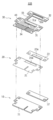
- FIG. 3 is an exploded perspective view schematically showing the structure of the circuit board 100.
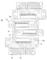
- FIG. 6 is a plan view schematically showing an arrangement example of the wiring board 30 when manufacturing the circuit board 100.
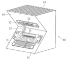
- FIG. 3 is a schematic perspective view showing a state where the circuit board 100 is mounted on the heat sink 60.
- FIG. 3 is a schematic cross-sectional view showing the structure of a vehicular lamp 200 using the circuit board 100.
- FIG.6(a) shows two boards before a connection
- FIG.6(b) has shown the state which connected the flexible cable.
- FIG. 1 is a schematic perspective view showing a circuit board 100 according to this embodiment.
- the circuit board 100 includes a first board portion 11, a second board portion 12, a wiring board 30, and a resist layer 40.
- the first substrate portion 11 and the second substrate portion 12 are substantially flat plate members made of a material having good thermal conductivity, and are formed separately.
- a wiring board 30 is bonded to one surface of each of the first board portion 11 and the second board portion 12, and a plurality of light emitting elements 51, 52 are mounted.
- the material forming the first substrate portion 11 and the second substrate portion 12 is not limited, it is preferable to use a metal having good thermal conductivity such as copper or aluminum.
- the wiring board 30 is a board having a wiring pattern 34 formed on the surface thereof and has flexibility.
- the wiring board 30 is adhered to the first board portion 11 and the second board portion 12 with an adhesive layer 20 described later. Further, the wiring board 30 is integrally formed with three regions, that is, a first region 31, a second region 32, and a third region 33, and a wiring pattern 34 is continuously formed over the three regions.
- the material forming the wiring board 30 is not limited, but it is preferable to use a glass epoxy resin because it has flexibility and mechanical strength.
- the thickness of the wiring board 30 is preferably in the range of 0.1 mm to 0.3 mm. If the thickness is larger than 0.3 mm, the flexibility is not sufficient and the bending radius becomes large, and if the thickness is smaller than 0.1 mm, the mechanical strength cannot be sufficiently secured and the handling becomes difficult.
- the first region 31 is a region formed in an outer shape corresponding to the first substrate portion 11, and the back surface side is bonded to the first substrate portion 11 with an adhesive layer 20 described later. Further, an opening 31a is formed in a predetermined area of the first area 31, and the surface of the first substrate portion 11 is exposed in the opening 31a.
- the second region 32 is a region formed in an outer shape corresponding to the second substrate portion 12, and the back surface side is bonded to the second substrate portion 12 with an adhesive layer 20 described later. Further, an opening 32a is formed in a predetermined area of the second area 32, and the surface of the second substrate portion 12 is exposed inside the opening 32a.
- the third area 33 is an area provided between the first area 31 and the second area 32. There is neither the first substrate portion 11 nor the second substrate portion 12 on the back surface side of the third region 33, and therefore, the adhesive layer 20 is not attached, and the first substrate portion 11 and the second substrate portion 12 are It has a structure that bridges the spaces.
- the wiring pattern 34 is a conductive pattern formed on the surface of the wiring board 30, and is for ensuring electrical connection between the respective regions in the circuit board 100. As shown in the figure, the wiring pattern 34 is continuously formed over three regions of the first region 31, the second region 32, and the third region 33, and the first substrate portion 11 and the second substrate portion 12 are formed. A single circuit is constructed between the and. A resist layer 40 is formed so as to cover the wiring pattern 34.
- the openings 31a and 32a are openings formed in the first region 31 and the second region 32, respectively.
- the surfaces of the first substrate portion 11 and the second substrate portion 12 are exposed from the openings 31a and 32a, respectively, and the light emitting elements 51 and 52 are mounted therein.
- the resist layer 40 is an insulating film-like member formed on the front surface side of the wiring board 30 so as to cover the wiring pattern 34.
- the resist layer 40 is formed in a region excluding a portion for bonding the light emitting elements 51 and 52 with a metal wire and a portion for electrically connecting from the outside.
- the material forming the resist layer 40 is not limited, but in order to suppress stray light due to the difference in light reflectance between the surface of the wiring board 30 and the wiring pattern 34, the light reflectance in the region where the resist layer 40 is formed is adjusted. It is preferable to use a light-reflecting material or a light-absorbing material so as to be uniform.
- the light emitting elements 51 and 52 are members that emit light when a voltage is applied, and are composed of a combination of an LED chip and a phosphor material. Although not shown in FIGS. 1 to 5, the light emitting elements 51 and 52 are electrically connected to the wiring patterns 34 in the first region 31 and the second region 32, respectively, using metal wires or the like.
- a known compound semiconductor material such as a GaN-based compound that emits blue, violet, or ultraviolet wavelengths as primary light can be used.
- the phosphor material a known material that is excited by primary light and emits desired secondary light can be used, and a material that obtains white color by mixing with the primary light from the LED chip or a plurality of phosphor materials can be used. It is possible to use one that obtains a white color by mixing a plurality of secondary lights.
- the first board portion 11 and the second board portion 12 are electrically and mechanically connected to each other by the third region 33 of the wiring board 30. Since the wiring substrate 30 is made of a flexible material, even if the first substrate portion 11 and the second substrate portion 12 are mounted on different surfaces, the third region 33 bends and electrical connection is made between them. Is maintained. Further, since it is not necessary to form the land for connecting the FPC with the solder on the circuit board 100, the space can be saved. When a glass epoxy resin is used as the wiring board 30, the heat resistance can be improved to 150° C. or higher. Further, the glass epoxy resin is more rigid than the conventional FPC, so that the handling in the mounting process becomes easy.
- FIG. 2 is an exploded perspective view schematically showing the structure of the circuit board 100.
- the circuit board 100 includes the heat dissipation portion 10 including the first substrate portion 11 and the second substrate portion 12, the adhesive layer 20 including the first adhesive sheet 21 and the second adhesive sheet 22, and the above-described.
- the wiring board 30 and the wiring board 30 are laminated.
- the adhesive layer 20 is a sheet-shaped adhesive material arranged between the front surface of the heat dissipation portion 10 and the back surface of the wiring board 30. As shown in FIG. 2, the adhesive layer 20 is separately formed into a first adhesive sheet 21 and a second adhesive sheet 22.
- the material forming the adhesive layer 20 is not particularly limited, but for example, a prepreg formed in a sheet shape with a thickness of 20 to 200 ⁇ m can be used.
- the first adhesive sheet 21 has a sheet shape formed in an outer shape corresponding to the first substrate portion 11, and the back surface side contacts the first substrate portion 11 and the front surface side contacts the first region 31. Further, the opening 21a is formed in a region and shape corresponding to the opening 31a.
- the second adhesive sheet 22 is a sheet formed in an outer shape corresponding to the second substrate portion 12, and the back surface side contacts the second substrate portion 12 and the front surface side contacts the second region 32. Further, the opening 22a is formed in a region and shape corresponding to the opening 32a.
- the heat dissipation part 10 and the adhesive layer 20 described above can be collectively formed into a plurality of outer shapes from a single plate-shaped member by punching or the like.
- the resist layer 40 is formed in a predetermined region on the wiring pattern 34, and the outer shape can be formed by punching. ..
- the heat dissipation portion 10 As a method of manufacturing the circuit board 100, the heat dissipation portion 10, the adhesive layer 20, and the wiring board 30 having a large size are stacked, and the wiring board 30 is adhered onto the heat dissipation portion 10 by applying heat and pressure in a lamination pressing process. A layered structure adhered with layer 20 is obtained.
- the outer shape of the circuit board 100 can be obtained by collectively punching the obtained laminated structure.
- the openings 21a, 31a, 22a, 32a may be formed before the laminating press working or may be formed by cutting after the laminating press working.
- the step of forming the wiring pattern 34 on the wiring board 30 may be performed before or after the lamination pressing step.
- the light emitting element 51 is mounted on the surface of the first substrate portion 11 exposed in the openings 21a and 31a, and the light emitting element 52 is mounted on the surface of the second substrate portion 12 exposed in the openings 22a and 32a.
- the light emitting elements 51 and 52 and the wiring pattern 34 are wire-bonded with a metal wire to obtain the circuit board 100 of the present invention.
- FIG. 3 is a plan view schematically showing an arrangement example of the wiring board 30 when manufacturing the circuit board 100.
- the two circuit boards 100 are rotated 180 degrees with respect to each other on one glass epoxy resin sheet so that the other first area 31 is located next to one third area 33.
- FIG. 4 is a schematic perspective view showing a state in which the circuit board 100 is mounted on the heat sink 60.
- the heat sink 60 is a member having good thermal conductivity, which is arranged in contact with the back surface of the circuit board 100, and may be made of aluminum or the like.
- a first surface 61 and a second surface 62 are formed in front of the heat sink 60, and a plurality of heat radiation fins 63 are formed on the back surface side.
- the first surface 61 is a substantially flat surface formed in front of the heat sink 60, and is an area where the first board portion 11 is mounted.
- the second surface 62 is a substantially flat surface formed in front of the heat sink 60, and is an area on which the second substrate unit 12 is mounted.
- the first surface 61 and the second surface 62 intersect each other at a predetermined angle to form a substantially V shape.
- an example is shown in which the first surface 61 and the second surface 62 intersect in a substantially V shape, but it is sufficient if the first surface 61 and the second surface 62 are different surfaces, and their relative positional relationship is Not limited.
- the wiring board 30 is made of a flexible material, the first board portion 11 and the second board portion 12 are different surfaces, that is, the first surface 61. Even when mounted on the second surface 62, the third region 33 bends and the electrical connection between the two is maintained. Further, since the first region 31, the second region 32, and the third region 33 are integrally formed as a single sheet, they are mechanically and thermally stable and excellent in long-term reliability. ..
- FIG. 5 is a schematic cross-sectional view showing the structure of a vehicle lighting device 200 using the circuit board 100.
- the vehicular lamp 200 includes a circuit board 100, a heat sink 60, a reflector 71, a concealing portion 72, a lens 80, a lens holder 81, and a cooling fan 90. Each member is positioned relative to each other and is not shown in the figure. It is fixed by means.
- the adhesive layer 20 is not formed on the back surface side of the third region 33, and the third region 33 bridges the first region 31 and the second region 32 with a gap from the heat sink 60. ing.
- the reflector 71 is a member that is arranged in front of the wiring board 30 and reflects the light from the light emitting elements 51 and 52 forward.
- the concealment portion 72 is a member for concealing unnecessary portions in the vehicle lighting device 200 and preventing stray light when viewed from the front of the lens 80.
- the lens 80 is a member that is made of a translucent material and irradiates the light from the light emitting elements 51 and 52 forward so as to have a predetermined light distribution.
- the lens holder 81 is a member for holding the lens 80 while maintaining the relative positional relationship among the lens 80, the wiring board 30, and the reflector 71.
- the cooling fan 90 is a member that is disposed on the back side of the heat sink 60 and that causes an air flow between the plurality of radiating fins 63 when power is supplied.
- the light emitting elements 51 and 52 mounted on the wiring board 30 emit light according to the power and the signal, and the light reflected forward by the reflector 71 is a lens. It is irradiated forward through the inside of the holder 81 and the lens 80. Further, the heat generated by the light emission of the wiring board 30 is radiated into the air through the heat sink 60 and cooled by the air blown from the cooling fan 90.
- the light emitting elements 51, 52 to which power is selectively supplied from the outside via the wiring pattern 34 and the metal wire are turned on.
- the light distribution distribution in the entire vehicle lighting device 200 is determined, and a light distribution pattern is radiated to the front of the vehicle lighting device 200 by the ADB technique via the reflector 71 and the lens 80. ..
- the circuit board 100 and the vehicular lamp 200 of the present embodiment even if the first board portion 11 and the second board portion 12 are mounted on different surfaces, that is, the first surface 61 and the second surface 62,
- the third region 33 bends to maintain the electrical connection between them. Further, since the first region 31, the second region 32, and the third region 33 are integrally formed as a single sheet, they are mechanically and thermally stable and excellent in long-term reliability. .. Further, since it is not necessary to form the land for connecting the FPC with the solder on the circuit board 100, the space can be saved.
- first surface 61 and the second surface 62 that intersect with each other are formed on the block-shaped heat sink 60 has been shown.
- the first surface 61 and the second surface 62 may be formed by bending after mounting the substrate unit 12. According to this method, the mounting work can be simplified as compared with mounting the first substrate unit 11 and the second substrate unit 12 on the surfaces intersecting with each other.
- the wiring board 30 is further divided into a plurality of third regions 33.
- the area 33 may be provided.
- an organic EL element or other optical element may be provided, and other electronic parts may be mounted.
- FIG. 4 shows an example in which the first substrate portion 11 and the second substrate portion 12 are accommodated in the first surface 61 and the second surface 62, respectively, a part thereof may be projected to the outside of the heat sink 60. ..
- the terminal portion may be projected so that the terminal portion for electrical connection with the outside is connected to the connector.
- the electrical connection structure to the outside is not limited to the card edge method, and a surface mount connector may be used.
- Circuit board 200 Vehicle lamp 10... Heat dissipation part 11... First board part 12... Second board part 20... Adhesive layer 21... First adhesive sheet 22... Second adhesive sheet 21a, 22a, 31a, 32a... Opening 30... Wiring substrate 31... First area 32... Second area 33... Third area 34... Wiring pattern 40... Resist layers 51, 52... Light emitting element 60... Heat sink 61... First surface 62... Second surface 63... Radiating fin 71... Reflector 72... Concealing section 80... Lens 81... Lens holder 90... Cooling fan
Landscapes
- Engineering & Computer Science (AREA)
- General Engineering & Computer Science (AREA)
- Microelectronics & Electronic Packaging (AREA)
- Physics & Mathematics (AREA)
- Optics & Photonics (AREA)
- Non-Portable Lighting Devices Or Systems Thereof (AREA)
- Fastening Of Light Sources Or Lamp Holders (AREA)
- Structure Of Printed Boards (AREA)
- Led Device Packages (AREA)
Abstract
省スペース化を図りつつ、長期信頼性を確保することができる回路基板及び車両用灯具を提供する。第1基板部(11)と、第1基板部(11)とは別体に形成された第2基板部(12)と、可撓性を有し表面に配線パターンが形成された配線基板(30)を備え、配線基板(30)は、裏面が第1基板部(11)に接着された第1領域(31)と、裏面が第2基板部(12)に接着された第2領域(32)と、第1領域(31)及び第2領域(32)の間に設けられた第3領域(33)とを有する回路基板。
Description
本発明は、回路基板及び車両用灯具に関する。
車両用灯具の技術分野において、発光部に発光ダイオード(LED:Light Emitting Diode)を用いるものが普及している。また、複数のLEDを一次元または二次元的に配列し、対向車両や前走車両の位置に応じて各LEDの点灯と消灯を切り替える配光可変ヘッドランプ(ADB:Adaptive Driving Beam)も実用化されてきている。また、発光部に有機EL(Electro Luminescence)素子を用いて複雑な表示を行う標識灯なども提案されている(例えば特許文献1を参照)。
このようなADB技術を用いた車両用前照灯や、有機EL素子を用いた標識灯では、十数個~数十個のように多数の発光部を個別に点灯及び消灯の制御をする必要があり、点灯制御用の配線も発光部の個数に応じて増大する傾向にある。従来から車両用灯具の技術分野において用いられてきたワイヤハーネスでは、このように多数の配線を高密度で電気的に接続することは困難であり、ワイヤ本数の増加によって小型化や軽量化も困難であった。
そこで、車両用灯具の技術分野においても、基板上に高密度なプリント配線を形成して、FPC(Flexible Printed Circuit)やFFC(Flexible Flat Cable)等の可撓性のある高密度なフレキシブルケーブルで基板間を電気的に接続することが提案されている(例えば、特許文献1を参照)。
このような従来技術では、基板上に搭載されたコネクタ部にフレキシブルケーブルを挿入することで、フレキシブルケーブルの着脱を可能にしている。しかし、フレキシブルケーブルの着脱をする必要がない場合には、コネクタ部の搭載領域を必要とするため省スペース化を図ることが困難であった。そこで、基板間の端子にフレキシブルケーブルをリフロー工程で直接接続する方法も提案されている。
図6は、従来のフレキシブルケーブルを用いた基板間の接続を示す模式図であり、図6(a)は接続前の二つの基板を示し、図6(b)はフレキシブルケーブルを接続した状態を示している。
図6(a)に示すように、基板1と基板2にはそれぞれ配線パターン3とランド4a,4bが形成されている。ハンダ材を塗布したランド4a,4b間にフレキシブルケーブル5を配置してリフロー工程で加熱すると、ランド4a,4b間にフレキシブルケーブル5が接続される。このように、二つの基板1と基板2の間をフレキシブルケーブル5で電気的に接続することで、フレキシブルケーブル5が可撓性を有しているため、基板部12をそれぞれ別平面上に搭載することが可能である。
しかし、リフロー工程でフレキシブルケーブル5をランド4a,4bに接続する従来の構造では、ランド4a,4bの面積が必須であり、さらなる省スペース化を図ることが困難であった。また、フレキシブルケーブル5の接続にはハンダ材を用いるため、熱衝撃等のストレスが加わるとクラックが発生する等、長期信頼性を確保することが困難であった。
また、フレキシブルケーブル5を構成しているポリイミド層と銅箔層とは、接着剤で接着されているため、接着剤の耐熱性がフレキシブルケーブル5の耐熱性に影響して、後工程の環境温度が制限されてしまうという問題もあった。
そこで本発明は、上記従来の問題点に鑑みなされたものであり、省スペース化を図りつつ、長期信頼性を確保することができる回路基板及び車両用灯具を提供することを目的とする。
上記課題を解決するために、本発明の回路基板は、第1基板部と、前記第1基板部とは別体に形成された第2基板部と、可撓性を有し、表面に配線パターンが形成された配線基板を備え、前記配線基板は、裏面が前記第1基板部に接着された第1領域と、裏面が前記第2基板部に接着された第2領域と、前記第1領域及び前記第2領域の間に設けられた第3領域とを有することを特徴とする。
このような本発明の回路基板では、配線基板の第1領域と第2領域がそれぞれ第1基板部と第2基板部に接着され、第1基板部と第2基板部間が第3領域で接続されるため、ランドやフレキシブルケーブルが不要であり、省スペース化を図りつつ、長期信頼性を確保することができる。
また本発明の一態様では、前記第1領域は、前記第1基板部と略同形状である。
また本発明の一態様では、前記第3領域の裏面には、接着剤層が形成されていない。
また本発明の一態様では、前記配線基板は、ガラスエポキシ樹脂からなる。
また本発明の一態様では、前記配線基板は、厚さが0.1mm~0.3mmの範囲である。
また、本発明の車両用灯具は、上述した何れか一つに記載の回路基板と、前記回路基板上に搭載された発光素子を備え、前記第1基板部と前記第2基板部とが、異なる平面上に搭載されたことを特徴とする。
本発明では、省スペース化を図りつつ、長期信頼性を確保することができる回路基板及び車両用灯具を提供することができる。
(第1実施形態)
以下、本発明の実施の形態について、図面を参照して詳細に説明する。各図面に示される同一または同等の構成要素、部材、処理には、同一の符号を付すものとし、適宜重複した説明は省略する。図1は、本実施形態に係る回路基板100を示す模式斜視図である。回路基板100は、第1基板部11と、第2基板部12と、配線基板30と、レジスト層40とを備えている。
以下、本発明の実施の形態について、図面を参照して詳細に説明する。各図面に示される同一または同等の構成要素、部材、処理には、同一の符号を付すものとし、適宜重複した説明は省略する。図1は、本実施形態に係る回路基板100を示す模式斜視図である。回路基板100は、第1基板部11と、第2基板部12と、配線基板30と、レジスト層40とを備えている。
第1基板部11と第2基板部12は、熱伝導性が良好な材料で形成された略平板状の部材であり、それぞれ別体に形成されている。第1基板部11と第2基板部12には、一方の表面に配線基板30が接着され、複数の発光素子51,52が搭載されている。第1基板部11、第2基板部12を構成する材料は限定されないが、銅やアルミニウム等の熱伝導性が良好な金属を用いることが好ましい。
配線基板30は、表面に配線パターン34が形成された基板であり、可撓性を有している。配線基板30は、後述する接着剤層20で第1基板部11及び第2基板部12に接着されている。また配線基板30は、第1領域31、第2領域32、第3領域33の3つの領域が一体に形成されており、3つの領域にわたって連続して配線パターン34が形成されている。
配線基板30を構成する材料は限定されないが、ガラスエポキシ樹脂を用いることが可撓性と機械的強度を備えるため好ましい。また配線基板30の厚さは、0.1mm~0.3mmの範囲であることが好ましい。厚さが0.3mmよりも大きいと可撓性が十分ではなく曲げ半径が大きくなり、0.1mmよりも小さいと機械的強度を十分に確保できず取り扱いが難しくなる。
第1領域31は、第1基板部11と対応した外形に形成された領域であり、裏面側が第1基板部11に後述する接着剤層20で接着されている。また、第1領域31の所定領域には開口部31aが形成されており、開口部31a内では第1基板部11の表面が露出している。
第2領域32は、第2基板部12と対応した外形に形成された領域であり、裏面側が第2基板部12に後述する接着剤層20で接着されている。また、第2領域32の所定領域には開口部32aが形成されており、開口部32a内では第2基板部12の表面が露出している。
第3領域33は、第1領域31及び第2領域32の間に設けられた領域である。第3領域33の裏面側には第1基板部11も第2基板部12も存在せず、したがって接着剤層20も貼り付けられておらず、第1基板部11と第2基板部12の間を橋渡しする構造となっている。
配線パターン34は、配線基板30の表面に形成された導電性パターンであり、回路基板100内での各領域間での電気的接続を確保するためのものである。図に示したように、配線パターン34は、第1領域31、第2領域32、第3領域33の3つの領域にわたって連続して形成されており、第1基板部11と第2基板部12との間で一つの回路を構成している。また配線パターン34を覆うようにレジスト層40が形成されている。
開口部31a,32aは、それぞれ第1領域31と第2領域32に形成された開口である。開口部31a,32aからはそれぞれ第1基板部11と第2基板部12の表面が露出しており、発光素子51,52が搭載されている。
レジスト層40は、配線基板30の表面側に配線パターン34を覆うように形成された絶縁性の膜状部材である。レジスト層40は、発光素子51,52との間を金属ワイヤでボンディングする部分と、外部からの電気的接続をする部分を除いた領域に形成されている。レジスト層40を構成する材料は限定されないが、配線基板30の表面と配線パターン34での光反射率が異なることによる迷光を抑制するために、レジスト層40を形成した領域内の光反射率を均一化するように光反射性材料または光吸収性材料を用いることが好ましい。
発光素子51,52は、電圧が印加されると発光する部材であり、LEDチップと蛍光体材料との組み合わせによって構成されている。図1~図5では図示を省略しているが、発光素子51,52は、金属ワイヤ等を用いてそれぞれ第1領域31及び第2領域32の配線パターン34と電気的に接続されている。LEDチップとしては青色や紫色、紫外光の波長を一次光として出射するGaN系などの公知の化合物半導体材料を用いることができる。蛍光体材料としては、一次光により励起されて所望の二次光を照射する公知の材料を用いることができ、LEDチップからの一次光と混色により白色を得るものや、複数の蛍光体材料を用いて複数の二次光の混色により白色を得るものを用いることができる。
本実施形態の回路基板100は、第1基板部11と第2基板部12の間は、配線基板30の第3領域33で電気的にも機械的にも接続されている。配線基板30は可撓性を有する材料で構成されているため、第1基板部11と第2基板部12を異なる面に搭載しても、第3領域33が曲がって両者間の電気的接続が維持される。また、FPCをハンダで接続するためのランドを回路基板100上に形成する必要が無いため、省スペース化を図ることができる。また、配線基板30としてガラスエポキシ樹脂を用いる場合には、耐熱性を150℃以上まで向上させることができる。また、ガラスエポキシ樹脂は従来のFPCよりも剛性があるため、取り付け工程などでのハンドリングが容易になる。
図2は、回路基板100の構造を模式的に示す分解斜視図である。図2に示すように回路基板100は、第1基板部11と第2基板部12からなる放熱部10と、第1接着シート21と第2接着シート22からなる接着剤層20と、上述した配線基板30とを積層した構造を有している。
接着剤層20は、放熱部10の表面と配線基板30の裏面の間に配置されたシート状の接着材料である。図2に示したように、接着剤層20は第1接着シート21と第2接着シート22の二つに分離して形成されている。接着剤層20を構成する材料は特に限定されないが、例えばプリプレグを20~200μmの厚さでシート状に形成したものを用いることができる。
第1接着シート21は、第1基板部11と対応した外形に形成されたシート状であり、裏面側が第1基板部11に接触し、表面側が第1領域31に接触する。また、開口部31aに対応する領域と形状で開口部21aが形成されている。
第2接着シート22は、第2基板部12と対応した外形に形成されたシート状であり、裏面側が第2基板部12に接触し、表面側が第2領域32に接触する。また、開口部32aに対応する領域と形状で開口部22aが形成されている。
上述した放熱部10及び接着剤層20は、それぞれ打ち抜き加工等で一枚の板状部材から複数個の外形を一括して形成することができる。同様に配線基板30も、一枚のガラスエポキシ樹脂シート上に、配線パターン34をパターニングした後、レジスト層40を配線パターン34上の所定領域に形成し、打ち抜き加工で外形を形成することができる。
回路基板100の製造方法としては、大きなサイズの放熱部10、接着剤層20及び配線基板30をそれぞれ重ね、積層プレス工程で加熱及び加圧することで、放熱部10上に配線基板30が接着剤層20で接着された積層構造を得る。得られた積層構造を一括して打ち抜き加工することで、回路基板100の外形が得られる。開口部21a,31a,22a,32aは積層プレス加工前に形成してもよく、積層プレス加工後に切削加工することで形成してもよい。また、配線基板30上に配線パターン34を形成する工程は、積層プレス工程の前に実施してもよく、後に実施してもよい。
その後、開口部21a,31a内で露出した第1基板部11の表面に発光素子51を搭載し、開口部22a,32a内で露出した第2基板部12の表面に発光素子52を搭載する。最後に、発光素子51,52と配線パターン34を金属ワイヤでワイヤボンドすることで、本発明における回路基板100が得られる。
図3は、回路基板100上を製造する際の配線基板30の配置例を模式的に示す平面図である。図1,2に示したように、本実施形態の回路基板100では、第1領域31と第2領域32の中央から一方に偏った位置に一箇所だけ第3領域33が設けられている。したがって図3に示したように、一方の第3領域33の横に他方の第1領域31が位置するように、一枚のガラスエポキシ樹脂シートに二つの回路基板100が互いに180度回転した位置となるような配置とすることができる。これにより、一枚のガラスエポキシ樹脂シートから、複数の回路基板100を効率よく形成することができる。
図4は、回路基板100をヒートシンク60に搭載した状態を示す模式斜視図である。ヒートシンク60は、回路基板100の背面に接触して配置された熱伝導性の良好な部材であり、例えばアルミニウム等を用いることができる。ヒートシンク60の前方には第1面61と第2面62が形成されており、背面側には複数の放熱フィン63が形成されている。
第1面61は、ヒートシンク60の前方に形成された略平坦な面であり、第1基板部11が搭載される領域である。第2面62は、ヒートシンク60の前方に形成された略平坦な面であり、第2基板部12が搭載される領域である。第1面61と第2面62とは、互いに所定角度で交差して略V字形状をなしている。ここでは第1面61と第2面62が略V字形状で交差する例を示したが、第1面61と第2面62とが異なる面であればよく、その相対的な位置関係は限定されない。
図4に示したように、回路基板100は、配線基板30が可撓性を有する材料で構成されているため、第1基板部11と第2基板部12を異なる面である第1面61と第2面62に搭載しても、第3領域33が曲がって両者間の電気的接続が維持される。また、第1領域31、第2領域32及び第3領域33は一体に形成された一枚のシート状であるため、機械的にも熱的にも安定性が高く長期信頼性に優れている。
図5は、回路基板100を用いた車両用灯具200の構造を示す模式断面図である。車両用灯具200は、回路基板100と、ヒートシンク60と、リフレクタ71と、隠蔽部72と、レンズ80と、レンズホルダ81と冷却ファン90とを備え、各部材が相互に位置決めされて図示しない固定手段で固定されている。回路基板100では、第3領域33の裏面側には接着剤層20が形成されておらず、第3領域33はヒートシンク60とは間隙を空けて第1領域31と第2領域32を橋渡ししている。
リフレクタ71は、配線基板30の前方に配置されて発光素子51,52からの光を前方に反射する部材である。隠蔽部72は、レンズ80の前方から視認した際に、車両用灯具200内の不要な個所を隠蔽するとともに、迷光を防止するための部材である。
レンズ80は、透光性材料で構成されて発光素子51,52からの光を所定の配光分布となるように前方に照射するための部材である。レンズホルダ81は、レンズ80と配線基板30及びリフレクタ71との相対的位置関係を維持した状態で保持するための部材である。
冷却ファン90は、ヒートシンク60の背面側に配置されて、電力が供給されることで複数の放熱フィン63の間に空気の流れを生じさせる部材である。
車両用灯具200では、外部から電力及び信号が供給されると、配線基板30に搭載された発光素子51,52が電力と信号に応じて発光し、リフレクタ71で前方に反射された光がレンズホルダ81内及びレンズ80を介して前方に照射される。また、配線基板30の発光に伴う熱はヒートシンク60を介して空気中に放熱され、冷却ファン90からの送風によって冷却される。
本発明の車両用灯具200を用いた車両用灯具では、外部から配線パターン34、金属ワイヤを介して、選択的に電力が供給された発光素子51,52が点灯する。選択された発光素子51,52が点灯することで車両用灯具200全体での配光分布が決定され、リフレクタ71及びレンズ80を介してADB技術により車両用灯具200前方に配光パターンを照射する。
上述したように、本実施形態の回路基板100及び車両用灯具200では、第1基板部11と第2基板部12を異なる面である第1面61と第2面62に搭載しても、第3領域33が曲がって両者間の電気的接続が維持される。また、第1領域31、第2領域32及び第3領域33は一体に形成された一枚のシート状であるため、機械的にも熱的にも安定性が高く長期信頼性に優れている。また、FPCをハンダで接続するためのランドを回路基板100上に形成する必要が無いため、省スペース化を図ることができる。
(第2実施形態)
次に、本発明の第2実施形態について説明する。第1実施形態と重複する内容は説明を省略する。第1実施形態では、互いに交差する第1面61と第2面62をブロック状のヒートシンク60上に形成した例を示したが、一枚の平坦な金属板に第1基板部11と第2基板部12を搭載した後に、折り曲げ加工で第1面61と第2面62を形成するとしてもよい。この方法では、互いに交差する面上に第1基板部11と第2基板部12を搭載するよりも、搭載作業を簡便化することができる。
次に、本発明の第2実施形態について説明する。第1実施形態と重複する内容は説明を省略する。第1実施形態では、互いに交差する第1面61と第2面62をブロック状のヒートシンク60上に形成した例を示したが、一枚の平坦な金属板に第1基板部11と第2基板部12を搭載した後に、折り曲げ加工で第1面61と第2面62を形成するとしてもよい。この方法では、互いに交差する面上に第1基板部11と第2基板部12を搭載するよりも、搭載作業を簡便化することができる。
また第1実施形態では、第3領域33を一つだけ設けた例を示したが、第1領域31と第2領域32の間に複数の第3領域33を設けるとしてもよい。これにより、第1領域31と第2領域32の間を接続する配線パターン34の本数が増加しても、十分に配線パターン34を形成する面積を確保するとともに、必要な可撓性を得ることができる。
また第1実施形態では、第1領域31と第2領域32の二つの間に第3領域33を設けた例を示したが、配線基板30をさらに多数に分割してそれぞれの間に第3領域33を設けるとしてもよい。
また、発光素子51,52として発光ダイオードを用いる例を示したが、有機EL素子やその他の光素子を設けるとしてもよく、他の電子部品を搭載するとしてもよい。
また、図4では第1基板部11と第2基板部12がそれぞれ第1面61と第2面62内に収まった例を示したが、一部がヒートシンク60外に突出しているとしてもよい。特に、外部との電気的接続を行うための端子部をコネクタに接続する形状として、端子部を突出させるとしてもよい。また外部との電気的接続構造は、カードエッジ方式に限らず、表面実装コネクタを用いてもよい。
本発明は上述した各実施形態に限定されるものではなく、請求項に示した範囲で種々の変更が可能であり、異なる実施形態にそれぞれ開示された技術的手段を適宜組み合わせて得られる実施形態についても本発明の技術的範囲に含まれる。
本国際出願は、2018年12月11日に出願された日本国特許出願である特願2018-231632号に基づく優先権を主張するものであり、当該日本国特許出願である特願2018-231632号の全内容は、本国際出願に援用される。
本発明の特定の実施の形態についての上記説明は、例示を目的として提示したものである。それらは、網羅的であったり、記載した形態そのままに本発明を制限したりすることを意図したものではない。数多くの変形や変更が、上記の記載内容に照らして可能であることは当業者に自明である。
100…回路基板
200…車両用灯具
10…放熱部
11…第1基板部
12…第2基板部
20…接着剤層
21…第1接着シート
22…第2接着シート
21a,22a,31a,32a…開口部
30…配線基板
31…第1領域
32…第2領域
33…第3領域
34…配線パターン
40…レジスト層
51,52…発光素子
60…ヒートシンク
61…第1面
62…第2面
63…放熱フィン
71…リフレクタ
72…隠蔽部
80…レンズ
81…レンズホルダ
90…冷却ファン
200…車両用灯具
10…放熱部
11…第1基板部
12…第2基板部
20…接着剤層
21…第1接着シート
22…第2接着シート
21a,22a,31a,32a…開口部
30…配線基板
31…第1領域
32…第2領域
33…第3領域
34…配線パターン
40…レジスト層
51,52…発光素子
60…ヒートシンク
61…第1面
62…第2面
63…放熱フィン
71…リフレクタ
72…隠蔽部
80…レンズ
81…レンズホルダ
90…冷却ファン
Claims (6)
- 第1基板部と、
前記第1基板部とは別体に形成された第2基板部と、
可撓性を有し、表面に配線パターンが形成された配線基板を備え、
前記配線基板は、裏面が前記第1基板部に接着された第1領域と、裏面が前記第2基板部に接着された第2領域と、前記第1領域及び前記第2領域の間に設けられた第3領域とを有することを特徴とする回路基板。 - 請求項1に記載の回路基板であって、
前記第1領域は、前記第1基板部と略同形状であることを特徴とする回路基板。 - 請求項1または2に記載の回路基板であって、
前記第3領域の裏面には、接着剤層が形成されていないことを特徴とする回路基板。 - 請求項1から3の何れか一つに記載の回路基板であって、
前記配線基板は、ガラスエポキシ樹脂からなることを特徴とする回路基板。 - 請求項1から4の何れか一つに記載の回路基板であって、
前記配線基板は、厚さが0.1mm~0.3mmの範囲であることを特徴とする回路基板。 - 請求項1から5の何れか一つに記載の回路基板と、
前記回路基板上に搭載された発光素子を備え、
前記第1基板部と前記第2基板部とが、異なる平面上に搭載されたことを特徴とする車両用灯具。
Priority Applications (1)
| Application Number | Priority Date | Filing Date | Title |
|---|---|---|---|
| CN201980076991.2A CN113167463A (zh) | 2018-12-11 | 2019-12-06 | 电路基板及车辆用灯具 |
Applications Claiming Priority (2)
| Application Number | Priority Date | Filing Date | Title |
|---|---|---|---|
| JP2018-231632 | 2018-12-11 | ||
| JP2018231632A JP7297431B2 (ja) | 2018-12-11 | 2018-12-11 | 回路基板及び車両用灯具 |
Publications (1)
| Publication Number | Publication Date |
|---|---|
| WO2020121961A1 true WO2020121961A1 (ja) | 2020-06-18 |
Family
ID=71076918
Family Applications (1)
| Application Number | Title | Priority Date | Filing Date |
|---|---|---|---|
| PCT/JP2019/047793 Ceased WO2020121961A1 (ja) | 2018-12-11 | 2019-12-06 | 回路基板及び車両用灯具 |
Country Status (3)
| Country | Link |
|---|---|
| JP (1) | JP7297431B2 (ja) |
| CN (1) | CN113167463A (ja) |
| WO (1) | WO2020121961A1 (ja) |
Families Citing this family (3)
| Publication number | Priority date | Publication date | Assignee | Title |
|---|---|---|---|---|
| JP7447698B2 (ja) * | 2020-06-24 | 2024-03-12 | 市光工業株式会社 | 車両用灯具 |
| DE102021119765B4 (de) * | 2021-07-29 | 2025-11-20 | Marelli Automotive Lighting Reutlingen (Germany) GmbH | Lichtmodul und Kraftfahrzeugbeleuchtungseinrichtung |
| JP2023024323A (ja) * | 2021-08-06 | 2023-02-16 | 日東電工株式会社 | 配線回路基板の製造方法 |
Citations (5)
| Publication number | Priority date | Publication date | Assignee | Title |
|---|---|---|---|---|
| JPH09298363A (ja) * | 1996-05-09 | 1997-11-18 | Canon Components Kk | リジッドフレキシブルプリント配線板の製造方法 |
| JP2009111040A (ja) * | 2007-10-29 | 2009-05-21 | Fujitsu Ltd | 半導体装置 |
| WO2009113202A1 (ja) * | 2008-03-10 | 2009-09-17 | イビデン株式会社 | フレキシブル配線板及びその製造方法 |
| WO2011158697A1 (ja) * | 2010-06-15 | 2011-12-22 | 住友電気工業株式会社 | フレキシブル基板モジュール |
| JP2018067452A (ja) * | 2016-10-19 | 2018-04-26 | スタンレー電気株式会社 | 光源用実装構造及び車両用灯具 |
Family Cites Families (12)
| Publication number | Priority date | Publication date | Assignee | Title |
|---|---|---|---|---|
| JP2005136224A (ja) * | 2003-10-30 | 2005-05-26 | Asahi Kasei Electronics Co Ltd | 発光ダイオード照明モジュール |
| JP2006019319A (ja) * | 2004-06-30 | 2006-01-19 | C I Kasei Co Ltd | 発光ダイオード組立体および発光ダイオード組立体の製造方法 |
| KR100821043B1 (ko) * | 2006-09-22 | 2008-04-08 | 삼성에스디아이 주식회사 | 연성인쇄회로기판 |
| WO2009011024A1 (ja) * | 2007-07-13 | 2009-01-22 | Ibiden Co., Ltd. | 配線基板及びその製造方法 |
| JP5442317B2 (ja) | 2009-05-14 | 2014-03-12 | 株式会社小糸製作所 | 車両用灯具 |
| CN102577646B (zh) * | 2009-09-30 | 2015-03-04 | 株式会社村田制作所 | 电路基板及其制造方法 |
| JP2012033855A (ja) * | 2010-07-01 | 2012-02-16 | Hitachi Cable Ltd | Ledモジュール、ledパッケージ、並びに配線基板およびその製造方法 |
| JP2013084803A (ja) * | 2011-10-11 | 2013-05-09 | Hitachi Cable Ltd | 発光装置、発光素子パッケージ及び発光素子搭載用配線基板 |
| JP2014003102A (ja) * | 2012-06-15 | 2014-01-09 | Sharp Corp | 発光装置の製造方法 |
| JP6259576B2 (ja) | 2013-03-05 | 2018-01-10 | 株式会社小糸製作所 | 光源ユニット及び車両用灯具 |
| CN104602448B (zh) * | 2013-10-30 | 2017-11-03 | 鹏鼎控股(深圳)股份有限公司 | 可挠式电路板及其制作方法 |
| JP6427313B2 (ja) * | 2013-11-01 | 2018-11-21 | 株式会社タムラ製作所 | 発光装置 |
-
2018
- 2018-12-11 JP JP2018231632A patent/JP7297431B2/ja active Active
-
2019
- 2019-12-06 CN CN201980076991.2A patent/CN113167463A/zh active Pending
- 2019-12-06 WO PCT/JP2019/047793 patent/WO2020121961A1/ja not_active Ceased
Patent Citations (5)
| Publication number | Priority date | Publication date | Assignee | Title |
|---|---|---|---|---|
| JPH09298363A (ja) * | 1996-05-09 | 1997-11-18 | Canon Components Kk | リジッドフレキシブルプリント配線板の製造方法 |
| JP2009111040A (ja) * | 2007-10-29 | 2009-05-21 | Fujitsu Ltd | 半導体装置 |
| WO2009113202A1 (ja) * | 2008-03-10 | 2009-09-17 | イビデン株式会社 | フレキシブル配線板及びその製造方法 |
| WO2011158697A1 (ja) * | 2010-06-15 | 2011-12-22 | 住友電気工業株式会社 | フレキシブル基板モジュール |
| JP2018067452A (ja) * | 2016-10-19 | 2018-04-26 | スタンレー電気株式会社 | 光源用実装構造及び車両用灯具 |
Also Published As
| Publication number | Publication date |
|---|---|
| JP2020096031A (ja) | 2020-06-18 |
| JP7297431B2 (ja) | 2023-06-26 |
| CN113167463A (zh) | 2021-07-23 |
Similar Documents
| Publication | Publication Date | Title |
|---|---|---|
| JP5727076B2 (ja) | フレキシブルプリント配線板、フレキシブル回路板およびそれを用いた電子装置 | |
| EP2760058B1 (en) | Led module and led lamp employing same | |
| US9541274B2 (en) | Illumination module and illumination device comprising a flexible carrier | |
| JP4787783B2 (ja) | アノダイジング絶縁層を有するledパッケージおよびその製造方法 | |
| JP5786104B2 (ja) | フレキシブル回路板、照明装置および車両用灯具 | |
| JP2011249536A (ja) | 折り曲げ可能配線基板、発光モジュール、発光モジュールの製造方法、折り曲げ可能配線基板の製造方法 | |
| JP2011249534A (ja) | 折り曲げ可能配線基板、発光モジュール、発光モジュールの製造方法、折り曲げ可能配線基板の製造方法 | |
| KR20190123294A (ko) | 평탄한 캐리어 상에 led 요소의 장착 | |
| JP6640544B2 (ja) | 発光モジュール、灯具および発光素子用回路基板 | |
| JP5459555B2 (ja) | 発光モジュール及び照明装置 | |
| CN113623608B (zh) | 具有改进热性质的改型照明装置 | |
| WO2020121961A1 (ja) | 回路基板及び車両用灯具 | |
| US20220059744A1 (en) | Inlay substrate and light emitting device using inlay substrate | |
| JP2019009287A (ja) | 実装基台、部品実装モジュール及び移動体 | |
| JP7332979B2 (ja) | 発光モジュール、および照明装置 | |
| KR20220032083A (ko) | 발광 엘리먼트들을 위한 지지체 및 라이팅 디바이스 | |
| US12563671B2 (en) | Light source support assembly | |
| CN216852484U (zh) | 一种印刷电路板的固晶层、印刷电路板以及玻璃基板 | |
| JP6130412B2 (ja) | 発光構造体 | |
| CN108506883A (zh) | 光源模组、照明装置及移动体 | |
| KR101278835B1 (ko) | 엘이디용 회로기판원판, 회로기판, 엘이디유닛, 조명기구 및 제조방법 | |
| US10734364B2 (en) | Aligned arrangement of LEDs | |
| KR100603742B1 (ko) | 발광장치 | |
| KR101101776B1 (ko) | 발광 장치 및 이의 제조방법 | |
| KR20090102489A (ko) | 레이저 조명등 장치 |
Legal Events
| Date | Code | Title | Description |
|---|---|---|---|
| 121 | Ep: the epo has been informed by wipo that ep was designated in this application |
Ref document number: 19896505 Country of ref document: EP Kind code of ref document: A1 |
|
| NENP | Non-entry into the national phase |
Ref country code: DE |
|
| 122 | Ep: pct application non-entry in european phase |
Ref document number: 19896505 Country of ref document: EP Kind code of ref document: A1 |