WO2020121725A1 - 固体撮像素子および映像記録装置 - Google Patents
固体撮像素子および映像記録装置 Download PDFInfo
- Publication number
- WO2020121725A1 WO2020121725A1 PCT/JP2019/044659 JP2019044659W WO2020121725A1 WO 2020121725 A1 WO2020121725 A1 WO 2020121725A1 JP 2019044659 W JP2019044659 W JP 2019044659W WO 2020121725 A1 WO2020121725 A1 WO 2020121725A1
- Authority
- WO
- WIPO (PCT)
- Prior art keywords
- semiconductor substrate
- transistor
- solid
- substrate
- gate
- Prior art date
Links
- 238000003384 imaging method Methods 0.000 title claims abstract description 147
- 239000000758 substrate Substances 0.000 claims abstract description 318
- 239000004065 semiconductor Substances 0.000 claims abstract description 120
- 238000006243 chemical reaction Methods 0.000 claims abstract description 55
- 238000009792 diffusion process Methods 0.000 claims abstract description 46
- 238000007667 floating Methods 0.000 claims abstract description 41
- 230000003321 amplification Effects 0.000 claims description 99
- 238000003199 nucleic acid amplification method Methods 0.000 claims description 99
- 238000012546 transfer Methods 0.000 claims description 49
- 238000012545 processing Methods 0.000 claims description 43
- 238000000034 method Methods 0.000 claims description 34
- 230000008569 process Effects 0.000 claims description 17
- 230000003287 optical effect Effects 0.000 claims description 13
- 238000012986 modification Methods 0.000 description 71
- 230000004048 modification Effects 0.000 description 71
- 238000010586 diagram Methods 0.000 description 50
- 108091006146 Channels Proteins 0.000 description 41
- 239000010410 layer Substances 0.000 description 29
- 238000001514 detection method Methods 0.000 description 23
- 230000000875 corresponding effect Effects 0.000 description 19
- 238000004891 communication Methods 0.000 description 18
- 230000002093 peripheral effect Effects 0.000 description 13
- 239000012535 impurity Substances 0.000 description 12
- 238000004519 manufacturing process Methods 0.000 description 12
- 238000005516 engineering process Methods 0.000 description 10
- 230000006870 function Effects 0.000 description 10
- XUIMIQQOPSSXEZ-UHFFFAOYSA-N Silicon Chemical compound [Si] XUIMIQQOPSSXEZ-UHFFFAOYSA-N 0.000 description 9
- 229910021332 silicide Inorganic materials 0.000 description 9
- FVBUAEGBCNSCDD-UHFFFAOYSA-N silicide(4-) Chemical compound [Si-4] FVBUAEGBCNSCDD-UHFFFAOYSA-N 0.000 description 9
- 229910052710 silicon Inorganic materials 0.000 description 9
- 239000010703 silicon Substances 0.000 description 9
- 239000000470 constituent Substances 0.000 description 7
- 238000002674 endoscopic surgery Methods 0.000 description 7
- 230000005540 biological transmission Effects 0.000 description 6
- 230000000052 comparative effect Effects 0.000 description 6
- 238000003860 storage Methods 0.000 description 6
- 230000001276 controlling effect Effects 0.000 description 5
- 239000000463 material Substances 0.000 description 5
- 239000011159 matrix material Substances 0.000 description 5
- 229910021420 polycrystalline silicon Inorganic materials 0.000 description 5
- 229920005591 polysilicon Polymers 0.000 description 5
- 238000000926 separation method Methods 0.000 description 5
- 108010075750 P-Type Calcium Channels Proteins 0.000 description 4
- 230000006866 deterioration Effects 0.000 description 4
- 230000005284 excitation Effects 0.000 description 4
- 230000007246 mechanism Effects 0.000 description 4
- 239000002344 surface layer Substances 0.000 description 4
- 238000001356 surgical procedure Methods 0.000 description 4
- 229910019001 CoSi Inorganic materials 0.000 description 3
- 229910005883 NiSi Inorganic materials 0.000 description 3
- 208000005646 Pneumoperitoneum Diseases 0.000 description 3
- 230000008859 change Effects 0.000 description 3
- 238000010336 energy treatment Methods 0.000 description 3
- 239000002184 metal Substances 0.000 description 3
- 239000007769 metal material Substances 0.000 description 3
- 239000000203 mixture Substances 0.000 description 3
- 230000000149 penetrating effect Effects 0.000 description 3
- 210000004204 blood vessel Anatomy 0.000 description 2
- 238000004364 calculation method Methods 0.000 description 2
- 239000003153 chemical reaction reagent Substances 0.000 description 2
- 230000002596 correlated effect Effects 0.000 description 2
- 238000005401 electroluminescence Methods 0.000 description 2
- MOFVSTNWEDAEEK-UHFFFAOYSA-M indocyanine green Chemical compound [Na+].[O-]S(=O)(=O)CCCCN1C2=CC=C3C=CC=CC3=C2C(C)(C)C1=CC=CC=CC=CC1=[N+](CCCCS([O-])(=O)=O)C2=CC=C(C=CC=C3)C3=C2C1(C)C MOFVSTNWEDAEEK-UHFFFAOYSA-M 0.000 description 2
- 229960004657 indocyanine green Drugs 0.000 description 2
- 238000009434 installation Methods 0.000 description 2
- 230000001678 irradiating effect Effects 0.000 description 2
- 230000003647 oxidation Effects 0.000 description 2
- 238000007254 oxidation reaction Methods 0.000 description 2
- 238000005070 sampling Methods 0.000 description 2
- 229910018072 Al 2 O 3 Inorganic materials 0.000 description 1
- 229910004129 HfSiO Inorganic materials 0.000 description 1
- 229910021193 La 2 O 3 Inorganic materials 0.000 description 1
- 240000004050 Pentaglottis sempervirens Species 0.000 description 1
- 235000004522 Pentaglottis sempervirens Nutrition 0.000 description 1
- 229910004298 SiO 2 Inorganic materials 0.000 description 1
- -1 Ta 2 O 5 Inorganic materials 0.000 description 1
- 229910010413 TiO 2 Inorganic materials 0.000 description 1
- ATJFFYVFTNAWJD-UHFFFAOYSA-N Tin Chemical compound [Sn] ATJFFYVFTNAWJD-UHFFFAOYSA-N 0.000 description 1
- 229910006501 ZrSiO Inorganic materials 0.000 description 1
- 230000001133 acceleration Effects 0.000 description 1
- 238000009825 accumulation Methods 0.000 description 1
- 230000000740 bleeding effect Effects 0.000 description 1
- 238000002485 combustion reaction Methods 0.000 description 1
- 230000000295 complement effect Effects 0.000 description 1
- 239000002131 composite material Substances 0.000 description 1
- 150000001875 compounds Chemical class 0.000 description 1
- 239000004020 conductor Substances 0.000 description 1
- 238000013461 design Methods 0.000 description 1
- 238000011161 development Methods 0.000 description 1
- 230000000694 effects Effects 0.000 description 1
- 239000000284 extract Substances 0.000 description 1
- 239000011810 insulating material Substances 0.000 description 1
- 239000012212 insulator Substances 0.000 description 1
- 238000005468 ion implantation Methods 0.000 description 1
- 238000002955 isolation Methods 0.000 description 1
- 238000010030 laminating Methods 0.000 description 1
- 230000031700 light absorption Effects 0.000 description 1
- 239000004973 liquid crystal related substance Substances 0.000 description 1
- 238000012423 maintenance Methods 0.000 description 1
- 238000005259 measurement Methods 0.000 description 1
- 229910044991 metal oxide Inorganic materials 0.000 description 1
- 150000004706 metal oxides Chemical class 0.000 description 1
- 239000003595 mist Substances 0.000 description 1
- 230000000116 mitigating effect Effects 0.000 description 1
- 239000013307 optical fiber Substances 0.000 description 1
- 230000001151 other effect Effects 0.000 description 1
- 230000003071 parasitic effect Effects 0.000 description 1
- 230000000750 progressive effect Effects 0.000 description 1
- 230000009467 reduction Effects 0.000 description 1
- 238000007789 sealing Methods 0.000 description 1
- 230000002123 temporal effect Effects 0.000 description 1
- 230000000007 visual effect Effects 0.000 description 1
Images


Classifications
-
- H—ELECTRICITY
- H01—ELECTRIC ELEMENTS
- H01L—SEMICONDUCTOR DEVICES NOT COVERED BY CLASS H10
- H01L27/00—Devices consisting of a plurality of semiconductor or other solid-state components formed in or on a common substrate
- H01L27/14—Devices consisting of a plurality of semiconductor or other solid-state components formed in or on a common substrate including semiconductor components sensitive to infrared radiation, light, electromagnetic radiation of shorter wavelength or corpuscular radiation and specially adapted either for the conversion of the energy of such radiation into electrical energy or for the control of electrical energy by such radiation
- H01L27/144—Devices controlled by radiation
- H01L27/146—Imager structures
- H01L27/14601—Structural or functional details thereof
- H01L27/14634—Assemblies, i.e. Hybrid structures
-
- H—ELECTRICITY
- H01—ELECTRIC ELEMENTS
- H01L—SEMICONDUCTOR DEVICES NOT COVERED BY CLASS H10
- H01L21/00—Processes or apparatus adapted for the manufacture or treatment of semiconductor or solid state devices or of parts thereof
- H01L21/70—Manufacture or treatment of devices consisting of a plurality of solid state components formed in or on a common substrate or of parts thereof; Manufacture of integrated circuit devices or of parts thereof
- H01L21/71—Manufacture of specific parts of devices defined in group H01L21/70
- H01L21/768—Applying interconnections to be used for carrying current between separate components within a device comprising conductors and dielectrics
- H01L21/76838—Applying interconnections to be used for carrying current between separate components within a device comprising conductors and dielectrics characterised by the formation and the after-treatment of the conductors
- H01L21/76877—Filling of holes, grooves or trenches, e.g. vias, with conductive material
-
- H—ELECTRICITY
- H01—ELECTRIC ELEMENTS
- H01L—SEMICONDUCTOR DEVICES NOT COVERED BY CLASS H10
- H01L21/00—Processes or apparatus adapted for the manufacture or treatment of semiconductor or solid state devices or of parts thereof
- H01L21/70—Manufacture or treatment of devices consisting of a plurality of solid state components formed in or on a common substrate or of parts thereof; Manufacture of integrated circuit devices or of parts thereof
- H01L21/77—Manufacture or treatment of devices consisting of a plurality of solid state components or integrated circuits formed in, or on, a common substrate
- H01L21/78—Manufacture or treatment of devices consisting of a plurality of solid state components or integrated circuits formed in, or on, a common substrate with subsequent division of the substrate into plural individual devices
- H01L21/82—Manufacture or treatment of devices consisting of a plurality of solid state components or integrated circuits formed in, or on, a common substrate with subsequent division of the substrate into plural individual devices to produce devices, e.g. integrated circuits, each consisting of a plurality of components
- H01L21/822—Manufacture or treatment of devices consisting of a plurality of solid state components or integrated circuits formed in, or on, a common substrate with subsequent division of the substrate into plural individual devices to produce devices, e.g. integrated circuits, each consisting of a plurality of components the substrate being a semiconductor, using silicon technology
- H01L21/8232—Field-effect technology
- H01L21/8234—MIS technology, i.e. integration processes of field effect transistors of the conductor-insulator-semiconductor type
- H01L21/823418—MIS technology, i.e. integration processes of field effect transistors of the conductor-insulator-semiconductor type with a particular manufacturing method of the source or drain structures, e.g. specific source or drain implants or silicided source or drain structures or raised source or drain structures
-
- H—ELECTRICITY
- H01—ELECTRIC ELEMENTS
- H01L—SEMICONDUCTOR DEVICES NOT COVERED BY CLASS H10
- H01L21/00—Processes or apparatus adapted for the manufacture or treatment of semiconductor or solid state devices or of parts thereof
- H01L21/70—Manufacture or treatment of devices consisting of a plurality of solid state components formed in or on a common substrate or of parts thereof; Manufacture of integrated circuit devices or of parts thereof
- H01L21/77—Manufacture or treatment of devices consisting of a plurality of solid state components or integrated circuits formed in, or on, a common substrate
- H01L21/78—Manufacture or treatment of devices consisting of a plurality of solid state components or integrated circuits formed in, or on, a common substrate with subsequent division of the substrate into plural individual devices
- H01L21/82—Manufacture or treatment of devices consisting of a plurality of solid state components or integrated circuits formed in, or on, a common substrate with subsequent division of the substrate into plural individual devices to produce devices, e.g. integrated circuits, each consisting of a plurality of components
- H01L21/822—Manufacture or treatment of devices consisting of a plurality of solid state components or integrated circuits formed in, or on, a common substrate with subsequent division of the substrate into plural individual devices to produce devices, e.g. integrated circuits, each consisting of a plurality of components the substrate being a semiconductor, using silicon technology
- H01L21/8232—Field-effect technology
- H01L21/8234—MIS technology, i.e. integration processes of field effect transistors of the conductor-insulator-semiconductor type
- H01L21/8238—Complementary field-effect transistors, e.g. CMOS
- H01L21/823814—Complementary field-effect transistors, e.g. CMOS with a particular manufacturing method of the source or drain structures, e.g. specific source or drain implants or silicided source or drain structures or raised source or drain structures
-
- H—ELECTRICITY
- H01—ELECTRIC ELEMENTS
- H01L—SEMICONDUCTOR DEVICES NOT COVERED BY CLASS H10
- H01L27/00—Devices consisting of a plurality of semiconductor or other solid-state components formed in or on a common substrate
- H01L27/02—Devices consisting of a plurality of semiconductor or other solid-state components formed in or on a common substrate including semiconductor components specially adapted for rectifying, oscillating, amplifying or switching and having potential barriers; including integrated passive circuit elements having potential barriers
- H01L27/04—Devices consisting of a plurality of semiconductor or other solid-state components formed in or on a common substrate including semiconductor components specially adapted for rectifying, oscillating, amplifying or switching and having potential barriers; including integrated passive circuit elements having potential barriers the substrate being a semiconductor body
- H01L27/08—Devices consisting of a plurality of semiconductor or other solid-state components formed in or on a common substrate including semiconductor components specially adapted for rectifying, oscillating, amplifying or switching and having potential barriers; including integrated passive circuit elements having potential barriers the substrate being a semiconductor body including only semiconductor components of a single kind
- H01L27/085—Devices consisting of a plurality of semiconductor or other solid-state components formed in or on a common substrate including semiconductor components specially adapted for rectifying, oscillating, amplifying or switching and having potential barriers; including integrated passive circuit elements having potential barriers the substrate being a semiconductor body including only semiconductor components of a single kind including field-effect components only
- H01L27/088—Devices consisting of a plurality of semiconductor or other solid-state components formed in or on a common substrate including semiconductor components specially adapted for rectifying, oscillating, amplifying or switching and having potential barriers; including integrated passive circuit elements having potential barriers the substrate being a semiconductor body including only semiconductor components of a single kind including field-effect components only the components being field-effect transistors with insulated gate
- H01L27/092—Devices consisting of a plurality of semiconductor or other solid-state components formed in or on a common substrate including semiconductor components specially adapted for rectifying, oscillating, amplifying or switching and having potential barriers; including integrated passive circuit elements having potential barriers the substrate being a semiconductor body including only semiconductor components of a single kind including field-effect components only the components being field-effect transistors with insulated gate complementary MIS field-effect transistors
-
- H—ELECTRICITY
- H01—ELECTRIC ELEMENTS
- H01L—SEMICONDUCTOR DEVICES NOT COVERED BY CLASS H10
- H01L27/00—Devices consisting of a plurality of semiconductor or other solid-state components formed in or on a common substrate
- H01L27/14—Devices consisting of a plurality of semiconductor or other solid-state components formed in or on a common substrate including semiconductor components sensitive to infrared radiation, light, electromagnetic radiation of shorter wavelength or corpuscular radiation and specially adapted either for the conversion of the energy of such radiation into electrical energy or for the control of electrical energy by such radiation
- H01L27/144—Devices controlled by radiation
- H01L27/146—Imager structures
- H01L27/14601—Structural or functional details thereof
- H01L27/14603—Special geometry or disposition of pixel-elements, address-lines or gate-electrodes
-
- H—ELECTRICITY
- H01—ELECTRIC ELEMENTS
- H01L—SEMICONDUCTOR DEVICES NOT COVERED BY CLASS H10
- H01L27/00—Devices consisting of a plurality of semiconductor or other solid-state components formed in or on a common substrate
- H01L27/14—Devices consisting of a plurality of semiconductor or other solid-state components formed in or on a common substrate including semiconductor components sensitive to infrared radiation, light, electromagnetic radiation of shorter wavelength or corpuscular radiation and specially adapted either for the conversion of the energy of such radiation into electrical energy or for the control of electrical energy by such radiation
- H01L27/144—Devices controlled by radiation
- H01L27/146—Imager structures
- H01L27/14601—Structural or functional details thereof
- H01L27/14609—Pixel-elements with integrated switching, control, storage or amplification elements
- H01L27/14612—Pixel-elements with integrated switching, control, storage or amplification elements involving a transistor
- H01L27/14614—Pixel-elements with integrated switching, control, storage or amplification elements involving a transistor having a special gate structure
-
- H—ELECTRICITY
- H01—ELECTRIC ELEMENTS
- H01L—SEMICONDUCTOR DEVICES NOT COVERED BY CLASS H10
- H01L27/00—Devices consisting of a plurality of semiconductor or other solid-state components formed in or on a common substrate
- H01L27/14—Devices consisting of a plurality of semiconductor or other solid-state components formed in or on a common substrate including semiconductor components sensitive to infrared radiation, light, electromagnetic radiation of shorter wavelength or corpuscular radiation and specially adapted either for the conversion of the energy of such radiation into electrical energy or for the control of electrical energy by such radiation
- H01L27/144—Devices controlled by radiation
- H01L27/146—Imager structures
- H01L27/14601—Structural or functional details thereof
- H01L27/14636—Interconnect structures
-
- H—ELECTRICITY
- H01—ELECTRIC ELEMENTS
- H01L—SEMICONDUCTOR DEVICES NOT COVERED BY CLASS H10
- H01L27/00—Devices consisting of a plurality of semiconductor or other solid-state components formed in or on a common substrate
- H01L27/14—Devices consisting of a plurality of semiconductor or other solid-state components formed in or on a common substrate including semiconductor components sensitive to infrared radiation, light, electromagnetic radiation of shorter wavelength or corpuscular radiation and specially adapted either for the conversion of the energy of such radiation into electrical energy or for the control of electrical energy by such radiation
- H01L27/144—Devices controlled by radiation
- H01L27/146—Imager structures
- H01L27/14601—Structural or functional details thereof
- H01L27/1464—Back illuminated imager structures
-
- H—ELECTRICITY
- H01—ELECTRIC ELEMENTS
- H01L—SEMICONDUCTOR DEVICES NOT COVERED BY CLASS H10
- H01L27/00—Devices consisting of a plurality of semiconductor or other solid-state components formed in or on a common substrate
- H01L27/14—Devices consisting of a plurality of semiconductor or other solid-state components formed in or on a common substrate including semiconductor components sensitive to infrared radiation, light, electromagnetic radiation of shorter wavelength or corpuscular radiation and specially adapted either for the conversion of the energy of such radiation into electrical energy or for the control of electrical energy by such radiation
- H01L27/144—Devices controlled by radiation
- H01L27/146—Imager structures
- H01L27/14601—Structural or functional details thereof
- H01L27/14641—Electronic components shared by two or more pixel-elements, e.g. one amplifier shared by two pixel elements
-
- H—ELECTRICITY
- H01—ELECTRIC ELEMENTS
- H01L—SEMICONDUCTOR DEVICES NOT COVERED BY CLASS H10
- H01L27/00—Devices consisting of a plurality of semiconductor or other solid-state components formed in or on a common substrate
- H01L27/14—Devices consisting of a plurality of semiconductor or other solid-state components formed in or on a common substrate including semiconductor components sensitive to infrared radiation, light, electromagnetic radiation of shorter wavelength or corpuscular radiation and specially adapted either for the conversion of the energy of such radiation into electrical energy or for the control of electrical energy by such radiation
- H01L27/144—Devices controlled by radiation
- H01L27/146—Imager structures
- H01L27/14643—Photodiode arrays; MOS imagers
-
- H—ELECTRICITY
- H01—ELECTRIC ELEMENTS
- H01L—SEMICONDUCTOR DEVICES NOT COVERED BY CLASS H10
- H01L29/00—Semiconductor devices specially adapted for rectifying, amplifying, oscillating or switching and having potential barriers; Capacitors or resistors having potential barriers, e.g. a PN-junction depletion layer or carrier concentration layer; Details of semiconductor bodies or of electrodes thereof ; Multistep manufacturing processes therefor
- H01L29/40—Electrodes ; Multistep manufacturing processes therefor
- H01L29/41—Electrodes ; Multistep manufacturing processes therefor characterised by their shape, relative sizes or dispositions
- H01L29/417—Electrodes ; Multistep manufacturing processes therefor characterised by their shape, relative sizes or dispositions carrying the current to be rectified, amplified or switched
- H01L29/41725—Source or drain electrodes for field effect devices
-
- H—ELECTRICITY
- H04—ELECTRIC COMMUNICATION TECHNIQUE
- H04N—PICTORIAL COMMUNICATION, e.g. TELEVISION
- H04N25/00—Circuitry of solid-state image sensors [SSIS]; Control thereof
- H04N25/70—SSIS architectures; Circuits associated therewith
-
- H—ELECTRICITY
- H04—ELECTRIC COMMUNICATION TECHNIQUE
- H04N—PICTORIAL COMMUNICATION, e.g. TELEVISION
- H04N25/00—Circuitry of solid-state image sensors [SSIS]; Control thereof
- H04N25/70—SSIS architectures; Circuits associated therewith
- H04N25/71—Charge-coupled device [CCD] sensors; Charge-transfer registers specially adapted for CCD sensors
- H04N25/75—Circuitry for providing, modifying or processing image signals from the pixel array
-
- H—ELECTRICITY
- H04—ELECTRIC COMMUNICATION TECHNIQUE
- H04N—PICTORIAL COMMUNICATION, e.g. TELEVISION
- H04N25/00—Circuitry of solid-state image sensors [SSIS]; Control thereof
- H04N25/70—SSIS architectures; Circuits associated therewith
- H04N25/76—Addressed sensors, e.g. MOS or CMOS sensors
-
- H—ELECTRICITY
- H04—ELECTRIC COMMUNICATION TECHNIQUE
- H04N—PICTORIAL COMMUNICATION, e.g. TELEVISION
- H04N25/00—Circuitry of solid-state image sensors [SSIS]; Control thereof
- H04N25/70—SSIS architectures; Circuits associated therewith
- H04N25/76—Addressed sensors, e.g. MOS or CMOS sensors
- H04N25/77—Pixel circuitry, e.g. memories, A/D converters, pixel amplifiers, shared circuits or shared components
- H04N25/778—Pixel circuitry, e.g. memories, A/D converters, pixel amplifiers, shared circuits or shared components comprising amplifiers shared between a plurality of pixels, i.e. at least one part of the amplifier must be on the sensor array itself
-
- H—ELECTRICITY
- H04—ELECTRIC COMMUNICATION TECHNIQUE
- H04N—PICTORIAL COMMUNICATION, e.g. TELEVISION
- H04N25/00—Circuitry of solid-state image sensors [SSIS]; Control thereof
- H04N25/70—SSIS architectures; Circuits associated therewith
- H04N25/79—Arrangements of circuitry being divided between different or multiple substrates, chips or circuit boards, e.g. stacked image sensors
Definitions
- the present disclosure relates to a solid-state image sensor and a video recording device.
- the present disclosure proposes a solid-state imaging device and a video recording device capable of improving the photoelectric conversion efficiency of the photoelectric conversion element by reducing the wiring length between the laminated substrates.
- a solid-state imaging device includes a first semiconductor substrate having a floating diffusion that temporarily holds an electric signal output from a photoelectric conversion element, and a second semiconductor substrate that faces the first semiconductor substrate.
- the second semiconductor substrate includes a channel extending in the thickness direction of the second semiconductor substrate, and a multi-gate extending in the thickness direction of the second semiconductor substrate and sandwiching the channel.
- a first transistor is provided on a side facing the first semiconductor substrate, and the multi-gate of the first transistor is connected to the floating diffusion.
- FIG. 1 It is a figure which shows an example of a schematic structure of the solid-state image sensor applied to each embodiment of this indication. It is a figure showing an example of the sensor pixel and read-out circuit of FIG. It is a figure showing an example of the sensor pixel and read-out circuit of FIG. It is a figure showing an example of the sensor pixel and read-out circuit of FIG. It is a figure showing an example of the sensor pixel and read-out circuit of FIG. It is a figure showing an example of the connection mode of a plurality of read-out circuits and a plurality of vertical signal lines. It is a figure showing an example of the cross-sectional structure of the horizontal direction of the solid-state image sensor of FIG.
- FIG. 11 is a diagram illustrating a modification of the circuit configuration of the solid-state imaging device according to the configuration of FIG. 1 and the modification thereof.
- FIG. 21 is a diagram illustrating an example in which the solid-state imaging device of FIG. 20 is configured by stacking three substrates.
- FIG. 6 is a diagram illustrating an example in which a logic circuit is divided into a substrate provided with a sensor pixel and a substrate provided with a reading circuit. It is a figure showing the example which formed the logic circuit in the 3rd board
- FIG. 3 is a diagram showing a part of a cross section of the solid-state imaging device according to the first embodiment of the present disclosure.
- FIG. 3 is a schematic diagram showing the vicinity of a bonding position of a laminated body of the solid-state imaging device according to the first embodiment of the present disclosure.
- FIG. 6 is a diagram illustrating an example in which a logic circuit is divided into a substrate provided with a sensor pixel and a substrate provided with a reading circuit. It is a figure showing the example which formed the logic circuit in the 3rd board
- FIG. 3 is a diagram
- FIG. 6 is a flowchart showing an example of a procedure of manufacturing processing of the solid-state imaging device according to the first embodiment of the present disclosure.
- FIG. 6 is a flowchart showing an example of a procedure of manufacturing processing of the solid-state imaging device according to the first embodiment of the present disclosure.
- FIG. 6 is a flowchart showing an example of a procedure of manufacturing processing of the solid-state imaging device according to the first embodiment of the present disclosure.
- FIG. 6 is a flowchart showing an example of a procedure of manufacturing processing of the solid-state imaging device according to the first embodiment of the present disclosure.
- FIG. 6 is a flowchart showing an example of a procedure of manufacturing processing of the solid-state imaging device according to the first embodiment of the present disclosure.
- FIG. 6 is a flowchart showing an example of a procedure of manufacturing processing of the solid-state imaging device according to the first embodiment of the present disclosure. It is a schematic diagram which shows the solid-state image sensor concerning the comparative example of this indication.
- FIG. 8 is a schematic diagram showing a configuration of an amplification transistor of a solid-state image sensor according to Modification 1 of Embodiment 1 of the present disclosure.
- FIG. 8 is a diagram showing a part of a cross section of a solid-state image sensor according to Modification 2 of Embodiment 1 of the present disclosure.
- FIG. 10 is a diagram showing a part of a cross section of a solid-state image sensor according to Modification 3 of Embodiment 1 of the present disclosure.
- FIG. 5 is a schematic diagram showing the vicinity of a bonding position of a laminated body of a solid-state image sensor according to the second embodiment of the present disclosure. It is a figure showing an example of a schematic structure of an imaging system provided with the above-mentioned solid-state image sensing device. It is a figure showing an example of the imaging procedure in the imaging system of FIG. It is a figure showing an example of the schematic structure of the imaging system of the modification provided with the above-mentioned solid-state image sensing device. It is a block diagram showing an example of a schematic structure of a vehicle control system. It is explanatory drawing which shows an example of the installation position of a vehicle exterior information detection part and an imaging part. It is a figure which shows an example of a schematic structure of an endoscopic surgery system. It is a block diagram showing an example of functional composition of a camera head and CCU.
- FIG. 1 is a diagram showing an example of a schematic configuration of a solid-state image sensor 1 applied to each embodiment of the present disclosure.
- the solid-state image sensor 1 converts the received light into an electric signal and outputs it as a pixel signal.
- the solid-state imaging device 1 is configured as a CMOS (Complementary Metal Oxide Semiconductor) image sensor.
- CMOS Complementary Metal Oxide Semiconductor
- the solid-state imaging device 1 includes three substrates, a first substrate 10, a second substrate 20, and a third substrate 30.
- the solid-state image pickup device 1 is an image pickup device having a three-dimensional structure configured by bonding these three substrates.
- the first substrate 10, the second substrate 20, and the third substrate 30 are laminated in this order.
- the first substrate 10 includes a semiconductor substrate 11 and a plurality of sensor pixels 12 that perform photoelectric conversion.
- the plurality of sensor pixels 12 are arranged in a matrix in the pixel region 13 of the first substrate 10.
- the second substrate 20 includes, on the semiconductor substrate 21, one reading circuit 22 that outputs a pixel signal based on the charges output from the sensor pixels 12 for each of the four sensor pixels 12.
- the second substrate 20 has a plurality of pixel drive lines 23 extending in the row direction and a plurality of vertical signal lines 24 extending in the column direction.
- the third substrate 30 includes a semiconductor substrate 31 and a logic circuit 32 that processes pixel signals.
- the logic circuit 32 has, for example, a vertical drive circuit 33, a column signal processing circuit 34, a horizontal drive circuit 35, and a system control circuit 36.
- the logic circuit 32 more specifically, the horizontal drive circuit 35 outputs the output voltage Vout for each sensor pixel 12 to the outside.
- a low resistance region made of silicide such as CoSi 2 or NiSi formed on the surface of the impurity diffusion region in contact with the source electrode and the drain electrode by using a self-aligned silicide (SALICIDE) process. May be formed.
- SALICIDE self-aligned silicide
- the vertical drive circuit 33 sequentially selects a plurality of sensor pixels 12 row by row, for example.
- the column signal processing circuit 34 performs, for example, a correlated double sampling (CDS: Correlated Double Sampling) process on the pixel signal output from each sensor pixel 12 in the row selected by the vertical drive circuit 33.
- CDS Correlated Double Sampling
- the column signal processing circuit 34 extracts the signal level of the pixel signal by performing CDS processing, for example, and holds pixel data according to the amount of light received by each sensor pixel 12.
- the horizontal drive circuit 35 sequentially outputs the pixel data held in the column signal processing circuit 34 to the outside, for example.
- the system control circuit 36 controls the drive of each block of the vertical drive circuit 33, the column signal processing circuit 34, and the horizontal drive circuit 35 in the logic circuit 32, for example.
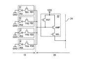
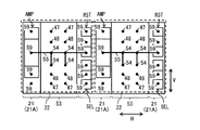
- 2 to 5 are diagrams showing an example of the sensor pixel 12 and the readout circuit 22.
- shared means that the outputs of the four sensor pixels 12 are input to the common readout circuit 22.
- the sharing unit does not matter the number of pixels.
- the output of one sensor pixel 12 may be input to one readout circuit 22.
- the outputs of the four sensor pixels 12 may be input to one readout circuit 22 as in the present example.
- each sensor pixel 12 has components common to each other.
- identification numbers 1, 2, 3, and 4 are added to the end of the reference numerals of the constituent elements of each sensor pixel 12.
- an identification number is given to the end of the reference numeral of the constituent element of each sensor pixel 12.
- the identification number at the end of the reference numeral of the constituent element of each sensor pixel 12 is omitted.
- Each sensor pixel 12 has, for example, a photodiode PD, a transfer transistor TR electrically connected to the photodiode PD, and a floating diffusion that temporarily holds the charge output from the photodiode PD via the transfer transistor TR. FD and.
- the photodiode PD corresponds to a specific but not limitative example of “photoelectric conversion element” of the present disclosure.
- the photodiode PD performs photoelectric conversion to generate electric charges according to the amount of received light.
- the cathode of the photodiode PD is electrically connected to the source of the transfer transistor TR, and the anode of the photodiode PD is electrically connected to a reference potential line such as a ground line (GND).
- the drain of the transfer transistor TR is electrically connected to the floating diffusion FD, and the gate of the transfer transistor TR is electrically connected to the pixel drive line 23 (see FIG. 1).
- the transfer transistor TR is, for example, a CMOS transistor.
- the floating diffusions FD of the sensor pixels 12 that share one readout circuit 22 are electrically connected to each other and also to the input end of the common readout circuit 22.
- the read circuit 22 has, for example, a reset transistor RST, a selection transistor SEL, and an amplification transistor AMP.
- the selection transistor SEL may be omitted if necessary.
- the source of the reset transistor RST, which is the input terminal of the read circuit 22, is electrically connected to the floating diffusion FD, and the drain of the reset transistor RST is electrically connected to the power supply line VDD and the drain of the amplification transistor AMP.
- the gate of the reset transistor RST is electrically connected to the pixel drive line 23 (see FIG. 1).
- the source of the amplification transistor AMP is electrically connected to the drain of the selection transistor SEL, and the gate of the amplification transistor AMP is electrically connected to the source of the reset transistor RST.
- the source of the selection transistor SEL which is the output terminal of the readout circuit 22, is electrically connected to the vertical signal line 24, and the gate of the selection transistor SEL is electrically connected to the pixel drive line 23 (see FIG. 1). ..
- the transfer transistor TR When the transfer transistor TR is turned on, the charge of the photodiode PD is transferred to the floating diffusion FD.
- the reset transistor RST resets the potential of the floating diffusion FD to a predetermined potential.
- the potential of the floating diffusion FD is reset to the potential of the power supply line VDD.
- the selection transistor SEL controls the output timing of the pixel signal from the readout circuit 22.
- the amplification transistor AMP generates, as a pixel signal, a signal having a voltage corresponding to the level of electric charges held in the floating diffusion FD.
- the amplification transistor AMP constitutes a source follower type amplifier, and outputs a pixel signal having a voltage corresponding to the level of the charge generated in the photodiode PD.
- the amplification transistor AMP When the selection transistor SEL is turned on, the amplification transistor AMP amplifies the potential of the floating diffusion FD and outputs a voltage corresponding to the potential to the column signal processing circuit 34 via the vertical signal line 24.
- the reset transistor RST, the amplification transistor AMP, and the selection transistor SEL are CMOS transistors, for example.
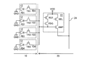
- the selection transistor SEL may be provided between the power supply line VDD and the amplification transistor AMP.
- the drain of the reset transistor RST is electrically connected to the power supply line VDD and the drain of the selection transistor SEL.
- the source of the selection transistor SEL is electrically connected to the drain of the amplification transistor AMP, and the gate of the selection transistor SEL is electrically connected to the pixel drive line 23 (see FIG. 1).
- the source of the amplification transistor AMP which is the output terminal of the read circuit 22, is electrically connected to the vertical signal line 24, and the gate of the amplification transistor AMP is electrically connected to the source of the reset transistor RST.
- the FD transfer transistor FDG may be provided between the source of the reset transistor RST and the gate of the amplification transistor AMP.
- the FD transfer transistor FDG is used when switching the conversion efficiency.
- the pixel signal is small when shooting in a dark place.
- the pixel signal becomes large. Therefore, if the FD capacitance C is not large, the floating diffusion FD cannot receive the charge of the photodiode PD.
- the FD capacitance C needs to be large so that the voltage V when converted by the amplification transistor AMP does not become too large. From these points of view, when the FD transfer transistor FDG is turned on, the gate capacitance for the FD transfer transistor FDG increases, so that the entire FD capacitance C increases. On the other hand, when the FD transfer transistor FDG is turned off, the entire FD capacitance C becomes small. In this way, by switching the FD transfer transistor FDG on/off, the FD capacitance C can be made variable and the conversion efficiency can be switched.
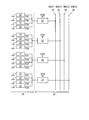
- FIG. 6 is a diagram showing an example of a connection mode of the plurality of read circuits 22 and the plurality of vertical signal lines 24.
- the plurality of vertical signal lines 24 may be assigned to each of the read circuits 22 one by one. ..
- the four vertical signal lines 24 are assigned to each read circuit 22 one by one. It may be.
- identification numbers 1, 2, 3, and 4 are given to the end of the reference numerals of each vertical signal line 24.
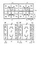
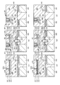
- FIGS. 7 and 8 are diagrams showing an example of a horizontal cross-sectional configuration of the solid-state imaging device 1.
- the upper diagrams of FIGS. 7 and 8 are diagrams showing an example of a cross-sectional configuration in the horizontal direction of the first substrate 10 of FIG. 1.
- the lower diagrams of FIGS. 7 and 8 are diagrams illustrating an example of a cross-sectional configuration in the horizontal direction of the second substrate 20 of FIG. 1.
- FIG. 7 illustrates a configuration in which two sets of four 2 ⁇ 2 sensor pixels 12 are arranged in the second direction H
- FIG. 8 illustrates four sets of four 2 ⁇ 2 sensor pixels 12, A configuration in which they are arranged in the first direction V and the second direction H is illustrated.
- FIGS. 7 and 8 a diagram showing an example of the surface configuration of the semiconductor substrate 11 is superimposed on a diagram showing an example of the cross-sectional configuration of the first substrate 10 in FIG. 1 in the horizontal direction. .. Further, in the lower sectional views of FIGS. 7 and 8, a diagram showing an example of the surface configuration of the semiconductor substrate 21 is superimposed on a diagram showing an example of the sectional configuration of the second substrate 20 in the horizontal direction of FIG. There is.
- the plurality of through-wirings 54, the plurality of through-wirings 48, and the plurality of through-wirings 47 are the first direction V which is the vertical direction in FIG. Alternatively, they are arranged side by side in a strip shape in the second direction H, which is the left-right direction in FIG. 7 and 8, a plurality of through wirings 54, a plurality of through wirings 48 and a plurality of through wirings 47 are arranged in two rows in the first direction V or the second direction H by way of example. Has been done.
- the first direction V or the second direction H is parallel to, for example, a column direction that is one of the two arrangement directions of the plurality of sensor pixels 12 arranged in a matrix, which are the row direction and the column direction. ing.
- the four floating diffusions FD are arranged close to each other, for example, via the pixel separation unit 43.
- the gate electrodes TG of the four transfer transistors TR are arranged so as to surround the four floating diffusions FD.
- the four gate electrodes TG form a ring shape. Is becoming
- the insulating layer 53 existing in the portion of the semiconductor substrate 21 through which the plurality of through wirings 54 penetrate is composed of a plurality of blocks extending in the first direction V or the second direction H.
- the semiconductor substrate 21 extends in the first direction V or the second direction H, and has a plurality of island shapes arranged side by side in the first direction V or the second direction H which are orthogonal to each other via the insulating layer 53. It is composed of a block 21A.
- Each block 21A is provided with, for example, a plurality of sets of reset transistors RST, amplification transistors AMP, and selection transistors SEL.
- the one readout circuit 22 shared by the four sensor pixels 12 is composed of, for example, a reset transistor RST, an amplification transistor AMP, and a selection transistor SEL in a region facing the four sensor pixels 12.
- One read circuit 22 shared by the four sensor pixels 12 includes, for example, an amplification transistor AMP in a block 21A on the left side of the insulating layer 53 and a reset transistor RST in a block 21A on the right side of the insulating layer 53. And a selection transistor SEL.
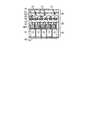
- 9 to 12 are diagrams showing an example of a wiring layout in the horizontal plane of the solid-state imaging device 1.
- 9 to 12 exemplify a case where one readout circuit 22 shared by the four sensor pixels 12 is provided in a region facing the four sensor pixels 12.
- the wirings shown in FIGS. 9 to 12 are provided, for example, in different wiring layers (not shown) provided on the pixel transistor described above.
- the wiring layer is, for example, a plurality of pixel drive lines 23 and a plurality of vertical signal lines 24, a pad electrode (not shown) exposed on the surface of the wiring layer and used for electrical connection between the second substrate 20 and the third substrate 30. have.
- the four penetrating wirings 54 adjacent to each other are electrically connected to the connecting wiring 55, for example, as shown in FIG.
- the four penetrating wirings 54 adjacent to each other are further connected to the gate of the amplification transistor AMP included in the left adjacent block 21A of the insulating layer 53 and the right adjacent block of the insulating layer 53, for example, via the connection wiring 55 and the connection portion 59. It is electrically connected to the gate of the reset transistor RST included in 21A.
- the power supply line VDD is arranged at a position facing each read circuit 22 arranged side by side in the second direction H, as shown in FIG. 10, for example.
- the power supply line VDD is electrically connected to the drain of the amplification transistor AMP and the drain of the reset transistor RST of the read circuits 22 arranged side by side in the second direction H, for example, via the connection portion 59.
- the two pixel drive lines 23 are arranged at positions facing the respective readout circuits 22 arranged side by side in the second direction H.
- One pixel drive line 23 is, for example, a wiring RSTG electrically connected to the gate of the reset transistor RST of each readout circuit 22 arranged side by side in the second direction H.
- the other pixel drive line 23 is, for example, a wiring SELG electrically connected to the gate of the selection transistor SEL of each readout circuit 22 arranged side by side in the second direction H.
- the source of the amplification transistor AMP and the drain of the selection transistor SEL are electrically connected to each other, for example, via the wiring 25.
- the two power supply lines VSS are arranged, for example, at positions facing the respective read circuits 22 arranged side by side in the second direction H.
- Each power supply line VSS is electrically connected to the plurality of through wirings 47, for example, at a position facing each sensor pixel 12 arranged side by side in the second direction H.
- the four pixel drive lines 23 are arranged at positions facing the respective readout circuits 22 arranged side by side in the second direction H.
- Each of the four pixel drive lines 23 is electrically connected to the through wiring 48 of one of the four sensor pixels 12 corresponding to the readout circuits 22 arranged in the second direction H, for example.
- the wiring TRG connected to.
- the four pixel drive lines 23 functioning as control lines are electrically connected to the gate electrodes TG of the transfer transistors TR of the sensor pixels 12 arranged in the second direction H.
- identifiers 1, 2, 3, 4 are added to the end of each wiring TRG.
- the vertical signal line 24 is arranged, for example, at a position facing the read circuits 22 arranged side by side in the first direction V.
- the vertical signal line 24 that functions as an output line is electrically connected to, for example, the source of the amplification transistor AMP, which is the output terminal of each read circuit 22 arranged side by side in the first direction V.
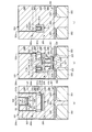
- FIGS. 13 and 14 are diagrams showing a modification of the horizontal sectional configuration of the solid-state imaging device 1.
- the upper drawings of FIGS. 13 and 14 are modifications of the horizontal cross-sectional configuration of the first substrate 10 of FIG. 1, and the lower drawings of FIG. 13 are the horizontal direction of the second substrate 20 of FIG. 5 is a modification of the cross-sectional configuration in FIG.
- a modified example of the surface configuration of the semiconductor substrate 11 of FIG. 1 is shown in a diagram showing a modified example of the sectional configuration of the first substrate 10 in the horizontal direction of FIG.
- the representations are overlaid.
- a diagram showing a modified example of the sectional configuration of the second substrate 20 in the horizontal direction of FIG. 1 and a diagram showing a modified example of the surface configuration of the semiconductor substrate 21. Are overlaid.
- the plurality of through wirings 54, the plurality of through wirings 48, and the plurality of through wirings 47 which are shown as a plurality of dots arranged in a matrix in the drawings, are formed on the first substrate 10. 13A and 13B, the strips are arranged side by side in the first direction H, which is the left-right direction in FIGS. 13 and 14 exemplify a case where the plurality of through wirings 54, the plurality of through wirings 48, and the plurality of through wirings 47 are arranged side by side in two rows in the second direction H.
- the four floating diffusions FD are arranged close to each other, for example, via the pixel separation unit 43.
- the four transfer gates TG1, TG2, TG3, and TG4 are arranged so as to surround the four floating diffusions FD.
- the four transfer gates TG form a ring. It has a shape.
- the insulating layer 53 is composed of a plurality of blocks extending in the second direction H.
- the semiconductor substrate 21 includes a plurality of island-shaped blocks 21A extending in the second direction H and arranged side by side in the first direction V orthogonal to the second direction H with the insulating layer 53 interposed therebetween. ..
- Each block 21A is provided with, for example, a reset transistor RST, an amplification transistor AMP, and a selection transistor SEL.
- the one readout circuit 22 shared by the four sensor pixels 12 is, for example, not arranged so as to face the four sensor pixels 12 but is displaced in the first direction V.
- one read circuit 22 shared by four sensor pixels 12 is a reset transistor in a region of the second substrate 20 facing the four sensor pixels 12 in the first direction V. It is composed of an RST, an amplification transistor AMP, and a selection transistor SEL.
- One readout circuit 22 shared by the four sensor pixels 12 is configured by, for example, the amplification transistor AMP, the reset transistor RST, and the selection transistor SEL in one block 21A.
- one read circuit 22 shared by four sensor pixels 12 is a reset transistor in a region of the second substrate 20 which is opposed to the four sensor pixels 12 in the first direction V.
- One readout circuit 22 shared by the four sensor pixels 12 is configured by, for example, the amplification transistor AMP, the reset transistor RST, the selection transistor SEL, and the FD transfer transistor FDG in one block 21A.
- the one readout circuit 22 shared by the four sensor pixels 12 is not arranged, for example, so as to face the four sensor pixels 12 first, but from the position directly facing the four sensor pixels 12. They are arranged so as to be displaced in the direction V.
- the wiring 25 (see FIG. 10) can be shortened, or the wiring 25 can be omitted and the source of the amplification transistor AMP and the drain of the selection transistor SEL can be formed in a common impurity region. It can also be configured. As a result, it is possible to reduce the size of the read circuit 22 and increase the size of other parts in the read circuit 22.
- FIG. 15 is a diagram showing a modification of the horizontal sectional configuration of the solid-state imaging device 1.
- FIG. 15 shows a modification of the sectional configuration of FIG. 7.
- the semiconductor substrate 21 is composed of a plurality of island-shaped blocks 21A arranged side by side in the first direction V and the second direction H with the insulating layer 53 interposed therebetween.
- Each block 21A is provided with, for example, a set of a reset transistor RST, an amplification transistor AMP, and a selection transistor SEL.
- RST reset transistor
- AMP amplification transistor
- SEL selection transistor
- FIG. 16 is a diagram showing a modification of the horizontal sectional configuration of the solid-state imaging device 1.
- FIG. 16 shows a modification of the sectional configuration of FIG.
- one read circuit 22 shared by the four sensor pixels 12 is not arranged, for example, directly facing the four sensor pixels 12, but is arranged in the first direction V with a shift.
- the semiconductor substrate 21 is composed of a plurality of island-shaped blocks 21A arranged side by side in the first direction V and the second direction H with the insulating layer 53 interposed therebetween. There is.
- Each block 21A is provided with, for example, a set of a reset transistor RST, an amplification transistor AMP, and a selection transistor SEL.
- the plurality of through wirings 47 and the plurality of through wirings 54 are also arranged in the second direction H.
- the plurality of through wirings 47 share four through wirings 54 that share a certain read circuit 22 and four through wirings that share another read circuit 22 adjacent to the read circuit 22 in the second direction H. 54 and 54.
- the crosstalk between the read circuits 22 adjacent to each other can be suppressed by the insulating layer 53 and the through wiring 47, and the deterioration of the resolution on the reproduced image and the deterioration of the image quality due to color mixture can be suppressed.
- FIG. 17 is a diagram showing an example of a horizontal cross-sectional configuration of the solid-state imaging device 1 described above.
- FIG. 17 shows a modification of the sectional configuration of FIG.
- the first substrate 10 has the photodiode PD and the transfer transistor TR for each sensor pixel 12, and the floating diffusion FD is shared by each of the four sensor pixels 12. Therefore, in this modification, one through wiring 54 is provided for each of the four sensor pixels 12.
- the unit area corresponding to four sensor pixels 12 sharing one floating diffusion FD can be obtained by shifting one sensor pixel 12 in the first direction V.
- the four sensor pixels 12 corresponding to the area will be referred to as four sensor pixels 12A.
- the first substrate 10 shares the through wiring 47 for each of the four sensor pixels 12A. Therefore, in this modification, one through wiring 47 is provided for each of the four sensor pixels 12A.
- the first substrate 10 has a pixel separation unit 43 that separates the photodiode PD and the transfer transistor TR for each sensor pixel 12.
- the pixel separating unit 43 does not completely surround the sensor pixel 12 when viewed from the normal line direction of the semiconductor substrate 11, and is provided near the through wiring 54 connected to the floating diffusion FD and near the through wiring 47. It has a gap that is an unformed region. The gap allows the four sensor pixels 12 to share one through wiring 54 and the four sensor pixels 12A to share one through wiring 47.
- the second substrate 20 has the readout circuit 22 for each of the four sensor pixels 12 that share the floating diffusion FD.
- FIG. 18 is a diagram showing an example of a horizontal sectional configuration of the solid-state imaging device 1 according to the present modification.
- FIG. 18 shows a modification of the sectional configuration of FIG.
- the first substrate 10 has the photodiode PD and the transfer transistor TR for each sensor pixel 12, and the floating diffusion FD is shared by each of the four sensor pixels 12. Further, the first substrate 10 has a pixel separation section 43 that separates the photodiode PD and the transfer transistor TR for each sensor pixel 12.
- FIG. 19 is a diagram showing an example of a horizontal sectional configuration of the solid-state imaging device 1 according to the present modification.
- FIG. 19 shows a modification of the sectional configuration of FIG.
- the first substrate 10 has the photodiode PD and the transfer transistor TR for each sensor pixel 12, and the floating diffusion FD is shared by each of the four sensor pixels 12. Further, the first substrate 10 has a pixel separation section 43 that separates the photodiode PD and the transfer transistor TR for each sensor pixel 12.
- FIG. 20 is a diagram showing an example of a circuit configuration of the solid-state image sensor 1 according to the modification.
- the solid-state image sensor 1 according to the present modification is a CMOS image sensor equipped with a column parallel ADC.
- a vertical drive circuit 33 in addition to the pixel region 13 in which a plurality of sensor pixels 12 including photoelectric conversion elements are two-dimensionally arranged in a matrix, a vertical drive circuit 33, It has a configuration including a column signal processing circuit 34, a reference voltage supply unit 38, a horizontal drive circuit 35, a horizontal output line 37, and a system control circuit 36.
- the system control circuit 36 uses the master clock MCK as a reference clock signal for operations of the vertical drive circuit 33, the column signal processing circuit 34, the reference voltage supply section 38, the horizontal drive circuit 35, and the like.
- a control signal or the like is generated and given to the vertical drive circuit 33, the column signal processing circuit 34, the reference voltage supply unit 38, the horizontal drive circuit 35, and the like.
- the vertical drive circuit 33 is also formed on the first substrate 10 together with each sensor pixel 12 in the pixel region 13, and is also formed on the second substrate 20 on which the readout circuit 22 is formed.
- the column signal processing circuit 34, the reference voltage supply unit 38, the horizontal drive circuit 35, the horizontal output line 37, and the system control circuit 36 are formed on the third substrate 30.
- the read circuit 22 includes, for example, a reset transistor RST that controls the potential of the floating diffusion FD, an amplification transistor AMP that outputs a signal corresponding to the potential of the floating diffusion FD, and a pixel selection.
- a three-transistor configuration having a selection transistor SEL for performing the above can be used.
- the sensor pixels 12 are two-dimensionally arranged, and the pixel drive lines 23 are arranged in each row and the vertical signal lines 24 are arranged in each column with respect to the pixel arrangement of m rows and n columns. There is.
- One end of each of the plurality of pixel drive lines 23 is connected to each output end corresponding to each row of the vertical drive circuit 33.
- the vertical drive circuit 33 is configured by a shift register or the like, and controls the row address and the row scan of the pixel region 13 via the plurality of pixel drive lines 23.
- the column signal processing circuit 34 has, for example, ADCs (analog-digital conversion circuits) 34-1 to 34-m provided for each pixel column of the pixel region 13, that is, for each vertical signal line 24, and the pixel region 13 is provided.
- ADCs analog-digital conversion circuits
- the reference voltage supply unit 38 has, for example, a DAC (digital-analog conversion circuit) 38A as a method of generating a reference voltage Vref having a so-called ramp (RAMP) waveform, the level of which changes in an inclined manner as time passes. There is.
- the method of generating the reference voltage Vref having the ramp waveform is not limited to the DAC 38A.
- the DAC 38A under the control of the control signal CS1 given from the system control circuit 36, generates the ramp waveform reference voltage Vref based on the clock CK given from the system control circuit 36 to generate the ADC 34-1 of the column processing unit 15. Supply to ⁇ 34-m.
- each of the ADCs 34-1 to 34-m has an exposure time of 1/N of the sensor pixel 12 as compared with the normal frame rate mode in the progressive scanning method for reading out all the information of the sensor pixel 12 and the normal frame rate mode. Is set so that the AD conversion operation corresponding to each operation mode such as the high-speed frame rate mode for increasing the frame rate N times, for example, twice, can be selectively performed.
- the switching of the operation mode is executed by the control by the control signals CS2 and CS3 provided from the system control circuit 36. Further, the system control circuit 36 is provided with instruction information for switching between the normal frame rate mode and each operation mode of the high speed frame rate mode from an external system controller (not shown).
- the ADCs 34-1 to 34-m have the same configuration, and the ADC 34-m will be described as an example here.
- the ADC 34-m is configured to include a comparator 34A, a counting unit such as an up/down counter (U/DCNT) 34B, a transfer switch 34C, and a memory device 34D.
- the comparator 34A includes a signal voltage Vx of the vertical signal line 24 corresponding to a signal output from each sensor pixel 12 in the nth column of the pixel region 13 and a reference voltage Vref of a ramp waveform supplied from the reference voltage supply unit 38. And the output voltage Vco becomes “H” level when the reference voltage Vref becomes higher than the signal voltage Vx, and the output voltage Vco becomes “L” level when the reference voltage Vref is equal to or lower than the signal voltage Vx. ..
- the up/down counter 34B is an asynchronous counter, and under the control of the control signal CS2 given from the system control circuit 36, the clock CK is given from the system control circuit 36 at the same time as the DAC 18A, and is down in synchronization with the clock CK ( By performing the DOWN) count or the UP (UP) count, the comparison period from the start of the comparison operation in the comparator 34A to the end of the comparison operation is measured.
- the comparison time at the first read time is measured by counting down during the first read operation, and the second read operation is performed.
- the comparison time at the second read is measured by counting up during the read operation.
- the count result for the sensor pixel 12 in a certain row is held as it is, and then the sensor pixel 12 in the next row is down-counted at the first read operation from the previous count result.
- the comparison time at the time of the first read is measured, and by counting up at the time of the second read operation, the comparison time at the time of the second read is measured.
- the transfer switch 34C is turned on when the count operation of the up/down counter 34B for the sensor pixel 12 in a certain row is completed in the normal frame rate mode ( In the closed state, the count result of the up/down counter 34B is transferred to the memory device 34D.
- the analog signal supplied from each sensor pixel 12 in the pixel region 13 via the vertical signal line 24 for each column is supplied to the comparator 34A and the up/down counter 34B in the ADCs 34-1 to 34-m. By each operation, it is converted into an N-bit digital signal and stored in the memory device 34D.
- the horizontal drive circuit 35 is composed of a shift register or the like, and controls the column address and column scan of the ADCs 34-1 to 34-m in the column signal processing circuit 34. Under the control of the horizontal drive circuit 35, the N-bit digital signal AD-converted by each of the ADCs 34-1 to 34-m is sequentially read out to the horizontal output line 37, and passes through the horizontal output line 37. It is output as imaging data.
- a circuit or the like for performing various kinds of signal processing on the imaging data output via the horizontal output line 37 may be provided in addition to the above-described constituent elements. Is.
- the count result of the up/down counter 34B can be selectively transferred to the memory device 34D via the transfer switch 34C. It is possible to independently control the count operation of the /down counter 34B and the read operation of the count result of the up/down counter 34B to the horizontal output line 37.
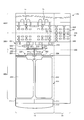
- FIG. 21 shows an example in which the solid-state imaging device 1 of FIG. 20 is configured by laminating three substrates of a first substrate 10, a second substrate 20, and a third substrate 30.
- a pixel region 13 including a plurality of sensor pixels 12 is formed in the central portion of the first substrate 10, and a vertical drive circuit 33 is formed around the pixel region 13.
- a read circuit area 15 including a plurality of read circuits 22 is formed in the central portion, and a vertical drive circuit 33 is formed around the read circuit area 15.
- the column signal processing circuit 34, the horizontal drive circuit 35, the system control circuit 36, the horizontal output line 37, and the reference voltage supply unit 38 are formed on the third substrate 30.
- the vertical drive circuit 33 may be formed only on the first substrate 10 or only on the second substrate 20.
- FIG. 22 shows a modification of the cross-sectional configuration of the solid-state imaging device 1 according to this modification.
- the solid-state imaging device 1 is configured by stacking three substrates of the first substrate 10, the second substrate 20, and the third substrate 30.
- the solid-state imaging device 1 may be configured by stacking two substrates, the first substrate 10 and the second substrate 20.
- the logic circuit 32 is formed separately on the first substrate 10 and the second substrate 20, as shown in FIG. 22, for example.
- a high dielectric constant film made of a material (for example, high-k) that can withstand a high temperature process and a metal gate electrode are laminated.
- a transistor having a gate structure is provided.
- CoSi 2 or NiSi formed using a self-aligned silicide (SALICIDE) process on the surface of the impurity diffusion region in contact with the source electrode and the drain electrode.
- SALICIDE self-aligned silicide
- a low resistance region made of silicide or the like is formed. The low resistance region made of silicide is thus formed of the compound of the material of the semiconductor substrate and the metal.
- FIG. 23 shows a modification of the cross-sectional structure of the solid-state imaging device 1 according to the structure of FIG. 1 and its modification.
- a self-aligned silicide (SALICIDE) process is formed on the surface of the impurity diffusion region in contact with the source electrode and the drain electrode.
- the low resistance region 37 made of silicide such as CoSi 2 or NiSi may be formed. This allows a high temperature process such as thermal oxidation to be used when forming the sensor pixel 12.
- the contact resistance can be reduced. As a result, the calculation speed in the logic circuit 32 can be increased.
- FIG. 24 is a diagram showing a part of the cross section of the solid-state imaging device 100 according to the first embodiment of the present disclosure.
- the solid-state imaging device 100 has a structure in which a laminated body 200, a laminated body 300, and a laminated body 400 are bonded together.
- a surface 230 shown in FIG. 24 is a surface on which the laminated body 200 and the laminated body 300 are bonded together.
- a surface 340 shown in FIG. 24 is a surface on which the laminated body 300 and the laminated body 400 are attached.
- a color filter 211 is arranged below the stacked bodies 200 to 400, that is, at the lower end of the stacked body 200.
- An on-chip lens 212 is arranged below the color filter 211.
- the on-chip lens 212 collects the emitted light.
- the condensed light is guided to the photoelectric conversion element 203 included in the stacked body 200 via the color filter 211.
- the stacked body 200 has a structure in which a plurality of films that form transistors and the like are stacked on a substrate 201.
- the substrate 201 is a semiconductor substrate such as an N-type silicon substrate.
- a P-type semiconductor region 202 (P well) is formed on the substrate 200.
- An N-type semiconductor region is formed in the semiconductor region 202, whereby a photoelectric conversion element 203 such as a photodiode having a PN junction is formed.
- the photoelectric conversion element 203 converts the received light into an electric signal according to the received light amount by photoelectric conversion.
- a HAD (Hole Accumulation Diode) 204 which is a P + type semiconductor region, is formed above the photoelectric conversion element 203.
- the HAD 204 functions as a hole storage layer and suppresses dark current generated from the surface of the photoelectric conversion element 203, which is an N-type photodiode.
- the N-type transfer transistor 220 is arranged on the substrate 201.
- the transfer transistor 220 includes a floating diffusion (FD) 221 which is an N type source region.
- the transfer transistor 220 transfers the electric signal output from the photoelectric conversion element 203 to the pixel transistor.
- the FD 221 temporarily holds the electric signal output from the photoelectric conversion element 203.
- the transfer transistor 220 including the FD 221 and the HAD 204 are covered with an insulating film 250.
- the laminated body 300 has a structure in which a plurality of films forming transistors and the like are laminated on a substrate 301.
- the substrate 301 is a semiconductor substrate such as a P-type silicon substrate.
- the stacked body 300 is turned upside down and is laminated on the insulating film 250 of the stacked body 200.
- pixel transistors such as an N-type amplification transistor 310, an N-type reset transistor 320, and an N-type selection transistor (not shown) are arranged. ..
- the pixel transistor performs a process of reading an electric signal according to the amount of light received by the photoelectric conversion element 203.
- a wiring 313d is connected to the gate electrode 313 of the amplification transistor 310.
- the wiring 313d is connected to the source region 321 of the reset transistor 320.
- the wiring 313d is connected to the FD 221 of the transfer transistor 320 via the contact 221c.
- the pixel transistors such as the amplification transistor 310 and the reset transistor 320 are covered with the insulating film 350. That is, the insulating film 250 and the insulating film 350 are bonded to each other on the surface 230 where the stacked body 200 and the stacked body 300 are attached to each other.
- Wirings D1 to D4 are formed in four layers on the lower surface of the substrate 301, that is, on the side opposite to the side on which the pixel transistors are arranged.
- the wiring D1 is a wiring formed in the lowermost layer of the first layer.
- the wiring D4 is a wiring formed in the uppermost layer of the fourth layer. Note that the number of wiring layers is not limited to four, and can be arbitrarily changed according to design conditions and the like.
- the wirings D1 to D4 are covered with the insulating film 360.
- the laminated body 400 has a structure in which a plurality of films forming transistors and the like are laminated on a substrate 401.
- the substrate 401 is a semiconductor substrate such as a silicon substrate.
- the stacked body 400 is turned upside down and bonded onto the wiring D4 of the stacked body 300. In the example of FIG. 24, the junction point 402 between the wiring D4 and the wiring of the stacked body 400 overlaps the pixel area in which the pixel is arranged.
- a plurality of logic transistors Tr arranged on the substrate 401, that is, on the side of the substrate 401 facing the substrate 301 is connected to the wiring of the stacked body 400.
- the wiring of the stacked body 400 and the logic transistor Tr are covered with the insulating film 450.
- a logic circuit is configured by the wiring of the stacked body 400 and the logic transistor Tr.
- the logic circuit corresponds to a peripheral circuit of the solid-state image sensor 100 that processes an electric signal or the like generated by the photoelectric conversion element 203.
- FIG. 25 is a schematic diagram illustrating the vicinity of the bonding position of the stacked bodies 200 and 300 of the solid-state imaging device 100 according to the first embodiment of the present disclosure.
- 25A is a top view of the laminated body 300 on the side where the pixel transistors are formed
- FIGS. 25B to 25D are cross-sectional views showing the vicinity of the bonding positions of the laminated bodies 200 and 300
- FIG. 25A is a top view of the laminated body 300 on the side where the pixel transistors are formed
- FIGS. 25B to 25D are cross-sectional views showing the vicinity of the bonding positions of the laminated bodies 200 and 300
- the solid-state imaging device 100 includes a substrate 201 as a first semiconductor substrate having an FD 221 that temporarily holds an electric signal output from the photoelectric conversion element 203.
- the HAD 204 is arranged on the photoelectric conversion element 203.
- a contact 204c connected to the upper layer wiring is connected to the HAD 204.
- the contact 204c is grounded through the upper wiring to fix the substrate potential of the substrate 201 to 0V.
- the FD 221 is a source region of the transfer transistor 220.
- the transfer transistor 220 includes a gate insulating film 224 arranged on the substrate 201 and a gate electrode 223 arranged on the gate insulating film 224.
- a contact 223c connected to the upper wiring is connected to the gate electrode 223.
- the contact 223c is connected to the peripheral circuit including the logic transistor Tr via the upper layer wiring and the wiring of the stacked body 400.
- the transfer transistor 220 transfers the electric signal output from the photoelectric conversion element 203 to the amplification transistor 310.
- the solid-state imaging device 100 includes a substrate 301 as a second semiconductor substrate facing the substrate 201.
- the substrate 301 includes the amplification transistor 310 as the first transistor on the side facing the substrate 201.
- the amplification transistor 310 includes a channel 315 extending in the thickness direction of the substrate 301 and a gate electrode 313 as a multi-gate extending in the thickness direction of the substrate 301 and sandwiching the channel 315.
- the channel 315 is composed of a part of the substrate 301, and becomes a current path between a source region 311 and a drain region 312, which will be described later, when a voltage is applied to the gate electrode 313.
- a gate insulating film 314 is interposed between the channel 315 and the gate electrode 313.
- the amplification transistor 310 is configured as, for example, a tri-gate transistor in which the gate electrode 313 is connected to the channel 315 via the gate insulating film 314 on three surfaces.
- the amplification transistor 310 amplifies and outputs the electric signal transferred from the photoelectric conversion element 203 by the transfer transistor 220.
- the substrate 301 includes a reset transistor 320 as a second transistor including a source region 322 on the side facing the substrate 201.
- the reset transistor 320 includes a channel 325 extending in the thickness direction of the substrate 301 and a gate electrode 323 as a multi-gate extending in the thickness direction of the substrate 301 and sandwiching the channel 325.
- the channel 325 is composed of a part of the substrate 301, and when a voltage is applied to the gate electrode 313, it becomes a current path between a source region 321 and a drain region 322, which will be described later.
- a gate insulating film 324 is interposed between the channel 325 and the gate electrode 323.
- the reset transistor 320 is configured as, for example, a tri-gate transistor in which the gate electrode 323 is connected to the channel 325 via the gate insulating film 324 on three surfaces.
- the reset transistor 320 resets (initializes) the potential of the gate electrode 313 of the amplification transistor 310 to the power source potential.
- the reset transistor 320 is also a transistor that resets the potential of the FD 221.
- the gate electrode 323 of the reset transistor 320 is connected to the wirings D1 to D4 as signal lines for transmitting electric signals from the surface side of the substrate 301 opposite to the surface facing the substrate 201. Specifically, the gate electrode 323 is connected to the wirings D1 to D4 via the contact 323c. The wirings D1 to D4 are connected to a peripheral circuit including the logic transistor Tr via the wiring of the stacked body 400 and exchange electric signals.
- the substrate 301 includes a selection transistor 330 on the side facing the substrate 201.
- the selection transistor 330 includes a channel 335 extending in the thickness direction of the substrate 301 and a gate electrode 333 as a multi-gate extending in the thickness direction of the substrate 301 and sandwiching the channel 335.
- the channel 335 is composed of a part of the substrate 301, and when a voltage is applied to the gate electrode 313, it becomes a current path between a source region 331 and a drain region 332.
- a gate insulating film 334 is interposed between the channel 335 and the gate electrode 333.
- the selection transistor 330 is configured as, for example, a tri-gate transistor in which the gate electrode 333 is connected to the channel 335 via the gate insulating film 334 on three surfaces. Since the selection transistor 330 processes the electric signal amplified by the amplification transistor 310, it selects whether or not to transmit the electric signal to the wirings D1 to D4 in the upper layer.
- the gate electrode 313 of the amplification transistor 310 and the gate electrode 333 of the selection transistor 330 are arranged in parallel.
- the gate electrode 333 of the selection transistor 330 and the gate electrode 323 of the reset transistor 320 are arranged so as to be orthogonal to each other.
- the gate electrode 313 of the amplification transistor 310 is connected to the FD 221.
- the solid-state imaging device 100 includes a contact 221c that connects the facing surfaces of the gate electrode 313 and the FD 221. That is, in the example of FIG. 25, of the gate electrodes 313 extending toward the substrate 201 in the thickness direction of the substrate 301, the surface closest to the substrate 201 and the substrate 201 of the FD 221 arranged on the surface layer of the substrate 201. Is connected to the outermost surface by a contact 221c such as polysilicon. In other words, the contact 221c connects the gate electrode 313 and the FD 221 with the shortest distance.
- the gate electrode 313 of the amplification transistor 310 is connected to the source region 321 of the reset transistor 320. Specifically, the gate electrode 313 of the amplification transistor 310 extends in the direction of the reset transistor 320 to form the wiring 313d. The gate electrode 313 of the amplification transistor 310 and the source region 321 of the reset transistor 320 are connected by a wiring 313d.
- the substrate 301 includes source regions 311 and 331 that reach from one surface side of the substrate 301 to the other surface side, and from one surface side of the substrate 301 to the other surface side. Drain regions 312, 322, 333 reaching The source region 311 and the drain region 312 have an N-type conductivity type with an impurity concentration of, for example, 1 ⁇ 10 18 cm ⁇ 3 or more, and are included in the amplification transistor 310.
- the source region 331 and the drain region 332 have an N-type conductivity type with an impurity concentration of, for example, 1 ⁇ 10 18 cm ⁇ 3 or more, and are included in the selection transistor 330.
- the drain region 332 of the selection transistor 330 is connected to the source region 311 of the amplification transistor 310.
- the drain region 322 has an N type conductivity type with an impurity concentration of, for example, 1 ⁇ 10 18 cm ⁇ 3 or more, and is included in the reset transistor 320.
- the source region 321 of the reset transistor 320 also has an N-type conductivity.
- the source region 321 of the reset transistor 320 is formed only on the surface layer portion of the substrate 301 on the side facing the substrate 201, and does not reach the surface on the opposite side of the substrate 301.
- a region from the FD 221 to the source region 321 of the reset transistor 320 via the contact 221c, the gate electrode 313 of the amplification transistor 310, and the wiring 313d is an FD region functioning as a floating diffusion.
- the source region 321 is formed smaller than the others so as to prevent the FD capacitance from increasing.
- the source regions 311 and 331 are connected to wirings D1 to D4 as signal lines for transmitting electric signals from the surface side of the substrate 301 opposite to the surface facing the substrate 201. Specifically, the source region 311 is connected to the wirings D1 to D4 via the contact 311c. The source region 331 is connected to the wirings D1 to D4 via the contact 331c. The wirings D1 to D4 are connected to a peripheral circuit including the logic transistor Tr via the wiring of the stacked body 400 and exchange electric signals.
- the drain regions 312, 322, 333 are connected to the power supply potential from the surface side of the substrate 301 opposite to the surface facing the substrate 201.
- the drain region 312 is connected to the wirings D1 to D4 via the contact 312c.
- the drain region 322 is connected to the wirings D1 to D4 via the contact 322c.
- the drain region 332 is connected to the wirings D1 to D4 via the contact 332c.
- the wirings D1 to D4 are connected to the power supply potential.
- the pixel transistor arranged on the substrate 301 is configured as a tri-gate transistor, for example.
- the configuration of the tri-gate transistor will be described in more detail with reference to FIG. 26 by taking the amplification transistor 310 as an example.
- the reset transistor 320 and the selection transistor 330 are also configured similarly to the amplification transistor 310 described below.
- FIG. 26 is a schematic diagram showing a configuration of the amplification transistor 310 according to the first embodiment of the present disclosure.
- 26A is an exploded perspective view of the amplification transistor 310
- FIG. 26B is a perspective view of the amplification transistor 310.
- the source region 311, the drain region 312, and the channel 314 sandwiched between them are formed in an upright plate shape along the stacking direction SD of the stacked body 300.
- the gate insulating film 314 is, for example, a High-k material such as Al 2 O 3 , TiO 2 , Ta 2 O 5 , HfO 2 , HfSiON, HfSiO 4 , ZrO 2 , ZrSiO 4 , La 2 O 3 , Y 2 O 3 or the like. Composed of.
- the gate insulating film 314 is covered with the gate electrode 313.
- the gate electrode 313 is made of, for example, polysilicon.
- the amplification transistor 313 may be a metal gate transistor whose gate electrode 313 is made of a metal-based material such as TaCx, W, WNx, or TiN.
- the gate width is the sum of the width of the plate-shaped channel (plate thickness) and the height ⁇ 2.
- the amplification transistor 310 has the N-type source region 311, the N-type drain region 312, and the P-type channel 315 sandwiched between these regions. Then, the insulating film 360 is arranged immediately below the body of the NPN structure of the amplification transistor 310. That is, the amplification transistor 310 has a fully depleted silicon-on-insulator (FD-SOI) structure.
- FD-SOI fully depleted silicon-on-insulator
- FIGS. 27 to 31 are flowcharts showing an example of the procedure of the manufacturing process of the solid-state imaging device 100 according to the first embodiment of the present disclosure.
- 27 to 31 are sectional views taken along the line AA′ of FIG. 25A in the manufacturing process of the solid-state imaging device 100.
- 27 to 31 are sectional views taken along the line BB′ of FIG. 25A in the manufacturing process of the solid-state imaging device 100.
- the right views of FIGS. 27 to 31 are sectional views taken along the line CC′ of FIG. 25A in the manufacturing process of the solid-state imaging device 100.
- a substrate 301 such as a P-type silicon substrate is subjected to element isolation, and then trenches TR are formed to form channels 315 and 325. Although not shown, the channel 335 is also formed at this time.
- gate insulating films 314, 324, 334 are formed so as to cover the channels 315, 325, 335. Further, gate electrodes 313, 323, 333 are formed so as to cover the gate insulating films 314, 324, 334.
- the N-type source regions 311, 321, 331 and the N-type drain regions 312, 322 are formed on the substrate 301 on both sides of the gate electrodes 313, 323, 333 so that the impurity concentration is 1 ⁇ 10 18 cm ⁇ 3 or more. , 332 are formed.
- the source regions 311, 331 and the drain regions 312, 322, 332 are formed to the depth of the trench TR.
- the source region 321 is formed shallower than the other source regions 311 and 331.
- the wiring 313d connecting the gate electrode 313 and the source region 321 is formed while the insulating film 350 covering each component is laminated on the substrate 301. ..
- the insulating film 350 is stacked until the entire structure including the wiring 313d is filled.
- a P-type semiconductor region 202 is formed on a substrate 201 such as an N-type silicon substrate, and a photoelectric conversion element 203 such as an N-type photodiode is formed. And a HAD 204, which is a P + type semiconductor region, is formed.
- the gate insulating film 224 is formed over the substrate 201, and the gate electrode 223 is formed over the gate insulating film 224. Then, the FD 221 as an N-type source region is formed on the substrate 201 near the gate electrode 223.
- the insulating film 250 is formed on the substrate 201 so as to cover each component.
- the substrate 301 described above is inverted on the substrate 201 on which each structure is formed, and the surface on which the pixel transistors are formed is arranged to face the substrate 201.
- the substrate 201 and the substrate 301 are attached to each other. At this time, the insulating film 250 formed on the substrate 201 and the insulating film 350 formed on the substrate 301 are bonded.
- the transfer transistor 220 on the substrate 201 and the pixel transistor on the substrate 301 face each other. Further, the wiring 313d extended from the gate electrode 313 is arranged immediately above the FD 221 on the substrate 201.
- the surface of the substrate 301 opposite to the side on which the pixel transistors are formed is ground to thin the substrate 301.
- the bulk substrate 301 disappears and the ends of the channels 315, 325, 335 opposite to the sides covered with the gate electrodes 313, 323, 333, the gate insulating films 314, 324, 334.
- the U-shaped both ends and the U-shaped both ends of the gate electrodes 313, 323, 333 are thinned until exposed.
- the bulk substrate 301 may be left.
- FIGS. 29(a1)(b1)(c1) when the bulk substrate 301 is eliminated, each pixel transistor has an FD-SOI structure.
- ground substrate 301 A part of the ground substrate 301 remains in a divided state around each pixel transistor, but these substrates 301 are not shown in the following figures.
- FIGS. 29(a2)(b2)(c2) the positions corresponding to the source regions 311,331 and the drain regions 312,322,332 from the surface of the substrate 301 opposite to the side where the pixel transistors are formed. Then, ion implantation or the like is performed so that the impurity concentration becomes 1 ⁇ 10 18 cm ⁇ 3 or more. Thereby, the source regions 311 and 331 and the drain regions 312, 322, and 332 that reach from the one surface side of the substrate 301 to the other surface side are obtained.
- an insulating film 360 covering each component is formed on the substrate 301. Then, a through hole TH penetrating the insulating films 360, 350, 250 and the wiring 313d and reaching the FD 221 of the substrate 201 is formed.
- the through hole TH is filled with a conductive material such as polysilicon up to the height of the wiring 313d to form a contact 221c connecting the wiring 313d and the FD 221.
- the insulating films 350 and 360 above the wiring 313d are backfilled with an insulating material such as SiO 2 .
- a contact 223c is formed on the gate electrode 223 and connected to the upper layer wiring.
- a contact 204c is formed on the HAD 204 and connected to the upper wiring.
- a contact 323c is formed on the gate electrode 323 and connected to the wirings D1 to D4.
- a contact 333c is also formed on the gate electrode 333 and connected to the wirings D1 to D4.
- contacts 311c and 331c are formed on the source regions 311 and 331 and connected to the wirings D1 to D4.
- Contacts 312c, 322c, 332c are formed on the drain regions 312, 322, 332 and connected to the wirings D1 to D4.
- the laminated body 400 in which the peripheral circuit including the logic transistor Tr, the wiring, and the like are formed is attached to the laminated body 300.
- the insulating film 450 of the stacked body 400 and the insulating film 360 of the stacked body 300 are bonded.
- the wiring of the stacked body 400 and the wiring D4 of the stacked body 300 are connected.
- the wirings D1 to D4 are appropriately connected to the peripheral circuit of the stacked body 400, the ground line, the power supply potential, and the like.
- FIG. 32 is a schematic diagram showing a solid-state imaging device according to a comparative example of the present disclosure.
- the solid-state image sensor of the comparative example has a transfer transistor 220' having an FD 221' on a substrate 201' having a photoelectric conversion element 203' and a HAD 204'.
- a substrate 301' is arranged above the substrate 201'.
- An amplification transistor 310', a reset transistor 320', and a selection transistor 330' are arranged on the upper surface of the substrate 301', that is, the surface opposite to the substrate 201'. These pixel transistors are planar transistors.
- the gate electrode of the amplification transistor 310', the source region of the reset transistor 320', and the FD 221' are connected via the contact 221c' and the wiring D1'.
- the contact 221c' must be extended to the level of the wiring D1', which increases the overall wiring length. Further, the structure for connecting the gate electrode of the amplification transistor 310', the source region of the reset transistor 320', and the FD 221' becomes complicated. Therefore, the capacity of the wiring related to the FD 221' increases, and the capacity of the entire FD region also increases. Therefore, the photoelectric conversion efficiency of the photoelectric conversion element 203' is reduced.
- each pixel transistor is configured as a tri-gate transistor and is arranged so as to face the substrate 201. This allows the gate electrode 313 of the amplification transistor 310 and the FD 221 to be close to each other. In addition, the source region 321 of the reset transistor 320 and the FD 221 can be close to each other. Therefore, it is possible to improve the photoelectric conversion efficiency of the photoelectric conversion element 203 by reducing the length of the entire wiring related to the FD 221, that is, the length of the contact 221c and the wiring 313d.
- each pixel transistor is configured as a tri-gate transistor. Therefore, the U-shaped ends of the gate electrode 323 of the reset transistor 320 can be opposed to the wirings D1 to D4 while the amplification transistor 310 is opposed to the substrate 201 side. Thus, the gate electrode 323 can be connected to the wirings D1 to D4 from the side of the substrate 301 facing the wirings D1 to D4.
- each pixel transistor is configured as a tri-gate transistor.
- the gate width of the pixel transistor can be expanded in the direction perpendicular to the surface of the substrate 301 without increasing the area occupied by the substrate 301, thereby further reducing noise and improving the transconductance gm.
- each pixel transistor has the FD-SOI structure.
- the pixel transistor can be miniaturized, and the parasitic capacitance can be suppressed to obtain a high-speed pixel transistor.
- the source regions 311 and 331 and the drain regions 312, 322, and 332 are distributed over the entire thickness of the substrate 301. Accordingly, the pixel transistors are opposed to the substrate 201 side, and the source regions 311 and 331 and the drain regions 312, 322, and 332 are connected to the wirings D1 to D4 from the side facing the wirings D1 to D4 of the substrate 301. be able to. Therefore, the connection form between the source regions 311, 331 and the drain regions 312, 322, 332 and the wirings D1 to D4 does not become complicated.
- each pixel transistor is a tri-gate transistor, the controllability of the gate electrodes 313, 323, 333 with respect to the channels 315, 325, 335 is high. Therefore, even if the source regions 311, 331 and the drain regions 312, 322, 332 having a high impurity concentration are distributed from the lower surface to the upper surface of the substrate 301, the source regions 311, 321, 331 and the drain regions 312, 322, 332. It is possible to suppress a short circuit between them.
- the merit of dividing the photoelectric conversion element 203 and the pixel transistor into separate substrates 201 and 301 can be fully utilized. That is, the area of each of the photoelectric conversion element 203 and the pixel transistor can be increased as compared with the case where the photoelectric conversion element and the pixel transistor are arranged on the same substrate. Moreover, the number of pixels per unit area can be increased.
- the substrate 201 and the substrate 301 are connected via the contact 221c. Further, the substrate 301 and the substrate 401 are connected by the wiring D3 of the substrate 301 and the wiring of the substrate 401.
- TSV Through Silicon Via
- the contact point 221c and the junction point 402 of the wiring D3 of the substrate 301 and the wiring of the substrate 401 are arranged in the pixel region.
- the chip size can be further reduced or the pixel area can be enlarged.
- FIG. 33 is a schematic diagram showing the configuration of the amplification transistor of the solid-state imaging device according to the first modification of the first embodiment of the present disclosure.
- the amplification transistor of the first modification is a multi-gate transistor of a type different from that of the first embodiment.
- the reset transistor of modification 1 and the selection transistor of modification 1 are also configured similarly to the amplification transistor described below.
- the amplification transistor 310a of the first modification is configured as a double gate transistor in which the gate electrode 313a is connected to the channel on two sides via the gate insulating film 314a. That is, the amplification transistor 310a includes an N-type source region 311a, an N-type drain region (not shown), and a P-type channel (not shown) sandwiched therebetween.
- a part of both side surfaces of the source region 311a, all side surfaces of the channel, and a part of both side surfaces of the drain region are covered with a gate insulating film 314a.
- the gate insulating film 314a is made of a High-k material or the like as in the first embodiment.
- a lower end of a part of the source region 311a, an entire lower end of the channel, and a lower end of a part of the drain region are covered with an insulating film 316in.
- the gate insulating film 314a and the insulating film 316in are covered with the gate electrode 313a.
- a wiring 313da connected to the source region or the like of the reset transistor extends from the gate electrode 313a.
- the gate electrode 313a and the wiring 313da are made of polysilicon, a metal-based material, or the like, as in the first embodiment.
- the gate width is twice the height of the plate-shaped channel.
- the amplification transistor 310a of Modification 1 can also be configured as an FD-SOI structure transistor in which an insulating film 360 is arranged immediately below a body of an NPN structure.
- the amplification transistor 310b of the first modification is an all-round transistor having a gate all around (GAA) structure in which a gate electrode 313b is connected to a channel on four sides through a gate insulating film 314b. It is configured. That is, the amplification transistor 310b includes an N-type source region 311b, an N-type drain region (not shown), and a P-type channel (not shown) sandwiched between them.
- GAA gate all around
- the source region 311b, the channel, and the drain region are plate-shaped upright with respect to the insulating film 360.
- the source region 311b includes a wing portion 311w that is bent in a V shape and is in contact with the insulating film 360.
- the drain region is provided with a wing portion (not shown) that is bent in a V shape and is in contact with the insulating film 360.
- the gate insulating film 314b covers the entire circumference of part of the source region 311b, the entire circumference of the channel, and the entire circumference of part of the drain region.
- the gate insulating film 314b is made of a High-k material or the like as in the first embodiment.
- the gate insulating film 314b is covered with the gate electrode 313b.
- a wiring 313db connected to the source region of the reset transistor or the like extends from the gate electrode 313b.
- the gate electrode 313b and the wiring 313db are made of polysilicon, a metal-based material, or the like, as in the first embodiment.
- the gate width is the entire length of the plate-shaped channel.
- the amplification transistor 310b of Modification 1 can also be configured as an FD-SOI structure transistor in which an insulating film 360 is arranged immediately below a body of an NPN structure.
- the tri-gate transistor is shown in the first embodiment and the double-gate transistor and the full-circle transistor are shown in the modified example 1, but the configuration of the pixel transistor is not limited to these.
- the pixel transistor can be arbitrarily selected from various types of multi-gate transistors.
- this increases the controllability of the pixel transistor channel. Therefore, while suppressing a short circuit between the source region and the drain region, a source region and a drain region which can make contact with both the substrate side where the photoelectric conversion element is formed and the upper wiring side of the pixel transistor are formed. be able to.
- FIG. 34 is a diagram illustrating a part of the cross section of the solid-state imaging device 110 according to the second modification of the first embodiment of the present disclosure.
- the gate electrode 223x of the transfer transistor 220 is connected to the photodiode 203. That is, the transfer transistor 220 may have a form having the gate electrode 223x as a vertical transfer gate.
- FIG. 35 is a diagram showing a part of the cross section of the solid-state imaging device 120 according to Modification 3 of Embodiment 1 of the present disclosure.
- the electrical connection between the stacked body 300 and the stacked body 400 is made in a region of the stacked body 200 that faces the peripheral region 14.
- the peripheral region 14 corresponds to the frame region of the stacked body 200 and is provided on the periphery of the pixel region 13.
- the stacked body 300 has a plurality of pad electrodes 58 in a region facing the peripheral region 14, and the stacked body 400 has a plurality of pad electrodes 64 in a region facing the peripheral region 14.
- the laminated body 300 and the laminated body 400 are electrically connected to each other by the bonding of the pad electrodes 58 and 64 provided in the region facing the peripheral region 14.
- the chip size is larger than that in the case where the laminated bodies are connected by the TSV provided in the peripheral region of the laminated body. Can be reduced or the pixel area can be enlarged.
- FIG. 36 is a schematic diagram showing the vicinity of the bonding position of the stacked body of the solid-state imaging device according to the second embodiment of the present disclosure.
- the solid-state imaging device of the second embodiment is different from the first embodiment described above in that the selection transistor 530 is arranged on the substrate 501 different from the amplification transistor 310e and the like.
- FIG. 36(a) is a cross-sectional view taken along the line AA′ of FIG. 25(a)
- FIG. 36(b) is a cross-sectional view taken along the line BB′ of FIG. 25(a)
- (c) is a sectional view taken along the line CC′ of FIG.
- the solid-state imaging device includes a laminated body 200, a laminated body 300e attached to the laminated body 200, and a laminated body 500 attached to the laminated body 300e.
- the substrate 301e of the laminated body 300e does not have a selection transistor. That is, the substrate 301e, which is a P-type silicon substrate or the like, includes the amplification transistor 310e and the reset transistor 320.
- the amplification transistor 310e is, for example, a tri-gate transistor having an N-type source region 311e, an N-type drain region 312e, a P-type channel 315e, a gate insulating film 314e, and a gate electrode 313e.
- the amplification transistor 310e may be another multi-gate transistor such as a double-gate transistor or an all-round gate transistor.
- the amplification transistor 310e is formed larger than the amplification transistor 310 of the first embodiment, for example, because the selection transistor is not arranged on the substrate 301e.
- the solid-state imaging device is arranged on the opposite side of the substrate 201 serving as the first semiconductor substrate so as to face the substrate 301e serving as the second semiconductor substrate, and the substrate 501 serving as the third semiconductor substrate. Equipped with. That is, the stacked body 300e and the stacked body 500 including the substrate 501 are bonded to each other at the surface 355 in the insulating film 360 which covers the substrate 301e and the insulating film 550 which covers the substrate 501.
- the substrate 501 such as a P-type silicon substrate includes a selection transistor 530 that selects whether or not to transmit the electric signal amplified by the amplification transistor 510e to the wirings D1 to D4 as signal lines.
- the selection transistor 530 is arranged on the surface opposite to the side facing the substrate 301e.
- the selection transistor 530 includes, for example, a source region 531, a channel 535, and a drain region 532 provided on the surface layer of the substrate 501, and a plane including a gate insulating film 534 on the substrate 501 and a gate electrode 533 on the gate insulating film 534. It is configured as a transistor.
- the drain region 532 of the selection transistor 530 is connected to the source region 311e of the amplification transistor 510 via the contact 532c, the wiring D2, and the contact 311c.
- the source region 531 of the selection transistor 530 is connected to the upper layer wiring via the contact 531c.
- the selection transistor 530 is arranged on the substrate 501 different from the substrate 301e.
- the amplification transistor 310e on the substrate 301e can be made larger, and the noise can be further reduced and the mutual conductance gm can be further improved.
- the selection transistor 530 is a planar transistor, but the selection transistor 530 is not limited to this.
- the selection transistor may be configured as a multi-gate transistor such as a tri-gate transistor as in the first embodiment.
- the source region and the drain region of the select transistor can be distributed over the entire thickness direction of the substrate on which the select transistor is formed. Therefore, the drain region and the source region 311e of the amplification transistor 310e can be connected to each other on opposite surfaces. Further, the source region and the upper layer wiring can be connected to each other on the opposite surfaces. At this time, the vertical direction of the selection transistor does not matter.
- FIG. 37 is a diagram showing an example of a schematic configuration of an imaging system 2 including any one of the solid-state imaging devices of the first and second embodiments and their modifications. That is, any of the solid-state image pickup devices according to the first and second embodiments and their modifications can be mounted on the image pickup system 2.
- the imaging system 2 including the solid-state imaging device 100 according to the first embodiment will be described as an example.
- the imaging system 2 as a video recording device is, for example, an imaging device such as a digital still camera or a video camera, or an electronic device such as a mobile terminal device such as a smartphone or a tablet type terminal.
- the imaging system 2 includes, for example, the solid-state imaging device 100 of the first embodiment, the DSP circuit 141, the frame memory 142, the display unit 143, the storage unit 144, the operation unit 145, and the power supply unit 146.
- the solid-state imaging device 100, the DSP circuit 141, the frame memory 142, the display unit 143, the storage unit 144, the operation unit 145, and the power supply unit 146 are connected to each other via a bus line 147.
- the solid-state image sensor 100 outputs image data according to incident light.
- the DSP circuit 141 is a signal processing circuit that processes image data that is a signal output from the solid-state image sensor 100.
- the frame memory 142 temporarily holds the image data processed by the DSP circuit 141 in frame units.
- the display unit 143 is composed of, for example, a panel-type display device such as a liquid crystal panel or an organic EL (Electro Luminescence) panel, and displays a moving image or a still image captured by the solid-state image sensor 100.
- the storage unit 144 records image data of a moving image or a still image captured by the solid-state image sensor 100 in a recording medium such as a semiconductor memory or a hard disk.
- the operation unit 145 issues operation commands for various functions of the imaging system 2 in accordance with the user's operation.
- the power supply unit 146 appropriately supplies various power supplies serving as operation power supplies of the solid-state imaging device 100, the DSP circuit 141, the frame memory 142, the display unit 143, the storage unit 144, and the operation unit 145 to these supply targets.
- FIG. 38 shows an example of a flowchart of the imaging operation in the imaging system 2.
- the imaging system 2 accepts the start of imaging by the user operating the operation unit 145 or the like (step S101). Then, the operation unit 145 transmits an imaging command to the image sensor 1 (step S102).
- the system control circuit of the image sensor 100 receives the imaging command
- the system control circuit executes imaging by a predetermined imaging method (step S103).
- the solid-state image sensor 100 outputs the image data obtained by image pickup to the DSP circuit 141.
- the image data is data for all pixels of the pixel signal generated based on the charges temporarily held in the floating diffusion FD.
- the DSP circuit 141 performs predetermined signal processing such as noise reduction processing based on the image data input from the solid-state image sensor 100 (step S104).
- the DSP circuit 141 causes the frame memory 142 to hold the image data subjected to the predetermined signal processing, and the frame memory 142 causes the storage unit 144 to store the image data (step S105). In this way, the image pickup by the image pickup system 2 is performed.
- the image pickup system 2 includes the solid-state image pickup device 100 that is miniaturized or has high definition, so that the image pickup system 2 having small size or high definition can be provided.
- FIG. 39 is a diagram showing an example of a schematic configuration of an imaging system 201 of a modified example including any of the solid-state imaging devices of the first and second embodiments and their modified examples. That is, the imaging system 201 is a modification of the above-described imaging system 2.
- the imaging system 201 including the solid-state imaging device 100 according to the first embodiment will be described as an example.
- the imaging device 201 includes an optical system 202, a shutter device 203, a solid-state imaging device 100, a control circuit 205, a signal processing circuit 206, a monitor 207, and a memory 208, and a still image and a moving image. An image can be taken.
- the optical system 202 is configured to have one or a plurality of lenses, guides light (incident light) from a subject to the solid-state imaging device 100, and forms an image on the light-receiving surface of the solid-state imaging device 100.
- the shutter device 203 is arranged between the optical system 202 and the solid-state image sensor 100, and controls the light irradiation period and the light-shielding period of the solid-state image sensor 100 under the control of the control circuit 205.
- the solid-state image sensor 100 accumulates a signal charge for a certain period according to the light imaged on the light receiving surface via the optical system 202 and the shutter device 203.
- the signal charge accumulated in the solid-state imaging device 100 is transferred according to the drive signal (timing signal) supplied from the control circuit 205.
- the control circuit 205 outputs a drive signal for controlling the transfer operation of the solid-state image sensor 100 and the shutter operation of the shutter device 203 to drive the solid-state image sensor 100 and the shutter device 203.
- the signal processing circuit 206 performs various kinds of signal processing on the signal charges output from the solid-state imaging device 100.
- An image (image data) obtained by performing signal processing by the signal processing circuit 206 is supplied to the monitor 207 and displayed, or supplied to the memory 208 and stored (recorded).
- the technology according to the present disclosure can be applied to various products.
- the technology according to the present disclosure is realized as a device mounted on any type of moving body such as an automobile, an electric vehicle, a hybrid electric vehicle, a motorcycle, a bicycle, a personal mobility, an airplane, a drone, a ship, and a robot. May be.
- FIG. 40 is a block diagram showing a schematic configuration example of a vehicle control system which is an example of a mobile body control system to which the technology according to the present disclosure can be applied.
- the vehicle control system 12000 includes a plurality of electronic control units connected via a communication network 12001.
- the vehicle control system 12000 includes a drive system control unit 12010, a body system control unit 12020, a vehicle exterior information detection unit 12030, a vehicle interior information detection unit 12040, and an integrated control unit 12050.
- a microcomputer 12051, an audio/video output unit 12052, and an in-vehicle network I/F (interface) 12053 are illustrated as a functional configuration of the integrated control unit 12050.
- the drive system control unit 12010 controls the operation of devices related to the drive system of the vehicle according to various programs.
- the drive system control unit 12010 includes a drive force generation device for generating a drive force of a vehicle such as an internal combustion engine or a drive motor, a drive force transmission mechanism for transmitting the drive force to wheels, and a steering angle of the vehicle. It functions as a steering mechanism for adjusting and a control device such as a braking device for generating a braking force of the vehicle.
- the body system control unit 12020 controls the operation of various devices mounted on the vehicle body according to various programs.
- the body system control unit 12020 functions as a keyless entry system, a smart key system, a power window device, or a control device for various lamps such as a head lamp, a back lamp, a brake lamp, a winker, or a fog lamp.
- the body system control unit 12020 may receive radio waves or signals of various switches transmitted from a portable device that substitutes for a key.
- the body system control unit 12020 receives the input of these radio waves or signals and controls the vehicle door lock device, the power window device, the lamp, and the like.
- the vehicle exterior information detection unit 12030 detects information outside the vehicle equipped with the vehicle control system 12000.
- the image pickup unit 12031 is connected to the vehicle exterior information detection unit 12030.
- the vehicle exterior information detection unit 12030 causes the image capturing unit 12031 to capture an image of the vehicle exterior and receives the captured image.
- the vehicle exterior information detection unit 12030 may perform an object detection process such as a person, a car, an obstacle, a sign or a character on the road surface, or a distance detection process based on the received image.
- the image pickup unit 12031 is an optical sensor that receives light and outputs an electric signal according to the amount of received light.
- the image pickup unit 12031 can output the electric signal as an image or as distance measurement information.
- the light received by the imaging unit 12031 may be visible light or invisible light such as infrared light.
- the in-vehicle information detection unit 12040 detects in-vehicle information.
- a driver state detection unit 12041 that detects the state of the driver is connected.
- the driver state detection unit 12041 includes, for example, a camera that captures an image of the driver, and the in-vehicle information detection unit 12040 uses the detection information input from the driver state detection unit 12041 to determine the fatigue level or concentration level of the driver. May be calculated or it may be determined whether or not the driver is asleep.
- the microcomputer 12051 calculates the control target value of the driving force generation device, the steering mechanism or the braking device based on the information on the inside and outside of the vehicle acquired by the outside information detection unit 12030 or the inside information detection unit 12040, and the drive system control unit.
- a control command can be output to 12010.
- the microcomputer 12051 realizes a function of ADAS (Advanced Driver Assistance System) that includes collision avoidance or impact mitigation of a vehicle, follow-up traveling based on an inter-vehicle distance, vehicle speed maintenance traveling, a vehicle collision warning, or a vehicle lane departure warning. It is possible to perform cooperative control for the purpose.
- ADAS Advanced Driver Assistance System
- the microcomputer 12051 controls the driving force generation device, the steering mechanism, the braking device, or the like based on the information around the vehicle acquired by the vehicle exterior information detection unit 12030 or the vehicle interior information detection unit 12040, so that the driver It is possible to perform cooperative control for the purpose of autonomous driving or the like that autonomously travels without depending on the operation of.
- the microcomputer 12051 can output a control command to the body system control unit 12020 based on the information outside the vehicle acquired by the outside information detection unit 12030.
- the microcomputer 12051 controls the headlamp according to the position of the preceding vehicle or the oncoming vehicle detected by the vehicle exterior information detection unit 12030, and performs cooperative control for the purpose of anti-glare such as switching the high beam to the low beam. It can be carried out.
- the voice image output unit 12052 transmits an output signal of at least one of a voice and an image to an output device capable of visually or audibly notifying information to a passenger or outside the vehicle.
- an audio speaker 12061, a display unit 12062, and an instrument panel 12063 are illustrated as output devices.
- the display unit 12062 may include at least one of an on-board display and a head-up display, for example.
- FIG. 41 is a diagram showing an example of the installation position of the imaging unit 12031.
- the vehicle 12100 has imaging units 12101, 12102, 12103, 12104, 12105 as the imaging unit 12031.
- the image capturing units 12101 to 12105 are provided, for example, at positions such as the front nose of the vehicle 12100, the side mirrors, the rear bumper, the back door, and the upper part of the windshield in the vehicle interior.
- the image capturing unit 12101 provided on the front nose and the image capturing unit 12105 provided on the upper part of the windshield in the vehicle interior mainly acquire an image in front of the vehicle 12100.
- the imaging units 12102 and 12103 included in the side mirrors mainly acquire images of the side of the vehicle 12100.
- the image capturing unit 12104 provided in the rear bumper or the back door mainly acquires an image behind the vehicle 12100.
- the front images acquired by the image capturing units 12101 and 12105 are mainly used for detecting a preceding vehicle, a pedestrian, an obstacle, a traffic signal, a traffic sign, a lane, or the like.
- FIG. 41 shows an example of the shooting range of the imaging units 12101 to 12104.
- the imaging range 12111 indicates the imaging range of the imaging unit 12101 provided on the front nose
- the imaging ranges 12112 and 12113 indicate the imaging ranges of the imaging units 12102 and 12103 provided on the side mirrors
- the imaging range 12114 indicates The imaging range of the imaging part 12104 provided in a rear bumper or a back door is shown. For example, by overlaying the image data captured by the image capturing units 12101 to 12104, a bird's-eye view image of the vehicle 12100 viewed from above can be obtained.
- At least one of the image capturing units 12101 to 12104 may have a function of acquiring distance information.
- at least one of the image capturing units 12101 to 12104 may be a stereo camera including a plurality of image capturing elements or may be an image capturing element having pixels for phase difference detection.
- the microcomputer 12051 uses the distance information obtained from the image capturing units 12101 to 12104 to determine the distance to each three-dimensional object within the image capturing range 12111 to 12114 and the temporal change of this distance, that is, the relative distance to the vehicle 12100.
- the closest three-dimensional object on the traveling path of the vehicle 12100 can be extracted as the preceding vehicle, which is the closest three-dimensional object traveling in the substantially same direction as the vehicle 12100 at a predetermined speed, for example, 0 km/h or more. ..
- the microcomputer 12051 can set an inter-vehicle distance to be secured in advance before the preceding vehicle, and can perform automatic brake control including follow-up stop control, automatic acceleration control including follow-on start control, and the like. In this way, it is possible to perform cooperative control for the purpose of autonomous driving, which autonomously travels without depending on the operation of the driver.
- the microcomputer 12051 uses the distance information obtained from the image capturing units 12101 to 12104 to convert three-dimensional object data regarding a three-dimensional object to other three-dimensional objects such as two-wheeled vehicles, ordinary vehicles, large vehicles, pedestrians, and utility poles. It can be classified, extracted, and used for automatic avoidance of obstacles. For example, the microcomputer 12051 identifies an obstacle around the vehicle 12100 into an obstacle visible to the driver of the vehicle 12100 and an obstacle difficult to see. Then, the microcomputer 12051 determines the collision risk indicating the risk of collision with each obstacle, and when the collision risk is equal to or more than the set value and there is a possibility of collision, the microcomputer 12051 outputs the audio through the audio speaker 12061 and the display unit 12062. A driver can be assisted for avoiding a collision by outputting an alarm to the driver and performing forced deceleration or avoidance steering through the drive system control unit 12010.
- At least one of the image capturing units 12101 to 12104 may be an infrared camera that detects infrared rays.
- the microcomputer 12051 can recognize a pedestrian by determining whether or not a pedestrian is present in the images captured by the imaging units 12101 to 12104. To recognize such a pedestrian, for example, a procedure of extracting a feature point in an image captured by the image capturing units 12101 to 12104 as infrared cameras, and a pattern matching process on a series of feature points indicating the contour of an object are performed.
- the audio image output unit 12052 causes the recognized pedestrian to have a rectangular contour line for emphasis.
- the display unit 12062 is controlled so as to superimpose. Further, the audio image output unit 12052 may control the display unit 12062 to display an icon indicating a pedestrian or the like at a desired position.
- the technology according to the present disclosure can be applied to the imaging unit 12031 among the configurations described above.
- the solid-state image sensor according to the first and second embodiments and the modifications thereof can be applied to the image capturing section 12031.
- FIG. 42 is a diagram showing an example of a schematic configuration of an endoscopic surgery system to which the technology according to the present disclosure can be applied.
- FIG. 42 shows a surgeon 11131 such as a doctor performing an operation on a patient 11132 on an examination table 11133 using the endoscopic operation system 11000.
- the endoscopic surgery system 11000 includes an endoscope 11100, other surgical tools 11110 such as a pneumoperitoneum tube 11111 and an energy treatment tool 11112, and a support arm device 11120 that supports the endoscope 11100.
- a cart 11200 on which various devices for endoscopic surgery are mounted.
- the endoscope 11100 includes a lens barrel 11101 into which a region of a predetermined length from the distal end is inserted into the body cavity of the patient 11132, and a camera head 11102 connected to the base end of the lens barrel 11101.
- the endoscope 11100 configured as a so-called rigid endoscope having the rigid barrel 11101 is illustrated, but the endoscope 11100 may be configured as a so-called flexible mirror having a flexible barrel. Good.
- An opening in which an objective lens is fitted is provided at the tip of the lens barrel 11101.
- a light source device 11203 is connected to the endoscope 11100, and light generated by the light source device 11203 is guided to the tip of the lens barrel 11101 by a light guide extending inside the lens barrel 11101, and the objective It is irradiated toward the observation target in the body cavity of the patient 11132 via the lens.
- the endoscope 11100 may be a direct-viewing endoscope, a perspective mirror, or a side-viewing endoscope.
- An optical system and any one of the solid-state imaging devices of the first and second embodiments and their modifications are provided inside the camera head 11102, and the reflected light from the observation target, that is, the observation light is the optical
- the light is focused on the solid-state image sensor by the system.
- the observation light is photoelectrically converted by the solid-state imaging device, and an electric signal corresponding to the observation light, that is, an image signal corresponding to the observation image is generated.
- the image signal is transmitted to the camera control unit (CCU: Camera Control Unit) 11201 as RAW data.
- CCU Camera Control Unit
- the CCU 11201 is composed of a CPU (Central Processing Unit), a GPU (Graphics Processing Unit), and the like, and controls the operations of the endoscope 11100 and the display device 11202 in a centralized manner. Further, the CCU 11201 receives the image signal from the camera head 11102, and performs various image processing such as development processing (demosaic processing) on the image signal for displaying an image based on the image signal.
- image processing such as development processing (demosaic processing)
- the display device 11202 displays an image based on the image signal subjected to the image processing by the CCU 11201 under the control of the CCU 11201.
- the light source device 11203 is composed of a light source such as an LED (Light Emitting Diode), for example, and supplies the endoscope 11100 with irradiation light when photographing a surgical site or the like.
- a light source such as an LED (Light Emitting Diode), for example, and supplies the endoscope 11100 with irradiation light when photographing a surgical site or the like.
- the input device 11204 is an input interface for the endoscopic surgery system 11000.
- the user can input various kinds of information and instructions to the endoscopic surgery system 11000 via the input device 11204.
- the user inputs an instruction to change the imaging conditions such as the type of light radiated by the endoscope 11100, the magnification, and the focal length.
- the treatment instrument control device 11205 controls driving of the energy treatment instrument 11112 for cauterization of tissue, incision, sealing of blood vessel, or the like.
- the pneumoperitoneum device 11206 sends gas into the body cavity through the pneumoperitoneum tube 11111 in order to inflate the body cavity of the patient 11132 for the purpose of securing a visual field by the endoscope 11100 and a working space of the operator 11131.
- the recorder 11207 is a device capable of recording various information regarding surgery.
- the printer 11208 is a device that can print various types of information regarding surgery in various formats such as text, images, or graphs.
- the light source device 11203 that supplies the endoscope 11100 with irradiation light for imaging the surgical site can be configured by, for example, an LED, a laser light source, or a white light source configured by a combination thereof.
- a white light source is configured by a combination of RGB laser light sources
- the output intensity and output timing of each wavelength in each color can be controlled with high accuracy, and thus the light source device 11203 adjusts the white balance of the captured image. be able to.
- laser light from each of the RGB laser light sources is irradiated on the observation target in a time-division manner, and the drive of the solid-state imaging device of the camera head 11102 is controlled in synchronization with the irradiation timing, so that each of the RGB is supplied. It is also possible to take a corresponding image in time division. According to this method, a color image can be obtained without providing a color filter on the solid-state image sensor.
- the drive of the light source device 11203 may be controlled so as to change the intensity of the output light at predetermined time intervals.
- the drive of the solid-state image sensor of the camera head 11102 in synchronism with the timing of changing the intensity of light to acquire an image in a time-division manner and combining the images, a high dynamic image without so-called blackout and overexposure is obtained. Images of the range can be generated.
- the light source device 11203 may be configured to be able to supply light in a predetermined wavelength band corresponding to special light observation.
- special light observation for example, by utilizing the wavelength dependence of absorption of light in body tissues, by irradiating a narrow band of light as compared with white light that is irradiation light during normal observation, blood vessels in the mucosal surface layer A so-called narrow band imaging (Narrow Band Imaging) is performed to image a predetermined tissue such as a high contrast.
- narrow band imaging Narrow Band Imaging
- fluorescence observation in which an image is obtained by fluorescence generated by irradiating the excitation light may be performed.
- the light source device 11203 can be configured to be able to supply at least one of narrow band light and excitation light compatible with such special light observation.
- FIG. 43 is a block diagram showing an example of the functional configuration of the camera head 11102 and the CCU 11201 shown in FIG.
- the camera head 11102 includes a lens unit 11401, an imaging unit 11402, a driving unit 11403, a communication unit 11404, and a camera head control unit 11405.
- the CCU 11201 has a communication unit 11411, an image processing unit 11412, and a control unit 11413.
- the camera head 11102 and the CCU 11201 are communicably connected to each other via a transmission cable 11400.
- the lens unit 11401 is an optical system provided at the connecting portion with the lens barrel 11101.
- the observation light taken in from the tip of the lens barrel 11101 is guided to the camera head 11102 and enters the lens unit 11401.
- the lens unit 11401 is configured by combining a plurality of lenses including a zoom lens and a focus lens.
- the image pickup unit 11402 is composed of a solid-state image pickup element.
- the solid-state imaging device forming the imaging unit 11402 may be one of a so-called single plate type or a plurality of so-called multi-plate type.
- image signals corresponding to RGB are generated by each solid-state image pickup element, and these may be combined to obtain a color image.
- the image capturing unit 11402 may be configured to include a pair of solid-state image capturing elements for respectively acquiring right-eye image signals and left-eye image signals corresponding to 3D (Dimensional) display.
- the 3D display enables the operator 11131 to more accurately understand the depth of the living tissue in the operation site.
- a plurality of lens units 11401 may be provided corresponding to each solid-state image pickup element.
- the image pickup unit 11402 does not necessarily have to be provided in the camera head 11102.
- the imaging unit 11402 may be provided inside the lens barrel 11101 immediately after the objective lens.
- the drive unit 11403 is composed of an actuator, and moves the zoom lens and the focus lens of the lens unit 11401 by a predetermined distance along the optical axis under the control of the camera head control unit 11405. Accordingly, the magnification and focus of the image captured by the image capturing unit 11402 can be adjusted as appropriate.
- the communication unit 11404 is composed of a communication device for transmitting and receiving various information to and from the CCU11201.
- the communication unit 11404 transmits the image signal obtained from the imaging unit 11402 as RAW data to the CCU 11201 via the transmission cable 11400.
- the communication unit 11404 also receives a control signal for controlling the driving of the camera head 11102 from the CCU 11201 and supplies it to the camera head control unit 11405.
- control signals include, for example, information indicating that a frame rate of a captured image is specified, information that specifies an exposure value at the time of image capturing, information that specifies a magnification and a focus of the captured image, and the like. Contains information about.
- the image capturing conditions such as the frame rate, the exposure value, the magnification, and the focus may be appropriately designated by the user, or may be automatically set by the control unit 11413 of the CCU 11201 based on the acquired image signal. Good. In the latter case, the so-called AE (Auto Exposure) function, AF (Auto Focus) function, and AWB (Auto White Balance) function are mounted on the endoscope 11100.
- the camera head control unit 11405 controls driving of the camera head 11102 based on a control signal from the CCU 11201 received via the communication unit 11404.
- the communication unit 11411 is composed of a communication device for transmitting and receiving various information to and from the camera head 11102.
- the communication unit 11411 receives the image signal transmitted from the camera head 11102 via the transmission cable 11400.
- the communication unit 11411 transmits a control signal for controlling the driving of the camera head 11102 to the camera head 11102.
- the image signal and the control signal can be transmitted by electric communication, optical communication, or the like.
- the image processing unit 11412 performs various types of image processing on the image signal that is the RAW data transmitted from the camera head 11102.
- the control unit 11413 performs various controls regarding imaging of a surgical site or the like by the endoscope 11100 and display of a captured image obtained by imaging the surgical site or the like. For example, the control unit 11413 generates a control signal for controlling the driving of the camera head 11102.
- control unit 11413 causes the display device 11202 to display a captured image of the surgical site or the like based on the image signal subjected to the image processing by the image processing unit 11412.
- the control unit 11413 may recognize various objects in the captured image using various image recognition techniques. For example, the control unit 11413 detects the shape and color of the edge of the object included in the captured image, and thus the surgical instrument 11110 such as forceps, a specific living body part, bleeding, a mist when the energy treatment instrument 11112 is used, and the like. Can be recognized.
- the control unit 11413 may use the recognition result to superimpose and display various types of surgery support information on the image of the operation unit. By displaying the surgery support information in a superimposed manner and presenting it to the operator 11131, the burden on the operator 11131 can be reduced, and the operator 11131 can proceed with the operation reliably.
- the transmission cable 11400 that connects the camera head 11102 and the CCU 11201 is an electric signal cable compatible with electric signal communication, an optical fiber compatible with optical communication, or a composite cable of these.
- wired communication is performed using the transmission cable 11400, but communication between the camera head 11102 and the CCU 11201 may be performed wirelessly.
- the technology according to the present disclosure can be suitably applied to the imaging unit 11402 provided in the camera head 11102 of the endoscope 11100 among the configurations described above.
- the image capturing unit 11402 can be downsized or highly detailed, and thus the compact or high definition endoscope 11100 can be provided.
- a first semiconductor substrate having a floating diffusion that temporarily holds an electrical signal output from the photoelectric conversion element A second semiconductor substrate facing the first semiconductor substrate, The second semiconductor substrate is A channel extending in the thickness direction of the second semiconductor substrate, A first transistor including a multi-gate that extends in a thickness direction of the second semiconductor substrate and sandwiches the channel, is provided on a side facing the first semiconductor substrate, The multi-gate of the first transistor is connected to the floating diffusion, Solid-state image sensor.
- a contact is provided for connecting the facing surfaces of the multi-gate and the floating diffusion, The solid-state image sensor according to (1) above.
- the second semiconductor substrate is A second transistor including a source region is provided on a side facing the first semiconductor substrate, The multi-gate of the first transistor is connected to the source region of the second transistor, The solid-state imaging device according to (1) or (2) above.
- the second semiconductor substrate is A source region reaching from one surface side of the second semiconductor substrate to the other surface side; A drain region reaching from one surface side to the other surface side of the second semiconductor substrate, The source region is The second semiconductor substrate is connected to a signal line for transmitting the electric signal from a surface side opposite to a surface facing the first semiconductor substrate, The drain region is A surface of the second semiconductor substrate opposite to a surface facing the first semiconductor substrate is connected to a power supply potential;
- the solid-state image sensor according to any one of (1) to (3) above.
- the second semiconductor substrate is A channel extending in the thickness direction of the second semiconductor substrate, A second transistor including a multi-gate extending in the thickness direction of the second semiconductor substrate and sandwiching the channel, is provided on a side facing the first semiconductor substrate, The multi-gate of the second transistor is The second semiconductor substrate is connected to a signal line for transmitting the electric signal from a surface side opposite to a surface facing the first semiconductor substrate, The solid-state imaging device according to (1) or (2) above.
- the first transistor is an amplification transistor that amplifies the electric signal output from the photoelectric conversion element
- the second transistor is a reset transistor that resets the potential of the multi-gate of the amplification transistor to a power supply potential,
- the solid-state imaging device according to (5) above.
- the second semiconductor substrate is A selection transistor for selecting whether or not to transmit the electric signal amplified by the amplification transistor to the signal line, The solid-state imaging device according to (6) above.
- the first semiconductor substrate is A transfer transistor for transferring the electric signal output from the photoelectric conversion element to the amplification transistor, The solid-state image sensor according to any one of (6) to (8).
- a solid-state image sensor An optical system that captures incident light from a subject and forms an image on the imaging surface of the solid-state imaging device, A signal processing circuit that processes an output signal from the solid-state image sensor, The solid-state image sensor, A first semiconductor substrate having a floating diffusion that temporarily holds an electrical signal output from the photoelectric conversion element; A second semiconductor substrate facing the first semiconductor substrate, The second semiconductor substrate is A channel extending in the thickness direction of the second semiconductor substrate, A first transistor including a multi-gate that extends in a thickness direction of the second semiconductor substrate and sandwiches the channel, is provided on a side facing the first semiconductor substrate, The multi-gate of the first transistor is connected to the floating diffusion, Video recording device.
- Solid-state imaging device 200, 300, 400 Laminated body 201, 301, 401 Substrate 203
- Photoelectric conversion element 204 HAD 220 transfer transistor 221 FD 221c, 312c, 322c, 323c, 331c contact 310 amplification transistor 311, 321, 331 source region 312, 322, 332 drain region 313 gate electrode 313d wiring 320 reset transistor 330 selection transistor
Landscapes
- Engineering & Computer Science (AREA)
- Power Engineering (AREA)
- Physics & Mathematics (AREA)
- Microelectronics & Electronic Packaging (AREA)
- Computer Hardware Design (AREA)
- General Physics & Mathematics (AREA)
- Condensed Matter Physics & Semiconductors (AREA)
- Electromagnetism (AREA)
- Multimedia (AREA)
- Signal Processing (AREA)
- Manufacturing & Machinery (AREA)
- Ceramic Engineering (AREA)
- Solid State Image Pick-Up Elements (AREA)
- Transforming Light Signals Into Electric Signals (AREA)
- Metal-Oxide And Bipolar Metal-Oxide Semiconductor Integrated Circuits (AREA)
Abstract
本開示にかかる固体撮像素子(100)は、光電変換素子(203)から出力される電気信号を一時的に保持するフローティングディフュージョン(221)を有する第1の半導体基板(201)と、第1の半導体基板(201)に対向する第2の半導体基板(301)と、を備え、第2の半導体基板(301)は、第2の半導体基板(301)の厚さ方向に延びるチャネル(315)と、第2の半導体基板(301)の厚さ方向に延び、チャネル(315)を挟み込むマルチゲート(313)と、を備える第1のトランジスタ(310)を、第1の半導体基板(201)に対向する側に備え、第1のトランジスタ(310)のマルチゲート(313)は、フローティングディフュージョン(221)に接続されている。
Description
本開示は、固体撮像素子および映像記録装置に関する。
複数の半導体基板を積層する3次元実装技術がある。例えば固体撮像素子においては、画素領域が形成された第1の半導体基板と、ロジック回路が形成された第2の半導体基板とが積層される構成が知られている(例えば特許文献1参照)。
特許文献1に開示された固体撮像素子では、画素トランジスタを配置するスペースを充分に確保することができない。そこで、例えば光電変換素子が形成される基板と、画素トランジスタが形成される基板とを更に分けて積層することが考えられる。
しかしながら、このような構成では、光電変換素子が形成される基板と、画素トランジスタが形成される基板とを接続する配線が長くなってしまい、光電変換素子の光電変換効率が小さくなってしまうことがある。
そこで、本開示では、積層基板間の配線長を削減して光電変換素子の光電変換効率を向上させることができる固体撮像素子および映像記録装置を提案する。
本開示にかかる固体撮像素子は、光電変換素子から出力される電気信号を一時的に保持するフローティングディフュージョンを有する第1の半導体基板と、第1の半導体基板に対向する第2の半導体基板と、を備え、前記第2の半導体基板は、前記第2の半導体基板の厚さ方向に延びるチャネルと、前記第2の半導体基板の厚さ方向に延び、前記チャネルを挟み込むマルチゲートと、を備える第1のトランジスタを、前記第1の半導体基板に対向する側に備え、前記第1のトランジスタの前記マルチゲートは、前記フローティングディフュージョンに接続されている。
以下に、本開示の実施形態について図面に基づいて詳細に説明する。なお、以下の各実施形態において、同一の部位には同一の符号を付することにより重複する説明を省略する。
[固体撮像素子の概略構成例]
図1~図19を用いて、固体撮像素子の概略構成例について説明する。
図1~図19を用いて、固体撮像素子の概略構成例について説明する。
(固体撮像素子の回路構成例)
図1は、本開示の各実施形態に適用される固体撮像素子1の概略構成の一例を示す図である。固体撮像素子1は、受光した光を電気信号に変換して画素信号として出力する。この例では、固体撮像素子1はCMOS(Complementary Metal Oxide Semiconductor)イメージセンサとして構成されている。
図1は、本開示の各実施形態に適用される固体撮像素子1の概略構成の一例を示す図である。固体撮像素子1は、受光した光を電気信号に変換して画素信号として出力する。この例では、固体撮像素子1はCMOS(Complementary Metal Oxide Semiconductor)イメージセンサとして構成されている。
図1に示すように、固体撮像素子1は、第1基板10、第2基板20、及び第3基板30の3つの基板を備えている。固体撮像素子1は、これらの3つの基板を貼り合わせて構成された3次元構造の撮像装置である。第1基板10、第2基板20、及び第3基板30は、この順に積層されている。
第1基板10は、半導体基板11に、光電変換を行う複数のセンサ画素12を有している。複数のセンサ画素12は、第1基板10における画素領域13内に行列状に設けられている。第2基板20は、半導体基板21に、センサ画素12から出力された電荷に基づく画素信号を出力する読み出し回路22を4つのセンサ画素12ごとに1つずつ有している。第2基板20は、行方向に延在する複数の画素駆動線23と、列方向に延在する複数の垂直信号線24とを有している。第3基板30は、半導体基板31に、画素信号を処理するロジック回路32を有している。ロジック回路32は、例えば、垂直駆動回路33、カラム信号処理回路34、水平駆動回路35、及びシステム制御回路36を有している。ロジック回路32、より具体的には水平駆動回路35は、センサ画素12ごとの出力電圧Voutを外部に出力する。ロジック回路32では、例えば、ソース電極およびドレイン電極と接する不純物拡散領域の表面に、自己整合シリサイド(SALICIDE:Self Aligned Silicide)プロセスを用いて形成されたCoSi2やNiSi等のシリサイドからなる低抵抗領域が形成されていてもよい。
垂直駆動回路33は、例えば、複数のセンサ画素12を行単位で順に選択する。カラム信号処理回路34は、例えば、垂直駆動回路33によって選択された行の各センサ画素12から出力される画素信号に対して、相関二重サンプリング(CDS:Correlated Double Sampling)処理を施す。カラム信号処理回路34は、例えば、CDS処理を施すことにより、画素信号の信号レベルを抽出し、各センサ画素12の受光量に応じた画素データを保持する。水平駆動回路35は、例えば、カラム信号処理回路34に保持されている画素データを順次、外部に出力する。システム制御回路36は、例えば、ロジック回路32内の垂直駆動回路33、カラム信号処理回路34および水平駆動回路35の各ブロックの駆動を制御する。
図2~図5は、センサ画素12および読み出し回路22の一例を表した図である。以下では、4つのセンサ画素12が1つの読み出し回路22を共有している場合について説明する。ここで、「共有」とは、4つのセンサ画素12の出力が共通の読み出し回路22に入力されることを指している。ただし、共有単位は画素数を問わない。例えば1つのセンサ画素12の出力が1つの読み出し回路22に入力されてもよい。また、本例と同様に4つのセンサ画素12の出力が1つの読み出し回路22に入力されてもよい。
図2に示すように、各センサ画素12は、互いに共通の構成要素を有している。図2には、各センサ画素12の構成要素を互いに区別するために、各センサ画素12の構成要素の符号の末尾に識別番号1,2,3,4が付与されている。以下では、各センサ画素12の構成要素を互いに区別する必要のある場合には、各センサ画素12の構成要素の符号の末尾に識別番号を付与する。各センサ画素12の構成要素を互いに区別する必要のない場合には、各センサ画素12の構成要素の符号の末尾の識別番号を省略する。
各センサ画素12は、例えば、フォトダイオードPDと、フォトダイオードPDに電気的に接続された転送トランジスタTRと、転送トランジスタTRを介してフォトダイオードPDから出力された電荷を一時的に保持するフローティングディフュージョンFDとを有している。フォトダイオードPDは、本開示の「光電変換素子」の一具体例に相当する。フォトダイオードPDは、光電変換を行って受光量に応じた電荷を発生する。フォトダイオードPDのカソードは転送トランジスタTRのソースに電気的に接続されており、フォトダイオードPDのアノードは接地線(GND)等の基準電位線に電気的に接続されている。転送トランジスタTRのドレインはフローティングディフュージョンFDに電気的に接続され、転送トランジスタTRのゲートは画素駆動線23(図1参照)に電気的に接続されている。転送トランジスタTRは、例えばCMOSトランジスタである。
1つの読み出し回路22を共有する各センサ画素12のフローティングディフュージョンFDは、互いに電気的に接続されるとともに、共通の読み出し回路22の入力端に電気的に接続されている。読み出し回路22は、例えば、リセットトランジスタRSTと、選択トランジスタSELと、増幅トランジスタAMPとを有している。なお、選択トランジスタSELは、必要に応じて省略してもよい。読み出し回路22の入力端であるリセットトランジスタRSTのソースはフローティングディフュージョンFDに電気的に接続されており、リセットトランジスタRSTのドレインは電源線VDDおよび増幅トランジスタAMPのドレインに電気的に接続されている。リセットトランジスタRSTのゲートは画素駆動線23(図1参照)に電気的に接続されている。増幅トランジスタAMPのソースは選択トランジスタSELのドレインに電気的に接続されており、増幅トランジスタAMPのゲートはリセットトランジスタRSTのソースに電気的に接続されている。読み出し回路22の出力端である選択トランジスタSELのソースは垂直信号線24に電気的に接続されており、選択トランジスタSELのゲートは画素駆動線23(図1参照)に電気的に接続されている。
転送トランジスタTRがオン状態となると、フォトダイオードPDの電荷がフローティングディフュージョンFDに転送される。リセットトランジスタRSTは、フローティングディフュージョンFDの電位を所定の電位にリセットする。リセットトランジスタRSTがオン状態となると、フローティングディフュージョンFDの電位が電源線VDDの電位にリセットされる。選択トランジスタSELは、読み出し回路22からの画素信号の出力タイミングを制御する。増幅トランジスタAMPは、画素信号として、フローティングディフュージョンFDに保持された電荷のレベルに応じた電圧の信号を生成する。増幅トランジスタAMPは、ソースフォロア型のアンプを構成しており、フォトダイオードPDで発生した電荷のレベルに応じた電圧の画素信号を出力する。増幅トランジスタAMPは、選択トランジスタSELがオン状態となると、フローティングディフュージョンFDの電位を増幅して、その電位に応じた電圧を、垂直信号線24を介してカラム信号処理回路34に出力する。リセットトランジスタRST、増幅トランジスタAMP,および選択トランジスタSELは、例えばCMOSトランジスタである。
なお、図3に示すように、選択トランジスタSELが、電源線VDDと増幅トランジスタAMPとの間に設けられていてもよい。この場合、リセットトランジスタRSTのドレインが電源線VDDおよび選択トランジスタSELのドレインに電気的に接続されている。選択トランジスタSELのソースは増幅トランジスタAMPのドレインに電気的に接続されており、選択トランジスタSELのゲートは画素駆動線23(図1参照)に電気的に接続されている。読み出し回路22の出力端である増幅トランジスタAMPのソースは垂直信号線24に電気的に接続されており、増幅トランジスタAMPのゲートはリセットトランジスタRSTのソースに電気的に接続されている。
また、図4及び図5に示すように、FD転送トランジスタFDGが、リセットトランジスタRSTのソースと増幅トランジスタAMPのゲートとの間に設けられていてもよい。FD転送トランジスタFDGは、変換効率を切り替える際に用いられる。一般に、暗い場所での撮影時には画素信号が小さい。Q=CVに基づき、電荷電圧変換を行う際に、フローティングディフュージョンFDの容量Cが大きければ、増幅トランジスタAMPで変換した際の電圧Vが小さくなってしまう。一方、明るい場所では、画素信号が大きくなるので、FD容量Cが大きくなければ、フローティングディフュージョンFDで、フォトダイオードPDの電荷を受け切れない。さらに、増幅トランジスタAMPで変換した際の電圧Vが大きくなりすぎないように、FD容量Cが大きくなっている必要がある。これらを踏まえると、FD転送トランジスタFDGをオンにしたときには、FD転送トランジスタFDG分のゲート容量が増えるので、全体のFD容量Cが大きくなる。一方、FD転送トランジスタFDGをオフにしたときには、全体のFD容量Cが小さくなる。このように、FD転送トランジスタFDGをオン/オフ切り替えすることで、FD容量Cを可変にし、変換効率を切り替えることができる。
図6は、複数の読み出し回路22と、複数の垂直信号線24との接続態様の一例を表す図である。複数の読み出し回路22が、垂直信号線24の延在方向である列方向に並んで配置されている場合、複数の垂直信号線24は、読み出し回路22ごとに1つずつ割り当てられていてもよい。例えば、図6に示すように、4つの読み出し回路22が、垂直信号線24の延在方向に並んで配置されている場合、4つの垂直信号線24が、読み出し回路22ごとに1つずつ割り当てられていてもよい。なお、図6では、各垂直信号線24を区別するために、各垂直信号線24の符号の末尾に識別番号1,2,3,4が付与されている。
(固体撮像素子の物理構成例)
図7及び図8は、固体撮像素子1の水平方向の断面構成の一例を表した図である。図7及び図8の上側の図は、図1の第1基板10の水平方向における断面構成の一例を表す図である。図7及び図8の下側の図は、図1の第2基板20の水平方向における断面構成の一例を表す図である。図7には、2×2の4つのセンサ画素12を2組、第2方向Hに並べた構成が例示されており、図8には、2×2の4つのセンサ画素12を4組、第1方向Vおよび第2方向Hに並べた構成が例示されている。なお、図7及び図8の上側の断面図では、図1の第1基板10の水平方向における断面構成の一例を表す図に、半導体基板11の表面構成の一例を表す図が重ね合わされている。また、図7及び図8の下側の断面図では、図1の第2基板20の水平方向における断面構成の一例を表す図に、半導体基板21の表面構成の一例を表す図が重ね合わされている。
図7及び図8は、固体撮像素子1の水平方向の断面構成の一例を表した図である。図7及び図8の上側の図は、図1の第1基板10の水平方向における断面構成の一例を表す図である。図7及び図8の下側の図は、図1の第2基板20の水平方向における断面構成の一例を表す図である。図7には、2×2の4つのセンサ画素12を2組、第2方向Hに並べた構成が例示されており、図8には、2×2の4つのセンサ画素12を4組、第1方向Vおよび第2方向Hに並べた構成が例示されている。なお、図7及び図8の上側の断面図では、図1の第1基板10の水平方向における断面構成の一例を表す図に、半導体基板11の表面構成の一例を表す図が重ね合わされている。また、図7及び図8の下側の断面図では、図1の第2基板20の水平方向における断面構成の一例を表す図に、半導体基板21の表面構成の一例を表す図が重ね合わされている。
図7及び図8に示すように、複数の貫通配線54、複数の貫通配線48および複数の貫通配線47は、第1基板10の面内において、図7の上下方向である第1方向V、または、図8の左右方向である第2方向Hに帯状に並んで配置されている。なお、図7及び図8には、複数の貫通配線54、複数の貫通配線48および複数の貫通配線47が第1方向Vまたは第2方向Hに2列に並んで配置されている場合が例示されている。第1方向Vまたは第2方向Hは、マトリクス状に配置された複数のセンサ画素12の2つの配列方向である行方向および列方向のうち、例えば一方の配列方向である列方向と平行となっている。読み出し回路22を共有する4つのセンサ画素12において、4つのフローティングディフュージョンFDは、例えば、画素分離部43を介して互いに近接して配置されている。読み出し回路22を共有する4つのセンサ画素12において、4つの転送トランジスタTRのゲート電極TGは、4つのフローティングディフュージョンFDを囲むように配置されており、例えば、4つのゲート電極TGによって円環形状となっている。
上述の半導体基板21のうち複数の貫通配線54が貫通する部分に存在する絶縁層53は、第1方向Vまたは第2方向Hに延在する複数のブロックで構成されている。半導体基板21は、第1方向Vまたは第2方向Hに延在するとともに、上記絶縁層53を介して互いに直交する第1方向Vまたは第2方向Hに並んで配置された複数の島状のブロック21Aで構成されている。各ブロック21Aには、例えば、複数組のリセットトランジスタRST、増幅トランジスタAMP、及び選択トランジスタSELが設けられている。4つのセンサ画素12によって共有される1つの読み出し回路22は、例えば、4つのセンサ画素12と対向する領域内にある、リセットトランジスタRST、増幅トランジスタAMP、及び選択トランジスタSELによって構成されている。4つのセンサ画素12によって共有される1つの読み出し回路22は、例えば、上記絶縁層53の左隣りのブロック21A内の増幅トランジスタAMPと、上記絶縁層53の右隣りのブロック21A内のリセットトランジスタRST及び選択トランジスタSELとによって構成されている。
図9~図12は、固体撮像素子1の水平面内での配線レイアウトの一例を表した図である。図9~図12には、4つのセンサ画素12によって共有される1つの読み出し回路22が4つのセンサ画素12と対向する領域内に設けられている場合が例示されている。図9~図12に記載の配線は、例えば、上述の画素トランジスタ上に設けられた図示しない配線層において互いに異なる層内に設けられている。配線層は、例えば複数の画素駆動線23および複数の垂直信号線24、配線層の表面に露出し、第2基板20と第3基板30との電気的な接続に用いられる図示しないパッド電極等を有している。
互いに隣接する4つの貫通配線54は、例えば、図9に示すように、接続配線55と電気的に接続されている。互いに隣接する4つの貫通配線54は、さらに、例えば、接続配線55および接続部59を介して、絶縁層53の左隣りブロック21Aに含まれる増幅トランジスタAMPのゲートと、絶縁層53の右隣りブロック21Aに含まれるリセットトランジスタRSTのゲートとに電気的に接続されている。
電源線VDDは、例えば、図10に示すように、第2方向Hに並んで配置された各読み出し回路22と対向する位置に配置されている。電源線VDDは、例えば、接続部59を介して、第2方向Hに並んで配置された各読み出し回路22の増幅トランジスタAMPのドレイン及びリセットトランジスタRSTのドレインに電気的に接続されている。2本の画素駆動線23が、例えば、第2方向Hに並んで配置された各読み出し回路22と対向する位置に配置されている。一方の画素駆動線23は、例えば、第2方向Hに並んで配置された各読み出し回路22のリセットトランジスタRSTのゲートに電気的に接続された配線RSTGである。他方の画素駆動線23は、例えば、第2方向Hに並んで配置された各読み出し回路22の選択トランジスタSELのゲートに電気的に接続された配線SELGである。各読み出し回路22において、増幅トランジスタAMPのソースと、選択トランジスタSELのドレインとが、例えば、配線25を介して、互いに電気的に接続されている。
図11に示すように、2本の電源線VSSは、例えば、第2方向Hに並んで配置された各読み出し回路22と対向する位置に配置されている。各電源線VSSは、例えば、第2方向Hに並んで配置された各センサ画素12と対向する位置において、複数の貫通配線47に電気的に接続されている。4本の画素駆動線23が、例えば、第2方向Hに並んで配置された各読み出し回路22と対向する位置に配置されている。4本の画素駆動線23の各々は、例えば、第2方向Hに並んで配置された各読み出し回路22に対応する4つのセンサ画素12のうちの1つのセンサ画素12の貫通配線48に電気的に接続された配線TRGである。つまり、制御線として機能する4本の画素駆動線23は、第2方向Hに並んで配置された各センサ画素12の転送トランジスタTRのゲート電極TGに電気的に接続されている。図11では、各配線TRGを区別するために、各配線TRGの末尾に識別子1,2,3,4が付与されている。
図12に示すように、垂直信号線24は、例えば、第1方向Vに並んで配置された各読み出し回路22と対向する位置に配置されている。出力線として機能する垂直信号線24は、例えば、第1方向Vに並んで配置された各読み出し回路22の出力端である増幅トランジスタAMPのソースに電気的に接続されている。
(変形例1)
図13及び図14は、上記の固体撮像素子1の水平方向の断面構成の一変形例を表す図である。図13及び図14の上側の図は、図1の第1基板10の水平方向における断面構成の一変形例であり、図13の下側の図は、図1の第2基板20の水平方向における断面構成の一変形例である。なお、図13及び図14の上側の断面図では、図1の第1基板10の水平方向における断面構成の一変形例を表す図に、図1の半導体基板11の表面構成の一変形例を表す図が重ね合わされている。また、図13及び図14の下側の断面図では、図1の第2基板20の水平方向における断面構成の一変形例を表す図に、半導体基板21の表面構成の一変形例を表す図が重ね合わされている。
図13及び図14は、上記の固体撮像素子1の水平方向の断面構成の一変形例を表す図である。図13及び図14の上側の図は、図1の第1基板10の水平方向における断面構成の一変形例であり、図13の下側の図は、図1の第2基板20の水平方向における断面構成の一変形例である。なお、図13及び図14の上側の断面図では、図1の第1基板10の水平方向における断面構成の一変形例を表す図に、図1の半導体基板11の表面構成の一変形例を表す図が重ね合わされている。また、図13及び図14の下側の断面図では、図1の第2基板20の水平方向における断面構成の一変形例を表す図に、半導体基板21の表面構成の一変形例を表す図が重ね合わされている。
図13及び図14に示すように、図中の行列状に配置された複数のドットとして示される、複数の貫通配線54、複数の貫通配線48、および複数の貫通配線47は、第1基板10の面内において、図13及び図14の左右方向である第1方向Hに帯状に並んで配置されている。なお、図13及び図14には、複数の貫通配線54、複数の貫通配線48、および複数の貫通配線47が第2方向Hに2列に並んで配置されている場合が例示されている。読み出し回路22を共有する4つのセンサ画素12において、4つのフローティングディフュージョンFDは、例えば、画素分離部43を介して互いに近接して配置されている。読み出し回路22を共有する4つのセンサ画素12において、4つの転送ゲートTG1,TG2,TG3,TG4は、4つのフローティングディフュージョンFDを囲むように配置されており、例えば、4つの転送ゲートTGによって円環形状となっている。
絶縁層53は、第2方向Hに延在する複数のブロックで構成されている。半導体基板21は、第2方向Hに延在するとともに、絶縁層53を介して第2方向Hと直交する第1方向Vに並んで配置された複数の島状のブロック21Aで構成されている。各ブロック21Aには、例えば、リセットトランジスタRST、増幅トランジスタAMP、および選択トランジスタSELが設けられている。4つのセンサ画素12によって共有される1つの読み出し回路22は、例えば、4つのセンサ画素12と正対して配置されておらず、第1方向Vにずれて配置されている。
図13では、4つのセンサ画素12によって共有される1つの読み出し回路22は、第2基板20において、4つのセンサ画素12と対向する領域を第1方向Vにずらした領域内にある、リセットトランジスタRST、増幅トランジスタAMP、および選択トランジスタSELによって構成されている。4つのセンサ画素12によって共有される1つの読み出し回路22は、例えば、1つのブロック21A内の増幅トランジスタAMP、リセットトランジスタRST、および選択トランジスタSELによって構成されている。
図14では、4つのセンサ画素12によって共有される1つの読み出し回路22は、第2基板20において、4つのセンサ画素12と対向する領域を第1方向Vにずらした領域内にある、リセットトランジスタRST、増幅トランジスタAMP、選択トランジスタSEL、およびFD転送トランジスタFDGによって構成されている。4つのセンサ画素12によって共有される1つの読み出し回路22は、例えば、1つのブロック21A内の増幅トランジスタAMP、リセットトランジスタRST、選択トランジスタSEL、およびFD転送トランジスタFDGによって構成されている。
本変形例では、4つのセンサ画素12によって共有される1つの読み出し回路22は、例えば、4つのセンサ画素12と正対して配置されておらず、4つのセンサ画素12と正対する位置から第1方向Vにずれて配置されている。このようにした場合には、配線25(図10参照)を短くすることができ、または、配線25を省略して、増幅トランジスタAMPのソースと、選択トランジスタSELのドレインとを共通の不純物領域で構成することもできる。その結果、読み出し回路22のサイズを小さくしたり、読み出し回路22内の他の箇所のサイズを大きくしたりすることができる。
(変形例2)
図15は、上記の固体撮像素子1の水平方向の断面構成の一変形例を表す図である。図15には、図7の断面構成の一変形例が示されている。
図15は、上記の固体撮像素子1の水平方向の断面構成の一変形例を表す図である。図15には、図7の断面構成の一変形例が示されている。
本変形例では、半導体基板21が、絶縁層53を介して第1方向Vおよび第2方向Hに並んで配置された複数の島状のブロック21Aで構成されている。各ブロック21Aには、例えば、一組のリセットトランジスタRST、増幅トランジスタAMP、および選択トランジスタSELが設けられている。このようにした場合には、互いに隣接する読み出し回路22同士のクロストークを、絶縁層53によって抑制することができ、再生画像上での解像度低下や混色による画質劣化を抑制することができる。
(変形例3)
図16は、上記の固体撮像素子1の水平方向の断面構成の一変形例を表す図である。図16には、図15の断面構成の一変形例が示されている。
図16は、上記の固体撮像素子1の水平方向の断面構成の一変形例を表す図である。図16には、図15の断面構成の一変形例が示されている。
本変形例では、4つのセンサ画素12によって共有される1つの読み出し回路22が、例えば、4つのセンサ画素12と正対して配置されておらず、第1方向Vにずれて配置されている。本変形例では、さらに、変形例2と同様、半導体基板21が、絶縁層53を介して第1方向Vおよび第2方向Hに並んで配置された複数の島状のブロック21Aで構成されている。各ブロック21Aには、例えば、一組のリセットトランジスタRST、増幅トランジスタAMP、および選択トランジスタSELが設けられている。本変形例では、さらに、複数の貫通配線47および複数の貫通配線54が、第2方向Hにも配列されている。具体的には、複数の貫通配線47が、ある読み出し回路22を共有する4つの貫通配線54と、その読み出し回路22の第2方向Hに隣接する他の読み出し回路22を共有する4つの貫通配線54との間に配置されている。このようにした場合には、互いに隣接する読み出し回路22同士のクロストークを、絶縁層53および貫通配線47によって抑制することができ、再生画像上での解像度低下や混色による画質劣化を抑制することができる。
(変形例4)
図17は、上記の固体撮像素子1の水平方向の断面構成の一例を表した図である。図17には、図7の断面構成の一変形例が示されている。
図17は、上記の固体撮像素子1の水平方向の断面構成の一例を表した図である。図17には、図7の断面構成の一変形例が示されている。
本変形例では、第1基板10は、フォトダイオードPDおよび転送トランジスタTRをセンサ画素12ごとに有し、フローティングディフュージョンFDを4つのセンサ画素12ごとに共有している。従って、本変形例では、4つのセンサ画素12ごとに、1つの貫通配線54が設けられている。
マトリクス状に配置された複数のセンサ画素12において、1つのフローティングディフュージョンFDを共有する4つのセンサ画素12に対応する単位領域を、1つのセンサ画素12分だけ第1方向Vにずらすことにより得られる領域に対応する4つのセンサ画素12を、便宜的に、4つのセンサ画素12Aと称することとする。このとき、本変形例では、第1基板10は、貫通配線47を4つのセンサ画素12Aごとに共有している。従って、本変形例では、4つのセンサ画素12Aごとに、1つの貫通配線47が設けられている。
本変形例では、第1基板10は、フォトダイオードPDおよび転送トランジスタTRをセンサ画素12ごとに分離する画素分離部43を有している。画素分離部43は、半導体基板11の法線方向から見て、センサ画素12を完全には囲っておらず、フローティングディフュージョンFDに接続される貫通配線54の近傍と、貫通配線47の近傍に、未形成領域である隙間を有している。そして、その隙間によって、4つのセンサ画素12による1つの貫通配線54の共有や、4つのセンサ画素12Aによる1つの貫通配線47の共有を可能にしている。本変形例では、第2基板20は、フローティングディフュージョンFDを共有する4つのセンサ画素12ごとに読み出し回路22を有している。
図18は、本変形例にかかる固体撮像素子1の水平方向の断面構成の一例を表した図である。図18には、図15の断面構成の一変形例が示されている。本変形例では、第1基板10は、フォトダイオードPDおよび転送トランジスタTRをセンサ画素12ごとに有し、フローティングディフュージョンFDを4つのセンサ画素12ごとに共有している。さらに、第1基板10は、フォトダイオードPDおよび転送トランジスタTRをセンサ画素12ごとに分離する画素分離部43を有している。
図19は、本変形例にかかる固体撮像素子1の水平方向の断面構成の一例を表した図である。図19には、図16の断面構成の一変形例が示されている。本変形例では、第1基板10は、フォトダイオードPDおよび転送トランジスタTRをセンサ画素12ごとに有し、フローティングディフュージョンFDを4つのセンサ画素12ごとに共有している。さらに、第1基板10は、フォトダイオードPDおよび転送トランジスタTRをセンサ画素12ごとに分離する画素分離部43を有している。
(変形例5)
図20は、変形例にかかる固体撮像素子1の回路構成の一例を表した図である。本変形例にかかる固体撮像素子1は、列並列ADC搭載のCMOSイメージセンサである。
図20は、変形例にかかる固体撮像素子1の回路構成の一例を表した図である。本変形例にかかる固体撮像素子1は、列並列ADC搭載のCMOSイメージセンサである。
図20に示すように、本変形例にかかる固体撮像素子1は、光電変換素子を含む複数のセンサ画素12が行列状に2次元配置されてなる画素領域13に加えて、垂直駆動回路33、カラム信号処理回路34、参照電圧供給部38、水平駆動回路35、水平出力線37、およびシステム制御回路36を有する構成となっている。
このシステム構成において、システム制御回路36は、マスタークロックMCKに基づいて、垂直駆動回路33、カラム信号処理回路34、参照電圧供給部38、および水平駆動回路35などの動作の基準となるクロック信号や制御信号などを生成し、垂直駆動回路33、カラム信号処理回路34、参照電圧供給部38、および水平駆動回路35などに対して与える。
また、垂直駆動回路33は、画素領域13の各センサ画素12とともに、第1基板10に形成されており、さらに、読み出し回路22の形成されている第2基板20にも形成される。カラム信号処理回路34、参照電圧供給部38、水平駆動回路35、水平出力線37、及びシステム制御回路36は、第3基板30に形成される。
センサ画素12としては、ここでは図示を省略するが、例えば、フォトダイオードPDの他に、フォトダイオードPDで光電変換して得られる電荷をフローティングディフュージョンFDに転送する転送トランジスタTRを有する構成を用いることができる。また、読み出し回路22としては、ここでは図示を省略するが、例えば、フローティングディフュージョンFDの電位を制御するリセットトランジスタRSTと、フローティングディフュージョンFDの電位に応じた信号を出力する増幅トランジスタAMPと、画素選択を行うための選択トランジスタSELとを有する3トランジスタ構成のものを用いることができる。
画素領域13には、センサ画素12が2次元配置されるとともに、このm行n列の画素配置に対して行毎に画素駆動線23が配線され、列毎に垂直信号線24が配線されている。複数の画素駆動線23の各一端は、垂直駆動回路33の各行に対応した各出力端に接続されている。垂直駆動回路33は、シフトレジスタなどによって構成され、複数の画素駆動線23を介して画素領域13の行アドレスや行走査の制御を行う。
カラム信号処理回路34は、例えば、画素領域13の画素列毎、すなわち、垂直信号線24毎に設けられたADC(アナログ-デジタル変換回路)34-1~34-mを有し、画素領域13の各センサ画素12から列毎に出力されるアナログ信号をデジタル信号に変換して出力する。
参照電圧供給部38は、時間が経過するにつれてレベルが傾斜状に変化する、いわゆるランプ(RAMP)波形の参照電圧Vrefを生成する手法として、例えばDAC(デジタル-アナログ変換回路)38Aを有している。なお、ランプ波形の参照電圧Vrefを生成する手法としては、DAC38Aに限られない。
DAC38Aは、システム制御回路36から与えられる制御信号CS1による制御の下に、当該システム制御回路36から与えられるクロックCKに基づいてランプ波形の参照電圧Vrefを生成してカラム処理部15のADC34-1~34-mに対して供給する。
なお、ADC34-1~34-mの各々は、センサ画素12全ての情報を読み出すプログレッシブ走査方式での通常フレームレートモードと、通常フレームレートモード時に比べて、センサ画素12の露光時間を1/Nに設定してフレームレートをN倍、例えば2倍に上げる高速フレームレートモードとの各動作モードに対応したAD変換動作を選択的に行い得る構成となっている。この動作モードの切り替えは、システム制御回路36から与えられる制御信号CS2,CS3による制御によって実行される。また、システム制御回路36に対しては、外部のシステムコントローラ(不図示)から、通常フレームレートモードと高速フレームレートモードの各動作モードとを切り替えるための指示情報が与えられる。
ADC34-1~34-mは全て同じ構成となっており、ここでは、ADC34-mを例に挙げて説明する。ADC34-mは、比較器34A、計数手段である例えばアップ/ダウンカウンタ(U/DCNT)34B、転送スイッチ34Cおよびメモリ装置34Dを有する構成となっている。
比較器34Aは、画素領域13のn列目の各センサ画素12から出力される信号に応じた垂直信号線24の信号電圧Vxと、参照電圧供給部38から供給されるランプ波形の参照電圧Vrefとを比較し、例えば、参照電圧Vrefが信号電圧Vxよりも大きくなるときに出力Vcoが“H”レベルになり、参照電圧Vrefが信号電圧Vx以下のときに出力Vcoが“L”レベルになる。
アップ/ダウンカウンタ34Bは非同期カウンタであり、システム制御回路36から与えられる制御信号CS2による制御の下に、システム制御回路36からクロックCKがDAC18Aと同時に与えられ、当該クロックCKに同期してダウン(DOWN)カウントまたはアップ(UP)カウントを行うことにより、比較器34Aでの比較動作の開始から比較動作の終了までの比較期間を計測する。
具体的には、通常フレームレートモードでは、1つのセンサ画素12からの信号の読み出し動作において、1回目の読み出し動作時にダウンカウントを行うことにより1回目の読み出し時の比較時間を計測し、2回目の読み出し動作時にアップカウントを行うことにより2回目の読み出し時の比較時間を計測する。
一方、高速フレームレートモードでは、ある行のセンサ画素12についてのカウント結果をそのまま保持しておき、引き続き、次の行のセンサ画素12について、前回のカウント結果から1回目の読み出し動作時にダウンカウントを行うことで1回目の読み出し時の比較時間を計測し、2回目の読み出し動作時にアップカウントを行うことで2回目の読み出し時の比較時間を計測する。
転送スイッチ34Cは、システム制御回路36から与えられる制御信号CS3による制御の下に、通常フレームレートモードでは、ある行のセンサ画素12についてのアップ/ダウンカウンタ34Bのカウント動作が完了した時点でオン(閉)状態となって当該アップ/ダウンカウンタ34Bのカウント結果をメモリ装置34Dに転送する。
一方、例えばN=2の高速フレームレートでは、ある行のセンサ画素12についてのアップ/ダウンカウンタ34Bのカウント動作が完了した時点でオフ(開)状態のままであり、引き続き、次の行のセンサ画素12についてのアップ/ダウンカウンタ34Bのカウント動作が完了した時点でオン状態となって当該アップ/ダウンカウンタ34Bの垂直2画素分についてのカウント結果をメモリ装置34Dに転送する。
このようにして、画素領域13の各センサ画素12から垂直信号線24を経由して列毎に供給されるアナログ信号が、ADC34-1~34-mにおける比較器34Aおよびアップ/ダウンカウンタ34Bの各動作により、Nビットのデジタル信号に変換されてメモリ装置34Dに格納される。
水平駆動回路35は、シフトレジスタなどによって構成され、カラム信号処理回路34におけるADC34-1~34-mの列アドレスや列走査の制御を行う。この水平駆動回路35による制御の下に、ADC34-1~34-mの各々でAD変換されたNビットのデジタル信号は順に水平出力線37に読み出され、当該水平出力線37を経由して撮像データとして出力される。
なお、本開示には直接関連しないため特に図示しないが、水平出力線37を経由して出力される撮像データに対して各種の信号処理を施す回路等を、上記構成要素以外に設けることも可能である。
上記構成の本変形例にかかる列並列ADC搭載の固体撮像素子1では、アップ/ダウンカウンタ34Bのカウント結果を、転送スイッチ34Cを介して選択的にメモリ装置34Dに転送することができるため、アップ/ダウンカウンタ34Bのカウント動作と、当該アップ/ダウンカウンタ34Bのカウント結果の水平出力線37への読み出し動作とを独立して制御することが可能である。
図21は、図20の固体撮像素子1を、第1基板10、第2基板20、第3基板30の3つの基板を積層して構成した例を表す。
本変形例では、第1基板10において、中央部分に、複数のセンサ画素12を含む画素領域13が形成されており、画素領域13の周囲に垂直駆動回路33が形成されている。
また、第2基板20において、中央部分に、複数の読み出し回路22を含む読み出し回路領域15が形成されており、読み出し回路領域15の周囲に垂直駆動回路33が形成されている。
また、第3基板30において、カラム信号処理回路34、水平駆動回路35、システム制御回路36、水平出力線37、および参照電圧供給部38が形成されている。
上記構成により、上記図1の構成およびその変形例と同様、基板同士を電気的に接続する構造に起因して、チップサイズが大きくなったり、1画素あたりの面積の微細化を阻害したりしてしまうことがない。その結果、今までと同等のチップサイズで、1画素あたりの面積の微細化を阻害することのない3層構造の固体撮像素子1を提供することができる。なお、垂直駆動回路33は、第1基板10のみに形成されても、第2基板20のみに形成されてもよい。
(変形例6)
図22は、本変形例にかかる固体撮像素子1の断面構成の一変形例を表す。上記図1の構成およびその変形例では、固体撮像素子1は、第1基板10、第2基板20、第3基板30の3つの基板を積層して構成されていた。しかし、上記図1の構成およびその変形例において、固体撮像素子1が、第1基板10、第2基板20の2つの基板を積層して構成されていてもよい。
図22は、本変形例にかかる固体撮像素子1の断面構成の一変形例を表す。上記図1の構成およびその変形例では、固体撮像素子1は、第1基板10、第2基板20、第3基板30の3つの基板を積層して構成されていた。しかし、上記図1の構成およびその変形例において、固体撮像素子1が、第1基板10、第2基板20の2つの基板を積層して構成されていてもよい。
このとき、ロジック回路32は、例えば、図22に示すように、第1基板10と、第2基板20とに分けて形成されている。ここで、ロジック回路32のうち、第1基板10側に設けられた回路32Aでは、高温プロセスに耐え得る材料(例えば、high-k)からなる高誘電率膜とメタルゲート電極とが積層されたゲート構造を有するトランジスタが設けられている。一方、第2基板20側に設けられた回路32Bでは、ソース電極およびドレイン電極と接する不純物拡散領域の表面に、自己整合シリサイド(SALICIDE:Self Aligned Silicide)プロセスを用いて形成されたCoSi2やNiSi等のシリサイドからなる低抵抗領域が形成されている。シリサイドからなる低抵抗領域は、このように、半導体基板の材料と金属との化合物で形成されている。
これにより、センサ画素12を形成する際に、熱酸化などの高温プロセスを用いることができる。また、ロジック回路32のうち、第2基板20側に設けられた回路32Bにおいて、ソース電極およびドレイン電極と接する不純物拡散領域の表面に、シリサイドからなる低抵抗領域26を設けた場合には、接触抵抗を低減することができる。その結果、ロジック回路32での演算速度を高速化することができる。
図23は、上記図1の構成およびその変形例にかかる固体撮像素子1の断面構成の一変形例を表す。上記図1の構成およびその変形例にかかる第3基板30のロジック回路32において、ソース電極およびドレイン電極と接する不純物拡散領域の表面に、自己整合シリサイド(SALICIDE:Self Aligned Silicide)プロセスを用いて形成されたCoSi2やNiSi等のシリサイドからなる低抵抗領域37が形成されていてもよい。これにより、センサ画素12を形成する際に、熱酸化などの高温プロセスを用いることができる。また、ロジック回路32において、ソース電極およびドレイン電極と接する不純物拡散領域の表面に、シリサイドからなる低抵抗領域37を設けた場合には、接触抵抗を低減することができる。その結果、ロジック回路32での演算速度を高速化することができる。
[実施形態1]
図24~図33を用いて、実施形態1の固体撮像素子について説明する。
図24~図33を用いて、実施形態1の固体撮像素子について説明する。
(固体撮像素子の全体構成例)
図24は、本開示の実施形態1にかかる固体撮像素子100の断面の一部を示す図である。図24に示すように、固体撮像素子100は、積層体200と、積層体300と、積層体400と、が貼り合わされた構造を備える。図24に示す面230は、積層体200と積層体300とが貼り合わされる面を示す。また、図24に示す面340は、積層体300と積層体400とが貼り合わされる面を示す。これらの積層体200~400は互いに電気的に接続されている。
図24は、本開示の実施形態1にかかる固体撮像素子100の断面の一部を示す図である。図24に示すように、固体撮像素子100は、積層体200と、積層体300と、積層体400と、が貼り合わされた構造を備える。図24に示す面230は、積層体200と積層体300とが貼り合わされる面を示す。また、図24に示す面340は、積層体300と積層体400とが貼り合わされる面を示す。これらの積層体200~400は互いに電気的に接続されている。
積層体200~400の下方、つまり、積層体200の下端には、カラーフィルタ211が配置される。カラーフィルタ211の下にはオンチップレンズ212が配置される。オンチップレンズ212は、照射された光を集光する。集光された光はカラーフィルタ211を介して、積層体200が備える光電変換素子203へと導かれる。
積層体200は、トランジスタ等を構成する複数の膜が基板201に積層された構成を有する。基板201は、例えばN型のシリコン基板等の半導体基板である。基板200には、例えばP型の半導体領域202(Pウェル)が形成される。半導体領域202内にはN型の半導体領域が形成され、これにより、PN接合を有するフォトダイオード等である光電変換素子203が構成される。光電変換素子203は、光電変換により、受光した光を受光した光量に応じた電気信号に変換する。
光電変換素子203の上方には、P+型の半導体領域であるHAD(Hole Accumulation Diode)204が形成されている。HAD204は、正孔蓄積層として機能し、N型のフォトダイオードである光電変換素子203の表面から発生する暗電流を抑制する。
基板201上には、N型の転送トランジスタ220が配置されている。転送トランジスタ220は、N型のソース領域であるフローティングディフュージョン(FD)221を含む。転送トランジスタ220は、光電変換素子203から出力される電気信号を画素トランジスタへ転送する。FD221は、光電変換素子203から出力される電気信号を一時的に保持する。
FD221を含む転送トランジスタ220及びHAD204は絶縁膜250で覆われている。
積層体300は、トランジスタ等を構成する複数の膜が基板301に積層された構成を有する。基板301は、例えばP型のシリコン基板等の半導体基板である。積層体300は、上下が反転されて、積層体200の絶縁膜250上に貼り合わされる。
基板301上、つまり、基板301の、基板201と対向する側には、N型の増幅トランジスタ310、N型のリセットトランジスタ320、及び図示しないN型の選択トランジスタ等の画素トランジスタが配置されている。画素トランジスタは、光電変換素子203で受光した光量に応じた電気信号を読み出す処理を行う。
増幅トランジスタ310のゲート電極313には配線313dが接続される。配線313dは、リセットトランジスタ320のソース領域321に接続される。また、配線313dは、コンタクト221cを介して転送トランジスタ320のFD221に接続される。
増幅トランジスタ310及びリセットトランジスタ320等の画素トランジスタは絶縁膜350で覆われている。つまり、積層体200と積層体300とが貼り合わされる面230において、絶縁膜250と絶縁膜350とが接合される。
基板301の下面、つまり、画素トランジスタが配置される側とは反対側には、4層に亘って配線D1~D4が形成されている。配線D1は第1層目の最下層に形成される配線である。配線D4は第4層目の最上層に形成される配線である。なお、配線の層数は4つに限られず、設計条件等に応じて任意に変更可能である。
配線D1~D4は絶縁膜360で覆われている。
積層体400は、トランジスタ等を構成する複数の膜が基板401に積層された構成を有する。基板401は、例えばシリコン基板等の半導体基板である。積層体400は、上下が反転されて、積層体300の配線D4上に接合される。図24の例では、配線D4と積層体400の配線との接合点402は、画素が配置される画素領域に重畳する。
積層体400の配線には、基板401上、つまり、基板401の、基板301と対向する側に配置された複数のロジックトランジスタTrが接続される。積層体400の配線およびロジックトランジスタTrは絶縁膜450に覆われている。積層体400の配線およびロジックトランジスタTrによりロジック回路が構成される。ロジック回路は、光電変換素子203で生成された電気信号等を処理する、固体撮像素子100の周辺回路にあたる。
(固体撮像素子の詳細構成例)
次に、図25を用いて、実施形態1の固体撮像素子100の詳細構成例について説明する。図25は、本開示の実施形態1にかかる固体撮像素子100の積層体200,300の貼り合わせ位置近傍を示す模式図である。図25(a)は積層体300の画素トランジスタが形成された側の上面図であり、(b)~(d)は積層体200,300の貼り合わせ位置近傍を示す断面図であり、(b)は(a)のA-A’線断面図であり、(c)は(a)のB-B’線断面図であり、(d)は(a)のC-C’線断面図である。なお、図25(a)において、絶縁膜350及びコンタクト221cは省略されている。また、図25(b)において、コンタクト223cの位置はずらされている。
次に、図25を用いて、実施形態1の固体撮像素子100の詳細構成例について説明する。図25は、本開示の実施形態1にかかる固体撮像素子100の積層体200,300の貼り合わせ位置近傍を示す模式図である。図25(a)は積層体300の画素トランジスタが形成された側の上面図であり、(b)~(d)は積層体200,300の貼り合わせ位置近傍を示す断面図であり、(b)は(a)のA-A’線断面図であり、(c)は(a)のB-B’線断面図であり、(d)は(a)のC-C’線断面図である。なお、図25(a)において、絶縁膜350及びコンタクト221cは省略されている。また、図25(b)において、コンタクト223cの位置はずらされている。
図25(c)に示すように、固体撮像素子100は、光電変換素子203から出力される電気信号を一時的に保持するFD221を有する第1の半導体基板としての基板201を備える。光電変換素子203上にはHAD204が配置される。HAD204には、上層配線に接続されるコンタクト204cが接続される。コンタクト204cは、上層配線を介して接地され、基板201の基板電位を0Vに固定する。FD221は、転送トランジスタ220のソース領域である。転送トランジスタ220は、基板201上に配置されるゲート絶縁膜224、及びゲート絶縁膜224上に配置されるゲート電極223を備える。ゲート電極223には、上層配線に接続されるコンタクト223cが接続される。コンタクト223cは、上層配線、積層体400の配線を介してロジックトランジスタTrを含む周辺回路へと接続される。転送トランジスタ220は、光電変換素子203から出力される電気信号を増幅トランジスタ310へ転送する。
固体撮像素子100は、基板201に対向する第2の半導体基板としての基板301を備える。基板301は、第1のトランジスタとしての増幅トランジスタ310を、基板201に対向する側に備える。増幅トランジスタ310は、基板301の厚さ方向に延びるチャネル315と、基板301の厚さ方向に延び、チャネル315を挟み込むマルチゲートとしてのゲート電極313と、を備える。チャネル315は、基板301の一部から構成されており、ゲート電極313に電圧が印加されることで、後述するソース領域311及びドレイン領域312間の電流経路となる。チャネル315とゲート電極313との間にはゲート絶縁膜314が介在される。増幅トランジスタ310は、例えば、ゲート電極313がゲート絶縁膜314を介してチャネル315に3面で接続するトライゲートトランジスタとして構成されている。増幅トランジスタ310は、転送トランジスタ220により光電変換素子203から転送された電気信号を増幅して出力する。
図25(d)に示すように、基板301は、基板201に対向する側に、ソース領域322を含む第2のトランジスタとしてのリセットトランジスタ320を備える。リセットトランジスタ320は、基板301の厚さ方向に延びるチャネル325と、基板301の厚さ方向に延び、チャネル325を挟み込むマルチゲートとしてのゲート電極323と、を備える。チャネル325は、基板301の一部から構成されており、ゲート電極313に電圧が印加されることで、後述するソース領域321及びドレイン領域322間の電流経路となる。チャネル325とゲート電極323との間にはゲート絶縁膜324が介在される。リセットトランジスタ320は、例えば、ゲート電極323がゲート絶縁膜324を介してチャネル325に3面で接続するトライゲートトランジスタとして構成されている。リセットトランジスタ320は、増幅トランジスタ310のゲート電極313の電位を電源電位にリセット(初期化)する。リセットトランジスタ320は、FD221の電位をリセットするトランジスタでもある。
リセットトランジスタ320のゲート電極323は、基板301の基板201と対向する面とは反対の面側から電気信号を伝送する信号線としての配線D1~D4に接続されている。具体的には、ゲート電極323は、コンタクト323cを介して配線D1~D4に接続される。配線D1~D4は、積層体400の配線を介してロジックトランジスタTrを含む周辺回路に接続され、電気信号の授受を行う。
図25(b)に示すように、基板301は、基板201に対向する側に選択トランジスタ330を備える。選択トランジスタ330は、基板301の厚さ方向に延びるチャネル335と、基板301の厚さ方向に延び、チャネル335を挟み込むマルチゲートとしてのゲート電極333と、を備える。チャネル335は、基板301の一部から構成されており、ゲート電極313に電圧が印加されることで、後述するソース領域331及びドレイン領域332間の電流経路となる。チャネル335とゲート電極333との間にはゲート絶縁膜334が介在される。選択トランジスタ330は、例えば、ゲート電極333がゲート絶縁膜334を介してチャネル335に3面で接続するトライゲートトランジスタとして構成されている。選択トランジスタ330は、増幅トランジスタ310で増幅された電気信号を処理するため、上層の配線D1~D4へと電気信号を伝送するか否かを選択する。
図25(a)に示すように、増幅トランジスタ310のゲート電極313と選択トランジスタ330のゲート電極333とは並列に配置される。選択トランジスタ330のゲート電極333とリセットトランジスタ320のゲート電極323とは直交するように配置される。
図25(c)に示すように、増幅トランジスタ310のゲート電極313はFD221に接続されている。具体的には、固体撮像素子100は、ゲート電極313とFD221との対向面同士を接続するコンタクト221cを備える。つまり、図25の例では、基板301の厚さ方向に基板201に向かって延びるゲート電極313のうちの基板201に最も近接した面と、基板201の表層に配置されるFD221のうちの基板201の最表面と、がポリシリコン等のコンタクト221cにより接続される。換言すれば、コンタクト221cは、ゲート電極313とFD221とを最短距離で接続する。
増幅トランジスタ310のゲート電極313はリセットトランジスタ320のソース領域321に接続されている。具体的には、増幅トランジスタ310のゲート電極313は、リセットトランジスタ320の方向に延在して配線313dを構成する。増幅トランジスタ310のゲート電極313とリセットトランジスタ320のソース領域321とは、配線313dにより接続される。
図25(b)に示すように、基板301は、基板301の一方の面側から他方の面側へと到達するソース領域311,331と、基板301の一方の面側から他方の面側へと到達するドレイン領域312,322,333とを備える。ソース領域311とドレイン領域312とは、例えば1×1018cm-3以上の不純物濃度のN型の導電型を有し、増幅トランジスタ310に含まれる。ソース領域331とドレイン領域332とは、例えば1×1018cm-3以上の不純物濃度のN型の導電型を有し、選択トランジスタ330に含まれる。選択トランジスタ330のドレイン領域332は、増幅トランジスタ310のソース領域311に接続される。ドレイン領域322は、例えば1×1018cm-3以上の不純物濃度のN型の導電型を有し、リセットトランジスタ320に含まれる。
ここで、リセットトランジスタ320のソース領域321もN型の導電型を有する。ただし、リセットトランジスタ320のソース領域321は、基板301の基板201に対向する面側の表層部分にのみ形成され、基板301の反対側の面には達していない。FD221から、コンタクト221c、増幅トランジスタ310のゲート電極313、及び配線313dを介して、リセットトランジスタ320のソース領域321に至るまでの領域は、フローティングディフュージョンとして機能するFD領域である。ソース領域321を他より小さく形成するのは、FD容量が大きくなるのを避けるためである。
ソース領域311,331は、基板301の基板201と対向する面とは反対の面側から電気信号を伝送する信号線としての配線D1~D4に接続されている。具体的には、ソース領域311は、コンタクト311cを介して配線D1~D4に接続される。ソース領域331は、コンタクト331cを介して配線D1~D4に接続される。配線D1~D4は、積層体400の配線を介してロジックトランジスタTrを含む周辺回路に接続され、電気信号の授受を行う。
ドレイン領域312,322,333は、基板301の基板201と対向する面とは反対の面側から電源電位に接続されている。具体的には、ドレイン領域312は、コンタクト312cを介して配線D1~D4に接続される。ドレイン領域322は、コンタクト322cを介して配線D1~D4に接続される。ドレイン領域332は、コンタクト332cを介して配線D1~D4に接続される。配線D1~D4は電源電位に接続される。
(ゲート電極の詳細構成例)
上述のように、基板301に配置される画素トランジスタは、例えばトライゲートトランジスタとして構成される。ここで、図26を用い、トライゲートトランジスタの構成について、増幅トランジスタ310を例に挙げて更に詳細に説明する。リセットトランジスタ320及び選択トランジスタ330も、以下に説明する増幅トランジスタ310と同様に構成される。
上述のように、基板301に配置される画素トランジスタは、例えばトライゲートトランジスタとして構成される。ここで、図26を用い、トライゲートトランジスタの構成について、増幅トランジスタ310を例に挙げて更に詳細に説明する。リセットトランジスタ320及び選択トランジスタ330も、以下に説明する増幅トランジスタ310と同様に構成される。
図26は、本開示の実施形態1にかかる増幅トランジスタ310の構成を示す模式図である。図26(a)は、増幅トランジスタ310の分解斜視図であり、(b)は増幅トランジスタ310の斜視図である。
図26に示すように、ソース領域311、ドレイン領域312、及びこれらに挟まれるチャネル314は、積層体300の積層方向SDに沿って直立した板状に構成される。
ソース領域311の一部、チャネル314の全て、及びドレイン領域312の一部は、ゲート絶縁膜314により覆われている。ゲート絶縁膜314は、例えばAl2O3、TiO2、Ta2O5、HfO2、HfSiON、HfSiO4、ZrO2、ZrSiO4、La2O3、Y2O3等のHigh-k材料等で構成される。
ゲート絶縁膜314は、ゲート電極313により覆われている。ゲート電極313は、例えばポリシリコン等で構成される。増幅トランジスタ313は、ゲート電極313がTaCx、W、WNx、TiN等の金属系材料で構成されたメタルゲートトランジスタであってもよい。
トライゲートトランジスタとして構成される増幅トランジスタ310においては、板状のチャネルの幅(板の厚さ)と高さ×2とを足し合わせた長さがゲート幅となる。
このように、増幅トランジスタ310は、N型のソース領域311、N型のドレイン領域312、及びこれらの領域に挟まれたP型のチャネル315を有する。そして、増幅トランジスタ310の、このNPN構造のボディの直下に絶縁膜360が配置されている。つまり、増幅トランジスタ310は、完全空乏型シリコンオンインシュレータ(FD-SOI)構造を有する。
(固体撮像素子の製造処理の例)
次に、図27~図31を用いて、実施形態1の固体撮像素子100の製造処理の例について説明する。図27~図31は、本開示の実施形態1にかかる固体撮像素子100の製造処理の手順の一例を示すフロー図である。なお、図27~図31の左図は、固体撮像素子100の製造処理における図25(a)のA-A’線断面図である。図27~図31の中央図は、固体撮像素子100の製造処理における図25(a)のB-B’線断面図である。図27~図31の右図は、固体撮像素子100の製造処理における図25(a)のC-C’線断面図である。
次に、図27~図31を用いて、実施形態1の固体撮像素子100の製造処理の例について説明する。図27~図31は、本開示の実施形態1にかかる固体撮像素子100の製造処理の手順の一例を示すフロー図である。なお、図27~図31の左図は、固体撮像素子100の製造処理における図25(a)のA-A’線断面図である。図27~図31の中央図は、固体撮像素子100の製造処理における図25(a)のB-B’線断面図である。図27~図31の右図は、固体撮像素子100の製造処理における図25(a)のC-C’線断面図である。
図27(a1)(b1)(c1)に示すように、P型のシリコン基板等である基板301に、素子分離を施した後、トレンチTRを形成することでチャネル315,325を形成する。図示はされないが、このときチャネル335も形成される。
図27(a2)(b2)(c2)に示すように、チャネル315,325,335を覆うようにゲート絶縁膜314,324,334を形成する。さらに、ゲート絶縁膜314,324,334を覆うように、ゲート電極313,323,333を形成する。
その後、ゲート電極313,323,333の両側の基板301に、1×1018cm-3以上の不純物濃度となるよう、N型のソース領域311,321,331及びN型のドレイン領域312,322,332を形成する。ソース領域311,331及びドレイン領域312,322,332は、トレンチTR深さまで形成する。ソース領域321は、他のソース領域311,331よりも浅く形成する。
図27(a3)(b3)(c3)に示すように、基板301上に各構成を覆う絶縁膜350を積層していきながら、ゲート電極313とソース領域321とを接続する配線313dを形成する。絶縁膜350は、配線313dを含む全体の構成が埋まるまで積層される。
図28(a1)(b1)(c1)に示すように、N型のシリコン基板等である基板201に、P型の半導体領域202を形成し、N型のフォトダイオード等である光電変換素子203を形成し、P+型の半導体領域であるHAD204を形成する。
また、基板201上にゲート絶縁膜224を形成し、ゲート絶縁膜224上にゲート電極223を形成する。そして、ゲート電極223近傍の基板201にN型のソース領域としてのFD221を形成する。
その後、基板201上に、各構成を覆うように絶縁膜250を形成する。各構成が形成された基板201に、上述の基板301を反転させ、画素トランジスタが形成された面を基板201に対向させて配置する。
図28(a2)(b2)(c2)に示すように、基板201と基板301とを貼り合わせる。このとき、基板201上に形成された絶縁膜250と、基板301上に形成された絶縁膜350とが接合される。
これにより、基板201上の転送トランジスタ220と、基板301上の画素トランジスタとが向かい合わせとなる。また、基板201上のFD221の直上に、ゲート電極313から延伸された配線313dが配置されることとなる。
図29(a1)(b1)(c1)に示すように、基板301の、画素トランジスタが形成された側と反対側の面を研削し、基板301を薄膜化する。基板301は、例えば、バルクの基板301が消失し、チャネル315,325,335のゲート電極313,323,333等に覆われた側と反対側の端部、ゲート絶縁膜314,324,334のU字形の両端部、及びゲート電極313,323,333のU字形の両端部が露出するまで薄膜化する。ただし、バルクの基板301を残した状態としてもよい。図29(a1)(b1)(c1)に示すように、バルクの基板301を消失させた場合には、それぞれの画素トランジスタはFD-SOI構造となる。
なお、それぞれの画素トランジスタの周囲には、研削された基板301の一部が分断された状態で残るが、以降の図では、これらの基板301の図示を省略する。
図29(a2)(b2)(c2)に示すように、基板301の画素トランジスタが形成された側と反対側の面から、ソース領域311,331及びドレイン領域312,322,332に対応する位置に、1×1018cm-3以上の不純物濃度となるようイオン注入等を行う。これにより、基板301の一方の面側から他方の面側に到達するソース領域311,331及びドレイン領域312,322,332が得られる。
図30(a1)(b1)(c1)に示すように、基板301上に各構成を覆う絶縁膜360を形成する。そして、絶縁膜360,350,250及び配線313dを貫通し、基板201のFD221まで到達する貫通孔THを形成する。
図30(a2)(b2)(c2)に示すように、貫通孔THに配線313dの高さまでポリシリコン等の導電材を充填し、配線313dとFD221とを接続するコンタクト221cを形成する。
図31(a1)(b1)(c1)に示すように、配線313dより上方の絶縁膜350,360をSiO2等の絶縁材で埋め戻す。
図31(a2)(b2)(c2)に示すように、ゲート電極223上にコンタクト223cを形成して上層配線に接続する。HAD204上にコンタクト204cを形成して上層配線に接続する。
また、ゲート電極323上にコンタクト323cを形成して配線D1~D4に接続する。図示はされないが、ゲート電極333上にもコンタクト333cを形成して配線D1~D4に接続する。
また、ソース領域311,331上にコンタクト311c,331cを形成して配線D1~D4に接続する。ドレイン領域312,322,332上にコンタクト312c,322c,332cを形成して配線D1~D4に接続する。
その後、ロジックトランジスタTrを含む周辺回路および配線等が形成された積層体400を積層体300に貼り合わせる。このとき、積層体400の絶縁膜450と、積層体300の絶縁膜360とが接合される。また、積層体400の配線と、積層体300の配線D4とが接続される。これにより、配線D1~D4が、適宜、積層体400の周辺回路、接地線、及び電源電位等に接続されることとなる。
以上により、実施形態1の固体撮像素子100の製造処理が終了する。
(比較例)
次に、図32を用いて、比較例の構成と実施形態1の構成とを比較する。図32は、本開示の比較例にかかる固体撮像素子を示す模式図である。
次に、図32を用いて、比較例の構成と実施形態1の構成とを比較する。図32は、本開示の比較例にかかる固体撮像素子を示す模式図である。
特許文献1の固体撮像素子においては、画素領域が形成された半導体基板と、ロジック回路が形成された半導体基板とが接合される。つまり、光電変換素子と画素トランジスタとが同一の半導体基板に形成されている。しかしながら、このような構成では、画素トランジスタを配置するスペースを充分に確保することができない。画素トランジスタのうち、例えば増幅トランジスタのサイズが小さいと、相互コンダクタンスgmを高めたり、ノイズを充分に低減したりすることが困難である。
そこで、例えば光電変換素子が形成される基板と、画素トランジスタが形成される基板とを分け、それらを接合することが考えられる。このような構成を比較例として図32に示す。
図32に示すように、比較例の固体撮像素子は、光電変換素子203’及びHAD204’を有する基板201’上に、FD221’を備える転送トランジスタ220’を有する。基板201’の上方には基板301’が配置される。基板301’の上面、つまり、基板201’と反対側の面には、増幅トランジスタ310’、リセットトランジスタ320’、及び選択トランジスタ330’が配置される。これらの画素トランジスタは平面トランジスタである。また、増幅トランジスタ310’のゲート電極、リセットトランジスタ320’のソース領域、及びFD221’が、コンタクト221c’及び配線D1’を介して接続される。
しかしながら、このような構成では、コンタクト221c’を配線D1’の階層まで引き延ばさなければならず、全体の配線長が長くなってしまう。また、増幅トランジスタ310’のゲート電極、リセットトランジスタ320’のソース領域、及びFD221’を接続する構成が複雑になってしまう。このため、FD221’に関わる配線の容量が増し、FD領域全体の容量も増加してしまう。よって、光電変換素子203’の光電変換効率が低下してしまう。
実施形態1の固体撮像素子100によれば、それぞれの画素トランジスタをトライゲートトランジスタとして構成し、基板201に対向するように配置している。これにより、増幅トランジスタ310のゲート電極313とFD221とを近接させることができる。また、リセットトランジスタ320のソース領域321とFD221とを近接させることができる。このため、FD221に関わる全体の配線、つまり、コンタクト221c及び配線313dの長さを削減して光電変換素子203の光電変換効率を向上させることができる。
実施形態1の固体撮像素子100によれば、それぞれの画素トランジスタをトライゲートトランジスタとして構成している。このため、増幅トランジスタ310を基板201側に対向させつつ、リセットトランジスタ320のゲート電極323のU字形の両端部は配線D1~D4側へ対向させることができる。これにより、ゲート電極323の配線D1~D4への接続は、基板301の配線D1~D4に面する側から行うことができる。
実施形態1の固体撮像素子100によれば、それぞれの画素トランジスタをトライゲートトランジスタとして構成している。これにより、基板301に対する占有面積を増大させることなく、画素トランジスタのゲート幅を基板301表面に対して垂直な方向に拡張することができ、更なる低ノイズ化および相互コンダクタンスgmの向上を図ることができる。
実施形態1の固体撮像素子100によれば、それぞれの画素トランジスタをFD-SOI構造としている。これにより、画素トランジスタの微細化を図ることができ、また、寄生容量を抑制して高速の画素トランジスタを得ることができる。
実施形態1の固体撮像素子100によれば、基板301の厚さ方向の全体に亘って分布するソース領域311,331及びドレイン領域312,322,332を備える。これにより、画素トランジスタを基板201側に対向させつつ、ソース領域311,331及びドレイン領域312,322,332の配線D1~D4への接続は、基板301の配線D1~D4に面する側から行うことができる。このため、ソース領域311,331及びドレイン領域312,322,332と配線D1~D4との接続形態が複雑になってしまうことが無い。また、それぞれの画素トランジスタをトライゲートトランジスタとしているので、チャネル315,325,335に対するゲート電極313,323,333の制御性が高い。よって、高不純物濃度のソース領域311,331及びドレイン領域312,322,332が基板301の下面から上面に亘って分布していても、ソース領域311,321,331及びドレイン領域312,322,332間で短絡してしまうことを抑制できる。
以上のような構成により、実施形態1の固体撮像素子100においては、光電変換素子203と画素トランジスタとを別々の基板201,301に分けたことのメリットを充分に活かすことができる。つまり、光電変換素子と画素トランジスタとを同一基板に配置する場合よりも、光電変換素子203及び画素トランジスタのいずれの面積をも拡大することができる。また、単位面積あたりの画素数を増加させることができる。
さらに、実施形態1の固体撮像素子100においては、基板201と基板301とをコンタクト221cを介して接続している。また、基板301と基板401とを、基板301の配線D3と基板401の配線とで接続している。これらの構成により、例えば各基板間を基板の周辺領域に設けたシリコン貫通ビア(TSV:Through Silicon Via)で接続した場合に比べ、基板間接続に必要な面積が小さくて済む。よって、固体撮像素子100のチップサイズを縮小することができる。または、同じチップサイズで画素領域を拡大することができる。
加えて、実施形態1の固体撮像素子100においては、コンタクト221c及び基板301の配線D3と基板401の配線との接合点402を、画素領域内に配置している。これにより、よりいっそうチップサイズを縮小し、または、画素領域を拡大することができる。
(変形例1)
次に、図33を用いて、実施形態1の変形例1の固体撮像素子について説明する。図33は、本開示の実施形態1の変形例1にかかる固体撮像素子の増幅トランジスタの構成を示す模式図である。変形例1の増幅トランジスタは、実施形態1とは異なるタイプのマルチゲートトランジスタである。変形例1のリセットトランジスタ及び変形例1の選択トランジスタも、以下に説明する増幅トランジスタと同様に構成される。
次に、図33を用いて、実施形態1の変形例1の固体撮像素子について説明する。図33は、本開示の実施形態1の変形例1にかかる固体撮像素子の増幅トランジスタの構成を示す模式図である。変形例1の増幅トランジスタは、実施形態1とは異なるタイプのマルチゲートトランジスタである。変形例1のリセットトランジスタ及び変形例1の選択トランジスタも、以下に説明する増幅トランジスタと同様に構成される。
図33(a)に示すように、変形例1の増幅トランジスタ310aは、ゲート電極313aがゲート絶縁膜314aを介してチャネルに2面で接続するダブルゲートトランジスタとして構成されている。すなわち、増幅トランジスタ310aは、N型のソース領域311a、図示しないN型のドレイン領域、及びこれらに挟まれる図示しないP型のチャネルを備える。
ソース領域311aの一部の両側面、チャネルの全ての両側面、及びドレイン領域の一部の両側面は、ゲート絶縁膜314aにより覆われている。ゲート絶縁膜314aは、実施形態1と同様、High-k材料等で構成される。図中における、ソース領域311aの一部の下端部、チャネルの全ての下端部、及びドレイン領域の一部の下端部は、絶縁膜316inで覆われている。
ゲート絶縁膜314a及び絶縁膜316inは、ゲート電極313aにより覆われている。ゲート電極313aからは、リセットトランジスタのソース領域等に接続される配線313daが延びる。ゲート電極313a及び配線313daは、実施形態1と同様、ポリシリコンまたは金属系材料等で構成される。
ダブルゲートトランジスタとして構成される増幅トランジスタ310aにおいては、板状のチャネルの高さの2倍分の長さがゲート幅となる。
変形例1の増幅トランジスタ310aもまた、NPN構造のボディの直下に絶縁膜360が配置されたFD-SOI構造のトランジスタとして構成され得る。
図33(b)に示すように、変形例1の増幅トランジスタ310bは、ゲート電極313bがゲート絶縁膜314bを介してチャネルに4面で接続するゲートオールアラウンド(GAA)構造をとる全周トランジスタとして構成されている。すなわち、増幅トランジスタ310bは、N型のソース領域311b、図示しないN型のドレイン領域、及びこれらに挟まれる図示しないP型のチャネルを備える。
ソース領域311b、チャネル、及びドレイン領域は、絶縁膜360に対して直立した板状である。ソース領域311bは、V字形に屈曲し、絶縁膜360と接する翼部311wを備える。ドレイン領域は、V字形に屈曲し、絶縁膜360と接する翼部(不図示)を備える。
ソース領域311bの一部の全周、チャネルの全ての全周、及びドレイン領域の一部の全周は、ゲート絶縁膜314bにより覆われている。ゲート絶縁膜314bは、実施形態1と同様、High-k材料等で構成される。
ゲート絶縁膜314bは、ゲート電極313bにより覆われている。ゲート電極313bからは、リセットトランジスタのソース領域等に接続される配線313dbが延びる。ゲート電極313b及び配線313dbは、実施形態1と同様、ポリシリコンまたは金属系材料等で構成される。
全周トランジスタとして構成される増幅トランジスタ310bにおいては、板状のチャネルの全周の長さがゲート幅となる。
変形例1の増幅トランジスタ310bもまた、NPN構造のボディの直下に絶縁膜360が配置されたFD-SOI構造のトランジスタとして構成され得る。
以上のように、画素トランジスタの例として、実施形態1ではトライゲートトランジスタを、変形例1ではダブルゲートトランジスタ及び全周トランジスタを示したが、画素トランジスタの構成はこれらに限られない。画素トランジスタは、様々なタイプのマルチゲートトランジスタの中から任意に選択され得る。
これにより、光電変換素子が形成される基板側、及び画素トランジスタの上層配線側のいずれに対してもコンタクトを取り得る画素トランジスタを構成することができる。
また、これにより、画素トランジスタのチャネルに対する制御性が高まる。よって、ソース領域およびドレイン領域間の短絡を抑制しつつ、光電変換素子が形成される基板側、及び画素トランジスタの上層配線側のいずれに対してもコンタクトを取り得るソース領域およびドレイン領域を構成することができる。
(変形例2)
次に、図34を用いて、実施形態1の変形例2の固体撮像素子110について説明する。図34は、本開示の実施形態1の変形例2にかかる固体撮像素子110の断面の一部を示す図である。
次に、図34を用いて、実施形態1の変形例2の固体撮像素子110について説明する。図34は、本開示の実施形態1の変形例2にかかる固体撮像素子110の断面の一部を示す図である。
図34に示すように、変形例2の固体撮像素子110においては、転送トランジスタ220のゲート電極223xが、フォトダイオード203まで繋がっている。つまり、転送トランジスタ220が、縦型の転送ゲートとしてのゲート電極223xを有する形態であってもよい。
(変形例3)
次に、図35を用いて、実施形態1の変形例3の固体撮像素子120について説明する。図35は、本開示の実施形態1の変形例3にかかる固体撮像素子120の断面の一部を示す図である。
次に、図35を用いて、実施形態1の変形例3の固体撮像素子120について説明する。図35は、本開示の実施形態1の変形例3にかかる固体撮像素子120の断面の一部を示す図である。
図35に示すように、変形例3の固体撮像素子120においては、積層体300と積層体400との電気的な接続が、積層体200における周辺領域14と対向する領域でなされている。周辺領域14は、積層体200の額縁領域に相当しており、画素領域13の周縁に設けられている。積層体300は、周辺領域14と対向する領域に、複数のパッド電極58を有しており、積層体400は、周辺領域14と対向する領域に、複数のパッド電極64を有している。積層体300および積層体400は、周辺領域14と対向する領域に設けられたパッド電極58,64同士の接合によって、互いに電気的に接続されている。
このように、積層体300および積層体400がパッド電極58,64同士の接合によって接続されるので、例えば各積層体間を積層体の周辺領域に設けたTSVで接続した場合に比べ、チップサイズを縮小し、または、画素領域を拡大することができる。
[実施形態2]
次に、図36を用いて、実施形態2の固体撮像素子について説明する。図36は、本開示の実施形態2にかかる固体撮像素子の積層体の貼り合わせ位置近傍を示す模式図である。実施形態2の固体撮像素子においては、選択トランジスタ530が、増幅トランジスタ310e等とは異なる基板501に配置される点が、上述の実施形態1とは異なる。
次に、図36を用いて、実施形態2の固体撮像素子について説明する。図36は、本開示の実施形態2にかかる固体撮像素子の積層体の貼り合わせ位置近傍を示す模式図である。実施形態2の固体撮像素子においては、選択トランジスタ530が、増幅トランジスタ310e等とは異なる基板501に配置される点が、上述の実施形態1とは異なる。
なお、図36(a)は、引用する図25(a)のA-A’線断面図であり、(b)は図25(a)のB-B’線断面図であり、(c)は図25(a)のC-C’線断面図である。
図36に示すように、実施形態2の固体撮像素子は、積層体200、積層体200に貼り合わされた積層体300e、及び積層体300eに貼り合わされた積層体500を備える。
積層体300eの基板301eは、選択トランジスタを有さない。すなわち、P型のシリコン基板等である基板301eは、増幅トランジスタ310e及びリセットトランジスタ320を備える。
増幅トランジスタ310eは、例えば、N型のソース領域311e、N型のドレイン領域312e、P型のチャネル315e、ゲート絶縁膜314e、及びゲート電極313eを有するトライゲートトランジスタである。ただし、増幅トランジスタ310eは、ダブルゲートトランジスタ、全周ゲートトランジスタ等の他のマルチゲートトランジスタであってもよい。増幅トランジスタ310eは、基板301eに選択トランジスタが配置されない分、例えば、実施形態1の増幅トランジスタ310よりも大きく形成される。
実施形態2の固体撮像素子は、第2の半導体基板としての基板301eと対向するように、第1の半導体基板としての基板201とは反対側に配置される第3の半導体基板としての基板501を備える。すなわち、積層体300eと、基板501を含む積層体500とが、基板301eを覆う絶縁膜360と基板501を覆う絶縁膜550とにおいて、面355で接合される。
P型のシリコン基板等である基板501は、増幅トランジスタ510eで増幅された電気信号を信号線としての配線D1~D4へ伝送するか否かを選択する選択トランジスタ530を備える。選択トランジスタ530は、基板301eに対向する側とは反対側の面に配置されている。選択トランジスタ530は、例えば、基板501の表層に設けられたソース領域531、チャネル535、及びドレイン領域532を備え、基板501上のゲート絶縁膜534、ゲート絶縁膜534上のゲート電極533を備える平面トランジスタとして構成されている。
選択トランジスタ530のドレイン領域532は、コンタクト532c、配線D2、及びコンタクト311cを介して、増幅トランジスタ510のソース領域311eと接続される。選択トランジスタ530のソース領域531は、コンタクト531cを介して上層配線と接続される。
実施形態2の固体撮像素子によれば、選択トランジスタ530を基板301eとは別の基板501に配置する。これにより、基板301e上の増幅トランジスタ310eを更に大きく構成することができ、よりいっそうの低ノイズ化および相互コンダクタンスgm向上を図ることができる。
なお、実施形態2の構成において、選択トランジスタ530は平面トランジスタであるとしたが、これに限られない。選択トランジスタを、実施形態1等と同様、トライゲートトランジスタ等のマルチゲートトランジスタとして構成してもよい。これにより、選択トランジスタのソース領域およびドレイン領域を、選択トランジスタが形成される基板の厚さ方向の全体に亘って分布させることができる。よって、ドレイン領域と、増幅トランジスタ310eのソース領域311eとを、対向面同士で接続することができる。また、ソース領域と上層配線とを、対向面同士で接続することができる。このとき、選択トランジスタの上下の向きは問わない。
[実施形態3]
図37は、実施形態1,2及びそれらの変形例の固体撮像素子のいずれかを備えた撮像システム2の概略構成の一例を表した図である。つまり、撮像システム2には、上述の実施形態1,2及びそれらの変形例の固体撮像素子のいずれであっても搭載することができる。以下の説明では、実施形態1の固体撮像素子100を搭載した撮像システム2を例に挙げる。
図37は、実施形態1,2及びそれらの変形例の固体撮像素子のいずれかを備えた撮像システム2の概略構成の一例を表した図である。つまり、撮像システム2には、上述の実施形態1,2及びそれらの変形例の固体撮像素子のいずれであっても搭載することができる。以下の説明では、実施形態1の固体撮像素子100を搭載した撮像システム2を例に挙げる。
映像記録装置としての撮像システム2は、例えば、デジタルスチルカメラやビデオカメラ等の撮像装置や、スマートフォンやタブレット型端末等の携帯端末装置などの電子機器である。撮像システム2は、例えば、実施形態1の固体撮像素子100、DSP回路141、フレームメモリ142、表示部143、記憶部144、操作部145、および電源部146を備えている。撮像システム2において、固体撮像素子100、DSP回路141、フレームメモリ142、表示部143、記憶部144、操作部145および電源部146は、バスライン147を介して相互に接続されている。
固体撮像素子100は、入射光に応じた画像データを出力する。DSP回路141は、固体撮像素子100から出力される信号である画像データを処理する信号処理回路である。フレームメモリ142は、DSP回路141により処理された画像データを、フレーム単位で一時的に保持する。表示部143は、例えば、液晶パネルや有機EL(Electro Luminescence)パネル等のパネル型表示装置からなり、固体撮像素子100で撮像された動画または静止画を表示する。記憶部144は、固体撮像素子100で撮像された動画または静止画の画像データを、半導体メモリやハードディスク等の記録媒体に記録する。操作部145は、ユーザによる操作に従い、撮像システム2が有する各種の機能についての操作指令を発する。電源部146は、固体撮像素子100、DSP回路141、フレームメモリ142、表示部143、記憶部144、および操作部145の動作電源となる各種の電源を、これら供給対象に対して適宜供給する。
次に、撮像システム2における撮像手順について説明する。
図38は、撮像システム2における撮像動作のフローチャートの一例を表す。ユーザによる操作部145の操作等により、撮像システム2は撮像開始を受け付ける(ステップS101)。すると、操作部145は、撮像指令を撮像素子1に送信する(ステップS102)。撮像素子100のシステム制御回路(図1のシステム制御回路36等参照)は、撮像指令を受けると、所定の撮像方式での撮像を実行する(ステップS103)。
固体撮像素子100は、撮像により得られた画像データをDSP回路141に出力する。ここで、画像データとは、フローティングディフュージョンFDに一時的に保持された電荷に基づいて生成された画素信号の全画素分のデータである。DSP回路141は、固体撮像素子100から入力された画像データに基づいて、例えばノイズ低減処理などの所定の信号処理を行う(ステップS104)。DSP回路141は、所定の信号処理がなされた画像データをフレームメモリ142に保持させ、フレームメモリ142は、画像データを記憶部144に記憶させる(ステップS105)。このようにして、撮像システム2における撮像が行われる。
撮像システム2には、小型化もしくは高精細化された固体撮像素子100が搭載されているので、小型もしくは高精細な撮像システム2を提供することができる。
(変形例)
図39は、実施形態1,2及びそれらの変形例の固体撮像素子のいずれかを備えた変形例の撮像システム201の概略構成の一例を表した図である。つまり、撮像システム201は、上述の撮像システム2の変形例である。以下の説明では、実施形態1の固体撮像素子100を搭載した撮像システム201を例に挙げる。
図39は、実施形態1,2及びそれらの変形例の固体撮像素子のいずれかを備えた変形例の撮像システム201の概略構成の一例を表した図である。つまり、撮像システム201は、上述の撮像システム2の変形例である。以下の説明では、実施形態1の固体撮像素子100を搭載した撮像システム201を例に挙げる。
図39に示すように、撮像装置201は、光学系202、シャッタ装置203、固体撮像素子100、制御回路205、信号処理回路206、モニタ207、およびメモリ208を備えて構成され、静止画像および動画像を撮像可能である。
光学系202は、1枚または複数枚のレンズを有して構成され、被写体からの光(入射光)を固体撮像素子100に導き、固体撮像素子100の受光面に結像させる。
シャッタ装置203は、光学系202および固体撮像素子100の間に配置され、制御回路205の制御に従って、固体撮像素子100への光照射期間および遮光期間を制御する。
固体撮像素子100は、光学系202およびシャッタ装置203を介して受光面に結像される光に応じて、一定期間、信号電荷を蓄積する。固体撮像素子100に蓄積された信号電荷は、制御回路205から供給される駆動信号(タイミング信号)に従って転送される。
制御回路205は、固体撮像素子100の転送動作、および、シャッタ装置203のシャッタ動作を制御する駆動信号を出力して、固体撮像素子100およびシャッタ装置203を駆動する。
信号処理回路206は、固体撮像素子100から出力された信号電荷に対して各種の信号処理を施す。信号処理回路206が信号処理を施すことにより得られた画像(画像データ)は、モニタ207に供給されて表示されたり、メモリ208に供給されて記憶(記録)されたりする。
このように構成されている撮像システム201においても、固体撮像素子100を適用することにより、全画素で低ノイズによる撮像を実現させることが可能となる。
(応用例1)
本開示にかかる技術は、様々な製品へ応用することができる。例えば、本開示にかかる技術は、自動車、電気自動車、ハイブリッド電気自動車、自動二輪車、自転車、パーソナルモビリティ、飛行機、ドローン、船舶、ロボット等のいずれかの種類の移動体に搭載される装置として実現されてもよい。
本開示にかかる技術は、様々な製品へ応用することができる。例えば、本開示にかかる技術は、自動車、電気自動車、ハイブリッド電気自動車、自動二輪車、自転車、パーソナルモビリティ、飛行機、ドローン、船舶、ロボット等のいずれかの種類の移動体に搭載される装置として実現されてもよい。
図40は、本開示にかかる技術が適用され得る移動体制御システムの一例である車両制御システムの概略的な構成例を示すブロック図である。
車両制御システム12000は、通信ネットワーク12001を介して接続された複数の電子制御ユニットを備える。図40に示す例では、車両制御システム12000は、駆動系制御ユニット12010、ボディ系制御ユニット12020、車外情報検出ユニット12030、車内情報検出ユニット12040、及び統合制御ユニット12050を備える。また、統合制御ユニット12050の機能構成として、マイクロコンピュータ12051、音声画像出力部12052、及び車載ネットワークI/F(interface)12053が図示されている。
駆動系制御ユニット12010は、各種プログラムにしたがって車両の駆動系に関連する装置の動作を制御する。例えば、駆動系制御ユニット12010は、内燃機関または駆動用モータ等の車両の駆動力を発生させるための駆動力発生装置、駆動力を車輪に伝達するための駆動力伝達機構、車両の舵角を調節するステアリング機構、及び、車両の制動力を発生させる制動装置等の制御装置として機能する。
ボディ系制御ユニット12020は、各種プログラムにしたがって車体に装備された各種装置の動作を制御する。例えば、ボディ系制御ユニット12020は、キーレスエントリシステム、スマートキーシステム、パワーウィンドウ装置、あるいは、ヘッドランプ、バックランプ、ブレーキランプ、ウィンカー又はフォグランプ等の各種ランプの制御装置として機能する。この場合、ボディ系制御ユニット12020には、鍵を代替する携帯機から発信される電波または各種スイッチの信号が入力され得る。ボディ系制御ユニット12020は、これらの電波または信号の入力を受け付け、車両のドアロック装置、パワーウィンドウ装置、ランプ等を制御する。
車外情報検出ユニット12030は、車両制御システム12000を搭載した車両の外部の情報を検出する。例えば、車外情報検出ユニット12030には、撮像部12031が接続される。車外情報検出ユニット12030は、撮像部12031に車外の画像を撮像させるとともに、撮像された画像を受信する。車外情報検出ユニット12030は、受信した画像に基づいて、人、車、障害物、標識もしくは路面上の文字等の物体検出処理、または距離検出処理を行ってもよい。
撮像部12031は、光を受光し、その光の受光量に応じた電気信号を出力する光センサである。撮像部12031は、電気信号を画像として出力することもできるし、測距の情報として出力することもできる。また、撮像部12031が受光する光は、可視光であっても良いし、赤外線等の非可視光であっても良い。
車内情報検出ユニット12040は、車内の情報を検出する。車内情報検出ユニット12040には、例えば、運転者の状態を検出する運転者状態検出部12041が接続される。運転者状態検出部12041は、例えば運転者を撮像するカメラを含み、車内情報検出ユニット12040は、運転者状態検出部12041から入力される検出情報に基づいて、運転者の疲労度合い、または集中度合いを算出してもよいし、運転者が居眠りをしていないかを判別してもよい。
マイクロコンピュータ12051は、車外情報検出ユニット12030または車内情報検出ユニット12040で取得される車内外の情報に基づいて、駆動力発生装置、ステアリング機構または制動装置の制御目標値を演算し、駆動系制御ユニット12010に対して制御指令を出力することができる。例えば、マイクロコンピュータ12051は、車両の衝突回避あるいは衝撃緩和、車間距離に基づく追従走行、車速維持走行、車両の衝突警告、または車両のレーン逸脱警告等を含むADAS(Advanced Driver Assistance System)の機能実現を目的とした協調制御を行うことができる。
また、マイクロコンピュータ12051は、車外情報検出ユニット12030または車内情報検出ユニット12040で取得される車両の周囲の情報に基づいて、駆動力発生装置、ステアリング機構または制動装置等を制御することにより、運転者の操作に拠らずに自律的に走行する自動運転等を目的とした協調制御を行うことができる。
また、マイクロコンピュータ12051は、車外情報検出ユニット12030で取得される車外の情報に基づいて、ボディ系制御ユニット12020に対して制御指令を出力することができる。例えば、マイクロコンピュータ12051は、車外情報検出ユニット12030で検知した先行車または対向車の位置に応じてヘッドランプを制御し、ハイビームをロービームに切り替える等の防眩を図ることを目的とした協調制御を行うことができる。
音声画像出力部12052は、車両の搭乗者または車外に対して、視覚的または聴覚的に情報を通知することが可能な出力装置へ音声及び画像のうちの少なくとも一方の出力信号を送信する。図40の例では、出力装置として、オーディオスピーカ12061、表示部12062、及びインストルメントパネル12063が例示されている。表示部12062は、例えば、オンボードディスプレイ及びヘッドアップディスプレイの少なくとも一つを含んでいてもよい。
図41は、撮像部12031の設置位置の例を示す図である。
図41では、車両12100は、撮像部12031として、撮像部12101,12102,12103,12104,12105を有する。
撮像部12101~12105は、例えば、車両12100のフロントノーズ、サイドミラー、リアバンパ、バックドア、及び車室内のフロントガラスの上部等の位置に設けられる。フロントノーズに備えられる撮像部12101及び車室内のフロントガラスの上部に備えられる撮像部12105は、主として車両12100の前方の画像を取得する。サイドミラーに備えられる撮像部12102,12103は、主として車両12100の側方の画像を取得する。リアバンパまたはバックドアに備えられる撮像部12104は、主として車両12100の後方の画像を取得する。撮像部12101及び12105で取得される前方の画像は、主として先行車両、歩行者、障害物、信号機、交通標識、または車線等の検出に用いられる。
なお、図41には、撮像部12101~12104の撮影範囲の一例が示されている。撮像範囲12111は、フロントノーズに設けられた撮像部12101の撮像範囲を示し、撮像範囲12112,12113は、それぞれサイドミラーに設けられた撮像部12102,12103の撮像範囲を示し、撮像範囲12114は、リアバンパまたはバックドアに設けられた撮像部12104の撮像範囲を示す。例えば、撮像部12101~12104で撮像された画像データが重ね合わせられることにより、車両12100を上方から見た俯瞰画像が得られる。
撮像部12101~12104の少なくとも1つは、距離情報を取得する機能を有していてもよい。例えば、撮像部12101~12104の少なくとも1つは、複数の撮像素子からなるステレオカメラであってもよいし、位相差検出用の画素を有する撮像素子であってもよい。
例えば、マイクロコンピュータ12051は、撮像部12101~12104から得られた距離情報を基に、撮像範囲12111~12114内における各立体物までの距離と、この距離の時間的変化、つまり、車両12100に対する相対速度を求めることにより、特に車両12100の進行路上にある最も近い立体物で、車両12100と略同じ方向に所定の速度、例えば0km/h以上で走行する立体物を先行車として抽出することができる。さらに、マイクロコンピュータ12051は、先行車の手前に予め確保すべき車間距離を設定し、追従停止制御を含む自動ブレーキ制御や、追従発進制御を含む自動加速制御等を行うことができる。このように運転者の操作に拠らずに自律的に走行する自動運転等を目的とした協調制御を行うことができる。
例えば、マイクロコンピュータ12051は、撮像部12101~12104から得られた距離情報を元に、立体物に関する立体物データを、2輪車、普通車両、大型車両、歩行者、電柱等その他の立体物に分類して抽出し、障害物の自動回避に用いることができる。例えば、マイクロコンピュータ12051は、車両12100の周辺の障害物を、車両12100のドライバが視認可能な障害物と視認困難な障害物とに識別する。そして、マイクロコンピュータ12051は、各障害物との衝突の危険度を示す衝突リスクを判断し、衝突リスクが設定値以上で衝突可能性がある状況であるときには、オーディオスピーカ12061や表示部12062を介してドライバに警報を出力することや、駆動系制御ユニット12010を介して強制減速や回避操舵を行うことで、衝突回避のための運転支援を行うことができる。
撮像部12101~12104の少なくとも1つは、赤外線を検出する赤外線カメラであってもよい。例えば、マイクロコンピュータ12051は、撮像部12101~12104の撮像画像中に歩行者が存在するか否かを判定することで歩行者を認識することができる。かかる歩行者の認識は、例えば赤外線カメラとしての撮像部12101~12104の撮像画像における特徴点を抽出する手順と、物体の輪郭を示す一連の特徴点にパターンマッチング処理を行って歩行者か否かを判別する手順によって行われる。マイクロコンピュータ12051が、撮像部12101~12104の撮像画像中に歩行者が存在すると判定し、歩行者を認識すると、音声画像出力部12052は、当該認識された歩行者に強調のための方形輪郭線を重畳表示するように、表示部12062を制御する。また、音声画像出力部12052は、歩行者を示すアイコン等を所望の位置に表示するように表示部12062を制御してもよい。
以上、本開示にかかる技術が適用され得る移動体制御システムの一例について説明した。本開示にかかる技術は、以上説明した構成のうち、撮像部12031に適用され得る。具体的には、上記の実施形態1,2及びそれらの変形例にかかる固体撮像素子は、撮像部12031に適用することができる。撮像部12031に本開示にかかる技術を適用することにより、ノイズの少ない高精細な撮影画像を得ることができるので、移動体制御システムにおいて撮影画像を利用した高精度な制御を行うことができる。
(応用例2)
図42は、本開示にかかる技術が適用され得る内視鏡手術システムの概略的な構成の一例を示す図である。
図42は、本開示にかかる技術が適用され得る内視鏡手術システムの概略的な構成の一例を示す図である。
図42では、医師等の術者11131が、内視鏡手術システム11000を用いて、診察台11133上の患者11132に手術を行っている様子が図示されている。図示するように、内視鏡手術システム11000は、内視鏡11100と、気腹チューブ11111やエネルギー処置具11112等の、その他の術具11110と、内視鏡11100を支持する支持アーム装置11120と、内視鏡下手術のための各種の装置が搭載されたカート11200と、から構成される。
内視鏡11100は、先端から所定の長さの領域が患者11132の体腔内に挿入される鏡筒11101と、鏡筒11101の基端に接続されるカメラヘッド11102と、から構成される。図示する例では、硬性の鏡筒11101を有するいわゆる硬性鏡として構成される内視鏡11100を図示しているが、内視鏡11100は、軟性の鏡筒を有するいわゆる軟性鏡として構成されてもよい。
鏡筒11101の先端には、対物レンズが嵌め込まれた開口部が設けられている。内視鏡11100には光源装置11203が接続されており、この光源装置11203によって生成された光が、鏡筒11101の内部に延設されるライトガイドによって鏡筒11101の先端まで導光され、対物レンズを介して患者11132の体腔内の観察対象に向かって照射される。なお、内視鏡11100は、直視鏡であってもよいし、斜視鏡または側視鏡であってもよい。
カメラヘッド11102の内部には光学系、および上述の実施形態1,2及びそれらの変形例の固体撮像素子のいずれかが設けられており、観察対象からの反射光、つまり、観察光は当該光学系によって当該固体撮像素子に集光される。当該固体撮像素子によって観察光が光電変換され、観察光に対応する電気信号、すなわち、観察像に対応する画像信号が生成される。当該画像信号は、RAWデータとしてカメラコントロールユニット(CCU: Camera Control Unit)11201に送信される。
CCU11201は、CPU(Central Processing Unit)やGPU(Graphics Processing Unit)等によって構成され、内視鏡11100及び表示装置11202の動作を統括的に制御する。さらに、CCU11201は、カメラヘッド11102から画像信号を受け取り、その画像信号に対して、例えば現像処理(デモザイク処理)等の、当該画像信号に基づく画像を表示するための各種の画像処理を施す。
表示装置11202は、CCU11201からの制御により、CCU11201によって画像処理が施された画像信号に基づく画像を表示する。
光源装置11203は、例えばLED(Light Emitting Diode)等の光源から構成され、術部等を撮影する際の照射光を内視鏡11100に供給する。
入力装置11204は、内視鏡手術システム11000に対する入力インタフェースである。ユーザは、入力装置11204を介して、内視鏡手術システム11000に対して各種の情報の入力や指示入力を行うことができる。例えば、ユーザは、内視鏡11100による照射光の種類、倍率、及び焦点距離等の撮像条件を変更する旨の指示等を入力する。
処置具制御装置11205は、組織の焼灼、切開または血管の封止等のためのエネルギー処置具11112の駆動を制御する。気腹装置11206は、内視鏡11100による視野の確保及び術者11131の作業空間の確保の目的で、患者11132の体腔を膨らませるために、気腹チューブ11111を介して体腔内にガスを送り込む。レコーダ11207は、手術に関する各種の情報を記録可能な装置である。プリンタ11208は、手術に関する各種の情報を、テキスト、画像またはグラフ等各種の形式で印刷可能な装置である。
なお、内視鏡11100に術部を撮影する際の照射光を供給する光源装置11203は、例えばLED、レーザ光源、またはこれらの組み合わせによって構成される白色光源から構成することができる。RGBレーザ光源の組み合わせにより白色光源が構成される場合には、各色における各波長の出力強度および出力タイミングを高精度に制御することができるため、光源装置11203において撮像画像のホワイトバランスの調整を行うことができる。また、この場合には、RGBレーザ光源それぞれからのレーザ光を時分割で観察対象に照射し、その照射タイミングに同期してカメラヘッド11102の固体撮像素子の駆動を制御することにより、RGBそれぞれに対応した画像を時分割で撮像することも可能である。当該手法によれば、固体撮像素子にカラーフィルタを設けなくても、カラー画像を得ることができる。
また、光源装置11203は、出力する光の強度を所定の時間ごとに変更するようにその駆動が制御されてもよい。光の強度の変更のタイミングに同期してカメラヘッド11102の固体撮像素子の駆動を制御して時分割で画像を取得し、その画像を合成することにより、いわゆる黒つぶれ及び白とびのない高ダイナミックレンジの画像を生成することができる。
また、光源装置11203は、特殊光観察に対応した所定の波長帯域の光を供給可能に構成されてもよい。特殊光観察では、例えば、体組織における光の吸収の波長依存性を利用して、通常の観察時における照射光である白色光に比べて狭帯域の光を照射することにより、粘膜表層の血管等の所定の組織を高コントラストで撮影する、いわゆる狭帯域光観察(Narrow Band Imaging)が行われる。あるいは、特殊光観察では、励起光を照射することにより発生する蛍光により画像を得る蛍光観察が行われてもよい。蛍光観察では、体組織に励起光を照射し、体組織からの蛍光を観察する自家蛍光観察、またはインドシアニングリーン(ICG)等の試薬を体組織に局注するとともに体組織にその試薬の蛍光波長に対応した励起光を照射し蛍光像を得ること等を行うことができる。光源装置11203は、このような特殊光観察に対応した狭帯域光および励起光の少なくともいずれかを供給可能に構成され得る。
図43は、図42に示すカメラヘッド11102及びCCU11201の機能構成の一例を示すブロック図である。
カメラヘッド11102は、レンズユニット11401と、撮像部11402と、駆動部11403と、通信部11404と、カメラヘッド制御部11405と、を有する。CCU11201は、通信部11411と、画像処理部11412と、制御部11413と、を有する。カメラヘッド11102とCCU11201とは、伝送ケーブル11400によって互いに通信可能に接続されている。
レンズユニット11401は、鏡筒11101との接続部に設けられる光学系である。鏡筒11101の先端から取り込まれた観察光は、カメラヘッド11102まで導光されてレンズユニット11401に入射する。レンズユニット11401は、ズームレンズ及びフォーカスレンズを含む複数のレンズが組み合わされて構成される。
撮像部11402は、固体撮像素子で構成される。撮像部11402を構成する固体撮像素子は、いわゆる単板式の1つであってもよいし、いわゆる多板式の複数であってもよい。撮像部11402が多板式で構成される場合には、例えば各固体撮像素子によってRGBそれぞれに対応する画像信号が生成され、それらが合成されることによりカラー画像が得られてもよい。あるいは、撮像部11402は、3D(Dimensional)表示に対応する右目用及び左目用の画像信号をそれぞれ取得するための1対の固体撮像素子を有するように構成されてもよい。3D表示が行われることにより、術者11131は術部における生体組織の奥行きをより正確に把握することが可能になる。なお、撮像部11402が多板式で構成される場合には、各固体撮像素子に対応して、レンズユニット11401も複数系統設けられ得る。
また、撮像部11402は、必ずしもカメラヘッド11102に設けられなくてもよい。例えば、撮像部11402は、鏡筒11101の内部に、対物レンズの直後に設けられてもよい。
駆動部11403は、アクチュエータによって構成され、カメラヘッド制御部11405からの制御により、レンズユニット11401のズームレンズ及びフォーカスレンズを光軸に沿って所定の距離だけ移動させる。これにより、撮像部11402による撮像画像の倍率および焦点が適宜調整され得る。
通信部11404は、CCU11201との間で各種の情報を送受信するための通信装置によって構成される。通信部11404は、撮像部11402から得た画像信号をRAWデータとして伝送ケーブル11400を介してCCU11201に送信する。
また、通信部11404は、CCU11201から、カメラヘッド11102の駆動を制御するための制御信号を受信し、カメラヘッド制御部11405に供給する。このような制御信号には、例えば、撮像画像のフレームレートを指定する旨の情報、撮像時の露出値を指定する旨の情報、撮像画像の倍率および焦点を指定する旨の情報等、撮像条件に関する情報が含まれる。
なお、上記のフレームレートや露出値、倍率、焦点等の撮像条件は、ユーザによって適宜指定されてもよいし、取得された画像信号に基づいてCCU11201の制御部11413によって自動的に設定されてもよい。後者の場合には、いわゆるAE(Auto Exposure)機能、AF(Auto Focus)機能、及びAWB(Auto White Balance)機能が内視鏡11100に搭載されていることになる。
カメラヘッド制御部11405は、通信部11404を介して受信したCCU11201からの制御信号に基づいて、カメラヘッド11102の駆動を制御する。
通信部11411は、カメラヘッド11102との間で各種の情報を送受信するための通信装置によって構成される。通信部11411は、カメラヘッド11102から、伝送ケーブル11400を介して送信される画像信号を受信する。
また、通信部11411は、カメラヘッド11102に対して、カメラヘッド11102の駆動を制御するための制御信号を送信する。画像信号や制御信号は、電気通信や光通信等によって送信することができる。
画像処理部11412は、カメラヘッド11102から送信されたRAWデータである画像信号に対して各種の画像処理を施す。
制御部11413は、内視鏡11100による術部等の撮像、及び、術部等の撮像により得られる撮像画像の表示に関する各種の制御を行う。例えば、制御部11413は、カメラヘッド11102の駆動を制御するための制御信号を生成する。
また、制御部11413は、画像処理部11412によって画像処理が施された画像信号に基づいて、術部等が映った撮像画像を表示装置11202に表示させる。この際、制御部11413は、各種の画像認識技術を用いて撮像画像内における各種の物体を認識してもよい。例えば、制御部11413は、撮像画像に含まれる物体のエッジの形状や色等を検出することにより、鉗子等の術具11110、特定の生体部位、出血、エネルギー処置具11112の使用時のミスト等を認識することができる。制御部11413は、表示装置11202に撮像画像を表示させる際に、その認識結果を用いて、各種の手術支援情報を術部の画像に重畳表示させてもよい。手術支援情報が重畳表示され、術者11131に提示されることにより、術者11131の負担を軽減することや、術者11131が確実に手術を進めることが可能になる。
カメラヘッド11102及びCCU11201を接続する伝送ケーブル11400は、電気信号の通信に対応した電気信号ケーブル、光通信に対応した光ファイバ、またはこれらの複合ケーブルである。
ここで、図示する例では、伝送ケーブル11400を用いて有線で通信が行われていたが、カメラヘッド11102とCCU11201との間の通信は無線で行われてもよい。
以上、本開示にかかる技術が適用され得る内視鏡手術システムの一例について説明した。本開示にかかる技術は、以上説明した構成のうち、内視鏡11100のカメラヘッド11102に設けられた撮像部11402に好適に適用され得る。撮像部11402に本開示にかかる技術を適用することにより、撮像部11402を小型化もしくは高精細化することができるので、小型もしくは高精細な内視鏡11100を提供することができる。
[その他の実施形態]
なお、本明細書に記載された効果はあくまで例示であって限定されるものではなく、また他の効果があってもよい。
なお、本明細書に記載された効果はあくまで例示であって限定されるものではなく、また他の効果があってもよい。
また、本技術は以下のような構成も取ることができる。
(1)
光電変換素子から出力される電気信号を一時的に保持するフローティングディフュージョンを有する第1の半導体基板と、
第1の半導体基板に対向する第2の半導体基板と、を備え、
前記第2の半導体基板は、
前記第2の半導体基板の厚さ方向に延びるチャネルと、
前記第2の半導体基板の厚さ方向に延び、前記チャネルを挟み込むマルチゲートと、を備える第1のトランジスタを、前記第1の半導体基板に対向する側に備え、
前記第1のトランジスタの前記マルチゲートは、前記フローティングディフュージョンに接続されている、
固体撮像素子。
(2)
前記マルチゲートと前記フローティングディフュージョンとの対向面同士を接続するコンタクトを備える、
前記(1)に記載の固体撮像素子。
(3)
前記第2の半導体基板は、
前記第1の半導体基板に対向する側に、ソース領域を含む第2のトランジスタを備え、
前記第1のトランジスタの前記マルチゲートは、前記第2のトランジスタの前記ソース領域に接続されている、
前記(1)または(2)に記載の固体撮像素子。
(4)
前記第2の半導体基板は、
前記第2の半導体基板の一方の面側から他方の面側へと到達するソース領域と、
前記第2の半導体基板の一方の面側から他方の面側へと到達するドレイン領域と、を備え、
前記ソース領域は、
前記第2の半導体基板の前記第1の半導体基板と対向する面とは反対の面側から前記電気信号を伝送する信号線に接続されており、
前記ドレイン領域は、
前記第2の半導体基板の前記第1の半導体基板と対向する面とは反対の面側から電源電位に接続されている、
前記(1)~(3)のいずれか1つに記載の固体撮像素子。
(5)
前記第2の半導体基板は、
前記第2の半導体基板の厚さ方向に延びるチャネルと、
前記第2の半導体基板の厚さ方向に延び、前記チャネルを挟み込むマルチゲートと、を備える第2のトランジスタを、前記第1の半導体基板に対向する側に備え、
前記第2のトランジスタの前記マルチゲートは、
前記第2の半導体基板の前記第1の半導体基板と対向する面とは反対の面側から前記電気信号を伝送する信号線に接続されている、
前記(1)または(2)に記載の固体撮像素子。
(6)
前記第1のトランジスタは、前記光電変換素子から出力される前記電気信号を増幅する増幅トランジスタであり、
前記第2のトランジスタは、前記増幅トランジスタの前記マルチゲートの電位を電源電位にリセットするリセットトランジスタである、
前記(5)に記載の固体撮像素子。
(7)
前記第2の半導体基板は、
前記増幅トランジスタで増幅された前記電気信号を前記信号線へ伝送するか否かを選択する選択トランジスタを備える、
前記(6)に記載の固体撮像素子。
(8)
前記第2の半導体基板と対向するように前記第1の半導体基板とは反対側に配置される第3の半導体基板を備え、
前記第3の半導体基板は、
前記増幅トランジスタで増幅された前記電気信号を前記信号線へ伝送するか否かを選択する選択トランジスタを備える、
前記(6)に記載の固体撮像素子。
(9)
前記第1の半導体基板は、
前記光電変換素子から出力される前記電気信号を前記増幅トランジスタへ転送する転送トランジスタを備える、
前記(6)~(8)のいずれか1つに記載の固体撮像素子。
(10)
固体撮像素子と、
被写体からの入射光を取り込んで前記固体撮像素子の撮像面上に結像させる光学系と、
前記固体撮像素子からの出力信号に対して処理を行う信号処理回路と、を備え、
前記固体撮像素子は、
光電変換素子から出力される電気信号を一時的に保持するフローティングディフュージョンを有する第1の半導体基板と、
第1の半導体基板に対向する第2の半導体基板と、を備え、
前記第2の半導体基板は、
前記第2の半導体基板の厚さ方向に延びるチャネルと、
前記第2の半導体基板の厚さ方向に延び、前記チャネルを挟み込むマルチゲートと、を備える第1のトランジスタを、前記第1の半導体基板に対向する側に備え、
前記第1のトランジスタの前記マルチゲートは、前記フローティングディフュージョンに接続されている、
映像記録装置。
100 固体撮像素子
200,300,400 積層体
201,301,401 基板
203 光電変換素子
204 HAD
220 転送トランジスタ
221 FD
221c,312c,322c,323c,331c コンタクト
310 増幅トランジスタ
311,321,331 ソース領域
312,322,332 ドレイン領域
313 ゲート電極
313d 配線
320 リセットトランジスタ
330 選択トランジスタ
200,300,400 積層体
201,301,401 基板
203 光電変換素子
204 HAD
220 転送トランジスタ
221 FD
221c,312c,322c,323c,331c コンタクト
310 増幅トランジスタ
311,321,331 ソース領域
312,322,332 ドレイン領域
313 ゲート電極
313d 配線
320 リセットトランジスタ
330 選択トランジスタ
Claims (10)
- 光電変換素子から出力される電気信号を一時的に保持するフローティングディフュージョンを有する第1の半導体基板と、
前記第1の半導体基板に対向する第2の半導体基板と、を備え、
前記第2の半導体基板は、
前記第2の半導体基板の厚さ方向に延びるチャネルと、
前記第2の半導体基板の厚さ方向に延び、前記チャネルを挟み込むマルチゲートと、を備える第1のトランジスタを、前記第1の半導体基板に対向する側に備え、
前記第1のトランジスタの前記マルチゲートは、前記フローティングディフュージョンに接続されている、
固体撮像素子。 - 前記マルチゲートと前記フローティングディフュージョンとの対向面同士を接続するコンタクトを備える、
請求項1に記載の固体撮像素子。 - 前記第2の半導体基板は、
前記第1の半導体基板に対向する側に、ソース領域を含む第2のトランジスタを備え、
前記第1のトランジスタの前記マルチゲートは、前記第2のトランジスタの前記ソース領域に接続されている、
請求項1に記載の固体撮像素子。 - 前記第2の半導体基板は、
前記第2の半導体基板の一方の面側から他方の面側へと到達するソース領域と、
前記第2の半導体基板の一方の面側から他方の面側へと到達するドレイン領域と、を備え、
前記ソース領域は、
前記第2の半導体基板の前記第1の半導体基板と対向する面とは反対の面側から前記電気信号を伝送する信号線に接続されており、
前記ドレイン領域は、
前記第2の半導体基板の前記第1の半導体基板と対向する面とは反対の面側から電源電位に接続されている、
請求項1に記載の固体撮像素子。 - 前記第2の半導体基板は、
前記第2の半導体基板の厚さ方向に延びるチャネルと、
前記第2の半導体基板の厚さ方向に延び、前記チャネルを挟み込むマルチゲートと、を備える第2のトランジスタを、前記第1の半導体基板に対向する側に備え、
前記第2のトランジスタの前記マルチゲートは、
前記第2の半導体基板の前記第1の半導体基板と対向する面とは反対の面側から前記電気信号を伝送する信号線に接続されている、
請求項1に記載の固体撮像素子。 - 前記第1のトランジスタは、前記光電変換素子から出力される前記電気信号を増幅する増幅トランジスタであり、
前記第2のトランジスタは、前記増幅トランジスタの前記マルチゲートの電位を電源電位にリセットするリセットトランジスタである、
請求項5に記載の固体撮像素子。 - 前記第2の半導体基板は、
前記増幅トランジスタで増幅された前記電気信号を前記信号線へ伝送するか否かを選択する選択トランジスタを備える、
請求項6に記載の固体撮像素子。 - 前記第2の半導体基板と対向するように前記第1の半導体基板とは反対側に配置される第3の半導体基板を備え、
前記第3の半導体基板は、
前記増幅トランジスタで増幅された前記電気信号を前記信号線へ伝送するか否かを選択する選択トランジスタを備える、
請求項6に記載の固体撮像素子。 - 前記第1の半導体基板は、
前記光電変換素子から出力される前記電気信号を前記増幅トランジスタへ転送する転送トランジスタを備える、
請求項6に記載の固体撮像素子。 - 固体撮像素子と、
被写体からの入射光を取り込んで前記固体撮像素子の撮像面上に結像させる光学系と、
前記固体撮像素子からの出力信号に対して処理を行う信号処理回路と、を備え、
前記固体撮像素子は、
光電変換素子から出力される電気信号を一時的に保持するフローティングディフュージョンを有する第1の半導体基板と、
第1の半導体基板に対向する第2の半導体基板と、を備え、
前記第2の半導体基板は、
前記第2の半導体基板の厚さ方向に延びるチャネルと、
前記第2の半導体基板の厚さ方向に延び、前記チャネルを挟み込むマルチゲートと、を備える第1のトランジスタを、前記第1の半導体基板に対向する側に備え、
前記第1のトランジスタの前記マルチゲートは、前記フローティングディフュージョンに接続されている、
映像記録装置。
Priority Applications (5)
| Application Number | Priority Date | Filing Date | Title |
|---|---|---|---|
| KR1020217015504A KR20210101212A (ko) | 2018-12-13 | 2019-11-14 | 고체 촬상 소자 및 영상 기록 장치 |
| JP2020559857A JP7399105B2 (ja) | 2018-12-13 | 2019-11-14 | 固体撮像素子および映像記録装置 |
| CN201980069584.9A CN112889147A (zh) | 2018-12-13 | 2019-11-14 | 固体摄像元件和视频记录装置 |
| EP19897301.8A EP3896723A4 (en) | 2018-12-13 | 2019-11-14 | SOLID-STATE IMAGING ELEMENT AND VIDEO RECORDING DEVICE |
| US17/298,875 US11984466B2 (en) | 2018-12-13 | 2019-11-14 | Solid-state imaging element and video recording apparatus |
Applications Claiming Priority (2)
| Application Number | Priority Date | Filing Date | Title |
|---|---|---|---|
| JP2018233437 | 2018-12-13 | ||
| JP2018-233437 | 2018-12-13 |
Publications (1)
| Publication Number | Publication Date |
|---|---|
| WO2020121725A1 true WO2020121725A1 (ja) | 2020-06-18 |
Family
ID=71076870
Family Applications (1)
| Application Number | Title | Priority Date | Filing Date |
|---|---|---|---|
| PCT/JP2019/044659 WO2020121725A1 (ja) | 2018-12-13 | 2019-11-14 | 固体撮像素子および映像記録装置 |
Country Status (7)
| Country | Link |
|---|---|
| US (1) | US11984466B2 (ja) |
| EP (1) | EP3896723A4 (ja) |
| JP (1) | JP7399105B2 (ja) |
| KR (1) | KR20210101212A (ja) |
| CN (1) | CN112889147A (ja) |
| TW (1) | TW202029488A (ja) |
| WO (1) | WO2020121725A1 (ja) |
Cited By (6)
| Publication number | Priority date | Publication date | Assignee | Title |
|---|---|---|---|---|
| WO2022080125A1 (ja) * | 2020-10-16 | 2022-04-21 | ソニーセミコンダクタソリューションズ株式会社 | 撮像装置および電子機器 |
| WO2022085722A1 (ja) * | 2020-10-23 | 2022-04-28 | ソニーセミコンダクタソリューションズ株式会社 | 撮像装置および受光素子 |
| WO2022107512A1 (ja) * | 2020-11-17 | 2022-05-27 | ソニーセミコンダクタソリューションズ株式会社 | 受光装置及び測距装置 |
| WO2022163346A1 (ja) * | 2021-01-26 | 2022-08-04 | ソニーセミコンダクタソリューションズ株式会社 | 固体撮像装置及び電子機器 |
| WO2023026525A1 (ja) * | 2021-08-24 | 2023-03-02 | ソニーセミコンダクタソリューションズ株式会社 | 情報処理装置 |
| WO2024004431A1 (ja) * | 2022-06-29 | 2024-01-04 | ソニーセミコンダクタソリューションズ株式会社 | 半導体装置及びその製造方法、並びに電子機器 |
Citations (6)
| Publication number | Priority date | Publication date | Assignee | Title |
|---|---|---|---|---|
| JP2010245506A (ja) | 2009-03-19 | 2010-10-28 | Sony Corp | 半導体装置とその製造方法、及び電子機器 |
| WO2011077580A1 (ja) * | 2009-12-26 | 2011-06-30 | キヤノン株式会社 | 固体撮像装置および撮像システム |
| WO2013094430A1 (ja) * | 2011-12-19 | 2013-06-27 | ソニー株式会社 | 固体撮像装置、固体撮像装置の製造方法、および電子機器 |
| JP2014022561A (ja) * | 2012-07-18 | 2014-02-03 | Sony Corp | 固体撮像装置、及び、電子機器 |
| JP2015032687A (ja) * | 2013-08-02 | 2015-02-16 | ソニー株式会社 | 撮像素子、電子機器、および撮像素子の製造方法 |
| JP2017183636A (ja) * | 2016-03-31 | 2017-10-05 | ソニー株式会社 | 固体撮像素子、センサ装置、および電子機器 |
Family Cites Families (8)
| Publication number | Priority date | Publication date | Assignee | Title |
|---|---|---|---|---|
| JP2012191060A (ja) * | 2011-03-11 | 2012-10-04 | Sony Corp | 電界効果型トランジスタ、電界効果型トランジスタの製造方法、固体撮像装置、及び電子機器 |
| TWI577001B (zh) | 2011-10-04 | 2017-04-01 | Sony Corp | 固體攝像裝置、固體攝像裝置之製造方法及電子機器 |
| US9443900B2 (en) * | 2014-08-25 | 2016-09-13 | Taiwan Semiconductor Manufacturing Co., Ltd. | Pixel with multigate structure for charge storage or charge transfer |
| KR20170084519A (ko) * | 2016-01-12 | 2017-07-20 | 삼성전자주식회사 | 이미지 센서 |
| WO2018173754A1 (ja) | 2017-03-24 | 2018-09-27 | ソニーセミコンダクタソリューションズ株式会社 | 積層型撮像素子及び固体撮像装置 |
| JP2018185749A (ja) * | 2017-04-27 | 2018-11-22 | ソニーセミコンダクタソリューションズ株式会社 | 固体撮像装置および固体撮像装置の制御方法 |
| CN108878462B (zh) | 2017-05-12 | 2023-08-15 | 松下知识产权经营株式会社 | 摄像装置及照相机系统 |
| US10574912B2 (en) * | 2018-03-22 | 2020-02-25 | Semiconductor Components Industries, Llc | Method and apparatus for an image sensor capable of simultaneous integration of electrons and holes |
-
2019
- 2019-11-14 CN CN201980069584.9A patent/CN112889147A/zh active Pending
- 2019-11-14 KR KR1020217015504A patent/KR20210101212A/ko active IP Right Grant
- 2019-11-14 EP EP19897301.8A patent/EP3896723A4/en active Pending
- 2019-11-14 JP JP2020559857A patent/JP7399105B2/ja active Active
- 2019-11-14 WO PCT/JP2019/044659 patent/WO2020121725A1/ja unknown
- 2019-11-14 US US17/298,875 patent/US11984466B2/en active Active
- 2019-11-15 TW TW108141519A patent/TW202029488A/zh unknown
Patent Citations (6)
| Publication number | Priority date | Publication date | Assignee | Title |
|---|---|---|---|---|
| JP2010245506A (ja) | 2009-03-19 | 2010-10-28 | Sony Corp | 半導体装置とその製造方法、及び電子機器 |
| WO2011077580A1 (ja) * | 2009-12-26 | 2011-06-30 | キヤノン株式会社 | 固体撮像装置および撮像システム |
| WO2013094430A1 (ja) * | 2011-12-19 | 2013-06-27 | ソニー株式会社 | 固体撮像装置、固体撮像装置の製造方法、および電子機器 |
| JP2014022561A (ja) * | 2012-07-18 | 2014-02-03 | Sony Corp | 固体撮像装置、及び、電子機器 |
| JP2015032687A (ja) * | 2013-08-02 | 2015-02-16 | ソニー株式会社 | 撮像素子、電子機器、および撮像素子の製造方法 |
| JP2017183636A (ja) * | 2016-03-31 | 2017-10-05 | ソニー株式会社 | 固体撮像素子、センサ装置、および電子機器 |
Non-Patent Citations (1)
| Title |
|---|
| See also references of EP3896723A4 |
Cited By (6)
| Publication number | Priority date | Publication date | Assignee | Title |
|---|---|---|---|---|
| WO2022080125A1 (ja) * | 2020-10-16 | 2022-04-21 | ソニーセミコンダクタソリューションズ株式会社 | 撮像装置および電子機器 |
| WO2022085722A1 (ja) * | 2020-10-23 | 2022-04-28 | ソニーセミコンダクタソリューションズ株式会社 | 撮像装置および受光素子 |
| WO2022107512A1 (ja) * | 2020-11-17 | 2022-05-27 | ソニーセミコンダクタソリューションズ株式会社 | 受光装置及び測距装置 |
| WO2022163346A1 (ja) * | 2021-01-26 | 2022-08-04 | ソニーセミコンダクタソリューションズ株式会社 | 固体撮像装置及び電子機器 |
| WO2023026525A1 (ja) * | 2021-08-24 | 2023-03-02 | ソニーセミコンダクタソリューションズ株式会社 | 情報処理装置 |
| WO2024004431A1 (ja) * | 2022-06-29 | 2024-01-04 | ソニーセミコンダクタソリューションズ株式会社 | 半導体装置及びその製造方法、並びに電子機器 |
Also Published As
| Publication number | Publication date |
|---|---|
| EP3896723A4 (en) | 2022-03-02 |
| CN112889147A (zh) | 2021-06-01 |
| TW202029488A (zh) | 2020-08-01 |
| JP7399105B2 (ja) | 2023-12-15 |
| JPWO2020121725A1 (ja) | 2021-11-04 |
| US20220059595A1 (en) | 2022-02-24 |
| KR20210101212A (ko) | 2021-08-18 |
| US11984466B2 (en) | 2024-05-14 |
| EP3896723A1 (en) | 2021-10-20 |
Similar Documents
| Publication | Publication Date | Title |
|---|---|---|
| TWI806909B (zh) | 攝像裝置 | |
| JP7399105B2 (ja) | 固体撮像素子および映像記録装置 | |
| JP2023130505A (ja) | 撮像装置及び電子機器 | |
| WO2020189534A1 (ja) | 撮像素子および半導体素子 | |
| WO2020170936A1 (ja) | 撮像装置 | |
| WO2020100607A1 (ja) | 撮像装置 | |
| WO2020090403A1 (ja) | 固体撮像素子および撮像装置 | |
| WO2020100577A1 (ja) | 固体撮像装置および電子機器 | |
| WO2020241717A1 (ja) | 固体撮像装置 | |
| WO2020179494A1 (ja) | 半導体装置および撮像装置 | |
| JP7472032B2 (ja) | 撮像素子および電子機器 | |
| WO2020129712A1 (ja) | 撮像装置 | |
| CN113940058A (zh) | 摄像装置 | |
| TW202322378A (zh) | 光檢測元件及光檢測裝置 | |
| JP2024061777A (ja) | 撮像装置 |
Legal Events
| Date | Code | Title | Description |
|---|---|---|---|
| 121 | Ep: the epo has been informed by wipo that ep was designated in this application |
Ref document number: 19897301 Country of ref document: EP Kind code of ref document: A1 |
|
| ENP | Entry into the national phase |
Ref document number: 2020559857 Country of ref document: JP Kind code of ref document: A |
|
| NENP | Non-entry into the national phase |
Ref country code: DE |
|
| ENP | Entry into the national phase |
Ref document number: 2019897301 Country of ref document: EP Effective date: 20210713 |