WO2020111278A1 - Condensateur électrolytique et son procédé de fabrication - Google Patents
Condensateur électrolytique et son procédé de fabrication Download PDFInfo
- Publication number
- WO2020111278A1 WO2020111278A1 PCT/JP2019/046924 JP2019046924W WO2020111278A1 WO 2020111278 A1 WO2020111278 A1 WO 2020111278A1 JP 2019046924 W JP2019046924 W JP 2019046924W WO 2020111278 A1 WO2020111278 A1 WO 2020111278A1
- Authority
- WO
- WIPO (PCT)
- Prior art keywords
- anode
- anode lead
- lead terminal
- cathode
- plane
- Prior art date
Links
- 239000003990 capacitor Substances 0.000 title claims abstract description 157
- 238000004519 manufacturing process Methods 0.000 title claims description 20
- 238000005452 bending Methods 0.000 claims description 25
- 230000000630 rising effect Effects 0.000 claims description 13
- 238000007789 sealing Methods 0.000 claims description 10
- 238000005868 electrolysis reaction Methods 0.000 claims 4
- 238000002513 implantation Methods 0.000 abstract 2
- 238000000034 method Methods 0.000 description 22
- 229910052751 metal Inorganic materials 0.000 description 19
- 239000002184 metal Substances 0.000 description 19
- 239000007784 solid electrolyte Substances 0.000 description 17
- 239000000463 material Substances 0.000 description 16
- 229920001940 conductive polymer Polymers 0.000 description 13
- 239000000853 adhesive Substances 0.000 description 11
- 230000001070 adhesive effect Effects 0.000 description 11
- 239000002923 metal particle Substances 0.000 description 11
- OKTJSMMVPCPJKN-UHFFFAOYSA-N Carbon Chemical compound [C] OKTJSMMVPCPJKN-UHFFFAOYSA-N 0.000 description 10
- 238000003466 welding Methods 0.000 description 10
- 229910052799 carbon Inorganic materials 0.000 description 9
- 239000002245 particle Substances 0.000 description 9
- 229920005989 resin Polymers 0.000 description 9
- 239000011347 resin Substances 0.000 description 9
- 239000000758 substrate Substances 0.000 description 9
- QTBSBXVTEAMEQO-UHFFFAOYSA-N acetic acid Substances CC(O)=O QTBSBXVTEAMEQO-UHFFFAOYSA-N 0.000 description 7
- 229920001187 thermosetting polymer Polymers 0.000 description 7
- 229920000128 polypyrrole Polymers 0.000 description 6
- 229920000123 polythiophene Polymers 0.000 description 6
- 238000002360 preparation method Methods 0.000 description 6
- 230000015572 biosynthetic process Effects 0.000 description 5
- 230000001771 impaired effect Effects 0.000 description 5
- 229920000767 polyaniline Polymers 0.000 description 5
- -1 polyphenylene Polymers 0.000 description 5
- NBIIXXVUZAFLBC-UHFFFAOYSA-N Phosphoric acid Chemical compound OP(O)(O)=O NBIIXXVUZAFLBC-UHFFFAOYSA-N 0.000 description 4
- 239000007864 aqueous solution Substances 0.000 description 4
- 239000000178 monomer Substances 0.000 description 4
- 229920000414 polyfuran Polymers 0.000 description 4
- 238000006116 polymerization reaction Methods 0.000 description 4
- 239000000126 substance Substances 0.000 description 4
- RYGMFSIKBFXOCR-UHFFFAOYSA-N Copper Chemical compound [Cu] RYGMFSIKBFXOCR-UHFFFAOYSA-N 0.000 description 3
- 229910045601 alloy Inorganic materials 0.000 description 3
- 239000000956 alloy Substances 0.000 description 3
- 238000006243 chemical reaction Methods 0.000 description 3
- 229910052802 copper Inorganic materials 0.000 description 3
- 239000010949 copper Substances 0.000 description 3
- 238000013461 design Methods 0.000 description 3
- 238000009413 insulation Methods 0.000 description 3
- 239000007788 liquid Substances 0.000 description 3
- 229910044991 metal oxide Inorganic materials 0.000 description 3
- 150000004706 metal oxides Chemical class 0.000 description 3
- 239000000203 mixture Substances 0.000 description 3
- 238000000465 moulding Methods 0.000 description 3
- 229910000679 solder Inorganic materials 0.000 description 3
- 239000000243 solution Substances 0.000 description 3
- IJGRMHOSHXDMSA-UHFFFAOYSA-N Atomic nitrogen Chemical compound N#N IJGRMHOSHXDMSA-UHFFFAOYSA-N 0.000 description 2
- BQCADISMDOOEFD-UHFFFAOYSA-N Silver Chemical compound [Ag] BQCADISMDOOEFD-UHFFFAOYSA-N 0.000 description 2
- QAOWNCQODCNURD-UHFFFAOYSA-N Sulfuric acid Chemical compound OS(O)(=O)=O QAOWNCQODCNURD-UHFFFAOYSA-N 0.000 description 2
- 229910000147 aluminium phosphate Inorganic materials 0.000 description 2
- 238000000748 compression moulding Methods 0.000 description 2
- 239000006185 dispersion Substances 0.000 description 2
- 239000002019 doping agent Substances 0.000 description 2
- 239000000945 filler Substances 0.000 description 2
- 238000010438 heat treatment Methods 0.000 description 2
- VNWKTOKETHGBQD-UHFFFAOYSA-N methane Chemical compound C VNWKTOKETHGBQD-UHFFFAOYSA-N 0.000 description 2
- 238000012986 modification Methods 0.000 description 2
- 230000004048 modification Effects 0.000 description 2
- XTEGVFVZDVNBPF-UHFFFAOYSA-N naphthalene-1,5-disulfonic acid Chemical compound C1=CC=C2C(S(=O)(=O)O)=CC=CC2=C1S(O)(=O)=O XTEGVFVZDVNBPF-UHFFFAOYSA-N 0.000 description 2
- 239000010955 niobium Substances 0.000 description 2
- 229910052755 nonmetal Inorganic materials 0.000 description 2
- 229920000642 polymer Polymers 0.000 description 2
- 230000000379 polymerizing effect Effects 0.000 description 2
- 229910052709 silver Inorganic materials 0.000 description 2
- 239000004332 silver Substances 0.000 description 2
- 238000005245 sintering Methods 0.000 description 2
- 239000010936 titanium Substances 0.000 description 2
- 238000001721 transfer moulding Methods 0.000 description 2
- 229940015297 1-octanesulfonic acid Drugs 0.000 description 1
- YZBGUDOBFPDWKS-UHFFFAOYSA-N 2-[4-(trifluoromethoxy)anilino]benzoic acid Chemical compound OC(=O)C1=CC=CC=C1NC1=CC=C(OC(F)(F)F)C=C1 YZBGUDOBFPDWKS-UHFFFAOYSA-N 0.000 description 1
- BMRVLXHIZWDOOK-UHFFFAOYSA-N 2-butylnaphthalene-1-sulfonic acid Chemical compound C1=CC=CC2=C(S(O)(=O)=O)C(CCCC)=CC=C21 BMRVLXHIZWDOOK-UHFFFAOYSA-N 0.000 description 1
- OORBHYFTTSLSRU-UHFFFAOYSA-N 2-methyl-5-propan-2-ylbenzenesulfonic acid Chemical compound CC(C)C1=CC=C(C)C(S(O)(=O)=O)=C1 OORBHYFTTSLSRU-UHFFFAOYSA-N 0.000 description 1
- RSEBUVRVKCANEP-UHFFFAOYSA-N 2-pyrroline Chemical class C1CC=CN1 RSEBUVRVKCANEP-UHFFFAOYSA-N 0.000 description 1
- BRIXOPDYGQCZFO-UHFFFAOYSA-N 4-ethylphenylsulfonic acid Chemical compound CCC1=CC=C(S(O)(=O)=O)C=C1 BRIXOPDYGQCZFO-UHFFFAOYSA-N 0.000 description 1
- ZDTXQHVBLWYPHS-UHFFFAOYSA-N 4-nitrotoluene-2-sulfonic acid Chemical compound CC1=CC=C([N+]([O-])=O)C=C1S(O)(=O)=O ZDTXQHVBLWYPHS-UHFFFAOYSA-N 0.000 description 1
- MSOTUIWEAQEETA-UHFFFAOYSA-N 4-octylbenzenesulfonic acid Chemical compound CCCCCCCCC1=CC=C(S(O)(=O)=O)C=C1 MSOTUIWEAQEETA-UHFFFAOYSA-N 0.000 description 1
- HWTDMFJYBAURQR-UHFFFAOYSA-N 80-82-0 Chemical compound OS(=O)(=O)C1=CC=CC=C1[N+]([O-])=O HWTDMFJYBAURQR-UHFFFAOYSA-N 0.000 description 1
- ONMOULMPIIOVTQ-UHFFFAOYSA-N 98-47-5 Chemical compound OS(=O)(=O)C1=CC=CC([N+]([O-])=O)=C1 ONMOULMPIIOVTQ-UHFFFAOYSA-N 0.000 description 1
- 229920003026 Acene Polymers 0.000 description 1
- 229910000838 Al alloy Inorganic materials 0.000 description 1
- 238000012935 Averaging Methods 0.000 description 1
- LSNNMFCWUKXFEE-UHFFFAOYSA-M Bisulfite Chemical compound OS([O-])=O LSNNMFCWUKXFEE-UHFFFAOYSA-M 0.000 description 1
- ZOXJGFHDIHLPTG-UHFFFAOYSA-N Boron Chemical compound [B] ZOXJGFHDIHLPTG-UHFFFAOYSA-N 0.000 description 1
- BVKZGUZCCUSVTD-UHFFFAOYSA-L Carbonate Chemical compound [O-]C([O-])=O BVKZGUZCCUSVTD-UHFFFAOYSA-L 0.000 description 1
- ROSDSFDQCJNGOL-UHFFFAOYSA-N Dimethylamine Chemical class CNC ROSDSFDQCJNGOL-UHFFFAOYSA-N 0.000 description 1
- 239000004640 Melamine resin Substances 0.000 description 1
- 229920000877 Melamine resin Polymers 0.000 description 1
- BAVYZALUXZFZLV-UHFFFAOYSA-N Methylamine Chemical class NC BAVYZALUXZFZLV-UHFFFAOYSA-N 0.000 description 1
- GRYLNZFGIOXLOG-UHFFFAOYSA-N Nitric acid Chemical compound O[N+]([O-])=O GRYLNZFGIOXLOG-UHFFFAOYSA-N 0.000 description 1
- NQRYJNQNLNOLGT-UHFFFAOYSA-N Piperidine Chemical class C1CCNCC1 NQRYJNQNLNOLGT-UHFFFAOYSA-N 0.000 description 1
- 229920001609 Poly(3,4-ethylenedioxythiophene) Polymers 0.000 description 1
- 229920001665 Poly-4-vinylphenol Polymers 0.000 description 1
- 239000004642 Polyimide Substances 0.000 description 1
- 229920000265 Polyparaphenylene Polymers 0.000 description 1
- RWRDLPDLKQPQOW-UHFFFAOYSA-N Pyrrolidine Chemical class C1CCNC1 RWRDLPDLKQPQOW-UHFFFAOYSA-N 0.000 description 1
- XUIMIQQOPSSXEZ-UHFFFAOYSA-N Silicon Chemical compound [Si] XUIMIQQOPSSXEZ-UHFFFAOYSA-N 0.000 description 1
- RTAQQCXQSZGOHL-UHFFFAOYSA-N Titanium Chemical compound [Ti] RTAQQCXQSZGOHL-UHFFFAOYSA-N 0.000 description 1
- 229920001807 Urea-formaldehyde Polymers 0.000 description 1
- 239000002253 acid Substances 0.000 description 1
- 229920000180 alkyd Polymers 0.000 description 1
- HSFWRNGVRCDJHI-UHFFFAOYSA-N alpha-acetylene Natural products C#C HSFWRNGVRCDJHI-UHFFFAOYSA-N 0.000 description 1
- 229910052782 aluminium Inorganic materials 0.000 description 1
- XAGFODPZIPBFFR-UHFFFAOYSA-N aluminium Chemical compound [Al] XAGFODPZIPBFFR-UHFFFAOYSA-N 0.000 description 1
- 150000003863 ammonium salts Chemical class 0.000 description 1
- 238000002048 anodisation reaction Methods 0.000 description 1
- 238000007743 anodising Methods 0.000 description 1
- 238000013459 approach Methods 0.000 description 1
- QVGXLLKOCUKJST-UHFFFAOYSA-N atomic oxygen Chemical compound [O] QVGXLLKOCUKJST-UHFFFAOYSA-N 0.000 description 1
- SRSXLGNVWSONIS-UHFFFAOYSA-N benzenesulfonic acid Chemical compound OS(=O)(=O)C1=CC=CC=C1 SRSXLGNVWSONIS-UHFFFAOYSA-N 0.000 description 1
- 229940092714 benzenesulfonic acid Drugs 0.000 description 1
- MVIOINXPSFUJEN-UHFFFAOYSA-N benzenesulfonic acid;hydrate Chemical compound O.OS(=O)(=O)C1=CC=CC=C1 MVIOINXPSFUJEN-UHFFFAOYSA-N 0.000 description 1
- 239000011230 binding agent Substances 0.000 description 1
- 229910052796 boron Inorganic materials 0.000 description 1
- QDHFHIQKOVNCNC-UHFFFAOYSA-N butane-1-sulfonic acid Chemical compound CCCCS(O)(=O)=O QDHFHIQKOVNCNC-UHFFFAOYSA-N 0.000 description 1
- 239000003575 carbonaceous material Substances 0.000 description 1
- 150000001875 compounds Chemical class 0.000 description 1
- 239000004020 conductor Substances 0.000 description 1
- 229920001577 copolymer Polymers 0.000 description 1
- 238000010586 diagram Methods 0.000 description 1
- 238000007598 dipping method Methods 0.000 description 1
- 239000002612 dispersion medium Substances 0.000 description 1
- 239000003792 electrolyte Substances 0.000 description 1
- 238000005538 encapsulation Methods 0.000 description 1
- 239000003822 epoxy resin Substances 0.000 description 1
- 229910002804 graphite Inorganic materials 0.000 description 1
- 239000010439 graphite Substances 0.000 description 1
- FYAQQULBLMNGAH-UHFFFAOYSA-N hexane-1-sulfonic acid Chemical compound CCCCCCS(O)(=O)=O FYAQQULBLMNGAH-UHFFFAOYSA-N 0.000 description 1
- 239000011810 insulating material Substances 0.000 description 1
- 238000005304 joining Methods 0.000 description 1
- 229910003002 lithium salt Inorganic materials 0.000 description 1
- 159000000002 lithium salts Chemical class 0.000 description 1
- 150000002697 manganese compounds Chemical class 0.000 description 1
- 150000002739 metals Chemical class 0.000 description 1
- WUOSYUHCXLQPQJ-UHFFFAOYSA-N n-(3-chlorophenyl)-n-methylacetamide Chemical compound CC(=O)N(C)C1=CC=CC(Cl)=C1 WUOSYUHCXLQPQJ-UHFFFAOYSA-N 0.000 description 1
- PSZYNBSKGUBXEH-UHFFFAOYSA-N naphthalene-1-sulfonic acid Chemical compound C1=CC=C2C(S(=O)(=O)O)=CC=CC2=C1 PSZYNBSKGUBXEH-UHFFFAOYSA-N 0.000 description 1
- FITZJYAVATZPMJ-UHFFFAOYSA-N naphthalene-2,6-disulfonic acid Chemical compound C1=C(S(O)(=O)=O)C=CC2=CC(S(=O)(=O)O)=CC=C21 FITZJYAVATZPMJ-UHFFFAOYSA-N 0.000 description 1
- VILFVXYKHXVYAB-UHFFFAOYSA-N naphthalene-2,7-disulfonic acid Chemical compound C1=CC(S(O)(=O)=O)=CC2=CC(S(=O)(=O)O)=CC=C21 VILFVXYKHXVYAB-UHFFFAOYSA-N 0.000 description 1
- KVBGVZZKJNLNJU-UHFFFAOYSA-N naphthalene-2-sulfonic acid Chemical compound C1=CC=CC2=CC(S(=O)(=O)O)=CC=C21 KVBGVZZKJNLNJU-UHFFFAOYSA-N 0.000 description 1
- 229910052758 niobium Inorganic materials 0.000 description 1
- GUCVJGMIXFAOAE-UHFFFAOYSA-N niobium atom Chemical compound [Nb] GUCVJGMIXFAOAE-UHFFFAOYSA-N 0.000 description 1
- 229910017604 nitric acid Inorganic materials 0.000 description 1
- 229910052757 nitrogen Inorganic materials 0.000 description 1
- WLGDAKIJYPIYLR-UHFFFAOYSA-N octane-1-sulfonic acid Chemical compound CCCCCCCCS(O)(=O)=O WLGDAKIJYPIYLR-UHFFFAOYSA-N 0.000 description 1
- 229910052760 oxygen Inorganic materials 0.000 description 1
- 239000001301 oxygen Substances 0.000 description 1
- 239000005011 phenolic resin Substances 0.000 description 1
- 229920003227 poly(N-vinyl carbazole) Polymers 0.000 description 1
- 229920000172 poly(styrenesulfonic acid) Polymers 0.000 description 1
- 229920001197 polyacetylene Polymers 0.000 description 1
- 229920000647 polyepoxide Polymers 0.000 description 1
- 229920002098 polyfluorene Polymers 0.000 description 1
- 229920001721 polyimide Polymers 0.000 description 1
- 229940005642 polystyrene sulfonic acid Drugs 0.000 description 1
- 229920002635 polyurethane Polymers 0.000 description 1
- 239000004814 polyurethane Substances 0.000 description 1
- XAEFZNCEHLXOMS-UHFFFAOYSA-M potassium benzoate Chemical compound [K+].[O-]C(=O)C1=CC=CC=C1 XAEFZNCEHLXOMS-UHFFFAOYSA-M 0.000 description 1
- 239000000843 powder Substances 0.000 description 1
- 238000003825 pressing Methods 0.000 description 1
- 238000004080 punching Methods 0.000 description 1
- 239000002994 raw material Substances 0.000 description 1
- 150000003839 salts Chemical class 0.000 description 1
- 229910052710 silicon Inorganic materials 0.000 description 1
- 239000010703 silicon Substances 0.000 description 1
- 229920002050 silicone resin Polymers 0.000 description 1
- 159000000000 sodium salts Chemical class 0.000 description 1
- 238000005476 soldering Methods 0.000 description 1
- 239000013589 supplement Substances 0.000 description 1
- 229910052715 tantalum Inorganic materials 0.000 description 1
- GUVRBAGPIYLISA-UHFFFAOYSA-N tantalum atom Chemical compound [Ta] GUVRBAGPIYLISA-UHFFFAOYSA-N 0.000 description 1
- 229910052719 titanium Inorganic materials 0.000 description 1
- ITMCEJHCFYSIIV-UHFFFAOYSA-N triflic acid Chemical compound OS(=O)(=O)C(F)(F)F ITMCEJHCFYSIIV-UHFFFAOYSA-N 0.000 description 1
- GETQZCLCWQTVFV-UHFFFAOYSA-N trimethylamine Chemical class CN(C)C GETQZCLCWQTVFV-UHFFFAOYSA-N 0.000 description 1
- 229920006305 unsaturated polyester Polymers 0.000 description 1
- 229910052720 vanadium Inorganic materials 0.000 description 1
- GPPXJZIENCGNKB-UHFFFAOYSA-N vanadium Chemical compound [V]#[V] GPPXJZIENCGNKB-UHFFFAOYSA-N 0.000 description 1
- XLYOFNOQVPJJNP-UHFFFAOYSA-N water Substances O XLYOFNOQVPJJNP-UHFFFAOYSA-N 0.000 description 1
Images


Classifications
-
- H—ELECTRICITY
- H01—ELECTRIC ELEMENTS
- H01G—CAPACITORS; CAPACITORS, RECTIFIERS, DETECTORS, SWITCHING DEVICES, LIGHT-SENSITIVE OR TEMPERATURE-SENSITIVE DEVICES OF THE ELECTROLYTIC TYPE
- H01G9/00—Electrolytic capacitors, rectifiers, detectors, switching devices, light-sensitive or temperature-sensitive devices; Processes of their manufacture
- H01G9/004—Details
- H01G9/08—Housing; Encapsulation
-
- H—ELECTRICITY
- H01—ELECTRIC ELEMENTS
- H01G—CAPACITORS; CAPACITORS, RECTIFIERS, DETECTORS, SWITCHING DEVICES, LIGHT-SENSITIVE OR TEMPERATURE-SENSITIVE DEVICES OF THE ELECTROLYTIC TYPE
- H01G9/00—Electrolytic capacitors, rectifiers, detectors, switching devices, light-sensitive or temperature-sensitive devices; Processes of their manufacture
- H01G9/004—Details
- H01G9/008—Terminals
- H01G9/012—Terminals specially adapted for solid capacitors
-
- H—ELECTRICITY
- H01—ELECTRIC ELEMENTS
- H01G—CAPACITORS; CAPACITORS, RECTIFIERS, DETECTORS, SWITCHING DEVICES, LIGHT-SENSITIVE OR TEMPERATURE-SENSITIVE DEVICES OF THE ELECTROLYTIC TYPE
- H01G9/00—Electrolytic capacitors, rectifiers, detectors, switching devices, light-sensitive or temperature-sensitive devices; Processes of their manufacture
- H01G9/15—Solid electrolytic capacitors
Definitions
- the present invention relates to an electrolytic capacitor and a method for manufacturing the same.
- Electrolytic capacitors have a small equivalent series resistance (ESR) and excellent frequency characteristics, so they are used in various electronic devices.
- the electrolytic capacitor includes a capacitor element having an anode part and a cathode part, an anode lead terminal electrically connected to the anode part, and a cathode lead terminal electrically connected to the cathode part.
- the capacitor element is usually sealed with an exterior body.
- the encapsulation of the capacitor element is performed by, for example, a transfer molding method, a compression molding method, etc., in which the materials of the capacitor element and the outer casing (uncured thermosetting resin and filler) are housed in a mold.
- the side surface of the exterior body is designed in a tapered shape in consideration of the mold releasability (see Patent Document 1).
- electrolytic capacitors are required to have high capacity and small size.
- its volume is smaller than that of the rectangular parallelepiped exterior body, so that the capacitor element that can be sealed is also small.
- a first aspect of the present invention a capacitor element having an anode portion and a cathode portion, an anode lead terminal electrically connected to the anode portion, a cathode lead terminal electrically connected to the cathode portion, An exterior body covering the capacitor element, wherein the anode part has an anode body and an anode wire extending from the erected surface of the anode body toward the outside of the anode body.
- a second aspect of the present invention is a preparation step of preparing a capacitor element to which an anode lead terminal and a cathode lead terminal are connected, the capacitor element, a part of the anode lead terminal, and a part of the cathode lead terminal. And a bending step of bending an exposed portion of the anode lead terminal exposed from the outer package, and a sealing step of forming an outer package that seals
- the first surface includes a protrusion that protrudes to the outside of the exterior body, and in the bending step, the exposed portion of the anode lead terminal is bent by a roller that moves along the protrusion. Manufacturing method.
- the size of the capacitor element can be increased.
- FIG. 3 is a cross-sectional view of the exterior body taken along the line AA of FIG. 2. It is sectional drawing which expands and shows the principal part in the AA line of the exterior body of FIG. It is a perspective view which shows typically the electrolytic capacitor which concerns on one Embodiment of this invention.
- FIG. 6 is a sectional view taken along line BB of the electrolytic capacitor of FIG. 5. It is a perspective view which shows typically the electrolytic capacitor which concerns on other embodiment of this invention.
- FIG. 8 is a sectional view of the electrolytic capacitor taken along the line CC of FIG. 7. It is a perspective view which shows typically the electrolytic capacitor which concerns on other embodiment of this invention.
- FIG. 9B is a cross-sectional view taken along line X 1 -X 2 of the electrolytic capacitor of FIG. 9A.
- FIG. 9A is a perspective view showing a state of connection of the anode lead terminal and the cathode lead terminal to the capacitor element, with the illustration of the outer casing omitted in FIG. 9A.
- FIG. 10B is a cross-sectional view taken along line Y 1 -Y 2 of the electrolytic capacitor of FIG. 10A. It is a sectional view showing the capacitor element concerning one embodiment of the present invention typically.
- FIG. 6 is a flowchart showing a method for manufacturing an electrolytic capacitor according to an embodiment of the present invention.
- FIG. 6 is a cross-sectional view schematically showing a capacitor element to which each lead terminal prepared in the preparation step of the manufacturing method according to the embodiment of the present invention is joined.
- FIG. 6 is a cross-sectional view schematically showing a mold and a capacitor element housed in the mold in a sealing step of the manufacturing method according to the embodiment of the present invention. It is sectional drawing which shows typically a mode that a 1st metal mold is released in the sealing process of the manufacturing method which concerns on one Embodiment of this invention.
- FIG. 6 is a flowchart showing a method for manufacturing an electrolytic capacitor according to an embodiment of the present invention.
- FIG. 6 is a cross-sectional view schematically showing a capacitor element to which each lead terminal prepared in the preparation step of the manufacturing method according to the embodiment of the present invention is joined.
- FIG. 6 is a cross-sectional view schematically showing a
- FIG. 6 is a cross-sectional view schematically showing how the anode lead terminal is bent in the bending step of the manufacturing method according to the embodiment of the present invention.
- FIG. 3 is a schematic view of an anode lead terminal (lead frame) used in manufacturing the electrolytic capacitor according to the embodiment of the present invention. It is sectional drawing which shows the conventional exterior body typically.
- the outer dimensions of electrolytic capacitors are usually strictly defined. Therefore, in order to increase the capacity, it is necessary to increase the size of the sealed capacitor element without changing the outer dimensions of the electrolytic capacitor.
- FIG. 15 is sectional drawing which shows the conventional exterior body typically.
- the capacitor element 210 includes an anode wire 202 that is electrically connected to the anode body and that is erected from one surface (planting surface) of the anode body.
- an anode wire 202 is secured between the anode wire 202 and the side surface 211X of the exterior body 211 which is an extension of the anode wire 202.
- an anode lead terminal (not shown) is joined to the anode wire 202.
- the length L2 of the portion where the anode wire 202 is erected needs to be a certain length or more.
- the length L211 of the exterior body 211 around the anode wire 202 in the longitudinal direction A of the anode wire 202 is smaller than the design value L in the longitudinal direction A of the electrolytic capacitor. It becomes shorter by at least the length L3. That is, the size of the capacitor element 210 must be determined in consideration of the shortened L3 in addition to the length L1 and the length L2. Therefore, the length in the longitudinal direction A of the capacitor element 210 becomes smaller than the design value L.
- a protrusion is provided on one surface (first surface) on the extension of the anode wire of the outer package to supplement at least part of L3 shortened by the taper.
- the length of the anode wire in the longitudinal direction A of the outer package approaches the design value L. Therefore, the length in the longitudinal direction A of the capacitor element can be increased while securing the length L1 and the length L2.
- the protruding portion is provided on the first surface, since the taper shape is maintained on the other portions of the first surface, the mold releasability of the mold is not easily impaired.
- the electrolytic capacitor according to the present embodiment is a capacitor element including an anode part and a cathode part, an anode lead terminal electrically connected to the anode part, and a cathode lead terminal electrically connected to the cathode part, And an exterior body that covers the capacitor element.
- the anode part has an anode body and an anode wire extending from the planting surface of the anode body toward the outside of the anode body.
- the exterior body has a first surface that faces the planting surface, and a second surface and a third surface that share one side with the first surface and that face each other.
- the first surface, the second surface, and the third surface each have a flat surface portion.
- the area of the second surface is larger than the area of the third surface.
- the angle ⁇ 1 formed by the flat portion of the first surface and the flat portion of the second surface is less than 90 degrees.
- the first surface is provided on the extension of the anode wire and includes a protrusion that protrudes to
- the area of the second surface is larger than the area of the third surface, for example, 102% or more of the third area, and 105% or more.
- the area of the second surface may be 120% or less of the area of the third surface, and may be 115% or less.
- the area in this case is not the surface area, but the projected area when viewed from the normal direction of the second surface or the third surface (usually the projected area when viewed from the upper surface or the lower surface of the electrolytic capacitor).
- the first to third surfaces of the exterior body usually mean three of the six main surfaces of the outer surface of the exterior body formed to have a substantially rectangular parallelepiped shape.
- the outer surface of the outer package may also have a fourth surface that shares one side with each of the second surface and the third surface and that is located opposite to the first surface.
- the first to fourth surfaces usually refer to four main surfaces of the substantially rectangular parallelepiped except for the two surfaces facing each other. These first to fourth surfaces have a flat surface portion, and the angle formed by the two surfaces of the exterior body can be defined by the angle formed by the flat surface portions.
- each of the first to fourth surfaces has a curved surface portion, includes some irregularities, and/or is formed by a plurality of curved flat surfaces, as long as it has a flat surface portion. You may.
- the first surface to the fourth surface may have a plurality of flat portions. In that case, the angle formed by the planes is defined using the flat surface portion having the largest area among the plurality of flat surface portions.
- the first surface of the exterior body has a plurality of flat portions 11X, 111x and 112 (and a flat portion connecting 11X and 112).
- the angle ⁇ 1 formed by the flat surface portion of the first surface and the flat surface portion of the second surface is defined by the angle formed by the flat surface portion 11X having the largest area of the first surface and the flat surface portion 11Y of the second surface. ..
- the angle formed by the first surface and the second surface is smaller than 90 degrees.
- the angle ⁇ 1 formed by the flat portion of the first surface and the flat portion of the second surface is not particularly limited as long as it is less than 90 degrees, and the mold releasability and the size of the capacitor element to be sealed are taken into consideration. Is set appropriately.
- the angle ⁇ 1 may be 89 degrees or less and may be 88 degrees or less, for example.
- the angle ⁇ 1 may be, for example, 80 degrees or more, and may be 83 degrees or more.
- the protrusion has, for example, an imaginary first plane whose angle ⁇ 2 formed by the plane portion of the second surface is greater than the angle ⁇ 1 and 90 degrees or less, and an imaginary third plane which is coplanar with the plane portion of the third surface. Assuming a plane, it is formed in a virtual space between the virtual first plane, the virtual third plane, and the plane portion of the actual first plane.
- the angle ⁇ 2 is not particularly limited as long as it is larger than the angle ⁇ 1 and 90 degrees or less.
- the angle ⁇ 2 may be set so that the angle ⁇ 3 formed by the virtual first plane and the virtual third plane is 90 degrees or more.
- the angle ⁇ 3 is smaller than 90 degrees, the mold releasability of the mold is likely to be impaired.
- the angle ⁇ 2 may be specifically less than 90 degrees and may be 89 degrees or less.
- the angle ⁇ 2 may be greater than 80 degrees and greater than 83 degrees.
- the electrolytic capacitor according to the present embodiment is, in another non-limiting embodiment, a capacitor element including an anode part and a cathode part, an anode lead terminal electrically connected to the anode part, and an electric connection to the cathode part.
- a cathode lead terminal and an outer package are provided.
- the exterior body has a first surface and a second surface and a third surface that share one side with the first surface and face each other. The exterior body covers the capacitor element with a part of the anode lead terminal and the cathode lead terminal exposed.
- the anode lead terminal includes a first anode lead portion extending along the second surface, a second anode lead portion rising from the first anode lead portion and contacting the anode portion, and extending from the first anode lead portion along the first surface. And a third anode lead portion that further extends along the third surface and is exposed from the outer package on at least the third surface.
- a first bent portion may be formed at a boundary between the first anode lead portion and the second anode lead portion, and a second bent portion may be formed at a boundary between the first anode lead portion and the third anode lead portion. The first bent portion is located closer to the capacitor element than the second bent portion when viewed in a direction perpendicular to the flat portion of the second surface.
- the fact that the first bent portion is located closer to the capacitor element side than the second bent portion means that when the electrolytic capacitor is viewed from a direction perpendicular to the plane portion of the second surface, the first bent portion is a cathode portion of the capacitor element. Is shorter than the distance from the second bent portion to the cathode portion of the capacitor element.
- the cathode lead terminal usually has a first cathode lead portion arranged along the second surface and electrically connected to the cathode portion.
- the cathode lead terminal further extends from the first cathode lead portion along a fourth surface which shares one side with each of the second surface and the third surface and is an outer surface of the outer package opposite to the first surface.
- a second cathode lead portion that extends along the third surface and is exposed from the outer package on at least the third surface may be provided.
- the anode or cathode lead terminal extending along the first to fourth surfaces or the plane portion thereof is not limited to the case where the lead terminal extends parallel to each surface while maintaining a constant distance.
- the lead terminal extends while bending along the unevenness.
- the portion of the third anode lead portion extending along the first surface may extend in a direction substantially parallel to the virtual first plane.
- the anode lead terminal may integrally have a first anode lead portion, a second anode lead portion, and a third anode lead portion.
- the anode lead terminal is bent and bent, and the anode lead terminal is connected to the anode portion via the second anode lead portion.
- at least a part of the third anode lead portion is exposed from the exterior body. As a result, it is possible to connect to the external substrate via the third anode lead portion.
- the first anode lead portion is arranged along the second surface of the outer package, and the second anode lead portion is bent in the direction from the direction along the second surface toward the anode portion and contacts the anode portion.
- the electrical connection between the anode lead terminal and the anode part can be made by the second anode lead part.
- the direction toward the anode part is usually a direction along the first surface and/or a direction intersecting with the second surface, but a direction inclined to the first surface and the second surface. It may be.
- a method of connecting the anode part and the anode lead terminal As a method of connecting the anode part and the anode lead terminal, a method is known in which a cut is made in the anode lead frame, a part of the anode lead frame is raised, and the anode part is brought into contact with the anode part (for example, Japanese Patent Laid-Open No. 2001-126958). Japanese Patent Laid-Open No. 2005-088718).
- the electrical connection between the anode of the electrolytic capacitor and the external substrate is performed via the first anode lead portion provided on the second surface side, and the electrical connection between the cathode of the electrolytic capacitor and the external substrate is also Similarly, it is performed through the first cathode lead portion provided on the second surface side.
- the thickness of the outer casing that covers the first main surface side of the cathode portion is thin, it is necessary to secure the insulation between the first anode lead portion and the cathode portion. It is difficult to extend to the side toward the cathode part, and it is difficult to expand the area of the first anode lead part. This problem is remarkable when the structure in which a part of the anode lead frame is raised and used for contact with the anode part is adopted, since the area of the first anode lead part is further reduced by the area of the rising part. is there.
- the remaining portion of the anode lead terminal after the second anode lead portion is raised is bent along the outer surface of the outer package to form the second surface.
- a third anode lead portion is arranged on the opposite third surface.
- the anode of the electrolytic capacitor and the external substrate can be electrically connected via the third anode lead portion.
- the shape and area of the third anode lead portion arranged on the third surface are not restricted by the second anode lead portion that contacts the anode portion. Further, it can be arbitrarily set without being restricted by the arrangement, shape and size of the cathode portion of the capacitor element. Therefore, the connection reliability with the external substrate is improved. It is also possible to extend the third anode lead portion along the third surface beyond the position of the end portion on the first surface side of the cathode portion when viewed from the direction perpendicular to the second surface.
- the anode lead terminal in the contour line of the formation region of the second anode lead portion of the anode lead terminal, a cut is made in a portion excluding the first bent portion, and the first bent portion is formed. It is formed by bending the second anode lead portion as an axis and standing it upright from the first main surface.
- the anode lead terminal may have a region (opening) on the second surface where the anode lead terminal does not extend due to the rise of the second anode lead portion.
- the anode lead terminal is bent along the first surface in the same direction as the second anode lead portion with the second bend portion separated from the first bend portion as an axis to form the third anode lead portion.
- the third anode lead portion is further bent at a predetermined position along the first surface to the third surface.
- the third anode lead portion is, for example, a first region that bends from the first anode lead portion and extends in a direction along the plane portion of the first surface, and a second region that bends from the first region and extends along the third surface. And a region.
- the third anode lead portion is constituted by the remaining portion of the anode lead terminal after the second anode lead portion is bent and formed.
- the third anode lead portion and the outer package are provided on the first surface in correspondence with the opening.
- the portion where the first region extends and the first region does not extend A portion where only the outer package exists (hereinafter, referred to as “third region”) may exist.
- the third region may be a protruding portion that protrudes outward from the flat surface portion of the first surface.
- the first region of the third anode lead portion may be provided around the protrusion and exposed from the exterior body.
- the anode part when the anode part is connected to the second anode lead part using an anode part having an anode body and an anode wire extending from the erected face of the anode body, one surface of the exterior body is the erected face. And the anode wire extends toward the first surface inside the outer package. At this time, the anode wire can be arranged so as to extend toward the third region where the anode lead terminal does not extend.
- the anode wire can be extended toward the protruding portion even near the first surface of the outer package.
- the end of the anode wire may be present even inside the protrusion.
- the third anode lead portion may be exposed from the exterior body at least in the second region along the third surface. Furthermore, in addition to the second region, the first region along the first surface may also be exposed from the exterior body. When the electrical connection between the second region and the external substrate is made by soldering, the solder can be attached to the first region, and the connection reliability can be improved.
- the present embodiment exemplifies a case where the anode part has an anode body and an anode wire extending from the anode body, and the anode wire is bonded to the anode lead terminal, but the present invention is not limited to this. ..
- FIG. 1 is a sectional view schematically showing an exterior body according to the present embodiment.
- the protrusion is omitted for convenience.
- an imaginary first plane 11Xv whose angle ⁇ 2 formed by the second surface flat portion 11Y of the exterior body 11 is larger than the angle ⁇ 1 and 90 degrees or less and the same plane as the third surface flat portion 11Z.
- the protrusion is formed, for example, in the virtual space R between the virtual first plane 11Xv, the actual first plane 11Xv, and the virtual third plane 11Zv.
- the protruding portion is provided at least on the extension of the anode portion (anode wire 2).
- a protruding portion that does not face the anode wire 2 may be arranged.
- the first protrusion is formed, for example, from the second surface side of the first surface facing the anode wire to at least the third surface side of the position facing the anode wire.
- the first protruding portion may be formed from the side (first side) of the first surface on the second surface side or the vicinity of the first side to the third surface side from the position facing the anode wire.
- Such a first projecting portion includes, for example, a projecting surface extending from the first side or the vicinity of the first side toward the virtual third surface, and a plurality of rising surfaces connecting the projecting surface and the first surface. , Is provided.
- the angle ⁇ 4 (see FIG. 4) formed by the protruding surface and the flat surface portion of the second surface is larger than the angle ⁇ 1 and is equal to or smaller than the angle ⁇ 2.
- the angle ⁇ 4 may be the same as the angle ⁇ 2.
- the protruding surface is on the same plane as the virtual first plane.
- Both the angle ⁇ 2 and the angle ⁇ 4 may be 89 degrees to 90 degrees. Accordingly, the length (L11) in the longitudinal direction A including the first protruding portion of the outer package can be maximized within a range that does not impair the releasability of the mold. Therefore, the length of the capacitor element in the longitudinal direction A can be maximized.
- the first protrusion may extend until reaching the virtual third plane.
- the length T1 (see FIG. 4) in the normal direction of the second surface of the first protrusion (hereinafter, also referred to as the thickness direction of the outer package) is, for example, between the second surface and the third surface. 60% or more and 100% or less, and 65% or more and 80% or less of the length T in the thickness direction of the outer package.
- the average length W1 (see FIG. 2) in the direction along the first side of the first protrusion may be shorter than the length W of the first surface in the width direction. ..
- the ratio (W1/W) of the length W1 to the length W may be, for example, 60% or less, and may be 40% or less. W1/W may be 10% or more, and may be 25% or more.
- the length W1 of the first projecting portion is calculated by averaging the lengths in the width direction at any three positions when the first projecting portion is viewed from the direction normal to the first surface.
- the length W of the first surface in the width direction is calculated in the same manner.
- FIG. 2 is a perspective view schematically showing the outer appearance of the exterior body according to the embodiment.
- FIG. 3 is a cross-sectional view of the exterior body of FIG. 2 taken along the line AA.
- FIG. 4 is an enlarged cross-sectional view showing a main part of the exterior body taken along the line AA of FIG.
- the electrolytic capacitor according to the present embodiment includes a capacitor element 10 having an anode part and a cathode part, an anode lead terminal (not shown) electrically connected to the anode part, and a cathode electrically connected to the cathode part.
- a lead terminal (not shown) and an outer package 11 that covers the capacitor element 10 are provided.
- the anode part has an anode body and an anode wire 2 extending from a planting surface 1X of the anode body.
- the exterior body 11 has a flat surface portion 11X, and has a first surface facing the planting surface 1X, and a second surface and a third surface sharing one side with the first surface and facing each other.
- the second surface and the third surface have plane portions 11Y and 11Z, respectively.
- the area of the flat surface portion 11Y of the second surface is approximately 108% of the area of the flat surface portion 11Z of the third surface, and the angle ⁇ 1 formed by the flat surface portion 11X of the first surface and the flat surface portion 11Y of the second surface is approximately 87. It is degree.
- the anode wire 2 includes a first portion (not shown) embedded in the anode body from the planting surface 1X and a first portion extending from the planting surface 1X to the flat surface portion 11X of the first surface of the exterior body 11. And two portions 2b.
- the first surface is formed with a first protruding portion 111 which is on the extension of the second portion 2b of the anode wire and which protrudes to the outside of the outer package 11.
- the first projecting portion 111 is formed in a virtual space formed by the flat surface portion 11X, the virtual first flat surface 11Xv, and the virtual third flat surface 11Zv.
- the angle ⁇ 2 formed by the imaginary first plane 11Xv and the second plane portion 11Y is about 89 degrees
- the angle ⁇ 3 formed by the imaginary first plane 11Xv and the imaginary third plane 11Zv is about 91 degrees. ..
- the first protruding portion 111 includes a protruding surface 111x and a plurality of rising surfaces (111y and 111z) connecting the protruding surface 111x and the flat surface portion 11X.
- the protruding surface 111x is in the vicinity of the first side 11a on the second surface (flat surface portion 11Y) side of the flat surface portion 11X of the first surface, and on the second surface side more than the position facing the second portion 2b of the anode wire. From the first surface (flat surface portion 11X) to a position that covers the portion of the anode wire that intersects with the extension line of the second portion 2b of the anode wire, the virtual third surface 11Zv.
- the first projecting portion 111 further includes a rising surface facing the rising surface 111y.
- the angle ⁇ 4 formed by the protruding surface 111x and the second surface flat portion 11Y is about 89 degrees, which is larger than the angle ⁇ 1 and is the same as the angle ⁇ 2. That is, the protruding surface 111x is on the same plane as the virtual first plane 11Xv.
- the length T1 of the first protrusion 111 in the thickness direction of the exterior body 11 is about 71% of the length T in the thickness direction between the second surface 11Y and the third surface 11Z.
- the ratio (W1/W) of the average length W1 in the width direction of the first protrusion 111 to the length W in the width direction of the flat surface portion 11X of the first surface is about 32%.
- the ratio (S1/S) of the area S1 of the first protruding portion 111 to the area S of the entire first surface is about 23%.
- the length L11 in the longitudinal direction A on the extension of the second portion 2b of the exterior body 11 has the maximum value within the range where the mold releasability of the mold is not impaired. Therefore, the length L1 required between the second portion 2b and the first surface of the outer package 11 and the length L2 of the second portion 2b required for joining the second portion 2b and the anode lead terminal It is possible to increase the length of the capacitor element 10 in the longitudinal direction A to the maximum value while ensuring the above.
- the mold used when forming the exterior body 11 The mold releasability of is not easily impaired.
- the exterior body 11 shown in FIGS. 2 to 4 includes a protrusion (second protrusion 112) other than the first protrusion in addition to the first protrusion 111.
- the second protrusion 112 in the illustrated example is formed in a strip shape along the first side 11a. Such a second protrusion 112 contributes to an improvement in mold releasability.
- the anode lead terminal joined to the anode wire may be led out from the first surface of the outer package.
- the led-out anode lead terminal is bent and covers, for example, a part of the third surface of the outer package.
- the electrolytic capacitor is mounted on the electronic device with the third surface of the outer casing facing the electronic device on which the electrolytic capacitor is mounted.
- the exposed portion of the anode lead terminal which is led out from the outer package, may be bent along the virtual first plane. Further, the exposed portion may be bent so as not to overlap the first protrusion. In this case, it is easy to suppress the outer dimension of the electrolytic capacitor from becoming larger than that of the outer package. As a result, the outer package can be made larger, and the size of the capacitor element can be made larger.
- FIG. 5 is a perspective view schematically showing an example of the electrolytic capacitor according to the present embodiment.
- FIG. 6 is a cross-sectional view taken along the line BB of the electrolytic capacitor of FIG.
- the electrolytic capacitor shown in FIGS. 5 and 6 includes the exterior body shown in FIGS. 2 to 4.
- the anode lead terminal 13 is led out of the exterior body 11 from the flat portion 11X of the first surface.
- the anode lead terminal 13 led out from the flat surface portion 11X is bent so that the surface (outer surface) 13X facing the outside thereof is along the virtual first flat surface 11Xv (see FIG. 4), and then the third surface of the outer package 11. Is bent along the flat surface portion 11Z.
- the portion (exposed portion) of the anode lead terminal 13 that is led out from the outer casing 11 does not overlap with the first protruding portion 111.
- the protruding surface and the outer surface 13X of the anode lead terminal are both on the same plane as the virtual first plane. Therefore, the outer dimensions of the electrolytic capacitor 20 are less likely to be larger than the outer casing 11. In other words, even when the outer casing 11 is formed with the first projecting portion 111 and the anode lead terminal 13 is arranged around the outer casing 11, the outer dimension of the electrolytic capacitor 20 becomes large. Can be suppressed. Therefore, the size of the capacitor element 10 can be increased.
- the cathode lead terminal 14 is also led out of the exterior body 11 from the surface of the exterior body 11 facing the flat surface portion 11X of the first surface, then bent, and placed on the third surface.
- the cathode lead terminal 14 is joined to the cathode portion of the capacitor element 10 by, for example, a conductive adhesive material (not shown).
- the first protruding portion 111 is arranged substantially in the center in the width direction of the flat surface portion 11X of the first surface of the outer package 11 so as to correspond to the second portion 2b of the anode wire 2.
- the anode lead terminal 13 is led out from two locations on the first surface 11X so as to avoid the first protruding portion 111. After that, the two strip-shaped anode lead terminals 13 are connected in a region on the virtual first surface 11Xv on the side of the third surface 11Z.
- an opening may be formed in the exposed portion of the anode lead terminal 13 so as to surround the periphery of the rising surface of the first protruding portion 111.
- expansion of the outer dimensions of the electrolytic capacitor 20 is suppressed.
- the length of the anode lead terminal 13 arranged on the third surface in the width direction is larger than the point derived from the outer package 11, the electric resistance is reduced, and the anode lead terminal 13 and the anode lead terminal 13 are illustrated. Not Widens the bonding area with electronic devices. Therefore, the connection reliability is improved.
- FIG. 7 is a perspective view schematically showing an electrolytic capacitor according to another embodiment.
- FIG. 8 is a cross-sectional view of the electrolytic capacitor taken along line CC of FIG.
- the first projecting portion 111 includes a projecting surface 111x and a plurality of rising surfaces (111y and 111z) that connect the projecting surface 111x and the first surface flat portion 11X.
- the protruding surface 111x is a part of the first side 11a, and extends from the vicinity of the center of the first side 11a. It extends toward the imaginary third plane 11Zv up to a position that covers a portion that intersects with the extension line of the two portions 2b.
- the exterior body 11 does not include the second protrusion.
- the exterior body shown in FIGS. 7 and 8 has the same configuration as the exterior body shown in FIGS. 2 to 4.
- the anode lead terminal 13 is led out of the exterior body 11 from the second surface.
- the anode lead terminal 13 led out from the second surface is arranged on the second surface as it is. Also in this case, since the anode lead terminal 13 does not overlap the first projecting portion 111, the outer dimensions of the electrolytic capacitor 20 are less likely to be larger than the outer casing 11. Therefore, the size of the capacitor element 10 can be increased.
- the cathode lead terminal 14 may be led out of the exterior body 11 from the second surface and placed on the second surface as it is.
- the cathode lead terminal 14 is joined to the cathode portion of the capacitor element 10 with, for example, a conductive adhesive material 8.
- the conductive adhesive 8 is, for example, a mixture of a thermosetting resin described later and carbon particles or metal particles.
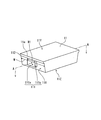
- FIG. 9A is a perspective view schematically showing the electrolytic capacitor 100 according to the embodiment of the present invention.
- 9B is a sectional view taken along line X 1 -X 2 of electrolytic capacitor 100 in FIG. 9A.
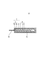
- FIG. 10A and FIG. 10B are diagrams showing the manner of connecting the anode lead terminal 50 and the cathode lead terminal 60 to the capacitor element 10 with the outer package 70 omitted in FIGS. 9A and 9B, respectively.
- 10B is a sectional view taken along line Y 1 -Y 2 of the electrolytic capacitor in FIG. 10A.
- the electrolytic capacitor 100 includes a capacitor element 10 having an anode part 6 and a cathode part 7, an anode lead terminal (anode lead frame) 50 electrically connected to the anode part 6, and a cathode lead electrically connected to the cathode part 7.
- a terminal (cathode lead frame) 60 and an outer package 70 are provided.
- the outer package 70 covers the capacitor element 10 with a part of the anode lead terminal 50 and the cathode lead terminal 60 exposed.
- the anode part 6 has an anode body 1 and an anode wire 2 extending from the anode body 1, and the anode wire 2 is bonded to an anode lead terminal 50.
- the outer surface of the outer package 70 is a first surface A1, a second surface A2 that shares one side with the first surface A1, and a surface that shares one side with the first surface A1 and is opposite to the second surface A2.
- the fourth surface A4 is located on the opposite side of the first surface A1 (see FIG. 9B).
- the anode lead terminal 50 has a first anode lead portion 51, a second anode lead portion 52, and a third anode lead portion 53.
- the third anode lead portion 53 further includes a first region 53a extending in a direction along the first surface A1 (more specifically, a direction along a virtual first plane), and a third region bent from the first region 53a. And a second region 53b extending along the surface A3 (see FIGS. 10A and 10B).
- the anode lead terminal 50 is bent from the first main surface A1 at the first bent portion B1 and the second bent portion B2.
- a part of the anode lead frame 50 is bent in the direction toward the anode wire 2 at the first bent portion B1 to form a second anode lead portion 52.
- Another part of the anode lead terminal 50 is bent along the first surface A1 at the second bent portion B2 to form the third anode lead portion 53.
- the remaining part of the anode lead frame 50 along the second surface A2 constitutes the first anode lead part 51.
- the second anode lead portion 52 is connected to the anode wire 2.
- the entire third anode lead portion 53 is exposed from the outer package 70, and the third anode lead portion 53 covers the first surface A1 in the first region 53a.
- the third anode lead portion 53 covers the first surface A1 in the first region 53a.
- the first bent portion B1 is located closer to the capacitor element 10 side than the second bent portion B2. That is, the second anode lead portion 52 is bent at a position closer to the cathode portion of the capacitor element than the third anode lead portion 53. Due to this, as shown in FIG. 10A, the anode lead terminal 50 has an opening formed on the first surface side.
- the first region 53a exposed from the outer package 70 does not cover the entire first surface, and the region where the anode lead terminal 50 (third anode lead portion 53) is not exposed corresponds to the opening. It exists in the area (third area) on the first surface.
- a protrusion (first protrusion) 71 is provided in a region on the first surface corresponding to the opening, and a first region 53 a extends so as to surround the protrusion 71. There is.
- the anode wire 2 extends toward the protrusion 71 (see FIG. 10A, but the protrusion 71 is not shown in FIG. 10A).
- the cathode lead terminal has a first cathode lead portion 61 and a second cathode lead portion 62.
- a part of the cathode lead terminal 60 is bent along the second surface A2 to the fourth surface A4, the bent portion constitutes the first cathode lead portion 61, and the remaining portion constitutes the second cathode lead portion 62.
- the first cathode lead portion 61 is electrically connected to the cathode portion of the capacitor element 10 on the second surface A2 side via a conductive adhesive (not shown) (for example, silver paste).
- the second cathode lead portion 62 further has a first area 62a extending in the direction along the fourth surface A4 and a second area 62b bent from the first area 62a and extending along the third surface A3. As shown in FIG. 10B, the entire second cathode lead portion 62 including the first region 62a and the second region 62b is exposed from the outer package 70.
- the cathode lead terminal 60 similarly to the anode lead terminal 50, the cathode lead terminal 60 also has an opening formed on the fourth surface A4 side.
- the first region 62a of the cathode lead terminal 60 exposed from the outer package 70 does not cover the entire fourth surface A4, and the region where the cathode lead terminal 60 (second cathode lead portion 62) is not exposed is It exists in the area
- a projecting portion 72 is provided in a region on the fourth surface corresponding to the opening, and a first region 62a is formed so as to surround the projecting portion 72.
- the distance from the second surface A2 where the cathode lead terminal 60 and the cathode part are electrically connected to the capacitor element 10 is usually the outer package. Is smaller than the distance from the third surface A3 to the capacitor element 10 (that is, the thickness of the exterior body covering the third main surface A3 side of the cathode portion). Therefore, from the viewpoint of ensuring insulation between the cathode portion and the anode lead terminal 50, the end portion position L 1 of the first anode lead portion 51 shown in FIG. 10B and the end portion on the first surface side of the cathode portion of the capacitor element. It becomes necessary to provide a certain distance from the position L 2 .
- the area of the first anode lead portion 51 is reduced by providing the second anode lead portion 52.
- the area of the first anode lead portion 51 is limited by the arrangement of the second anode lead portion and the cathode portion, and it has been necessary to devise to expand the land area for connection with the external substrate.
- the first cathode lead part 61 is bent inside the outer package 70 to increase the thickness of the outer package covering the first surface A1 side of the cathode part.
- the thickness of the outer casing is increased, the volume occupied by the capacitor element is reduced and the capacitance is reduced.
- the electrolytic capacitor 100 is electrically connected to the external substrate by the third surface on the side opposite to the second surface A1 on which the cathode lead terminal 60 and the cathode portion are electrically connected. Done on surface A3. Therefore, the shape and area of the third anode lead portion 53 can be set arbitrarily regardless of the arrangement of the cathode portion. As shown in FIG. 10B, the end position L 3 of the third anode lead portion 53 can be set to a position exceeding L 2 and overlapping with the cathode portion. As a result, the area of the third anode lead portion 53 can be increased and the reliability of connection with the external substrate can be improved without reducing the capacitance.
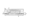
- FIG. 11 is a sectional view schematically showing an example of the capacitor element according to the present embodiment.
- the capacitor element 10 includes an anode part 6 and a cathode part 7.
- the anode part 6 has an anode body 1 having a dielectric layer 3 and an anode wire 2.
- the cathode part 7 has a solid electrolyte layer 4 formed on the dielectric layer 3, and a cathode layer 5 (carbon layer 5a and metal paste layer 5b) that covers the surface of the solid electrolyte layer 4.
- the anode wire 2 has a first portion 2a embedded from one surface (planting surface) of the anode body 1 into the inside of the anode body 1, and a second portion 2b extending from the one surface of the anode body 1.
- the anode part has, for example, an anode body and an anode wire extending from one surface of the anode body and electrically connected to the anode lead terminal.
- the anode body is, for example, a rectangular parallelepiped porous sintered body obtained by sintering metal particles.
- the metal particles particles of valve action metal such as titanium (Ti), tantalum (Ta), niobium (Nb) are used.
- One type or two or more types of metal particles are used for the anode body.
- the metal particles may be an alloy composed of two or more kinds of metals. For example, an alloy containing a valve metal and silicon, vanadium, boron or the like can be used. Alternatively, a compound containing a valve metal and a typical element such as nitrogen may be used.
- the alloy of the valve action metal contains the valve action metal as a main component and contains, for example, 50 atom% or more of the valve action metal.
- the anode wire is made of a conductive material.
- the material for the anode wire is not particularly limited, and examples thereof include copper, aluminum, and aluminum alloys in addition to the above valve action metal.
- the materials forming the anode body and the anode wire may be the same or different.
- the cross-sectional shape of the anode wire is not particularly limited, and examples thereof include a circle, a track shape (a shape including straight lines parallel to each other and two curves connecting the ends of these straight lines), an ellipse, a rectangle, and a polygon. .
- the anode part is produced, for example, by pressure-molding a rectangular parallelepiped in a state where the first part is embedded in the powder of the metal particles and sintering.
- the second portion of the anode wire is pulled out from one surface of the anode body so as to stand.
- the second portion is joined to the anode lead terminal by welding or the like, and the anode wire and the anode lead terminal are electrically connected.
- the welding method is not particularly limited, and examples thereof include resistance welding and laser welding.
- a dielectric layer is formed on the surface of the anode body.
- the dielectric layer is made of, for example, a metal oxide.
- a method of forming a layer containing a metal oxide on the surface of the anode body for example, a method of anodizing the surface of the anode body by dipping the anode body in a chemical conversion solution, or the anode body under an atmosphere containing oxygen. The method of heating is mentioned.
- the dielectric layer is not limited to the layer containing the above metal oxide, and may have an insulating property.
- the cathode part has a solid electrolyte layer formed on the dielectric layer and a cathode layer covering the solid electrolyte layer.
- the solid electrolyte layer may be formed so as to cover at least a part of the dielectric layer.
- a manganese compound or a conductive polymer is used for the solid electrolyte layer.
- the conductive polymer include polypyrrole, polythiophene, polyfuran, polyaniline, polyacetylene, polyphenylene, polyparaphenylenevinylene, polyacene, polythiophenvinylene, polyfluorene, polyvinylcarbazole, polyvinylphenol, polypyridine, and derivatives of these polymers.
- the conductive polymer may be a copolymer of two or more kinds of monomers. It may be polythiophene, polyaniline, or polypyrrole in terms of excellent conductivity. In particular, polypyrrole may be used because it is excellent in water repellency.
- the solid electrolyte layer containing the conductive polymer is formed, for example, by polymerizing raw material monomers on the dielectric layer. Alternatively, it is formed by applying a liquid containing the conductive polymer to the dielectric layer.
- the solid electrolyte layer is composed of one or more solid electrolyte layers. When the solid electrolyte layer is composed of two or more layers, the composition and forming method (polymerization method) of the conductive polymer used in each layer may be different.
- polypyrrole, polythiophene, polyfuran, polyaniline and the like mean polymers having a basic skeleton of polypyrrole, polythiophene, polyfuran, polyaniline and the like, respectively. Therefore, polypyrrole, polythiophene, polyfuran, polyaniline and the like may include their respective derivatives.
- polythiophene includes poly(3,4-ethylenedioxythiophene) and the like.
- various dopants may be added to the polymerization liquid for forming the conductive polymer, the solution or the dispersion liquid of the conductive polymer.
- the dopant is not particularly limited, 1,5-naphthalenedisulfonic acid, 1,6-naphthalenedisulfonic acid, 1-octanesulfonic acid, 1-naphthalenesulfonic acid, 2-naphthalenesulfonic acid, 2,6-naphthalenedisulfonic acid, 2,7-naphthalenedisulfonic acid, 2-methyl-5-isopropylbenzenesulfonic acid, 4-octylbenzenesulfonic acid, 4-nitrotoluene-2-sulfonic acid, m-nitrobenzenesulfonic acid, n-octylsulfonic acid, n-butane Sulfonic acid, n-hexanesulfonic acid, o-nitrobenzenesul
- the derivative examples include metal salts such as lithium salt, potassium salt and sodium salt, ammonium salts such as methylammonium salt, dimethylammonium salt and trimethylammonium salt, piperidinium salt, pyrrolidinium salt and pyrrolinium salt.
- metal salts such as lithium salt, potassium salt and sodium salt
- ammonium salts such as methylammonium salt, dimethylammonium salt and trimethylammonium salt
- piperidinium salt such as pyrrolidinium salt and pyrrolinium salt.
- the average particle diameter D50 of the particles is, for example, 0.01 ⁇ m or more and 0.5 ⁇ m or less. When the average particle diameter D50 of the particles is within this range, the particles easily penetrate into the inside of the anode body.
- the cathode layer has, for example, a carbon layer formed so as to cover the solid electrolyte layer, and a metal paste layer formed on the surface of the carbon layer.
- the carbon layer contains a conductive carbon material such as graphite and a resin.
- the metal paste layer contains, for example, metal particles (for example, silver) and a resin.
- the configuration of the cathode layer is not limited to this configuration.
- the cathode layer may have any structure as long as it has a current collecting function.
- ⁇ Anode lead terminal> One end of the anode lead terminal is joined to the anode wire by a conductive adhesive material, solder, resistance welding or laser welding. The other end of the anode lead terminal is led out from the exterior body. A part of the exposed portion of the anode lead terminal is arranged on either surface of the outer package together with the cathode lead terminal.
- the material of the anode lead terminal is not particularly limited as long as it is electrochemically and chemically stable and has conductivity.
- the anode lead terminal may be a metal such as copper or a nonmetal.
- the shape is not particularly limited as long as it is flat.
- the thickness of the anode lead terminal (the length between the main surfaces of the anode lead terminal) may be 25 ⁇ m or more and 200 ⁇ m or less, or 25 ⁇ m or more and 100 ⁇ m or less from the viewpoint of reducing the height.
- the anode lead terminal may be joined to the anode wire by a conductive adhesive or solder, or may be joined to the anode wire by resistance welding or laser welding.
- the conductive adhesive is, for example, a mixture of a thermosetting resin described below and carbon particles or metal particles.
- the cathode lead terminal is bonded to the cathode layer via, for example, a conductive adhesive material.
- One end of the cathode lead terminal is arranged inside the outer package.
- the other end of the cathode lead terminal is led out from the exterior body.
- a part of the exposed portion of the cathode lead terminal is arranged on either surface of the outer package together with the anode lead terminal.
- the material of the cathode lead terminal is not particularly limited as long as it is electrochemically and chemically stable and has conductivity.
- the cathode lead terminal may be a metal such as copper or a nonmetal.
- the shape is also not particularly limited, and is, for example, long and flat.
- the thickness of the cathode lead terminal may be 25 ⁇ m or more and 200 ⁇ m or less, or 25 ⁇ m or more and 100 ⁇ m or less, from the viewpoint of reducing the height.
- the outer package is provided to electrically insulate the anode lead terminal and the cathode lead terminal, and is made of an insulating material (exterior body material).
- the exterior body material includes, for example, a thermosetting resin.
- the thermosetting resin include epoxy resin, phenol resin, silicone resin, melamine resin, urea resin, alkyd resin, polyurethane, polyimide and unsaturated polyester.
- the electrolytic capacitor includes, for example, a preparation step (S1) of preparing a capacitor element to which an anode lead terminal and a cathode lead terminal are connected, a capacitor element, a part of the anode lead terminal, and a part of the cathode lead terminal. It is manufactured by a method including a sealing step (S2) of forming an outer package to be sealed and a bending step (S3) of bending an exposed portion of the anode lead terminal exposed from the outer package.
- FIG. 12 is a flowchart showing the method of manufacturing the electrolytic capacitor according to the present embodiment.
- the manufacturing method of the electrolytic capacitor according to the present embodiment will be described in detail, taking the case of manufacturing the electrolytic capacitor shown in FIGS. 5 and 6 as an example.
- the exterior body has a second surface and a third surface that share one side with the first surface and that face each other, and the area of the second surface is larger than the area of the third surface.
- the first surface, the second surface, and the third surface each have a flat surface portion, and an angle ⁇ 1 formed by the flat surface portion of the first surface and the flat surface portion of the second surface is less than 90 degrees.
- the first projecting portion shares the first surface on the second surface side of the first surface with the first surface, and the angle ⁇ 2 formed by the second surface flat portion is larger than the angle ⁇ 1 and 90 degrees or less. Is formed in a virtual space R formed by a virtual first plane and a virtual third plane that is on the same plane as the plane portion of the third surface.
- the first protruding portion includes a protruding surface and a plurality of rising surfaces that connect the protruding surface and the first surface, and the protruding surface is on the same plane as the virtual first surface.
- the manufacturing method according to the present embodiment is useful when the outer shape of the exterior body is tapered and the exterior body has the first protruding portion.
- a capacitor element is prepared.
- the valve action metal particles and the anode wire are put into a mold so that the first part is embedded in the valve action metal particles, pressure-molded, and then sintered in a vacuum, whereby the first part is made of a porous sintered body.
- An anode part to be embedded inside is prepared from one surface.
- the pressure at the time of pressure molding is not particularly limited and is, for example, about 10 N or more and 100 N or less.
- the valve action metal particles may be mixed with a binder such as polyacrylic carbonate, if necessary.
- a dielectric layer is formed on the anode body.
- the anode body is immersed in a chemical conversion tank filled with an electrolytic aqueous solution (for example, phosphoric acid aqueous solution), and the second portion of the anode wire is connected to the anode body of the chemical conversion tank to perform anodization.
- an electrolytic aqueous solution for example, phosphoric acid aqueous solution
- the dielectric layer made of the oxide film of the valve metal can be formed on the surface of the anode body.
- the electrolytic aqueous solution is not limited to the phosphoric acid aqueous solution, and nitric acid, acetic acid, sulfuric acid or the like can be used.
- the solid electrolyte layer containing a conductive polymer is, for example, a method of impregnating an anode body on which a dielectric layer is formed with a monomer or oligomer, and then polymerizing the monomer or oligomer by chemical polymerization or electrolytic polymerization, or The anode body on which the body layer is formed is impregnated with a solution or dispersion of a conductive polymer and dried to form at least a part of the dielectric layer.
- a carbon paste and a metal paste are sequentially applied to the surface of the solid electrolyte layer to form a cathode layer composed of the carbon layer and the metal paste layer.
- the structure of the cathode layer is not limited to this, and may be any structure having a current collecting function.
- the capacitor element is manufactured by the above method.
- the anode lead terminal and the cathode lead terminal are prepared and joined to the capacitor element.
- a bent portion (internal bent portion) arranged inside the outer package is formed on the anode lead terminal.
- the internal bent portion is formed by, for example, press working.
- the position of the internal bent portion of the anode lead terminal is appropriately set according to the length and diameter of the anode wire.
- An internal bent portion may be formed also in the cathode lead terminal.
- the capacitor element Place the capacitor element with each lead terminal placed.
- the second portion of the anode wire and the vicinity of one end of the anode lead terminal are joined by laser welding or resistance welding.
- the vicinity of one end of the cathode lead terminal is joined to the cathode layer via a conductive adhesive.
- FIG. 13A is a cross-sectional view schematically showing the capacitor element to which the lead terminals prepared in the preparation step of the manufacturing method according to the present embodiment are joined.
- the capacitor element 10 includes the anode wire 2 that is planted from the planting surface 1X.
- An anode lead terminal 13 is joined to the anode wire 2 (second portion 2b).
- a cathode lead terminal 14 is joined to the cathode portion of the capacitor element 10.
- a bent portion corresponding to the inner bent portion is formed in the anode lead terminal 13.
- the materials of the capacitor element and the outer casing are placed in a mold, and the capacitor element is sealed by a transfer molding method, a compression molding method, or the like. At this time, a part of the anode lead terminal and the cathode lead terminal is led out from the mold.
- the molding conditions are not particularly limited, and the time and temperature conditions may be appropriately set in consideration of the curing temperature of the thermosetting resin used.
- FIG. 13B is a sectional view schematically showing the mold and the capacitor element housed in the mold in the sealing step of the manufacturing method according to the present embodiment.
- the capacitor element 10 is housed in the mold 30 together with the outer package material 11P. A part of the anode lead terminal 13 and the cathode lead terminal 14 is led out from the mold 30.
- the mold 30 includes a deep first mold 31 that can accommodate the capacitor element 10 and a second mold 32 that has a shallow step.
- the first mold 31 is formed with a recess 31a for forming the first protrusion.
- the bottom surface of the first mold 31 is narrower than the area of the opening, and the first mold 31 has a tapered shape.
- the first mold 31 and the second mold 32 are fitted to each other to form the container-shaped mold 30.
- the anode lead terminal 13 and the cathode lead terminal 14 are led out to the outside through a gap generated when the first die 31 and the second die 32 are fitted together.
- an electrolytic capacitor including a capacitor element, an anode lead terminal, a cathode lead terminal, and an exterior body that covers a part of the capacitor element and each lead terminal can be obtained.
- FIG. 13C is a sectional view schematically showing how the first mold is released in the sealing step of the manufacturing method according to the present embodiment.
- the capacitor element 10 is taken out, for example, the second mold 32 is fixed and the first mold 31 is moved in a direction in which it is separated from the capacitor element 10.
- the anode lead terminal is bent along the virtual first plane (see FIG. 4).
- the first projecting portion formed on the side surface of the exterior body may be used as a guide.
- the anode lead terminal is bent by moving the bending roller from the second surface toward the third surface of the exterior body while pressing the bending roller against the first protrusion. In this case, since the bending roller is stably moved, the bending accuracy is improved.
- FIG. 13D is a sectional view schematically showing how the anode lead terminal is bent in the bending step of the manufacturing method according to the present embodiment.
- the bending roller 40 moves from the second surface (flat surface portion 11Y) of the exterior body 11 toward the third surface (flat surface portion 11Z) while being guided by the first protruding portion 111.
- the anode lead terminal 13 is pressed by the bending roller 40 and bent in a shape along the imaginary first plane.
- the protruding surface of the first protruding portion 111 and the outer surface 13X of the anode lead terminal 13 are both on the same plane as the virtual first plane 11Xv.
- the anode lead terminal 13 is then further bent along the third surface.
- the cathode lead terminal 14 may be bent by using a bending roller.
- the anode lead terminal (anode lead frame) 50 shown in FIG. 14 may be used in the preparation process. As a result, the electrolytic capacitor 100 shown in FIG. 9A can be manufactured.
- a U-shaped cut C is formed along the contour line of the formation region (for example, a rectangular region) of the second anode lead portion 52, except for one straight side of the contour line. (Dashed line part) is formed.
- the punching of the anode lead terminal 50 and the formation of the cut may be performed at the same time.
- the portion in which the cut is not formed is the first bent portion B1. It should be noted that in FIG. 14, the alternate long and short dash line is the portion that serves as the axis of the bending process.
- the cut length U may be longer than the height of the anode wire 2 from the second surface A2.
- the anode lead terminal (third anode lead portion) is arranged around the first projecting portion of the outer package, and the anode lead terminal does not cover the first projecting portion. 50 may form a through hole 54 adjacent to the notch.
- the formation region of the second anode lead portion 52 is bent around the first bent portion B1 as an axis, and the second anode lead portion 52 is erected from the anode lead frame.
- the bent portion is formed by bending, for example.
- the position of the first bent portion B1 may be appropriately set according to the size of the capacitor element and the like (in particular, the position of the extending portion of the anode wire 2 in the capacitor element).
- the anode lead terminal 50 is bent from the direction along the second surface A2 to the direction along the first surface A1, and further from the direction along the first surface A1 to the third surface A3 facing the second surface A2. It is bent along the direction.
- the cathode lead terminal is bent from the direction along the second surface A2 to the direction along the fourth surface A4, and further from the direction along the fourth surface A4 along the third surface A3 facing the second surface A2. To be bent.
- the boundary between the portion along the first main surface A1 and the portion along the second main surface A2 is the second bent portion B2.
- a part of the anode lead terminal 50 extending in a direction away from the outer package 70 forms a third anode lead portion 53 with the second bent portion B2 as a reference.
- the portion excluding the second anode lead portion 52 constitutes the first anode lead portion 51.
- the cathode lead terminal 60 a part of the cathode lead terminal 60 extending in a direction away from the outer package 70 with reference to a boundary between a portion along the first main surface A1 and a portion along the fourth main surface A4. Constitutes the second cathode lead portion 62, and the remaining portion constitutes the first cathode lead portion 61.
- the electrolytic capacitor according to the present invention can be used in various applications because the size of the capacitor element can be increased. While the present invention has been described in terms of its presently preferred embodiments, such disclosure should not be construed as limiting. Various variations and modifications will no doubt become apparent to those skilled in the art to which the present invention pertains upon reading the above disclosure. Therefore, the appended claims should be construed to cover all variations and modifications without departing from the true spirit and scope of the present invention.
- Electrolytic capacitor 10 Capacitor element 1: Anode body 1X: Embedding surface 2: Anode wire 2a: First part 2b: Second part 3: Dielectric layer 4: Solid electrolyte layer 5: Cathode layer 5a: Carbon layer 5b: Metal paste layer 6: Anode part 7: Cathode part 8: Conductive adhesive material 11, 70: Outer package A1: First surface A2: Second surface A3: Third surface A4: Fourth surface 11X: First surface (Flat part) 11Y: Second surface (flat surface portion) 11Z: Third surface (flat surface portion) 11Xv: Virtual 1st plane 11Zv: Virtual 3rd plane 11a: 1st side 111: 1st protrusion part 111x: Protrusion surface 111y, 111z: Rising surface 112: 2nd protrusion part 11P: Material 71, 72 of an exterior body.
Landscapes
- Engineering & Computer Science (AREA)
- Power Engineering (AREA)
- Microelectronics & Electronic Packaging (AREA)
- Fixed Capacitors And Capacitor Manufacturing Machines (AREA)
- Electric Double-Layer Capacitors Or The Like (AREA)
- Chemical & Material Sciences (AREA)
- Chemical Kinetics & Catalysis (AREA)
- Electrochemistry (AREA)
- Manufacturing & Machinery (AREA)
Abstract
L'invention concerne un condensateur électrolytique comprenant : un élément condensateur comportant une partie électrode positive et une partie électrode négative ; une borne de conducteur d'électrode positive électriquement connectée à la partie électrode positive ; une borne de conducteur d'électrode négative électriquement connectée à la partie électrode négative ; et un corps extérieur qui recouvre l'élément condensateur, la partie électrode positive comportant un corps d'électrode positive et un fil d'électrode positive s'étendant d'une surface d'implantation du corps d'électrode positive vers l'extérieur du corps d'électrode positive, le corps extérieur comportant une première surface orientée vers la surface d'implantation, et une deuxième surface et une troisième surface partageant un côté avec la première surface et se faisant face, la superficie de la deuxième surface étant plus grande que la superfice de la troisième surface, un angle θ1 entre la première surface et la deuxième surface étant inférieur à 90 degrés, et la première surface comprenant une partie en saillie située sur un prolongement du fil d'électrode positive et faisant saillie vers l'extérieur du corps extérieur.
Priority Applications (2)
| Application Number | Priority Date | Filing Date | Title |
|---|---|---|---|
| JP2020557888A JPWO2020111278A1 (ja) | 2018-11-30 | 2019-11-29 | 電解コンデンサおよびその製造方法 |
| US17/298,438 US20220028622A1 (en) | 2018-11-30 | 2019-11-29 | Electrolytic capacitor and method for producing the same |
Applications Claiming Priority (4)
| Application Number | Priority Date | Filing Date | Title |
|---|---|---|---|
| JP2018-225595 | 2018-11-30 | ||
| JP2018225594 | 2018-11-30 | ||
| JP2018225595 | 2018-11-30 | ||
| JP2018-225594 | 2018-11-30 |
Publications (1)
| Publication Number | Publication Date |
|---|---|
| WO2020111278A1 true WO2020111278A1 (fr) | 2020-06-04 |
Family
ID=70852808
Family Applications (1)
| Application Number | Title | Priority Date | Filing Date |
|---|---|---|---|
| PCT/JP2019/046924 WO2020111278A1 (fr) | 2018-11-30 | 2019-11-29 | Condensateur électrolytique et son procédé de fabrication |
Country Status (3)
| Country | Link |
|---|---|
| US (1) | US20220028622A1 (fr) |
| JP (1) | JPWO2020111278A1 (fr) |
| WO (1) | WO2020111278A1 (fr) |
Citations (8)
| Publication number | Priority date | Publication date | Assignee | Title |
|---|---|---|---|---|
| JPS59131144U (ja) * | 1983-02-22 | 1984-09-03 | 日本電気株式会社 | チツプ型固体電解コンデンサ |
| JPH0361324U (fr) * | 1989-10-17 | 1991-06-17 | ||
| JPH0722280A (ja) * | 1993-06-16 | 1995-01-24 | Showa Denko Kk | チップ状固体電解コンデンサ |
| JPH0992575A (ja) * | 1995-07-18 | 1997-04-04 | Nec Toyama Ltd | チップ型固体電解コンデンサ |
| JPH10149953A (ja) * | 1996-11-19 | 1998-06-02 | Nec Corp | チップ型電子部品 |
| JPH11288844A (ja) * | 1998-04-03 | 1999-10-19 | Matsuo Electric Co Ltd | 樹脂封止型電子部品及びその製造方法 |
| JP2001291641A (ja) * | 2000-04-07 | 2001-10-19 | Nec Corp | チップ型コンデンサ及びその製造方法並びにモールド金型 |
| JP2006344775A (ja) * | 2005-06-09 | 2006-12-21 | Rohm Co Ltd | パッケージ型固体電解コンデンサ及びその製造方法 |
Family Cites Families (11)
| Publication number | Priority date | Publication date | Assignee | Title |
|---|---|---|---|---|
| JPS6151752U (fr) * | 1984-09-10 | 1986-04-07 | ||
| JPS60220922A (ja) * | 1985-04-01 | 1985-11-05 | 日立エーアイシー株式会社 | チツプ型コンデンサ |
| JPH01230218A (ja) * | 1988-03-10 | 1989-09-13 | Matsuo Denki Kk | 固体電解コンデンサの端子の処理方法 |
| JPH03212920A (ja) * | 1990-01-18 | 1991-09-18 | Elna Co Ltd | 固体電解コンデンサおよびそのユニット |
| JP3187106B2 (ja) * | 1991-12-27 | 2001-07-11 | ローム株式会社 | 電気回路素子のパッケージ構造 |
| JP3117828B2 (ja) * | 1992-12-28 | 2000-12-18 | ローム株式会社 | 合成樹脂封止型電子部品及びそのリード端子の曲げ加工方法 |
| JPH0722289A (ja) * | 1993-07-01 | 1995-01-24 | Hitachi Aic Inc | 固体電解コンデンサ |
| JP2546977B2 (ja) * | 1994-07-29 | 1996-10-23 | 九州日本電気株式会社 | リード成形金型 |
| JP3819728B2 (ja) * | 2001-04-13 | 2006-09-13 | 三洋電機株式会社 | リードフレームを具えた電子部品 |
| JP4656573B2 (ja) * | 2005-12-08 | 2011-03-23 | ニチコン株式会社 | チップ型固体電解コンデンサ |
| JP6295433B2 (ja) * | 2012-08-29 | 2018-03-20 | パナソニックIpマネジメント株式会社 | 固体電解コンデンサ |
-
2019
- 2019-11-29 US US17/298,438 patent/US20220028622A1/en active Pending
- 2019-11-29 JP JP2020557888A patent/JPWO2020111278A1/ja active Pending
- 2019-11-29 WO PCT/JP2019/046924 patent/WO2020111278A1/fr active Application Filing
Patent Citations (8)
| Publication number | Priority date | Publication date | Assignee | Title |
|---|---|---|---|---|
| JPS59131144U (ja) * | 1983-02-22 | 1984-09-03 | 日本電気株式会社 | チツプ型固体電解コンデンサ |
| JPH0361324U (fr) * | 1989-10-17 | 1991-06-17 | ||
| JPH0722280A (ja) * | 1993-06-16 | 1995-01-24 | Showa Denko Kk | チップ状固体電解コンデンサ |
| JPH0992575A (ja) * | 1995-07-18 | 1997-04-04 | Nec Toyama Ltd | チップ型固体電解コンデンサ |
| JPH10149953A (ja) * | 1996-11-19 | 1998-06-02 | Nec Corp | チップ型電子部品 |
| JPH11288844A (ja) * | 1998-04-03 | 1999-10-19 | Matsuo Electric Co Ltd | 樹脂封止型電子部品及びその製造方法 |
| JP2001291641A (ja) * | 2000-04-07 | 2001-10-19 | Nec Corp | チップ型コンデンサ及びその製造方法並びにモールド金型 |
| JP2006344775A (ja) * | 2005-06-09 | 2006-12-21 | Rohm Co Ltd | パッケージ型固体電解コンデンサ及びその製造方法 |
Also Published As
| Publication number | Publication date |
|---|---|
| JPWO2020111278A1 (ja) | 2021-10-14 |
| US20220028622A1 (en) | 2022-01-27 |
Similar Documents
| Publication | Publication Date | Title |
|---|---|---|
| US10347431B2 (en) | Solid electrolytic capacitor with porous sintered body as an anode body and manufacturing thereof | |
| WO2003077268A1 (fr) | Condensateur electrolytique solide | |
| TW200306594A (en) | Solid electrolytic capacitor and manufacturing method therefor | |
| US11201016B2 (en) | Electrolytic capacitor | |
| US8559165B2 (en) | Solid electrolytic capacitor | |
| WO2018123525A1 (fr) | Condensateur électrolytique | |
| US20220399169A1 (en) | Electrolytic capacitor | |
| JP7029670B2 (ja) | 電解コンデンサ | |
| WO2020111278A1 (fr) | Condensateur électrolytique et son procédé de fabrication | |
| JP2018142668A (ja) | 固体電解コンデンサ | |
| WO2018159426A1 (fr) | Condensateur électrolytique | |
| US11984271B2 (en) | Electrolytic capacitor having reduced equivalent series resistance | |
| JP2019145696A (ja) | 電解コンデンサ | |
| US20220319778A1 (en) | Electrolytic capacitor | |
| JP2019067922A (ja) | 電解コンデンサ | |
| WO2023074376A1 (fr) | Condensateur électrolytique solide | |
| US20240006128A1 (en) | Electrolytic capacitor | |
| JP2020072186A (ja) | 電解コンデンサ | |
| JP6913875B2 (ja) | 電解コンデンサ | |
| JP7029666B2 (ja) | 固体電解コンデンサ | |
| JP2020072185A (ja) | 電解コンデンサ | |
| WO2023153177A1 (fr) | Condensateur électrolytique | |
| US20240029962A1 (en) | Electrolytic capacitor | |
| JP2020088342A (ja) | 電解コンデンサ | |
| US20230113070A1 (en) | Electrolytic capacitor |
Legal Events
| Date | Code | Title | Description |
|---|---|---|---|
| 121 | Ep: the epo has been informed by wipo that ep was designated in this application |
Ref document number: 19888353 Country of ref document: EP Kind code of ref document: A1 |
|
| ENP | Entry into the national phase |
Ref document number: 2020557888 Country of ref document: JP Kind code of ref document: A |
|
| NENP | Non-entry into the national phase |
Ref country code: DE |
|
| 122 | Ep: pct application non-entry in european phase |
Ref document number: 19888353 Country of ref document: EP Kind code of ref document: A1 |