WO2020111278A1 - Electrolytic capacitor and method of manufacturing same - Google Patents
Electrolytic capacitor and method of manufacturing same Download PDFInfo
- Publication number
- WO2020111278A1 WO2020111278A1 PCT/JP2019/046924 JP2019046924W WO2020111278A1 WO 2020111278 A1 WO2020111278 A1 WO 2020111278A1 JP 2019046924 W JP2019046924 W JP 2019046924W WO 2020111278 A1 WO2020111278 A1 WO 2020111278A1
- Authority
- WO
- WIPO (PCT)
- Prior art keywords
- anode
- anode lead
- lead terminal
- cathode
- plane
- Prior art date
Links
Images


Classifications
-
- H—ELECTRICITY
- H01—ELECTRIC ELEMENTS
- H01G—CAPACITORS; CAPACITORS, RECTIFIERS, DETECTORS, SWITCHING DEVICES OR LIGHT-SENSITIVE DEVICES, OF THE ELECTROLYTIC TYPE
- H01G9/00—Electrolytic capacitors, rectifiers, detectors, switching devices, light-sensitive or temperature-sensitive devices; Processes of their manufacture
- H01G9/004—Details
- H01G9/08—Housing; Encapsulation
-
- H—ELECTRICITY
- H01—ELECTRIC ELEMENTS
- H01G—CAPACITORS; CAPACITORS, RECTIFIERS, DETECTORS, SWITCHING DEVICES OR LIGHT-SENSITIVE DEVICES, OF THE ELECTROLYTIC TYPE
- H01G9/00—Electrolytic capacitors, rectifiers, detectors, switching devices, light-sensitive or temperature-sensitive devices; Processes of their manufacture
- H01G9/004—Details
- H01G9/008—Terminals
- H01G9/012—Terminals specially adapted for solid capacitors
-
- H—ELECTRICITY
- H01—ELECTRIC ELEMENTS
- H01G—CAPACITORS; CAPACITORS, RECTIFIERS, DETECTORS, SWITCHING DEVICES OR LIGHT-SENSITIVE DEVICES, OF THE ELECTROLYTIC TYPE
- H01G9/00—Electrolytic capacitors, rectifiers, detectors, switching devices, light-sensitive or temperature-sensitive devices; Processes of their manufacture
- H01G9/15—Solid electrolytic capacitors
Definitions
- the present invention relates to an electrolytic capacitor and a method for manufacturing the same.
- Electrolytic capacitors have a small equivalent series resistance (ESR) and excellent frequency characteristics, so they are used in various electronic devices.
- the electrolytic capacitor includes a capacitor element having an anode part and a cathode part, an anode lead terminal electrically connected to the anode part, and a cathode lead terminal electrically connected to the cathode part.
- the capacitor element is usually sealed with an exterior body.
- the encapsulation of the capacitor element is performed by, for example, a transfer molding method, a compression molding method, etc., in which the materials of the capacitor element and the outer casing (uncured thermosetting resin and filler) are housed in a mold.
- the side surface of the exterior body is designed in a tapered shape in consideration of the mold releasability (see Patent Document 1).
- electrolytic capacitors are required to have high capacity and small size.
- its volume is smaller than that of the rectangular parallelepiped exterior body, so that the capacitor element that can be sealed is also small.
- a first aspect of the present invention a capacitor element having an anode portion and a cathode portion, an anode lead terminal electrically connected to the anode portion, a cathode lead terminal electrically connected to the cathode portion, An exterior body covering the capacitor element, wherein the anode part has an anode body and an anode wire extending from the erected surface of the anode body toward the outside of the anode body.
- a second aspect of the present invention is a preparation step of preparing a capacitor element to which an anode lead terminal and a cathode lead terminal are connected, the capacitor element, a part of the anode lead terminal, and a part of the cathode lead terminal. And a bending step of bending an exposed portion of the anode lead terminal exposed from the outer package, and a sealing step of forming an outer package that seals
- the first surface includes a protrusion that protrudes to the outside of the exterior body, and in the bending step, the exposed portion of the anode lead terminal is bent by a roller that moves along the protrusion. Manufacturing method.
- the size of the capacitor element can be increased.
- FIG. 3 is a cross-sectional view of the exterior body taken along the line AA of FIG. 2. It is sectional drawing which expands and shows the principal part in the AA line of the exterior body of FIG. It is a perspective view which shows typically the electrolytic capacitor which concerns on one Embodiment of this invention.
- FIG. 6 is a sectional view taken along line BB of the electrolytic capacitor of FIG. 5. It is a perspective view which shows typically the electrolytic capacitor which concerns on other embodiment of this invention.
- FIG. 8 is a sectional view of the electrolytic capacitor taken along the line CC of FIG. 7. It is a perspective view which shows typically the electrolytic capacitor which concerns on other embodiment of this invention.
- FIG. 9B is a cross-sectional view taken along line X 1 -X 2 of the electrolytic capacitor of FIG. 9A.
- FIG. 9A is a perspective view showing a state of connection of the anode lead terminal and the cathode lead terminal to the capacitor element, with the illustration of the outer casing omitted in FIG. 9A.
- FIG. 10B is a cross-sectional view taken along line Y 1 -Y 2 of the electrolytic capacitor of FIG. 10A. It is a sectional view showing the capacitor element concerning one embodiment of the present invention typically.
- FIG. 6 is a flowchart showing a method for manufacturing an electrolytic capacitor according to an embodiment of the present invention.
- FIG. 6 is a cross-sectional view schematically showing a capacitor element to which each lead terminal prepared in the preparation step of the manufacturing method according to the embodiment of the present invention is joined.
- FIG. 6 is a cross-sectional view schematically showing a mold and a capacitor element housed in the mold in a sealing step of the manufacturing method according to the embodiment of the present invention. It is sectional drawing which shows typically a mode that a 1st metal mold is released in the sealing process of the manufacturing method which concerns on one Embodiment of this invention.
- FIG. 6 is a flowchart showing a method for manufacturing an electrolytic capacitor according to an embodiment of the present invention.
- FIG. 6 is a cross-sectional view schematically showing a capacitor element to which each lead terminal prepared in the preparation step of the manufacturing method according to the embodiment of the present invention is joined.
- FIG. 6 is a cross-sectional view schematically showing a
- FIG. 6 is a cross-sectional view schematically showing how the anode lead terminal is bent in the bending step of the manufacturing method according to the embodiment of the present invention.
- FIG. 3 is a schematic view of an anode lead terminal (lead frame) used in manufacturing the electrolytic capacitor according to the embodiment of the present invention. It is sectional drawing which shows the conventional exterior body typically.
- the outer dimensions of electrolytic capacitors are usually strictly defined. Therefore, in order to increase the capacity, it is necessary to increase the size of the sealed capacitor element without changing the outer dimensions of the electrolytic capacitor.
- FIG. 15 is sectional drawing which shows the conventional exterior body typically.
- the capacitor element 210 includes an anode wire 202 that is electrically connected to the anode body and that is erected from one surface (planting surface) of the anode body.
- an anode wire 202 is secured between the anode wire 202 and the side surface 211X of the exterior body 211 which is an extension of the anode wire 202.
- an anode lead terminal (not shown) is joined to the anode wire 202.
- the length L2 of the portion where the anode wire 202 is erected needs to be a certain length or more.
- the length L211 of the exterior body 211 around the anode wire 202 in the longitudinal direction A of the anode wire 202 is smaller than the design value L in the longitudinal direction A of the electrolytic capacitor. It becomes shorter by at least the length L3. That is, the size of the capacitor element 210 must be determined in consideration of the shortened L3 in addition to the length L1 and the length L2. Therefore, the length in the longitudinal direction A of the capacitor element 210 becomes smaller than the design value L.
- a protrusion is provided on one surface (first surface) on the extension of the anode wire of the outer package to supplement at least part of L3 shortened by the taper.
- the length of the anode wire in the longitudinal direction A of the outer package approaches the design value L. Therefore, the length in the longitudinal direction A of the capacitor element can be increased while securing the length L1 and the length L2.
- the protruding portion is provided on the first surface, since the taper shape is maintained on the other portions of the first surface, the mold releasability of the mold is not easily impaired.
- the electrolytic capacitor according to the present embodiment is a capacitor element including an anode part and a cathode part, an anode lead terminal electrically connected to the anode part, and a cathode lead terminal electrically connected to the cathode part, And an exterior body that covers the capacitor element.
- the anode part has an anode body and an anode wire extending from the planting surface of the anode body toward the outside of the anode body.
- the exterior body has a first surface that faces the planting surface, and a second surface and a third surface that share one side with the first surface and that face each other.
- the first surface, the second surface, and the third surface each have a flat surface portion.
- the area of the second surface is larger than the area of the third surface.
- the angle ⁇ 1 formed by the flat portion of the first surface and the flat portion of the second surface is less than 90 degrees.
- the first surface is provided on the extension of the anode wire and includes a protrusion that protrudes to
- the area of the second surface is larger than the area of the third surface, for example, 102% or more of the third area, and 105% or more.
- the area of the second surface may be 120% or less of the area of the third surface, and may be 115% or less.
- the area in this case is not the surface area, but the projected area when viewed from the normal direction of the second surface or the third surface (usually the projected area when viewed from the upper surface or the lower surface of the electrolytic capacitor).
- the first to third surfaces of the exterior body usually mean three of the six main surfaces of the outer surface of the exterior body formed to have a substantially rectangular parallelepiped shape.
- the outer surface of the outer package may also have a fourth surface that shares one side with each of the second surface and the third surface and that is located opposite to the first surface.
- the first to fourth surfaces usually refer to four main surfaces of the substantially rectangular parallelepiped except for the two surfaces facing each other. These first to fourth surfaces have a flat surface portion, and the angle formed by the two surfaces of the exterior body can be defined by the angle formed by the flat surface portions.
- each of the first to fourth surfaces has a curved surface portion, includes some irregularities, and/or is formed by a plurality of curved flat surfaces, as long as it has a flat surface portion. You may.
- the first surface to the fourth surface may have a plurality of flat portions. In that case, the angle formed by the planes is defined using the flat surface portion having the largest area among the plurality of flat surface portions.
- the first surface of the exterior body has a plurality of flat portions 11X, 111x and 112 (and a flat portion connecting 11X and 112).
- the angle ⁇ 1 formed by the flat surface portion of the first surface and the flat surface portion of the second surface is defined by the angle formed by the flat surface portion 11X having the largest area of the first surface and the flat surface portion 11Y of the second surface. ..
- the angle formed by the first surface and the second surface is smaller than 90 degrees.
- the angle ⁇ 1 formed by the flat portion of the first surface and the flat portion of the second surface is not particularly limited as long as it is less than 90 degrees, and the mold releasability and the size of the capacitor element to be sealed are taken into consideration. Is set appropriately.
- the angle ⁇ 1 may be 89 degrees or less and may be 88 degrees or less, for example.
- the angle ⁇ 1 may be, for example, 80 degrees or more, and may be 83 degrees or more.
- the protrusion has, for example, an imaginary first plane whose angle ⁇ 2 formed by the plane portion of the second surface is greater than the angle ⁇ 1 and 90 degrees or less, and an imaginary third plane which is coplanar with the plane portion of the third surface. Assuming a plane, it is formed in a virtual space between the virtual first plane, the virtual third plane, and the plane portion of the actual first plane.
- the angle ⁇ 2 is not particularly limited as long as it is larger than the angle ⁇ 1 and 90 degrees or less.
- the angle ⁇ 2 may be set so that the angle ⁇ 3 formed by the virtual first plane and the virtual third plane is 90 degrees or more.
- the angle ⁇ 3 is smaller than 90 degrees, the mold releasability of the mold is likely to be impaired.
- the angle ⁇ 2 may be specifically less than 90 degrees and may be 89 degrees or less.
- the angle ⁇ 2 may be greater than 80 degrees and greater than 83 degrees.
- the electrolytic capacitor according to the present embodiment is, in another non-limiting embodiment, a capacitor element including an anode part and a cathode part, an anode lead terminal electrically connected to the anode part, and an electric connection to the cathode part.
- a cathode lead terminal and an outer package are provided.
- the exterior body has a first surface and a second surface and a third surface that share one side with the first surface and face each other. The exterior body covers the capacitor element with a part of the anode lead terminal and the cathode lead terminal exposed.
- the anode lead terminal includes a first anode lead portion extending along the second surface, a second anode lead portion rising from the first anode lead portion and contacting the anode portion, and extending from the first anode lead portion along the first surface. And a third anode lead portion that further extends along the third surface and is exposed from the outer package on at least the third surface.
- a first bent portion may be formed at a boundary between the first anode lead portion and the second anode lead portion, and a second bent portion may be formed at a boundary between the first anode lead portion and the third anode lead portion. The first bent portion is located closer to the capacitor element than the second bent portion when viewed in a direction perpendicular to the flat portion of the second surface.
- the fact that the first bent portion is located closer to the capacitor element side than the second bent portion means that when the electrolytic capacitor is viewed from a direction perpendicular to the plane portion of the second surface, the first bent portion is a cathode portion of the capacitor element. Is shorter than the distance from the second bent portion to the cathode portion of the capacitor element.
- the cathode lead terminal usually has a first cathode lead portion arranged along the second surface and electrically connected to the cathode portion.
- the cathode lead terminal further extends from the first cathode lead portion along a fourth surface which shares one side with each of the second surface and the third surface and is an outer surface of the outer package opposite to the first surface.
- a second cathode lead portion that extends along the third surface and is exposed from the outer package on at least the third surface may be provided.
- the anode or cathode lead terminal extending along the first to fourth surfaces or the plane portion thereof is not limited to the case where the lead terminal extends parallel to each surface while maintaining a constant distance.
- the lead terminal extends while bending along the unevenness.
- the portion of the third anode lead portion extending along the first surface may extend in a direction substantially parallel to the virtual first plane.
- the anode lead terminal may integrally have a first anode lead portion, a second anode lead portion, and a third anode lead portion.
- the anode lead terminal is bent and bent, and the anode lead terminal is connected to the anode portion via the second anode lead portion.
- at least a part of the third anode lead portion is exposed from the exterior body. As a result, it is possible to connect to the external substrate via the third anode lead portion.
- the first anode lead portion is arranged along the second surface of the outer package, and the second anode lead portion is bent in the direction from the direction along the second surface toward the anode portion and contacts the anode portion.
- the electrical connection between the anode lead terminal and the anode part can be made by the second anode lead part.
- the direction toward the anode part is usually a direction along the first surface and/or a direction intersecting with the second surface, but a direction inclined to the first surface and the second surface. It may be.
- a method of connecting the anode part and the anode lead terminal As a method of connecting the anode part and the anode lead terminal, a method is known in which a cut is made in the anode lead frame, a part of the anode lead frame is raised, and the anode part is brought into contact with the anode part (for example, Japanese Patent Laid-Open No. 2001-126958). Japanese Patent Laid-Open No. 2005-088718).
- the electrical connection between the anode of the electrolytic capacitor and the external substrate is performed via the first anode lead portion provided on the second surface side, and the electrical connection between the cathode of the electrolytic capacitor and the external substrate is also Similarly, it is performed through the first cathode lead portion provided on the second surface side.
- the thickness of the outer casing that covers the first main surface side of the cathode portion is thin, it is necessary to secure the insulation between the first anode lead portion and the cathode portion. It is difficult to extend to the side toward the cathode part, and it is difficult to expand the area of the first anode lead part. This problem is remarkable when the structure in which a part of the anode lead frame is raised and used for contact with the anode part is adopted, since the area of the first anode lead part is further reduced by the area of the rising part. is there.
- the remaining portion of the anode lead terminal after the second anode lead portion is raised is bent along the outer surface of the outer package to form the second surface.
- a third anode lead portion is arranged on the opposite third surface.
- the anode of the electrolytic capacitor and the external substrate can be electrically connected via the third anode lead portion.
- the shape and area of the third anode lead portion arranged on the third surface are not restricted by the second anode lead portion that contacts the anode portion. Further, it can be arbitrarily set without being restricted by the arrangement, shape and size of the cathode portion of the capacitor element. Therefore, the connection reliability with the external substrate is improved. It is also possible to extend the third anode lead portion along the third surface beyond the position of the end portion on the first surface side of the cathode portion when viewed from the direction perpendicular to the second surface.
- the anode lead terminal in the contour line of the formation region of the second anode lead portion of the anode lead terminal, a cut is made in a portion excluding the first bent portion, and the first bent portion is formed. It is formed by bending the second anode lead portion as an axis and standing it upright from the first main surface.
- the anode lead terminal may have a region (opening) on the second surface where the anode lead terminal does not extend due to the rise of the second anode lead portion.
- the anode lead terminal is bent along the first surface in the same direction as the second anode lead portion with the second bend portion separated from the first bend portion as an axis to form the third anode lead portion.
- the third anode lead portion is further bent at a predetermined position along the first surface to the third surface.
- the third anode lead portion is, for example, a first region that bends from the first anode lead portion and extends in a direction along the plane portion of the first surface, and a second region that bends from the first region and extends along the third surface. And a region.
- the third anode lead portion is constituted by the remaining portion of the anode lead terminal after the second anode lead portion is bent and formed.
- the third anode lead portion and the outer package are provided on the first surface in correspondence with the opening.
- the portion where the first region extends and the first region does not extend A portion where only the outer package exists (hereinafter, referred to as “third region”) may exist.
- the third region may be a protruding portion that protrudes outward from the flat surface portion of the first surface.
- the first region of the third anode lead portion may be provided around the protrusion and exposed from the exterior body.
- the anode part when the anode part is connected to the second anode lead part using an anode part having an anode body and an anode wire extending from the erected face of the anode body, one surface of the exterior body is the erected face. And the anode wire extends toward the first surface inside the outer package. At this time, the anode wire can be arranged so as to extend toward the third region where the anode lead terminal does not extend.
- the anode wire can be extended toward the protruding portion even near the first surface of the outer package.
- the end of the anode wire may be present even inside the protrusion.
- the third anode lead portion may be exposed from the exterior body at least in the second region along the third surface. Furthermore, in addition to the second region, the first region along the first surface may also be exposed from the exterior body. When the electrical connection between the second region and the external substrate is made by soldering, the solder can be attached to the first region, and the connection reliability can be improved.
- the present embodiment exemplifies a case where the anode part has an anode body and an anode wire extending from the anode body, and the anode wire is bonded to the anode lead terminal, but the present invention is not limited to this. ..
- FIG. 1 is a sectional view schematically showing an exterior body according to the present embodiment.
- the protrusion is omitted for convenience.
- an imaginary first plane 11Xv whose angle ⁇ 2 formed by the second surface flat portion 11Y of the exterior body 11 is larger than the angle ⁇ 1 and 90 degrees or less and the same plane as the third surface flat portion 11Z.
- the protrusion is formed, for example, in the virtual space R between the virtual first plane 11Xv, the actual first plane 11Xv, and the virtual third plane 11Zv.
- the protruding portion is provided at least on the extension of the anode portion (anode wire 2).
- a protruding portion that does not face the anode wire 2 may be arranged.
- the first protrusion is formed, for example, from the second surface side of the first surface facing the anode wire to at least the third surface side of the position facing the anode wire.
- the first protruding portion may be formed from the side (first side) of the first surface on the second surface side or the vicinity of the first side to the third surface side from the position facing the anode wire.
- Such a first projecting portion includes, for example, a projecting surface extending from the first side or the vicinity of the first side toward the virtual third surface, and a plurality of rising surfaces connecting the projecting surface and the first surface. , Is provided.
- the angle ⁇ 4 (see FIG. 4) formed by the protruding surface and the flat surface portion of the second surface is larger than the angle ⁇ 1 and is equal to or smaller than the angle ⁇ 2.
- the angle ⁇ 4 may be the same as the angle ⁇ 2.
- the protruding surface is on the same plane as the virtual first plane.
- Both the angle ⁇ 2 and the angle ⁇ 4 may be 89 degrees to 90 degrees. Accordingly, the length (L11) in the longitudinal direction A including the first protruding portion of the outer package can be maximized within a range that does not impair the releasability of the mold. Therefore, the length of the capacitor element in the longitudinal direction A can be maximized.
- the first protrusion may extend until reaching the virtual third plane.
- the length T1 (see FIG. 4) in the normal direction of the second surface of the first protrusion (hereinafter, also referred to as the thickness direction of the outer package) is, for example, between the second surface and the third surface. 60% or more and 100% or less, and 65% or more and 80% or less of the length T in the thickness direction of the outer package.
- the average length W1 (see FIG. 2) in the direction along the first side of the first protrusion may be shorter than the length W of the first surface in the width direction. ..
- the ratio (W1/W) of the length W1 to the length W may be, for example, 60% or less, and may be 40% or less. W1/W may be 10% or more, and may be 25% or more.
- the length W1 of the first projecting portion is calculated by averaging the lengths in the width direction at any three positions when the first projecting portion is viewed from the direction normal to the first surface.
- the length W of the first surface in the width direction is calculated in the same manner.
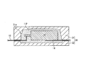
- FIG. 2 is a perspective view schematically showing the outer appearance of the exterior body according to the embodiment.
- FIG. 3 is a cross-sectional view of the exterior body of FIG. 2 taken along the line AA.
- FIG. 4 is an enlarged cross-sectional view showing a main part of the exterior body taken along the line AA of FIG.
- the electrolytic capacitor according to the present embodiment includes a capacitor element 10 having an anode part and a cathode part, an anode lead terminal (not shown) electrically connected to the anode part, and a cathode electrically connected to the cathode part.
- a lead terminal (not shown) and an outer package 11 that covers the capacitor element 10 are provided.
- the anode part has an anode body and an anode wire 2 extending from a planting surface 1X of the anode body.
- the exterior body 11 has a flat surface portion 11X, and has a first surface facing the planting surface 1X, and a second surface and a third surface sharing one side with the first surface and facing each other.
- the second surface and the third surface have plane portions 11Y and 11Z, respectively.
- the area of the flat surface portion 11Y of the second surface is approximately 108% of the area of the flat surface portion 11Z of the third surface, and the angle ⁇ 1 formed by the flat surface portion 11X of the first surface and the flat surface portion 11Y of the second surface is approximately 87. It is degree.
- the anode wire 2 includes a first portion (not shown) embedded in the anode body from the planting surface 1X and a first portion extending from the planting surface 1X to the flat surface portion 11X of the first surface of the exterior body 11. And two portions 2b.
- the first surface is formed with a first protruding portion 111 which is on the extension of the second portion 2b of the anode wire and which protrudes to the outside of the outer package 11.
- the first projecting portion 111 is formed in a virtual space formed by the flat surface portion 11X, the virtual first flat surface 11Xv, and the virtual third flat surface 11Zv.
- the angle ⁇ 2 formed by the imaginary first plane 11Xv and the second plane portion 11Y is about 89 degrees
- the angle ⁇ 3 formed by the imaginary first plane 11Xv and the imaginary third plane 11Zv is about 91 degrees. ..
- the first protruding portion 111 includes a protruding surface 111x and a plurality of rising surfaces (111y and 111z) connecting the protruding surface 111x and the flat surface portion 11X.
- the protruding surface 111x is in the vicinity of the first side 11a on the second surface (flat surface portion 11Y) side of the flat surface portion 11X of the first surface, and on the second surface side more than the position facing the second portion 2b of the anode wire. From the first surface (flat surface portion 11X) to a position that covers the portion of the anode wire that intersects with the extension line of the second portion 2b of the anode wire, the virtual third surface 11Zv.
- the first projecting portion 111 further includes a rising surface facing the rising surface 111y.
- the angle ⁇ 4 formed by the protruding surface 111x and the second surface flat portion 11Y is about 89 degrees, which is larger than the angle ⁇ 1 and is the same as the angle ⁇ 2. That is, the protruding surface 111x is on the same plane as the virtual first plane 11Xv.
- the length T1 of the first protrusion 111 in the thickness direction of the exterior body 11 is about 71% of the length T in the thickness direction between the second surface 11Y and the third surface 11Z.
- the ratio (W1/W) of the average length W1 in the width direction of the first protrusion 111 to the length W in the width direction of the flat surface portion 11X of the first surface is about 32%.
- the ratio (S1/S) of the area S1 of the first protruding portion 111 to the area S of the entire first surface is about 23%.
- the length L11 in the longitudinal direction A on the extension of the second portion 2b of the exterior body 11 has the maximum value within the range where the mold releasability of the mold is not impaired. Therefore, the length L1 required between the second portion 2b and the first surface of the outer package 11 and the length L2 of the second portion 2b required for joining the second portion 2b and the anode lead terminal It is possible to increase the length of the capacitor element 10 in the longitudinal direction A to the maximum value while ensuring the above.
- the mold used when forming the exterior body 11 The mold releasability of is not easily impaired.
- the exterior body 11 shown in FIGS. 2 to 4 includes a protrusion (second protrusion 112) other than the first protrusion in addition to the first protrusion 111.
- the second protrusion 112 in the illustrated example is formed in a strip shape along the first side 11a. Such a second protrusion 112 contributes to an improvement in mold releasability.
- the anode lead terminal joined to the anode wire may be led out from the first surface of the outer package.
- the led-out anode lead terminal is bent and covers, for example, a part of the third surface of the outer package.
- the electrolytic capacitor is mounted on the electronic device with the third surface of the outer casing facing the electronic device on which the electrolytic capacitor is mounted.
- the exposed portion of the anode lead terminal which is led out from the outer package, may be bent along the virtual first plane. Further, the exposed portion may be bent so as not to overlap the first protrusion. In this case, it is easy to suppress the outer dimension of the electrolytic capacitor from becoming larger than that of the outer package. As a result, the outer package can be made larger, and the size of the capacitor element can be made larger.
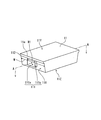
- FIG. 5 is a perspective view schematically showing an example of the electrolytic capacitor according to the present embodiment.
- FIG. 6 is a cross-sectional view taken along the line BB of the electrolytic capacitor of FIG.
- the electrolytic capacitor shown in FIGS. 5 and 6 includes the exterior body shown in FIGS. 2 to 4.
- the anode lead terminal 13 is led out of the exterior body 11 from the flat portion 11X of the first surface.
- the anode lead terminal 13 led out from the flat surface portion 11X is bent so that the surface (outer surface) 13X facing the outside thereof is along the virtual first flat surface 11Xv (see FIG. 4), and then the third surface of the outer package 11. Is bent along the flat surface portion 11Z.
- the portion (exposed portion) of the anode lead terminal 13 that is led out from the outer casing 11 does not overlap with the first protruding portion 111.
- the protruding surface and the outer surface 13X of the anode lead terminal are both on the same plane as the virtual first plane. Therefore, the outer dimensions of the electrolytic capacitor 20 are less likely to be larger than the outer casing 11. In other words, even when the outer casing 11 is formed with the first projecting portion 111 and the anode lead terminal 13 is arranged around the outer casing 11, the outer dimension of the electrolytic capacitor 20 becomes large. Can be suppressed. Therefore, the size of the capacitor element 10 can be increased.
- the cathode lead terminal 14 is also led out of the exterior body 11 from the surface of the exterior body 11 facing the flat surface portion 11X of the first surface, then bent, and placed on the third surface.
- the cathode lead terminal 14 is joined to the cathode portion of the capacitor element 10 by, for example, a conductive adhesive material (not shown).
- the first protruding portion 111 is arranged substantially in the center in the width direction of the flat surface portion 11X of the first surface of the outer package 11 so as to correspond to the second portion 2b of the anode wire 2.
- the anode lead terminal 13 is led out from two locations on the first surface 11X so as to avoid the first protruding portion 111. After that, the two strip-shaped anode lead terminals 13 are connected in a region on the virtual first surface 11Xv on the side of the third surface 11Z.
- an opening may be formed in the exposed portion of the anode lead terminal 13 so as to surround the periphery of the rising surface of the first protruding portion 111.
- expansion of the outer dimensions of the electrolytic capacitor 20 is suppressed.
- the length of the anode lead terminal 13 arranged on the third surface in the width direction is larger than the point derived from the outer package 11, the electric resistance is reduced, and the anode lead terminal 13 and the anode lead terminal 13 are illustrated. Not Widens the bonding area with electronic devices. Therefore, the connection reliability is improved.
- FIG. 7 is a perspective view schematically showing an electrolytic capacitor according to another embodiment.
- FIG. 8 is a cross-sectional view of the electrolytic capacitor taken along line CC of FIG.
- the first projecting portion 111 includes a projecting surface 111x and a plurality of rising surfaces (111y and 111z) that connect the projecting surface 111x and the first surface flat portion 11X.
- the protruding surface 111x is a part of the first side 11a, and extends from the vicinity of the center of the first side 11a. It extends toward the imaginary third plane 11Zv up to a position that covers a portion that intersects with the extension line of the two portions 2b.
- the exterior body 11 does not include the second protrusion.
- the exterior body shown in FIGS. 7 and 8 has the same configuration as the exterior body shown in FIGS. 2 to 4.
- the anode lead terminal 13 is led out of the exterior body 11 from the second surface.
- the anode lead terminal 13 led out from the second surface is arranged on the second surface as it is. Also in this case, since the anode lead terminal 13 does not overlap the first projecting portion 111, the outer dimensions of the electrolytic capacitor 20 are less likely to be larger than the outer casing 11. Therefore, the size of the capacitor element 10 can be increased.
- the cathode lead terminal 14 may be led out of the exterior body 11 from the second surface and placed on the second surface as it is.
- the cathode lead terminal 14 is joined to the cathode portion of the capacitor element 10 with, for example, a conductive adhesive material 8.
- the conductive adhesive 8 is, for example, a mixture of a thermosetting resin described later and carbon particles or metal particles.
- FIG. 9A is a perspective view schematically showing the electrolytic capacitor 100 according to the embodiment of the present invention.
- 9B is a sectional view taken along line X 1 -X 2 of electrolytic capacitor 100 in FIG. 9A.
- FIG. 10A and FIG. 10B are diagrams showing the manner of connecting the anode lead terminal 50 and the cathode lead terminal 60 to the capacitor element 10 with the outer package 70 omitted in FIGS. 9A and 9B, respectively.
- 10B is a sectional view taken along line Y 1 -Y 2 of the electrolytic capacitor in FIG. 10A.
- the electrolytic capacitor 100 includes a capacitor element 10 having an anode part 6 and a cathode part 7, an anode lead terminal (anode lead frame) 50 electrically connected to the anode part 6, and a cathode lead electrically connected to the cathode part 7.
- a terminal (cathode lead frame) 60 and an outer package 70 are provided.
- the outer package 70 covers the capacitor element 10 with a part of the anode lead terminal 50 and the cathode lead terminal 60 exposed.
- the anode part 6 has an anode body 1 and an anode wire 2 extending from the anode body 1, and the anode wire 2 is bonded to an anode lead terminal 50.
- the outer surface of the outer package 70 is a first surface A1, a second surface A2 that shares one side with the first surface A1, and a surface that shares one side with the first surface A1 and is opposite to the second surface A2.
- the fourth surface A4 is located on the opposite side of the first surface A1 (see FIG. 9B).
- the anode lead terminal 50 has a first anode lead portion 51, a second anode lead portion 52, and a third anode lead portion 53.
- the third anode lead portion 53 further includes a first region 53a extending in a direction along the first surface A1 (more specifically, a direction along a virtual first plane), and a third region bent from the first region 53a. And a second region 53b extending along the surface A3 (see FIGS. 10A and 10B).
- the anode lead terminal 50 is bent from the first main surface A1 at the first bent portion B1 and the second bent portion B2.
- a part of the anode lead frame 50 is bent in the direction toward the anode wire 2 at the first bent portion B1 to form a second anode lead portion 52.
- Another part of the anode lead terminal 50 is bent along the first surface A1 at the second bent portion B2 to form the third anode lead portion 53.
- the remaining part of the anode lead frame 50 along the second surface A2 constitutes the first anode lead part 51.
- the second anode lead portion 52 is connected to the anode wire 2.
- the entire third anode lead portion 53 is exposed from the outer package 70, and the third anode lead portion 53 covers the first surface A1 in the first region 53a.
- the third anode lead portion 53 covers the first surface A1 in the first region 53a.
- the first bent portion B1 is located closer to the capacitor element 10 side than the second bent portion B2. That is, the second anode lead portion 52 is bent at a position closer to the cathode portion of the capacitor element than the third anode lead portion 53. Due to this, as shown in FIG. 10A, the anode lead terminal 50 has an opening formed on the first surface side.
- the first region 53a exposed from the outer package 70 does not cover the entire first surface, and the region where the anode lead terminal 50 (third anode lead portion 53) is not exposed corresponds to the opening. It exists in the area (third area) on the first surface.
- a protrusion (first protrusion) 71 is provided in a region on the first surface corresponding to the opening, and a first region 53 a extends so as to surround the protrusion 71. There is.
- the anode wire 2 extends toward the protrusion 71 (see FIG. 10A, but the protrusion 71 is not shown in FIG. 10A).
- the cathode lead terminal has a first cathode lead portion 61 and a second cathode lead portion 62.
- a part of the cathode lead terminal 60 is bent along the second surface A2 to the fourth surface A4, the bent portion constitutes the first cathode lead portion 61, and the remaining portion constitutes the second cathode lead portion 62.
- the first cathode lead portion 61 is electrically connected to the cathode portion of the capacitor element 10 on the second surface A2 side via a conductive adhesive (not shown) (for example, silver paste).
- the second cathode lead portion 62 further has a first area 62a extending in the direction along the fourth surface A4 and a second area 62b bent from the first area 62a and extending along the third surface A3. As shown in FIG. 10B, the entire second cathode lead portion 62 including the first region 62a and the second region 62b is exposed from the outer package 70.
- the cathode lead terminal 60 similarly to the anode lead terminal 50, the cathode lead terminal 60 also has an opening formed on the fourth surface A4 side.
- the first region 62a of the cathode lead terminal 60 exposed from the outer package 70 does not cover the entire fourth surface A4, and the region where the cathode lead terminal 60 (second cathode lead portion 62) is not exposed is It exists in the area
- a projecting portion 72 is provided in a region on the fourth surface corresponding to the opening, and a first region 62a is formed so as to surround the projecting portion 72.
- the distance from the second surface A2 where the cathode lead terminal 60 and the cathode part are electrically connected to the capacitor element 10 is usually the outer package. Is smaller than the distance from the third surface A3 to the capacitor element 10 (that is, the thickness of the exterior body covering the third main surface A3 side of the cathode portion). Therefore, from the viewpoint of ensuring insulation between the cathode portion and the anode lead terminal 50, the end portion position L 1 of the first anode lead portion 51 shown in FIG. 10B and the end portion on the first surface side of the cathode portion of the capacitor element. It becomes necessary to provide a certain distance from the position L 2 .
- the area of the first anode lead portion 51 is reduced by providing the second anode lead portion 52.
- the area of the first anode lead portion 51 is limited by the arrangement of the second anode lead portion and the cathode portion, and it has been necessary to devise to expand the land area for connection with the external substrate.
- the first cathode lead part 61 is bent inside the outer package 70 to increase the thickness of the outer package covering the first surface A1 side of the cathode part.
- the thickness of the outer casing is increased, the volume occupied by the capacitor element is reduced and the capacitance is reduced.
- the electrolytic capacitor 100 is electrically connected to the external substrate by the third surface on the side opposite to the second surface A1 on which the cathode lead terminal 60 and the cathode portion are electrically connected. Done on surface A3. Therefore, the shape and area of the third anode lead portion 53 can be set arbitrarily regardless of the arrangement of the cathode portion. As shown in FIG. 10B, the end position L 3 of the third anode lead portion 53 can be set to a position exceeding L 2 and overlapping with the cathode portion. As a result, the area of the third anode lead portion 53 can be increased and the reliability of connection with the external substrate can be improved without reducing the capacitance.
- FIG. 11 is a sectional view schematically showing an example of the capacitor element according to the present embodiment.
- the capacitor element 10 includes an anode part 6 and a cathode part 7.
- the anode part 6 has an anode body 1 having a dielectric layer 3 and an anode wire 2.
- the cathode part 7 has a solid electrolyte layer 4 formed on the dielectric layer 3, and a cathode layer 5 (carbon layer 5a and metal paste layer 5b) that covers the surface of the solid electrolyte layer 4.
- the anode wire 2 has a first portion 2a embedded from one surface (planting surface) of the anode body 1 into the inside of the anode body 1, and a second portion 2b extending from the one surface of the anode body 1.
- the anode part has, for example, an anode body and an anode wire extending from one surface of the anode body and electrically connected to the anode lead terminal.
- the anode body is, for example, a rectangular parallelepiped porous sintered body obtained by sintering metal particles.
- the metal particles particles of valve action metal such as titanium (Ti), tantalum (Ta), niobium (Nb) are used.
- One type or two or more types of metal particles are used for the anode body.
- the metal particles may be an alloy composed of two or more kinds of metals. For example, an alloy containing a valve metal and silicon, vanadium, boron or the like can be used. Alternatively, a compound containing a valve metal and a typical element such as nitrogen may be used.
- the alloy of the valve action metal contains the valve action metal as a main component and contains, for example, 50 atom% or more of the valve action metal.
- the anode wire is made of a conductive material.
- the material for the anode wire is not particularly limited, and examples thereof include copper, aluminum, and aluminum alloys in addition to the above valve action metal.
- the materials forming the anode body and the anode wire may be the same or different.
- the cross-sectional shape of the anode wire is not particularly limited, and examples thereof include a circle, a track shape (a shape including straight lines parallel to each other and two curves connecting the ends of these straight lines), an ellipse, a rectangle, and a polygon. .
- the anode part is produced, for example, by pressure-molding a rectangular parallelepiped in a state where the first part is embedded in the powder of the metal particles and sintering.
- the second portion of the anode wire is pulled out from one surface of the anode body so as to stand.
- the second portion is joined to the anode lead terminal by welding or the like, and the anode wire and the anode lead terminal are electrically connected.
- the welding method is not particularly limited, and examples thereof include resistance welding and laser welding.
- a dielectric layer is formed on the surface of the anode body.
- the dielectric layer is made of, for example, a metal oxide.
- a method of forming a layer containing a metal oxide on the surface of the anode body for example, a method of anodizing the surface of the anode body by dipping the anode body in a chemical conversion solution, or the anode body under an atmosphere containing oxygen. The method of heating is mentioned.
- the dielectric layer is not limited to the layer containing the above metal oxide, and may have an insulating property.
- the cathode part has a solid electrolyte layer formed on the dielectric layer and a cathode layer covering the solid electrolyte layer.
- the solid electrolyte layer may be formed so as to cover at least a part of the dielectric layer.
- a manganese compound or a conductive polymer is used for the solid electrolyte layer.
- the conductive polymer include polypyrrole, polythiophene, polyfuran, polyaniline, polyacetylene, polyphenylene, polyparaphenylenevinylene, polyacene, polythiophenvinylene, polyfluorene, polyvinylcarbazole, polyvinylphenol, polypyridine, and derivatives of these polymers.
- the conductive polymer may be a copolymer of two or more kinds of monomers. It may be polythiophene, polyaniline, or polypyrrole in terms of excellent conductivity. In particular, polypyrrole may be used because it is excellent in water repellency.
- the solid electrolyte layer containing the conductive polymer is formed, for example, by polymerizing raw material monomers on the dielectric layer. Alternatively, it is formed by applying a liquid containing the conductive polymer to the dielectric layer.
- the solid electrolyte layer is composed of one or more solid electrolyte layers. When the solid electrolyte layer is composed of two or more layers, the composition and forming method (polymerization method) of the conductive polymer used in each layer may be different.
- polypyrrole, polythiophene, polyfuran, polyaniline and the like mean polymers having a basic skeleton of polypyrrole, polythiophene, polyfuran, polyaniline and the like, respectively. Therefore, polypyrrole, polythiophene, polyfuran, polyaniline and the like may include their respective derivatives.
- polythiophene includes poly(3,4-ethylenedioxythiophene) and the like.
- various dopants may be added to the polymerization liquid for forming the conductive polymer, the solution or the dispersion liquid of the conductive polymer.
- the dopant is not particularly limited, 1,5-naphthalenedisulfonic acid, 1,6-naphthalenedisulfonic acid, 1-octanesulfonic acid, 1-naphthalenesulfonic acid, 2-naphthalenesulfonic acid, 2,6-naphthalenedisulfonic acid, 2,7-naphthalenedisulfonic acid, 2-methyl-5-isopropylbenzenesulfonic acid, 4-octylbenzenesulfonic acid, 4-nitrotoluene-2-sulfonic acid, m-nitrobenzenesulfonic acid, n-octylsulfonic acid, n-butane Sulfonic acid, n-hexanesulfonic acid, o-nitrobenzenesul
- the derivative examples include metal salts such as lithium salt, potassium salt and sodium salt, ammonium salts such as methylammonium salt, dimethylammonium salt and trimethylammonium salt, piperidinium salt, pyrrolidinium salt and pyrrolinium salt.
- metal salts such as lithium salt, potassium salt and sodium salt
- ammonium salts such as methylammonium salt, dimethylammonium salt and trimethylammonium salt
- piperidinium salt such as pyrrolidinium salt and pyrrolinium salt.
- the average particle diameter D50 of the particles is, for example, 0.01 ⁇ m or more and 0.5 ⁇ m or less. When the average particle diameter D50 of the particles is within this range, the particles easily penetrate into the inside of the anode body.
- the cathode layer has, for example, a carbon layer formed so as to cover the solid electrolyte layer, and a metal paste layer formed on the surface of the carbon layer.
- the carbon layer contains a conductive carbon material such as graphite and a resin.
- the metal paste layer contains, for example, metal particles (for example, silver) and a resin.
- the configuration of the cathode layer is not limited to this configuration.
- the cathode layer may have any structure as long as it has a current collecting function.
- ⁇ Anode lead terminal> One end of the anode lead terminal is joined to the anode wire by a conductive adhesive material, solder, resistance welding or laser welding. The other end of the anode lead terminal is led out from the exterior body. A part of the exposed portion of the anode lead terminal is arranged on either surface of the outer package together with the cathode lead terminal.
- the material of the anode lead terminal is not particularly limited as long as it is electrochemically and chemically stable and has conductivity.
- the anode lead terminal may be a metal such as copper or a nonmetal.
- the shape is not particularly limited as long as it is flat.
- the thickness of the anode lead terminal (the length between the main surfaces of the anode lead terminal) may be 25 ⁇ m or more and 200 ⁇ m or less, or 25 ⁇ m or more and 100 ⁇ m or less from the viewpoint of reducing the height.
- the anode lead terminal may be joined to the anode wire by a conductive adhesive or solder, or may be joined to the anode wire by resistance welding or laser welding.
- the conductive adhesive is, for example, a mixture of a thermosetting resin described below and carbon particles or metal particles.
- the cathode lead terminal is bonded to the cathode layer via, for example, a conductive adhesive material.
- One end of the cathode lead terminal is arranged inside the outer package.
- the other end of the cathode lead terminal is led out from the exterior body.
- a part of the exposed portion of the cathode lead terminal is arranged on either surface of the outer package together with the anode lead terminal.
- the material of the cathode lead terminal is not particularly limited as long as it is electrochemically and chemically stable and has conductivity.
- the cathode lead terminal may be a metal such as copper or a nonmetal.
- the shape is also not particularly limited, and is, for example, long and flat.
- the thickness of the cathode lead terminal may be 25 ⁇ m or more and 200 ⁇ m or less, or 25 ⁇ m or more and 100 ⁇ m or less, from the viewpoint of reducing the height.
- the outer package is provided to electrically insulate the anode lead terminal and the cathode lead terminal, and is made of an insulating material (exterior body material).
- the exterior body material includes, for example, a thermosetting resin.
- the thermosetting resin include epoxy resin, phenol resin, silicone resin, melamine resin, urea resin, alkyd resin, polyurethane, polyimide and unsaturated polyester.
- the electrolytic capacitor includes, for example, a preparation step (S1) of preparing a capacitor element to which an anode lead terminal and a cathode lead terminal are connected, a capacitor element, a part of the anode lead terminal, and a part of the cathode lead terminal. It is manufactured by a method including a sealing step (S2) of forming an outer package to be sealed and a bending step (S3) of bending an exposed portion of the anode lead terminal exposed from the outer package.
- FIG. 12 is a flowchart showing the method of manufacturing the electrolytic capacitor according to the present embodiment.
- the manufacturing method of the electrolytic capacitor according to the present embodiment will be described in detail, taking the case of manufacturing the electrolytic capacitor shown in FIGS. 5 and 6 as an example.
- the exterior body has a second surface and a third surface that share one side with the first surface and that face each other, and the area of the second surface is larger than the area of the third surface.
- the first surface, the second surface, and the third surface each have a flat surface portion, and an angle ⁇ 1 formed by the flat surface portion of the first surface and the flat surface portion of the second surface is less than 90 degrees.
- the first projecting portion shares the first surface on the second surface side of the first surface with the first surface, and the angle ⁇ 2 formed by the second surface flat portion is larger than the angle ⁇ 1 and 90 degrees or less. Is formed in a virtual space R formed by a virtual first plane and a virtual third plane that is on the same plane as the plane portion of the third surface.
- the first protruding portion includes a protruding surface and a plurality of rising surfaces that connect the protruding surface and the first surface, and the protruding surface is on the same plane as the virtual first surface.
- the manufacturing method according to the present embodiment is useful when the outer shape of the exterior body is tapered and the exterior body has the first protruding portion.
- a capacitor element is prepared.
- the valve action metal particles and the anode wire are put into a mold so that the first part is embedded in the valve action metal particles, pressure-molded, and then sintered in a vacuum, whereby the first part is made of a porous sintered body.
- An anode part to be embedded inside is prepared from one surface.
- the pressure at the time of pressure molding is not particularly limited and is, for example, about 10 N or more and 100 N or less.
- the valve action metal particles may be mixed with a binder such as polyacrylic carbonate, if necessary.
- a dielectric layer is formed on the anode body.
- the anode body is immersed in a chemical conversion tank filled with an electrolytic aqueous solution (for example, phosphoric acid aqueous solution), and the second portion of the anode wire is connected to the anode body of the chemical conversion tank to perform anodization.
- an electrolytic aqueous solution for example, phosphoric acid aqueous solution
- the dielectric layer made of the oxide film of the valve metal can be formed on the surface of the anode body.
- the electrolytic aqueous solution is not limited to the phosphoric acid aqueous solution, and nitric acid, acetic acid, sulfuric acid or the like can be used.
- the solid electrolyte layer containing a conductive polymer is, for example, a method of impregnating an anode body on which a dielectric layer is formed with a monomer or oligomer, and then polymerizing the monomer or oligomer by chemical polymerization or electrolytic polymerization, or The anode body on which the body layer is formed is impregnated with a solution or dispersion of a conductive polymer and dried to form at least a part of the dielectric layer.
- a carbon paste and a metal paste are sequentially applied to the surface of the solid electrolyte layer to form a cathode layer composed of the carbon layer and the metal paste layer.
- the structure of the cathode layer is not limited to this, and may be any structure having a current collecting function.
- the capacitor element is manufactured by the above method.
- the anode lead terminal and the cathode lead terminal are prepared and joined to the capacitor element.
- a bent portion (internal bent portion) arranged inside the outer package is formed on the anode lead terminal.
- the internal bent portion is formed by, for example, press working.
- the position of the internal bent portion of the anode lead terminal is appropriately set according to the length and diameter of the anode wire.
- An internal bent portion may be formed also in the cathode lead terminal.
- the capacitor element Place the capacitor element with each lead terminal placed.
- the second portion of the anode wire and the vicinity of one end of the anode lead terminal are joined by laser welding or resistance welding.
- the vicinity of one end of the cathode lead terminal is joined to the cathode layer via a conductive adhesive.
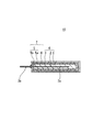
- FIG. 13A is a cross-sectional view schematically showing the capacitor element to which the lead terminals prepared in the preparation step of the manufacturing method according to the present embodiment are joined.
- the capacitor element 10 includes the anode wire 2 that is planted from the planting surface 1X.
- An anode lead terminal 13 is joined to the anode wire 2 (second portion 2b).
- a cathode lead terminal 14 is joined to the cathode portion of the capacitor element 10.
- a bent portion corresponding to the inner bent portion is formed in the anode lead terminal 13.
- the materials of the capacitor element and the outer casing are placed in a mold, and the capacitor element is sealed by a transfer molding method, a compression molding method, or the like. At this time, a part of the anode lead terminal and the cathode lead terminal is led out from the mold.
- the molding conditions are not particularly limited, and the time and temperature conditions may be appropriately set in consideration of the curing temperature of the thermosetting resin used.
- FIG. 13B is a sectional view schematically showing the mold and the capacitor element housed in the mold in the sealing step of the manufacturing method according to the present embodiment.
- the capacitor element 10 is housed in the mold 30 together with the outer package material 11P. A part of the anode lead terminal 13 and the cathode lead terminal 14 is led out from the mold 30.
- the mold 30 includes a deep first mold 31 that can accommodate the capacitor element 10 and a second mold 32 that has a shallow step.
- the first mold 31 is formed with a recess 31a for forming the first protrusion.
- the bottom surface of the first mold 31 is narrower than the area of the opening, and the first mold 31 has a tapered shape.
- the first mold 31 and the second mold 32 are fitted to each other to form the container-shaped mold 30.
- the anode lead terminal 13 and the cathode lead terminal 14 are led out to the outside through a gap generated when the first die 31 and the second die 32 are fitted together.
- an electrolytic capacitor including a capacitor element, an anode lead terminal, a cathode lead terminal, and an exterior body that covers a part of the capacitor element and each lead terminal can be obtained.
- FIG. 13C is a sectional view schematically showing how the first mold is released in the sealing step of the manufacturing method according to the present embodiment.
- the capacitor element 10 is taken out, for example, the second mold 32 is fixed and the first mold 31 is moved in a direction in which it is separated from the capacitor element 10.
- the anode lead terminal is bent along the virtual first plane (see FIG. 4).
- the first projecting portion formed on the side surface of the exterior body may be used as a guide.
- the anode lead terminal is bent by moving the bending roller from the second surface toward the third surface of the exterior body while pressing the bending roller against the first protrusion. In this case, since the bending roller is stably moved, the bending accuracy is improved.
- FIG. 13D is a sectional view schematically showing how the anode lead terminal is bent in the bending step of the manufacturing method according to the present embodiment.
- the bending roller 40 moves from the second surface (flat surface portion 11Y) of the exterior body 11 toward the third surface (flat surface portion 11Z) while being guided by the first protruding portion 111.
- the anode lead terminal 13 is pressed by the bending roller 40 and bent in a shape along the imaginary first plane.
- the protruding surface of the first protruding portion 111 and the outer surface 13X of the anode lead terminal 13 are both on the same plane as the virtual first plane 11Xv.
- the anode lead terminal 13 is then further bent along the third surface.
- the cathode lead terminal 14 may be bent by using a bending roller.
- the anode lead terminal (anode lead frame) 50 shown in FIG. 14 may be used in the preparation process. As a result, the electrolytic capacitor 100 shown in FIG. 9A can be manufactured.
- a U-shaped cut C is formed along the contour line of the formation region (for example, a rectangular region) of the second anode lead portion 52, except for one straight side of the contour line. (Dashed line part) is formed.
- the punching of the anode lead terminal 50 and the formation of the cut may be performed at the same time.
- the portion in which the cut is not formed is the first bent portion B1. It should be noted that in FIG. 14, the alternate long and short dash line is the portion that serves as the axis of the bending process.
- the cut length U may be longer than the height of the anode wire 2 from the second surface A2.
- the anode lead terminal (third anode lead portion) is arranged around the first projecting portion of the outer package, and the anode lead terminal does not cover the first projecting portion. 50 may form a through hole 54 adjacent to the notch.
- the formation region of the second anode lead portion 52 is bent around the first bent portion B1 as an axis, and the second anode lead portion 52 is erected from the anode lead frame.
- the bent portion is formed by bending, for example.
- the position of the first bent portion B1 may be appropriately set according to the size of the capacitor element and the like (in particular, the position of the extending portion of the anode wire 2 in the capacitor element).
- the anode lead terminal 50 is bent from the direction along the second surface A2 to the direction along the first surface A1, and further from the direction along the first surface A1 to the third surface A3 facing the second surface A2. It is bent along the direction.
- the cathode lead terminal is bent from the direction along the second surface A2 to the direction along the fourth surface A4, and further from the direction along the fourth surface A4 along the third surface A3 facing the second surface A2. To be bent.
- the boundary between the portion along the first main surface A1 and the portion along the second main surface A2 is the second bent portion B2.
- a part of the anode lead terminal 50 extending in a direction away from the outer package 70 forms a third anode lead portion 53 with the second bent portion B2 as a reference.
- the portion excluding the second anode lead portion 52 constitutes the first anode lead portion 51.
- the cathode lead terminal 60 a part of the cathode lead terminal 60 extending in a direction away from the outer package 70 with reference to a boundary between a portion along the first main surface A1 and a portion along the fourth main surface A4. Constitutes the second cathode lead portion 62, and the remaining portion constitutes the first cathode lead portion 61.
- the electrolytic capacitor according to the present invention can be used in various applications because the size of the capacitor element can be increased. While the present invention has been described in terms of its presently preferred embodiments, such disclosure should not be construed as limiting. Various variations and modifications will no doubt become apparent to those skilled in the art to which the present invention pertains upon reading the above disclosure. Therefore, the appended claims should be construed to cover all variations and modifications without departing from the true spirit and scope of the present invention.
- Electrolytic capacitor 10 Capacitor element 1: Anode body 1X: Embedding surface 2: Anode wire 2a: First part 2b: Second part 3: Dielectric layer 4: Solid electrolyte layer 5: Cathode layer 5a: Carbon layer 5b: Metal paste layer 6: Anode part 7: Cathode part 8: Conductive adhesive material 11, 70: Outer package A1: First surface A2: Second surface A3: Third surface A4: Fourth surface 11X: First surface (Flat part) 11Y: Second surface (flat surface portion) 11Z: Third surface (flat surface portion) 11Xv: Virtual 1st plane 11Zv: Virtual 3rd plane 11a: 1st side 111: 1st protrusion part 111x: Protrusion surface 111y, 111z: Rising surface 112: 2nd protrusion part 11P: Material 71, 72 of an exterior body.
Abstract
Provided is an electrolytic capacitor comprising: a capacitor element that has a positive electrode part and a negative electrode part; a positive electrode lead terminal that is electrically connected to the positive electrode part; a negative electrode lead terminal that is electrically connected to the negative electrode part; and an exterior body that covers the capacitor element, wherein the positive electrode part has a positive electrode body and a positive electrode wire extending from an implantation surface of the positive electrode body to the outside of the positive electrode body, the exterior body has a first surface facing the implantation surface, and a second surface and a third surface sharing one side with the first surface and facing each other, the area of the second surface is larger than the area of the third surface, an angle θ1 between the first surface and the second surface is less than 90 degrees, and the first surface includes a protrusion part that is on an extension of the positive electrode wire and protrudes outward of the exterior body.
Description
本発明は、電解コンデンサおよびその製造方法に関する。
The present invention relates to an electrolytic capacitor and a method for manufacturing the same.
電解コンデンサは、等価直列抵抗(ESR)が小さく、周波数特性が優れているため、様々な電子機器に搭載されている。電解コンデンサは、陽極部および陰極部を備えるコンデンサ素子と、陽極部と電気的に接続する陽極リード端子と、陰極部と電気的に接続する陰極リード端子とを備える。コンデンサ素子は、通常、外装体により封止されている。
Electrolytic capacitors have a small equivalent series resistance (ESR) and excellent frequency characteristics, so they are used in various electronic devices. The electrolytic capacitor includes a capacitor element having an anode part and a cathode part, an anode lead terminal electrically connected to the anode part, and a cathode lead terminal electrically connected to the cathode part. The capacitor element is usually sealed with an exterior body.
コンデンサ素子の封止は、例えば、コンデンサ素子および外装体の材料(未硬化の熱硬化性樹脂およびフィラー)を金型に収容し、トランスファー成型法、圧縮成型法等により行われる。このとき、金型の離型性を考慮して、外装体の側面はテーパ状に設計される(特許文献1参照)。
The encapsulation of the capacitor element is performed by, for example, a transfer molding method, a compression molding method, etc., in which the materials of the capacitor element and the outer casing (uncured thermosetting resin and filler) are housed in a mold. At this time, the side surface of the exterior body is designed in a tapered shape in consideration of the mold releasability (see Patent Document 1).
電子機器の多機能化および小型化に伴い、電解コンデンサには、高容量かつ小型であることが求められる。しかし、例えば、直方体の外装体の側面をテーパ状にすると、直方体の外装体と比較してその体積が小さくなるため、封止できるコンデンサ素子も小さくなる。
With the increasing functionality and miniaturization of electronic devices, electrolytic capacitors are required to have high capacity and small size. However, for example, when the side surface of the rectangular parallelepiped exterior body is tapered, its volume is smaller than that of the rectangular parallelepiped exterior body, so that the capacitor element that can be sealed is also small.
本発明の第一の局面は、陽極部および陰極部を備えるコンデンサ素子と、前記陽極部と電気的に接続される陽極リード端子と、前記陰極部と電気的に接続される陰極リード端子と、前記コンデンサ素子を覆う外装体と、を備え、前記陽極部は、陽極体と、前記陽極体の植立面から前記陽極体の外部方向へ延出する陽極ワイヤと、を有し、前記外装体は、前記植立面に対向する第1面と、前記第1面と一辺を共有し、かつ、互いに対向する第2面および第3面と、を有し、前記第1面、前記第2面および前記第3面はそれぞれ平面部を有し、前記第2面の面積は、前記第3面の面積より大きく、前記第1面の平面部と前記第2面の平面部との成す角度θ1は90度未満であり、前記第1面は、前記陽極ワイヤの延長上にあり、かつ、前記第1面の平面部から前記外装体の外側へと突出する突出部を備える、電解コンデンサに関する。
A first aspect of the present invention, a capacitor element having an anode portion and a cathode portion, an anode lead terminal electrically connected to the anode portion, a cathode lead terminal electrically connected to the cathode portion, An exterior body covering the capacitor element, wherein the anode part has an anode body and an anode wire extending from the erected surface of the anode body toward the outside of the anode body. Has a first surface facing the planting surface, and a second surface and a third surface sharing one side with the first surface and facing each other, the first surface, the second surface The surface and the third surface each have a flat surface portion, the area of the second surface is larger than the area of the third surface, and the angle formed by the flat surface portion of the first surface and the flat surface portion of the second surface. [theta]1 is less than 90[deg.], the first surface is on the extension of the anode wire, and the electrolytic capacitor is provided with a protruding portion protruding from the flat surface portion of the first surface to the outside of the outer package. ..
本発明の第二の局面は、陽極リード端子および陰極リード端子が接続されたコンデンサ素子を準備する準備工程と、前記コンデンサ素子と、前記陽極リード端子の一部と、前記陰極リード端子の一部と、を封止する外装体を形成する封止工程と、前記陽極リード端子の前記外装体から露出する露出部を屈曲させる屈曲工程と、を備え、前記封止工程で形成される外装体の第1面は、前記外装体の外側へと突出する突出部を備え、前記屈曲工程において、前記陽極リード端子の前記露出部は、前記突出部に沿って移動するローラによって屈曲される、電解コンデンサの製造方法に関する。
A second aspect of the present invention is a preparation step of preparing a capacitor element to which an anode lead terminal and a cathode lead terminal are connected, the capacitor element, a part of the anode lead terminal, and a part of the cathode lead terminal. And a bending step of bending an exposed portion of the anode lead terminal exposed from the outer package, and a sealing step of forming an outer package that seals The first surface includes a protrusion that protrudes to the outside of the exterior body, and in the bending step, the exposed portion of the anode lead terminal is bent by a roller that moves along the protrusion. Manufacturing method.
本発明によれば、コンデンサ素子のサイズを大きくすることができる。
本発明の新規な特徴を添付の請求の範囲に記述するが、本発明は、構成および内容の両方に関し、本発明の他の目的および特徴と併せ、図面を照合した以下の詳細な説明によりさらによく理解されるであろう。 According to the present invention, the size of the capacitor element can be increased.
While the novel features of the invention are set forth in the appended claims, the invention is further described by the following detailed description in conjunction with the drawings, together with other objects and features of the invention, both in terms of structure and content. It will be well understood.
電解コンデンサの外寸法は、通常、厳密に定められている。そのため、高容量化するには、電解コンデンサの外寸法を変えることなく、封止されるコンデンサ素子を大きくすることが必要である。
The outer dimensions of electrolytic capacitors are usually strictly defined. Therefore, in order to increase the capacity, it is necessary to increase the size of the sealed capacitor element without changing the outer dimensions of the electrolytic capacitor.
図15は、従来の外装体を模式的に示す断面図である。
コンデンサ素子210は、陽極体と電気的に接続し、かつ、陽極体の1つの面(植立面)から植立する陽極ワイヤ202を備える。陽極ワイヤ202を外装体211から露出させないために、陽極ワイヤ202と、陽極ワイヤ202の延長上にある外装体211の側面211Xとの間には、一定の長さL1が確保される。また、陽極ワイヤ202には、図示しない陽極リード端子が接合される。陽極リード端子の接合部分を確保するため、陽極ワイヤ202の植立している部分の長さL2も一定以上必要である。 FIG. 15: is sectional drawing which shows the conventional exterior body typically.
Thecapacitor element 210 includes an anode wire 202 that is electrically connected to the anode body and that is erected from one surface (planting surface) of the anode body. In order to prevent the anode wire 202 from being exposed from the exterior body 211, a certain length L1 is secured between the anode wire 202 and the side surface 211X of the exterior body 211 which is an extension of the anode wire 202. Further, an anode lead terminal (not shown) is joined to the anode wire 202. In order to secure the joint portion of the anode lead terminal, the length L2 of the portion where the anode wire 202 is erected needs to be a certain length or more.
コンデンサ素子210は、陽極体と電気的に接続し、かつ、陽極体の1つの面(植立面)から植立する陽極ワイヤ202を備える。陽極ワイヤ202を外装体211から露出させないために、陽極ワイヤ202と、陽極ワイヤ202の延長上にある外装体211の側面211Xとの間には、一定の長さL1が確保される。また、陽極ワイヤ202には、図示しない陽極リード端子が接合される。陽極リード端子の接合部分を確保するため、陽極ワイヤ202の植立している部分の長さL2も一定以上必要である。 FIG. 15: is sectional drawing which shows the conventional exterior body typically.
The
ところが、側面211Xがテーパ形状であると、陽極ワイヤ202が配置されている辺りの外装体211の、陽極ワイヤ202の長手方向Aにおける長さL211は、電解コンデンサの長手方向Aにおける設計値Lより少なくとも長さL3の分、短くなる。つまり、コンデンサ素子210のサイズは、上記長さL1および長さL2に加えて、短くなったL3も考慮して決定しなければならない。そのため、設計値Lに対して、コンデンサ素子210の長手方向Aにおける長さはさらに小さくなる。
However, if the side surface 211X has a tapered shape, the length L211 of the exterior body 211 around the anode wire 202 in the longitudinal direction A of the anode wire 202 is smaller than the design value L in the longitudinal direction A of the electrolytic capacitor. It becomes shorter by at least the length L3. That is, the size of the capacitor element 210 must be determined in consideration of the shortened L3 in addition to the length L1 and the length L2. Therefore, the length in the longitudinal direction A of the capacitor element 210 becomes smaller than the design value L.
そこで、本実施形態では、外装体の陽極ワイヤの延長上にある一面(第1面)に突出部を設けて、テーパによって短くなったL3の少なくとも一部を補う。これにより、外装体の陽極ワイヤの長手方向Aにおける長さは、設計値Lに近づく。よって、上記長さL1および長さL2を確保しながら、コンデンサ素子の長手方向Aにおける長さを大きくすることができる。加えて、上記第1面には突出部が設けられるものの、第1面の他の部分はテーパ形状が維持されているため、金型の離型性も損なわれ難い。
Therefore, in the present embodiment, a protrusion is provided on one surface (first surface) on the extension of the anode wire of the outer package to supplement at least part of L3 shortened by the taper. As a result, the length of the anode wire in the longitudinal direction A of the outer package approaches the design value L. Therefore, the length in the longitudinal direction A of the capacitor element can be increased while securing the length L1 and the length L2. In addition, although the protruding portion is provided on the first surface, since the taper shape is maintained on the other portions of the first surface, the mold releasability of the mold is not easily impaired.
すなわち、本実施形態に係る電解コンデンサは、陽極部および陰極部を備えるコンデンサ素子と、陽極部と電気的に接続される陽極リード端子と、陰極部と電気的に接続される陰極リード端子と、コンデンサ素子を覆う外装体と、を備える。陽極部は、陽極体と、陽極体の植立面から陽極体の外部方向へ延出する陽極ワイヤと、を有する。外装体は、植立面に対向する第1面と、第1面と一辺を共有し、かつ、互いに対向する第2面および第3面と、を有する。第1面、第2面および第3面はそれぞれ平面部を有する。第2面の面積は、第3面の面積より大きい。第1面の平面部と第2面の平面部との成す角度θ1は90度未満である。第1面は、陽極ワイヤの延長上にあり、かつ、外装体の外側へと突出する突出部を備える。
That is, the electrolytic capacitor according to the present embodiment is a capacitor element including an anode part and a cathode part, an anode lead terminal electrically connected to the anode part, and a cathode lead terminal electrically connected to the cathode part, And an exterior body that covers the capacitor element. The anode part has an anode body and an anode wire extending from the planting surface of the anode body toward the outside of the anode body. The exterior body has a first surface that faces the planting surface, and a second surface and a third surface that share one side with the first surface and that face each other. The first surface, the second surface, and the third surface each have a flat surface portion. The area of the second surface is larger than the area of the third surface. The angle θ1 formed by the flat portion of the first surface and the flat portion of the second surface is less than 90 degrees. The first surface is provided on the extension of the anode wire and includes a protrusion that protrudes to the outside of the outer package.
第2面の面積は、第3面の面積より大きく、例えば、第3の面積の102%以上であり、105%以上である。また、第2面の面積は、第3面の面積の120%以下であってよく、115%以下であってよい。なお、この場合の面積は、表面積ではなく、第2面または第3面の法線方向から見た場合の投影面積(通常、電解コンデンサの上面または下面から見た場合の投影面積)を指す。
The area of the second surface is larger than the area of the third surface, for example, 102% or more of the third area, and 105% or more. The area of the second surface may be 120% or less of the area of the third surface, and may be 115% or less. The area in this case is not the surface area, but the projected area when viewed from the normal direction of the second surface or the third surface (usually the projected area when viewed from the upper surface or the lower surface of the electrolytic capacitor).
外装体の第1面~第3面は、通常、略直方体をなすように形成された外装体の外表面の6つの主面のうちの3つを意味する。外装体の外表面は、また、第2面および第3面のそれぞれと一辺を共有し且つ第1面と反対側に位置する第4面を有し得る。この場合、第1面~第4面は、通常、略直方体の互いに対向する2面を除く4つの主面を指す。これら第1面~第4面は平面部を有しており、平面部同士のなす角度により、外装体の2つの面同士がなす角度を定義できる。しかしながら、第1面~第4面は、平面部を有する限りにおいて、曲面形状の部分を有していたり、若干の凹凸を含んでいたり、および/または、複数の屈曲した平面により形成されていたりしてもよい。第1面~第4面は、複数の平面部を有していてもよい。その場合、面同士がなす角度は、複数の平面部のうち最も面積の大きな平面部を用いて定義される。例えば、図2では、外装体の第1面は、複数の平面部11X、111xおよび112(および、11Xと112を連結する平面部)を有する。この場合、第1面の平面部と第2面の平面部との成す角度θ1は、第1面の最も面積の大きな平面部11Xと第2面の平面部11Yとのなす角により規定される。
The first to third surfaces of the exterior body usually mean three of the six main surfaces of the outer surface of the exterior body formed to have a substantially rectangular parallelepiped shape. The outer surface of the outer package may also have a fourth surface that shares one side with each of the second surface and the third surface and that is located opposite to the first surface. In this case, the first to fourth surfaces usually refer to four main surfaces of the substantially rectangular parallelepiped except for the two surfaces facing each other. These first to fourth surfaces have a flat surface portion, and the angle formed by the two surfaces of the exterior body can be defined by the angle formed by the flat surface portions. However, each of the first to fourth surfaces has a curved surface portion, includes some irregularities, and/or is formed by a plurality of curved flat surfaces, as long as it has a flat surface portion. You may. The first surface to the fourth surface may have a plurality of flat portions. In that case, the angle formed by the planes is defined using the flat surface portion having the largest area among the plurality of flat surface portions. For example, in FIG. 2, the first surface of the exterior body has a plurality of flat portions 11X, 111x and 112 (and a flat portion connecting 11X and 112). In this case, the angle θ1 formed by the flat surface portion of the first surface and the flat surface portion of the second surface is defined by the angle formed by the flat surface portion 11X having the largest area of the first surface and the flat surface portion 11Y of the second surface. ..
前述の通り、第1面と第2面とのなす角(第1面の平面部と第2面の平面部との成す角)は90度より小さい。
As mentioned above, the angle formed by the first surface and the second surface (the angle formed by the plane portion of the first surface and the plane portion of the second surface) is smaller than 90 degrees.
第1面の平面部と第2面の平面部との成す角度θ1は、90度未満である限り特に限定されず、金型の離型性と封止されるコンデンサ素子のサイズとを考慮して適宜設定される。角度θ1は、例えば、89度以下であってよく、88度以下であってよい。角度θ1は、例えば、80度以上であってよく、83度以上であってよい。
The angle θ1 formed by the flat portion of the first surface and the flat portion of the second surface is not particularly limited as long as it is less than 90 degrees, and the mold releasability and the size of the capacitor element to be sealed are taken into consideration. Is set appropriately. The angle θ1 may be 89 degrees or less and may be 88 degrees or less, for example. The angle θ1 may be, for example, 80 degrees or more, and may be 83 degrees or more.
突出部は、例えば、第2面の平面部との成す角度θ2が角度θ1より大きく90度以下である仮想の第1平面と、第3面の平面部と同一平面上にある仮想の第3平面とを想定し、この仮想の第1平面と仮想の第3平面と実際の第1面の平面部との間の仮想の空間内に形成される。
The protrusion has, for example, an imaginary first plane whose angle θ2 formed by the plane portion of the second surface is greater than the angle θ1 and 90 degrees or less, and an imaginary third plane which is coplanar with the plane portion of the third surface. Assuming a plane, it is formed in a virtual space between the virtual first plane, the virtual third plane, and the plane portion of the actual first plane.
角度θ2は、角度θ1より大きく90度以下である限り特に限定されない。例えば、仮想の第1平面と仮想の第3平面との成す角度θ3が90度以上になるように、角度θ2を設定してよい。角度θ3が90度より小さくなると、金型の離型性が損なわれ易くなる。
The angle θ2 is not particularly limited as long as it is larger than the angle θ1 and 90 degrees or less. For example, the angle θ2 may be set so that the angle θ3 formed by the virtual first plane and the virtual third plane is 90 degrees or more. When the angle θ3 is smaller than 90 degrees, the mold releasability of the mold is likely to be impaired.
角度θ2は、具体的には、90度未満であってよく、89度以下であってよい。角度θ2は、80度より大きくてよく、83度より大きくてよい。
The angle θ2 may be specifically less than 90 degrees and may be 89 degrees or less. The angle θ2 may be greater than 80 degrees and greater than 83 degrees.
本実施形態に係る電解コンデンサは、限定的でない別の実施形態において、陽極部および陰極部を備えるコンデンサ素子と、陽極部と電気的に接続する陽極リード端子と、陰極部と電気的に接続する陰極リード端子と、外装体と、を備える。外装体は、第1面と、第1面と一辺を共有し、かつ、互いに対向する第2面および第3面と、を有する。外装体は、陽極リード端子および陰極リード端子の一部を露出させた状態で、コンデンサ素子を覆っている。
The electrolytic capacitor according to the present embodiment is, in another non-limiting embodiment, a capacitor element including an anode part and a cathode part, an anode lead terminal electrically connected to the anode part, and an electric connection to the cathode part. A cathode lead terminal and an outer package are provided. The exterior body has a first surface and a second surface and a third surface that share one side with the first surface and face each other. The exterior body covers the capacitor element with a part of the anode lead terminal and the cathode lead terminal exposed.
陽極リード端子は、第2面に沿う第1陽極リード部と、第1陽極リード部から立ち上がり陽極部と接触する第2陽極リード部と、第1陽極リード部から第1面に沿って延びてから、さらに第3面に沿って延びて、少なくとも第3面において外装体から露出する第3陽極リード部と、を有する。第1陽極リード部と第2陽極リード部との境界には第1屈曲部が、第1陽極リード部と第3陽極リード部との境界には第2屈曲部が、それぞれ形成され得る。第2面の平面部に垂直な方向から見て、第1屈曲部は、第2屈曲部よりもコンデンサ素子側に位置する。ここで、第1屈曲部が第2屈曲部よりもコンデンサ素子側に位置するとは、電解コンデンサを第2面の平面部に垂直な方向から見たとき、第1屈曲部からコンデンサ素子の陰極部までの距離が、第2屈曲部からコンデンサ素子の陰極部までの距離よりも短いことを意味する。
The anode lead terminal includes a first anode lead portion extending along the second surface, a second anode lead portion rising from the first anode lead portion and contacting the anode portion, and extending from the first anode lead portion along the first surface. And a third anode lead portion that further extends along the third surface and is exposed from the outer package on at least the third surface. A first bent portion may be formed at a boundary between the first anode lead portion and the second anode lead portion, and a second bent portion may be formed at a boundary between the first anode lead portion and the third anode lead portion. The first bent portion is located closer to the capacitor element than the second bent portion when viewed in a direction perpendicular to the flat portion of the second surface. Here, the fact that the first bent portion is located closer to the capacitor element side than the second bent portion means that when the electrolytic capacitor is viewed from a direction perpendicular to the plane portion of the second surface, the first bent portion is a cathode portion of the capacitor element. Is shorter than the distance from the second bent portion to the cathode portion of the capacitor element.
陰極リード端子は、通常、第2面に沿って配置され、陰極部と電気的に接続する第1陰極リード部を有する。陰極リード端子は、さらに、第1陰極リード部から、第2面および第3面のそれぞれと一辺を共有し且つ第1面と反対側の外装体の外表面である第4面に沿って延びてから、第3面に沿って延びて、少なくとも第3面において外装体から露出する第2陰極リード部を、有していてもよい。
なお、陽極または陰極リード端子が第1~第4面またはこれらの平面部に沿って延びるとは、リード端子が各面に対して平行に、一定の離間距離を維持しながら延びる場合に限られず、例えば、各面に平行な方向から傾いた方向を延びる場合を含む。また、凹凸を有する面の場合、凹凸に沿ってリード端子が屈曲しながら延びることを意味するものではない。例えば、第3陽極リード部の第1面に沿って延びる部分は、仮想の第1平面に略平行な方向に延びていてもよい。 The cathode lead terminal usually has a first cathode lead portion arranged along the second surface and electrically connected to the cathode portion. The cathode lead terminal further extends from the first cathode lead portion along a fourth surface which shares one side with each of the second surface and the third surface and is an outer surface of the outer package opposite to the first surface. Then, a second cathode lead portion that extends along the third surface and is exposed from the outer package on at least the third surface may be provided.
It is to be noted that the anode or cathode lead terminal extending along the first to fourth surfaces or the plane portion thereof is not limited to the case where the lead terminal extends parallel to each surface while maintaining a constant distance. , For example, including the case of extending in a direction inclined from the direction parallel to each surface. Further, in the case of a surface having unevenness, it does not mean that the lead terminal extends while bending along the unevenness. For example, the portion of the third anode lead portion extending along the first surface may extend in a direction substantially parallel to the virtual first plane.
陽極リード端子は、第1陽極リード部、第2陽極リード部、および、第3陽極リード部を一体にて有し得る。この場合、陽極リード端子は、折り曲げられて屈曲した状態となっており、また第2陽極リード部を介して陽極部との接続が行われる。また、第3陽極リード部の少なくとも一部は外装体から露出している。これにより、第3陽極リード部を介して外部基板との接続を行うことができる。
The anode lead terminal may integrally have a first anode lead portion, a second anode lead portion, and a third anode lead portion. In this case, the anode lead terminal is bent and bent, and the anode lead terminal is connected to the anode portion via the second anode lead portion. Moreover, at least a part of the third anode lead portion is exposed from the exterior body. As a result, it is possible to connect to the external substrate via the third anode lead portion.
第1陽極リード部は外装体の第2面に沿って配置され、第2陽極リード部は、第2面に沿う方向から陽極部に向かう方向に折り曲げられ、陽極部と接触する。これにより、陽極リード端子と陽極部との電気的接続が、第2陽極リード部によって行われ得る。なお、陽極部に向かう方向とは、通常、第1面に沿う方向、および/または、第2面に交差する方向であるが、第1面および第2面に対して斜めに傾いた方向であってもよい。
The first anode lead portion is arranged along the second surface of the outer package, and the second anode lead portion is bent in the direction from the direction along the second surface toward the anode portion and contacts the anode portion. Thereby, the electrical connection between the anode lead terminal and the anode part can be made by the second anode lead part. In addition, the direction toward the anode part is usually a direction along the first surface and/or a direction intersecting with the second surface, but a direction inclined to the first surface and the second surface. It may be.
陽極部と陽極リード端子との接続の方法として、陽極リードフレームに切れ目を入れ、陽極リードフレームの一部を立ち上げ、陽極部と接触させる方法が知られている(例えば、特開2001-126958号公報および特開2015-088718号公報を参照)。この場合、電解コンデンサの陽極と外部基板との電気的接続は、第2面側に設けられた第1陽極リード部を介して行われ、電解コンデンサの陰極と外部基板との電気的接続も、同じく第2面側に設けられた第1陰極リード部を介して行われている。この場合、陰極部と第1陰極リード部とを電気的に接続するため、陰極部の第2面側の外表面を第1陰極リード部と接続することが一般に行われる。
As a method of connecting the anode part and the anode lead terminal, a method is known in which a cut is made in the anode lead frame, a part of the anode lead frame is raised, and the anode part is brought into contact with the anode part (for example, Japanese Patent Laid-Open No. 2001-126958). Japanese Patent Laid-Open No. 2005-088718). In this case, the electrical connection between the anode of the electrolytic capacitor and the external substrate is performed via the first anode lead portion provided on the second surface side, and the electrical connection between the cathode of the electrolytic capacitor and the external substrate is also Similarly, it is performed through the first cathode lead portion provided on the second surface side. In this case, in order to electrically connect the cathode portion and the first cathode lead portion, it is common to connect the outer surface of the cathode portion on the second surface side to the first cathode lead portion.
この場合、陰極部の第1主面側を覆う外装体の厚みが薄いことから、第1陽極リード部と陰極部との絶縁を確保する必要上、第1陽極リード部を第1主面の陰極部に向かう側に延伸させ難く、第1陽極リード部の面積を広げ難い。この問題は、陽極リードフレームの一部を立ち上げて陽極部との接触に用いる構成を採用する場合に、立ち上げ部分の面積だけ、第1陽極リード部の面積が一層少なくなるため、顕著である。
In this case, since the thickness of the outer casing that covers the first main surface side of the cathode portion is thin, it is necessary to secure the insulation between the first anode lead portion and the cathode portion. It is difficult to extend to the side toward the cathode part, and it is difficult to expand the area of the first anode lead part. This problem is remarkable when the structure in which a part of the anode lead frame is raised and used for contact with the anode part is adopted, since the area of the first anode lead part is further reduced by the area of the rising part. is there.
そこで、本実施形態に係る電解コンデンサでは、限定的でない一実施形態において、第2陽極リード部を立ち上げた後の陽極リード端子の残部を外装体の外表面に沿って折り曲げ、第2面の反対側の第3面に第3陽極リード部を配置する。これにより、電解コンデンサの陽極と外部基板との電気的接続を、第3陽極リード部を介して行うことができる。この場合、第3面に配置される第3陽極リード部の形状および面積は、陽極部と接触させる第2陽極リード部による制約を受けない。また、コンデンサ素子の陰極部の配置、形状および大きさにより制約を受けることもなく、任意に設定することができる。よって、外部基板との接続信頼性が向上する。第3陽極リード部を、第2面に垂直な方向から見て、陰極部の第1面側の端部の位置を超えて第3面に沿って延在させることも可能となる。
Therefore, in the electrolytic capacitor according to the present embodiment, in a non-limiting embodiment, the remaining portion of the anode lead terminal after the second anode lead portion is raised is bent along the outer surface of the outer package to form the second surface. A third anode lead portion is arranged on the opposite third surface. Thereby, the anode of the electrolytic capacitor and the external substrate can be electrically connected via the third anode lead portion. In this case, the shape and area of the third anode lead portion arranged on the third surface are not restricted by the second anode lead portion that contacts the anode portion. Further, it can be arbitrarily set without being restricted by the arrangement, shape and size of the cathode portion of the capacitor element. Therefore, the connection reliability with the external substrate is improved. It is also possible to extend the third anode lead portion along the third surface beyond the position of the end portion on the first surface side of the cathode portion when viewed from the direction perpendicular to the second surface.
より具体的には、例えば、第2陽極リード部は、陽極リード端子の第2陽極リード部の形成領域の輪郭線のうち、第1屈曲部を除く部分に切込みを入れ、第1屈曲部を軸として第2陽極リード部を折り曲げ、第1主面から直立するように立ち上げることで形成される。このとき、陽極リード端子は、第2陽極リード部を立ち上げたことに伴い、陽極リード端子が延在しない領域(開口)を第2面上に有し得る。さらに、第1屈曲部から離間した第2屈曲部を軸として、陽極リード端子を第2陽極リード部と同方向に、第1面に沿って折り曲げ、第3陽極リード部を形成する。第3陽極リード部は、さらに、所定の位置において、第1面から第3面に沿って折り曲げられる。
More specifically, for example, in the second anode lead portion, in the contour line of the formation region of the second anode lead portion of the anode lead terminal, a cut is made in a portion excluding the first bent portion, and the first bent portion is formed. It is formed by bending the second anode lead portion as an axis and standing it upright from the first main surface. At this time, the anode lead terminal may have a region (opening) on the second surface where the anode lead terminal does not extend due to the rise of the second anode lead portion. Further, the anode lead terminal is bent along the first surface in the same direction as the second anode lead portion with the second bend portion separated from the first bend portion as an axis to form the third anode lead portion. The third anode lead portion is further bent at a predetermined position along the first surface to the third surface.
第3陽極リード部は、例えば、第1陽極リード部から屈曲して第1面の平面部に沿う方向に延びる第1領域と、第1領域から屈曲して第3面に沿って延びる第2領域と、を有する。第3陽極リード部は、第2陽極リード部を屈曲形成した後の陽極リード端子の残部により構成されており、上記開口に対応して、第1面には、第3陽極リード部および外装体を第1面の法線方向(具体的には、第1面の平面部の法線方向)から見たとき、第1領域が延在している部分と、第1領域が延在せず、外装体のみが存在する部分(以下において、「第3領域」という)が存在し得る。
The third anode lead portion is, for example, a first region that bends from the first anode lead portion and extends in a direction along the plane portion of the first surface, and a second region that bends from the first region and extends along the third surface. And a region. The third anode lead portion is constituted by the remaining portion of the anode lead terminal after the second anode lead portion is bent and formed. The third anode lead portion and the outer package are provided on the first surface in correspondence with the opening. When viewed from the normal direction of the first surface (specifically, the normal direction of the plane portion of the first surface), the portion where the first region extends and the first region does not extend A portion where only the outer package exists (hereinafter, referred to as “third region”) may exist.
第3領域は、第1面の平面部から外側へと突出する突出部であってもよい。この場合、第3陽極リード部の第1領域は、突出部の周囲に、外装体から露出して設けられることができる。
The third region may be a protruding portion that protrudes outward from the flat surface portion of the first surface. In this case, the first region of the third anode lead portion may be provided around the protrusion and exposed from the exterior body.
例えば、陽極体と、陽極体の植立面から延出する陽極ワイヤと、を有する陽極部を用いて、陽極部を第2陽極リード部と接続させる場合、外装体の1面が植立面に対向し、陽極ワイヤは外装体の内部において第1面に向かって延びる。このとき、陽極リード端子が延在していない第3領域に向かって延びるように、陽極ワイヤを配置することができる。
For example, when the anode part is connected to the second anode lead part using an anode part having an anode body and an anode wire extending from the erected face of the anode body, one surface of the exterior body is the erected face. And the anode wire extends toward the first surface inside the outer package. At this time, the anode wire can be arranged so as to extend toward the third region where the anode lead terminal does not extend.
これにより、陽極ワイヤを外装体の第1面の近傍にまで、突出部に向かって延在させることができる。陽極ワイヤの端部が突出部の内部にまで存在するようにしてもよい。陽極体から露出して延在する陽極ワイヤの長さを長くすることで、陽極部(陽極ワイヤ)と陽極リード端子(第2陽極リード部)との接続信頼性を高めることができる。また、陰極部を第1面側により近接して配置することで、コンデンサ素子の体積を外装体内で最大限に大きくすることができ、高容量の電解コンデンサを容易に得ることができる。
With this, the anode wire can be extended toward the protruding portion even near the first surface of the outer package. The end of the anode wire may be present even inside the protrusion. By increasing the length of the anode wire exposed and extending from the anode body, the connection reliability between the anode portion (anode wire) and the anode lead terminal (second anode lead portion) can be improved. Further, by disposing the cathode portion closer to the first surface side, the volume of the capacitor element can be maximized in the outer package, and a high-capacity electrolytic capacitor can be easily obtained.
第3陽極リード部は、少なくとも第3面に沿う第2領域において、外装体から露出していればよい。さらに、第2領域に加え、第1面に沿う第1領域も、外装体から露出していてもよい。第2領域と外部基板との電気的接続を半田付けで行う場合には、半田は第1領域にも付着することができ、接続信頼性を高められる。
The third anode lead portion may be exposed from the exterior body at least in the second region along the third surface. Furthermore, in addition to the second region, the first region along the first surface may also be exposed from the exterior body. When the electrical connection between the second region and the external substrate is made by soldering, the solder can be attached to the first region, and the connection reliability can be improved.
以下、本発明の実施形態に係る電解コンデンサの構成について、図面を参照しながら説明する。本実施形態では、陽極部が、陽極体と陽極体から延出する陽極ワイヤとを有し、陽極ワイヤが陽極リード端子に接合されている場合を例示するが、これに限定されるものではない。
Hereinafter, the configuration of the electrolytic capacitor according to the embodiment of the present invention will be described with reference to the drawings. The present embodiment exemplifies a case where the anode part has an anode body and an anode wire extending from the anode body, and the anode wire is bonded to the anode lead terminal, but the present invention is not limited to this. ..
図1は、本実施形態に係る外装体を模式的に示す断面図である。ただし、便宜上、突出部を省略している。
図1には、外装体11の第2面の平面部11Yとの成す角度θ2が角度θ1より大きく90度以下である仮想の第1平面11Xvと、第3面の平面部11Zと同一平面上にある仮想の第3平面11Zvとが示されている。突出部は、例えば、この仮想の第1平面11Xvと、実際の第1面の平面部11Xと、仮想の第3平面11Zvと、の間の仮想空間R内に形成される。ただし、突出部は、少なくとも陽極部(陽極ワイヤ2)の延長上に設けられる。仮想空間R内には、上記突出部(以下、第1突出部と称す。)に加えて、陽極ワイヤ2に対向しない突出部(第2突出部)が配置されてもよい。 FIG. 1 is a sectional view schematically showing an exterior body according to the present embodiment. However, the protrusion is omitted for convenience.
In FIG. 1, an imaginary first plane 11Xv whose angle θ2 formed by the second surfaceflat portion 11Y of the exterior body 11 is larger than the angle θ1 and 90 degrees or less and the same plane as the third surface flat portion 11Z. And an imaginary third plane 11Zv in FIG. The protrusion is formed, for example, in the virtual space R between the virtual first plane 11Xv, the actual first plane 11Xv, and the virtual third plane 11Zv. However, the protruding portion is provided at least on the extension of the anode portion (anode wire 2). In the virtual space R, in addition to the above-mentioned protruding portion (hereinafter referred to as the first protruding portion), a protruding portion (second protruding portion) that does not face the anode wire 2 may be arranged.
図1には、外装体11の第2面の平面部11Yとの成す角度θ2が角度θ1より大きく90度以下である仮想の第1平面11Xvと、第3面の平面部11Zと同一平面上にある仮想の第3平面11Zvとが示されている。突出部は、例えば、この仮想の第1平面11Xvと、実際の第1面の平面部11Xと、仮想の第3平面11Zvと、の間の仮想空間R内に形成される。ただし、突出部は、少なくとも陽極部(陽極ワイヤ2)の延長上に設けられる。仮想空間R内には、上記突出部(以下、第1突出部と称す。)に加えて、陽極ワイヤ2に対向しない突出部(第2突出部)が配置されてもよい。 FIG. 1 is a sectional view schematically showing an exterior body according to the present embodiment. However, the protrusion is omitted for convenience.
In FIG. 1, an imaginary first plane 11Xv whose angle θ2 formed by the second surface
第1突出部は、例えば、第1面の陽極ワイヤに対向する位置よりも第2面側から、少なくとも陽極ワイヤに対向する位置よりも第3面側まで形成される。特に、第1突出部は、第1面の第2面側の辺(第1辺)あるいは第1辺の近傍から、陽極ワイヤに対向する位置よりも第3面側まで形成されてよい。この場合、外装体を第2面側から見たとき、第1突出部を含む外装体の外形がシンプルになって、金型の離型性はさらに損なわれ難い。
The first protrusion is formed, for example, from the second surface side of the first surface facing the anode wire to at least the third surface side of the position facing the anode wire. In particular, the first protruding portion may be formed from the side (first side) of the first surface on the second surface side or the vicinity of the first side to the third surface side from the position facing the anode wire. In this case, when the exterior body is viewed from the second surface side, the exterior shape of the exterior body including the first projecting portion is simplified, and the mold releasability of the mold is less likely to be impaired.
このような第1突出部は、例えば、第1辺あるいは第1辺の近傍から仮想の第3面に向かって延在する突出面と、突出面と第1面とを繋ぐ複数の立上り面と、を備える。この場合、突出面と第2面の平面部との成す角度θ4(図4参照)は、角度θ1より大きく、角度θ2以下である。角度θ4は角度θ2と同じであってよい。この場合、突出面は、仮想の第1平面と同一平面上にある。
Such a first projecting portion includes, for example, a projecting surface extending from the first side or the vicinity of the first side toward the virtual third surface, and a plurality of rising surfaces connecting the projecting surface and the first surface. , Is provided. In this case, the angle θ4 (see FIG. 4) formed by the protruding surface and the flat surface portion of the second surface is larger than the angle θ1 and is equal to or smaller than the angle θ2. The angle θ4 may be the same as the angle θ2. In this case, the protruding surface is on the same plane as the virtual first plane.
角度θ2および角度θ4は、ともに89度~90度であってよい。これにより、外装体の第1突出部を含む上記長手方向Aの長さ(L11)を、金型の離型性を損なわない範囲で最大にできる。よって、コンデンサ素子の長手方向Aの長さを最大にすることができる。
Both the angle θ2 and the angle θ4 may be 89 degrees to 90 degrees. Accordingly, the length (L11) in the longitudinal direction A including the first protruding portion of the outer package can be maximized within a range that does not impair the releasability of the mold. Therefore, the length of the capacitor element in the longitudinal direction A can be maximized.
第1突出部は、上記仮想の第3平面に到達するまで延出してもよい。第1突出部の第2面の法線方向(以下、外装体の厚み方向と称す場合がある。)における長さT1(図4参照)は、例えば、第2面と第3面との間の外装体の厚み方向における長さTの60%以上、100%以下であってよく、65%以上、80%以下であってよい。
The first protrusion may extend until reaching the virtual third plane. The length T1 (see FIG. 4) in the normal direction of the second surface of the first protrusion (hereinafter, also referred to as the thickness direction of the outer package) is, for example, between the second surface and the third surface. 60% or more and 100% or less, and 65% or more and 80% or less of the length T in the thickness direction of the outer package.
第1突出部の第1辺に沿う方向(以下、幅方向と称す場合がある。)における平均の長さW1(図2参照)は、第1面の幅方向における長さWより短くてよい。長さW1の長さWに対する割合(W1/W)は、例えば、60%以下であってよく、40%以下であってよい。また、W1/Wは、10%以上であってよく、25%以上であってよい。第1突出部の長さW1は、第1突出部を第1面の法線方向から見て、任意の3箇所の幅方向における長さを平均化することにより算出される。第1面の幅方向の長さWも同様にして算出される。
The average length W1 (see FIG. 2) in the direction along the first side of the first protrusion (hereinafter, also referred to as the width direction) may be shorter than the length W of the first surface in the width direction. .. The ratio (W1/W) of the length W1 to the length W may be, for example, 60% or less, and may be 40% or less. W1/W may be 10% or more, and may be 25% or more. The length W1 of the first projecting portion is calculated by averaging the lengths in the width direction at any three positions when the first projecting portion is viewed from the direction normal to the first surface. The length W of the first surface in the width direction is calculated in the same manner.
本発明の一実施形態に係る外装体について、図面を参照しながら説明するが、これに限定されるものではない。図2は、一実施形態に係る外装体の外観を模式的に示す斜視図である。図3は、図2の外装体のA-A線における断面図である。図4は、図2の外装体のA-A線における要部を拡大して示す断面図である。
The exterior body according to the embodiment of the present invention will be described with reference to the drawings, but the present invention is not limited thereto. FIG. 2 is a perspective view schematically showing the outer appearance of the exterior body according to the embodiment. FIG. 3 is a cross-sectional view of the exterior body of FIG. 2 taken along the line AA. FIG. 4 is an enlarged cross-sectional view showing a main part of the exterior body taken along the line AA of FIG.
本実施形態に係る電解コンデンサは、陽極部および陰極部を備えるコンデンサ素子10と、陽極部と電気的に接続される陽極リード端子(図示せず)と、陰極部と電気的に接続される陰極リード端子(図示せず)と、コンデンサ素子10を覆う外装体11と、を備える。陽極部は、陽極体と、陽極体の植立面1Xから延出する陽極ワイヤ2と、を有する。
The electrolytic capacitor according to the present embodiment includes a capacitor element 10 having an anode part and a cathode part, an anode lead terminal (not shown) electrically connected to the anode part, and a cathode electrically connected to the cathode part. A lead terminal (not shown) and an outer package 11 that covers the capacitor element 10 are provided. The anode part has an anode body and an anode wire 2 extending from a planting surface 1X of the anode body.
外装体11は、平面部11Xを有し、植立面1Xに対向する第1面と、第1面と一辺を共有し、かつ、互いに対向する第2面および第3面と、を有する。第2面および第3面は、それぞれ、平面部11Yおよび11Zを有する。第2面の平面部11Yの面積は、第3面の平面部11Zの面積の約108%であり、第1面の平面部11Xと第2面の平面部11Yとの成す角度θ1は約87度である。
The exterior body 11 has a flat surface portion 11X, and has a first surface facing the planting surface 1X, and a second surface and a third surface sharing one side with the first surface and facing each other. The second surface and the third surface have plane portions 11Y and 11Z, respectively. The area of the flat surface portion 11Y of the second surface is approximately 108% of the area of the flat surface portion 11Z of the third surface, and the angle θ1 formed by the flat surface portion 11X of the first surface and the flat surface portion 11Y of the second surface is approximately 87. It is degree.
陽極ワイヤ2は、植立面1Xから陽極体の内部に埋設される第一部分(図示せず)と、植立面1Xから外装体11の第1面の平面部11Xに向かって延出する第二部分2bと、を有する。
The anode wire 2 includes a first portion (not shown) embedded in the anode body from the planting surface 1X and a first portion extending from the planting surface 1X to the flat surface portion 11X of the first surface of the exterior body 11. And two portions 2b.
第1面には、陽極ワイヤの第二部分2bの延長上にあり、かつ、外装体11の外側へと突出する第1突出部111が形成されている。第1突出部111は、平面部11Xと、仮想の第1平面11Xvと、仮想の第3平面11Zvと、により形成される仮想空間内に形成されている。仮想の第1平面11Xvと第2面の平面部11Yとの成す角度θ2は約89度であり、仮想の第1平面11Xvと仮想の第3平面11Zvとの成す角度θ3は約91度である。
The first surface is formed with a first protruding portion 111 which is on the extension of the second portion 2b of the anode wire and which protrudes to the outside of the outer package 11. The first projecting portion 111 is formed in a virtual space formed by the flat surface portion 11X, the virtual first flat surface 11Xv, and the virtual third flat surface 11Zv. The angle θ2 formed by the imaginary first plane 11Xv and the second plane portion 11Y is about 89 degrees, and the angle θ3 formed by the imaginary first plane 11Xv and the imaginary third plane 11Zv is about 91 degrees. ..
第1突出部111は、突出面111xと、突出面111xと平面部11Xとを繋ぐ複数の立上り面(111yおよび111z)と、を備える。突出面111xは、第1面の平面部11Xの第2面(平面部11Y)側の第1辺11aの近傍であって、陽極ワイヤの第二部分2bに対向する位置よりも第2面側から、第1面(平面部11X)の陽極ワイヤの第二部分2bの延長線と交わる部分を覆う位置まで、仮想の第3面11Zvに向かって延在している。図示例では、2つの立上り面111yおよび111zが示されているが、第1突出部111は、立上り面111yに相対する立上り面をさらに備えている。
The first protruding portion 111 includes a protruding surface 111x and a plurality of rising surfaces (111y and 111z) connecting the protruding surface 111x and the flat surface portion 11X. The protruding surface 111x is in the vicinity of the first side 11a on the second surface (flat surface portion 11Y) side of the flat surface portion 11X of the first surface, and on the second surface side more than the position facing the second portion 2b of the anode wire. From the first surface (flat surface portion 11X) to a position that covers the portion of the anode wire that intersects with the extension line of the second portion 2b of the anode wire, the virtual third surface 11Zv. Although two rising surfaces 111y and 111z are shown in the illustrated example, the first projecting portion 111 further includes a rising surface facing the rising surface 111y.
突出面111xと第2面の平面部11Yとの成す角度θ4は約89度であり、角度θ1より大きく、上記角度θ2と同じである。つまり、突出面111xは、仮想の第1平面11Xvと同一平面上にある。
The angle θ4 formed by the protruding surface 111x and the second surface flat portion 11Y is about 89 degrees, which is larger than the angle θ1 and is the same as the angle θ2. That is, the protruding surface 111x is on the same plane as the virtual first plane 11Xv.
第1突出部111の外装体11の厚み方向における長さT1は、第2面11Yと第3面11Zとの間の当該厚み方向における長さTの約71%である。第1面の平面部11Xの幅方向における長さWに対する第1突出部111の幅方向における平均の長さW1の割合(W1/W)は、約32%である。第1面の平面部11Xをその法線方向から見たとき、第1面全体の面積Sに対する第1突出部111の面積S1の割合(S1/S)は、約23%である。
The length T1 of the first protrusion 111 in the thickness direction of the exterior body 11 is about 71% of the length T in the thickness direction between the second surface 11Y and the third surface 11Z. The ratio (W1/W) of the average length W1 in the width direction of the first protrusion 111 to the length W in the width direction of the flat surface portion 11X of the first surface is about 32%. When the flat surface portion 11X of the first surface is viewed from the normal direction, the ratio (S1/S) of the area S1 of the first protruding portion 111 to the area S of the entire first surface is about 23%.
本実施形態では、外装体11の第二部分2bの延長上における長手方向Aの長さL11が、金型の離型性を損なわない範囲で最大値になっている。そのため、第二部分2bと外装体11の第1面との間に必要な長さL1と、第二部分2bと陽極リード端子との接合のために必要な第二部分2bの長さL2とを確保しながら、コンデンサ素子10の長手方向Aにおける長さを最大値にまで大きくすることができる。
In the present embodiment, the length L11 in the longitudinal direction A on the extension of the second portion 2b of the exterior body 11 has the maximum value within the range where the mold releasability of the mold is not impaired. Therefore, the length L1 required between the second portion 2b and the first surface of the outer package 11 and the length L2 of the second portion 2b required for joining the second portion 2b and the anode lead terminal It is possible to increase the length of the capacitor element 10 in the longitudinal direction A to the maximum value while ensuring the above.
加えて、第1突出部111は第1面の一部に配置されており、第1面の他の部分はテーパを維持しているため、外装体11を形成する際に使用される金型の離型性も損なわれ難い。
In addition, since the first protruding portion 111 is arranged on a part of the first surface and the other portion of the first surface maintains the taper, the mold used when forming the exterior body 11 The mold releasability of is not easily impaired.
図2から図4に示す外装体11は、第1突出部111に加えて、第1突出部以外の突出部(第2突出部112)を備えている。図示例における第2突出部112は、上記第1辺11aに沿って帯状に形成されている。このような第2突出部112は、金型の離型性の向上に貢献する。
The exterior body 11 shown in FIGS. 2 to 4 includes a protrusion (second protrusion 112) other than the first protrusion in addition to the first protrusion 111. The second protrusion 112 in the illustrated example is formed in a strip shape along the first side 11a. Such a second protrusion 112 contributes to an improvement in mold releasability.
陽極ワイヤに接合された陽極リード端子は、外装体の第1面から導出されてもよい。導出された陽極リード端子は屈曲されて、例えば、外装体の第3面の一部を覆う。このとき、電解コンデンサは、外装体の第3面を電解コンデンサが搭載される電子機器に対向させて、当該電子機器に搭載される。
The anode lead terminal joined to the anode wire may be led out from the first surface of the outer package. The led-out anode lead terminal is bent and covers, for example, a part of the third surface of the outer package. At this time, the electrolytic capacitor is mounted on the electronic device with the third surface of the outer casing facing the electronic device on which the electrolytic capacitor is mounted.
陽極リード端子の外装体から導出された露出部は、上記仮想の第1平面に沿って屈曲されてよい。さらに、露出部は、第1突出部と重複しないように屈曲されてよい。この場合、電解コンデンサの外寸法が、外装体より大きくなることが抑制され易くなる。その結果、外装体を大きくすることができて、コンデンサ素子のサイズを大きくすることができる。
The exposed portion of the anode lead terminal, which is led out from the outer package, may be bent along the virtual first plane. Further, the exposed portion may be bent so as not to overlap the first protrusion. In this case, it is easy to suppress the outer dimension of the electrolytic capacitor from becoming larger than that of the outer package. As a result, the outer package can be made larger, and the size of the capacitor element can be made larger.
図5は、本実施形態に係る電解コンデンサの一例を模式的に示す斜視図である。図6は、図6の電解コンデンサのB-B線における断面図である。図5および図6に示す電解コンデンサは、図2から図4に示した外装体を備えている。
FIG. 5 is a perspective view schematically showing an example of the electrolytic capacitor according to the present embodiment. FIG. 6 is a cross-sectional view taken along the line BB of the electrolytic capacitor of FIG. The electrolytic capacitor shown in FIGS. 5 and 6 includes the exterior body shown in FIGS. 2 to 4.
陽極リード端子13は、第1面の平面部11Xから、外装体11の外部へと導出されている。平面部11Xから導出された陽極リード端子13は、その外側を向く面(外面)13Xが仮想の第1平面11Xv(図4参照)に沿うように屈曲された後、外装体11の第3面の平面部11Zに沿って屈曲されている。
The anode lead terminal 13 is led out of the exterior body 11 from the flat portion 11X of the first surface. The anode lead terminal 13 led out from the flat surface portion 11X is bent so that the surface (outer surface) 13X facing the outside thereof is along the virtual first flat surface 11Xv (see FIG. 4), and then the third surface of the outer package 11. Is bent along the flat surface portion 11Z.
このとき、陽極リード端子13の外装体11から導出された部分(露出部)は、第1突出部111と重複していない。さらに、突出面と陽極リード端子の外面13Xとは、いずれも仮想の第1平面と同一平面上にある。そのため、電解コンデンサ20の外寸法は外装体11より大きくなり難い。言い換えれば、外装体11に第1突出部111が形成されていて、かつ、陽極リード端子13が外装体11の周囲に配置される場合であっても、電解コンデンサ20の外寸法が大きくなるのを抑制できる。よって、コンデンサ素子10のサイズを大きくすることができる。
At this time, the portion (exposed portion) of the anode lead terminal 13 that is led out from the outer casing 11 does not overlap with the first protruding portion 111. Further, the protruding surface and the outer surface 13X of the anode lead terminal are both on the same plane as the virtual first plane. Therefore, the outer dimensions of the electrolytic capacitor 20 are less likely to be larger than the outer casing 11. In other words, even when the outer casing 11 is formed with the first projecting portion 111 and the anode lead terminal 13 is arranged around the outer casing 11, the outer dimension of the electrolytic capacitor 20 becomes large. Can be suppressed. Therefore, the size of the capacitor element 10 can be increased.
陰極リード端子14も同様に、外装体11の第1面の平面部11Xに対向する面から、外装体11の外部に導出された後、屈曲されて、第3面上に配置される。陰極リード端子14は、コンデンサ素子10の陰極部と、例えば図示しない導電性接着材により接合されている。
Similarly, the cathode lead terminal 14 is also led out of the exterior body 11 from the surface of the exterior body 11 facing the flat surface portion 11X of the first surface, then bent, and placed on the third surface. The cathode lead terminal 14 is joined to the cathode portion of the capacitor element 10 by, for example, a conductive adhesive material (not shown).
図示例において、第1突出部111は、陽極ワイヤ2の第二部分2bに対応するように、外装体11の第1面の平面部11Xの幅方向における略中央に配置されている。陽極リード端子13は、この第1突出部111を回避するように、第1面11Xの2箇所から外部に導出されている。その後、2本の帯状の陽極リード端子13は、仮想の第1面11Xv上の第3面11Z側の領域において連結している。
In the illustrated example, the first protruding portion 111 is arranged substantially in the center in the width direction of the flat surface portion 11X of the first surface of the outer package 11 so as to correspond to the second portion 2b of the anode wire 2. The anode lead terminal 13 is led out from two locations on the first surface 11X so as to avoid the first protruding portion 111. After that, the two strip-shaped anode lead terminals 13 are connected in a region on the virtual first surface 11Xv on the side of the third surface 11Z.
このように、陽極リード端子13の露出部に、第1突出部111の立上り面の周囲を取り囲むような開口を形成してもよい。第1突出部111がこの開口に収容されることにより、電解コンデンサ20の外寸法の拡大が抑制される。さらに、第3面上に配置されている陽極リード端子13の幅方向の長さが、外装体11から導出された地点より大きくなることにより、電気抵抗が小さくなるとともに、陽極リード端子13と図示しない電子機器との接合面積が広がる。よって、接続信頼性が向上する。
In this way, an opening may be formed in the exposed portion of the anode lead terminal 13 so as to surround the periphery of the rising surface of the first protruding portion 111. By accommodating the first projecting portion 111 in this opening, expansion of the outer dimensions of the electrolytic capacitor 20 is suppressed. Furthermore, since the length of the anode lead terminal 13 arranged on the third surface in the width direction is larger than the point derived from the outer package 11, the electric resistance is reduced, and the anode lead terminal 13 and the anode lead terminal 13 are illustrated. Not Widens the bonding area with electronic devices. Therefore, the connection reliability is improved.
第1突出部の形状、陽極リード端子の形状および配置はこれに限定されない。
図7は、他の実施形態に係る電解コンデンサを模式的に示す斜視図である。図8は、図7の電解コンデンサのC-C線における断面図である。 The shape of the first protrusion and the shape and arrangement of the anode lead terminal are not limited to this.
FIG. 7 is a perspective view schematically showing an electrolytic capacitor according to another embodiment. FIG. 8 is a cross-sectional view of the electrolytic capacitor taken along line CC of FIG.
第1突出部111は、突出面111xと、突出面111xと第1面の平面部11Xとを繋ぐ複数の立上り面(111yおよび111z)と、を備える。突出面111xは、第1辺11aの一部であって、その中央近傍から延出した後、幅方向の長さを一定に維持しながら、第1面(平面部11X)の陽極ワイヤの第二部分2bの延長線と交わる部分を覆う位置まで、仮想の第3平面11Zvに向かって延在している。外装体11は、第2突出部を備えない。これら以外、図7および図8に示す外装体は、図2から図4に示された外装体と同様の構成を有する。
The first projecting portion 111 includes a projecting surface 111x and a plurality of rising surfaces (111y and 111z) that connect the projecting surface 111x and the first surface flat portion 11X. The protruding surface 111x is a part of the first side 11a, and extends from the vicinity of the center of the first side 11a. It extends toward the imaginary third plane 11Zv up to a position that covers a portion that intersects with the extension line of the two portions 2b. The exterior body 11 does not include the second protrusion. Other than these, the exterior body shown in FIGS. 7 and 8 has the same configuration as the exterior body shown in FIGS. 2 to 4.
陽極リード端子13は、第2面から、外装体11の外部へと導出されている。第2面から導出された陽極リード端子13は、そのまま第2面上に配置される。この場合も、陽極リード端子13は第1突出部111と重複しないため、電解コンデンサ20の外寸法は外装体11より大きくなり難い。よって、コンデンサ素子10のサイズを大きくすることができる。
The anode lead terminal 13 is led out of the exterior body 11 from the second surface. The anode lead terminal 13 led out from the second surface is arranged on the second surface as it is. Also in this case, since the anode lead terminal 13 does not overlap the first projecting portion 111, the outer dimensions of the electrolytic capacitor 20 are less likely to be larger than the outer casing 11. Therefore, the size of the capacitor element 10 can be increased.
陰極リード端子14も同様に、第2面から外装体11の外部に導出されて、そのまま第2面上に配置されてよい。陰極リード端子14は、コンデンサ素子10の陰極部と、例えば導電性接着材8により接合されている。導電性接着材8は、例えば後述する熱硬化性樹脂と炭素粒子や金属粒子との混合物である。
Similarly, the cathode lead terminal 14 may be led out of the exterior body 11 from the second surface and placed on the second surface as it is. The cathode lead terminal 14 is joined to the cathode portion of the capacitor element 10 with, for example, a conductive adhesive material 8. The conductive adhesive 8 is, for example, a mixture of a thermosetting resin described later and carbon particles or metal particles.
本発明の一実施形態に係る電解コンデンサについて、特に陽極リード端子および陰極リード端子の形態について図面を参照して詳細に説明する。しかしながら、本発明はこれに限定されるものではない。図9Aは、本発明の一実施形態に係る電解コンデンサ100を模式的に示す斜視図である。図9Bは、図9Aにおける電解コンデンサ100のX1-X2線における断面図である。図10Aおよび図10Bは、それぞれ、図9Aおよび図9Bにおいて、外装体70を省略し、陽極リード端子50および陰極リード端子60のコンデンサ素子10との接続の様子を示す図である。図10Bは、図10Aにおける電解コンデンサのY1-Y2線における断面図である。
An electrolytic capacitor according to an embodiment of the present invention will be described in detail with reference to the drawings, in particular, modes of an anode lead terminal and a cathode lead terminal. However, the present invention is not limited to this. FIG. 9A is a perspective view schematically showing the electrolytic capacitor 100 according to the embodiment of the present invention. 9B is a sectional view taken along line X 1 -X 2 of electrolytic capacitor 100 in FIG. 9A. FIG. 10A and FIG. 10B are diagrams showing the manner of connecting the anode lead terminal 50 and the cathode lead terminal 60 to the capacitor element 10 with the outer package 70 omitted in FIGS. 9A and 9B, respectively. 10B is a sectional view taken along line Y 1 -Y 2 of the electrolytic capacitor in FIG. 10A.
電解コンデンサ100は、陽極部6および陰極部7を有するコンデンサ素子10と、陽極部6と電気的に接続する陽極リード端子(陽極リードフレーム)50と、陰極部7と電気的に接続する陰極リード端子(陰極リードフレーム)60と、外装体70と、を備える。外装体70は、陽極リード端子50および陰極リード端子60の一部を露出させた状態で、コンデンサ素子10を覆っている。陽極部6は、陽極体1と陽極体1から延出する陽極ワイヤ2とを有し、陽極ワイヤ2は陽極リード端子50に接合されている。
The electrolytic capacitor 100 includes a capacitor element 10 having an anode part 6 and a cathode part 7, an anode lead terminal (anode lead frame) 50 electrically connected to the anode part 6, and a cathode lead electrically connected to the cathode part 7. A terminal (cathode lead frame) 60 and an outer package 70 are provided. The outer package 70 covers the capacitor element 10 with a part of the anode lead terminal 50 and the cathode lead terminal 60 exposed. The anode part 6 has an anode body 1 and an anode wire 2 extending from the anode body 1, and the anode wire 2 is bonded to an anode lead terminal 50.
外装体70の外表面は、第1面A1と、第1面A1と一辺を共有する第2面A2と、第1面A1と一辺を共有する面であって且つ第2面A2の反対側に位置する第3面A3と、第2面A1および第3面A3のそれぞれと一辺を共有する第4面A4を有する。第4面A4は、第1面A1の反対側に位置する(図9B参照)。
The outer surface of the outer package 70 is a first surface A1, a second surface A2 that shares one side with the first surface A1, and a surface that shares one side with the first surface A1 and is opposite to the second surface A2. Has a third surface A3 located at, and a fourth surface A4 sharing one side with each of the second surface A1 and the third surface A3. The fourth surface A4 is located on the opposite side of the first surface A1 (see FIG. 9B).
陽極リード端子50は、第1陽極リード部51、第2陽極リード部52、および、第3陽極リード部53を有する。第3陽極リード部53は、さらに、第1面A1に沿う方向(より具体的に、仮想の第1平面に沿う方向)に延びる第1領域53aと、第1領域53aから屈曲して第3面A3に沿って延びる第2領域53bと、を有している(図10A、図10B参照)。
The anode lead terminal 50 has a first anode lead portion 51, a second anode lead portion 52, and a third anode lead portion 53. The third anode lead portion 53 further includes a first region 53a extending in a direction along the first surface A1 (more specifically, a direction along a virtual first plane), and a third region bent from the first region 53a. And a second region 53b extending along the surface A3 (see FIGS. 10A and 10B).
図10Aに示すように、陽極リード端子50は、第1屈曲部B1および第2屈曲部B2において、第1主面A1から折り曲げられている。陽極リードフレーム50の一部は、第1屈曲部B1において陽極ワイヤ2に向かう方向に折り曲げられ第2陽極リード部52を構成する。また、陽極リード端子50の別の一部は、第2屈曲部B2において第1面A1に沿って折り曲げられ第3陽極リード部53を構成する。第2面A2に沿う陽極リードフレーム50の残部は、第1陽極リード部51を構成する。第2陽極リード部52は、陽極ワイヤ2と接続される。
As shown in FIG. 10A, the anode lead terminal 50 is bent from the first main surface A1 at the first bent portion B1 and the second bent portion B2. A part of the anode lead frame 50 is bent in the direction toward the anode wire 2 at the first bent portion B1 to form a second anode lead portion 52. Another part of the anode lead terminal 50 is bent along the first surface A1 at the second bent portion B2 to form the third anode lead portion 53. The remaining part of the anode lead frame 50 along the second surface A2 constitutes the first anode lead part 51. The second anode lead portion 52 is connected to the anode wire 2.
本実施形態では、図9Bに示すように、第3陽極リード部53の全部が外装体70から露出しており、第3陽極リード部53は、第1領域53aにおいて、第1面A1を覆うように第2屈曲部B2から第1面A1に沿って延伸した後、第1面A3と第3面A3の境界の近傍で第3面A3に沿う方向に折り曲げられ、第2領域53bにおいて、第3面A3を覆うように第3面A3に沿って延伸している。
In the present embodiment, as shown in FIG. 9B, the entire third anode lead portion 53 is exposed from the outer package 70, and the third anode lead portion 53 covers the first surface A1 in the first region 53a. Thus, after extending along the first surface A1 from the second bent portion B2, it is bent in the direction along the third surface A3 in the vicinity of the boundary between the first surface A3 and the third surface A3, and in the second region 53b, It extends along the third surface A3 so as to cover the third surface A3.
第1屈曲部B1は、第2屈曲部B2よりもコンデンサ素子10側に位置する。すなわち、第2陽極リード部52は、第3陽極リード部53よりもコンデンサ素子の陰極部に近い位置で折り曲げられている。これに起因して、図10Aに示すように、陽極リード端子50は、第1面側に開口が形成されている。また、外装体70から露出する第1領域53aは、第1面の全面を覆っておらず、陽極リード端子50(第3陽極リード部53)が露出していない領域が、上記開口に対応する第1面上の領域(第3領域)に存在する。
The first bent portion B1 is located closer to the capacitor element 10 side than the second bent portion B2. That is, the second anode lead portion 52 is bent at a position closer to the cathode portion of the capacitor element than the third anode lead portion 53. Due to this, as shown in FIG. 10A, the anode lead terminal 50 has an opening formed on the first surface side. The first region 53a exposed from the outer package 70 does not cover the entire first surface, and the region where the anode lead terminal 50 (third anode lead portion 53) is not exposed corresponds to the opening. It exists in the area (third area) on the first surface.
図9Aに示すように、上記開口に対応する第1面上の領域には、突出部(第1突出部)71が設けられ、突出部71を囲むように第1領域53aが延在している。陽極ワイヤ2が、突出部71に向かって延在している(図10A参照。但し、突出部71は図10Aにおいて図示せず)。
As shown in FIG. 9A, a protrusion (first protrusion) 71 is provided in a region on the first surface corresponding to the opening, and a first region 53 a extends so as to surround the protrusion 71. There is. The anode wire 2 extends toward the protrusion 71 (see FIG. 10A, but the protrusion 71 is not shown in FIG. 10A).
陰極リード端子は、第1陰極リード部61、および、第2陰極リード部62を有する。陰極リード端子60の一部が第2面A2から第4面A4に沿って折り曲げられ、折り曲げられた部分が第1陰極リード部61を構成し、残部が第2陰極リード部62を構成する。第1陰極リード部61は、第2面A2側において、図示しない導電性接着剤(例えば、銀ペースト)を介して、コンデンサ素子10の陰極部と電気的に接続されている。第2陰極リード部62は、さらに、第4面A4に沿う方向に延びる第1領域62aと、第1領域62aから屈曲して第3面A3に沿って延びる第2領域62bと、を有する。図10Bに示すように、第1領域62aおよび第2領域62bを含む第2陰極リード部62の全部が外装体70から露出している。
The cathode lead terminal has a first cathode lead portion 61 and a second cathode lead portion 62. A part of the cathode lead terminal 60 is bent along the second surface A2 to the fourth surface A4, the bent portion constitutes the first cathode lead portion 61, and the remaining portion constitutes the second cathode lead portion 62. The first cathode lead portion 61 is electrically connected to the cathode portion of the capacitor element 10 on the second surface A2 side via a conductive adhesive (not shown) (for example, silver paste). The second cathode lead portion 62 further has a first area 62a extending in the direction along the fourth surface A4 and a second area 62b bent from the first area 62a and extending along the third surface A3. As shown in FIG. 10B, the entire second cathode lead portion 62 including the first region 62a and the second region 62b is exposed from the outer package 70.
図10Aの例では、陽極リード端子50と同様、陰極リード端子60においても第4面A4側に開口を形成している。外装体70から露出する陰極リード端子60の第1領域62aは、第4面A4の全面を覆っておらず、陰極リード端子60(第2陰極リード部62)が露出していない領域が、第4面の上記開口に対応する領域に存在する。上記開口に対応する第4面上の領域には、突出部72が設けられ、突出部72を囲むように第1領域62aが形成されている。
In the example of FIG. 10A, similarly to the anode lead terminal 50, the cathode lead terminal 60 also has an opening formed on the fourth surface A4 side. The first region 62a of the cathode lead terminal 60 exposed from the outer package 70 does not cover the entire fourth surface A4, and the region where the cathode lead terminal 60 (second cathode lead portion 62) is not exposed is It exists in the area|region corresponding to the said opening of 4 surfaces. A projecting portion 72 is provided in a region on the fourth surface corresponding to the opening, and a first region 62a is formed so as to surround the projecting portion 72.
陰極リード端子60と陰極部との電気的接続が行われる第2面A2からコンデンサ素子10までの距離(すなわち、陰極部の第2面A2側を覆う外装体の厚み)は、通常、外装体の第3面A3からコンデンサ素子10までの距離(すなわち、陰極部の第3主面A3側を覆う外装体の厚み)よりも小さい。このため、陰極部と陽極リード端子50との絶縁を確保する観点から、図10Bに示す第1陽極リード部51の端部位置L1と、コンデンサ素子の陰極部の第1面側の端部位置L2との間に一定の離間距離を設ける必要が生じる。加えて、本実施形態では、第2陽極リード部52を設けたことにより第1陽極リード部51の面積が減少している。このため、第1陽極リード部51の面積が第2陽極リード部および陰極部の配置により制限され、外部基板との接続のためのランド面積を拡大するのに工夫を要した。
The distance from the second surface A2 where the cathode lead terminal 60 and the cathode part are electrically connected to the capacitor element 10 (that is, the thickness of the outer package that covers the second surface A2 side of the cathode part) is usually the outer package. Is smaller than the distance from the third surface A3 to the capacitor element 10 (that is, the thickness of the exterior body covering the third main surface A3 side of the cathode portion). Therefore, from the viewpoint of ensuring insulation between the cathode portion and the anode lead terminal 50, the end portion position L 1 of the first anode lead portion 51 shown in FIG. 10B and the end portion on the first surface side of the cathode portion of the capacitor element. It becomes necessary to provide a certain distance from the position L 2 . In addition, in the present embodiment, the area of the first anode lead portion 51 is reduced by providing the second anode lead portion 52. For this reason, the area of the first anode lead portion 51 is limited by the arrangement of the second anode lead portion and the cathode portion, and it has been necessary to devise to expand the land area for connection with the external substrate.
陰極部と陽極リード端子50との絶縁を確保する方法として、第1陰極リード部61を外装体70内で屈曲させることで、陰極部の第1面A1側を覆う外装体の厚みを厚くすることも考えられるが、外装体の厚みを厚くする分、コンデンサ素子が占める体積が減少し、容量が低下してしまう。
As a method of ensuring the insulation between the cathode part and the anode lead terminal 50, the first cathode lead part 61 is bent inside the outer package 70 to increase the thickness of the outer package covering the first surface A1 side of the cathode part. However, as the thickness of the outer casing is increased, the volume occupied by the capacitor element is reduced and the capacitance is reduced.
しかしながら、本実施形態に係る電解コンデンサ100では、電解コンデンサと外部基板との電気的接続は、陰極リード端子60と陰極部との電気的接続が行われる第2面A1とは反対側の第3面A3で行われる。このため、第3陽極リード部53の形状および面積は、陰極部の配置に依存せず、任意に設定できる。図10Bに示すように、第3陽極リード部53の端部位置L3を、L2を超えて陰極部と重なる位置とすることも可能である。これにより、容量の低下を伴うことなく、第3陽極リード部53の面積を拡大することができ、且つ、外部基板との接続信頼性を高めることができる。
However, in the electrolytic capacitor 100 according to this embodiment, the electrolytic capacitor is electrically connected to the external substrate by the third surface on the side opposite to the second surface A1 on which the cathode lead terminal 60 and the cathode portion are electrically connected. Done on surface A3. Therefore, the shape and area of the third anode lead portion 53 can be set arbitrarily regardless of the arrangement of the cathode portion. As shown in FIG. 10B, the end position L 3 of the third anode lead portion 53 can be set to a position exceeding L 2 and overlapping with the cathode portion. As a result, the area of the third anode lead portion 53 can be increased and the reliability of connection with the external substrate can be improved without reducing the capacitance.
<コンデンサ素子>
本実施形態に係るコンデンサ素子について、電解質として固体電解質層を備える場合を例に挙げて、詳細に説明する。
図11は、本実施形態に係るコンデンサ素子の一例を模式的に示す断面図である。 <Capacitor element>
The capacitor element according to the present embodiment will be described in detail by taking a case where a solid electrolyte layer is provided as an electrolyte as an example.
FIG. 11 is a sectional view schematically showing an example of the capacitor element according to the present embodiment.
コンデンサ素子10は、陽極部6および陰極部7を備えている。陽極部6は、誘電体層3を備える陽極体1と陽極ワイヤ2とを有する。陰極部7は、誘電体層3上に形成された固体電解質層4と、固体電解質層4の表面を覆う陰極層5(カーボン層5aおよび金属ペースト層5b)とを有する。陽極ワイヤ2は、陽極体1の一面(植立面)から陽極体1の内部へ埋設された第一部分2aと、陽極体1の上記一面から延出した第二部分2bと、を有する。
The capacitor element 10 includes an anode part 6 and a cathode part 7. The anode part 6 has an anode body 1 having a dielectric layer 3 and an anode wire 2. The cathode part 7 has a solid electrolyte layer 4 formed on the dielectric layer 3, and a cathode layer 5 (carbon layer 5a and metal paste layer 5b) that covers the surface of the solid electrolyte layer 4. The anode wire 2 has a first portion 2a embedded from one surface (planting surface) of the anode body 1 into the inside of the anode body 1, and a second portion 2b extending from the one surface of the anode body 1.
(陽極部)
陽極部は、例えば、陽極体と、陽極体の一面から延出して陽極リード端子と電気的に接続される陽極ワイヤと、を有する。
陽極体は、例えば、金属粒子を焼結して得られる直方体の多孔質焼結体である。上記金属粒子として、チタン(Ti)、タンタル(Ta)、ニオブ(Nb)などの弁作用金属の粒子が用いられる。陽極体には、1種または2種以上の金属粒子が用いられる。金属粒子は、2種以上の金属からなる合金であってもよい。例えば、弁作用金属と、ケイ素、バナジウム、ホウ素等とを含む合金を用いることができる。また、弁作用金属と窒素等の典型元素とを含む化合物を用いてもよい。弁作用金属の合金は、弁作用金属を主成分とし、例えば、弁作用金属を50原子%以上含む。 (Anode part)
The anode part has, for example, an anode body and an anode wire extending from one surface of the anode body and electrically connected to the anode lead terminal.
The anode body is, for example, a rectangular parallelepiped porous sintered body obtained by sintering metal particles. As the metal particles, particles of valve action metal such as titanium (Ti), tantalum (Ta), niobium (Nb) are used. One type or two or more types of metal particles are used for the anode body. The metal particles may be an alloy composed of two or more kinds of metals. For example, an alloy containing a valve metal and silicon, vanadium, boron or the like can be used. Alternatively, a compound containing a valve metal and a typical element such as nitrogen may be used. The alloy of the valve action metal contains the valve action metal as a main component and contains, for example, 50 atom% or more of the valve action metal.
陽極ワイヤは、導電性材料から構成されている。陽極ワイヤの材料は特に限定されず、例えば、上記弁作用金属の他、銅、アルミニウム、アルミニウム合金等が挙げられる。陽極体および陽極ワイヤを構成する材料は、同種であってもよいし、異種であってもよい。陽極ワイヤの断面形状は特に限定されず、円形、トラック形(互いに平行な直線とこれら直線の端部同士を繋ぐ2本の曲線とからなる形状)、楕円形、矩形、多角形等が挙げられる。
The anode wire is made of a conductive material. The material for the anode wire is not particularly limited, and examples thereof include copper, aluminum, and aluminum alloys in addition to the above valve action metal. The materials forming the anode body and the anode wire may be the same or different. The cross-sectional shape of the anode wire is not particularly limited, and examples thereof include a circle, a track shape (a shape including straight lines parallel to each other and two curves connecting the ends of these straight lines), an ellipse, a rectangle, and a polygon. .
陽極部は、例えば、第一部分を上記金属粒子の粉体中に埋め込んだ状態で直方体状に加圧成形し、焼結することにより作製される。これにより、陽極体の一面から、陽極ワイヤの第二部分が植立するように引き出される。第二部分は、溶接等により、陽極リード端子と接合されて、陽極ワイヤと陽極リード端子とが電気的に接続する。溶接の方法は特に限定されず、抵抗溶接、レーザ溶接等が挙げられる。
The anode part is produced, for example, by pressure-molding a rectangular parallelepiped in a state where the first part is embedded in the powder of the metal particles and sintering. As a result, the second portion of the anode wire is pulled out from one surface of the anode body so as to stand. The second portion is joined to the anode lead terminal by welding or the like, and the anode wire and the anode lead terminal are electrically connected. The welding method is not particularly limited, and examples thereof include resistance welding and laser welding.
陽極体の表面には、誘電体層が形成されている。誘電体層は、例えば、金属酸化物から構成されている。陽極体の表面に金属酸化物を含む層を形成する方法として、例えば、化成液中に陽極体を浸漬して陽極体の表面を陽極酸化する方法や、陽極体を、酸素を含む雰囲気下で加熱する方法が挙げられる。誘電体層は、上記金属酸化物を含む層に限定されず、絶縁性を有していればよい。
A dielectric layer is formed on the surface of the anode body. The dielectric layer is made of, for example, a metal oxide. As a method of forming a layer containing a metal oxide on the surface of the anode body, for example, a method of anodizing the surface of the anode body by dipping the anode body in a chemical conversion solution, or the anode body under an atmosphere containing oxygen. The method of heating is mentioned. The dielectric layer is not limited to the layer containing the above metal oxide, and may have an insulating property.
(陰極部)
陰極部は、誘電体層上に形成された固体電解質層と、固体電解質層を覆う陰極層とを有している。
固体電解質層は、誘電体層の少なくとも一部を覆うように形成されていればよい。固体電解質層には、例えば、マンガン化合物や導電性高分子が用いられる。導電性高分子としては、ポリピロール、ポリチオフェン、ポリフラン、ポリアニリン、ポリアセチレン、ポリフェニレン、ポリパラフェニレンビニレン、ポリアセン、ポリチオフェンビニレン、ポリフルオレン、ポリビニルカルバゾール、ポリビニルフェノール、ポリピリジン、あるいは、これらの高分子の誘導体などが挙げられる。これらは、単独で用いてもよく、複数種を組み合わせて用いてもよい。また、導電性高分子は、2種以上のモノマーの共重合体でもよい。導電性に優れる点で、ポリチオフェン、ポリアニリン、ポリピロールであってもよい。特に、撥水性に優れる点で、ポリピロールであってもよい。 (Cathode part)
The cathode part has a solid electrolyte layer formed on the dielectric layer and a cathode layer covering the solid electrolyte layer.
The solid electrolyte layer may be formed so as to cover at least a part of the dielectric layer. For the solid electrolyte layer, for example, a manganese compound or a conductive polymer is used. Examples of the conductive polymer include polypyrrole, polythiophene, polyfuran, polyaniline, polyacetylene, polyphenylene, polyparaphenylenevinylene, polyacene, polythiophenvinylene, polyfluorene, polyvinylcarbazole, polyvinylphenol, polypyridine, and derivatives of these polymers. Can be mentioned. These may be used alone or in combination of two or more. Further, the conductive polymer may be a copolymer of two or more kinds of monomers. It may be polythiophene, polyaniline, or polypyrrole in terms of excellent conductivity. In particular, polypyrrole may be used because it is excellent in water repellency.
上記導電性高分子を含む固体電解質層は、例えば、原料モノマーを誘電体層上で重合することにより、形成される。あるいは、上記導電性高分子を含んだ液を誘電体層に塗布することにより形成される。固体電解質層は、1層または2層以上の固体電解質層から構成されている。固体電解質層が2層以上から構成されている場合、各層に用いられる導電性高分子の組成や形成方法(重合方法)等は異なっていてもよい。
The solid electrolyte layer containing the conductive polymer is formed, for example, by polymerizing raw material monomers on the dielectric layer. Alternatively, it is formed by applying a liquid containing the conductive polymer to the dielectric layer. The solid electrolyte layer is composed of one or more solid electrolyte layers. When the solid electrolyte layer is composed of two or more layers, the composition and forming method (polymerization method) of the conductive polymer used in each layer may be different.
なお、本明細書では、ポリピロール、ポリチオフェン、ポリフラン、ポリアニリンなどは、それぞれ、ポリピロール、ポリチオフェン、ポリフラン、ポリアニリンなどを基本骨格とする高分子を意味する。したがって、ポリピロール、ポリチオフェン、ポリフラン、ポリアニリンなどには、それぞれの誘導体も含まれ得る。例えば、ポリチオフェンには、ポリ(3,4-エチレンジオキシチオフェン)などが含まれる。
In this specification, polypyrrole, polythiophene, polyfuran, polyaniline and the like mean polymers having a basic skeleton of polypyrrole, polythiophene, polyfuran, polyaniline and the like, respectively. Therefore, polypyrrole, polythiophene, polyfuran, polyaniline and the like may include their respective derivatives. For example, polythiophene includes poly(3,4-ethylenedioxythiophene) and the like.
導電性高分子を形成するための重合液、導電性高分子の溶液または分散液には、導電性高分子の導電性を向上させるために、様々なドーパントを添加してもよい。ドーパントは、特に限定されないが、1,5-ナフタレンジスルホン酸、1,6-ナフタレンジスルホン酸、1-オクタンスルホン酸、1-ナフタレンスルホン酸、2-ナフタレンスルホン酸、2,6-ナフタレンジスルホン酸、2,7-ナフタレンジスルホン酸、2-メチル-5-イソプロピルベンゼンスルホン酸、4-オクチルベンゼンスルホン酸、4-ニトロトルエン-2-スルホン酸、m-ニトロベンゼンスルホン酸、n-オクチルスルホン酸、n-ブタンスルホン酸、n-ヘキサンスルホン酸、o-ニトロベンゼンスルホン酸、p-エチルベンゼンスルホン酸、トリフルオロメタンスルホン酸、ハイドロオキシベンゼンスルホン酸、ブチルナフタレンスルホン酸、ベンゼンスルホン酸、ポリスチレンスルホン酸、ポリビニルスルホン酸、メタンスルホン酸、および、これらの誘導体などが挙げられる。誘導体としては、リチウム塩、カリウム塩、ナトリウム塩などの金属塩、メチルアンモニウム塩、ジメチルアンモニウム塩、トリメチルアンモニウム塩などのアンモニウム塩、ピペリジウム塩、ピロリジウム塩、ピロリニウム塩などが挙げられる。
In order to improve the conductivity of the conductive polymer, various dopants may be added to the polymerization liquid for forming the conductive polymer, the solution or the dispersion liquid of the conductive polymer. Although the dopant is not particularly limited, 1,5-naphthalenedisulfonic acid, 1,6-naphthalenedisulfonic acid, 1-octanesulfonic acid, 1-naphthalenesulfonic acid, 2-naphthalenesulfonic acid, 2,6-naphthalenedisulfonic acid, 2,7-naphthalenedisulfonic acid, 2-methyl-5-isopropylbenzenesulfonic acid, 4-octylbenzenesulfonic acid, 4-nitrotoluene-2-sulfonic acid, m-nitrobenzenesulfonic acid, n-octylsulfonic acid, n-butane Sulfonic acid, n-hexanesulfonic acid, o-nitrobenzenesulfonic acid, p-ethylbenzenesulfonic acid, trifluoromethanesulfonic acid, hydroxybenzenesulfonic acid, butylnaphthalenesulfonic acid, benzenesulfonic acid, polystyrenesulfonic acid, polyvinylsulfonic acid, methane Examples thereof include sulfonic acid and derivatives thereof. Examples of the derivative include metal salts such as lithium salt, potassium salt and sodium salt, ammonium salts such as methylammonium salt, dimethylammonium salt and trimethylammonium salt, piperidinium salt, pyrrolidinium salt and pyrrolinium salt.
導電性高分子が、粒子の状態で分散媒に分散している場合、その粒子の平均粒径D50は、例えば0.01μm以上、0.5μm以下である。粒子の平均粒径D50がこの範囲であれば、陽極体の内部にまで粒子が侵入し易くなる。
When the conductive polymer is dispersed in the dispersion medium in the form of particles, the average particle diameter D50 of the particles is, for example, 0.01 μm or more and 0.5 μm or less. When the average particle diameter D50 of the particles is within this range, the particles easily penetrate into the inside of the anode body.
陰極層は、例えば、固体電解質層を覆うように形成されたカーボン層と、カーボン層の表面に形成された金属ペースト層と、を有している。カーボン層は、黒鉛等の導電性炭素材料と樹脂を含む。金属ペースト層は、例えば、金属粒子(例えば、銀)と樹脂とを含む。なお、陰極層の構成は、この構成に限定されない。陰極層の構成は、集電機能を有する構成であればよい。
The cathode layer has, for example, a carbon layer formed so as to cover the solid electrolyte layer, and a metal paste layer formed on the surface of the carbon layer. The carbon layer contains a conductive carbon material such as graphite and a resin. The metal paste layer contains, for example, metal particles (for example, silver) and a resin. The configuration of the cathode layer is not limited to this configuration. The cathode layer may have any structure as long as it has a current collecting function.
<陽極リード端子>
陽極リード端子の一端は、導電性接着材やはんだ、あるいは抵抗溶接やレーザ溶接により、陽極ワイヤに接合される。陽極リード端子の他方の端部は、外装体から外部へと導出されている。陽極リード端子の露出した部分の一部は、陰極リード端子とともに外装体のいずれかの面に配置されている。 <Anode lead terminal>
One end of the anode lead terminal is joined to the anode wire by a conductive adhesive material, solder, resistance welding or laser welding. The other end of the anode lead terminal is led out from the exterior body. A part of the exposed portion of the anode lead terminal is arranged on either surface of the outer package together with the cathode lead terminal.
陽極リード端子の材質は、電気化学的および化学的に安定であり、導電性を有するものであれば特に限定されない。陽極リード端子は、例えば銅等の金属であってもよいし、非金属であってもよい。その形状は平板状であれば、特に限定されない。陽極リード端子の厚み(陽極リード端子の主面間の長さ)は、低背化の観点から、25μm以上、200μm以下であってよく、25μm以上、100μm以下であってよい。
The material of the anode lead terminal is not particularly limited as long as it is electrochemically and chemically stable and has conductivity. The anode lead terminal may be a metal such as copper or a nonmetal. The shape is not particularly limited as long as it is flat. The thickness of the anode lead terminal (the length between the main surfaces of the anode lead terminal) may be 25 μm or more and 200 μm or less, or 25 μm or more and 100 μm or less from the viewpoint of reducing the height.
陽極リード端子は、導電性接着材やはんだにより、陽極ワイヤに接合されてもよいし、抵抗溶接やレーザ溶接により、陽極ワイヤに接合されてもよい。導電性接着材は、例えば後述する熱硬化性樹脂と炭素粒子や金属粒子との混合物である。
The anode lead terminal may be joined to the anode wire by a conductive adhesive or solder, or may be joined to the anode wire by resistance welding or laser welding. The conductive adhesive is, for example, a mixture of a thermosetting resin described below and carbon particles or metal particles.
<陰極リード端子>
陰極リード端子は、例えば、導電性接着材を介して陰極層に接合される。陰極リード端子の一方の端部は、外装体の内部に配置される。陰極リード端子の他方の端部は、外装体から外部へと導出されている。陰極リード端子の露出した部分の一部は、陽極リード端子とともに外装体のいずれかの面に配置されている。 <Cathode lead terminal>
The cathode lead terminal is bonded to the cathode layer via, for example, a conductive adhesive material. One end of the cathode lead terminal is arranged inside the outer package. The other end of the cathode lead terminal is led out from the exterior body. A part of the exposed portion of the cathode lead terminal is arranged on either surface of the outer package together with the anode lead terminal.
陰極リード端子の材質は、電気化学的および化学的に安定であり、導電性を有するものであれば、特に限定されない。陰極リード端子は、例えば銅等の金属であってもよいし、非金属であってもよい。その形状も特に限定されず、例えば、長尺かつ平板状である。陰極リード端子の厚みは、低背化の観点から、25μm以上、200μm以下であってよく、25μm以上、100μm以下であってよい。
The material of the cathode lead terminal is not particularly limited as long as it is electrochemically and chemically stable and has conductivity. The cathode lead terminal may be a metal such as copper or a nonmetal. The shape is also not particularly limited, and is, for example, long and flat. The thickness of the cathode lead terminal may be 25 μm or more and 200 μm or less, or 25 μm or more and 100 μm or less, from the viewpoint of reducing the height.
<外装体>
外装体は、陽極リード端子と陰極リード端子とを電気的に絶縁するために設けられており、絶縁性の材料(外装体材料)から構成されている。外装体材料は、例えば、熱硬化性樹脂を含む。熱硬化性樹脂としては、例えば、エポキシ樹脂、フェノール樹脂、シリコーン樹脂、メラミン樹脂、尿素樹脂、アルキド樹脂、ポリウレタン、ポリイミド、不飽和ポリエステル等が挙げられる。 <Exterior body>
The outer package is provided to electrically insulate the anode lead terminal and the cathode lead terminal, and is made of an insulating material (exterior body material). The exterior body material includes, for example, a thermosetting resin. Examples of the thermosetting resin include epoxy resin, phenol resin, silicone resin, melamine resin, urea resin, alkyd resin, polyurethane, polyimide and unsaturated polyester.
<電解コンデンサの製造方法>
電解コンデンサは、例えば、陽極リード端子および陰極リード端子が接続されたコンデンサ素子を準備する準備工程(S1)と、コンデンサ素子と、陽極リード端子の一部と、陰極リード端子の一部と、を封止する外装体を形成する封止工程(S2)と、陽極リード端子の外装体から露出する露出部を屈曲させる屈曲工程(S3)と、を備える方法により製造される。図12は、本実施形態に係る電解コンデンサの製造方法を示すフローチャートである。 <Method of manufacturing electrolytic capacitor>
The electrolytic capacitor includes, for example, a preparation step (S1) of preparing a capacitor element to which an anode lead terminal and a cathode lead terminal are connected, a capacitor element, a part of the anode lead terminal, and a part of the cathode lead terminal. It is manufactured by a method including a sealing step (S2) of forming an outer package to be sealed and a bending step (S3) of bending an exposed portion of the anode lead terminal exposed from the outer package. FIG. 12 is a flowchart showing the method of manufacturing the electrolytic capacitor according to the present embodiment.
本実施形態に係る電解コンデンサの製造方法について、図5および図6に示す電解コンデンサを製造する場合を例に挙げて、詳細に説明する。
The manufacturing method of the electrolytic capacitor according to the present embodiment will be described in detail, taking the case of manufacturing the electrolytic capacitor shown in FIGS. 5 and 6 as an example.
具体的には、外装体は、第1面と一辺を共有し、かつ、互いに対向する第2面および第3面を有し、第2面の面積が、第3面の面積より大きく、第1面、第2面および第3面はそれぞれ平面部を有し、第1面の平面部と第2面の平面部との成す角度θ1が90度未満である。第1突出部が、上記第1面の平面部と、第1面の第2面側の第1辺を共有するとともに第2面の平面部との成す角度θ2が角度θ1より大きく90度以下である仮想の第1平面と、第3面の平面部と同一平面上にある仮想の第3平面と、により形成される仮想空間R内に形成されている。第1突出部は、突出面と、突出面と第1面とを繋ぐ複数の立上り面と、を備え、突出面は、仮想の第1面と同一平面上にある。
本実施形態に係る製造方法は、上記のように、外装体の外形がテーパ形状であり、外装体が第1突出部を有する場合に有用である。 Specifically, the exterior body has a second surface and a third surface that share one side with the first surface and that face each other, and the area of the second surface is larger than the area of the third surface. The first surface, the second surface, and the third surface each have a flat surface portion, and an angle θ1 formed by the flat surface portion of the first surface and the flat surface portion of the second surface is less than 90 degrees. The first projecting portion shares the first surface on the second surface side of the first surface with the first surface, and the angle θ2 formed by the second surface flat portion is larger than the angle θ1 and 90 degrees or less. Is formed in a virtual space R formed by a virtual first plane and a virtual third plane that is on the same plane as the plane portion of the third surface. The first protruding portion includes a protruding surface and a plurality of rising surfaces that connect the protruding surface and the first surface, and the protruding surface is on the same plane as the virtual first surface.
As described above, the manufacturing method according to the present embodiment is useful when the outer shape of the exterior body is tapered and the exterior body has the first protruding portion.
(1)準備工程
第1に、コンデンサ素子を準備する。
弁作用金属粒子と陽極ワイヤとを、第一部分が弁作用金属粒子に埋め込まれるように型に入れ、加圧成形した後、真空中で焼結することにより、第一部分が多孔質焼結体の一面からその内部に埋設される陽極部を作製する。加圧成形の際の圧力は特に限定されず、例えば、10N以上、100N以下程度である。弁作用金属粒子には、必要に応じて、ポリアクリルカーボネート等のバインダを混合してもよい。 (1) Preparation Step First, a capacitor element is prepared.
The valve action metal particles and the anode wire are put into a mold so that the first part is embedded in the valve action metal particles, pressure-molded, and then sintered in a vacuum, whereby the first part is made of a porous sintered body. An anode part to be embedded inside is prepared from one surface. The pressure at the time of pressure molding is not particularly limited and is, for example, about 10 N or more and 100 N or less. The valve action metal particles may be mixed with a binder such as polyacrylic carbonate, if necessary.
次に、陽極体上に誘電体層を形成する。具体的には、電解水溶液(例えば、リン酸水溶液)が満たされた化成槽に、陽極体を浸漬し、陽極ワイヤの第二部分を化成槽の陽極体に接続して、陽極酸化を行うことにより、陽極体の表面に弁作用金属の酸化被膜からなる誘電体層を形成することができる。電解水溶液としては、リン酸水溶液に限らず、硝酸、酢酸、硫酸などを用いることができる。
Next, a dielectric layer is formed on the anode body. Specifically, the anode body is immersed in a chemical conversion tank filled with an electrolytic aqueous solution (for example, phosphoric acid aqueous solution), and the second portion of the anode wire is connected to the anode body of the chemical conversion tank to perform anodization. Thus, the dielectric layer made of the oxide film of the valve metal can be formed on the surface of the anode body. The electrolytic aqueous solution is not limited to the phosphoric acid aqueous solution, and nitric acid, acetic acid, sulfuric acid or the like can be used.
続いて、固体電解質層を形成する。本実施形態では、導電性高分子を含む固体電解質層の形成工程を説明する。
導電性高分子を含む固体電解質層は、例えば、誘電体層が形成された陽極体に、モノマーやオリゴマーを含浸させ、その後、化学重合や電解重合によりモノマーやオリゴマーを重合させる方法、あるいは、誘電体層が形成された陽極体に、導電性高分子の溶液または分散液を含浸し、乾燥させることにより、誘電体層上の少なくとも一部に形成される。 Then, a solid electrolyte layer is formed. In this embodiment, a process of forming a solid electrolyte layer containing a conductive polymer will be described.
The solid electrolyte layer containing a conductive polymer is, for example, a method of impregnating an anode body on which a dielectric layer is formed with a monomer or oligomer, and then polymerizing the monomer or oligomer by chemical polymerization or electrolytic polymerization, or The anode body on which the body layer is formed is impregnated with a solution or dispersion of a conductive polymer and dried to form at least a part of the dielectric layer.
固体電解質層の表面に、カーボンペーストおよび金属ペーストを順次、塗布することにより、カーボン層と金属ペースト層とで構成される陰極層を形成する。陰極層の構成は、これに限られず、集電機能を有する構成であればよい。
以上の方法により、コンデンサ素子が製造される。 A carbon paste and a metal paste are sequentially applied to the surface of the solid electrolyte layer to form a cathode layer composed of the carbon layer and the metal paste layer. The structure of the cathode layer is not limited to this, and may be any structure having a current collecting function.
The capacitor element is manufactured by the above method.
第2に、陽極リード端子および陰極リード端子を準備し、コンデンサ素子に接合する。
陽極リード端子に、外装体の内部に配置される屈曲部(内部屈曲部)を形成する。内部屈曲部は、例えば、プレス加工等により形成される。陽極リード端子の内部屈曲部の位置は、陽極ワイヤの長さや直径等に応じて、適宜設定される。陰極リード端子にも内部屈曲部を形成してよい。 Secondly, the anode lead terminal and the cathode lead terminal are prepared and joined to the capacitor element.
A bent portion (internal bent portion) arranged inside the outer package is formed on the anode lead terminal. The internal bent portion is formed by, for example, press working. The position of the internal bent portion of the anode lead terminal is appropriately set according to the length and diameter of the anode wire. An internal bent portion may be formed also in the cathode lead terminal.
陽極リード端子と陰極リード端子とを、所定の位置に配置する。このとき、陰極層の所定の位置に導電性接着材を塗布しておく。
Place the anode lead terminal and the cathode lead terminal in the prescribed positions. At this time, a conductive adhesive is applied to a predetermined position on the cathode layer.
各リード端子を配置した状態で、コンデンサ素子を載置する。次いで、陽極ワイヤの第二部分と陽極リード端子の一方の端部の近傍とを、レーザ溶接や抵抗溶接などにより接合する。このとき、陰極リード端子の一方の端部近傍を、導電性接着材を介して陰極層に接合させる。
Place the capacitor element with each lead terminal placed. Next, the second portion of the anode wire and the vicinity of one end of the anode lead terminal are joined by laser welding or resistance welding. At this time, the vicinity of one end of the cathode lead terminal is joined to the cathode layer via a conductive adhesive.
図13Aは、本実施形態に係る製造方法の準備工程で準備された各リード端子が接合されたコンデンサ素子を模式的に示す断面図である。コンデンサ素子10は、植立面1Xから植立する陽極ワイヤ2を備えている。陽極ワイヤ2(第二部分2b)には、陽極リード端子13が接合されている。コンデンサ素子10の陰極部には、陰極リード端子14が接合されている。陽極リード端子13には内部屈曲部に相当する屈曲部が形成されている。
FIG. 13A is a cross-sectional view schematically showing the capacitor element to which the lead terminals prepared in the preparation step of the manufacturing method according to the present embodiment are joined. The capacitor element 10 includes the anode wire 2 that is planted from the planting surface 1X. An anode lead terminal 13 is joined to the anode wire 2 (second portion 2b). A cathode lead terminal 14 is joined to the cathode portion of the capacitor element 10. A bent portion corresponding to the inner bent portion is formed in the anode lead terminal 13.
(2)封止工程
コンデンサ素子および外装体の材料(例えば、未硬化の熱硬化性樹脂およびフィラー)を金型に収容し、トランスファー成型法、圧縮成型法等により、コンデンサ素子を封止する。このとき、陽極リード端子および陰極リード端子の一部を金型から導出させる。成型の条件は特に限定されず、使用される熱硬化性樹脂の硬化温度等を考慮して、適宜、時間および温度条件を設定すればよい。 (2) Sealing Step The materials of the capacitor element and the outer casing (for example, uncured thermosetting resin and filler) are placed in a mold, and the capacitor element is sealed by a transfer molding method, a compression molding method, or the like. At this time, a part of the anode lead terminal and the cathode lead terminal is led out from the mold. The molding conditions are not particularly limited, and the time and temperature conditions may be appropriately set in consideration of the curing temperature of the thermosetting resin used.
コンデンサ素子および外装体の材料(例えば、未硬化の熱硬化性樹脂およびフィラー)を金型に収容し、トランスファー成型法、圧縮成型法等により、コンデンサ素子を封止する。このとき、陽極リード端子および陰極リード端子の一部を金型から導出させる。成型の条件は特に限定されず、使用される熱硬化性樹脂の硬化温度等を考慮して、適宜、時間および温度条件を設定すればよい。 (2) Sealing Step The materials of the capacitor element and the outer casing (for example, uncured thermosetting resin and filler) are placed in a mold, and the capacitor element is sealed by a transfer molding method, a compression molding method, or the like. At this time, a part of the anode lead terminal and the cathode lead terminal is led out from the mold. The molding conditions are not particularly limited, and the time and temperature conditions may be appropriately set in consideration of the curing temperature of the thermosetting resin used.
図13Bは、本実施形態に係る製造方法の封止工程において、金型と金型に収容されたコンデンサ素子とを模式的に示す断面図である。コンデンサ素子10は、外装体の材料11Pとともに金型30に収容されている。陽極リード端子13および陰極リード端子14の一部は金型30から導出されている。
FIG. 13B is a sectional view schematically showing the mold and the capacitor element housed in the mold in the sealing step of the manufacturing method according to the present embodiment. The capacitor element 10 is housed in the mold 30 together with the outer package material 11P. A part of the anode lead terminal 13 and the cathode lead terminal 14 is led out from the mold 30.
金型30は、コンデンサ素子10を収容できる深型の第1金型31と、浅い段部を備える第2金型32と、を備える。第1金型31には、第1突出部を形成するための凹み31aが形成されている。また、第1金型31の底面はその開口の面積よりも狭く、第1金型31はテーパ形状を備えている。第1金型31と第2金型32とを嵌合させて、容器状の金型30が形成される。陽極リード端子13および陰極リード端子14は、第1金型31と第2金型32とを嵌合させたときに生じる隙間から、外部に導出される。
The mold 30 includes a deep first mold 31 that can accommodate the capacitor element 10 and a second mold 32 that has a shallow step. The first mold 31 is formed with a recess 31a for forming the first protrusion. The bottom surface of the first mold 31 is narrower than the area of the opening, and the first mold 31 has a tapered shape. The first mold 31 and the second mold 32 are fitted to each other to form the container-shaped mold 30. The anode lead terminal 13 and the cathode lead terminal 14 are led out to the outside through a gap generated when the first die 31 and the second die 32 are fitted together.
金型を加熱して外装体の材料を硬化させた後、外装体により被覆されたコンデンサ素子を、金型から取り出す。これにより、コンデンサ素子と、陽極リード端子と、陰極リード端子と、コンデンサ素子および各リード端子の一部を覆う外装体と、を備える電解コンデンサが得られる。
After heating the mold to cure the material of the outer package, take out the capacitor element covered by the outer package from the mold. As a result, an electrolytic capacitor including a capacitor element, an anode lead terminal, a cathode lead terminal, and an exterior body that covers a part of the capacitor element and each lead terminal can be obtained.
図13Cは、本実施形態に係る製造方法の封止工程において、第1金型が離型される様子を模式的に示す断面図である。コンデンサ素子10を取り出す際、例えば、第2金型32は固定され、第1金型31は、コンデンサ素子10から離間させる方向に移動される。
FIG. 13C is a sectional view schematically showing how the first mold is released in the sealing step of the manufacturing method according to the present embodiment. When the capacitor element 10 is taken out, for example, the second mold 32 is fixed and the first mold 31 is moved in a direction in which it is separated from the capacitor element 10.
(3)屈曲工程
陽極リード端子および陰極リード端子の金型から露出していた部分を折り曲げて、それぞれの外部屈曲部を形成する。これにより、陽極リード端子および陰極リード端子の一部が外装体の第3面に配置される。
以上の方法により、図5および図6に示す電解コンデンサが製造される。 (3) Bending step The portions of the anode lead terminal and the cathode lead terminal exposed from the mold are bent to form the respective external bent portions. Thereby, a part of the anode lead terminal and the cathode lead terminal is arranged on the third surface of the outer package.
The electrolytic capacitor shown in FIGS. 5 and 6 is manufactured by the above method.
陽極リード端子は、仮想の第1平面(図4参照)に沿って屈曲される。このとき、外装体の側面に形成されている第1突出部をガイドとして利用してよい。例えば、屈曲ローラを第1突出部に押し当てながら外装体の第2面から第3面に向かって移動させて、陽極リード端子を屈曲させる。この場合、屈曲ローラが安定して移動されるため、屈曲の精度が向上する。
The anode lead terminal is bent along the virtual first plane (see FIG. 4). At this time, the first projecting portion formed on the side surface of the exterior body may be used as a guide. For example, the anode lead terminal is bent by moving the bending roller from the second surface toward the third surface of the exterior body while pressing the bending roller against the first protrusion. In this case, since the bending roller is stably moved, the bending accuracy is improved.
図13Dは、本実施形態に係る製造方法の屈曲工程において、陽極リード端子が屈曲される様子を模式的に示す断面図である。屈曲ローラ40は、外装体11の第2面(平面部11Y)から第3面(平面部11Z)に向かって、第1突出部111にガイドされながら移動する。陽極リード端子13は屈曲ローラ40に押圧され、仮想の第1平面に沿った形状で屈曲される。これにより、第1突出部111の突出面と陽極リード端子13の外面13Xとは、いずれも仮想の第1平面11Xvと同一平面上になる。
FIG. 13D is a sectional view schematically showing how the anode lead terminal is bent in the bending step of the manufacturing method according to the present embodiment. The bending roller 40 moves from the second surface (flat surface portion 11Y) of the exterior body 11 toward the third surface (flat surface portion 11Z) while being guided by the first protruding portion 111. The anode lead terminal 13 is pressed by the bending roller 40 and bent in a shape along the imaginary first plane. As a result, the protruding surface of the first protruding portion 111 and the outer surface 13X of the anode lead terminal 13 are both on the same plane as the virtual first plane 11Xv.
陽極リード端子13は、その後さらに第3面に沿って屈曲される。陰極リード端子14も同様に、屈曲ローラを用いて屈曲されてよい。
The anode lead terminal 13 is then further bent along the third surface. Similarly, the cathode lead terminal 14 may be bent by using a bending roller.
準備工程において、図14に示す陽極リード端子(陽極リードフレーム)50を用いてもよい。これにより、図9Aに示す電解コンデンサ100が製造され得る。陽極リード端子50には、第2陽極リード部52の形成領域(例えば、長方形の領域)の輪郭線のうち直線状の一辺を除いて、輪郭線に沿ってU字形状の切込みC(図14の破線部分)が形成されている。陽極リード端子50の打ち抜きと切込みの形成とは同時に行ってもよい。第2陽極リード部52の形成領域の輪郭線のうち、切込みを形成しない部分が、第1屈曲部B1となる。なお、図14において一点鎖線は折り曲げ加工の軸となる箇所である。
The anode lead terminal (anode lead frame) 50 shown in FIG. 14 may be used in the preparation process. As a result, the electrolytic capacitor 100 shown in FIG. 9A can be manufactured. In the anode lead terminal 50, a U-shaped cut C (see FIG. 14) is formed along the contour line of the formation region (for example, a rectangular region) of the second anode lead portion 52, except for one straight side of the contour line. (Dashed line part) is formed. The punching of the anode lead terminal 50 and the formation of the cut may be performed at the same time. Of the contour line of the formation region of the second anode lead portion 52, the portion in which the cut is not formed is the first bent portion B1. It should be noted that in FIG. 14, the alternate long and short dash line is the portion that serves as the axis of the bending process.
切込みの長さUは、陽極ワイヤ2の第2面A2からの高さよりも長ければよい。封止工程および屈曲工程において、外装体の第1突出部の周囲に陽極リード端子(第3陽極リード部)が配され、かつ陽極リード端子が第1突出部を覆わないように、陽極リード端子50は、切込みに隣接して貫通孔54を形成してもよい。
The cut length U may be longer than the height of the anode wire 2 from the second surface A2. In the sealing step and the bending step, the anode lead terminal (third anode lead portion) is arranged around the first projecting portion of the outer package, and the anode lead terminal does not cover the first projecting portion. 50 may form a through hole 54 adjacent to the notch.
次に、第2陽極リード部52の形成領域を第1屈曲部B1を軸として折り曲げ、第2陽極リード部52を陽極リードフレームから直立させる。屈曲部は、例えば、曲げ加工等により形成される。第1屈曲部B1の位置は、コンデンサ素子の大きさ等(特に、コンデンサ素子における陽極ワイヤ2の延出部分の位置)に応じて、適宜設定すればよい。
Next, the formation region of the second anode lead portion 52 is bent around the first bent portion B1 as an axis, and the second anode lead portion 52 is erected from the anode lead frame. The bent portion is formed by bending, for example. The position of the first bent portion B1 may be appropriately set according to the size of the capacitor element and the like (in particular, the position of the extending portion of the anode wire 2 in the capacitor element).
屈曲工程において、陽極リード端子50は、第2面A2に沿う方向から第1面A1に沿う方向に屈曲され、さらに第1面A1に沿う方向から第2面A2と対向する第3面A3に沿う方向に屈曲される。同様に、陰極リード端子は、第2面A2に沿う方向から第4面A4に沿う方向に屈曲され、さらに第4面A4に沿う方向から第2面A2と対向する第3面A3に沿う方向に屈曲される。
In the bending step, the anode lead terminal 50 is bent from the direction along the second surface A2 to the direction along the first surface A1, and further from the direction along the first surface A1 to the third surface A3 facing the second surface A2. It is bent along the direction. Similarly, the cathode lead terminal is bent from the direction along the second surface A2 to the direction along the fourth surface A4, and further from the direction along the fourth surface A4 along the third surface A3 facing the second surface A2. To be bent.
陽極リードフレーム50において、第1主面A1に沿う部分と第2主面A2に沿う部分との境界が第2屈曲部B2である。第2屈曲部B2を基準として、外装体70から遠ざかる方向に延在する陽極リード端子50の一部が第3陽極リード部53を構成する。第2屈曲部B2よりも外装体70側に位置する陽極リード端子50のうち、第2陽極リード部52を除いた部分が第1陽極リード部51を構成する。同様に、陰極リード端子60において、第1主面A1に沿う部分と第4主面A4に沿う部分との境界を基準として、外装体70から遠ざかる方向に延在する陰極リード端子60の一部が第2陰極リード部62を構成し、それ以外の残部が第1陰極リード部61を構成する。
In the anode lead frame 50, the boundary between the portion along the first main surface A1 and the portion along the second main surface A2 is the second bent portion B2. A part of the anode lead terminal 50 extending in a direction away from the outer package 70 forms a third anode lead portion 53 with the second bent portion B2 as a reference. Of the anode lead terminal 50 located closer to the exterior body 70 than the second bent portion B2, the portion excluding the second anode lead portion 52 constitutes the first anode lead portion 51. Similarly, in the cathode lead terminal 60, a part of the cathode lead terminal 60 extending in a direction away from the outer package 70 with reference to a boundary between a portion along the first main surface A1 and a portion along the fourth main surface A4. Constitutes the second cathode lead portion 62, and the remaining portion constitutes the first cathode lead portion 61.
本発明に係る電解コンデンサは、コンデンサ素子のサイズを大きくすることができるため、様々な用途に利用できる。
本発明を現時点での好ましい実施態様に関して説明したが、そのような開示を限定的に解釈してはならない。種々の変形および改変は、上記開示を読むことによって本発明に属する技術分野における当業者には間違いなく明らかになるであろう。したがって、添付の請求の範囲は、本発明の真の精神および範囲から逸脱することなく、すべての変形および改変を包含する、と解釈されるべきものである。 INDUSTRIAL APPLICABILITY The electrolytic capacitor according to the present invention can be used in various applications because the size of the capacitor element can be increased.
While the present invention has been described in terms of its presently preferred embodiments, such disclosure should not be construed as limiting. Various variations and modifications will no doubt become apparent to those skilled in the art to which the present invention pertains upon reading the above disclosure. Therefore, the appended claims should be construed to cover all variations and modifications without departing from the true spirit and scope of the present invention.
20、100:電解コンデンサ
10:コンデンサ素子
1:陽極体
1X:植立面
2:陽極ワイヤ
2a:第一部分
2b:第二部分
3:誘電体層
4:固体電解質層
5:陰極層
5a:カーボン層
5b:金属ペースト層
6:陽極部
7:陰極部
8:導電性接着材
11、70:外装体
A1:第1面
A2:第2面
A3:第3面
A4:第4面
11X:第1面(平面部)
11Y:第2面(平面部)
11Z:第3面(平面部)
11Xv:仮想の第1平面
11Zv:仮想の第3平面
11a:第1辺
111:第1突出部
111x:突出面
111y、111z:立上り面
112:第2突出部
11P:外装体の材料
71、72:突出部
13、50:陽極リード端子
13X:外面
51:第1陽極リード部
52:第2陽極リード部
53:第3陽極リード部
53a:第1領域
53b:第2領域
B1:第1屈曲部
B2:第2屈曲部
14、60:陰極リード端子
61:第1陰極リード部
62:第2陰極リード部
62a:第1領域
62b:第2領域
30:金型
31:第1金型
31a:突起
32:第2金型
40:屈曲ローラ
210:コンデンサ素子
202:陽極ワイヤ
211:外装体
211X:側面 20, 100: Electrolytic capacitor 10: Capacitor element 1:Anode body 1X: Embedding surface 2: Anode wire 2a: First part 2b: Second part 3: Dielectric layer 4: Solid electrolyte layer 5: Cathode layer 5a: Carbon layer 5b: Metal paste layer 6: Anode part 7: Cathode part 8: Conductive adhesive material 11, 70: Outer package A1: First surface A2: Second surface A3: Third surface A4: Fourth surface 11X: First surface (Flat part)
11Y: Second surface (flat surface portion)
11Z: Third surface (flat surface portion)
11Xv: Virtual 1st plane 11Zv: Virtual3rd plane 11a: 1st side 111: 1st protrusion part 111x: Protrusion surface 111y, 111z: Rising surface 112: 2nd protrusion part 11P: Material 71, 72 of an exterior body. : Protruding part 13, 50: Anode lead terminal 13X: Outer surface 51: First anode lead part 52: Second anode lead part 53: Third anode lead part 53a: First region 53b: Second region B1: First bent part B2: Second bent portion 14, 60: Cathode lead terminal 61: First cathode lead portion 62: Second cathode lead portion 62a: First region 62b: Second region 30: Mold 31: First mold 31a: Protrusion 32: Second mold 40: Bending roller 210: Capacitor element 202: Anode wire 211: Exterior body 211X: Side surface
10:コンデンサ素子
1:陽極体
1X:植立面
2:陽極ワイヤ
2a:第一部分
2b:第二部分
3:誘電体層
4:固体電解質層
5:陰極層
5a:カーボン層
5b:金属ペースト層
6:陽極部
7:陰極部
8:導電性接着材
11、70:外装体
A1:第1面
A2:第2面
A3:第3面
A4:第4面
11X:第1面(平面部)
11Y:第2面(平面部)
11Z:第3面(平面部)
11Xv:仮想の第1平面
11Zv:仮想の第3平面
11a:第1辺
111:第1突出部
111x:突出面
111y、111z:立上り面
112:第2突出部
11P:外装体の材料
71、72:突出部
13、50:陽極リード端子
13X:外面
51:第1陽極リード部
52:第2陽極リード部
53:第3陽極リード部
53a:第1領域
53b:第2領域
B1:第1屈曲部
B2:第2屈曲部
14、60:陰極リード端子
61:第1陰極リード部
62:第2陰極リード部
62a:第1領域
62b:第2領域
30:金型
31:第1金型
31a:突起
32:第2金型
40:屈曲ローラ
210:コンデンサ素子
202:陽極ワイヤ
211:外装体
211X:側面 20, 100: Electrolytic capacitor 10: Capacitor element 1:
11Y: Second surface (flat surface portion)
11Z: Third surface (flat surface portion)
11Xv: Virtual 1st plane 11Zv: Virtual
Claims (14)
- 陽極部および陰極部を備えるコンデンサ素子と、
前記陽極部と電気的に接続される陽極リード端子と、
前記陰極部と電気的に接続される陰極リード端子と、
前記コンデンサ素子を覆う外装体と、を備え、
前記陽極部は、陽極体と、前記陽極体の植立面から前記陽極体の外部方向へ延出する陽極ワイヤと、を有し、
前記外装体は、前記植立面に対向する第1面と、前記第1面と一辺を共有し、かつ、互いに対向する第2面および第3面と、を有し、
前記第1面、前記第2面および前記第3面はそれぞれ平面部を有し、
前記第2面の面積は、前記第3面の面積より大きく、
前記第1面の平面部と前記第2面の平面部との成す角度θ1は90度未満であり、
前記第1面は、前記陽極ワイヤの延長上にあり、かつ、前記第1面の平面部から前記外装体の外側へと突出する突出部を備える、電解コンデンサ。 A capacitor element having an anode part and a cathode part;
An anode lead terminal electrically connected to the anode part,
A cathode lead terminal electrically connected to the cathode part,
An exterior body covering the capacitor element,
The anode part has an anode body and an anode wire extending from the erected surface of the anode body to the outside of the anode body,
The exterior body has a first surface facing the planting surface, a second surface and a third surface sharing one side with the first surface, and facing each other,
The first surface, the second surface and the third surface each have a flat surface portion,
The area of the second surface is larger than the area of the third surface,
An angle θ1 formed by the flat portion of the first surface and the flat portion of the second surface is less than 90 degrees,
The said 1st surface is an extension of the said anode wire, and an electrolytic capacitor provided with the protrusion part which protrudes from the plane part of the said 1st surface to the outer side of the said outer package. - 前記突出部は、前記第1面の平面部と、前記第1面の前記第2面側の第1辺を共有するとともに前記第2面の平面部との成す角度θ2が角度θ1より大きく90度以下である仮想の第1平面と、前記第3面の平面部と同一平面上にある仮想の第3平面と、により形成される空間内に形成されている、請求項1に記載の電解コンデンサ。 The protrusion shares the flat portion of the first surface and the first side of the first surface on the second surface side, and an angle θ2 formed by the flat portion of the second surface is larger than the angle θ1 and is 90. The electrolysis according to claim 1, wherein the electrolysis is formed in a space formed by an imaginary first plane that is less than or equal to a degree and an imaginary third plane that is on the same plane as the plane portion of the third surface. Capacitors.
- 前記突出部は、前記第1面の前記陽極ワイヤに対向する位置よりも前記第2面側から前記仮想の第3平面に向かって延在し、前記第1面の平面部から突出する突出面と、前記突出面と前記第1面の平面部とを繋ぐ複数の立上り面と、を備える、請求項2に記載の電解コンデンサ。 The projecting portion extends from the second surface side of the first surface facing the anode wire toward the virtual third plane, and projects from the flat surface portion of the first surface. The electrolytic capacitor according to claim 2, further comprising: a plurality of rising surfaces that connect the protruding surface and the flat portion of the first surface.
- 前記突出面は、前記仮想の第1平面と同一平面上にある、請求項3に記載の電解コンデンサ。 The electrolytic capacitor according to claim 3, wherein the protruding surface is on the same plane as the virtual first plane.
- 前記陽極リード端子は、前記第1面から前記外装体の外部へと導出された露出部を備える、請求項1~4のいずれか一項に記載の電解コンデンサ。 The electrolytic capacitor according to any one of claims 1 to 4, wherein the anode lead terminal includes an exposed portion that is led out of the exterior body from the first surface.
- 前記露出部は、前記突出部の側部において前記第3面の側へ屈曲されており、
前記露出部の前記外装体の外側を向く面の一部は、前記第1面の前記第2面側の第1辺を共有するとともに前記第2面との成す角度θ2が角度θ1より大きく90度以下である仮想の第1平面と同一平面上にある、請求項5に記載の電解コンデンサ。 The exposed portion is bent toward the third surface at a side portion of the protruding portion,
A part of a surface of the exposed portion facing the outer side of the exterior body shares a first side of the first surface on the second surface side, and an angle θ2 formed with the second surface is larger than the angle θ1. The electrolytic capacitor according to claim 5, which is on the same plane as an imaginary first plane that is less than or equal to a degree. - 前記第1面は、前記平面部を複数有し、
前記第1面の複数の前記平面部のうち、少なくとも最も面積の大きな前記平面部と前記第2面の平面部との成す角度が90度未満である、請求項1~6のいずれか一項に記載の電解コンデンサ。 The first surface has a plurality of flat portions,
7. The angle formed by at least the largest flat surface portion of the plurality of flat surface portions of the first surface and the flat surface portion of the second surface is less than 90 degrees. The electrolytic capacitor described in. - 前記陽極リード端子は、
前記第2面に沿う第1陽極リード部と、
前記第1陽極リード部から立ち上がり前記陽極ワイヤと接触する第2陽極リード部と、
前記第1陽極リード部から前記第1面に沿って延びてから、前記第3面に沿って延びて、少なくとも前記第3面において前記外装体から露出している第3陽極リード部と、を有し、
前記第1陽極リード部と前記第2陽極リード部との境界における第1屈曲部は、前記第1陽極リード部と前記第3陽極リード部との境界における第2屈曲部よりも、前記第2面の平面部に垂直な方向から見て前記コンデンサ素子側に位置する、請求項1~7のいずれか一項に記載の電解コンデンサ。 The anode lead terminal is
A first anode lead portion along the second surface,
A second anode lead portion rising from the first anode lead portion and in contact with the anode wire;
A third anode lead portion extending from the first anode lead portion along the first surface, extending along the third surface, and exposed from the outer package at least on the third surface; Have,
The first bent portion at the boundary between the first anode lead portion and the second anode lead portion is at least the second bent portion at the boundary between the first anode lead portion and the third anode lead portion. The electrolytic capacitor according to any one of claims 1 to 7, which is located on the side of the capacitor element when viewed from a direction perpendicular to a plane portion of the surface. - 前記第3陽極リード部は、前記第1陽極リード部から屈曲して前記第1面の平面部に沿って延びる第1領域と、前記第1領域から屈曲して前記第3面に沿って延びる第2領域と、を有し、
前記第3陽極リード部および前記外装体を第1面の平面部の法線方向から見たとき、前記第1領域が延在している部分と、前記第1領域が延在せず、前記外装体のみが存在する部分を有する、請求項8に記載の電解コンデンサ。 The third anode lead portion is bent from the first anode lead portion and extends along a plane portion of the first surface, and the third anode lead portion is bent from the first area and extends along the third surface. And a second region,
When the third anode lead portion and the exterior body are viewed from the direction normal to the plane portion of the first surface, the portion where the first region extends and the first region does not extend, and The electrolytic capacitor according to claim 8, which has a portion where only the outer package is present. - 前記外装体のみが存在する部分は、前記突出部であり、
前記突出部の周囲に、前記第3陽極リード部が前記外装体から露出している、請求項9に記載の電解コンデンサ。 The portion where only the exterior body is present is the protruding portion,
The electrolytic capacitor according to claim 9, wherein the third anode lead portion is exposed from the outer package around the protrusion. - 前記第3陽極リード部の前記第1領域および前記第2領域がともに前記外装体から露出している、請求項9または10に記載の電解コンデンサ。 The electrolytic capacitor according to claim 9 or 10, wherein both the first region and the second region of the third anode lead portion are exposed from the exterior body.
- 前記第3陽極リード部が、前記第2面に垂直な方向から見て、前記陰極部の前記第1面側の端部の位置を超えて前記第3面に沿って延在している、請求項8~11のいずれか一項に記載の電解コンデンサ。 The third anode lead portion extends along the third surface beyond the position of the end portion of the cathode portion on the first surface side when viewed in a direction perpendicular to the second surface. The electrolytic capacitor according to any one of claims 8 to 11.
- 陽極リード端子および陰極リード端子が接続されたコンデンサ素子を準備する準備工程と、
前記コンデンサ素子と、前記陽極リード端子の一部と、前記陰極リード端子の一部と、を封止する外装体を形成する封止工程と、
前記陽極リード端子の前記外装体から露出する露出部を屈曲させる屈曲工程と、を備え、
前記封止工程で形成される外装体の第1面は、前記外装体の外側へと突出する突出部を備え、
前記屈曲工程において、前記陽極リード端子の前記露出部は、前記突出部に沿って移動するローラによって屈曲される、電解コンデンサの製造方法。 A preparatory step of preparing a capacitor element to which the anode lead terminal and the cathode lead terminal are connected,
A sealing step of forming an exterior body that seals the capacitor element, a part of the anode lead terminal, and a part of the cathode lead terminal;
A bending step of bending an exposed portion of the anode lead terminal exposed from the outer package,
The first surface of the exterior body formed in the sealing step includes a protrusion that protrudes to the outside of the exterior body,
The method of manufacturing an electrolytic capacitor, wherein in the bending step, the exposed portion of the anode lead terminal is bent by a roller that moves along the protrusion. - 前記外装体は、前記第1面と一辺を共有し、かつ、互いに対向する第2面および第3面を有し、
前記第1面、前記第2面および前記第3面はそれぞれ平面部を有し、
前記第2面の面積は、前記第3面の面積より大きく、
前記第1面の平面部と前記第2面の平面部との成す角度θ1は90度未満であり、
前記突出部は、前記第1面の平面部と、前記第1面の前記第2面側の第1辺を共有するとともに前記第2面の平面部との成す角度θ2が角度θ1より大きく90度以下である仮想の第1平面と、前記第3面の平面部と同一平面上にある仮想の第3平面と、により形成される空間内に形成されている、請求項13に記載の電解コンデンサの製造方法。 The exterior body shares a side with the first surface, and has a second surface and a third surface facing each other,
The first surface, the second surface and the third surface each have a flat surface portion,
The area of the second surface is larger than the area of the third surface,
An angle θ1 formed by the flat portion of the first surface and the flat portion of the second surface is less than 90 degrees,
The protrusion shares the flat portion of the first surface and the first side of the first surface on the second surface side, and an angle θ2 formed by the flat portion of the second surface is larger than the angle θ1 and is 90. The electrolysis according to claim 13, wherein the electrolysis is formed in a space formed by a virtual first plane that is less than or equal to a degree and a virtual third plane that is on the same plane as the plane portion of the third surface. Capacitor manufacturing method.
Priority Applications (2)
| Application Number | Priority Date | Filing Date | Title |
|---|---|---|---|
| JP2020557888A JPWO2020111278A1 (en) | 2018-11-30 | 2019-11-29 | Electrolytic capacitors and their manufacturing methods |
| US17/298,438 US20220028622A1 (en) | 2018-11-30 | 2019-11-29 | Electrolytic capacitor and method for producing the same |
Applications Claiming Priority (4)
| Application Number | Priority Date | Filing Date | Title |
|---|---|---|---|
| JP2018-225595 | 2018-11-30 | ||
| JP2018225595 | 2018-11-30 | ||
| JP2018225594 | 2018-11-30 | ||
| JP2018-225594 | 2018-11-30 |
Publications (1)
| Publication Number | Publication Date |
|---|---|
| WO2020111278A1 true WO2020111278A1 (en) | 2020-06-04 |
Family
ID=70852808
Family Applications (1)
| Application Number | Title | Priority Date | Filing Date |
|---|---|---|---|
| PCT/JP2019/046924 WO2020111278A1 (en) | 2018-11-30 | 2019-11-29 | Electrolytic capacitor and method of manufacturing same |
Country Status (3)
| Country | Link |
|---|---|
| US (1) | US20220028622A1 (en) |
| JP (1) | JPWO2020111278A1 (en) |
| WO (1) | WO2020111278A1 (en) |
Citations (8)
| Publication number | Priority date | Publication date | Assignee | Title |
|---|---|---|---|---|
| JPS59131144U (en) * | 1983-02-22 | 1984-09-03 | 日本電気株式会社 | Chip type solid electrolytic capacitor |
| JPH0361324U (en) * | 1989-10-17 | 1991-06-17 | ||
| JPH0722280A (en) * | 1993-06-16 | 1995-01-24 | Showa Denko Kk | Chip solid electrolytic capacitor |
| JPH0992575A (en) * | 1995-07-18 | 1997-04-04 | Nec Toyama Ltd | Chip-type solid-state electrolytic capacitor |
| JPH10149953A (en) * | 1996-11-19 | 1998-06-02 | Nec Corp | Chip electronic parts |
| JPH11288844A (en) * | 1998-04-03 | 1999-10-19 | Matsuo Electric Co Ltd | Resin-encapsulated electronic component and manufacture thereof |
| JP2001291641A (en) * | 2000-04-07 | 2001-10-19 | Nec Corp | Chip-type capacitor and its manufacturing method, and molding die |
| JP2006344775A (en) * | 2005-06-09 | 2006-12-21 | Rohm Co Ltd | Packaged solid-state electrolytic capacitor and manufacturing method thereof |
Family Cites Families (11)
| Publication number | Priority date | Publication date | Assignee | Title |
|---|---|---|---|---|
| JPS6151752U (en) * | 1984-09-10 | 1986-04-07 | ||
| JPS60220922A (en) * | 1985-04-01 | 1985-11-05 | 日立エーアイシー株式会社 | Chip type capacitor |
| JPH01230218A (en) * | 1988-03-10 | 1989-09-13 | Matsuo Denki Kk | Treating method for terminal of solid-state electrolytic capacitor |
| JPH03212920A (en) * | 1990-01-18 | 1991-09-18 | Elna Co Ltd | Solid state electrolyte capacitor and its unit |
| JP3187106B2 (en) * | 1991-12-27 | 2001-07-11 | ローム株式会社 | Package structure of electric circuit element |
| JP3117828B2 (en) * | 1992-12-28 | 2000-12-18 | ローム株式会社 | Synthetic resin-sealed electronic component and method of bending lead terminal thereof |
| JPH0722289A (en) * | 1993-07-01 | 1995-01-24 | Hitachi Aic Inc | Solid electrolytic capacitor |
| JP2546977B2 (en) * | 1994-07-29 | 1996-10-23 | 九州日本電気株式会社 | Lead molding die |
| JP3819728B2 (en) * | 2001-04-13 | 2006-09-13 | 三洋電機株式会社 | Electronic components with lead frames |
| JP4656573B2 (en) * | 2005-12-08 | 2011-03-23 | ニチコン株式会社 | Chip type solid electrolytic capacitor |
| CN104603896B (en) * | 2012-08-29 | 2018-07-03 | 松下知识产权经营株式会社 | Solid electrolytic capacitor |
-
2019
- 2019-11-29 US US17/298,438 patent/US20220028622A1/en active Pending
- 2019-11-29 JP JP2020557888A patent/JPWO2020111278A1/en active Pending
- 2019-11-29 WO PCT/JP2019/046924 patent/WO2020111278A1/en active Application Filing
Patent Citations (8)
| Publication number | Priority date | Publication date | Assignee | Title |
|---|---|---|---|---|
| JPS59131144U (en) * | 1983-02-22 | 1984-09-03 | 日本電気株式会社 | Chip type solid electrolytic capacitor |
| JPH0361324U (en) * | 1989-10-17 | 1991-06-17 | ||
| JPH0722280A (en) * | 1993-06-16 | 1995-01-24 | Showa Denko Kk | Chip solid electrolytic capacitor |
| JPH0992575A (en) * | 1995-07-18 | 1997-04-04 | Nec Toyama Ltd | Chip-type solid-state electrolytic capacitor |
| JPH10149953A (en) * | 1996-11-19 | 1998-06-02 | Nec Corp | Chip electronic parts |
| JPH11288844A (en) * | 1998-04-03 | 1999-10-19 | Matsuo Electric Co Ltd | Resin-encapsulated electronic component and manufacture thereof |
| JP2001291641A (en) * | 2000-04-07 | 2001-10-19 | Nec Corp | Chip-type capacitor and its manufacturing method, and molding die |
| JP2006344775A (en) * | 2005-06-09 | 2006-12-21 | Rohm Co Ltd | Packaged solid-state electrolytic capacitor and manufacturing method thereof |
Also Published As
| Publication number | Publication date |
|---|---|
| JPWO2020111278A1 (en) | 2021-10-14 |
| US20220028622A1 (en) | 2022-01-27 |
Similar Documents
| Publication | Publication Date | Title |
|---|---|---|
| US10347431B2 (en) | Solid electrolytic capacitor with porous sintered body as an anode body and manufacturing thereof | |
| WO2003077268A1 (en) | Solid electrolytic capacitor | |
| TW200306594A (en) | Solid electrolytic capacitor and manufacturing method therefor | |
| US11201016B2 (en) | Electrolytic capacitor | |
| US8559165B2 (en) | Solid electrolytic capacitor | |
| WO2018123525A1 (en) | Electrolytic capacitor | |
| US20220399169A1 (en) | Electrolytic capacitor | |
| JP7029670B2 (en) | Electrolytic capacitor | |
| WO2020111278A1 (en) | Electrolytic capacitor and method of manufacturing same | |
| JP2018142668A (en) | Solid electrolytic capacitor | |
| WO2018159426A1 (en) | Electrolytic capacitor | |
| JP2019145696A (en) | Electrolytic capacitor | |
| US20220310328A1 (en) | Electrolytic capacitor | |
| US20220319778A1 (en) | Electrolytic capacitor | |
| JP2019067922A (en) | Electrolytic capacitor | |
| WO2023074376A1 (en) | Solid electrolytic capacitor | |
| US20240006128A1 (en) | Electrolytic capacitor | |
| JP2020072186A (en) | Electrolytic capacitor | |
| JP6913875B2 (en) | Electrolytic capacitor | |
| JP7029666B2 (en) | Solid electrolytic capacitors | |
| JP2020072185A (en) | Electrolytic capacitor | |
| WO2023153177A1 (en) | Electrolytic capacitor | |
| US20240029962A1 (en) | Electrolytic capacitor | |
| JP2020088342A (en) | Electrolytic capacitor | |
| US20230113070A1 (en) | Electrolytic capacitor |
Legal Events
| Date | Code | Title | Description |
|---|---|---|---|
| 121 | Ep: the epo has been informed by wipo that ep was designated in this application |
Ref document number: 19888353 Country of ref document: EP Kind code of ref document: A1 |
|
| ENP | Entry into the national phase |
Ref document number: 2020557888 Country of ref document: JP Kind code of ref document: A |
|
| NENP | Non-entry into the national phase |
Ref country code: DE |
|
| 122 | Ep: pct application non-entry in european phase |
Ref document number: 19888353 Country of ref document: EP Kind code of ref document: A1 |