WO2020105535A1 - 積層体 - Google Patents
積層体Info
- Publication number
- WO2020105535A1 WO2020105535A1 PCT/JP2019/044663 JP2019044663W WO2020105535A1 WO 2020105535 A1 WO2020105535 A1 WO 2020105535A1 JP 2019044663 W JP2019044663 W JP 2019044663W WO 2020105535 A1 WO2020105535 A1 WO 2020105535A1
- Authority
- WO
- WIPO (PCT)
- Prior art keywords
- layer
- metal
- peeling
- carrier
- less
- Prior art date
- Legal status (The legal status is an assumption and is not a legal conclusion. Google has not performed a legal analysis and makes no representation as to the accuracy of the status listed.)
- Ceased
Links
Images

Classifications
-
- H—ELECTRICITY
- H05—ELECTRIC TECHNIQUES NOT OTHERWISE PROVIDED FOR
- H05K—PRINTED CIRCUITS; CASINGS OR CONSTRUCTIONAL DETAILS OF ELECTRIC APPARATUS; MANUFACTURE OF ASSEMBLAGES OF ELECTRICAL COMPONENTS
- H05K3/00—Apparatus or processes for manufacturing printed circuits
- H05K3/46—Manufacturing multilayer circuits
- H05K3/4644—Manufacturing multilayer circuits by building the multilayer layer by layer, i.e. build-up multilayer circuits
- H05K3/4652—Adding a circuit layer by laminating a metal foil or a preformed metal foil pattern
-
- H—ELECTRICITY
- H05—ELECTRIC TECHNIQUES NOT OTHERWISE PROVIDED FOR
- H05K—PRINTED CIRCUITS; CASINGS OR CONSTRUCTIONAL DETAILS OF ELECTRIC APPARATUS; MANUFACTURE OF ASSEMBLAGES OF ELECTRICAL COMPONENTS
- H05K3/00—Apparatus or processes for manufacturing printed circuits
- H05K3/10—Apparatus or processes for manufacturing printed circuits in which conductive material is applied to the insulating support in such a manner as to form the desired conductive pattern
- H05K3/20—Apparatus or processes for manufacturing printed circuits in which conductive material is applied to the insulating support in such a manner as to form the desired conductive pattern by affixing prefabricated conductor pattern
- H05K3/205—Apparatus or processes for manufacturing printed circuits in which conductive material is applied to the insulating support in such a manner as to form the desired conductive pattern by affixing prefabricated conductor pattern using a pattern electroplated or electroformed on a metallic carrier
-
- B—PERFORMING OPERATIONS; TRANSPORTING
- B32—LAYERED PRODUCTS
- B32B—LAYERED PRODUCTS, i.e. PRODUCTS BUILT-UP OF STRATA OF FLAT OR NON-FLAT, e.g. CELLULAR OR HONEYCOMB, FORM
- B32B15/00—Layered products comprising a layer of metal
- B32B15/04—Layered products comprising a layer of metal comprising metal as the main or only constituent of a layer, which is next to another layer of the same or of a different material
-
- B—PERFORMING OPERATIONS; TRANSPORTING
- B32—LAYERED PRODUCTS
- B32B—LAYERED PRODUCTS, i.e. PRODUCTS BUILT-UP OF STRATA OF FLAT OR NON-FLAT, e.g. CELLULAR OR HONEYCOMB, FORM
- B32B15/00—Layered products comprising a layer of metal
- B32B15/04—Layered products comprising a layer of metal comprising metal as the main or only constituent of a layer, which is next to another layer of the same or of a different material
- B32B15/043—Layered products comprising a layer of metal comprising metal as the main or only constituent of a layer, which is next to another layer of the same or of a different material of metal
-
- B—PERFORMING OPERATIONS; TRANSPORTING
- B32—LAYERED PRODUCTS
- B32B—LAYERED PRODUCTS, i.e. PRODUCTS BUILT-UP OF STRATA OF FLAT OR NON-FLAT, e.g. CELLULAR OR HONEYCOMB, FORM
- B32B17/00—Layered products essentially comprising sheet glass, or glass, slag, or like fibres
- B32B17/06—Layered products essentially comprising sheet glass, or glass, slag, or like fibres comprising glass as the main or only constituent of a layer, next to another layer of a specific material
- B32B17/061—Layered products essentially comprising sheet glass, or glass, slag, or like fibres comprising glass as the main or only constituent of a layer, next to another layer of a specific material of metal
-
- B—PERFORMING OPERATIONS; TRANSPORTING
- B32—LAYERED PRODUCTS
- B32B—LAYERED PRODUCTS, i.e. PRODUCTS BUILT-UP OF STRATA OF FLAT OR NON-FLAT, e.g. CELLULAR OR HONEYCOMB, FORM
- B32B9/00—Layered products comprising a layer of a particular substance not covered by groups B32B11/00 - B32B29/00
- B32B9/005—Layered products comprising a layer of a particular substance not covered by groups B32B11/00 - B32B29/00 comprising one layer of ceramic material, e.g. porcelain, ceramic tile
-
- B—PERFORMING OPERATIONS; TRANSPORTING
- B32—LAYERED PRODUCTS
- B32B—LAYERED PRODUCTS, i.e. PRODUCTS BUILT-UP OF STRATA OF FLAT OR NON-FLAT, e.g. CELLULAR OR HONEYCOMB, FORM
- B32B9/00—Layered products comprising a layer of a particular substance not covered by groups B32B11/00 - B32B29/00
- B32B9/005—Layered products comprising a layer of a particular substance not covered by groups B32B11/00 - B32B29/00 comprising one layer of ceramic material, e.g. porcelain, ceramic tile
- B32B9/007—Layered products comprising a layer of a particular substance not covered by groups B32B11/00 - B32B29/00 comprising one layer of ceramic material, e.g. porcelain, ceramic tile comprising carbon, e.g. graphite, composite carbon
-
- B—PERFORMING OPERATIONS; TRANSPORTING
- B32—LAYERED PRODUCTS
- B32B—LAYERED PRODUCTS, i.e. PRODUCTS BUILT-UP OF STRATA OF FLAT OR NON-FLAT, e.g. CELLULAR OR HONEYCOMB, FORM
- B32B9/00—Layered products comprising a layer of a particular substance not covered by groups B32B11/00 - B32B29/00
- B32B9/04—Layered products comprising a layer of a particular substance not covered by groups B32B11/00 - B32B29/00 comprising such particular substance as the main or only constituent of a layer, which is next to another layer of the same or of a different material
- B32B9/041—Layered products comprising a layer of a particular substance not covered by groups B32B11/00 - B32B29/00 comprising such particular substance as the main or only constituent of a layer, which is next to another layer of the same or of a different material of metal
-
- C—CHEMISTRY; METALLURGY
- C23—COATING METALLIC MATERIAL; COATING MATERIAL WITH METALLIC MATERIAL; CHEMICAL SURFACE TREATMENT; DIFFUSION TREATMENT OF METALLIC MATERIAL; COATING BY VACUUM EVAPORATION, BY SPUTTERING, BY ION IMPLANTATION OR BY CHEMICAL VAPOUR DEPOSITION, IN GENERAL; INHIBITING CORROSION OF METALLIC MATERIAL OR INCRUSTATION IN GENERAL
- C23C—COATING METALLIC MATERIAL; COATING MATERIAL WITH METALLIC MATERIAL; SURFACE TREATMENT OF METALLIC MATERIAL BY DIFFUSION INTO THE SURFACE, BY CHEMICAL CONVERSION OR SUBSTITUTION; COATING BY VACUUM EVAPORATION, BY SPUTTERING, BY ION IMPLANTATION OR BY CHEMICAL VAPOUR DEPOSITION, IN GENERAL
- C23C14/00—Coating by vacuum evaporation, by sputtering or by ion implantation of the coating forming material
- C23C14/0005—Separation of the coating from the substrate
-
- C—CHEMISTRY; METALLURGY
- C23—COATING METALLIC MATERIAL; COATING MATERIAL WITH METALLIC MATERIAL; CHEMICAL SURFACE TREATMENT; DIFFUSION TREATMENT OF METALLIC MATERIAL; COATING BY VACUUM EVAPORATION, BY SPUTTERING, BY ION IMPLANTATION OR BY CHEMICAL VAPOUR DEPOSITION, IN GENERAL; INHIBITING CORROSION OF METALLIC MATERIAL OR INCRUSTATION IN GENERAL
- C23C—COATING METALLIC MATERIAL; COATING MATERIAL WITH METALLIC MATERIAL; SURFACE TREATMENT OF METALLIC MATERIAL BY DIFFUSION INTO THE SURFACE, BY CHEMICAL CONVERSION OR SUBSTITUTION; COATING BY VACUUM EVAPORATION, BY SPUTTERING, BY ION IMPLANTATION OR BY CHEMICAL VAPOUR DEPOSITION, IN GENERAL
- C23C14/00—Coating by vacuum evaporation, by sputtering or by ion implantation of the coating forming material
- C23C14/06—Coating by vacuum evaporation, by sputtering or by ion implantation of the coating forming material characterised by the coating material
- C23C14/0605—Carbon
-
- C—CHEMISTRY; METALLURGY
- C23—COATING METALLIC MATERIAL; COATING MATERIAL WITH METALLIC MATERIAL; CHEMICAL SURFACE TREATMENT; DIFFUSION TREATMENT OF METALLIC MATERIAL; COATING BY VACUUM EVAPORATION, BY SPUTTERING, BY ION IMPLANTATION OR BY CHEMICAL VAPOUR DEPOSITION, IN GENERAL; INHIBITING CORROSION OF METALLIC MATERIAL OR INCRUSTATION IN GENERAL
- C23C—COATING METALLIC MATERIAL; COATING MATERIAL WITH METALLIC MATERIAL; SURFACE TREATMENT OF METALLIC MATERIAL BY DIFFUSION INTO THE SURFACE, BY CHEMICAL CONVERSION OR SUBSTITUTION; COATING BY VACUUM EVAPORATION, BY SPUTTERING, BY ION IMPLANTATION OR BY CHEMICAL VAPOUR DEPOSITION, IN GENERAL
- C23C14/00—Coating by vacuum evaporation, by sputtering or by ion implantation of the coating forming material
- C23C14/06—Coating by vacuum evaporation, by sputtering or by ion implantation of the coating forming material characterised by the coating material
- C23C14/14—Metallic material, boron or silicon
- C23C14/18—Metallic material, boron or silicon on other inorganic substrates
- C23C14/185—Metallic material, boron or silicon on other inorganic substrates by cathodic sputtering
-
- H—ELECTRICITY
- H05—ELECTRIC TECHNIQUES NOT OTHERWISE PROVIDED FOR
- H05K—PRINTED CIRCUITS; CASINGS OR CONSTRUCTIONAL DETAILS OF ELECTRIC APPARATUS; MANUFACTURE OF ASSEMBLAGES OF ELECTRICAL COMPONENTS
- H05K1/00—Printed circuits
- H05K1/02—Details
- H05K1/09—Use of materials for the conductive, e.g. metallic pattern
-
- B—PERFORMING OPERATIONS; TRANSPORTING
- B32—LAYERED PRODUCTS
- B32B—LAYERED PRODUCTS, i.e. PRODUCTS BUILT-UP OF STRATA OF FLAT OR NON-FLAT, e.g. CELLULAR OR HONEYCOMB, FORM
- B32B2307/00—Properties of the layers or laminate
- B32B2307/70—Other properties
- B32B2307/748—Releasability
-
- B—PERFORMING OPERATIONS; TRANSPORTING
- B32—LAYERED PRODUCTS
- B32B—LAYERED PRODUCTS, i.e. PRODUCTS BUILT-UP OF STRATA OF FLAT OR NON-FLAT, e.g. CELLULAR OR HONEYCOMB, FORM
- B32B2457/00—Electrical equipment
- B32B2457/08—PCBs, i.e. printed circuit boards
-
- H—ELECTRICITY
- H05—ELECTRIC TECHNIQUES NOT OTHERWISE PROVIDED FOR
- H05K—PRINTED CIRCUITS; CASINGS OR CONSTRUCTIONAL DETAILS OF ELECTRIC APPARATUS; MANUFACTURE OF ASSEMBLAGES OF ELECTRICAL COMPONENTS
- H05K1/00—Printed circuits
- H05K1/02—Details
- H05K1/03—Use of materials for the substrate
- H05K1/0306—Inorganic insulating substrates, e.g. ceramic, glass
-
- H—ELECTRICITY
- H05—ELECTRIC TECHNIQUES NOT OTHERWISE PROVIDED FOR
- H05K—PRINTED CIRCUITS; CASINGS OR CONSTRUCTIONAL DETAILS OF ELECTRIC APPARATUS; MANUFACTURE OF ASSEMBLAGES OF ELECTRICAL COMPONENTS
- H05K2201/00—Indexing scheme relating to printed circuits covered by H05K1/00
- H05K2201/03—Conductive materials
- H05K2201/0332—Structure of the conductor
- H05K2201/0335—Layered conductors or foils
- H05K2201/0355—Metal foils
-
- H—ELECTRICITY
- H05—ELECTRIC TECHNIQUES NOT OTHERWISE PROVIDED FOR
- H05K—PRINTED CIRCUITS; CASINGS OR CONSTRUCTIONAL DETAILS OF ELECTRIC APPARATUS; MANUFACTURE OF ASSEMBLAGES OF ELECTRICAL COMPONENTS
- H05K2203/00—Indexing scheme relating to apparatus or processes for manufacturing printed circuits covered by H05K3/00
- H05K2203/01—Tools for processing; Objects used during processing
- H05K2203/0147—Carriers and holders
- H05K2203/016—Temporary inorganic, non-metallic carrier, e.g. for processing or transferring
-
- H—ELECTRICITY
- H05—ELECTRIC TECHNIQUES NOT OTHERWISE PROVIDED FOR
- H05K—PRINTED CIRCUITS; CASINGS OR CONSTRUCTIONAL DETAILS OF ELECTRIC APPARATUS; MANUFACTURE OF ASSEMBLAGES OF ELECTRICAL COMPONENTS
- H05K2203/00—Indexing scheme relating to apparatus or processes for manufacturing printed circuits covered by H05K3/00
- H05K2203/13—Moulding and encapsulation; Deposition techniques; Protective layers
- H05K2203/1305—Moulding and encapsulation
- H05K2203/1316—Moulded encapsulation of mounted components
-
- H—ELECTRICITY
- H05—ELECTRIC TECHNIQUES NOT OTHERWISE PROVIDED FOR
- H05K—PRINTED CIRCUITS; CASINGS OR CONSTRUCTIONAL DETAILS OF ELECTRIC APPARATUS; MANUFACTURE OF ASSEMBLAGES OF ELECTRICAL COMPONENTS
- H05K3/00—Apparatus or processes for manufacturing printed circuits
- H05K3/10—Apparatus or processes for manufacturing printed circuits in which conductive material is applied to the insulating support in such a manner as to form the desired conductive pattern
- H05K3/108—Apparatus or processes for manufacturing printed circuits in which conductive material is applied to the insulating support in such a manner as to form the desired conductive pattern by semi-additive methods; masks therefor
-
- H—ELECTRICITY
- H05—ELECTRIC TECHNIQUES NOT OTHERWISE PROVIDED FOR
- H05K—PRINTED CIRCUITS; CASINGS OR CONSTRUCTIONAL DETAILS OF ELECTRIC APPARATUS; MANUFACTURE OF ASSEMBLAGES OF ELECTRICAL COMPONENTS
- H05K3/00—Apparatus or processes for manufacturing printed circuits
- H05K3/22—Secondary treatment of printed circuits
- H05K3/28—Applying non-metallic protective coatings
- H05K3/284—Applying non-metallic protective coatings for encapsulating mounted components
-
- H—ELECTRICITY
- H05—ELECTRIC TECHNIQUES NOT OTHERWISE PROVIDED FOR
- H05K—PRINTED CIRCUITS; CASINGS OR CONSTRUCTIONAL DETAILS OF ELECTRIC APPARATUS; MANUFACTURE OF ASSEMBLAGES OF ELECTRICAL COMPONENTS
- H05K3/00—Apparatus or processes for manufacturing printed circuits
- H05K3/38—Improvement of the adhesion between the insulating substrate and the metal
- H05K3/388—Improvement of the adhesion between the insulating substrate and the metal by the use of a metallic or inorganic thin film adhesion layer
Definitions
- the present disclosure relates to a laminate including a carrier, a peeling layer, a metal layer, and the like (eg, copper foil with a carrier).
- the coreless buildup method is a method in which insulating layers and wiring layers are alternately laminated (buildup) to form a multilayer without using a so-called core substrate.
- the coreless buildup method it is proposed to use a laminate having a metal layer on a carrier having a peeling function such as a peeling layer so that the support and the multilayer printed wiring board can be easily peeled off. Has been done.
- a copper foil with a carrier is used as a laminate, and an insulating resin layer is attached to a carrier surface of the copper foil with a carrier to form a support, and the copper foil with a carrier is provided on the ultrathin copper layer side.
- a method of manufacturing a package substrate for mounting a semiconductor device which includes peeling the substrate and removing the ultrathin copper layer, is disclosed.
- Patent Document 2 discloses a copper foil with a carrier, which is provided with a carrier, a carbon layer as a bonding interface layer, and a copper foil in this order, and the carrier foil can be easily heated even after being heated at a high temperature exceeding 180 ° C. It is said that it will be possible to peel it off from the copper foil.
- Patent Document 3 discloses a copper foil with a carrier in which a release layer such as a chromium layer, a diffusion preventing layer such as a nickel layer, and an electrolytic copper plating layer are laminated in this order on the surface of a carrier. It is said that the carrier foil can be easily peeled from the copper clad laminate produced by casting or thermocompression bonding at high temperature.
- Patent Document 4 discloses a copper foil with a carrier, which is provided with a carrier, an adhesion metal layer, a peeling auxiliary layer, a peeling layer, and an ultrathin copper layer in that order.
- the adhesion metal layer, the peeling auxiliary layer, and the peeling layer are disclosed.
- the peeling layer is preferably a carbon layer.
- a laminate including a carrier, an adhesion layer, a peeling auxiliary layer, a peeling layer, and a metal layer as disclosed in Patent Document 4 in order in a wide range of fields is being considered.
- Specific examples of the use of the laminate include use as a circuit-forming substrate.
- various material systems are used depending on its application.
- the heat treatment temperature range in the manufacturing process of the laminated body also becomes wider.
- the release layer constituting the laminate tends to have a relatively narrow corresponding temperature range from the viewpoint of the peeling function, and when the laminate is processed at a heating temperature outside the corresponding temperature range, the release layer has a
- the desired peeling function may not be exhibited.
- the peeling layer corresponding to the heat treatment at a low temperature of about 240 ° C. may have the peeling function deteriorated by the heat treatment at a high temperature of about 340 ° C., for example.
- the peeling layer compatible with heat treatment at high temperature may have a reduced peeling function due to heat treatment at low temperature. In this respect, for example, it may be considered to maintain the peeling function by adjusting the thickness of the peeling layer itself, but it is not possible to maintain the peeling function sufficient to support heat treatment in a wide temperature range from low temperature to high temperature. Have difficulty.
- the thickness ratio of the adhesion layer and the peeling auxiliary layer is set within a specific range. It was found that the control can suppress the deterioration of the peeling function of the peeling layer regardless of whether the heat treatment is performed at a low temperature or a high temperature.
- an object of the present disclosure is to provide a laminate capable of suppressing deterioration of the peeling function of the peeling layer regardless of whether the heat treatment is performed at low temperature or high temperature.
- An adhesion layer provided on the carrier and containing a metal M 1 having a negative standard electrode potential;
- a peeling auxiliary layer provided on the surface of the adhesion layer opposite to the carrier, the peeling auxiliary layer containing a metal M 2 (M 2 is a metal other than an alkali metal and an alkaline earth metal);
- M 2 is a metal other than an alkali metal and an alkaline earth metal;
- a peeling layer provided on the side of the peeling auxiliary layer opposite to the adhesion layer, A metal layer provided on the side of the release layer opposite to the release assisting layer, Equipped with Wherein T 2 / T 1 is the ratio of the thickness T 2 of the peeling auxiliary layer to the thickness T 1 of the adhesive layer is 20 or less than 1, laminate is provided.
- a laminate 10 of the present disclosure includes a carrier 12, an adhesion layer 14, a peeling auxiliary layer 16, a peeling layer 18, and a metal layer 20 in this order.
- the adhesion layer 14 is a layer containing the metal M 1 having a negative standard electrode potential, and is provided on the carrier 12.
- the peeling auxiliary layer 16 is a layer containing metal M 2 and is provided on the surface side of the adhesion layer 14 opposite to the carrier 12.
- M 2 is a metal other than an alkali metal and an alkaline earth metal. It is preferable that M 1 and M 2 are different metals.
- the peeling layer 18 is provided on the surface side of the peeling auxiliary layer 16 opposite to the adhesion layer 14.
- the metal layer 20 is provided on the surface side of the peeling layer 18 opposite to the peeling auxiliary layer 16.
- T 2 / T 1 which is the ratio of the thickness T 2 of the peeling auxiliary layer 16 to the thickness T 1 of the adhesive layer 14, is more than 1 and 20 or less.
- the metal layer 20 in the laminate 10 may be a single layer composed of one layer or a multilayer composed of two or more layers. Further, the above-mentioned various layers may be sequentially provided on both surfaces of the carrier 12 so as to be vertically symmetrical.
- the laminated body 10 of the present disclosure is used for all purposes, and is preferably used as a copper foil with a carrier for producing a printed wiring board.
- the thickness ratio of the adhesion layer 14 and the peeling auxiliary layer 16 is increased. It is possible to suppress the deterioration of the peeling function of the peeling layer 18 regardless of whether the heat treatment is performed at a low temperature or a high temperature by controlling the temperature within a specific range. Specifically, it is as follows.
- the laminate will be heat-treated in a wide temperature range. That is, in the laminated body, various material systems are used depending on the application, and the heat treatment temperature range in the manufacturing process of the laminated body also becomes wider as the material system used is diversified. In addition, it is assumed that heat treatment is performed in a wide temperature range also in a manufacturing process of a product manufactured using the laminated body. For example, in a manufacturing process of a multilayer printed wiring board, a laminated body used as a copper foil with a carrier may be laminated with an insulating material and subjected to hot pressing.
- the processing temperature of this hot pressing depends on the curing temperature of the insulating material to be laminated, the temperature greatly varies depending on the type of insulating material.
- the release layer in the conventional laminate tends to have a relatively narrow corresponding temperature range from the viewpoint of the release function.
- the release layer in the laminate is an organic release using an organic component such as a nitrogen-containing organic compound or a carboxylic acid.
- a technique using a layer or an inorganic release layer such as a carbon layer or a chromium layer as disclosed in Patent Documents 2 and 3 has been proposed.
- these release layers are designed for low temperatures of, for example, 240 ° C. or high temperatures of, for example, 340 ° C., so that the suitable operating temperature is limited. Therefore, when a heat treatment is performed at a low temperature for a laminate having a release layer designed for a low temperature, the carrier and the metal layer are held in a peelable state, but the heat treatment is performed at a high temperature. In such a case, the peel strength may increase and it may be difficult to peel the carrier and the metal layer from each other. In addition, when a heat treatment is performed at a high temperature for a laminate having a release layer designed for high temperatures, the carrier and the metal layer are kept in a peelable state, but the heat treatment is performed at a low temperature.
- the conventional laminated body is designed to achieve a desired peel strength when heat-treated at a low temperature or a high temperature, for example, a wide temperature range from low temperature to high temperature. It is not intended to maintain an appropriate peel strength between the carrier and the metal layer when the heat treatment is performed under the conditions. For this problem, it is possible to maintain the peeling function, for example, by adjusting the thickness of the peeling layer itself. However, when heat treatment is performed in a wide temperature range of 240 ° C. or higher and 340 ° C. or lower, for example, it is sufficient. It is difficult to provide a peeling function.
- the present inventors examined the peeling function of the peeling layer after heat treatment under a wide range of temperature conditions from low temperature to high temperature. As a result, it is newly found that the thickness ratio of the adhesion layer and the peeling auxiliary layer interposed between the carrier and the peeling layer affects the peelability, and the thickness ratio falls within the specific range described above. It was discovered that by controlling the temperature to be low, it is possible to suppress deterioration of the peeling function of the peeling layer even when heat treatment is performed under a wide range of low temperature and high temperature conditions, and the present disclosure has been achieved.
- the mechanism by which the thickness ratio of the adhesion layer and the peeling auxiliary layer influences the peelability is not always clear, but by changing the thickness ratio, the elements constituting each layer of the laminate during heating. It is thought that this is due to changes in the diffusion behavior of.
- the release layer It is preferable that the peel strength between 18 and the peeling assisting layer 16 be within a desired range.
- the specific peel strength is, for example, preferably 0.5 gf / cm or more, more preferably 1 gf / cm or more, and particularly preferably 3 gf / cm or more.
- the peel strength is, for example, preferably less than 200 gf / cm, more preferably less than 100 gf / cm, and particularly preferably less than 30 gf / cm.
- the peel strength between the two is within the above range.
- This peel strength is a value measured according to JIS C6481-1996, as mentioned in the examples below.
- the ratio T 2 / T 1 of the thickness T 2 of the peeling auxiliary layer 16 to the thickness T 1 of the adhesive layer 14 is more than 1 and 20 or less.
- T 2 / T 1 is, for example, preferably 1.5 or more, more preferably 2 or more, and further preferably 2.5 or more.
- T 2 / T 1 is, for example, preferably 15 or less, more preferably 10 or less, and further preferably 6 or less.
- the thickness T 1 of the adhesion layer 14 is, for example, preferably 10 nm or more, more preferably 20 nm or more, further preferably 30 nm or more, and further preferably 40 nm or more.
- the thickness T 1 of the adhesion layer 14 is, for example, preferably 1000 nm or less, more preferably 500 nm or less, further preferably 300 nm or less, and further preferably 100 nm or less.
- the thickness T 2 of the peeling auxiliary layer 16 is, for example, preferably 50 nm or more, more preferably 100 nm or more, and further preferably 150 nm or more.
- the thickness T 2 of the peeling auxiliary layer 16 is, for example, preferably 1000 nm or less, more preferably 500 nm or less, and further preferably 300 nm or less. These thicknesses can be measured by analyzing the layer cross section with an energy dispersive X-ray spectroscopic analyzer (TEM-EDX) of a transmission electron microscope.
- TEM-EDX energy dispersive X-ray spectroscopic analyzer
- the adhesion layer 14 contains the metal M 1 having a negative standard electrode potential in order to ensure adhesion with the carrier 12.
- M 1 include titanium, chromium, nickel, cobalt, aluminum, molybdenum and combinations thereof (for example, alloys and intermetallic compounds), more preferably titanium, nickel, cobalt, aluminum, molybdenum and their combinations.
- the adhesion layer 14 may contain an element other than M 1 within a range that does not impair the adhesion with the carrier 12.
- the content of M 1 in the adhesive layer 14 is, for example, preferably 50 atom% or more, more preferably 60 atom% or more, further preferably 70 atom% or more, It is more preferably 80 atomic% or more, still more preferably 90 atomic% or more.
- the content rate of M 1 in the adhesive layer 14 can be set to, for example, 100 atom% or less.
- the metal forming the adhesion layer 14 may contain unavoidable impurities due to the raw material components and the film forming process.
- the presence of oxygen mixed therein due to the exposure is allowed.
- the adhesion layer 14 is preferably a layer formed by a physical vapor deposition (PVD) method, and more preferably a layer formed by sputtering. It is particularly preferable that the adhesion layer 14 is a layer formed by a magnetron sputtering method using a metal target, because the uniformity of the film thickness distribution can be improved.
- PVD physical vapor deposition
- the peeling auxiliary layer 16 contains a metal M 2 other than an alkali metal and an alkaline earth metal from the viewpoint of controlling the peeling strength from the peeling layer 18 to a desired value.
- M 2 include copper, silver, tin, zinc, titanium, aluminum, niobium, zirconium, tungsten, tantalum, molybdenum and combinations thereof (for example, alloys and intermetallic compounds), more preferably copper, Silver, tin, zinc, titanium, aluminum, molybdenum and combinations thereof, more preferably copper, silver, titanium, aluminum, molybdenum and combinations thereof, particularly preferably copper, silver, aluminum and combinations thereof, most preferably copper. Is.
- the peeling auxiliary layer 16 may include an element other than M 2 within a range that does not impair the peeling property of the carrier 12. From the above-mentioned point, the content of M 2 in the peeling auxiliary layer 16 is, for example, preferably 50 atomic% or more, more preferably 60 atomic% or more, further preferably 70 atomic% or more, It is more preferably 80 atomic% or more, still more preferably 90 atomic% or more. On the other hand, the content rate of M 2 in the peeling auxiliary layer 16 can be set to, for example, 100 atom% or less.
- the metal forming the peeling auxiliary layer 16 may contain unavoidable impurities resulting from the raw material components and the film forming process.
- the peeling auxiliary layer 16 is preferably a layer formed by a physical vapor deposition (PVD) method, and more preferably a layer formed by sputtering.
- the peeling auxiliary layer 16 is particularly preferably a layer formed by a magnetron sputtering method using a metal target, since the uniformity of the film thickness distribution can be improved.
- M 1 and M 2 include, for example, a combination in which M 1 is titanium, nickel, aluminum or molybdenum, and M 2 is copper, silver, titanium, aluminum or molybdenum. More preferable combinations include, for example, a combination in which M 1 is titanium, nickel or molybdenum, and M 2 is copper, silver or aluminum, and a particularly preferable combination is M 1 is titanium, In addition, a combination in which M 2 is copper is included. By doing so, it becomes easier to impart the above-described desired peel strength to the laminate 10.
- the material of the carrier 12 may be any of glass, ceramics, resin, and metal, and may be appropriately selected according to the application of the laminated body 10.
- the form of the carrier 12 may be any of sheet, film, plate, and foil.
- the carrier 12 may be a laminate of these sheets, films, plates, foils and the like.
- the carrier 12 may be a glass plate, a ceramics plate, a metal plate, or the like that can function as a rigid support, or may be a metal foil, a resin film, or the like that does not have rigidity.
- the metal of the carrier 12 include copper, titanium, nickel, stainless steel, aluminum and the like.
- Preferred examples of ceramics include alumina, zirconia, silicon nitride, aluminum nitride, and various fine ceramics.
- Preferred examples of the resin include polyethylene terephthalate (PET), polyethylene naphthalate (PEN), polyamide, polyimide, nylon, liquid crystal polymer, polyether ether ketone (PEEK), polyamide imide, polyether sulfone, polyphenylene sulfide, poly Examples thereof include tetrafluoroethylene (PTFE) and ethylene tetrafluoroethylene (ETFE).
- CTE coefficient of thermal expansion
- examples of such materials include low thermal expansion resins such as polyimide and liquid crystal polymers, glass and ceramics, among others.
- the Vickers hardness of the carrier 12 is, for example, preferably 100 HV or more, and more preferably 150 HV or more.
- the Vickers hardness of the carrier 12 can be set to 2500 HV or less, for example.
- the carrier 12 is preferably made of a resin film, glass or ceramics, particularly preferably glass or ceramics, and particularly preferably glass.
- the carrier 12 made of glass include a glass sheet.
- glass is used as the carrier 12, it is lightweight, has a low coefficient of thermal expansion, has a high insulating property, is rigid, and has a flat surface, so that it has the advantages that the surface of the metal layer 20 can be extremely smooth.
- the carrier 12 is glass, using the laminate 10 as a copper foil with a carrier for producing a printed wiring board has various advantages.
- the glass constituting the carrier 12 include quartz glass, borosilicate glass, non-alkali glass, soda lime glass, aluminosilicate glass, and combinations thereof, and particularly preferably non-alkali glass.
- Alkali-free glass is a glass that contains silicon dioxide, aluminum oxide, boron oxide, and an alkaline earth metal oxide such as calcium oxide or barium oxide as a main component, and further contains boric acid and does not substantially contain an alkali metal. It means that. Since the coefficient of thermal expansion of this alkali-free glass is low and stable in a wide temperature range from 0 ° C. to 350 ° C., for example, in the range of 3 ppm / K or more and 5 ppm / K or less, when a semiconductor chip is mounted as an electronic element, There is an advantage that the warp of the glass can be minimized.
- the thickness of the carrier 12 is, for example, preferably 100 ⁇ m or more, more preferably 300 ⁇ m or more, and further preferably 400 ⁇ m or more.
- the thickness of the carrier 12 is, for example, preferably 2000 ⁇ m or less, more preferably 1800 ⁇ m or less, and further preferably 1100 ⁇ m. With the thickness within such a range, it is possible to realize a thin printed wiring board and a reduction in warpage that occurs when electronic components are mounted, while ensuring an appropriate strength that does not hinder handling. ..
- the arithmetic mean roughness Ra of the surface of the carrier 12 on the adhesion layer 14 side is, for example, preferably 0.1 nm or more, more preferably 0.5 nm or more, and further preferably 1.0 nm or more. , 1.5 nm or more, more preferably 2.0 nm or more.
- the arithmetic mean roughness Ra of the surface of the carrier 12 on the adhesion layer 14 side is, for example, preferably 70 nm or less, more preferably 60 nm or less, further preferably 50 nm or less, and 40 nm or less. It is even more preferable that the thickness is 30 nm or less.
- a good arithmetic mean roughness Ra can be achieved on the surface of the metal layer 20 opposite to the release layer 18, that is, on the outer surface of the metal layer 20.
- the highly miniaturized wiring pattern is, for example, designed such that the line / space (L / S) is 13 ⁇ m or less / 13 ⁇ m or less, specifically, in the range of 2 ⁇ m / 2 ⁇ m or more and 12 ⁇ m / 12 ⁇ m or less. It refers to the wiring pattern.
- the arithmetic mean roughness Ra can be measured by a method based on JIS B 0601-2001.
- the peeling layer 18 is a layer that allows the carrier 12 to be peeled off.
- the release layer 18 may be either an organic release layer or an inorganic release layer, or may be a composite release layer of an organic release layer and an inorganic release layer.
- organic components used in the organic release layer include nitrogen-containing organic compounds, sulfur-containing organic compounds, and carboxylic acids.
- nitrogen-containing organic compounds include triazole compounds and imidazole compounds.
- examples of the inorganic component used in the inorganic release layer include at least one or more kinds of metal oxides of nickel, molybdenum, cobalt, chromium, iron, titanium, tungsten, phosphorus and zinc, carbon, and the like.
- the release layer 18 may be a layer containing both metal oxide and carbon.
- the peeling layer 18 is preferably a layer containing carbon from the viewpoints of ease of peeling and film forming property, more preferably a layer mainly containing carbon, further preferably mainly carbon or carbonization. It is a layer made of hydrogen, and particularly preferably made of amorphous carbon which is a hard carbon film.
- the peeling layer 18 (that is, the carbon layer) preferably has a carbon concentration measured by XPS of, for example, 60 atom% or more, more preferably 70 atom% or more, further preferably 80 atom% or more, and particularly preferably. Is 85 atomic% or more.
- the upper limit of the carbon concentration is not particularly limited and may be 100 atom%, but it is practically 98 atom% or less.
- the peeling layer 18 such as a carbon layer may contain inevitable impurities such as oxygen, carbon, and hydrogen derived from the ambient environment such as an atmosphere.
- metal atoms may be mixed in the peeling layer 18 such as a carbon layer due to the method of forming the metal layer 20.
- Carbon has relatively low interdiffusivity and reactivity with carriers. Therefore, even when subjected to pressing at a high temperature, the formation of a metal bond between the metal layer and the bonding interface due to high temperature heating can be suppressed, and the carrier can be easily peeled and removed. ..
- the peeling layer 18 is also a layer formed by a vapor phase method such as sputtering in that it suppresses excessive impurities in the amorphous carbon, and is continuous with the film formation of the adhesion layer 14 and / or the peeling auxiliary layer 16 described above. It is preferable in terms of productivity.
- the thickness of the release layer 18 is preferably 1 nm or more, for example, 20 nm or less and 10 nm or less. This thickness can be measured by analyzing the cross section of the layer with an energy dispersive X-ray spectroscopic analyzer (TEM-EDX) of a transmission electron microscope.
- TEM-EDX energy dispersive X-ray spectroscopic analyzer
- the metal layer 20 is a layer made of metal.
- the metal layer 20 may have a one-layer structure or two or more layers.
- the metal layer 20 is formed on the surface of the release layer 18 opposite to the release assisting layer 16 from the first metal layer to the m-th metal layer (m is 2).
- m is m-th metal layer
- Each metal layer up to the above integer may be laminated in order.
- an example in which the metal layer 20 is composed of two layers of a first metal layer and a second metal layer will be described.
- the first metal layer is not particularly limited as long as it gives a desired function such as an etching stopper function and an antireflection function to the laminated body 10.
- the metal constituting the first metal layer include titanium, aluminum, niobium, zirconium, chromium, tungsten, tantalum, cobalt, silver, nickel, molybdenum and combinations thereof, more preferably titanium, zirconium, Aluminum, chromium, tungsten, nickel, molybdenum and combinations thereof, more preferably titanium, aluminum, chromium, nickel, molybdenum and combinations thereof, particularly preferably titanium, molybdenum and combinations thereof.
- the first metal layer becomes a layer that is less likely to be etched by the flash etching solution than the second metal layer described later, and thus can function as an etching stopper layer.
- the first metal layer is a reflection for improving visibility in image inspection (for example, automatic image inspection (AOI)). It can also function as a preventive layer.
- the first metal layer may be a pure metal or an alloy.
- the metal forming the first metal layer may contain inevitable impurities caused by the raw material components, the film forming process, and the like.
- the upper limit of the content of the above metal is not particularly limited and may be 100 atom%.
- the first metal layer is preferably a layer formed by physical vapor deposition (PVD) method, more preferably a layer formed by sputtering.
- the thickness of the first metal layer is, for example, preferably 1 nm or more, more preferably 10 nm or more, further preferably 30 nm or more, and further preferably 50 nm or more.
- the thickness of the first metal layer is, for example, preferably 500 nm or less, more preferably 400 nm or less, further preferably 300 nm or less, and further preferably 200 nm or less. This thickness can be measured by analyzing the cross section of the layer with an energy dispersive X-ray spectroscopic analyzer (TEM-EDX) of a transmission electron microscope.
- TEM-EDX energy dispersive X-ray spectroscopic analyzer
- the metal constituting the second metal layer include transition elements of Group 4, Group 5, Group 6, Group 9, Group 10 and Group 11, aluminum, and combinations thereof (for example, alloys). And intermetallic compounds), more preferably copper, gold, titanium, aluminum, niobium, zirconium, chromium, tungsten, tantalum, cobalt, silver, nickel, molybdenum and combinations thereof, and further preferably copper, gold, titanium. , Aluminum, niobium, zirconium, cobalt, silver, nickel, molybdenum and combinations thereof, even more preferably copper, gold, titanium, aluminum, silver, molybdenum and combinations thereof, particularly preferably copper, gold, titanium, molybdenum and A combination thereof, most preferably copper.
- the second metal layer may be manufactured by any method, for example, a wet film forming method such as an electroless metal plating method and an electrolytic metal plating method, a physical vapor deposition (PVD) method such as sputtering and vacuum evaporation, It may be a metal foil formed by chemical vapor deposition or a combination thereof.
- a particularly preferable metal layer is a metal layer formed by a physical vapor deposition (PVD) method such as a sputtering method or a vacuum evaporation method from the viewpoint of easily adapting to fine pitch due to ultra-thinning, and most preferably by a sputtering method. It is a manufactured metal layer.
- the second metal layer is preferably a non-roughened metal layer.
- the second metal layer is preliminarily roughened, soft-etched or washed unless the wiring pattern formation during manufacturing of the printed wiring board is hindered.
- the secondary roughening may be caused by the redox treatment.
- the thickness of the second metal layer is, for example, preferably 10 nm or more, more preferably 20 nm or more, further preferably 30 nm or more, further preferably 50 nm or more, and further preferably 70 nm or more. Particularly preferably, it is most preferably 100 nm or more.
- the thickness of the second metal layer is, for example, preferably 1000 nm or less, more preferably 900 nm or less, and further preferably 700 nm or less, from the viewpoint of dealing with the above-described fine pitch. It is more preferably 600 nm or less, still more preferably 500 nm or less, and most preferably 400 nm or less. It is preferable that the metal layer having a thickness within such a range is produced by a sputtering method from the viewpoint of the in-plane uniformity of the film formation thickness and the productivity in a sheet shape or a roll shape. The thickness is a value measured by analyzing the layer cross section with an energy dispersive X-ray spectroscopic analyzer (TEM-EDX) of a transmission electron microscope.
- TEM-EDX energy dispersive X-ray spectroscopic analyzer
- the surface of the second metal layer opposite to the first metal layer has an arithmetic average roughness Ra measured according to JIS B 0601-2001 of, for example, 1.0 nm or more.
- the thickness is preferably 2.0 nm or more, more preferably 2.0 nm or more, still more preferably 3.0 nm or more, still more preferably 4.0 nm or more, and particularly preferably 5.0 nm or more.
- the surface of the second metal layer opposite to the first metal layer (the outer surface of the metal layer 20) has an arithmetic average roughness Ra measured according to JIS B 0601-2001 of, for example, 100 nm or less.
- the thickness is preferably 40 nm or less, more preferably 35 nm or less, still more preferably 30 nm or less, and particularly preferably 15 nm or less.
- the highly miniaturized wiring pattern is, for example, designed such that the line / space (L / S) is 13 ⁇ m or less / 13 ⁇ m or less, specifically, in the range of 2 ⁇ m / 2 ⁇ m or more and 12 ⁇ m / 12 ⁇ m or less. It refers to the wiring pattern.
- the metal layer 20 has a single-layer structure, it is preferable to directly adopt the above-mentioned second metal layer as the metal layer 20.
- the metal layer 20 has an n-layer (n is an integer of 3 or more) structure
- the first metal layer to the (n-1) th layer of the metal layer 20 have the above-described first metal layer structure.
- the outermost layer of the metal layer 20, that is, the nth metal layer has the above-described second metal layer configuration.
- Each of the adhesion layer 14, the peeling auxiliary layer 16, the peeling layer 18, and the metal layer 20 is preferably a physical vapor deposition (PVD) film, that is, a film formed by a physical vapor deposition (PVD) method, and more preferably.
- PVD physical vapor deposition
- the laminated body 10 may be manufactured by preparing the carrier 12 and forming the adhesion layer 14, the peeling auxiliary layer 16, the peeling layer 18, and the metal layer 20 on the carrier 12. it can.
- Each of the adhesion layer 14, the peeling auxiliary layer 16, the peeling layer 18, and the metal layer 20 is formed by the physical vapor deposition (PVD) method from the viewpoint of easily adapting to fine pitch due to ultra-thinning. preferable.
- PVD physical vapor deposition
- Examples of physical vapor deposition (PVD) methods include sputtering methods, vacuum deposition methods, and ion plating methods.
- the sputtering method is preferably used because the film thickness can be controlled in a wide range of 0.05 nm to 5000 nm and the film thickness uniformity can be ensured over a wide width or area.
- the manufacturing efficiency can be significantly increased.
- the film formation by the physical vapor deposition (PVD) method may be performed according to known conditions using a known vapor phase film forming apparatus and is not particularly limited.
- the sputtering method includes various known methods such as a magnetron sputtering method, a two-pole sputtering method, and a facing target sputtering method.
- the magnetron sputtering method is preferable because of its high film formation rate and high productivity.
- the sputtering method may be performed using either DC (direct current) or RF (high frequency) power source.
- a plate type target whose target shape is widely known can be used. Above all, it is desirable to use a cylindrical target from the viewpoint of target use efficiency.
- the metal layer 20 will be described as an example of a two-layer structure including a first metal layer and a second metal layer.
- the film formation is performed using, for example, a target composed of the metal M 1 described above and a magnetron in a non-oxidizing atmosphere.
- the sputtering method is preferably used. This is because the uniformity of the film thickness distribution can be improved.
- the purity of the target is preferably 99.9% or higher, for example.
- the gas used for sputtering include an inert gas such as argon gas. The flow rate of the argon gas can be appropriately determined according to the sputtering chamber size and film forming conditions.
- the pressure during film formation is preferably, for example, 0.1 Pa or more and 20 Pa or less.
- This pressure range can be set by adjusting the film-forming power and the flow rate of the argon gas according to the apparatus structure, capacity, vacuum pump exhaust capacity, film-forming power supply rated capacity, and the like.
- the sputtering power can be thickness uniformity of deposition per unit area of the target in consideration of productivity and the like, for example, 0.05 W / cm 2 or more 10.0 W / cm 2 or less.
- the film formation is performed using a target composed of the above-described metal M 2 in a non-oxidizing atmosphere.
- the magnetron sputtering method is preferably used. This is because the uniformity of the film thickness distribution can be improved.
- the purity of the target is preferably 99.9% or higher, for example.
- the gas used for sputtering include an inert gas such as argon gas. The flow rate of the argon gas can be appropriately determined according to the sputtering chamber size and film forming conditions.
- the pressure during film formation is preferably, for example, 0.1 Pa or more and 20 Pa or less.
- This pressure range can be set by adjusting the film-forming power and the flow rate of the argon gas according to the apparatus structure, capacity, vacuum pump exhaust capacity, film-forming power supply rated capacity, and the like.
- the sputtering power can be thickness uniformity of deposition per unit area of the target in consideration of productivity and the like, for example, 0.05 W / cm 2 or more 10.0 W / cm 2 or less.
- the film formation is preferably performed in an inert atmosphere such as argon using a carbon target.
- the carbon target is preferably composed of graphite, but may contain unavoidable impurities such as oxygen, carbon, and hydrogen derived from the ambient environment such as an atmosphere.
- the purity of the carbon target is, for example, preferably 99.99% or higher, and more preferably 99.999% or higher.
- the pressure during film formation is preferably 0.1 Pa or more and 2.0 Pa or less, for example.
- This pressure range can be set by adjusting the film-forming power and the flow rate of the argon gas according to the apparatus structure, capacity, vacuum pump exhaust capacity, film-forming power supply rated capacity, and the like. Further, the sputtering power can be thickness uniformity of deposition per unit area of the target in consideration of productivity and the like, for example, 0.05 W / cm 2 or more 10.0 W / cm 2 or less.
- the first metal layer is formed by a physical vapor deposition (PVD) method, preferably a sputtering method
- PVD physical vapor deposition
- the above-mentioned film formation is, for example, titanium, aluminum, niobium, zirconium, chromium, tungsten, tantalum, cobalt, silver, nickel.
- magnetron sputtering is preferably used with a target made of at least one metal selected from the group consisting of and molybdenum. The purity of the target is preferably 99.9% or higher, for example.
- the film formation of the first metal layer by the magnetron sputtering method is preferably performed in an atmosphere of an inert gas such as argon.
- the pressure during film formation is, for example, preferably 0.1 Pa or higher, more preferably 0.2 Pa or higher, and even more preferably 0.3 Pa or higher.
- the pressure during film formation is, for example, preferably 20 Pa or less, more preferably 15 Pa or less, still more preferably 10 Pa or less.
- the control of the pressure range can be performed by adjusting the film-forming power and the flow rate of the argon gas according to the apparatus structure, the capacity, the exhaust capacity of the vacuum pump, the rated capacity of the film-forming power source, and the like.
- the flow rate of the argon gas can be appropriately determined according to the sputtering chamber size and film forming conditions.
- the sputtering power can be thickness uniformity of deposition per unit area of the target in consideration of productivity and the like, for example, 1.0 W / cm 2 or more 15.0W / cm 2 or less.
- the carrier temperature during film formation is, for example, preferably 25 ° C. or higher, more preferably 40 ° C. or higher, and further preferably 50 ° C. or higher.
- the carrier temperature during film formation is, for example, preferably 300 ° C. or lower, more preferably 200 ° C. or lower, and further preferably 150 ° C. or lower.
- the film formation is performed by, for example, Group 4, Group 5, Group 6, Group 9, Group 10 And a transition element of Group 11 and a target composed of at least one metal selected from the group consisting of aluminum, and is preferably performed in an inert atmosphere such as argon.
- the metal target such as a copper target is preferably composed of a metal such as metallic copper, but may contain inevitable impurities.
- the purity of the metal target is, for example, preferably 99.9% or more, more preferably 99.99% or more, and further preferably 99.999% or more.
- a stage cooling mechanism can be provided during sputtering.
- the pressure during film formation is preferably 0.1 Pa or more and 2.0 Pa or less from the viewpoint of suppressing the occurrence of operation failures such as abnormal discharge and plasma irradiation failure and stably forming a film.
- This pressure range can be set by adjusting the film-forming power and the flow rate of the argon gas according to the apparatus structure, capacity, vacuum pump exhaust capacity, film-forming power supply rated capacity, and the like.
- the sputtering power can be thickness uniformity of deposition per unit area of the target in consideration of productivity and the like, for example, 0.05 W / cm 2 or more 10.0 W / cm 2 or less.
- Example 1 As shown in FIG. 1, an adhesion layer 14, a peeling auxiliary layer 16, a peeling layer 18, and a metal layer 20 (first metal layer and second metal layer) are formed in this order on a carrier 12 to form a laminate 10.
- the specific procedure is as follows.
- Adhesion Layer A titanium layer having a thickness of 100 nm was formed as the adhesion layer 14 on the carrier 12 by a sputtering method. This sputtering was performed using the following apparatus under the following conditions.
- ⁇ Device Single wafer type magnetron sputtering device (Canon Tokki KK, MLS464) -Target: Titanium target (purity 99.999%) with a diameter of 8 inches (203.2 mm) ⁇ Achieved vacuum degree: less than 1 ⁇ 10 -4 Pa ⁇ Sputtering pressure: 0.35 Pa ⁇ Sputtering power: 1000 W (3.1 W / cm 2 ).
- ⁇ Temperature during film formation 40 °C
- amorphous carbon layer having a thickness of 6 nm was formed as the release layer 18 on the surface of the release assisting layer 16 opposite to the adhesion layer 14 by the sputtering method. This sputtering was performed using the following apparatus under the following conditions.
- ⁇ Device Single-wafer type DC sputtering device (Canon Tokki KK, MLS464) -Target: carbon target with a diameter of 8 inches (203.2 mm) (purity 99.999%) ⁇ Achieved vacuum degree: less than 1 ⁇ 10 -4 Pa ⁇ Gas: Argon gas (flow rate: 100 sccm) ⁇ Sputtering pressure: 0.35 Pa ⁇ Sputtering power: 250 W (0.7 W / cm 2 ). ⁇ Temperature during film formation: 40 °C
- a titanium layer having a thickness of 100 nm was formed as a first metal layer on the surface of the peeling layer 18 opposite to the peeling auxiliary layer 16 by sputtering under the following apparatus and conditions.
- ⁇ Device Single-wafer type DC sputtering device (Canon Tokki KK, MLS464) -Target: Titanium target (purity 99.999%) with a diameter of 8 inches (203.2 mm)
- Carrier gas Argon gas (flow rate: 100 sccm) ⁇ Achieved vacuum degree: less than 1 ⁇ 10 -4 Pa ⁇ Sputtering pressure: 0.35 Pa ⁇ Sputtering power: 1000 W (3.1 W / cm 2 ).
- Second metal layer A copper layer having a thickness of 300 nm was formed as a second metal layer on the surface of the first metal layer opposite to the release layer 18 by a sputtering method. This sputtering was performed using the following apparatus under the following conditions.
- ⁇ Target Copper target with a diameter of 8 inches (203.2 mm) (purity 99.98%)
- Gas Argon gas (flow rate: 100 sccm)
- Sputtering pressure 0.35 Pa
- Sputtering power 1000 W (3.1 W / cm 2 ).
- Temperature during film formation 40 °C
- Examples 2 to 11 A laminate 10 was produced in the same manner as in Example 1 except that the adhesion layer 14 and the peeling auxiliary layer 16 were formed to have the thicknesses shown in Table 1 so as to satisfy 1 ⁇ T 2 / T 1 ⁇ 20.
- the peel strengths of the laminates of Evaluation Examples 1 to 11 were measured as shown below.
- the evaluation results are as shown in Table 1. Further, in Table 1 the thickness T 1 of the adhesive layer 14, the thickness T 2 of the peeling assist layer 16, and T 2 / T 1 are also shown.
- ⁇ Peelability of metal layer> The peel strength of the laminate 10 after the vacuum hot pressing as the heat history was measured. Specifically, the metal layer 20 side of the laminated body 10 was subjected to panel electrolytic copper plating with a thickness of 18 ⁇ m to form a copper plating layer, which was used as a peelability evaluation sample. A plurality of peelability evaluation samples were prepared for each example. For these peelability evaluation sample, to 240 ° C. As shown as a heat history in Table 1, 260 ° C., 280 ° C., 2 at a pressure of 30 kgf / cm 2 at any temperature 320 ° C. and 340 ° C. Pressed for hours.
- the peel strength (gf / cm) when peeling the electrolytic copper plating layer integrated with the metal layer 20 was measured for each peelability evaluation sample after hot pressing according to JIS C 6481-1996. It was measured. At this time, the measurement width was 50 mm and the measurement length was 20 mm.
- the obtained peel strength (average value) was rated and evaluated according to the following criteria, and was judged to be acceptable when there was no evaluation D at all press temperatures, and was judged to be unacceptable otherwise.
Landscapes
- Engineering & Computer Science (AREA)
- Chemical & Material Sciences (AREA)
- Microelectronics & Electronic Packaging (AREA)
- Ceramic Engineering (AREA)
- Manufacturing & Machinery (AREA)
- Organic Chemistry (AREA)
- Metallurgy (AREA)
- Mechanical Engineering (AREA)
- Materials Engineering (AREA)
- Chemical Kinetics & Catalysis (AREA)
- Inorganic Chemistry (AREA)
- Laminated Bodies (AREA)
- Parts Printed On Printed Circuit Boards (AREA)
- Physical Vapour Deposition (AREA)
- Production Of Multi-Layered Print Wiring Board (AREA)
Abstract
Description
キャリアと、
前記キャリア上に設けられ、負の標準電極電位を有する金属M1を含む密着層と、
前記密着層の前記キャリアとは反対の面側に設けられ、金属M2(M2は、アルカリ金属及びアルカリ土類金属以外の金属である)を含む剥離補助層と、
前記剥離補助層の前記密着層とは反対の面側に設けられる剥離層と、
前記剥離層の前記剥離補助層とは反対の面側に設けられる金属層と、
を備え、
前記密着層の厚さT1に対する前記剥離補助層の厚さT2の比であるT2/T1が1を超え20以下である、積層体が提供される。
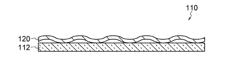
本開示の積層体の一例が図1に模式的に示される。図1に示されるように、本開示の積層体10は、キャリア12と、密着層14と、剥離補助層16と、剥離層18と、金属層20とをこの順に備えたものである。密着層14は、負の標準電極電位を有する金属M1を含む層であり、キャリア12上に設けられる。剥離補助層16は、金属M2を含む層であり、密着層14のキャリア12とは反対の面側に設けられる。M2は、アルカリ金属及びアルカリ土類金属以外の金属である。なお、M1及びM2は互いに異なる金属であるのが好ましい。剥離層18は、剥離補助層16の密着層14とは反対の面側に設けられる。金属層20は、剥離層18の剥離補助層16とは反対の面側に設けられる。そして、本開示の積層体10は、密着層14の厚さT1に対する剥離補助層16の厚さT2の比であるT2/T1が1を超え20以下である。所望により、積層体10における金属層20は、1層から構成される単層であってもよく、2層以上から構成される多層であってもよい。また、キャリア12の両面に上下対称となるように上述の各種層を順に備えてなる構成としてもよい。なお、本開示の積層体10は、あらゆる用途に使用され、特にプリント配線板製造用のキャリア付銅箔として使用されることが好ましい。
本開示による積層体10は、キャリア12を用意し、キャリア12上に、密着層14、剥離補助層16、剥離層18、及び金属層20を形成することにより製造することができる。密着層14、剥離補助層16、剥離層18、及び金属層20の各層の形成は、極薄化によるファインピッチ化に対応しやすい観点から、物理気相堆積(PVD)法により行われるのが好ましい。物理気相堆積(PVD)法の例としては、スパッタリング法、真空蒸着法、及びイオンプレーティング法が挙げられる。中でも、0.05nm以上5000nm以下の幅広い範囲で膜厚制御できる点、広い幅ないし面積にわたって膜厚均一性を確保できる点等から、スパッタリング法を用いることが好ましい。特に、密着層14、剥離補助層16、剥離層18、及び金属層20の全ての層をスパッタリング法により形成することで、製造効率を格段に高くすることができる。物理気相堆積(PVD)法による成膜は公知の気相成膜装置を用いて公知の条件に従って行えばよく特に限定されない。例えば、スパッタリング法を採用する場合、スパッタリング方式としては、例えば、マグネトロンスパッタリング法、2極スパッタリング法、対向ターゲットスパッタリング法等、公知の種々の方式が挙げられる。中でも、マグネトロンスパッタリング法が、成膜速度が速く生産性が高い点で好ましい。スパッタリング法はDC(直流)及びRF(高周波)のいずれの電源で行ってもよい。また、スパッタリング法においては、例えば、ターゲット形状も広く知られているプレート型ターゲットを使用することができる。中でも、ターゲット使用効率の観点から円筒形ターゲットを使用することが望ましい。以下、密着層14、剥離補助層16、剥離層18、及び金属層20の各層の物理気相堆積(PVD)法による成膜について説明する。なお、金属層20は、第1金属層及び第2金属層の2層構成の例として説明する。
図1に示されるように、キャリア12上に、密着層14、剥離補助層16、剥離層18及び金属層20(第1金属層及び第2金属層)をこの順に成膜して積層体10を製造した。具体的な手順は以下のとおりである。
キャリア12として厚さ1.1mmのガラスシート(材質:ソーダライムガラス、算術平均粗さRa:0.6nm、セントラル硝子株式会社製)を用意した。
キャリア12上に、密着層14として厚さ100nmのチタン層をスパッタリング法により形成した。このスパッタリングは以下の装置を用いて以下の条件で行った。
・装置:枚葉式マグネトロンスパッタリング装置(キヤノントッキ株式会社製、MLS464)
・ターゲット:直径8インチ(203.2mm)のチタンターゲット(純度99.999%)
・到達真空度:1×10⁻⁴Pa未満
・スパッタリング圧:0.35Pa
・スパッタリング電力:1000W(3.1W/cm2)
・成膜時温度:40℃
密着層14のキャリア12とは反対の面側に、剥離補助層16として厚さ100nmの銅層をスパッタリング法により形成した。このスパッタリングは以下の装置を用いて以下の条件で行った。
・装置:枚葉式DCスパッタリング装置(キヤノントッキ株式会社製、MLS464)
・ターゲット:直径8インチ(203.2mm)の銅ターゲット(純度99.98%)
・到達真空度:1×10⁻⁴Pa未満
・ガス:アルゴンガス(流量:100sccm)
・スパッタリング圧:0.35Pa
・スパッタリング電力:1000W(6.2W/cm2)
・成膜時温度:40℃
剥離補助層16の密着層14とは反対の面側に、剥離層18として厚み6nmのアモルファスカーボン層をスパッタリング法により形成した。このスパッタリングは以下の装置を用いて以下の条件で行った。
・装置:枚葉式DCスパッタリング装置(キヤノントッキ株式会社製、MLS464)
・ターゲット:直径8インチ(203.2mm)の炭素ターゲット(純度99.999%)
・到達真空度:1×10⁻⁴Pa未満
・ガス:アルゴンガス(流量:100sccm)
・スパッタリング圧:0.35Pa
・スパッタリング電力:250W(0.7W/cm2)
・成膜時温度:40℃
剥離層18の剥離補助層16とは反対の面側に、第1金属層として厚さ100nmのチタン層を以下の装置及び条件でスパッタリングにより形成した。
・装置:枚葉式DCスパッタリング装置(キヤノントッキ株式会社製、MLS464)
・ターゲット:直径8インチ(203.2mm)のチタンターゲット(純度99.999%)
・キャリアガス:アルゴンガス(流量:100sccm)
・到達真空度:1×10⁻⁴Pa未満
・スパッタリング圧:0.35Pa
・スパッタリング電力:1000W(3.1W/cm2)
第1金属層の剥離層18とは反対の面側に、第2金属層として厚さ300nmの銅層をスパッタリング法により形成した。このスパッタリングは以下の装置を用いて以下の条件で行った。
・ターゲット:直径8インチ(203.2mm)の銅ターゲット(純度99.98%)
・到達真空度:1×10⁻⁴Pa未満
・ガス:アルゴンガス(流量:100sccm)
・スパッタリング圧:0.35Pa
・スパッタリング電力:1000W(3.1W/cm2)
・成膜時温度:40℃
密着層14及び剥離補助層16を、1<T2/T1≦20を満たすように表1に示される厚さで形成したこと以外は、例1と同様にして積層体10を製造した。
例1から例11までの積層体について、以下に示されるとおり、剥離強度の測定を行った。評価結果は表1に示されるとおりであった。また、表1には密着層14の厚さT1、剥離補助層16の厚さT2、及びT2/T1も併せて示してある。
積層体10における熱履歴としての真空熱プレスを行った後の剥離強度を測定した。具体的には、積層体10の金属層20側に、厚さ18μmのパネル電解銅めっきを施して銅めっき層を形成して、剥離性評価用サンプルとした。剥離性評価用サンプルは各例につき複数個作製した。これらの剥離性評価用サンプルに対して、熱履歴として表1に示されるように240℃、260℃、280℃、320℃及び340℃のいずれかの温度にて30kgf/cm2の圧力で2時間プレスした。熱プレス後の各剥離性評価用サンプルに対して、JIS C 6481-1996に準拠して、金属層20と一体となった上記電解銅めっき層を剥離したときの剥離強度(gf/cm)を測定した。このとき、測定幅は50mmとし、測定長さは20mmとした。得られた剥離強度(平均値)を以下の基準により格付け評価し、全てのプレス温度において評価Dが一つも無い場合は合格、それ以外の場合は不合格と判定した。
‐評価A:剥離強度が3gf/cm以上30gf/cm未満
‐評価B-:剥離強度が1gf/cm以上3gf/cm未満
‐評価B+:剥離強度が30gf/cm以上100gf/cm未満
‐評価C-:剥離強度が0.5gf/cm以上1gf/cm未満
‐評価C+:剥離強度が100gf/cm以上200gf/cm未満
‐評価D:剥離強度が0.5gf/cm未満又は200gf/cm超(剥離不可を含む)

Claims (5)
- キャリアと、
前記キャリア上に設けられ、負の標準電極電位を有する金属M1を含む密着層と、
前記密着層の前記キャリアとは反対の面側に設けられ、金属M2(M2は、アルカリ金属及びアルカリ土類金属以外の金属である)を含む剥離補助層と、
前記剥離補助層の前記密着層とは反対の面側に設けられる剥離層と、
前記剥離層の前記剥離補助層とは反対の面側に設けられる金属層と、
を備え、
前記密着層の厚さT1に対する前記剥離補助層の厚さT2の比であるT2/T1が1を超え20以下である、積層体。 - 240℃以上340℃以下の任意の温度条件下において、30kgf/cm2の圧力にて2時間プレスする熱履歴を前記積層体に与えた場合に、JIS C6481-1996に準拠して測定される、前記剥離層と前記剥離補助層との間の剥離強度が1gf/cm以上100gf/cm未満である、請求項1に記載の積層体。
- 前記M1がチタンであり、かつ、前記M2が銅である、請求項1又は請求項2に記載の積層体。
- 前記剥離層が炭素を含む、請求項1から請求項3までのいずれか一項に記載の積層体。
- 前記キャリアが、ガラス又はセラミックスで構成される、請求項1から請求項4までのいずれか一項に記載の積層体。
Priority Applications (5)
| Application Number | Priority Date | Filing Date | Title |
|---|---|---|---|
| CN201980073928.3A CN112969581B (zh) | 2018-11-20 | 2019-11-14 | 层叠体 |
| US17/292,492 US12058819B2 (en) | 2018-11-20 | 2019-11-14 | Multilayer body |
| KR1020217007079A KR20210042141A (ko) | 2018-11-20 | 2019-11-14 | 적층체 |
| KR1020237018003A KR102803816B1 (ko) | 2018-11-20 | 2019-11-14 | 적층체 |
| JP2020558332A JP7090176B2 (ja) | 2018-11-20 | 2019-11-14 | 積層体 |
Applications Claiming Priority (4)
| Application Number | Priority Date | Filing Date | Title |
|---|---|---|---|
| JP2018217756 | 2018-11-20 | ||
| JP2018-217756 | 2018-11-20 | ||
| JP2019118303 | 2019-06-26 | ||
| JP2019-118303 | 2019-06-26 |
Publications (1)
| Publication Number | Publication Date |
|---|---|
| WO2020105535A1 true WO2020105535A1 (ja) | 2020-05-28 |
Family
ID=70773069
Family Applications (1)
| Application Number | Title | Priority Date | Filing Date |
|---|---|---|---|
| PCT/JP2019/044663 Ceased WO2020105535A1 (ja) | 2018-11-20 | 2019-11-14 | 積層体 |
Country Status (6)
| Country | Link |
|---|---|
| US (1) | US12058819B2 (ja) |
| JP (1) | JP7090176B2 (ja) |
| KR (2) | KR20210042141A (ja) |
| CN (1) | CN112969581B (ja) |
| TW (2) | TW202237388A (ja) |
| WO (1) | WO2020105535A1 (ja) |
Families Citing this family (4)
| Publication number | Priority date | Publication date | Assignee | Title |
|---|---|---|---|---|
| CN114178710B (zh) * | 2020-08-24 | 2024-11-26 | 奥特斯(中国)有限公司 | 部件承载件及其制造方法 |
| TWI765366B (zh) * | 2020-10-06 | 2022-05-21 | 昂筠國際股份有限公司 | 附金屬載體及其製造方法 |
| KR20260024341A (ko) * | 2024-08-13 | 2026-02-20 | 앱솔릭스 인코포레이티드 | 패키징 기판 및 이를 포함하는 반도체 패키지 |
| CN120534047B (zh) * | 2025-06-18 | 2025-12-02 | 北京魁冠科技有限公司 | 带载体金属箔及覆金属层叠板 |
Citations (4)
| Publication number | Priority date | Publication date | Assignee | Title |
|---|---|---|---|---|
| JP2007307767A (ja) * | 2006-05-17 | 2007-11-29 | Mitsui Mining & Smelting Co Ltd | キャリア箔付銅箔、キャリア箔付銅箔の製造方法、キャリア箔付表面処理銅箔及びそのキャリア箔付表面処理銅箔を用いた銅張積層板 |
| JP5859155B1 (ja) * | 2015-03-11 | 2016-02-10 | 福田金属箔粉工業株式会社 | 複合金属箔及びその製造方法並びにプリント配線板 |
| WO2017149811A1 (ja) * | 2016-02-29 | 2017-09-08 | 三井金属鉱業株式会社 | キャリア付銅箔、並びに配線層付コアレス支持体及びプリント配線板の製造方法 |
| JP2017228693A (ja) * | 2016-06-23 | 2017-12-28 | 三菱マテリアル株式会社 | 接合体、パワーモジュール用基板、接合体の製造方法、及び、パワーモジュール用基板の製造方法 |
Family Cites Families (4)
| Publication number | Priority date | Publication date | Assignee | Title |
|---|---|---|---|---|
| JPS5859155U (ja) | 1981-10-19 | 1983-04-21 | 電気音響株式会社 | 偏向ヨ−ク |
| JP2000340911A (ja) * | 1999-05-25 | 2000-12-08 | Mitsui Mining & Smelting Co Ltd | プリント配線板用銅箔 |
| US7026059B2 (en) | 2000-09-22 | 2006-04-11 | Circuit Foil Japan Co., Ltd. | Copper foil for high-density ultrafine printed wiring boad |
| JP4273895B2 (ja) | 2003-09-24 | 2009-06-03 | 日立化成工業株式会社 | 半導体素子搭載用パッケージ基板の製造方法 |
-
2019
- 2019-11-14 JP JP2020558332A patent/JP7090176B2/ja active Active
- 2019-11-14 US US17/292,492 patent/US12058819B2/en active Active
- 2019-11-14 KR KR1020217007079A patent/KR20210042141A/ko not_active Ceased
- 2019-11-14 KR KR1020237018003A patent/KR102803816B1/ko active Active
- 2019-11-14 WO PCT/JP2019/044663 patent/WO2020105535A1/ja not_active Ceased
- 2019-11-14 CN CN201980073928.3A patent/CN112969581B/zh active Active
- 2019-11-19 TW TW111122344A patent/TW202237388A/zh unknown
- 2019-11-19 TW TW108141876A patent/TWI783190B/zh active
Patent Citations (4)
| Publication number | Priority date | Publication date | Assignee | Title |
|---|---|---|---|---|
| JP2007307767A (ja) * | 2006-05-17 | 2007-11-29 | Mitsui Mining & Smelting Co Ltd | キャリア箔付銅箔、キャリア箔付銅箔の製造方法、キャリア箔付表面処理銅箔及びそのキャリア箔付表面処理銅箔を用いた銅張積層板 |
| JP5859155B1 (ja) * | 2015-03-11 | 2016-02-10 | 福田金属箔粉工業株式会社 | 複合金属箔及びその製造方法並びにプリント配線板 |
| WO2017149811A1 (ja) * | 2016-02-29 | 2017-09-08 | 三井金属鉱業株式会社 | キャリア付銅箔、並びに配線層付コアレス支持体及びプリント配線板の製造方法 |
| JP2017228693A (ja) * | 2016-06-23 | 2017-12-28 | 三菱マテリアル株式会社 | 接合体、パワーモジュール用基板、接合体の製造方法、及び、パワーモジュール用基板の製造方法 |
Also Published As
| Publication number | Publication date |
|---|---|
| KR20210042141A (ko) | 2021-04-16 |
| US12058819B2 (en) | 2024-08-06 |
| TW202027979A (zh) | 2020-08-01 |
| TW202237388A (zh) | 2022-10-01 |
| US20220022326A1 (en) | 2022-01-20 |
| CN112969581A (zh) | 2021-06-15 |
| JPWO2020105535A1 (ja) | 2021-09-02 |
| TWI783190B (zh) | 2022-11-11 |
| KR20230080499A (ko) | 2023-06-07 |
| CN112969581B (zh) | 2023-08-11 |
| KR102803816B1 (ko) | 2025-05-08 |
| JP7090176B2 (ja) | 2022-06-23 |
Similar Documents
| Publication | Publication Date | Title |
|---|---|---|
| US10888003B2 (en) | Copper foil with carrier, coreless support with wiring layer, and method for producing printed circuit board | |
| JP7090176B2 (ja) | 積層体 | |
| JP2023033313A (ja) | キャリア付銅箔 | |
| JP2024061811A (ja) | キャリア付金属箔 | |
| JP7336559B2 (ja) | 積層体 | |
| US12193153B2 (en) | Multilayer body |
Legal Events
| Date | Code | Title | Description |
|---|---|---|---|
| 121 | Ep: the epo has been informed by wipo that ep was designated in this application |
Ref document number: 19887556 Country of ref document: EP Kind code of ref document: A1 |
|
| ENP | Entry into the national phase |
Ref document number: 2020558332 Country of ref document: JP Kind code of ref document: A |
|
| NENP | Non-entry into the national phase |
Ref country code: DE |
|
| 122 | Ep: pct application non-entry in european phase |
Ref document number: 19887556 Country of ref document: EP Kind code of ref document: A1 |
|
| WWC | Wipo information: continuation of processing after refusal or withdrawal |
Ref document number: 1020237018003 Country of ref document: KR |