WO2020100441A1 - 表示装置、及びその製造方法 - Google Patents
表示装置、及びその製造方法 Download PDFInfo
- Publication number
- WO2020100441A1 WO2020100441A1 PCT/JP2019/037575 JP2019037575W WO2020100441A1 WO 2020100441 A1 WO2020100441 A1 WO 2020100441A1 JP 2019037575 W JP2019037575 W JP 2019037575W WO 2020100441 A1 WO2020100441 A1 WO 2020100441A1
- Authority
- WO
- WIPO (PCT)
- Prior art keywords
- pixel
- vapor deposition
- convex portion
- deposition mask
- substrate
- Prior art date
- Legal status (The legal status is an assumption and is not a legal conclusion. Google has not performed a legal analysis and makes no representation as to the accuracy of the status listed.)
- Ceased
Links
Images


Classifications
-
- H—ELECTRICITY
- H10—SEMICONDUCTOR DEVICES; ELECTRIC SOLID-STATE DEVICES NOT OTHERWISE PROVIDED FOR
- H10K—ORGANIC ELECTRIC SOLID-STATE DEVICES
- H10K59/00—Integrated devices, or assemblies of multiple devices, comprising at least one organic light-emitting element covered by group H10K50/00
- H10K59/30—Devices specially adapted for multicolour light emission
- H10K59/35—Devices specially adapted for multicolour light emission comprising red-green-blue [RGB] subpixels
-
- G—PHYSICS
- G09—EDUCATION; CRYPTOGRAPHY; DISPLAY; ADVERTISING; SEALS
- G09F—DISPLAYING; ADVERTISING; SIGNS; LABELS OR NAME-PLATES; SEALS
- G09F9/00—Indicating arrangements for variable information in which the information is built-up on a support by selection or combination of individual elements
- G09F9/30—Indicating arrangements for variable information in which the information is built-up on a support by selection or combination of individual elements in which the desired character or characters are formed by combining individual elements
-
- H—ELECTRICITY
- H05—ELECTRIC TECHNIQUES NOT OTHERWISE PROVIDED FOR
- H05B—ELECTRIC HEATING; ELECTRIC LIGHT SOURCES NOT OTHERWISE PROVIDED FOR; CIRCUIT ARRANGEMENTS FOR ELECTRIC LIGHT SOURCES, IN GENERAL
- H05B33/00—Electroluminescent light sources
- H05B33/10—Apparatus or processes specially adapted to the manufacture of electroluminescent light sources
-
- H—ELECTRICITY
- H05—ELECTRIC TECHNIQUES NOT OTHERWISE PROVIDED FOR
- H05B—ELECTRIC HEATING; ELECTRIC LIGHT SOURCES NOT OTHERWISE PROVIDED FOR; CIRCUIT ARRANGEMENTS FOR ELECTRIC LIGHT SOURCES, IN GENERAL
- H05B33/00—Electroluminescent light sources
- H05B33/12—Light sources with substantially two-dimensional radiating surfaces
- H05B33/22—Light sources with substantially two-dimensional radiating surfaces characterised by the chemical or physical composition or the arrangement of auxiliary dielectric or reflective layers
-
- H—ELECTRICITY
- H05—ELECTRIC TECHNIQUES NOT OTHERWISE PROVIDED FOR
- H05B—ELECTRIC HEATING; ELECTRIC LIGHT SOURCES NOT OTHERWISE PROVIDED FOR; CIRCUIT ARRANGEMENTS FOR ELECTRIC LIGHT SOURCES, IN GENERAL
- H05B33/00—Electroluminescent light sources
- H05B33/12—Light sources with substantially two-dimensional radiating surfaces
- H05B33/26—Light sources with substantially two-dimensional radiating surfaces characterised by the composition or arrangement of the conductive material used as an electrode
-
- H—ELECTRICITY
- H10—SEMICONDUCTOR DEVICES; ELECTRIC SOLID-STATE DEVICES NOT OTHERWISE PROVIDED FOR
- H10K—ORGANIC ELECTRIC SOLID-STATE DEVICES
- H10K50/00—Organic light-emitting devices
- H10K50/10—OLEDs or polymer light-emitting diodes [PLED]
- H10K50/11—OLEDs or polymer light-emitting diodes [PLED] characterised by the electroluminescent [EL] layers
- H10K50/125—OLEDs or polymer light-emitting diodes [PLED] characterised by the electroluminescent [EL] layers specially adapted for multicolour light emission, e.g. for emitting white light
-
- H—ELECTRICITY
- H10—SEMICONDUCTOR DEVICES; ELECTRIC SOLID-STATE DEVICES NOT OTHERWISE PROVIDED FOR
- H10K—ORGANIC ELECTRIC SOLID-STATE DEVICES
- H10K59/00—Integrated devices, or assemblies of multiple devices, comprising at least one organic light-emitting element covered by group H10K50/00
- H10K59/10—OLED displays
- H10K59/12—Active-matrix OLED [AMOLED] displays
- H10K59/1201—Manufacture or treatment
-
- H—ELECTRICITY
- H10—SEMICONDUCTOR DEVICES; ELECTRIC SOLID-STATE DEVICES NOT OTHERWISE PROVIDED FOR
- H10K—ORGANIC ELECTRIC SOLID-STATE DEVICES
- H10K59/00—Integrated devices, or assemblies of multiple devices, comprising at least one organic light-emitting element covered by group H10K50/00
- H10K59/10—OLED displays
- H10K59/12—Active-matrix OLED [AMOLED] displays
- H10K59/122—Pixel-defining structures or layers, e.g. banks
-
- H—ELECTRICITY
- H10—SEMICONDUCTOR DEVICES; ELECTRIC SOLID-STATE DEVICES NOT OTHERWISE PROVIDED FOR
- H10K—ORGANIC ELECTRIC SOLID-STATE DEVICES
- H10K59/00—Integrated devices, or assemblies of multiple devices, comprising at least one organic light-emitting element covered by group H10K50/00
- H10K59/30—Devices specially adapted for multicolour light emission
- H10K59/35—Devices specially adapted for multicolour light emission comprising red-green-blue [RGB] subpixels
- H10K59/352—Devices specially adapted for multicolour light emission comprising red-green-blue [RGB] subpixels the areas of the RGB subpixels being different
-
- H—ELECTRICITY
- H10—SEMICONDUCTOR DEVICES; ELECTRIC SOLID-STATE DEVICES NOT OTHERWISE PROVIDED FOR
- H10K—ORGANIC ELECTRIC SOLID-STATE DEVICES
- H10K71/00—Manufacture or treatment specially adapted for the organic devices covered by this subclass
-
- H—ELECTRICITY
- H10—SEMICONDUCTOR DEVICES; ELECTRIC SOLID-STATE DEVICES NOT OTHERWISE PROVIDED FOR
- H10K—ORGANIC ELECTRIC SOLID-STATE DEVICES
- H10K71/00—Manufacture or treatment specially adapted for the organic devices covered by this subclass
- H10K71/10—Deposition of organic active material
- H10K71/16—Deposition of organic active material using physical vapour deposition [PVD], e.g. vacuum deposition or sputtering
- H10K71/166—Deposition of organic active material using physical vapour deposition [PVD], e.g. vacuum deposition or sputtering using selective deposition, e.g. using a mask
Definitions
- the present invention relates to a display device and a manufacturing method thereof.
- organic EL display devices which are display devices using organic electroluminescence (EL) elements
- An organic EL element is generally called an OLED (organic light emitting diode)
- an organic EL display device uses light emitted from the OLED to generate a plurality of colors such as red (R), green (G), and blue (B), and color.
- Display the image Each pixel arranged two-dimensionally in the image display area is composed of a plurality of types of sub-pixels that emit light of different colors. The emission intensity of each sub-pixel can be controlled independently, and the pixel can express various colors according to the balance of the emission intensity.
- RGB the material of the light emitting layer of the OLED is separately applied in accordance with the color of the sub-pixel to make the light emitting color of the OLED different. Therefore, this structure is called an RGB painting method or the like.
- a vapor deposition mask is arranged as a shadow mask on a substrate and a light emitting layer is vapor deposited in the opening.
- One of the countermeasures is to arrange a spacer for securing the distance between the substrate and the vapor deposition mask, but if the distance between the substrate and the vapor deposition mask is widened, a side effect of degrading the vapor deposition position accuracy also occurs.
- the present invention has been made to solve the above problems, and an object of the present invention is to improve the accuracy of vapor deposition position and reduce the possibility of occurrence of display defects in a display device in which an OLED is formed by a separate coating method. To do.
- a display device includes a substrate on which a display unit for displaying an image including a plurality of pixels is formed, a first pixel electrode provided on the surface of the substrate corresponding to each pixel, The first pixel electrode, the first convex portion and the second convex portion of the surface of the substrate provided in the boundary region between the pixels, respectively, and a layer exhibiting a first emission color, A first organic layer laminated on the pixel electrode, and a second organic layer laminated on the second pixel electrode including a layer exhibiting a second emission color, the first organic layer Is further provided so as to cover only the first convex portion among the convex portions, and the second organic layer is provided so as not to cover both the first convex portion and the second convex portion. ing.
- a method for manufacturing a display device is a substrate on which a display unit for displaying an image composed of a plurality of pixels is formed, and the substrate is provided on the surface of the substrate so as to correspond to the pixels.
- a first vapor deposition mask having an opening in a region facing the pixel electrode and the first convex portion and having a shielding portion in a region facing the second convex portion on the substrate.
- the first pixel electrode and the first convex portion are covered so as not to cover the second convex portion.
- a second vapor deposition mask having a shielding portion in a region facing the second vapor deposition mask on the substrate, and a vapor deposition process through the second vapor deposition mask to cover the second pixel electrode, and And a step of forming a second organic layer including a layer exhibiting a second emission color so as not to cover the first convex portion and the second convex portion.
- FIG. 3 is a schematic plan view of a display panel of the organic EL display device according to the first embodiment of the present invention.
- FIG. 3 is a schematic vertical sectional view of the array substrate at a position along line IIIa-IIIa and line IIIb-IIIb shown in FIG. 2.
- FIG. 3 is a schematic partial plan view of the array substrate in a state after the bank is formed and before the organic material layer is formed in the first embodiment of the present invention.
- FIG. 5 is a schematic vertical sectional view taken along lines Va-Va and Vb-Vb of the array substrate of FIG. 4.
- FIG. 5 is a schematic partial plan view of an array substrate corresponding to FIG. 4 after an organic material layer is formed.
- FIG. 5 is a schematic plan view of a vapor deposition mask for B arranged on the array substrate shown in FIG. 4. It is a typical vertical sectional view of an array substrate and a vapor deposition mask in the state where the organic material layer of B pixel was vapor deposited.
- FIG. 5 is a schematic plan view of a vapor deposition mask for G arranged on the array substrate shown in FIG. 4.
- FIG. 3 is a schematic vertical sectional view of an array substrate and a vapor deposition mask in a state where an organic material layer of G pixels is vapor deposited.
- FIG. 5 is a schematic partial plan view of an array substrate corresponding to FIG. 4 after an organic material layer is formed.
- FIG. 5 is a schematic plan view of a vapor deposition mask for B arranged on the array substrate shown in FIG. 4. It is a typical vertical sectional view of an array substrate and a vapor
- FIG. 5 is a schematic plan view of a vapor deposition mask for R arranged on the array substrate shown in FIG. 4.
- FIG. 3 is a schematic vertical cross-sectional view of an array substrate and a vapor deposition mask in a state where an organic material layer for R pixels is vapor deposited.
- FIG. 9 is a schematic partial plan view of an array substrate in a state after an organic material layer is formed in the second embodiment of the present invention. It is a typical top view of the vapor deposition mask for B arranged on the array substrate in a 2nd embodiment of the present invention. It is a typical top view of the vapor deposition mask for R arranged on the array substrate in a 2nd embodiment of the present invention.
- FIG. 19 is a schematic partial plan view of the array substrate of FIG. 18 after the organic material layer is formed.
- the embodiment described below is an organic EL display device.
- the organic EL display device is an active matrix type display device and is mounted on a television, a personal computer, a mobile terminal, a mobile phone, and the like.
- a plurality of pixels forming an image are two-dimensionally arranged in the image display area of the display device.
- the xyz coordinate system which is a three-dimensional orthogonal coordinate system
- the x-axis and the y-axis are set corresponding to the two-dimensional orthogonal coordinate system corresponding to the image.
- the x-axis is the horizontal direction of the image and the y-axis is the vertical method of the image.
- the z axis is in the thickness direction of the array substrate described later.
- a display device capable of displaying a color image by arranging a plurality of types of pixels (sub-pixels) having different emission colors in the image display area
- the emission colors are RGB three colors.
- a pixel in a color image corresponds to a set of subpixel groups including a plurality of types of subpixels in a display device.
- a subpixel is a structural unit, and an OLED or a pixel circuit is provided for each subpixel. Is formed. Therefore, in the following description, the sub-pixel is basically treated as a pixel.
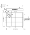
- FIG. 1 is a schematic diagram showing a schematic configuration of an organic EL display device 2 according to the embodiment.
- the organic EL display device 2 includes a pixel array unit 4 that is a display unit that displays an image, and a drive unit that drives the pixel array unit.
- the organic EL display device 2 has a laminated structure such as thin film transistors (TFTs) and OLEDs formed on a substrate made of a glass substrate or a flexible resin film.
- TFTs thin film transistors
- OLEDs formed on a substrate made of a glass substrate or a flexible resin film.
- OLEDs 6 and pixel circuits 8 are arranged in a matrix corresponding to the pixels.
- the pixel circuit 8 is composed of a plurality of TFTs and capacitors.
- the pixel circuit 8 shown in FIG. 1 exemplifies a simplified configuration including TFTs 10 and 12 and a capacitor 14.
- the driving unit includes a scanning line driving circuit 20, a video line driving circuit 22, a driving power supply circuit 24, a reference power supply circuit 26, and a control device 28, and has a function of driving the pixel circuit 8 and controlling light emission of the OLED 6. ..
- the scanning line drive circuit 20 is connected to a scanning signal line 30 provided for each horizontal arrangement (pixel row) of pixels.
- the scanning line drive circuit 20 sequentially selects the scanning signal lines 30 according to the timing signal input from the control device 28, and applies a voltage for turning on the switching TFT 10 to the selected scanning signal lines 30.
- the video line drive circuit 22 is connected to a video signal line 32 provided for each vertical arrangement of pixels (pixel column).
- the video line driving circuit 22 receives a video signal from the control device 28, and according to the selection of the scanning signal line 30 by the scanning line driving circuit 20, a voltage corresponding to the video signal of the selected pixel row is applied to each video signal line 32. Output to.
- the voltage is written in the capacitor 14 via the switching TFT 10 in the selected pixel row.
- the drive TFT 12 supplies a current according to the written voltage to the OLED 6, whereby the OLED 6 of the pixel corresponding to the selected scanning signal line 30 emits light.
- the drive power supply circuit 24 is connected to the drive power supply line 34 provided for each pixel column, and supplies a current to the OLED 6 via the drive power supply line 34 and the drive TFT 12 of the selected pixel row.
- the reference power supply circuit 26 applies a constant potential ⁇ REF to a common electrode (not shown) that constitutes the cathode electrode of the OLED 6.
- the lower electrode of the OLED 6 is a pixel electrode formed for each pixel, and the upper electrode of the OLED 6 is a common electrode commonly arranged so as to cover a plurality of pixel electrodes.
- the lower electrode is connected to the driving TFT 12.
- the upper electrode is an electrode common to the OLEDs 6 of all pixels.
- the lower electrode is the anode (anode) of the OLED 6 and the upper electrode is the cathode (cathode).
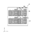
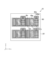
- FIG. 2 is a schematic plan view of the display panel 40 of the organic EL display device 2.
- the display panel 40 has a rectangular shape, and has a structure in which, for example, an array substrate 41 and a counter substrate are bonded together with a filling material interposed therebetween.
- the array substrate 41 includes a display area 42, a frame area 44, and a connection terminal area 46.
- the pixel array section 4 shown in FIG. 1 is provided in the display area 42, and the OLED 6 and the pixel circuit 8 are formed in the pixel array section 4 as described above. Meanwhile, a polarizing plate or a touch panel may be provided on the counter substrate.
- the frame area 44 is the outer edge area of the display area 42, the inner boundary matches the contour of the display area 42, the outer boundary is a rectangle, three sides of which overlap the sides of the display panel 40, and the remaining one side is connected. It becomes a boundary with the terminal region 46.
- the end of the display area 42 is defined as the end of the light emitting area of the OLED 6 belonging to the outermost pixel, the pixel circuit 8 is provided so as to straddle the boundary between the display area 42 and the frame area 44. In some cases.
- connection terminal area 46 is provided adjacent to the frame area 44.
- the connection terminal area 46 has a rectangular shape in which three sides overlap the sides of the display panel 40 and the remaining one side is a boundary with the frame area 44.
- Wirings for inputting and outputting electric signals necessary for the operation of the pixel array section 4 formed in the display region 42 are drawn from the display region 42 and the frame region 44 to the connection terminal region 46. That is, a group of wirings drawn from the display area 42 and the frame area 44 is arranged in the connection terminal area 46.
- connection terminals for connecting the wiring group to an external circuit are arranged.
- a plurality of connection terminals are arranged, one of which is connected to one of a group of wirings drawn from the display area 42 and the frame area 44.
- the FPC 48 is connected to the connection terminal
- the FPC 48 is connected to the control device 28 and other circuits 20, 22, 24, 26, etc., or the IC 50 is mounted thereon.
- the display panel 40 of the present embodiment displays a color image, and the pixels in the color image are composed of pixels (sub-pixels) that emit light corresponding to any of the three colors of RGB, for example.
- R pixels 52r, G pixels 52g, and B pixels 52b are arranged in stripes in the display area.
- pixels of the same type (color) are arranged in the y direction of the image, and RGB are arranged periodically in the x direction.
- the R pixel 52r, the G pixel 52g, and the B pixel 52b each schematically show an effective light emitting region, structurally correspond to the pixel opening 60, and the region between them is a bank 84 described later. It corresponds to.
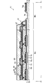
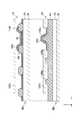
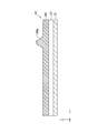
- FIG. 3 is a schematic vertical cross-sectional view of the array substrate 41, and a cross-section IIIa is a cross-section in the display region 42 at a position along the line IIIa-IIIa shown in FIG.
- a cross section IIIb is a cross section taken along the line IIIb-IIIb shown in FIG. 2, and is a cross section of the connection terminal region 46 and the frame region 44 adjacent thereto.
- the substrate 70 is made of a flexible film such as polyimide or polyethylene terephthalate.
- the substrate 70 can also be formed of other resin or glass.
- An undercoat layer 71 which serves as a barrier against impurities contained in the substrate 70, is formed on the surface of the substrate 70.
- the undercoat layer 71 is made of a silicon oxide film, a silicon nitride film, or the like, and may have a laminated structure of them.
- a semiconductor layer 72 is laminated on the undercoat layer 71, and the semiconductor layer 72 forms a channel region, a source region, and a drain region of a TFT 73 such as a pixel circuit.
- the gate insulating film 75 is formed of silicon oxide or the like, and the metal film laminated thereon is patterned to form the gate electrode 76 of the TFT.
- An inorganic film 77 is laminated as an interlayer insulating film so as to cover the gate electrode 76 and the like.
- a metal film is formed on the inorganic film 77, and the S / D (source / drain) electrodes 78s and 78d of the TFT are formed using the metal film.
- the S / D electrodes 78s and 78d are electrically connected to the semiconductor layer 72 of the TFT through a contact hole penetrating the gate insulating film 75 and the inorganic film 77.
- a region including a connecting portion with the S / D electrode 78s, the region into which an impurity imparting conductivity is injected is used as a source region, and a connecting portion with the S / D electrode 78d is included.
- the region into which the impurity-imparting impurities are implanted is referred to as a drain region.
- the metal film is a conductive film laminated between the OLED and the substrate 70, and the metal film can be used to form a lower layer wiring located below the OLED.
- the lower layer wiring forms the wiring 79 in the connection terminal region 46 and the connection terminal 79p.
- a flattening film 80 made of an organic material is laminated to cover the inorganic film 77.
- Polyimide, acrylic resin, or the like is used as the flattening film 80.
- the flattening film 80 flattens the surface on which the OLED is formed.
- an inorganic film 81 is formed on the flattening film 80 in order to prevent water from entering the OLED from the flattening film 80 or the like.
- the inorganic film 81 is formed of a material having moisture resistance and insulation.
- the inorganic film 81 is formed using a silicon nitride film or a laminated film of a silicon nitride film and a silicon oxide film.
- the pixel electrode 82 of the OLED is arranged on the surface of the inorganic film 81.
- the pixel electrode 82 is electrically connected to the S / D electrode 78s of the TFT 73 corresponding to the driving TFT 12 of FIG. 1 via a contact hole penetrating the inorganic film 81 and the flattening film 80.
- the pixel electrode 82 may have a structure including a reflective film that reflects the light emitted from the OLED to the display surface side.
- the pixel electrode 82 has a laminated structure of a transparent conductive material such as indium tin oxide (ITO) or indium zinc oxide (IZO) and a reflective material such as silver (Ag). be able to.
- the S / D electrode 78 s connected to the pixel electrode 82 and the source region of the semiconductor layer 72, and the metal layer 76 c located between them and connected to the gate electrode 76 are the storage capacitance shown as the capacitor 14 in FIG. 1.
- the conductive film 83 may be disposed below the pixel electrode 82 with the inorganic film 81 interposed therebetween, and the conductive film 83 may be grounded, for example, to form a storage capacitor with the pixel electrode 82.
- the storage capacitor stabilizes the voltage written in the storage capacitor and contributes to a stable operation of the organic light emitting diode.
- a bank 84 made of an insulating material is formed on the surface of the inorganic film 81 on which the pixel electrode 82 is formed.
- the bank 84 is formed along the periphery of the pixel, covers the end of the pixel electrode 82, and has an opening at the position of the light emitting surface of the OLED.
- the upper surface of the pixel electrode 82 is exposed at the bottom of the opening, and an organic material layer 85 that is an organic layer including a light emitting layer is laminated on the surface.
- the bank 84 is formed of polyimide, acrylic resin, or the like.
- the upper electrode 86 of the OLED is formed on the organic material layer 85.
- the upper electrode 86 can be a common electrode over the entire pixels in the display area.
- the upper electrode 86 is formed of a material that transmits the light emitted from the organic material layer 85.
- the upper electrode 86 is a thin film formed of a metal having a low work function so that electrons can be efficiently injected into the organic material layer 85, and is semitransparent. Is formed to have a film thickness that allows the light to pass therethrough.
- the upper electrode 86 is electrically connected to the wiring 79 via the contact hole 87 provided in the frame region 44 shown in the cross section IIIb.
- a sealing film that seals the upper surface of the OLED and prevents deterioration of the OLED due to moisture is formed in the display area 42 in which the OLED including the pixel electrode 82, the organic material layer 85, and the upper electrode 86 is formed.
- the sealing film is a multilayer film including two inorganic films 88 and 89 and an organic film 90.
- the inorganic films 88 and 89 are formed of, for example, a silicon nitride film, and the organic film 90 is formed of a resin such as acrylic.
- the inorganic film 88 is laminated on the surface of the upper electrode 86 in the display region 42, the organic film 90 is sandwiched between the inorganic film 88 and the inorganic film 89 in the display region 42, and the inorganic films 88 and 89 are frame regions. At 44, there are contact areas that directly contact and overlap each other.
- an inorganic film bonding portion 91 in which the inorganic films 88 and 89 and the inorganic film 81 are bonded is provided.
- the inorganic film bonding portion 91 is basically provided so as to be continuous with the periphery of the display region 42, and thereby water intrusion can be prevented more effectively.
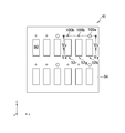
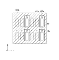
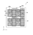
- FIG. 4 is a schematic plan view of a part of the display region 42 of the array substrate 41, showing a state after the bank 84 is formed and before the organic material layer 85 is formed.
- 5 is a schematic vertical cross-sectional view of a part of the array substrate 41 in this state.
- the cross-section Va is a cross-section along the line Va-Va shown in FIG. 4
- the cross-section Vb is the cross-section Vb shown in FIG. It is a cross section taken along line -Vb.
- FIG. 4 a formation region of the bank 84 in the display region 42 and a plurality of pixel openings 60 are shown.
- the plurality of pixel openings 60 are R pixels 52r formed in a stripe array, as in FIG. , G pixel 52g and B pixel 52b.
- the convex portion 100 is formed on the surface of the bank 84.
- the protrusion 100 includes two types of protrusions 100a and 100b having different heights. Specifically, the first protrusion 100a is higher than the second protrusion 100b. That is, if the z-axis is defined such that the z coordinate increases in accordance with the height, the z coordinate of the apex of the first convex portion 100a is larger than the z coordinate of the apex of the second convex portion 100b.
- the first convex portion 100a is basically arranged in the vicinity of a specific one kind of pixel opening 60 among RGB pixels.
- the first convex portion 100a is provided adjacent to each B pixel 52b.
- the second convex portion 100b is arranged adjacent to each R pixel 52r and each G pixel 52g.
- the pixel openings 60 are elongated in the y direction, and the interval in the x direction can be formed smaller than the interval in the y direction. That is, since the bank 84 between the pixels adjacent in the y direction has a width larger than that between the pixels adjacent in the x direction, the convex portion 100 can be easily arranged. Therefore, in this embodiment, the convex portion 100 is arranged on the bank 84 between the pixel rows. That is, the convex portion 100a is provided adjacent to the B pixel 52b in the y direction, and the convex portion 100b is provided adjacent to the R pixel 52r and the G pixel 52g in the y direction.
- the layer 101 forming the array substrate 41 has a laminated structure including the undercoat layer 71 to the inorganic film 81 of FIG.
- the convex portions 100a and 100b are arranged in the x direction on a common straight line, and the convex portions 100a and 100b adjacent to each BGB pixel appear on the cross section Vb at the x coordinate corresponding to the pixel opening 60.
- the height of the upper end of the bank 84 in the cross section Va corresponds to the height of the lower end of the convex portion 100 in the cross section Vb.
- the convex portion 100 is formed of the same material as the bank 84, but it may be formed of a material different from that of the bank 84. That is, when the bank 84 is formed of polyimide or acrylic resin as described above, the convex portion 100 may be formed of the same material as that, for example, another organic material such as epoxy or an inorganic material such as silicon oxynitride. It may be formed of a material.
- the shape of the convex portion 100 is a trapezoid in the vertical cross section and a circular plane shape in the examples of FIGS. 4 and 5, but other shapes may be used.
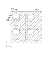
- FIG. 6 is a schematic plan view corresponding to FIG. 4 after formation of the organic material layer 85 in a part of the display area 42 of the array substrate 41.
- the organic material layer 85b is formed in a rectangular region including the pixel electrode 82 exposed on the bottom surface of the pixel opening 60 of the B pixel 52b and its periphery by a manufacturing method described later, and the pixel opening of each of the R pixel 52r and the G pixel 52g.
- Organic material layers 85r and 85g are formed in a rectangular area including the pixel electrode 82 exposed on the bottom surface of the pixel 60 and its periphery.
- the first convex portion 100a is covered by the organic material layer 85b of the adjacent B pixel 52b, but the second convex portion 100b is not covered by the organic material layer 85 of any pixel.
- the organic material layer 85b of the B pixel 52b of the RGB pixels covers only the first convex portion 100a of the convex portions 100a and 100b, and the organic material layers 85r and 85g of the R pixel 52r and the G pixel 52g are It is provided so as to cover neither the first protrusion 100a nor the second protrusion 100b.
- the manufacturing method is basically different from the conventional manufacturing method in that the manufacturing method has a step of forming the convex portion 100 and the method of forming the organic material layer 85.
- the feature of the manufacturing method according to the present invention is mainly in the method of forming the organic material layer 85, particularly in that the organic material layer 85 is formed by utilizing the convex portions 100.
- the convex portion 100 can be formed by, for example, a well-known process similar to or similar to forming the pixel opening 60 in the bank 84, and specifically, a film such as a resin laminated on the surface of the array substrate 41 is formed. It can be made by etching using photolithography technology.
- the three types of organic material layers 85r, 85g, and 85b corresponding to the three emission colors are formed by a separate coating method. Specifically, for each of the three types of organic material layers, a vapor deposition mask having openings corresponding to respective film forming positions is prepared, and the organic material layers 85r, 85g, and 85b are sequentially arranged using the vapor deposition mask. It is vapor-deposited on the surface of the substrate 41.
- the organic material layer 85b is first formed on the B pixel 52b adjacent to the first convex portion 100a, and then the organic material layers 85g and 85r are sequentially formed on the G pixel 52g and the R pixel 52r.
- FIGS. 7 and 8 are diagrams for explaining a forming process of the organic material layer 85b
- FIGS. 9 and 10 are diagrams for explaining a forming process of the organic material layer 85g
- FIGS. 11 and 12 are organic material layers 85r.
- FIG. 6 is a diagram illustrating a forming process of FIG.
- FIGS. 7, 9, and 11 are schematic plan views of vapor deposition masks for B, G, and R, respectively, which are shown in association with the array substrate 41 shown in FIG.
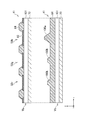
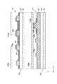
- FIG. 7 is a schematic vertical cross-sectional view of the array substrate 41 and the vapor deposition mask 105b in a state where the organic material layer 85b is vapor-deposited, which is shown in association with the cross-sectional view of FIG. That is, the section VIIIa is a vertical section at a position along the line Va-Va shown in FIG. 4, and the section VIIIb is a vertical section at a position along the line Vb-Vb shown in FIG.
- the opening 110b of the vapor deposition mask 105b for B includes a pixel opening 60 of only the B pixel 52b among the RGB pixels on the array substrate 41, and also includes a first convex portion 100a adjacent to the B pixel 52b. -It is formed into a size. Therefore, when the vapor deposition mask 105b is arranged on the array substrate 41, the first convex portion 100a does not contact the vapor deposition mask 105b and is lower than the first convex portion 100a as shown in a cross section VIIIb of FIG. The upper end of the second convex portion 100b contacts the back surface of the vapor deposition mask 105b and supports the vapor deposition mask 105b.
- the first convex portion 100a does not serve as a spacer that defines the height of the vapor deposition mask 105b on the array substrate 41, and the second convex portion 100b that is lower than the first convex portion 100a functions as the spacer.
- the organic material layer 85b is laminated on the pixel opening 60 of the B pixel 52b as shown in the section VIIIa of FIG. 8 and FIG. 6, and also the section VIIIb of FIG. As shown in 6, the first convex portion 100a is also covered.
- FIG. 10 is a schematic vertical cross-sectional view of the array substrate 41 and the vapor deposition mask 105g in a state where the organic material layer 85g is vapor-deposited, which is shown in association with the cross-sectional view of FIG. That is, the section Xa is a vertical section at a position along the line Va-Va shown in FIG. 4, and the section Xb is a vertical section at a position along the line Vb-Vb shown in FIG.
- the opening 110g of the vapor deposition mask 105g for G is formed on the array substrate 41 in a shape and size that includes the pixel opening 60 of only the G pixel 52g of the RGB pixels, but does not include any of the protrusions 100. ing. Therefore, when the vapor deposition mask 105g is arranged on the array substrate 41, the upper end of the first convex portion 100a higher than the second convex portion 100b comes into contact with the back surface of the vapor deposition mask 105g as shown in the cross section Xb of FIG. Then, the vapor deposition mask 105g is supported. That is, the first convex portion 100a functions as a spacer that defines the height of the vapor deposition mask 105g on the array substrate 41.
- the organic material layer 85g is laminated on the pixel opening 60 of the G pixel 52g as shown in the cross section Xa of FIG. 10 and FIG.
- the organic material layer 85g does not cover either the first protrusion 100a or the second protrusion 100b as shown in the cross section Xb of FIG. 10 and FIG.
- FIG. 12 is a schematic vertical sectional view of the array substrate 41 and the vapor deposition mask 105r in a state where the organic material layer 85r is vapor-deposited, which is shown in association with the sectional view of FIG. That is, the section XIIa is a vertical section taken along the line Va-Va shown in FIG. 4, and the section XIIb is a vertical section taken along the line Vb-Vb shown in FIG.
- the opening 110r of the vapor deposition mask 105r for R includes the pixel opening 60 of only the R pixel 52r of the RGB pixels on the array substrate 41, while any of the convex portions 100 is the same as the vapor deposition mask 105g for G. It is formed in a shape and size that do not include it. Therefore, when the vapor deposition mask 105r is arranged on the array substrate 41, the first convex portion 100a functions as a spacer that defines the height of the vapor deposition mask 105r on the array substrate 41, as shown in the cross section XIIb in FIG. To do.
- the organic material layer 85r is stacked on the pixel opening 60 of the R pixel 52r as shown in the cross section XIIa of FIG. 12 and FIG. 6, while the cross section XIIb of FIG. As shown in FIG. 6, neither the first protrusion 100a nor the second protrusion 100b is covered.
- the vapor deposition mask 105 used in the first vapor deposition step has the opening 110 into which the first convex portion 100a enters, as described above.
- the second convex portion 100b serves as a spacer for the vapor deposition mask 105.
- the distance between the array substrate 41 and the vapor deposition mask 105 can be made smaller than in the case where the first convex portion 100a serves as a spacer, and vapor deposition can be performed with high positional accuracy.
- the first convex portion 100a does not enter the opening 110 of the vapor deposition mask 105 used in the second and subsequent vapor deposition steps, and the first convex portion 100a serves as a spacer for the vapor deposition mask 105.
- the distance between the array substrate 41 and the vapor deposition mask 105 can be made larger than in the first vapor deposition step, and the foreign matter attached to the vapor deposition mask 105 destroys the organic material layer already vapor-deposited on the array substrate 41. This can be avoided, and the possibility of display failure can be reduced.
- the distance between the vapor deposition mask 105 and the array substrate 41 is larger than when the second convex portion 100b is used as a spacer.
- the wraparound of the vapor deposition material into the marked area can also be large. Therefore, in consideration of the influence of the wraparound, the opening 110 of the vapor deposition mask 105 used in the second and subsequent vapor deposition steps may be formed small in advance.
- an organic EL display device 2 having a different arrangement of RGB pixels from the first embodiment will be described.
- the basic difference between the second embodiment and the first embodiment is the arrangement of RGB pixels, and other configurations, for example, many items described in FIGS. 1 to 3 are basically the same. However, the description thereof is omitted here.
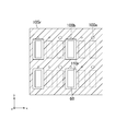
- FIG. 13 is a schematic plan view of a part of the display region 42 of the array substrate 41 of the organic EL display device 2 of the second embodiment, showing a state after the organic material layer 85 is formed.
- the formation region of the bank 84 in the display region 42, the pixel opening 60 of each of the R pixel 52r, the G pixel 52g, and the B pixel 52b, the organic material layers 85r, 85g, and 85b, and the first convex portion are illustrated.
- the positions of 100a and the second convex portion 100b are shown.
- the R pixel 52r and the G pixel 52g are arranged in the y direction, and the B pixel 52b is arranged adjacent to them in the x direction.
- the R pixel 52r and the G pixel 52g are arranged in the y direction, and the B pixel 52b is arranged adjacent to them in the x direction.
- the first convex portion 100a is provided adjacent to each B pixel 52b
- the second convex portion 100b is adjacent to each R pixel 52r and each G pixel 52g.
- the organic material layer 85b of the B pixel 52b covers only the first convex portion 100a of the two types of convex portions 100
- the organic material layer 85r of the R pixel 52r and the G pixel 52g, 85 g is provided so as not to cover either of the two types of protrusions 100a and 100b.
- the opening 110b of the B vapor deposition mask 115b includes the pixel opening 60 of the B pixel 52b on the array substrate 41 and is adjacent to the B pixel 52b, similarly to the vapor deposition mask 105b of the first embodiment.
- the protrusion 100a is formed in a shape and size.
- the openings 110r and 110g of the R and G vapor deposition masks 105r and 105g include the pixel openings 60 of the R pixel 52r and the G pixel 52g, respectively, similarly to the vapor deposition masks 105r and 105b of the first embodiment.
- the shape and size do not include any of the convex portions 100.
- the organic material layer 85 of each pixel is formed by a manufacturing method basically similar to that of the first embodiment. That is, the organic material layer 85b of the B pixel 52b is formed by supporting the vapor deposition mask 115b on the array substrate 41 using the second convex portion 100b as a spacer, and the organic material layers 85r and 85b of the R pixel 52r and the B pixel 52b are formed. Is formed by supporting the vapor deposition masks 115r and 115b on the array substrate 41 using the first convex portion 100a as a spacer.
- the deposition position accuracy is improved and the possibility of display failure is reduced. Can be planned.
- the lower one of the two types of convex portions 100 is used as a spacer of the vapor deposition mask, and the pixel on which the vapor deposition process is performed first is the preceding vapor deposition pixel, and among the plurality of types of pixels.
- a pixel that is subjected to a vapor deposition process using the higher one of the two types of convex portions 100 after the preceding vapor deposition pixel as a spacer will be referred to as a subsequent vapor deposition pixel.
- the B pixel is the preceding vapor deposition pixel
- the G pixel and the R pixel are the subsequent vapor deposition pixels.
- which one of the plurality of types of pixels is to be the preceding vapor deposition pixel is basically arbitrary from the point of the present invention, and the sequence of vapor deposition between subsequent vapor deposition pixels is basically It can be set arbitrarily.
- the vapor deposition material to the shielding region of the vapor deposition mask is increased according to the increase in the distance between the vapor deposition mask and the array substrate. Also becomes larger, and the deposition position accuracy may be lower than when the low convex portion 100 is used as a spacer. As one of measures against this, it has already been described that the opening is made small in the vapor deposition mask in which the high convex portion 100 serves as a spacer.
- the pixel openings of a plurality of types of sub-pixels having different emission colors can be set to have different sizes depending on the emission efficiency and the visibility characteristic of the emission layer of each color.
- the aperture size of the vapor deposition mask is the same, the pixel having a small pixel aperture is less affected by the displacement of the vapor deposition region than the pixel having a large pixel aperture. Therefore, among a plurality of types of pixels, one having a large pixel opening may be a preceding vapor deposition pixel, and one having a small pixel opening may be a subsequent vapor deposition pixel. As a result, even when it is difficult to further miniaturize the opening of the vapor deposition mask due to the progress of reduction of the pixel aperture, the vapor deposition position accuracy can be ensured.
- FIG. 17 shows an example of this.
- FIG. 17 is a schematic plan view of a part of the display region 42 of the array substrate 41 of the organic EL display device 2 having the stripe arrangement, similarly to the first embodiment, and the formation of the organic material layer 85. The latter state is shown.
- the pixel openings 60 of the R pixel 52r and the G pixel 52g are smaller than the B pixel 52b.
- the first convex portion 100a is arranged in the vicinity of the B pixel 52b
- the B pixel 52b is the preceding vapor deposition pixel
- the R pixel 52r and the G pixel 52g are the subsequent vapor deposition pixels. To be done.
- the first convex portion 100a does not need to be arranged adjacent to each of the preceding vapor-deposited pixels, and can be arranged at a density that suitably supports the vapor-deposition mask of the subsequent vapor-deposited pixels. Specifically, the deflection of the vapor deposition mask of the subsequent vapor deposition pixel does not occur between the protrusions 100a serving as spacers, or the protrusions 100a can be thinned to a density at which the influence of the deflection on the vapor deposition position accuracy can be ignored. ..
- the second convex portion 100b can also be thinned out.
- the arrangement density of the convex portions 100b is basically twice as high as that of the convex portions 100a, but if the intensity of the vapor deposition mask is the same for the R pixel, the G pixel, and the B pixel, the convex portion 100b has the same density.
- the density can be basically the same as that of the convex portion 100a.
- FIG. 18 is a schematic vertical sectional view of a part of the array substrate 41 having the structure, which is a sectional view taken along line Vb-Vb shown in FIG. That is, in the structure, the cross section taken along the line Va-Va shown in FIG. 4 is common to the cross section Va shown in FIG. 5, but the cross section taken along the line Vb-Vb is replaced with the cross section Vb shown in FIG. Becomes In this configuration, the second protrusion 100b shown in the cross section Vb of FIG. 5 and the like is not formed on the bank 84, and the bank 84 itself functions as the second protrusion 100b.
- the upper surface of the bank 84 supports the vapor deposition mask 105b and functions as a spacer that keeps the vapor deposition mask 105b above the pixel electrode exposed at the bottom surface of the pixel opening 60.
- the first convex portion 100a supports the vapor deposition masks 105g and 105r.
- FIG. 19 is a schematic partial plan view of the array substrate 41 of FIG. 18 after the organic material layer 85 is formed.
- the array substrate 41 of FIG. 19 is different from that of FIG. 6 in that the second convex portion 100b is not provided, but the other points are basically the same as those of FIG. 6, and especially the first convex portion 100a is Similar to FIG. 6, it is covered with the organic material layer 85b.
- the first convex portion 100a is arranged adjacent to the B pixel 52b which is the preceding vapor deposition pixel. Accordingly, the opening portion of the vapor deposition mask of the preceding vapor deposition pixel can be a single hole in which a portion provided corresponding to the pixel opening and a portion into which the first convex portion 100a is inserted can be integrated into one hole. It becomes easy to form the opening.
- the opening above the pixel opening and the opening into which the first convex portion 100a enters may be formed separately from each other.
- the present invention is not limited to the above-described embodiments and modifications, and various modifications are possible.
- the configurations described in the embodiments can be replaced with substantially the same configurations, configurations having the same operational effects, or configurations capable of achieving the same object.
Landscapes
- Engineering & Computer Science (AREA)
- Manufacturing & Machinery (AREA)
- Microelectronics & Electronic Packaging (AREA)
- Physics & Mathematics (AREA)
- General Physics & Mathematics (AREA)
- Theoretical Computer Science (AREA)
- Optics & Photonics (AREA)
- Electroluminescent Light Sources (AREA)
- Devices For Indicating Variable Information By Combining Individual Elements (AREA)
Priority Applications (3)
| Application Number | Priority Date | Filing Date | Title |
|---|---|---|---|
| CN201980074446.XA CN113170551B (zh) | 2018-11-12 | 2019-09-25 | 显示装置及其制造方法 |
| KR1020217013866A KR102615044B1 (ko) | 2018-11-12 | 2019-09-25 | 표시 장치 및 그 제조 방법 |
| US17/246,764 US11943971B2 (en) | 2018-11-12 | 2021-05-03 | OLED with one color emitting layer on a convex portion |
Applications Claiming Priority (2)
| Application Number | Priority Date | Filing Date | Title |
|---|---|---|---|
| JP2018-212367 | 2018-11-12 | ||
| JP2018212367A JP7236844B2 (ja) | 2018-11-12 | 2018-11-12 | 表示装置、及びその製造方法 |
Related Child Applications (1)
| Application Number | Title | Priority Date | Filing Date |
|---|---|---|---|
| US17/246,764 Continuation US11943971B2 (en) | 2018-11-12 | 2021-05-03 | OLED with one color emitting layer on a convex portion |
Publications (1)
| Publication Number | Publication Date |
|---|---|
| WO2020100441A1 true WO2020100441A1 (ja) | 2020-05-22 |
Family
ID=70731816
Family Applications (1)
| Application Number | Title | Priority Date | Filing Date |
|---|---|---|---|
| PCT/JP2019/037575 Ceased WO2020100441A1 (ja) | 2018-11-12 | 2019-09-25 | 表示装置、及びその製造方法 |
Country Status (5)
| Country | Link |
|---|---|
| US (1) | US11943971B2 (enExample) |
| JP (1) | JP7236844B2 (enExample) |
| KR (1) | KR102615044B1 (enExample) |
| CN (1) | CN113170551B (enExample) |
| WO (1) | WO2020100441A1 (enExample) |
Cited By (2)
| Publication number | Priority date | Publication date | Assignee | Title |
|---|---|---|---|---|
| JPWO2022224398A1 (enExample) * | 2021-04-22 | 2022-10-27 | ||
| CN115568250A (zh) * | 2022-08-30 | 2023-01-03 | 惠科股份有限公司 | 一种屏内指纹显示屏及其制造方法、显示装置 |
Families Citing this family (3)
| Publication number | Priority date | Publication date | Assignee | Title |
|---|---|---|---|---|
| WO2020158566A1 (ja) * | 2019-01-31 | 2020-08-06 | 大日本印刷株式会社 | 蒸着マスク群、電子デバイスの製造方法及び電子デバイス |
| CN113555397B (zh) * | 2021-07-08 | 2023-03-24 | 武汉华星光电半导体显示技术有限公司 | 显示面板 |
| JP7767139B2 (ja) * | 2021-12-24 | 2025-11-11 | 株式会社Magnolia White | 表示装置 |
Citations (7)
| Publication number | Priority date | Publication date | Assignee | Title |
|---|---|---|---|---|
| JP2006086504A (ja) * | 2004-09-16 | 2006-03-30 | Lg Phillips Lcd Co Ltd | 有機電界発光素子及びその製造方法 |
| JP2011100553A (ja) * | 2009-11-04 | 2011-05-19 | Seiko Epson Corp | 有機el装置、有機el装置の製造方法、電子機器 |
| JP2011170981A (ja) * | 2010-02-16 | 2011-09-01 | Toppan Printing Co Ltd | 有機エレクトロルミネッセンス素子及びその製造方法 |
| JP2011181305A (ja) * | 2010-03-01 | 2011-09-15 | Toppan Printing Co Ltd | 有機エレクトロルミネッセンス素子及びその製造方法 |
| JP2013089475A (ja) * | 2011-10-19 | 2013-05-13 | Canon Inc | 発光表示装置及びその製造方法 |
| JP2014212070A (ja) * | 2013-04-19 | 2014-11-13 | ソニー株式会社 | 表示装置およびその製造方法、ならびに電子機器 |
| JP2015149309A (ja) * | 2004-09-29 | 2015-08-20 | 株式会社半導体エネルギー研究所 | 表示装置 |
Family Cites Families (16)
| Publication number | Priority date | Publication date | Assignee | Title |
|---|---|---|---|---|
| JP2001089841A (ja) * | 1999-09-22 | 2001-04-03 | Sony Corp | 表面加工用冶具及び表面加工方法 |
| JP4053209B2 (ja) | 2000-05-01 | 2008-02-27 | 三星エスディアイ株式会社 | 有機elディスプレイの製造方法 |
| JP3481232B2 (ja) | 2002-03-05 | 2003-12-22 | 三洋電機株式会社 | 有機エレクトロルミネッセンスパネルの製造方法 |
| JP2005322564A (ja) * | 2004-05-11 | 2005-11-17 | Sony Corp | 表示装置の製造方法および表示装置 |
| TWI460851B (zh) * | 2005-10-17 | 2014-11-11 | Semiconductor Energy Lab | 半導體裝置及其製造方法 |
| JP2009272277A (ja) * | 2008-05-12 | 2009-11-19 | Seiko Epson Corp | 有機エレクトロルミネッセンス素子、有機エレクトロルミネッセンス素子の製造方法、有機エレクトロルミネッセンス装置、有機エレクトロルミネッセンス装置の製造方法 |
| KR101571513B1 (ko) * | 2009-07-21 | 2015-11-25 | 삼성디스플레이 주식회사 | 유기 발광 표시 장치 및 그 제조 방법 |
| KR101997122B1 (ko) * | 2012-07-27 | 2019-07-08 | 삼성디스플레이 주식회사 | 유기 발광 표시 장치 및 이의 제조 방법 |
| KR20150005264A (ko) * | 2013-07-05 | 2015-01-14 | 삼성디스플레이 주식회사 | 유기 발광 표시 장치 및 그 제조 방법 |
| KR101683742B1 (ko) * | 2014-04-25 | 2016-12-08 | 삼성디스플레이 주식회사 | 유기 발광 표시 장치 |
| JP2016018734A (ja) * | 2014-07-10 | 2016-02-01 | 株式会社ジャパンディスプレイ | 表示装置及びその製造方法 |
| KR102442616B1 (ko) * | 2015-04-08 | 2022-09-14 | 삼성디스플레이 주식회사 | 유기 발광 표시 장치 및 그 제조 방법 |
| KR102467213B1 (ko) * | 2015-07-28 | 2022-11-15 | 엘지디스플레이 주식회사 | 유기발광다이오드 표시장치 |
| KR102604310B1 (ko) * | 2016-12-30 | 2023-11-20 | 엘지디스플레이 주식회사 | 유기 발광 표시 장치 |
| KR20200076278A (ko) * | 2018-12-19 | 2020-06-29 | 엘지디스플레이 주식회사 | 유기 발광 표시 장치 |
| CN110048005B (zh) * | 2019-03-29 | 2020-06-16 | 武汉华星光电半导体显示技术有限公司 | 一种oled显示器件及其制备方法 |
-
2018
- 2018-11-12 JP JP2018212367A patent/JP7236844B2/ja active Active
-
2019
- 2019-09-25 WO PCT/JP2019/037575 patent/WO2020100441A1/ja not_active Ceased
- 2019-09-25 KR KR1020217013866A patent/KR102615044B1/ko active Active
- 2019-09-25 CN CN201980074446.XA patent/CN113170551B/zh active Active
-
2021
- 2021-05-03 US US17/246,764 patent/US11943971B2/en active Active
Patent Citations (7)
| Publication number | Priority date | Publication date | Assignee | Title |
|---|---|---|---|---|
| JP2006086504A (ja) * | 2004-09-16 | 2006-03-30 | Lg Phillips Lcd Co Ltd | 有機電界発光素子及びその製造方法 |
| JP2015149309A (ja) * | 2004-09-29 | 2015-08-20 | 株式会社半導体エネルギー研究所 | 表示装置 |
| JP2011100553A (ja) * | 2009-11-04 | 2011-05-19 | Seiko Epson Corp | 有機el装置、有機el装置の製造方法、電子機器 |
| JP2011170981A (ja) * | 2010-02-16 | 2011-09-01 | Toppan Printing Co Ltd | 有機エレクトロルミネッセンス素子及びその製造方法 |
| JP2011181305A (ja) * | 2010-03-01 | 2011-09-15 | Toppan Printing Co Ltd | 有機エレクトロルミネッセンス素子及びその製造方法 |
| JP2013089475A (ja) * | 2011-10-19 | 2013-05-13 | Canon Inc | 発光表示装置及びその製造方法 |
| JP2014212070A (ja) * | 2013-04-19 | 2014-11-13 | ソニー株式会社 | 表示装置およびその製造方法、ならびに電子機器 |
Cited By (3)
| Publication number | Priority date | Publication date | Assignee | Title |
|---|---|---|---|---|
| JPWO2022224398A1 (enExample) * | 2021-04-22 | 2022-10-27 | ||
| JP7515013B2 (ja) | 2021-04-22 | 2024-07-11 | シャープディスプレイテクノロジー株式会社 | 表示装置及び表示装置の製造方法 |
| CN115568250A (zh) * | 2022-08-30 | 2023-01-03 | 惠科股份有限公司 | 一种屏内指纹显示屏及其制造方法、显示装置 |
Also Published As
| Publication number | Publication date |
|---|---|
| US11943971B2 (en) | 2024-03-26 |
| JP7236844B2 (ja) | 2023-03-10 |
| JP2020080224A (ja) | 2020-05-28 |
| KR20210060622A (ko) | 2021-05-26 |
| CN113170551A (zh) | 2021-07-23 |
| KR102615044B1 (ko) | 2023-12-19 |
| US20210257423A1 (en) | 2021-08-19 |
| CN113170551B (zh) | 2024-11-05 |
Similar Documents
| Publication | Publication Date | Title |
|---|---|---|
| US11296172B2 (en) | Semiconductor device | |
| US11943971B2 (en) | OLED with one color emitting layer on a convex portion | |
| KR20230044996A (ko) | 유기 발광 표시 패널 | |
| KR102510569B1 (ko) | 유기 발광 표시 장치 | |
| US10756310B2 (en) | Display device | |
| TW201413939A (zh) | 有機發光二極體顯示器 | |
| JP2015195094A (ja) | 有機el表示装置 | |
| KR20170113866A (ko) | 디스플레이장치 | |
| US12317694B2 (en) | Display device | |
| WO2019026131A1 (ja) | 表示デバイス | |
| KR20040015935A (ko) | 듀얼패널타입 유기전계발광 소자 및 그의 제조방법 | |
| WO2020065992A1 (ja) | 表示デバイス | |
| JP4639662B2 (ja) | 電気光学装置および電子機器 | |
| WO2022244160A1 (ja) | 表示装置 | |
| KR20220043544A (ko) | 발광 표시 장치 | |
| KR101274699B1 (ko) | 유기 발광 소자 | |
| US10978521B2 (en) | Display device | |
| WO2019064564A1 (ja) | 表示デバイス | |
| US20230380248A1 (en) | Display device | |
| WO2020065794A1 (ja) | 表示装置 | |
| JP7220084B2 (ja) | 表示装置 | |
| KR20240106365A (ko) | 유기발광다이오드 표시장치 | |
| CN120787062A (zh) | 显示面板及电子设备 |
Legal Events
| Date | Code | Title | Description |
|---|---|---|---|
| 121 | Ep: the epo has been informed by wipo that ep was designated in this application |
Ref document number: 19884788 Country of ref document: EP Kind code of ref document: A1 |
|
| ENP | Entry into the national phase |
Ref document number: 20217013866 Country of ref document: KR Kind code of ref document: A |
|
| NENP | Non-entry into the national phase |
Ref country code: DE |
|
| 122 | Ep: pct application non-entry in european phase |
Ref document number: 19884788 Country of ref document: EP Kind code of ref document: A1 |