WO2020100357A1 - プラズマ処理装置 - Google Patents
プラズマ処理装置 Download PDFInfo
- Publication number
- WO2020100357A1 WO2020100357A1 PCT/JP2019/030660 JP2019030660W WO2020100357A1 WO 2020100357 A1 WO2020100357 A1 WO 2020100357A1 JP 2019030660 W JP2019030660 W JP 2019030660W WO 2020100357 A1 WO2020100357 A1 WO 2020100357A1
- Authority
- WO
- WIPO (PCT)
- Prior art keywords
- plasma processing
- processing apparatus
- power supply
- voltage
- waveform
- Prior art date
- Legal status (The legal status is an assumption and is not a legal conclusion. Google has not performed a legal analysis and makes no representation as to the accuracy of the status listed.)
- Ceased
Links
Images








Classifications
-
- H—ELECTRICITY
- H01—ELECTRIC ELEMENTS
- H01J—ELECTRIC DISCHARGE TUBES OR DISCHARGE LAMPS
- H01J37/00—Discharge tubes with provision for introducing objects or material to be exposed to the discharge, e.g. for the purpose of examination or processing thereof
- H01J37/32—Gas-filled discharge tubes
- H01J37/32431—Constructional details of the reactor
- H01J37/32532—Electrodes
- H01J37/32577—Electrical connecting means
-
- H—ELECTRICITY
- H01—ELECTRIC ELEMENTS
- H01J—ELECTRIC DISCHARGE TUBES OR DISCHARGE LAMPS
- H01J37/00—Discharge tubes with provision for introducing objects or material to be exposed to the discharge, e.g. for the purpose of examination or processing thereof
- H01J37/32—Gas-filled discharge tubes
- H01J37/32009—Arrangements for generation of plasma specially adapted for examination or treatment of objects, e.g. plasma sources
- H01J37/32082—Radio frequency generated discharge
- H01J37/32137—Radio frequency generated discharge controlling of the discharge by modulation of energy
- H01J37/32146—Amplitude modulation, includes pulsing
-
- H—ELECTRICITY
- H01—ELECTRIC ELEMENTS
- H01J—ELECTRIC DISCHARGE TUBES OR DISCHARGE LAMPS
- H01J37/00—Discharge tubes with provision for introducing objects or material to be exposed to the discharge, e.g. for the purpose of examination or processing thereof
- H01J37/32—Gas-filled discharge tubes
- H01J37/32009—Arrangements for generation of plasma specially adapted for examination or treatment of objects, e.g. plasma sources
- H01J37/32082—Radio frequency generated discharge
- H01J37/32128—Radio frequency generated discharge using particular waveforms, e.g. polarised waves
-
- H—ELECTRICITY
- H01—ELECTRIC ELEMENTS
- H01J—ELECTRIC DISCHARGE TUBES OR DISCHARGE LAMPS
- H01J37/00—Discharge tubes with provision for introducing objects or material to be exposed to the discharge, e.g. for the purpose of examination or processing thereof
- H01J37/32—Gas-filled discharge tubes
- H01J37/32009—Arrangements for generation of plasma specially adapted for examination or treatment of objects, e.g. plasma sources
- H01J37/32082—Radio frequency generated discharge
- H01J37/32174—Circuits specially adapted for controlling the RF discharge
-
- H—ELECTRICITY
- H01—ELECTRIC ELEMENTS
- H01J—ELECTRIC DISCHARGE TUBES OR DISCHARGE LAMPS
- H01J37/00—Discharge tubes with provision for introducing objects or material to be exposed to the discharge, e.g. for the purpose of examination or processing thereof
- H01J37/32—Gas-filled discharge tubes
- H01J37/32009—Arrangements for generation of plasma specially adapted for examination or treatment of objects, e.g. plasma sources
- H01J37/32082—Radio frequency generated discharge
- H01J37/32174—Circuits specially adapted for controlling the RF discharge
- H01J37/32183—Matching circuits
-
- H—ELECTRICITY
- H01—ELECTRIC ELEMENTS
- H01J—ELECTRIC DISCHARGE TUBES OR DISCHARGE LAMPS
- H01J37/00—Discharge tubes with provision for introducing objects or material to be exposed to the discharge, e.g. for the purpose of examination or processing thereof
- H01J37/32—Gas-filled discharge tubes
- H01J37/32431—Constructional details of the reactor
- H01J37/32715—Workpiece holder
-
- H—ELECTRICITY
- H05—ELECTRIC TECHNIQUES NOT OTHERWISE PROVIDED FOR
- H05H—PLASMA TECHNIQUE; PRODUCTION OF ACCELERATED ELECTRICALLY-CHARGED PARTICLES OR OF NEUTRONS; PRODUCTION OR ACCELERATION OF NEUTRAL MOLECULAR OR ATOMIC BEAMS
- H05H1/00—Generating plasma; Handling plasma
- H05H1/24—Generating plasma
- H05H1/46—Generating plasma using applied electromagnetic fields, e.g. high frequency or microwave energy
-
- H—ELECTRICITY
- H10—SEMICONDUCTOR DEVICES; ELECTRIC SOLID-STATE DEVICES NOT OTHERWISE PROVIDED FOR
- H10P—GENERIC PROCESSES OR APPARATUS FOR THE MANUFACTURE OR TREATMENT OF DEVICES COVERED BY CLASS H10
- H10P50/00—Etching of wafers, substrates or parts of devices
- H10P50/20—Dry etching; Plasma etching; Reactive-ion etching
- H10P50/24—Dry etching; Plasma etching; Reactive-ion etching of semiconductor materials
- H10P50/242—Dry etching; Plasma etching; Reactive-ion etching of semiconductor materials of Group IV materials
-
- H—ELECTRICITY
- H10—SEMICONDUCTOR DEVICES; ELECTRIC SOLID-STATE DEVICES NOT OTHERWISE PROVIDED FOR
- H10P—GENERIC PROCESSES OR APPARATUS FOR THE MANUFACTURE OR TREATMENT OF DEVICES COVERED BY CLASS H10
- H10P72/00—Handling or holding of wafers, substrates or devices during manufacture or treatment thereof
- H10P72/70—Handling or holding of wafers, substrates or devices during manufacture or treatment thereof for supporting or gripping
-
- H—ELECTRICITY
- H01—ELECTRIC ELEMENTS
- H01J—ELECTRIC DISCHARGE TUBES OR DISCHARGE LAMPS
- H01J2237/00—Discharge tubes exposing object to beam, e.g. for analysis treatment, etching, imaging
- H01J2237/32—Processing objects by plasma generation
- H01J2237/33—Processing objects by plasma generation characterised by the type of processing
- H01J2237/334—Etching
Definitions
- the present invention relates to a plasma processing device.
- lithography technology is used to mold fine patterns in the manufacturing process of semiconductor devices. This technique applies a device structure pattern on a resist layer and selectively etches away the substrate exposed by the resist layer pattern. In subsequent processing steps, other materials may be deposited in the etched areas to form integrated circuits.
- plasma etching processing equipment is indispensable for manufacturing semiconductor devices.
- the gas supplied to the inside of the processing chamber which has been depressurized to a predetermined vacuum degree, is turned into plasma by an electric field or the like formed inside the vacuum container.
- highly reactive ions and radicals generated in the plasma physically and chemically react with the surface of the wafer to be processed, thereby performing etching.
- etching processing it is widely practiced to apply a high frequency voltage to the wafer mounting table.
- a high-frequency voltage is applied to the mounting table to which a high-frequency power source is connected via a capacitor
- the mounting table becomes a negative voltage on time average due to self-bias. Therefore, positive ions are accelerated, etching progresses rapidly, and verticality increases, so that anisotropic etching can be realized.
- the etching rate and verticality can be controlled by adjusting the amplitude of the high-frequency voltage applied to the mounting table.
- a sine wave is used as the high frequency voltage applied to the wafer mounting table, but as disclosed in Patent Document 1, a rectangular wave may be used instead of the sine wave.
- the energy of the ions flowing from the plasma to the mounting table is determined by the electric field applied between the plasma and the mounting table.
- the electric field changes gently, so that ions of various energies flow into the mounting table.
- the ion energy is clearly divided into high energy and low energy, which facilitates the control of etching.
- the dielectric material formed on the wafer is charged by the collision of charged particles.
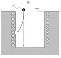
- a trench shape is often formed on the wafer as shown in FIG. 1, and in this case, it is generally desirable that the sidewall of the trench be perpendicular to the wafer surface. ..
- the sidewall of the trench may be charged as shown in FIG. This is because positive ions are vertically injected into the trench due to the negative self-bias due to the high frequency voltage, whereas the directions of electrons and negative ions are random, so that more negatively charged particles collide with the side walls. Because it does.
- the ions (Ion) flying in the trench are bent and collide with the side wall, and the side wall is etched, so that the verticality of the side wall of the trench is deteriorated. Invite.
- a metal layer that should not be etched in a part of the trench.
- the ions are obliquely incident on the metal layer.
- the metal layer is more likely to be sputtered than when the ions are vertically incident, so that the metal layer is damaged more and the desired etching may not be performed. From the above, removing charged particles charged on the wafer surface is a problem in performing highly accurate etching processing.
- Patent Document 1 In order to remove the charged particles on the surface of the wafer, a voltage having a polarity opposite to that of the charged particles is applied to the wafer to form an electric field inside the dielectric material formed on the wafer, so that the continuous operation of the charged particles is continued. Generating an electric current is one measure. However, it is known that it takes a time of the order of milliseconds to remove the charged particles from the dielectric material because the moving speed of the charged particles inside the dielectric material is low.
- the high frequency voltage as disclosed in Patent Document 1 is generally used at a frequency of several hundred kHz to several MHz so that it can pass through a capacitor between the mounting table and the high frequency power source. Therefore, the technique of Patent Document 1 is not suitable for removing charged particles.
- the present invention provides a plasma processing apparatus capable of obtaining a trench shape having high verticality by removing charged particles on the surface of a wafer and reducing damage to a film which is not an etching target inside the trench.
- the purpose is to
- one of the typical plasma processing apparatuses is a processing chamber in which a sample is plasma-processed, and a first high-frequency power supply that supplies high-frequency power for generating plasma.
- a plasma processing apparatus including a sample stage on which the sample is placed and a second high-frequency power source that supplies high-frequency power to the sample stage, a DC voltage changed by a periodically repeated waveform is applied to the sample stage. This is achieved by further comprising a DC power supply for applying to the above, and the one cycle of the waveform has a period of an amplitude that changes by a predetermined amount or more in a predetermined time.
- a highly vertical trench shape can be obtained, and a plasma processing apparatus capable of reducing damage to a film that is not an etching target inside the trench. Can be provided. Problems, configurations, and effects other than those described above will be clarified by the following description of the embodiments.
- FIG. 1 is a schematic diagram showing a trench shape in a plasma etching process and an ion trajectory when a side wall thereof is charged.
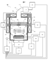
- FIG. 2 is a schematic diagram showing an example of a schematic configuration of the plasma processing apparatus according to the present embodiment.
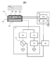
- FIG. 3 is a cross-sectional view of a part of the plasma processing apparatus according to the embodiment shown in FIG. 1 and a diagram schematically showing an outline of a bias voltage generating unit connected to the mounting table.
- FIG. 4 is a diagram showing an electrical equivalent circuit of the plasma processing apparatus.
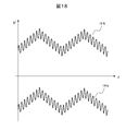
- FIG. 5 is a diagram showing voltage waveforms output from the DC power supply according to the embodiment shown in FIG. 6 is a diagram showing a waveform of a current calculated by a circuit simulator based on the equivalent circuit of FIG.
- FIG. 4 is a diagram schematically showing a current generated on the wafer by the voltage of FIG.
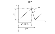
- FIG. 7 is a diagram showing a voltage waveform of a modified linear triangular wave.
- FIG. 8 is a diagram showing a voltage waveform applied to a curved triangular wave.
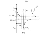
- FIG. 9 is a diagram showing the waveform of the current flowing from the wafer.
- FIG. 10 is a diagram showing the relationship between the output start and end times of the microwave power supply, the high frequency power supply, and the DC power supply.
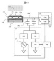
- FIG. 11 is a cross-sectional view of a part of the plasma processing apparatus according to the first modification of the embodiment shown in FIG. 1 and a diagram schematically showing an outline of the bias voltage generating unit connected to the mounting table.
- FIG. 11 is a cross-sectional view of a part of the plasma processing apparatus according to the first modification of the embodiment shown in FIG. 1 and a diagram schematically showing an outline of the bias voltage generating unit connected to the mounting table.
- FIG. 12 is a cross-sectional view of a part of the plasma processing apparatus according to the modified example 2 of the embodiment shown in FIG. 1 and a diagram schematically showing the outline of the bias voltage generator connected to the mounting table.
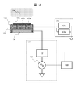
- FIG. 13 is a cross-sectional view of a part of the plasma processing apparatus according to the modified example 3 of the embodiment shown in FIG. 1 and a diagram schematically showing the outline of the bias voltage generating unit connected to the mounting table.
- FIG. 14 is a diagram showing a voltage waveform output from the electrostatic attraction power supply in the third modification of the embodiment shown in FIG.
- FIG. 15 is a cross-sectional view of a part of the plasma processing apparatus according to the modified example 4 of the embodiment shown in FIG.
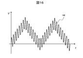
- FIG. 16 is a diagram showing a voltage waveform output from the bias voltage generator in the modification 4 of the embodiment shown in FIG.
- FIG. 17 is a cross-sectional view of a part of the plasma processing apparatus according to the modified example 5 of the embodiment shown in FIG. 1 and a diagram schematically showing the outline of the bias voltage generation unit connected to the mounting table.
- FIG. 18 is a diagram showing a voltage waveform output from the electrostatic attraction power supply in the modified example 5 of the embodiment shown in FIG. 1.
- linear triangular wave of the voltage waveform means that the voltage linearly rises from the minimum voltage to the maximum voltage, and immediately after reaching the maximum voltage, linearly decreases to the minimum voltage.
- a “curve triangular wave” of a voltage waveform refers to a voltage curve “triangular wave” that rises from the minimum voltage to the maximum voltage along a curve in which the positive differential coefficient monotonically decreases, and immediately after reaching the maximum voltage, the negative differential to the minimum voltage. This is a waveform in which the coefficient periodically decreases along a curve that monotonically increases.
- FIG. 2 is a schematic diagram showing an example of a schematic configuration of the plasma processing apparatus according to the present embodiment.
- the plasma processing apparatus 100 is an example of a microwave ECR plasma etching apparatus.
- the electrodes arranged inside the vacuum processing chamber 104, the electric field and magnetic field generators arranged outside the vacuum processing chamber 104, the power supply, and the like are schematically shown.
- the plasma processing apparatus 100 includes a vacuum processing chamber 104.
- An electrode 125 which is a sample stand is arranged inside the vacuum processing chamber 104, and a wafer 126 which is a sample is placed on the electrode 125.
- the electric field and the magnetic field formed by the electric field generating means and the magnetic field generating means arranged outside the vacuum processing chamber 104 act on the gas supplied from the gas supply mechanism 105 to the vacuum processing chamber 104. By doing so, plasma 136 is generated.
- the plasma 136 contains ions and radicals, which interact with the surface of the wafer 126 to perform a plasma etching process.
- a shower plate 102 is arranged above the container 101, and a dielectric window 103 is arranged further above, and the container 101 surrounding the vacuum processing chamber 104 is hermetically sealed by the dielectric window 103. ..
- a gas supply mechanism 105 provided outside the vacuum processing chamber 104 is connected to a space 107 provided between the dielectric window 103 and the shower plate 102 through a gas pipe 106.
- the space 107 communicates with the vacuum processing chamber 104 through a plurality of pores 108 provided in the shower plate 102.
- a variable conductance valve 112 is arranged below the vacuum processing chamber 104, and a gas in the vacuum processing chamber 104 is exhausted by a turbo molecular pump 113 connected through the variable conductance valve 112.
- the turbo molecular pump 113 is further connected to the roughing pump 114.
- the variable conductance valve 112, the turbo molecular pump 113, and the roughing pump 114 are connected to the control unit 150, and their operations are controlled by the control unit 150.
- a pressure gauge 115 for measuring the internal pressure of the vacuum processing chamber 104 is provided, and the control unit 150 feedback-controls the opening degree of the variable conductance valve 112 according to the value of the pressure gauge 115.
- the pressure in the vacuum processing chamber 104 is controlled to a desired value.
- a microwave power supply 116 that is a first high-frequency power supply is provided above the plasma processing apparatus 100, and the frequency of the microwave power supply 116 is, for example, 2.45 GHz.
- the microwave generated from the microwave power source 116 propagates to the cavity resonator 121 through the automatic matching device 117, the rectangular waveguide 118, the rectangular circular waveguide converter 119, and the circular waveguide 120.
- the automatic matching device 117 has a function of automatically suppressing reflected waves
- the cavity resonator 121 has a function of adjusting the microwave electromagnetic field distribution to a distribution suitable for plasma processing.
- the microwave power supply 116 is controlled by the control unit 150.
- a vacuum processing chamber 104 is provided below the cavity resonator 121 with the dielectric window 103, which is a microwave introduction window, and the shower plate 102 interposed therebetween.
- the microwave whose distribution has been adjusted by the cavity resonator 121 propagates to the vacuum processing chamber 104 via the dielectric window 103 and the shower plate 102.
- solenoid coils 122, 123, and 124 forming an electromagnet are arranged.
- a magnetic field is formed inside the vacuum processing chamber 104 by causing a current to flow through the solenoid coils 122, 123, and 124 by the coil power supply 140 controlled by the control unit 150.
- the region where the electric field and the magnetic field strength have a specific relationship for example, when the electric field is 2.45 GHz, the magnetic field strength is 0.
- plasma is formed by electron cyclotron resonance (ECR) described later.
- the ECR is explained in detail below.
- the electrons existing inside the vacuum processing chamber 104 move while rotating along the lines of magnetic force of the magnetic field generated by the solenoid coils 122, 123, and 124 due to the Lorentz force.
- the frequency of the microwave propagated from the microwave power source 116 matches the frequency of the rotation, the electrons are resonantly accelerated and plasma is effectively generated. This is called ECR.
- the area (ECR surface) where ECR occurs can be controlled by the magnetic field distribution.
- the control unit 150 controls the magnetic field distribution inside the vacuum processing chamber 104 by controlling the current flowing through each of the solenoid coils 122, 123, and 124 via the coil power supply 140, and the inside of the vacuum processing chamber 104 is controlled.
- the plasma generation area can be controlled. Further, since the diffusion of charged particles in the plasma is suppressed in the direction perpendicular to the lines of magnetic force, it is possible to control the diffusion of the plasma by controlling the magnetic field distribution and reduce the plasma loss. Due to these effects, the distribution of plasma above the wafer 126 can be controlled and the uniformity of plasma processing can be improved.
- the electrode 125 is located below the ECR surface and is fixed to the vacuum processing chamber 104 by a beam (not shown).
- the electrode 125 and the vacuum processing chamber 104 have a substantially cylindrical shape, and the central axes of the respective cylinders are the same.
- the plasma processing apparatus 100 is provided with a transfer device (not shown) such as a robot arm, and the wafer 126, which is a processing target, is transferred to the upper part of the electrode 125 by the transfer device.
- the wafer 126 is held on the electrode 125 by electrostatic attraction of the electrostatic attraction electrode 135 formed inside the electrode 125.
- a bias voltage generator 127 is connected to the electrode 125, and a bias voltage is applied to the wafer 126 through the bias voltage generator 127.
- the amount of ions in the plasma 136 that are drawn to the side of the wafer 126 depends on the bias voltage. Therefore, by controlling the bias voltage generator 127 by the controller 150 to adjust the bias voltage generated on the wafer 126, the plasma processing shape (etching shape distribution) can be controlled.
- a temperature control mechanism 128 is mounted on the electrode 125, and the plasma processing shape can be controlled by controlling the temperature of the wafer 126 through the electrode 125.
- control computer that is the control unit 150
- timing and operation amount are controlled so that they operate in an appropriate sequence.
- Detailed parameters of the operation sequence are called recipes, and control is performed based on preset recipes.
- Recipes usually consist of multiple steps.
- Processing conditions such as a voltage mode are set, and each step is executed in a preset order and time.
- FIG. 3 is a schematic diagram showing the cross section of the electrode 125 and the details of the bias voltage generator 127 according to the embodiment shown in FIG.
- the electrode 125 has a conductor base material 129 and a dielectric film 130, and the bias voltage generating section 127 is connected to the base material 129. Further, the electrode 125 has electrostatic attraction electrodes 135a and 135b between the wafer 126 and the base material 129, respectively, and the electrostatic attraction electrodes 135a and 135b are insulated from the surroundings by the dielectric film 130.
- the electrostatic adsorption electrode 135a is annularly arranged on the outer periphery of the electrode, and the electrostatic adsorption electrode 135b is arranged inside the electrostatic adsorption electrode 135a and in the central portion of the electrode.
- the electrostatic attraction power supply 139 has power supply units 139a and 139b, the power supply unit 139a is connected to the electrostatic attraction electrode 135a, and the power supply unit 139b is connected to the electrostatic attraction electrode 135b.
- the bias voltage generating unit 127 includes a high frequency power supply (second high frequency power supply) 131, an automatic matching device 132, a DC power supply 133 that outputs a DC voltage changed by a cyclically repeated waveform, and a low pass filter 134.
- the power supply 131 is connected to the base material 129 via the automatic matching device 132, and the DC power supply 133 is connected to the base material 129 via the low-pass filter 134.
- the high frequency power supply 131 and the direct current power supply 133 are connected to the control unit (control mechanism) 150, respectively, and their operations are controlled according to signals from the control unit 150.
- the output frequency of the high frequency power supply 131 is lower than that of the microwave power supply 116 and high enough to transmit the bias voltage to the wafer 126 via the dielectric film 130. Specifically, several hundred kHz to several MHz are used as the output frequency of the high frequency power supply 131.
- the automatic matching unit 132 performs impedance matching by changing the circuit constant of the internal element according to the impedance of the plasma 136, so that the high frequency power supply 131 can efficiently transfer the power to the wafer 126.
- FIG. 4 shows an electrical equivalent circuit of the plasma processing apparatus 100.
- the output from the bias voltage generator 127 passes through a point 129 ′ corresponding to the base material 129, a capacitor 130 ′ corresponding to the dielectric film 130, a point 126 ′ corresponding to the wafer 126, and between the wafer 126 and the plasma 136. 1 is transmitted to the ground 137 'through the parallel circuit 138a corresponding to the sheath of the plasma, the resistor 136' corresponding to the plasma 136, and the parallel circuit 138b corresponding to the sheath between the plasma 136 and the ground 137 'corresponding to the ground 137 of FIG. To be done.
- the relationship of I A ⁇ dV / dt is generally established between the voltage V generated by the bias voltage generator 127 and the current I flowing from the wafer 126 using the proportional constant A.
- FIG. 5 is a diagram showing a voltage waveform output from the DC power supply 133.
- the DC power supply 133 outputs a voltage that changes according to a linear triangular wave 151 having a frequency f t and an amplitude V t according to a command from the control unit 150. That is, the voltage waveform output from the DC power supply 133 has a period in which the waveform of one cycle has an amplitude that changes by a predetermined amount or more in a predetermined time. Since the current I flowing from the wafer is proportional to the differential of the voltage of the bias voltage generator 127, a rectangular wave-shaped current, which is the differential of the linear triangular wave, flows from the wafer.
- the continuation of the current I flowing from the wafer which is proportional to the differential value of the voltage, is instantaneously terminated.
- the current I continues to flow while the voltage rises or falls.
- the duration of the current I is at least 1 ms or longer, and the longer the current, the better. Therefore, the use of the linear triangular wave enhances the effect of removing charges from the wafer surface, rather than the rectangular wave in which the duration of the current I is short. The same effect can be obtained for the curved triangular wave described later.
- the curved triangular wave reduces damage to the metal layer that is not the target of etching.
- the duration of the current I of is important.
- f t In order to move the charged particles accumulated inside the dielectric on the wafer to the outside of the dielectric, time on the order of milliseconds is required. If positive or negative current flowing from the wafer lasts less than 1 ms each, the dielectric Only charged particles are attracted inside the body and then returned. Therefore, f t needs to be approximately 500 Hz or less. If this condition is satisfied, the positive and negative currents continue for 1 ms or more, respectively, so that the charged particles are effectively removed.
- the mobility within the wafer may differ between positive and negative charges.
- a voltage that changes according to the modified linear triangular wave 153 as shown in FIG. 7 is output from the DC power supply 133 so that as much current as possible flows from the wafer while surely removing both charges regardless of the mobility. Good.
- the ratio of the time for the voltage to rise from the minimum value to the maximum value and the time for the voltage to fall from the maximum value to the minimum value is D t : (1-D t ).
- D t is a value obtained by dividing the ion mobility by the sum of the electron mobility in the dielectric on the wafer and the ion mobility in the dielectric.
- the frequency f p in order to secure the time of each polarity for 1 ms or more, the frequency f p must be determined so as to satisfy both f p ⁇ 1000D t and f p ⁇ 1000 (1-D t ).
- the unit of f p is Hz.
- the frequency f p of the triangular waveform is preferably a value obtained by subtracting D t from 1 or a value obtained by multiplying the smaller value of D t by 1000 times in Hz.
- the linear triangular wave output from the DC power supply is superimposed in addition to the high frequency bias voltage applied to the mounting table, so that a current that lasts for a sufficient time to remove the charged particles on the wafer surface is generated. To do. This current removes the charged particles on the surface of the sample, so that a highly vertical trench shape can be obtained, and damage to the film inside the trench which is not the etching target can be reduced.
- the curved triangular wave 154 can be regarded as a rectangular wave having a large time constant, but it has characteristics similar to the linear triangular wave.
- the rising time constant ⁇ r and the falling time constant ⁇ f are each 0.43 ms or more, typically about several ms. Is desirable.
- the frequency f p of the curved triangular wave 154 must be 500 Hz or less.
- the current 155 flowing from the wafer maintains 10% or more of the maximum value and continues for 1 ms or more from the start of the voltage rise and fall, so that the charged particles can be removed. Can contribute.
- the change time and the change amount of the amplitude of the voltage waveform output from the DC power supply are the change time and the change amount of the amplitude for maintaining 10% or more of the maximum value of the current generated on the wafer by the voltage waveform for 1 ms or more. And preferred.
- the duty ratio D p of the curved triangular wave 154 may be set to a value other than 50% in consideration of the difference in mobility ⁇ e and ⁇ i of electrons and ions inside the on-wafer dielectric.
- D p is a value obtained by dividing the ion mobility by the sum of the electron mobility in the dielectric on the wafer and the ion mobility in the dielectric.
- the frequency f p in order to secure each polarity time of 1 ms or more, the frequency f p must be determined so as to satisfy both f p ⁇ 1000D t and f p ⁇ 1000 (1 ⁇ D t ).
- the unit of f p is Hz.
- the frequency fp of the triangular waveform is preferably a value obtained by subtracting D p from 1 or a value obtained by multiplying the smaller value of D p by 1000 times in units of Hz.
- the control of the DC power supply 133 becomes easy as in the case of using the rectangular wave.
- the control signal output from the control unit 150 may alternately output two states of ON and OFF, and the time constants ⁇ r and ⁇ f are the control signal or the output of the DC power supply 133.
- a low-pass filter may be applied, or output feedback may be provided to the DC power supply 133.
- the waveforms 151, 153, and 154 are shown such that the voltage is always positive, but in reality, the waveform is such that the voltage is always negative or crosses between positive and negative. May be This is because the current flowing from the wafer is the differential of the voltage, and the positive / negative of the voltage has no effect.
- FIG. 10 is a diagram showing the relationship between the output start and end times of (a) high frequency power supply 131, (b) microwave power supply 116, and (c) direct current power supply 133, with the vertical axis indicating output and the horizontal axis indicating time. Is shown. It is desirable that the output of the microwave power supply 116 be started before the output of the high frequency power supply 131 is started. This is because the impedance of the chamber when viewed from the high frequency power supply 131 differs greatly depending on the presence or absence of plasma. Therefore, starting the output of the high frequency power supply 131 after the plasma is generated by the output of the microwave power supply 116 is the output of the high frequency power supply 131. Is stable. For the same reason, it is desirable that the output of the high frequency power supply 131 be completed before the output of the microwave power supply 116 is completed.
- the output of the DC power supply 133 be started before the output of the high frequency power supply 131 is started. This is for the following reason.
- the voltage between the plasma 136 and the wafer 126 becomes high, so that the verticality of the charged particles drawn into the wafer 126 becomes high, and the trench sidewall on the wafer 126 is charged. Easier to do.
- the output of the DC power supply 133 does not adversely affect the device and the etching result. Therefore, by setting the output of the DC power supply 133 before the output of the high frequency power supply 131, it becomes possible to more effectively suppress the charging of the sidewall of the trench. For the same reason, it is desirable that the output of the DC power supply 133 be completed after the output of the high frequency power supply 131 is completed.
- the relationship between the output timings of the DC power supply 133 and the microwave power supply 116 be the same as the relationship between the output timings of the DC power supply 133 and the high frequency power supply 131 described above. That is, it is desirable that the output start of the high frequency power supply 131 is after the output start of the DC power supply 133 and the output end of the high frequency power supply 131 is before the output end of the DC power supply 133.
- FIG. 11 is a schematic diagram showing details of the cross section of the electrode 125, the bias voltage generation unit 127, and the electrostatic attraction power supply 139 according to this modification.
- the bias voltage generator 127 is connected in parallel with the electrostatic attraction electrodes 135a and 135b via capacitors 138a 'and 138b', respectively.
- the bias voltage generator 127 is not affected by the DC voltage from the electrostatic attraction power supply 139.
- the capacitance between the base material 129 and the electrostatic attraction electrodes 135a and 135b in the above-described embodiment can be simulated. The same effect on the wafer.
- the description of the configuration overlapping the configuration of FIG. 3 according to the above-described embodiment will be omitted.
- FIG. 12 is a schematic diagram showing details of the cross section of the electrode 125, the bias voltage generator 127, the electrostatic attraction power supply 139, and the triangular wave generator 142 according to the present modification.
- the triangular wave applying electrode 141 is arranged between the electrostatic attraction electrodes 135a and 135b and the base material 129.
- the electrodes are insulated from the surroundings by a dielectric film 130, and are also connected to a DC power supply 133 via a low pass filter 134.
- the base material 129 is connected to a high frequency power supply 131 via an automatic matching device 132.
- the description of the configuration overlapping the configuration of FIG. 3 according to the above-described embodiment will be omitted.
- the thickness of the dielectric film 130 between the triangular wave applying electrode 141 and the electrostatic attraction electrodes 135a and 135b is the thickness of the dielectric film 130 between the base material 129 and the electrostatic attraction electrodes 135a and 135b in the above-described embodiment. Is desirable. By doing so, the capacitance between the application point of the triangular wave and the electrostatic attraction electrodes 135a and 135b becomes equal in this modification and this embodiment, and in this modification, the same effect on the wafer as in this embodiment is obtained. Can bring
- FIG. 13 is a schematic diagram showing details of the cross section of the electrode 125, the bias voltage generator 127, and the electrostatic attraction power supply 139 according to this modification.
- the bias voltage generation unit 127 is connected to the base material 129
- the electrostatic adsorption power source 139 is connected to the electrostatic adsorption electrodes 135a and 135b, respectively
- the bias voltage generation unit 127 and the electrostatic adsorption power source 139 are connected to the control unit. Controlled by 150.
- the bias voltage generating unit 127 may be connected to the electrostatic attraction electrodes 135a and 135b via a capacitor instead of connecting to the base material 129.
- FIG. 14 shows a waveform of the voltage output from the electrostatic attraction power supply 139, a waveform 143a shows an output of the electrostatic attraction power supply 139a, and a waveform 143b shows an output of the electrostatic attraction power supply 139b.
- the electrostatic adsorption power supplies 139a and 139b output different DC voltages, but in the present modification, each power supply outputs a waveform in which a triangular wave is superimposed on each DC voltage so that each power supply has a control unit. Controlled by 150.
- the triangular wave superimposed on the waveforms 143a and 143b may be a linear triangular wave or a curved triangular wave, and the frequency and duty ratio are determined by the same idea as in the above-described embodiment.
- the amplitude at which the current flowing from the wafer 126 becomes equal to that in this embodiment is smaller than that in this embodiment. This is because the dielectric film 130 between the electrostatic attraction electrodes 135a and 135b and the wafer 126 is smaller than the dielectric film 130 between the base material 129 and the wafer 126, so that the capacitance of the former is smaller than that of the latter. Because it is larger than the one.
- the phases of the triangular waves superimposed on the waveforms 143a and 143b be the same.
- the potential difference between the electrostatic attraction electrodes 135a and 135b is always constant, and it is possible to prevent the attraction of the wafer 126 from being affected.
- FIG. 15 is a schematic diagram showing details of the cross section of the electrode 125, the bias voltage generator 127, and the electrostatic attraction power supply 139 according to the present modification.
- the bias voltage generation unit 127 is connected to the base material 129, and the electrostatic adsorption power source 139 is connected to the electrostatic adsorption electrodes 135a and 135b, respectively. Controlled by 150.
- the bias voltage generation unit 127 includes an automatic matching unit 132, an amplifier 144, and an arbitrary waveform generation unit 145, and the amplifier 144 is connected to the base material 129 via the automatic matching unit 132. Further, the amplifier 144 amplifies the voltage input from the arbitrary waveform generation unit 145 with a certain gain and outputs it.
- FIG. 16 is a diagram showing a voltage waveform 146 output from the amplifier 144.
- the waveform 146 is a superposition of the high frequency output from the high frequency power supply 131 in the above-described embodiment and the triangular wave output from the DC power supply 133 in the same embodiment.
- the arbitrary waveform generation unit 145 inputs the voltage obtained by dividing the voltage of the waveform 146 at each time point by the gain of the amplifier 144 so that the amplifier 144 outputs the waveform 146.
- the arbitrary waveform generation unit 145 when the amplifier 144 has a frequency characteristic, back-calculates from the frequency characteristic so that the output of the amplifier 144 becomes a waveform 146, and a waveform in which a specific frequency component is strengthened or weakened is generated by the amplifier 144. You may enter in.
- FIG. 15 is a schematic diagram showing a cross section of the electrode 125 and details of the electrostatic attraction power supply 160 according to the present modification.
- the electrostatic adsorption power supply 160 has arbitrary waveform generation units 147a and 147b, amplifiers 148a and 148b, and automatic matching devices 149a and 149b, and the amplifier 148a is connected to the electrostatic adsorption electrode 135a via the automatic matching device 149a.
- the amplifier 148b is connected to the electrostatic attraction electrode 135b via the automatic matching device 149b.
- the amplifiers 148a and 148b amplify the voltages respectively input from the arbitrary waveform generators 147a and 147b by a certain gain and output the amplified voltages.
- FIG. 18 is a diagram showing waveforms 161a and 161b which are output voltages of the amplifiers 148a and 148b.
- the waveforms 161a and 161b are obtained by further superposing a high frequency on the output waveforms of the electrostatic attraction power supplies 139a and 139b in the third modification.
- the frequency of the superimposed high frequency wave is equal to the high frequency wave output from the high frequency power source 131 in the above-described embodiment.
- the amplitude of the voltage is obtained by multiplying the output voltage amplitude of the high frequency power supply 131 in this embodiment by the attenuation rate when the high frequency applied to the base material 129 in this embodiment is transmitted to the electrostatic adsorption electrodes 135a and 135b. With this configuration, it is possible to obtain the same effect as that of the embodiment on the wafer 126.
- the arbitrary waveform generation units 147a and 147b input the voltage obtained by dividing the voltage of the waveform 161a and 161b at each time by the gain of the amplifier 148a or 148b, respectively to the amplifier 148a and 148b. Further, the arbitrary waveform generation units 147a and 147b backcalculate from the frequency characteristics so that the outputs of the amplifiers 148a and 148b become the waveforms 161a and 161b when the amplifiers 148a and 148b have frequency characteristics, and strongly increase the specific frequency component. Alternatively, a weakened waveform may be input to the amplifiers 148a and 148b.
- part of the configuration of one embodiment can be replaced with the configuration of another embodiment, and the configuration of another embodiment can be added to the configuration of one embodiment. .. Further, it is possible to add, delete, or replace a part of the configuration of each embodiment with another configuration. It should be noted that each member and relative size described in the drawings are simplified and idealized in order to explain the present invention in an easy-to-understand manner, and may have a more complicated shape in mounting.
Landscapes
- Physics & Mathematics (AREA)
- Engineering & Computer Science (AREA)
- Plasma & Fusion (AREA)
- Chemical & Material Sciences (AREA)
- Analytical Chemistry (AREA)
- Electromagnetism (AREA)
- Spectroscopy & Molecular Physics (AREA)
- Drying Of Semiconductors (AREA)
- Plasma Technology (AREA)
Abstract
Description
上記した以外の課題、構成及び効果は、以下の実施形態の説明により明らかにされる。
図2乃至図10を用いて、本実施形態を説明する。図2は、本実施形態に関わるプラズマ処理装置の模式的な構成の一例を示す概略図である。
図11を用いて、本発明の実施形態についての第一の変形例を説明する。なお、既に説明した図2乃至図4に示されたものと同一の符号が付された構成は、同一の機能を有する部分であるので、その構成については重複説明を省略する。
図12を用いて、本発明の実施形態についての第二の変形例を説明する。図12は本変形例にかかる、電極125の断面及びバイアス電圧発生部127、静電吸着電源139、三角波発生部142の詳細を示す模式図である。本変形例では、静電吸着電極135aおよび135bと基材129の間に、三角波印加電極141が配置されている。前記電極は誘電体膜130によって周囲と絶縁されており、またローパスフィルタ134を介して直流電源133と接続されている。また基材129には自動整合器132を介して高周波電源131と接続されている。上述した実施形態にかかる図3の構成と重複する構成については、説明を省略する。
図13及び図14を用いて、本発明の実施形態についての第三の変形例を説明する。図13は本変形例にかかる、電極125の断面及びバイアス電圧発生部127、静電吸着電源139の詳細を示す模式図である。本変形例では、基材129にバイアス電圧発生部127が、静電吸着電極135a及び135bに静電吸着電源139が、それぞれ接続され、バイアス電圧発生部127及び静電吸着電源139は、制御部150により制御される。
図15及び図16を用いて、本発明の実施形態についての第四の変形例を説明する。図15は本変形例にかかる、電極125の断面及びバイアス電圧発生部127、静電吸着電源139の詳細を示す模式図である。本変形例では、基材129にバイアス電圧発生部127が、静電吸着電極135a及び135bに静電吸着電源139が、それぞれ接続され、バイアス電圧発生部127及び静電吸着電源139は、制御部150により制御される。バイアス電圧発生部127は自動整合器132、アンプ144及び任意波形生成部145を有しており、アンプ144は自動整合器132を介して基材129と接続されている。またアンプ144は、任意波形生成部145から入力された電圧をあるゲインで増幅して出力する。
図17及び図18を用いて、本発明の実施形態についての第五の変形例を説明する。図15は本変形例にかかる、電極125の断面及び静電吸着電源160の詳細を示す模式図である。本変形例では、静電吸着電源160は任意波形生成部147a及び147b、アンプ148a及び148b、並びに自動整合器149a及び149bを有し、アンプ148aは自動整合器149aを介して静電吸着電極135aに、アンプ148bは自動整合器149bを介して静電吸着電極135bに、それぞれ接続されている。アンプ148a及び148bは、任意波形生成部147a及び147bからそれぞれ入力された電圧を、あるゲインで増幅してそれぞれ出力する。
Claims (9)
- 試料がプラズマ処理される処理室と、プラズマを生成するための高周波電力を供給する第一の高周波電源と、前記試料が載置される試料台と、前記試料台に高周波電力を供給する第二の高周波電源とを備えるプラズマ処理装置において、
周期的に繰り返される波形により変化させた直流電圧を前記試料台に印加する直流電源をさらに備え、
一周期の前記波形は、所定時間に所定量以上変化する振幅の期間を有することを特徴とするプラズマ処理装置。 - 請求項1に記載のプラズマ処理装置において、
前記振幅の変化時間及び変化量は、前記波形によって前記試料に生じる電流の最大値の10%以上を1ms以上維持させる振幅の変化時間及び変化量であることを特徴とするプラズマ処理装置。 - 請求項1に記載のプラズマ処理装置において、
前記波形は、三角波であることを特徴とするプラズマ処理装置。 - 請求項1に記載のプラズマ処理装置において、
前記試料台は、前記試料を静電吸着させるための電極を具備し、
前記直流電圧は、前記電極に印加されることを特徴とするプラズマ処理装置。 - 請求項1に記載のプラズマ処理装置において、
前記試料台に供給される高周波電力は、前記直流電圧が前記試料台に印加されている時、前記試料台に供給されることを特徴とするプラズマ処理装置。 - 請求項1に記載のプラズマ処理装置において、
前記波形の周波数は、500Hz以下であることを特徴とするプラズマ処理装置。 - 請求項1に記載のプラズマ処理装置において、
前記波形は、矩形波であり、
前記矩形波は、立ち上がりおよび立ち下がりの時定数が各々0.43ms以上であることを特徴とするプラズマ処理装置。 - 請求項3または請求項7に記載のプラズマ処理装置において、
前記直流電圧が下降する時間に対する前記直流電圧が上昇する時間の比は、1から値Dを減じた値により前記値Dを除した値であり、
前記値Dは、前記試料上の誘電体内における電子の移動度と前記誘電体内におけるイオンの移動度との和により前記イオンの移動度を除した値であることを特徴とするプラズマ処理装置。 - 請求項8に記載のプラズマ処理装置において、
前記波形の周波数は、Hzを単位としたとき、1から前記値Dを減じた値または前記値Dのいずれか小さい方の値を1000倍にした値であることを特徴とするプラズマ処理装置。
Priority Applications (17)
| Application Number | Priority Date | Filing Date | Title |
|---|---|---|---|
| KR1020217036932A KR102490292B1 (ko) | 2019-08-05 | 2019-08-05 | 플라스마 처리 장치 |
| KR1020237001189A KR102837448B1 (ko) | 2019-08-05 | 2019-08-05 | 플라스마 처리 장치 |
| US16/959,099 US11424105B2 (en) | 2019-08-05 | 2019-08-05 | Plasma processing apparatus |
| PCT/JP2019/030660 WO2020100357A1 (ja) | 2019-08-05 | 2019-08-05 | プラズマ処理装置 |
| CN202311319477.1A CN117293008A (zh) | 2019-08-05 | 2019-08-05 | 等离子处理装置 |
| CN201980005152.1A CN112616320B (zh) | 2019-08-05 | 2019-08-05 | 等离子处理装置 |
| JP2020520079A JP6960050B2 (ja) | 2019-08-05 | 2019-08-05 | プラズマ処理装置 |
| CN202410111098.1A CN117936352A (zh) | 2019-08-05 | 2019-08-05 | 等离子处理装置 |
| KR1020207009882A KR102399816B1 (ko) | 2019-08-05 | 2019-08-05 | 플라스마 처리 장치 |
| TW111102326A TWI850618B (zh) | 2019-08-05 | 2020-04-28 | 電漿處理裝置 |
| TW109114144A TWI756669B (zh) | 2019-08-05 | 2020-04-28 | 電漿處理裝置 |
| TW113112707A TW202431903A (zh) | 2019-08-05 | 2020-04-28 | 電漿處理裝置 |
| JP2021103961A JP7231671B2 (ja) | 2019-08-05 | 2021-06-23 | プラズマ処理装置 |
| US17/861,515 US11978612B2 (en) | 2019-08-05 | 2022-07-11 | Plasma processing apparatus |
| JP2023022126A JP7441347B2 (ja) | 2019-08-05 | 2023-02-16 | プラズマ処理装置 |
| US18/625,592 US12444572B2 (en) | 2019-08-05 | 2024-04-03 | Plasma processing apparatus |
| US19/286,823 US20250357080A1 (en) | 2019-08-05 | 2025-07-31 | Plasma processing apparatus |
Applications Claiming Priority (1)
| Application Number | Priority Date | Filing Date | Title |
|---|---|---|---|
| PCT/JP2019/030660 WO2020100357A1 (ja) | 2019-08-05 | 2019-08-05 | プラズマ処理装置 |
Related Child Applications (2)
| Application Number | Title | Priority Date | Filing Date |
|---|---|---|---|
| US16/959,099 A-371-Of-International US11424105B2 (en) | 2019-08-05 | 2019-08-05 | Plasma processing apparatus |
| US17/861,515 Division US11978612B2 (en) | 2019-08-05 | 2022-07-11 | Plasma processing apparatus |
Publications (1)
| Publication Number | Publication Date |
|---|---|
| WO2020100357A1 true WO2020100357A1 (ja) | 2020-05-22 |
Family
ID=70730237
Family Applications (1)
| Application Number | Title | Priority Date | Filing Date |
|---|---|---|---|
| PCT/JP2019/030660 Ceased WO2020100357A1 (ja) | 2019-08-05 | 2019-08-05 | プラズマ処理装置 |
Country Status (6)
| Country | Link |
|---|---|
| US (4) | US11424105B2 (ja) |
| JP (3) | JP6960050B2 (ja) |
| KR (3) | KR102837448B1 (ja) |
| CN (3) | CN117293008A (ja) |
| TW (3) | TWI850618B (ja) |
| WO (1) | WO2020100357A1 (ja) |
Cited By (2)
| Publication number | Priority date | Publication date | Assignee | Title |
|---|---|---|---|---|
| WO2023026317A1 (ja) * | 2021-08-23 | 2023-03-02 | 株式会社日立ハイテク | プラズマ処理装置及びプラズマ処理方法 |
| JP2023158802A (ja) * | 2022-04-19 | 2023-10-31 | 株式会社日立ハイテク | プラズマ処理装置及びプラズマ処理方法 |
Families Citing this family (5)
| Publication number | Priority date | Publication date | Assignee | Title |
|---|---|---|---|---|
| US11424105B2 (en) * | 2019-08-05 | 2022-08-23 | Hitachi High-Tech Corporation | Plasma processing apparatus |
| US20220078899A1 (en) * | 2020-09-07 | 2022-03-10 | Dmytro Vladimirovich Poluektov | Magnetic containment field generating discrete redundancy device |
| CN114695051B (zh) * | 2020-12-31 | 2025-02-21 | 拓荆科技股份有限公司 | 半导体处理设备及方法 |
| US11948780B2 (en) * | 2021-05-12 | 2024-04-02 | Applied Materials, Inc. | Automatic electrostatic chuck bias compensation during plasma processing |
| WO2023238235A1 (ja) * | 2022-06-07 | 2023-12-14 | 株式会社日立ハイテク | プラズマ処理装置 |
Citations (3)
| Publication number | Priority date | Publication date | Assignee | Title |
|---|---|---|---|---|
| JPH08181118A (ja) * | 1994-12-26 | 1996-07-12 | Nissin Electric Co Ltd | プラズマ処理装置 |
| JP2012054534A (ja) * | 2010-09-01 | 2012-03-15 | Samsung Electronics Co Ltd | プラズマエッチング方法及びその装置 |
| JP2012169542A (ja) * | 2011-02-16 | 2012-09-06 | Ulvac Japan Ltd | プラズマ処理方法、及びプラズマ処理装置 |
Family Cites Families (67)
| Publication number | Priority date | Publication date | Assignee | Title |
|---|---|---|---|---|
| JPH04186863A (ja) * | 1990-11-21 | 1992-07-03 | Fuji Electric Co Ltd | 静電吸着装置 |
| JP4238050B2 (ja) * | 2001-09-20 | 2009-03-11 | 株式会社日立ハイテクノロジーズ | プラズマ処理装置及び処理方法 |
| JP2004047511A (ja) | 2002-07-08 | 2004-02-12 | Tokyo Electron Ltd | 離脱方法、処理方法、静電吸着装置および処理装置 |
| US7250091B2 (en) * | 2003-02-13 | 2007-07-31 | Dow Global Technologies Inc | Method of forming a seating system |
| US7684850B2 (en) * | 2005-01-07 | 2010-03-23 | Biosense Webster, Inc. | Reference catheter for impedance calibration |
| US7869526B2 (en) * | 2005-12-19 | 2011-01-11 | University Of South Florida | System and method for a single stage tunable ultra-wideband pulse generator |
| JP5295833B2 (ja) * | 2008-09-24 | 2013-09-18 | 株式会社東芝 | 基板処理装置および基板処理方法 |
| US11615941B2 (en) * | 2009-05-01 | 2023-03-28 | Advanced Energy Industries, Inc. | System, method, and apparatus for controlling ion energy distribution in plasma processing systems |
| US9390941B2 (en) * | 2009-11-17 | 2016-07-12 | Hitachi High-Technologies Corporation | Sample processing apparatus, sample processing system, and method for processing sample |
| US20110139748A1 (en) * | 2009-12-15 | 2011-06-16 | University Of Houston | Atomic layer etching with pulsed plasmas |
| JP5864879B2 (ja) * | 2011-03-31 | 2016-02-17 | 東京エレクトロン株式会社 | 基板処理装置及びその制御方法 |
| EP2594735B1 (en) * | 2011-10-28 | 2014-07-02 | Services Pétroliers Schlumberger | Methods and systems for determining standoff between a downhole tool and a geological formation |
| KR101971312B1 (ko) * | 2011-11-23 | 2019-04-22 | 램 리써치 코포레이션 | 다중 존 가스 주입 상부 전극 시스템 |
| JP5970268B2 (ja) * | 2012-07-06 | 2016-08-17 | 株式会社日立ハイテクノロジーズ | プラズマ処理装置および処理方法 |
| JP5841917B2 (ja) * | 2012-08-24 | 2016-01-13 | 株式会社日立ハイテクノロジーズ | プラズマ処理装置及びプラズマ処理方法 |
| US9717726B2 (en) * | 2013-03-14 | 2017-08-01 | Maregade Rx, LLC | Product and method for treating diarrhea |
| JP6024921B2 (ja) | 2013-11-01 | 2016-11-16 | パナソニックIpマネジメント株式会社 | プラズマ処理装置及びプラズマ処理方法 |
| JP5938716B2 (ja) | 2013-11-01 | 2016-06-22 | パナソニックIpマネジメント株式会社 | プラズマ処理装置及びプラズマ処理方法 |
| US9697993B2 (en) * | 2013-11-06 | 2017-07-04 | Tokyo Electron Limited | Non-ambipolar plasma ehncanced DC/VHF phasor |
| US10431428B2 (en) * | 2014-01-10 | 2019-10-01 | Reno Technologies, Inc. | System for providing variable capacitance |
| WO2015129719A1 (ja) * | 2014-02-28 | 2015-09-03 | 株式会社 アルバック | プラズマエッチング方法、プラズマエッチング装置、プラズマ処理方法、およびプラズマ処理装置 |
| JP6357436B2 (ja) * | 2014-07-25 | 2018-07-11 | 株式会社日立ハイテクノロジーズ | プラズマ処理装置 |
| US11637002B2 (en) * | 2014-11-26 | 2023-04-25 | Applied Materials, Inc. | Methods and systems to enhance process uniformity |
| JP6407694B2 (ja) * | 2014-12-16 | 2018-10-17 | 株式会社日立ハイテクノロジーズ | プラズマ処理装置 |
| JP6567943B2 (ja) * | 2015-01-09 | 2019-08-28 | 株式会社日立ハイテクノロジーズ | プラズマ処理装置およびプラズマ処理方法 |
| US20160225652A1 (en) * | 2015-02-03 | 2016-08-04 | Applied Materials, Inc. | Low temperature chuck for plasma processing systems |
| US9997397B2 (en) * | 2015-02-13 | 2018-06-12 | Taiwan Semiconductor Manufacturing Co., Ltd. | Semiconductor structure and manufacturing method thereof |
| JP6518505B2 (ja) | 2015-05-12 | 2019-05-22 | 株式会社日立ハイテクノロジーズ | プラズマ処理装置およびプラズマ処理方法 |
| US9721758B2 (en) * | 2015-07-13 | 2017-08-01 | Mks Instruments, Inc. | Unified RF power delivery single input, multiple output control for continuous and pulse mode operation |
| KR101757818B1 (ko) * | 2015-10-12 | 2017-07-26 | 세메스 주식회사 | 펄스화된 고주파 전력 모니터링 장치 및 그를 포함하는 기판 처리 장치 |
| JP6643212B2 (ja) * | 2016-09-16 | 2020-02-12 | 株式会社日立ハイテクノロジーズ | プラズマ処理装置及びプラズマ処理方法 |
| WO2018062109A1 (ja) * | 2016-09-29 | 2018-04-05 | 株式会社ダイヘン | インピーダンス整合装置 |
| JP6773283B2 (ja) * | 2016-11-17 | 2020-10-21 | 株式会社ダイヘン | インピーダンス整合装置 |
| JP7045152B2 (ja) * | 2017-08-18 | 2022-03-31 | 東京エレクトロン株式会社 | プラズマ処理方法及びプラズマ処理装置 |
| JP6703508B2 (ja) * | 2017-09-20 | 2020-06-03 | 株式会社日立ハイテク | プラズマ処理装置及びプラズマ処理方法 |
| US20190108976A1 (en) * | 2017-10-11 | 2019-04-11 | Advanced Energy Industries, Inc. | Matched source impedance driving system and method of operating the same |
| JP6997642B2 (ja) * | 2018-01-30 | 2022-01-17 | 株式会社日立ハイテク | プラズマ処理装置およびプラズマ処理方法 |
| KR102592922B1 (ko) * | 2018-06-21 | 2023-10-23 | 삼성전자주식회사 | 기판 처리 장치, 신호 소스 장치, 물질막의 처리 방법, 및 반도체 소자의 제조 방법 |
| US11042140B2 (en) * | 2018-06-26 | 2021-06-22 | Mks Instruments, Inc. | Adaptive control for a power generator |
| CN109273341B (zh) * | 2018-10-18 | 2021-01-08 | 北京北方华创微电子装备有限公司 | 一种等离子体工艺方法 |
| JP7481823B2 (ja) | 2018-11-05 | 2024-05-13 | 東京エレクトロン株式会社 | エッチング方法及びプラズマ処理装置 |
| DE102018221188A1 (de) * | 2018-12-07 | 2020-06-10 | Carl Zeiss Smt Gmbh | Verfahren zum in situ Schutz einer Aluminiumschicht und optische Anordnung für den VUV-Wellenlängenbereich |
| JP7112952B2 (ja) * | 2018-12-26 | 2022-08-04 | 株式会社ダイヘン | インピーダンス整合装置及びインピーダンス整合方法 |
| JP7211806B2 (ja) * | 2018-12-26 | 2023-01-24 | 株式会社ダイヘン | インピーダンス整合装置及びインピーダンス整合方法 |
| JP7105183B2 (ja) * | 2018-12-27 | 2022-07-22 | 株式会社ダイヘン | インピーダンス整合装置及びインピーダンス整合方法 |
| JP7105184B2 (ja) * | 2018-12-27 | 2022-07-22 | 株式会社ダイヘン | インピーダンス整合装置及びインピーダンス整合方法 |
| JP7105185B2 (ja) * | 2018-12-28 | 2022-07-22 | 株式会社ダイヘン | インピーダンス整合装置及びインピーダンス整合方法 |
| JP7345382B2 (ja) | 2018-12-28 | 2023-09-15 | 東京エレクトロン株式会社 | プラズマ処理装置及び制御方法 |
| WO2020012704A1 (ja) * | 2019-03-06 | 2020-01-16 | 株式会社日立ハイテクノロジーズ | プラズマ処理装置およびプラズマ処理方法、ecr高さモニタ |
| JP7253415B2 (ja) * | 2019-03-22 | 2023-04-06 | 株式会社ダイヘン | インピーダンス整合装置及びインピーダンス整合方法 |
| JP2020161974A (ja) * | 2019-03-26 | 2020-10-01 | 株式会社ダイヘン | Pinダイオードの駆動回路及び閾値決定方法 |
| US11527385B2 (en) * | 2021-04-29 | 2022-12-13 | COMET Technologies USA, Inc. | Systems and methods for calibrating capacitors of matching networks |
| KR102400376B1 (ko) * | 2019-07-04 | 2022-05-23 | 주식회사 히타치하이테크 | 삼차원 형상 검출 장치, 방법, 및 플라스마 처리 장치 |
| US11596309B2 (en) * | 2019-07-09 | 2023-03-07 | COMET Technologies USA, Inc. | Hybrid matching network topology |
| US11424105B2 (en) * | 2019-08-05 | 2022-08-23 | Hitachi High-Tech Corporation | Plasma processing apparatus |
| CN110310878B (zh) * | 2019-08-28 | 2019-11-12 | 中微半导体设备(上海)股份有限公司 | 一种等离子体处理器及其处理方法 |
| JP7299130B2 (ja) * | 2019-10-11 | 2023-06-27 | 株式会社ダイヘン | 高周波電源回路 |
| US11043387B2 (en) * | 2019-10-30 | 2021-06-22 | Applied Materials, Inc. | Methods and apparatus for processing a substrate |
| JP7437142B2 (ja) * | 2019-11-25 | 2024-02-22 | 株式会社ダイヘン | 高周波電源システム |
| JP7450387B2 (ja) * | 2019-12-27 | 2024-03-15 | 株式会社ダイヘン | インピーダンス調整装置 |
| JP7474591B2 (ja) * | 2019-12-27 | 2024-04-25 | 株式会社ダイヘン | 高周波電源システム |
| JP7557267B2 (ja) * | 2019-12-27 | 2024-09-27 | 株式会社ダイヘン | インピーダンス調整装置及びインピーダンス調整方法 |
| US11605527B2 (en) * | 2020-01-20 | 2023-03-14 | COMET Technologies USA, Inc. | Pulsing control match network |
| US11536755B2 (en) * | 2020-05-29 | 2022-12-27 | Mks Instruments, Inc. | System and method for arc detection using a bias RF generator signal |
| US12057293B2 (en) * | 2021-05-12 | 2024-08-06 | Tokyo Electron Limited | Methods for real-time pulse measurement and pulse timing adjustment to control plasma process performance |
| US11569066B2 (en) * | 2021-06-23 | 2023-01-31 | Applied Materials, Inc. | Pulsed voltage source for plasma processing applications |
| US11657980B1 (en) * | 2022-05-09 | 2023-05-23 | COMET Technologies USA, Inc. | Dielectric fluid variable capacitor |
-
2019
- 2019-08-05 US US16/959,099 patent/US11424105B2/en active Active
- 2019-08-05 CN CN202311319477.1A patent/CN117293008A/zh active Pending
- 2019-08-05 KR KR1020237001189A patent/KR102837448B1/ko active Active
- 2019-08-05 JP JP2020520079A patent/JP6960050B2/ja active Active
- 2019-08-05 KR KR1020217036932A patent/KR102490292B1/ko active Active
- 2019-08-05 CN CN202410111098.1A patent/CN117936352A/zh active Pending
- 2019-08-05 WO PCT/JP2019/030660 patent/WO2020100357A1/ja not_active Ceased
- 2019-08-05 CN CN201980005152.1A patent/CN112616320B/zh active Active
- 2019-08-05 KR KR1020207009882A patent/KR102399816B1/ko active Active
-
2020
- 2020-04-28 TW TW111102326A patent/TWI850618B/zh active
- 2020-04-28 TW TW113112707A patent/TW202431903A/zh unknown
- 2020-04-28 TW TW109114144A patent/TWI756669B/zh active
-
2021
- 2021-06-23 JP JP2021103961A patent/JP7231671B2/ja active Active
-
2022
- 2022-07-11 US US17/861,515 patent/US11978612B2/en active Active
-
2023
- 2023-02-16 JP JP2023022126A patent/JP7441347B2/ja active Active
-
2024
- 2024-04-03 US US18/625,592 patent/US12444572B2/en active Active
-
2025
- 2025-07-31 US US19/286,823 patent/US20250357080A1/en active Pending
Patent Citations (3)
| Publication number | Priority date | Publication date | Assignee | Title |
|---|---|---|---|---|
| JPH08181118A (ja) * | 1994-12-26 | 1996-07-12 | Nissin Electric Co Ltd | プラズマ処理装置 |
| JP2012054534A (ja) * | 2010-09-01 | 2012-03-15 | Samsung Electronics Co Ltd | プラズマエッチング方法及びその装置 |
| JP2012169542A (ja) * | 2011-02-16 | 2012-09-06 | Ulvac Japan Ltd | プラズマ処理方法、及びプラズマ処理装置 |
Cited By (9)
| Publication number | Priority date | Publication date | Assignee | Title |
|---|---|---|---|---|
| WO2023026317A1 (ja) * | 2021-08-23 | 2023-03-02 | 株式会社日立ハイテク | プラズマ処理装置及びプラズマ処理方法 |
| JPWO2023026317A1 (ja) * | 2021-08-23 | 2023-03-02 | ||
| KR20230031183A (ko) | 2021-08-23 | 2023-03-07 | 주식회사 히타치하이테크 | 플라스마 처리 장치 및 플라스마 처리 방법 |
| JP7439288B2 (ja) | 2021-08-23 | 2024-02-27 | 株式会社日立ハイテク | プラズマ処理装置及びプラズマ処理方法 |
| TWI844063B (zh) * | 2021-08-23 | 2024-06-01 | 日商日立全球先端科技股份有限公司 | 電漿處理裝置及電漿處理方法 |
| US20240212984A1 (en) * | 2021-08-23 | 2024-06-27 | Hitachi High-Tech Corporation | Plasma processing apparatus and plasma processing method |
| US12586760B2 (en) * | 2021-08-23 | 2026-03-24 | Hitachi High-Tech Corporation | Plasma processing apparatus and plasma processing method |
| JP2023158802A (ja) * | 2022-04-19 | 2023-10-31 | 株式会社日立ハイテク | プラズマ処理装置及びプラズマ処理方法 |
| JP7830214B2 (ja) | 2022-04-19 | 2026-03-16 | 株式会社日立ハイテク | プラズマ処理装置及びプラズマ処理方法 |
Also Published As
| Publication number | Publication date |
|---|---|
| US11424105B2 (en) | 2022-08-23 |
| KR20210018178A (ko) | 2021-02-17 |
| TWI850618B (zh) | 2024-08-01 |
| US20230058692A1 (en) | 2023-02-23 |
| JPWO2020100357A1 (ja) | 2021-02-15 |
| CN117293008A (zh) | 2023-12-26 |
| KR102490292B1 (ko) | 2023-01-20 |
| TW202431903A (zh) | 2024-08-01 |
| US11978612B2 (en) | 2024-05-07 |
| TWI756669B (zh) | 2022-03-01 |
| KR102837448B1 (ko) | 2025-07-25 |
| JP7231671B2 (ja) | 2023-03-01 |
| KR20210141769A (ko) | 2021-11-23 |
| JP2021145152A (ja) | 2021-09-24 |
| US20240331974A1 (en) | 2024-10-03 |
| CN117936352A (zh) | 2024-04-26 |
| JP7441347B2 (ja) | 2024-02-29 |
| JP6960050B2 (ja) | 2021-11-05 |
| US12444572B2 (en) | 2025-10-14 |
| CN112616320A (zh) | 2021-04-06 |
| TW202107948A (zh) | 2021-02-16 |
| KR102399816B1 (ko) | 2022-05-20 |
| US20210043424A1 (en) | 2021-02-11 |
| US20250357080A1 (en) | 2025-11-20 |
| CN112616320B (zh) | 2024-04-05 |
| KR20230013159A (ko) | 2023-01-26 |
| JP2023057140A (ja) | 2023-04-20 |
| TW202220501A (zh) | 2022-05-16 |
Similar Documents
| Publication | Publication Date | Title |
|---|---|---|
| JP7231671B2 (ja) | プラズマ処理装置 | |
| JP7455174B2 (ja) | Rf発生器及び方法 | |
| US9053908B2 (en) | Method and apparatus for controlling substrate DC-bias and ion energy and angular distribution during substrate etching | |
| JP2000323298A (ja) | プラズマ処理装置及びプラズマ処理方法 | |
| US20080068774A1 (en) | Plasma processing method and apparatus | |
| TW202309975A (zh) | 電漿處理裝置及電漿處理方法 | |
| JPH08255782A (ja) | プラズマ表面処理装置 | |
| JP2000223480A (ja) | プラズマエッチング装置 | |
| JP7830214B2 (ja) | プラズマ処理装置及びプラズマ処理方法 | |
| JPH0643637B2 (ja) | プラズマ制御装置 | |
| JPH05275194A (ja) | プラズマ発生装置及びプラズマ発生方法 |
Legal Events
| Date | Code | Title | Description |
|---|---|---|---|
| ENP | Entry into the national phase |
Ref document number: 20207009882 Country of ref document: KR Kind code of ref document: A |
|
| ENP | Entry into the national phase |
Ref document number: 2020520079 Country of ref document: JP Kind code of ref document: A |
|
| 121 | Ep: the epo has been informed by wipo that ep was designated in this application |
Ref document number: 19884162 Country of ref document: EP Kind code of ref document: A1 |
|
| NENP | Non-entry into the national phase |
Ref country code: DE |
|
| 122 | Ep: pct application non-entry in european phase |
Ref document number: 19884162 Country of ref document: EP Kind code of ref document: A1 |