WO2020071452A1 - 窓材、光学パッケージ - Google Patents
窓材、光学パッケージInfo
- Publication number
- WO2020071452A1 WO2020071452A1 PCT/JP2019/038997 JP2019038997W WO2020071452A1 WO 2020071452 A1 WO2020071452 A1 WO 2020071452A1 JP 2019038997 W JP2019038997 W JP 2019038997W WO 2020071452 A1 WO2020071452 A1 WO 2020071452A1
- Authority
- WO
- WIPO (PCT)
- Prior art keywords
- layer
- solder
- inorganic material
- base
- circuit board
- Prior art date
- Legal status (The legal status is an assumption and is not a legal conclusion. Google has not performed a legal analysis and makes no representation as to the accuracy of the status listed.)
- Ceased
Links
Images


Classifications
-
- H—ELECTRICITY
- H10—SEMICONDUCTOR DEVICES; ELECTRIC SOLID-STATE DEVICES NOT OTHERWISE PROVIDED FOR
- H10H—INORGANIC LIGHT-EMITTING SEMICONDUCTOR DEVICES HAVING POTENTIAL BARRIERS
- H10H20/00—Individual inorganic light-emitting semiconductor devices having potential barriers, e.g. light-emitting diodes [LED]
- H10H20/80—Constructional details
- H10H20/85—Packages
-
- H—ELECTRICITY
- H10—SEMICONDUCTOR DEVICES; ELECTRIC SOLID-STATE DEVICES NOT OTHERWISE PROVIDED FOR
- H10W—GENERIC PACKAGES, INTERCONNECTIONS, CONNECTORS OR OTHER CONSTRUCTIONAL DETAILS OF DEVICES COVERED BY CLASS H10
- H10W70/00—Package substrates; Interposers; Redistribution layers [RDL]
- H10W70/60—Insulating or insulated package substrates; Interposers; Redistribution layers
- H10W70/67—Insulating or insulated package substrates; Interposers; Redistribution layers characterised by their insulating layers or insulating parts
- H10W70/69—Insulating materials thereof
- H10W70/692—Ceramics or glasses
-
- H—ELECTRICITY
- H10—SEMICONDUCTOR DEVICES; ELECTRIC SOLID-STATE DEVICES NOT OTHERWISE PROVIDED FOR
- H10W—GENERIC PACKAGES, INTERCONNECTIONS, CONNECTORS OR OTHER CONSTRUCTIONAL DETAILS OF DEVICES COVERED BY CLASS H10
- H10W76/00—Containers; Fillings or auxiliary members therefor; Seals
- H10W76/10—Containers or parts thereof
-
- H—ELECTRICITY
- H10—SEMICONDUCTOR DEVICES; ELECTRIC SOLID-STATE DEVICES NOT OTHERWISE PROVIDED FOR
- H10W—GENERIC PACKAGES, INTERCONNECTIONS, CONNECTORS OR OTHER CONSTRUCTIONAL DETAILS OF DEVICES COVERED BY CLASS H10
- H10W76/00—Containers; Fillings or auxiliary members therefor; Seals
- H10W76/10—Containers or parts thereof
- H10W76/17—Containers or parts thereof characterised by their materials
-
- H—ELECTRICITY
- H10—SEMICONDUCTOR DEVICES; ELECTRIC SOLID-STATE DEVICES NOT OTHERWISE PROVIDED FOR
- H10W—GENERIC PACKAGES, INTERCONNECTIONS, CONNECTORS OR OTHER CONSTRUCTIONAL DETAILS OF DEVICES COVERED BY CLASS H10
- H10W76/00—Containers; Fillings or auxiliary members therefor; Seals
- H10W76/60—Seals
Definitions
- the present invention relates to window materials and optical packages.
- an optical element such as a light emitting diode is arranged in a concave portion of a circuit board, and then the opening of the concave portion is sealed with a window material provided with a transparent resin base material or the like to be used as an optical package.
- the window material is bonded to the circuit board with a resin adhesive or the like.
- a resin adhesive or the like.
- improvement in hermetic sealing properties has been required. For this reason, it has been studied to join the circuit board and the window material with a metal material instead of a resin adhesive.
- Patent Document 1 a mounting substrate, an ultraviolet light emitting element mounted on the mounting substrate, a spacer having a through hole formed on the mounting substrate and exposing the ultraviolet light emitting element, A cover disposed on the spacer so as to close the through hole, wherein the ultraviolet light emitting element has a light emission peak wavelength in a wavelength range of ultraviolet light, and the mounting substrate includes a support and a support.
- a window material for an optical package including an optical element, A substrate of inorganic material; On one surface of the inorganic material substrate, a bonding layer disposed along the outer periphery of the inorganic material substrate, The width of the bonding layer is 0.2 mm or more and 2 mm or less, A window material in which the thickness of the bonding layer is greater than 15 ⁇ m and 100 ⁇ m or less.
- FIG. 2 is an explanatory diagram of a configuration of a window material of the embodiment.
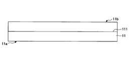
- FIG. 4 is an explanatory diagram of a configuration example of a side surface of a base made of an inorganic material.
- FIG. 2 is an explanatory diagram of a configuration of an optical package according to the embodiment.
- the window material of the present embodiment is a window material for an optical package provided with an optical element, and is disposed along an outer periphery of the inorganic material substrate on one surface of the inorganic material substrate and the inorganic material substrate. And a bonding layer formed. Then, the width of the bonding layer can be 0.2 mm or more and 2 mm or less, and the thickness of the bonding layer can be more than 15 ⁇ m and 100 ⁇ m or less.
- FIG. 1A is a schematic cross-sectional view of a window material 10 of the present embodiment taken along a plane parallel to the laminating direction of a base 11 made of an inorganic material and a bonding layer 12.
- FIG. 1B shows a structure when the window member 10 shown in FIG. 1A is viewed along a block arrow A shown in FIG. 1A. That is, a bottom view of the window material 10 shown in FIG.
- the window material 10 of the present embodiment has a base 11 made of an inorganic material and a bonding layer 12.
- the bonding layer 12 can be disposed on one surface 11a of the inorganic material base 11.
- the one surface 11a of the inorganic material base 11 corresponds to a surface to be joined to a circuit board having an optical element when an optical package described later is manufactured. That is, the one surface 11a of the base 11 made of an inorganic material can be said to be a surface facing the optical element.
- the other surface 11b of the inorganic material base 11 opposite to the one surface 11a is a surface exposed to the outside when an optical package is formed.
- the substrate 11 made of an inorganic material is not particularly limited, and may be made of any material and formed into any shape.
- the substrate 11 made of an inorganic material is an optical package
- the light in a wavelength region that is required to be particularly transmitted (hereinafter referred to as “light in a desired wavelength region”) of the light related to the optical element provided in the circuit board.
- the transmittance is preferably 50% or more, more preferably 70% or more, still more preferably 80% or more, and particularly preferably 90% or more.
- the transmittance of the inorganic material base 11 is preferably 50% or more, and more preferably 70% or more for light having a wavelength of 0.7 ⁇ m or more and 1 mm or less. It is more preferably at least 80%, particularly preferably at least 90%.
- the base material 11 made of an inorganic material has a transmittance of 50% or more for light having a wavelength in the range of 380 nm to 800 nm, for example. It is preferably at least 70%, more preferably at least 80%, particularly preferably at least 90%.
- the transmittance of the inorganic material base 11 is preferably 50% or more, more preferably 70% or more, for light having a wavelength in the range of 200 nm to 380 nm. It is more preferably at least 80%, particularly preferably at least 90%.
- the transmittance of the inorganic material base 11 is preferably 50% or more, and more preferably 70% or more, for light having a wavelength in the range of 315 nm to 380 nm. Is more preferable, 80% or more is further preferable, and 90% or more is particularly preferable.
- the transmittance of the inorganic material substrate 11 is preferably 50% or more, and more preferably 70% or more for light having a wavelength in the range of 280 nm to 315 nm. Is more preferable, 80% or more is further preferable, and 90% or more is particularly preferable.
- the transmittance of the inorganic material substrate 11 is preferably 50% or more, and more preferably 70% or more for light having a wavelength in the range of 200 nm to 280 nm. Is more preferable, 80% or more is further preferable, and 90% or more is particularly preferable.
- the transmittance of the inorganic material base 11 can be measured according to JIS K 7361-1 (1997).
- the material of the inorganic material base 11 can be arbitrarily selected as described above, and is not particularly limited. From the viewpoint of particularly enhancing hermetic sealing and durability, for example, quartz, Glass or the like can be preferably used. Quartz includes quartz glass and those containing 90% by mass or more of SiO 2 . Examples of the glass include soda lime glass, aluminosilicate glass, borosilicate glass, non-alkali glass, crystallized glass, and high refractive index glass (nd ⁇ 1.5). The material of the inorganic base material is not limited to one kind, and two or more kinds of materials can be used in combination.
- the material of the substrate 11 made of an inorganic material is selected from, for example, quartz, soda lime glass, aluminosilicate glass, borosilicate glass, alkali-free glass, crystallized glass, and high refractive index glass (nd ⁇ 1.5).
- quartz soda lime glass
- aluminosilicate glass borosilicate glass
- alkali-free glass crystallized glass
- high refractive index glass (nd ⁇ 1.5) is selected from, for example, quartz, soda lime glass, aluminosilicate glass, borosilicate glass, alkali-free glass, crystallized glass, and high refractive index glass (nd ⁇ 1.5).
- nd ⁇ 1.5 high refractive index glass
- the inorganic material base 11 may be subjected to a chemical strengthening treatment.
- the thickness of the inorganic material base 11 is not particularly limited, but is preferably, for example, 0.03 mm or more, more preferably 0.05 mm or more, and even more preferably 0.1 mm or more. , 0.3 mm or more is particularly preferable.
- the thickness of the inorganic material substrate 11 By setting the thickness of the inorganic material substrate 11 to 0.03 mm or more, the strength required for the optical package is sufficiently exhibited, and moisture and the like pass through the surface of the window material inorganic material substrate 11 to the optical element. It is possible to particularly suppress transmission to the side on which the arrangement is performed.
- the thickness of the inorganic material base 11 By setting the thickness of the inorganic material base 11 to 0.3 mm or more as described above, the strength of the optical package can be particularly increased, which is preferable.
- the upper limit of the thickness of the inorganic material base 11 is not particularly limited, but is preferably, for example, 5 mm or less, more preferably 3 mm or less, and further preferably 1 mm or less. This is because the transmittance of light in a desired wavelength region can be sufficiently increased by setting the thickness of the inorganic material base 11 to 5 mm or less. It is more preferable to set the thickness of the inorganic material base 11 to 1 mm or less, particularly since the height of the optical package can be reduced.
- FIG. 1A shows an example of a plate-like shape (a flat plate shape) as the inorganic material base 11, but the present invention is not limited to such a shape.
- the shape of the inorganic material base 11 is not particularly limited, and the thickness does not need to be uniform. For this reason, when the thickness of the inorganic material base is not uniform, it is preferable that the thickness of the portion of the inorganic material base on the optical path of light related to the optical element when at least an optical package is in the above range, It is more preferable that the thickness of the inorganic material substrate is in the above range at any portion.
- the shape of the inorganic material base 11 is not particularly limited as described above.
- the shape may be a plate-like shape or a shape in which the lens is integrated, that is, a shape including concave portions and convex portions derived from the lens.
- one surface 11a of the base 11 made of an inorganic material is a flat surface, and the other surface 11b has a convex portion or a concave portion, or the shape of the one surface 11a and the shape of the other surface 11b are different. Is the reverse of the embodiment.
- one surface 11a of the base 11 made of an inorganic material has a convex portion and the other surface 11b has a concave portion, or a configuration in which the shape of the one surface 11a and the shape of the other surface 11b are opposite to each other.
- Form there is a form in which each of the one surface 11a and the other surface 11b of the inorganic material base 11 has a convex portion or a concave portion.
- the portion where the bonding layer 12 is disposed on the one surface 11a of the inorganic material base 11 is, for example, a plurality of window materials. It is preferable that the surface is flat in order to suppress the variation of the shape of the bonding layer 12 between the window materials when, for example, is manufactured.
- the size of the inorganic material base may become very small. Therefore, it is preferable to employ a cutting method using laser light when cutting the inorganic material base material to a desired size before cutting. Then, when cutting is performed by such a method, as shown in FIG. 2, the side surface of the base material 11 made of an inorganic material corresponds to the focal position of the laser beam and has a linear pattern along the outer periphery of one surface 11a. 111.
- the method of cutting the inorganic material base 11 is not limited to the above-described example, but may be cut by any method.
- the side surface of the inorganic material base 11, that is, the cut surface may have a cross-sectional shape different from the above-described case.
- Other cutting methods include, for example, a dicing saw and a wire saw. These cutting methods are effective when the thickness of the inorganic material base before cutting is 1 mm or more.
- An antireflection film may be provided on the surface of the inorganic material base 11.
- the anti-reflection film By arranging the anti-reflection film, in the case of an optical package, the optical element or the light from the outside is prevented from being reflected on the surface of the inorganic material base 11, and the optical element or the light from the outside is suppressed.
- the transmittance can be increased, which is preferable.
- the antireflection film is not particularly limited.
- a multilayer film can be used, and the multilayer film is made of alumina (aluminum oxide, Al 2 O 3 ), hafnium oxide (HfO 2 ), or titanium oxide (TiO 2 ).
- first layer which is a layer of one or more materials selected from the group consisting of one or more materials
- second layer which is a layer of silica (silicon oxide, SiO 2 )
- the number of layers constituting the multilayer film is not particularly limited, for example, the first layer and the second layer are set as one set, and the multilayer film is formed as one set of the first layer and the second layer. Preferably, it has at least two pairs, and more preferably, at least two pairs. This is because, when the multilayer film has at least one set of the first layer and the second layer, reflection of light on the surface of the inorganic material base 11 can be particularly suppressed.
- the upper limit of the number of layers constituting the multilayer film is not particularly limited. For example, from the viewpoint of productivity and the like, it is preferable to have four or less sets of the first layer and the second layer.
- the anti-reflection film is preferably disposed on at least one surface 11a of the inorganic material base 11, and more preferably on both surfaces of one surface 11a and the other surface 11b.
- the configurations of the two anti-reflection films may be different. However, from the viewpoint of productivity and the like, it is necessary to have the same configuration. Is preferred.
- the second layer of silica is located on the outermost surface. Since the second layer of silica is located on the outermost surface of the anti-reflection film, the surface of the anti-reflection film has a composition similar to that of the glass substrate, and the durability and the adhesion to the bonding layer 12 are particularly high. This is because it is preferable.
- the bonding layer 12 serves as a member for bonding the inorganic material base 11 and a circuit board having an optical element when forming an optical package.
- the shape of the bonding layer 12 is not particularly limited, for example, as shown in FIG. 1B, the view when viewed from the side where the bonding layer 12 is formed of the window material 10, that is, the solder layer in the bottom view
- the bonding layer 12 including 122 can be formed in a shape arranged along the outer periphery of the inorganic material base 11. That is, the bonding layer 12 can have, for example, a strip shape arranged along the outer periphery of the inorganic material base 11.
- the bonding layer 12 has an opening in the center corresponding to the optical element of the circuit board, and can be formed into a shape in which the inorganic material base 11 can be seen from the opening. In FIG.
- the substrate 11 made of an inorganic material is larger than the bonding layer 12 including the solder layer 122, but the present invention is not limited to this.
- the outer periphery of the base material 11 made of an inorganic material and the outer periphery of the bonding layer 12 including the solder layer 122 may be configured to coincide.
- FIG. 1B shows the solder layer 122 located on the outermost surface of the bonding layer 12, a plane perpendicular to the lamination direction of the layers of the bonding layer 12 (the vertical direction in FIG. 1A). It is preferable that the cross-sectional shape of the bonding layer 12 be the same regardless of the layer.
- the width (line width) W of the bonding layer 12 is set to be 0.2 mm or more and 2 mm or less, and the thickness T of the bonding layer 12 is set to be more than 15 ⁇ m and 100 ⁇ m or less. Is preferred.
- the width W of the bonding layer 12 is, as shown in FIG. 1B, the width of the band-shaped bonding layer 12 when viewed from the upper surface or the lower surface of the inorganic material base 11.
- the width W of the bonding layer 12 means a distance between the outer peripheral side surface 12A and the inner peripheral side surface 12B measured along a line segment perpendicular to the inner peripheral side surface 12B of the bonding layer 12.
- the thickness T of the bonding layer 12 means the thickness of the bonding layer 12 in the laminating direction (the vertical direction in FIG. 1A) between the inorganic material base 11 and the bonding layer 12.
- the thickness T is measured along a line segment perpendicular to one surface 11a of the inorganic material base 11.
- the width W and the thickness T of the bonding layer 12 satisfy the above ranges when the bonding layer 12 is measured at an arbitrary position. That is, it is preferable that the above range be satisfied regardless of the position of the bonding layer 12 measured.
- the bonding layer 12 can include a base metal layer 121 and a solder layer 122 as described later.
- the bonding layer 12 and the inorganic material base 11 are heated and cooled. May be.
- the substrate 11 made of an inorganic material and the bonding layer 12 are formed of different materials, and have different degrees of expansion and contraction during heating and cooling. Therefore, when the bonding layer 12 is formed, residual stress may occur at the interface between the inorganic material base 11 and the bonding layer 12. According to the study of the inventors of the present invention, it is inferred that such residual stress causes a crack in the window material when the window material and the circuit board having the optical element are joined. You.
- the generation of the residual stress is suppressed by setting the width W and the thickness T of the bonding layer 12 within the predetermined ranges as described above.
- the width W of the bonding layer 12 is preferably equal to or less than 0.6 mm, and more preferably equal to or less than 0.4 mm.
- the width W of the bonding layer 12 is 0.2 mm or more. And more preferably 0.25 mm or more.
- the thickness T of the bonding layer 12 is more preferably 50 ⁇ m or less, and further preferably 30 ⁇ m or less.
- the thickness T of the bonding layer 12 is preferably larger than 15 ⁇ m.
- the distance D between the outer peripheral side surface 11A of the inorganic material base 11 and the outer peripheral side surface 12A of the bonding layer 12 is not particularly limited, but reduces the residual stress generated at the outer peripheral edge of the bonding layer after the application of the bonding layer. Therefore, it is preferably 0.5 mm or less, more preferably 0.3 mm or less, and even more preferably 0.1 mm or less.
- the lower limit value of the distance D between the outer peripheral side surface 11A of the inorganic material base 11 and the outer peripheral side surface 12A of the bonding layer 12 is not particularly limited. As described above, since the outer periphery of the inorganic material base 11 and the outer periphery of the bonding layer 12 including the solder layer 122 can be configured to coincide with each other, for example, the distance D can be 0 or more. .
- the distance D between the outer peripheral side surface 11A of the inorganic material base 11 and the outer peripheral side surface 12A of the bonding layer 12 is, for example, as shown in FIG. It means the distance between the outer peripheral side surface 11A and the outer peripheral side surface 12A of the bonding layer 12 disposed along the outer peripheral side surface 11A of the inorganic material base 11. That is, when a straight line perpendicular to the outer peripheral side surface 11A of the inorganic material base 11 is drawn in the bottom view as shown in FIG. It means the shortest distance between the layer 12 and the outer peripheral side surface 12A.
- the distance D between the outer peripheral side surface 11A of the inorganic material base 11 and the outer peripheral side surface 12A of the bonding layer 12 is the distance between the outer peripheral side surface 11A of the inorganic material base 11 and the bonding layer 12 at a position corresponding to this. It is preferable that the above range is satisfied when measured at an arbitrary position with respect to the outer peripheral side surface 12A. That is, the outer peripheral side surface 11A of the inorganic material base 11 and the outer peripheral side surface 12A of the bonding layer 12 at a position corresponding to the outer peripheral side surface 11A preferably satisfy the above range when measured at any location.
- the bonding layer 12 may be any member as long as it can bond the inorganic material base 11 and the circuit board having the optical element, and the material or the like forming the bonding layer 12 is not particularly limited. However, for example, it is preferable to select the material and the shape of the bonding layer so that the parameter Z calculated by the following equation (1) is 130 or less, and the material and the shape of the bonding layer are selected so as to be 100 or less. Is more preferable.
- x0, x1, x2, x3, x4, and x5 in the above equation (1) indicate the following parameters, respectively.
- x3 Thermal expansion coefficient (ppm / ° C) of the bonding layer at 20 ° C or more and 200 ° C or less.
- x4 average height of bonding layer (mm)
- x5 width of bonding layer (mm)
- x4 average height of the bonding layer
- x5 width of bonding layer
- Young's modulus can be calculated from the results of tests based on JISZ2241 (2011) “Test method for tensile strength of metallic materials” and JISR1602 (1995) “Test method for elastic modulus of fine ceramics”. Further, the thermal expansion coefficient is calculated according to JISZ2285 (2003) “Method of measuring linear expansion coefficient of metal material”, JISR3102 (1995) “Test method of average linear expansion coefficient of glass”, and the like.
- the lower limit of the parameter Z is not particularly limited, but is preferably 10 or more.
- the bonding layer 12 may be any member that can bond the inorganic material base 11 and the circuit board having the optical element, and the specific layer configuration is not particularly limited. However, it is preferable that the bonding layer 12 be made of a metal material from the viewpoint of increasing the airtightness when the optical package is formed. For example, as shown in FIG. , And a solder layer 122.
- the base metal layer 121 can have a function of enhancing the adhesion between the inorganic material base 11 and the solder layer 122.
- the configuration of the base metal layer 121 is not particularly limited, but preferably includes a plurality of layers as shown in FIG.
- the configuration of the base metal layer 121 is not particularly limited, but may be composed of, for example, two or three layers. Specifically, for example, a first base metal layer 121A and a second base metal layer 121B can be provided in order from the inorganic material base 11 side. Further, a third base metal layer 121C may be further disposed between the second base metal layer 121B and the solder layer 122.
- the first underlying metal layer 121A can have a function of improving the adhesion between the inorganic material base 11 and another layer.
- the material of the first base metal layer 121A is preferably a material capable of improving the adhesion between the inorganic material base 11 and another layer, and more preferably a material capable of improving the airtightness.
- the first underlying metal layer 121A is preferably a layer containing at least one selected from chromium (Cr), titanium (Ti), tungsten (W), and palladium (Pd), for example.
- the first base metal layer 121A may be a layer made of at least one material selected from, for example, chromium (Cr), titanium (Ti), tungsten (W), and palladium (Pd). Note that even in this case, it does not exclude that the first base metal layer 121A contains unavoidable impurities.
- the first base metal layer 121A is preferably a metal film or a metal oxide film of at least one metal selected from chromium (Cr), titanium (Ti), tungsten (W), and palladium (Pd). preferable.
- the second base metal layer 121B has a function of improving the adhesion between the solder layer and another layer, and is selected from, for example, nickel (Ni), copper (Cu), platinum (Pt), and silver (Ag).
- the layer contains at least one kind of metal.
- the second base metal layer 121B is more preferably a layer containing at least one metal selected from nickel (Ni) and copper (Cu).
- the second base metal layer 121B may be a layer made of at least one metal selected from, for example, nickel (Ni), copper (Cu), platinum (Pt), and silver (Ag). Also in this case, from the viewpoint of cost, it is preferable that the second base metal layer 121B be a layer made of at least one metal selected from nickel (Ni) and copper (Cu). In any case, it does not exclude that the second base metal layer 121B contains unavoidable impurities.
- the third underlayer metal layer 121C is preferably a layer containing at least one selected from nickel (Ni) and gold (Au), for example.
- the third base metal layer 121C is a layer containing nickel (Ni), a layer containing a nickel-boron alloy (Ni-B) or a layer containing Ni-B to improve solder wettability. It is preferable that By providing the third base metal layer 121C, for example, the reaction between the base metal layer 121 and the solder layer 122 can be particularly suppressed.
- the third base metal layer may be a layer made of at least one metal selected from nickel (Ni) and gold (Au). Even in this case, it does not exclude that the third base metal layer contains unavoidable impurities.
- each layer constituting the base metal layer 121 is not particularly limited and can be arbitrarily selected.
- the thickness of the first base metal layer 121A is preferably 0.03 ⁇ m or more from the viewpoint of particularly increasing the adhesion of the inorganic material to the base 11.
- the upper limit of the thickness of the first base metal layer 121A is not particularly limited, but is preferably 0.2 ⁇ m or less from the viewpoint of sufficiently reducing the cost.
- the thickness of the second base metal layer 121B is preferably 0.1 ⁇ m or more from the viewpoint of particularly increasing the adhesion to the solder layer 122.
- the upper limit of the thickness of the second base metal layer 121B is not particularly limited, but is preferably 2.0 ⁇ m or less from the viewpoint of sufficiently reducing the cost.
- the third base metal layer 121C When the third base metal layer 121C is also provided, its thickness is not particularly limited, but is preferably, for example, 0.05 ⁇ m or more from the viewpoint of particularly suppressing the reaction between the base metal layer 121 and the solder layer 122.
- the upper limit of the thickness of the third base metal layer is not particularly limited, but is preferably 1.0 ⁇ m or less from the viewpoint of sufficiently reducing the cost.
- solder layer 122 Next, the solder layer 122 will be described.
- the solder layer 122 has a function of bonding the inorganic material base 11 and a circuit board having an optical element when manufacturing an optical package, and the configuration thereof is not particularly limited.
- the solder layer 122 may include solder as described below, and the solder as used herein is melted by heating at the time of joining with a circuit board having an optical element, and then cooled by cooling.
- a material that can form an intermetallic compound with a material disposed on a joining surface of a circuit board having an optical element and that can be joined It is preferred that
- the thickness of the solder layer 122 is not particularly limited, but is preferably 5 ⁇ m or more, and more preferably 15 ⁇ m or more.
- the insulating base material of the circuit board can be formed of, for example, a ceramic material as described later. However, when manufactured from a ceramic material, since it is usually a casting, it is not possible to completely flatten the surface to be joined to the window material 10. Often difficult. Therefore, it is preferable that the thickness of the solder layer is set to 5 ⁇ m or more so as to absorb the unevenness of the surface of the insulating base material that is joined to the window material 10.
- the thickness of the solder layer 122 here means the thickness of the solder layer 122 at an arbitrary position of the window material 10 of the present embodiment. Therefore, it is preferable that the solder layer satisfies such a thickness range even in the thinnest part.
- the upper limit of the thickness of the solder layer is not particularly limited, but may be, for example, 50 ⁇ m or less.
- the average value of the thickness of the solder layer 122 is preferably 5 ⁇ m or more, more preferably 15 ⁇ m or more. This is because the average value of the thickness of the solder layer 122 is 5 ⁇ m or more, so that even if the bonding surface of the circuit board to be bonded to the bonding layer 12 has irregularities, the concave portion is filled with the material of the solder layer. In particular, the hermetic sealing can be improved.
- the above average means a simple average (sometimes called an arithmetic average or an arithmetic average).
- a simple "average” means a simple average.
- the upper limit of the average value of the thickness of the solder layer 122 is not particularly limited, but is preferably 50 ⁇ m or less, and more preferably 30 ⁇ m or less. This is because even if the average value of the thickness of the solder layer 122 exceeds 50 ⁇ m and becomes excessively thick, the effect of hermetic sealing does not greatly change.
- the average value of the thickness of the solder layer 122 can be calculated by measuring the thickness of the solder layer 122 at a plurality of arbitrary measurement points with a laser microscope (manufactured by Keyence Corporation, Model VK-8510) and calculating the average value.
- the number of measurement points for measuring the thickness of the solder layer 122 for calculating the average value is not particularly limited, for example, two or more points are preferable, and four or more points are more preferable.
- the upper limit of the number of measurement points is not particularly limited, but is preferably 10 or less, more preferably 8 or less from the viewpoint of efficiency.
- the thickness deviation of the solder layer 122 that is, the deviation from the simple average value of the thickness is preferably within ⁇ 20 ⁇ m, more preferably within ⁇ 10 ⁇ m.
- the airtight sealing property between the window material and the circuit board on which the optical element is arranged can be particularly enhanced when the optical package is manufactured. It is possible and preferable.
- the deviation of the thickness of the solder layer 122 within ⁇ 20 ⁇ m means that the deviation is distributed in a range from ⁇ 20 ⁇ m to +20 ⁇ m.
- the deviation of the thickness of the solder layer 122 can be calculated from the average value of the thickness of the solder layer described above and the measured value used in calculating the average value.
- the solder layer 122 can contain various solders (composition for bonding) and can also be made of various solders.
- the solder included in the solder layer 122 is not particularly limited, but for example, a material having a Young's modulus of 50 GPa or less is preferable, a material of 40 GPa or less is more preferable, and a material of 30 GPa or less is further preferable.
- the temperature of the solder layer may change.
- the Young's modulus of the solder contained in the solder layer is set to 50 GPa or less, a temperature change occurs in the solder layer portion, and even when the solder layer expands and contracts, other members such as the inorganic material base 11 can be broken. Is particularly preferred because it is possible to suppress
- the Young's modulus of the solder is 50 GPa or less
- the stress generated due to the difference in thermal expansion between the inorganic material base 11 and the circuit board provided with the optical element is caused by the solder layer joining the two members. This is because it can be absorbed in the region 122 and is preferable.
- the lower limit of the preferred range of the Young's modulus of the solder contained in the solder layer 122 is not particularly limited, but may be, for example, greater than 0, and is preferably 10 GPa or more from the viewpoint of improving hermetic sealing.
- the melting point of the solder contained in the solder layer 122 is preferably 200 ° C. or higher, more preferably 230 ° C. or higher. This is because when the melting point of the solder is 200 ° C. or higher, the heat resistance of the optical package can be sufficiently increased.
- the melting point of the solder used for the solder layer 122 is preferably 280 ° C. or less. This means that when the optical package is manufactured, heat treatment is performed and at least a part of the solder layer 122 is melted.
- the melting point of the solder is 280 ° C. or less, the temperature of the heat treatment can be suppressed to a low level. This is because it is possible to particularly suppress the occurrence of damages. Also, by suppressing the heat treatment temperature to be low, it is possible to reduce the difference in the degree of shrinkage due to the difference in the coefficient of thermal expansion between the material of the inorganic base 11 and the insulating material of the circuit board.
- the solder contained in the solder layer 122 preferably has a density of 6.0 g / cm 3 or more, more preferably 7.0 g / cm 3 or more. This is because, by setting the density of the solder used for the solder layer 122 to 6.0 g / cm 3 or more, the hermetic sealing property can be particularly improved.
- the upper limit of the density of the solder used for the solder layer 122 is not particularly limited, but is preferably, for example, 10 g / cm 3 or less.
- the coefficient of thermal expansion of the solder included in the solder layer 122 has a predetermined relationship with the coefficient of thermal expansion of the inorganic material base 11. Specifically, it is preferable that the difference between the coefficient of thermal expansion of the inorganic material base and the coefficient of thermal expansion of the solder contained in the solder layer is small. More specifically, the difference between the coefficient of thermal expansion of the inorganic material base 11 and the coefficient of thermal expansion of the solder contained in the solder layer 122 at 20 ° C. or more and 200 ° C. or less is preferably 30 ppm / ° C. or less, and more preferably 10 ppm. / ° C or lower.
- the difference between the thermal expansion coefficient of the inorganic material base 11 and the thermal expansion coefficient of the solder included in the solder layer is small, the residual stress generated between the inorganic material base 11 and the bonding layer 12 is suppressed. This is because, when bonded to a circuit board, it is possible to particularly suppress the occurrence of cracks.
- the difference between the coefficient of thermal expansion of the inorganic material base and the coefficient of thermal expansion of the solder contained in the solder layer can be zero or more.
- the thermal expansion coefficient of the solder contained in the solder layer 122 is not particularly limited, but the thermal expansion coefficient is preferably 30 ppm / ° C. or less, more preferably 25 ppm / ° C. or less. This is because when the thermal expansion coefficient of the solder is 30 ppm / ° C. or less, the optical package is used, and the shape change due to heat generated when the optical element emits light is suppressed, and the optical package can be more reliably prevented from being damaged. It is.
- the lower limit of the thermal expansion coefficient of the solder contained in the solder layer 122 is not particularly limited, but is preferably, for example, 0.5 ppm / ° C. or more.
- the solder that can be preferably used for the solder layer 122 is not particularly limited.
- tin (Sn) -germanium (Ge) -nickel (Ni) -based solder or tin (Sn) -antimony One or more types selected from Sb) -based solder, gold (Au) -tin (Sn) -based solder, tin (Sn) -silver (Ag) -copper (Cu) -based solder, and the like can be given.
- tin can be contained as a main component.
- To contain tin as a main component means, for example, that it is the component most contained in the solder, and it is preferable that tin is contained in the solder in an amount of 60% by mass or more.
- the tin content of the solder is, for example, preferably 85.9% by mass or more, more preferably 87.0% by mass or more, and particularly preferably 88.0% by mass or more.
- the upper limit of the tin content in the solder is not particularly limited, but is, for example, preferably 99.9% by mass or less, more preferably 99.5% by mass or less, and even more preferably 99.3% by mass or less.
- the tin-germanium-nickel solder may further contain one or more components selected from iridium, zinc, and the like, in addition to tin, germanium, and nickel.
- the content of each component of the tin-antimony solder is not particularly limited.
- the content of antimony is preferably 1% by mass or more.
- Antimony has a function of increasing the solidus temperature in the tin-antimony solder, and by setting the content of antimony to 1% by mass or more, such an effect can be particularly exhibited, which is preferable.
- the upper limit of the content of antimony is not particularly limited, but is preferably, for example, 40% by mass or less. This is because by setting the content of antimony to 40% by mass or less, the solidus temperature can be prevented from becoming excessively high, and a solder suitable for mounting electronic components can be obtained.
- the tin-antimony solder can contain tin. Tin can reduce the difference in thermal expansion between the solder and a member to be joined such as a circuit board or a base metal layer. Further, by containing tin as a main component of the solder, the melting point temperature of the solder can be set to about 230 ° C., which is the melting point temperature of tin.
- the tin-antimony solder can also be composed of antimony and tin.
- the remainder excluding antimony can be composed of tin.
- the tin-antimony solder can contain any additional components other than antimony and tin, and can also contain, for example, one or more selected from silver (Ag), copper (Cu), and the like. Silver and copper have a function of raising the solidus temperature of the solder similarly to antimony. In this case, the remainder other than antimony and any additional components can be composed of tin.
- solder used for the solder layer 122 is not limited to such solder as described above.
- the residual stress at the interface between the inorganic material base 11 and the bonding layer 12 is preferably 100 MPa or less, more preferably 50 MPa or less.
- the lower limit value can be set to 0, for example.
- the residual stress is preferably 10 MPa or more.
- the bonding layer has a predetermined size. For this reason, the residual stress at the interface between the inorganic material base and the bonding layer can be suppressed, and the occurrence of cracks in the window material, specifically, the inorganic material base when bonded to the circuit board can be suppressed.
- the method for manufacturing the window material of the present embodiment is not particularly limited, but may include, for example, the following steps.
- the specific operation of the substrate preparation step is not particularly limited, for example, the inorganic material substrate can be cut to have a desired size, or the inorganic material substrate can be processed to have a desired shape.
- the antireflection film can be formed in this step.
- the method for forming the antireflection film is not particularly limited, and for example, a film can be formed by a dry method or a wet method.
- an evaporation method, a sputtering method, an ion plating method, or the like is used.
- a film can be formed by one or more methods selected from an immersion method, a spray coating method, and the like.
- the bonding layer forming step may include, for example, a base metal layer forming step of forming a base metal layer, and a solder layer forming step.
- the base metal layer can be formed on one surface of the inorganic material base.
- the method for forming the base metal layer is not particularly limited, and can be arbitrarily selected according to the type of the base metal layer to be formed.
- a film can be formed by a dry method or a wet method.
- a film can be formed by one or more methods selected from an evaporation method, a sputtering method, an ion plating method, and the like.
- a film can be formed by one or more methods selected from an electrolytic plating method, an electroless plating method, a printing method, and the like.
- the base metal layer can be composed of a plurality of layers, and can be formed for each layer by an arbitrary method.
- a solder layer can be formed on one surface of the inorganic material base or on the base metal layer.
- the method for forming the solder layer is not particularly limited, and includes, for example, one or more types selected from a dip method, a coating method using a dispenser, a printing method, a laser metal deposition method, a method using a solder wire, and the like. .
- solder as a raw material of a solder layer is melted in a solder melting tank, and a member for forming a solder layer, for example, a portion for forming a solder layer of a base of an inorganic material on which a base metal layer is arranged is soldered.
- a solder layer is formed by dipping in molten solder in a melting bath.
- the application method using a dispenser for example, from a dispenser connected with a syringe, supplying a molten solder to a member forming a solder layer, for example, a portion of the inorganic material base on which a base metal layer is disposed, where a solder layer is formed, This is a method of forming a solder layer.
- the printing method is a method in which a paste-like solder is printed on a member for forming a solder layer, for example, a portion of a base made of an inorganic material on which a base metal layer is disposed, where the solder layer is to be formed, to form a solder layer. After the printing, heat treatment can be performed if necessary.
- a powdery solder is supplied to a member for forming a solder layer, for example, a portion of a base made of an inorganic material on which a base metal layer is disposed, where a solder layer is formed, and the laser is used to melt the solder.
- a solder layer by cooling.
- the method using a solder wire uses a wire-shaped, that is, a solder processed in a linear shape, and for example, by an automatic soldering robot or the like, a member for forming a solder layer, for example, a solder layer of an inorganic material base on which a base metal layer is disposed. This is a method in which molten solder is supplied to a portion where a solder layer is to be formed to form a solder layer.
- the method for manufacturing a window material according to the present embodiment may further include an optional step as needed.
- the bonding layer can be formed on one surface 11a of the inorganic material base 11 so as to have a desired shape.
- the method for manufacturing a window material includes, for example, a method of forming a bonding layer by a base metal layer forming step and a solder layer forming step, and then patterning the bonding layer into a desired shape. It can also have a activating step.
- a resist corresponding to the pattern to be formed is arranged on the exposed surface of the solder layer, and a portion of the solder layer and the underlying metal layer that is not covered with the resist is removed by etching or the like. Can be patterned.
- a resist removing step of removing the resist may be performed.
- a patterning step is performed after forming a part of the layer included in the base metal layer, and a part of the layer included in the formed base metal layer is formed. Can also be patterned. Then, after performing the resist removing step of removing the resist after the patterning step, the remaining underlying metal layer may be further formed on the patterned underlying metal layer.
- the method for manufacturing a window material according to the present embodiment includes a resist disposing method in which a resist is disposed on a portion where a solder metal layer is not formed, before performing a solder metal layer forming step and a solder metal layer forming step. It can also have steps.
- a resist removing step of removing the resist after the solder layer forming step may be provided.
- the inorganic material A cutting step for cutting the substrate may be included.
- the cutting method is not particularly limited, and a cutting method suitable for an inorganic material base, such as the above-described cutting method using laser light, can be employed.
- the joining layer is formed continuously in the adjacent window material, that is, when the joining layer is arranged on the cutting line, the joining layer can also be cut in the cutting step.
- optical package Next, one configuration example of the optical package of the present embodiment will be described.
- the optical package of the present embodiment can include the above-described window material and a circuit board provided with an optical element.
- FIG. 3 is a schematic cross-sectional view of a window member of the optical package of the present embodiment and a circuit board provided with an optical element, taken along a plane parallel to the laminating direction.
- the window member 10 and the circuit board 31 are separately illustrated so as to be distinguished from each other.
- both members are joined and integrated.
- the optical package 30 of the present embodiment includes the above-described window material 10 and the circuit board 31 including the optical element 32.
- the circuit board 31 is not particularly limited, and various circuit boards including an insulating base material 311 and wiring (not shown) for supplying power to the optical element 32 can be used.
- the circuit board 31 when the window material 10 is joined, the circuit board 31 must have an insulating base material 311 made of ceramics in order to improve the hermetic sealing in the space surrounded by the window material 10 and the circuit board 31. Is preferred.
- the ceramic material used for the insulating base material 311 of the circuit board 31 is not particularly limited.
- alumina aluminum oxide, Al 2 O 3
- aluminum nitride AlN
- LTCC Low Temperature Co-fired Ceramics
- the shape of the insulating base material 311 of the circuit board 31 is not particularly limited, when the optical package 30 is used, the optical element 32 is arranged by the base material 11 of the inorganic material, the insulating base material 311, and a bonding portion described later. It is preferable that it is configured so that a closed space can be formed in a portion where the pressure is reduced. For this reason, it is preferable that the insulating base material 311 has an opening at the center of the upper surface 311a, and has a concave portion 311A that is a non-through hole including the opening. Note that the upper surface of the insulating base material 311 is a surface facing the window material 10 in the case of an optical package, and can also be referred to as a surface to be joined to the window material 10.
- the wall 311B surrounding the recess 311A supports the bonding layer 12 of the window material 10 and a base metal layer for a circuit board, which will be described later, in the case of an optical package. It can have a shape corresponding to the base metal layer for use.
- the circuit board 31 may have a circuit board base metal layer 312 on the upper surface 311a of the insulating base material 311 and on the upper surface of the wall 311B.
- the circuit board base metal layer 312 can have a function of increasing the adhesion between the insulating base material 311 of the circuit board 31 and the window material 10.
- a specific configuration of the circuit board base metal layer 312 is not particularly limited, for example, the first circuit board base metal layer 312A and the second circuit board base metal layer 312B from the insulating substrate 311 side of the circuit board 31.
- a third circuit board base metal layer 312C is shown here, the present invention is not limited to such an embodiment, and the circuit board base metal layer 312 may be formed of one layer, two layers, or four or more layers.
- the first circuit board base metal layer 312A is made of the same metal as the metal used to form the wiring (circuit) on the circuit board 31. It is preferable to configure.
- the first circuit board base metal layer 312A can be a layer containing one or more metals selected from copper (Cu), silver (Ag), and tungsten (W).
- the first circuit board base metal layer 312A may be a layer made of at least one metal selected from copper (Cu), silver (Ag), and tungsten (W). Even in this case, it does not exclude that the first circuit board base metal layer 312A contains unavoidable impurities.
- the second circuit board base metal layer 312B can be a layer that prevents the later-described third circuit board base metal layer 312C and the first circuit board base metal layer 312A from being alloyed. It can be a layer containing (Ni).
- the second circuit board base metal layer 312B may be a layer made of nickel (Ni). Note that even in this case, it does not exclude that the second circuit board base metal layer 312B contains unavoidable impurities.
- the third circuit board base metal layer 312C can be a layer for preventing the second circuit board base metal layer 312B from being oxidized, and can be, for example, a layer containing gold (Au).
- the third circuit board base metal layer 312C may be a layer made of gold (Au). Even in this case, it does not exclude that the third circuit board base metal layer 312C contains unavoidable impurities.
- each layer constituting the circuit board base metal layer 312 is not particularly limited and can be arbitrarily selected.
- the thickness of the first circuit board base metal layer 312A is preferably, for example, 1 ⁇ m or more.
- the upper limit of the thickness of the first circuit board base metal layer 312A is not particularly limited, but is preferably 20 ⁇ m or less from the viewpoint of sufficiently reducing the cost.
- the thickness of the second circuit board base metal layer 312B is preferably 1 ⁇ m or more from the viewpoint of particularly suppressing alloying between the first circuit board base metal layer 312A and the third circuit board base metal layer 312C.
- the upper limit of the thickness of the second circuit board base metal layer 312B is not particularly limited, but is preferably 20 ⁇ m or less from the viewpoint of sufficiently reducing costs.
- the thickness of the third circuit board base metal layer 312C is preferably 0.03 ⁇ m or more from the viewpoint of particularly preventing oxidation of the other circuit board base metal layer.
- the upper limit of the thickness of the third circuit board base metal layer 312C is not particularly limited, it is preferably 2.0 ⁇ m or less, more preferably 0.5 ⁇ m or less, from the viewpoint of sufficiently reducing costs.
- the shape of the circuit board base metal layer 312 is not particularly limited, either. However, when the optical package 30 is used, a bonding portion 33 described later is formed together with the bonding layer 12 of the window material 10. Preferably, it has a corresponding shape.
- the bonding layer 12 of the window member 10 and the base metal layer 312 for a circuit board have a cross-sectional shape in a plane perpendicular to the laminating direction (vertical direction in FIG. 3) of both members when forming an optical package. Preferably they have the same shape.
- the method of forming the circuit board base metal layer 312 is not particularly limited, and can be arbitrarily selected according to, for example, the type of the circuit board base metal layer 312 to be formed.
- a film can be formed by a dry method or a wet method.
- a film can be formed by one or more methods selected from an evaporation method, a sputtering method, an ion plating method, and the like.
- a film can be formed by one or more methods selected from an electrolytic plating method, an electroless plating method, a printing method, and the like.
- the circuit board base metal layer may be composed of a plurality of layers, and may be formed by any method for each layer.
- the optical element 32 disposed on the circuit board 31 is not particularly limited.
- a light emitting element such as a light emitting diode, a light receiving element, or the like can be used.
- the wavelength range of light emitted from the light emitting element is not particularly limited.
- a light emitting element that emits light in an arbitrary wavelength range selected from the range of ultraviolet light to infrared light that is, light in an arbitrary wavelength range selected from the range of 200 nm or more and 1 mm or less, for example, Can be used.
- the base of the window material which is a member that transmits light from the light emitting element
- the base of the window material is not the base of the transparent resin but the base 11 of the inorganic material.
- the hermetic sealing property can be improved, and further, the deterioration of the window material due to light from the light emitting element can be suppressed.
- the optical package of the present embodiment is particularly effective when a light emitting element that requires airtightness or a light emitting element that emits light in which the resin is likely to deteriorate is used. Can be exhibited, which is preferable.
- Examples of the light-emitting element that particularly requires airtightness include a light-emitting element that emits UV-C light having a wavelength in the range of 200 nm to 280 nm.
- a light-emitting element that emits high-output light such as a laser is given. Therefore, when the optical element 32 is a light-emitting element, a light-emitting element that emits UV-C, a laser, or the like can be preferably used as the light-emitting element from the viewpoint of achieving particularly high effects.
- the base material 11 made of the inorganic material of the window material 10 and the insulating base material 311 of the circuit board 31 can be joined by the joining part 33.
- the bonding portion 33 can include the bonding layer 12 of the window member 10 and the circuit board base metal layer 312 of the circuit board 31.
- the joining part 33 can also be comprised from the joining layer 12 and the base metal layer 312 for circuit boards.
- the window material since the above-described window material is used, when the window material and the circuit board having the optical element are joined, the window material, specifically, The occurrence of cracks in the inorganic material base can be suppressed. Therefore, an optical package that can be produced with a high yield can be obtained.
- the method of manufacturing the optical package of the present embodiment is not particularly limited, and the optical package can be manufactured by any method.
- the method of manufacturing an optical package according to the present embodiment can include, for example, the following steps.
- a circuit board preparing step of preparing a circuit board having an optical element (4) A circuit board preparing step of preparing a circuit board having an optical element.
- the optical element is arranged on a circuit board manufactured by a conventional method, and a circuit board having the optical element can be prepared.
- a circuit board before cutting in which a plurality of circuit boards are integrated, can be prepared.
- the window material is arranged on the circuit board, and the window material and the circuit board can be joined.
- a specific method of bonding is not particularly limited, for example, first, in the optical package 30 shown in FIG. 3, the exposed lower surface 12a of the bonding layer 12 and the exposed upper surface 312a of the circuit board base metal layer 312 are directly connected. They can be superimposed so that they touch. Then, for example, the window material 10 is heated while being pressed from the other surface 11 b of the inorganic material base 11 toward the circuit board 31, that is, along the block arrow B in the drawing, to thereby form the solder layer 122.
- the window member 10 and the circuit board 31 can be joined by melting at least a part of the window material and then cooling it.
- the oxide film existing on the surface of the lower surface 12a of the bonding layer 12 melts into the solder layer 122 melted by heating, and the solder film 122 melts on the upper surface 312a of the circuit board base metal layer 312. Is preferably thin enough to be able to touch.
- the specific thickness of the oxide film is not limited, the thickness of the oxide film is preferably 10 nm or less, more preferably 5 nm or less.
- the method of pressing the inorganic material base 11 is not particularly limited.
- a method using a pressing member having a pressing member in contact with the inorganic material base 11 and an elastic body such as a spring for applying pressure to the pressing member, A method using a weight and the like can be given.
- the atmosphere for performing the heat treatment may be set to the predetermined atmosphere.
- the atmosphere may be selected from an air atmosphere, a vacuum atmosphere, an inert atmosphere, and the like.
- the inert atmosphere may be an atmosphere containing one or more gases selected from nitrogen, helium, argon and the like.
- the conditions for performing the heat treatment are not particularly limited, and for example, it is preferable to heat the solder layer to a temperature higher than the melting temperature of the solder. However, if the heating is performed rapidly, thermal stress is applied to the inorganic material base, which may cause cracking or the like.
- the temperature is raised to a first heat treatment temperature of 50 ° C. or higher and lower than the melting point of the solder of the solder layer. It is preferable to hold the first heat treatment temperature for a certain time.
- the holding time at the first heat treatment temperature is not particularly limited, but is preferably, for example, 30 seconds or more, and more preferably 60 seconds or more. However, from the viewpoint of productivity, the holding time at the first heat treatment temperature is preferably 600 seconds or less.
- the second heat treatment temperature is preferably equal to or higher than the melting point of solder + 20 ° C. in order to sufficiently join the window member 10 and the circuit board 31. If the second heat treatment temperature is excessively high, the second heat treatment temperature is set on the circuit board. In some cases, the second heat treatment temperature is, for example, 300 ° C. or less because the optical element that has been damaged may be damaged by heat.
- the time for holding at the second heat treatment temperature is not particularly limited, but is preferably 20 seconds or more in order to sufficiently bond the window material 10 and the circuit board 31. However, in order to more reliably suppress the adverse effect of heat on the optical element, the time of holding at the second heat treatment temperature is preferably 1 minute or less.
- the bonding process can be completed by cooling to room temperature, for example, 23 ° C.
- the method of manufacturing an optical package according to the present embodiment may include optional steps as needed.
- a cutting step may be included.
- the cutting method used in the cutting step is not particularly limited, and cutting can be performed by any method.
- the circuit board and the window material can be simultaneously cut and singulated by the cutting method using laser light as described in the description of the window material. Also, a plurality of cutting methods can be combined.
- Example 1 Helium leak rate is 4.9 ⁇ 10 ⁇ 9 Pa ⁇ m 3 / sec or less. ⁇ : Helium leak rate is greater than 4.9 ⁇ 10 ⁇ 9 Pa ⁇ m 3 / sec. [Example 1] A window material and an optical package having the structure shown in FIG. 3 were manufactured, and the above-described crack evaluation and airtightness evaluation were performed.
- a quartz plate (AQ, AQ, 8.5 mm long ⁇ 8.5 mm wide ⁇ 0.5 mm thick) was prepared as the inorganic material base 11 (base preparation step).
- the quartz plate prepared as the inorganic material base 11 had a thermal expansion coefficient of 0.6 ppm / ° C. at a temperature of 20 ° C. or more and 200 ° C. or less.
- the bonding layer 12 was formed on one surface 11a of the inorganic material base 11 by the following procedure (bonding layer forming step).
- chromium (Cr) layer was formed as the first base metal layer 121A, and a copper (Cu) layer was formed as the second base metal layer 121B (base metal layer forming step).
- the patterned resist has a square shape in a cross section in a plane parallel to one surface 11a of the inorganic material base 11, and has a shape having a square opening at the center.
- a nickel (Ni) layer was formed as a third base metal layer 121C on the patterned first base metal layer 121A and second base metal layer 121B by electroless Ni plating.
- a patterned base metal layer 121 including the first base metal layer 121A, the second base metal layer 121B, and the third base metal layer 121C was formed.
- the thickness of the first base metal layer 121A was 0.2 ⁇ m
- the thickness of the second base metal layer 121B was 0.6 ⁇ m
- the thickness of the third base metal layer 121C was 0.8 ⁇ m.
- solder layer 122 was formed on the base metal layer 121 (solder layer forming step).
- the solder used for the solder layer 122 was manufactured in advance according to the following procedure.
- solder (4) The components contained in the solder are weighed, mixed and melted so that Sn is 97% by mass, Ge is 2% by mass, and Ni is 1% by mass, and a raw material alloy is once prepared. Then, after melting this raw material alloy, it was poured into a mold to produce a solder.
- solder as a raw material of the solder layer 122 is melted in the solder melting tank, and the part of the inorganic material base 11 on which the base metal layer 121 is formed is melted in the solder melting tank. After dipping in the solder that had been made, the solder layer 122 was formed by cooling (solder layer forming step). In addition, as shown in FIG. 3, the solder layer 122 was formed on the surface of the third base metal layer 121C opposite to the surface facing the second base metal layer 121B.
- the solder layer 122 was formed such that the thickness T of the bonding layer 12 was 30 ⁇ m.
- the width W of the bonding layer 12 obtained as described above was 0.3 mm.
- circuit board preparation process a substrate (8.5 mm long ⁇ 8.5 mm wide ⁇ 0.8 mm thick) made of alumina (Al 2 O 3 ) was prepared as the insulating base material 311 of the circuit board 31.
- a square opening is provided in the center of the upper surface 311a of the insulating base material 311 and a concave portion 311A which is a non-through hole including the opening is provided.
- the size of the concave portion 311A was 2.5 mm long ⁇ 2.5 mm wide ⁇ 0.4 mm deep.
- the optical element 32 can be arranged in the concave portion 311A, the optical element is not required in the evaluation of the present embodiment, so that the package was manufactured without being installed. However, it has been confirmed that a similar evaluation result is obtained even when an optical element such as a light emitting diode is arranged.
- the circuit board 31 is provided on the upper surface 311a of the insulating base material 311 so as to surround the opening of the recess 311A and to extend along the outer periphery of the upper surface 311a of the insulating base material 311. have.
- the circuit board base metal layer 312 As the circuit board base metal layer 312, the first circuit board base metal layer 312A, the second circuit board base metal layer 312B, and the third circuit board base metal layer 312C are laminated in this order from the insulating base material 311 side. This was a layered structure.
- the first circuit board base metal layer 312A is a 1.0 ⁇ m thick copper (Cu) layer
- the second circuit board base metal layer 312B is a 2 ⁇ m thick nickel (Ni) layer
- the third circuit board As the base metal layer 312C a gold (Au) layer having a thickness of 0.3 ⁇ m was formed.
- the base metal layer 312 for a circuit board had a shape corresponding to the base metal layer 121 provided on the inorganic material base 11. Specifically, the cross-sectional shape in a plane perpendicular to the laminating direction (the vertical direction in FIG. 3) of the bonding layer 12 provided on the inorganic material base 11 and the circuit board base metal layer 312 is The circuit board base metal layer 312 was configured to have the same shape. (Joining process) The circuit board 31 and the window material 10 were overlapped so that the lower surface of the solder layer 122 of the bonding layer 12 provided on the inorganic material base 11 and the upper surface of the circuit board base metal layer 312 were in direct contact.
- the window material and the optical package have been described in the embodiments and the like, the present invention is not limited to the embodiments and the like. Various modifications and changes are possible within the scope of the present invention described in the claims.
Landscapes
- Light Receiving Elements (AREA)
- Led Device Packages (AREA)
- Engineering & Computer Science (AREA)
- Chemical & Material Sciences (AREA)
- Ceramic Engineering (AREA)
- Microelectronics & Electronic Packaging (AREA)
Abstract
光学素子を備えた光学パッケージ用の窓材であって、 無機材料の基体と、 前記無機材料の基体の一方の面上に、前記無機材料の基体の外周に沿って配置された接合層とを有し、 前記接合層の幅が0.2mm以上2mm以下であり、 前記接合層の厚さが15μmより厚く100μm以下である窓材を提供する。
Description
本発明は、窓材、光学パッケージに関する。
従来から発光ダイオード等の光学素子を回路基板の凹部内に配置後、該凹部の開口部を、透明樹脂基材等を備えた窓材により封止し、光学パッケージとして用いる場合があった。
この場合、窓材は樹脂製の接着剤等により回路基板と接合されていたが、光学素子の種類等によっては気密封止性の向上が求められていた。このため、回路基板と窓材とを樹脂製の接着剤に代えて、金属材料により接合することが検討されてきた。
例えば特許文献1には、実装基板と、前記実装基板に実装された紫外線発光素子と、前記実装基板上に配置され前記紫外線発光素子を露出させる貫通孔が形成されたスペーサと、前記スペーサの前記貫通孔を塞ぐように前記スペーサ上に配置されたカバーと、を備え、前記紫外線発光素子は、紫外線の波長域に発光ピーク波長を有し、前記実装基板は、支持体と、前記支持体に支持された第1接合用金属層と、を備え、前記スペーサは、Siにより形成されたスペーサ本体と、前記スペーサ本体における前記実装基板との対向面側で前記実装基板の前記第1接合用金属層に対向しており前記対向面における外周縁の全周に沿って形成されている第2接合用金属層と、を備え、前記貫通孔は、前記スペーサ本体に形成されており、前記貫通孔は、前記実装基板から離れるにつれて開口面積が漸次増加しており、前記カバーは、前記紫外線発光素子から放射される紫外線を透過するガラスにより形成され、前記スペーサと前記カバーとが直接接合されており、前記スペーサの第2接合用金属層と前記実装基板の前記第1接合用金属層とが前記第2接合用金属層の全周に亘ってAuSnにより接合されている、ことを特徴とする発光装置が開示されている。
特許文献1に開示された発光装置では、カバーとスペーサとを陽極接合により直接接合するとされているが、接合後、カバーに割れを生じる場合があった。
上記従来技術が有する問題に鑑み、本発明の一側面では、回路基板と接合した際に割れが生じることを抑制した窓材を提供することを目的とする。
上記課題を解決するため本発明の一態様では、光学素子を備えた光学パッケージ用の窓材であって、
無機材料の基体と、
前記無機材料の基体の一方の面上に、前記無機材料の基体の外周に沿って配置された接合層とを有し、
前記接合層の幅が0.2mm以上2mm以下であり、
前記接合層の厚さが15μmより厚く100μm以下である窓材を提供する。
無機材料の基体と、
前記無機材料の基体の一方の面上に、前記無機材料の基体の外周に沿って配置された接合層とを有し、
前記接合層の幅が0.2mm以上2mm以下であり、
前記接合層の厚さが15μmより厚く100μm以下である窓材を提供する。
本発明の一態様によれば、回路基板と接合した際に割れが生じることを抑制した窓材を提供することができる。
以下、本発明を実施するための形態について図面を参照して説明するが、本発明は、下記の実施形態に制限されることはなく、本発明の範囲を逸脱することなく、下記の実施形態に種々の変形および置換を加えることができる。
[窓材]
本実施形態の窓材について説明する。
[窓材]
本実施形態の窓材について説明する。
本実施形態の窓材は、光学素子を備えた光学パッケージ用の窓材であって、無機材料の基体と、無機材料の基体の一方の面上に、無機材料の基体の外周に沿って配置された接合層とを有することができる。そして、接合層の幅を0.2mm以上2mm以下、接合層の厚さを15μmより厚く100μm以下とすることができる。
本実施形態の窓材の構成例について、図1(A)、図1(B)を用いながら、以下に具体的に説明する。図1(A)は、本実施形態の窓材10の無機材料の基体11と、接合層12との積層方向と平行な面での断面図を模式的に示している。また、図1(B)は、図1(A)中に示したブロック矢印Aに沿って、図1(A)に示した窓材10を見た場合の構造を示している。すなわち、図1(A)に示した窓材10の底面図を示している。
本実施形態の窓材10は、無機材料の基体11と、接合層12とを有する。そして、接合層12は、無機材料の基体11の一方の面11a上に配置することができる。
ここで、無機材料の基体11の一方の面11aとは、後述する光学パッケージを製造する際に、光学素子を備えた回路基板と接合する側の面に当たる。すなわち、無機材料の基体11の一方の面11aとは、光学素子と対向する側の面ともいえる。
そして、無機材料の基体11の一方の面11aと反対側に位置する他方の面11bは、光学パッケージとした場合に、外部に露出する側の面となる。
各部材について以下に説明する。
(無機材料の基体)
無機材料の基体11は特に限定されるものではなく、任意の材料を用い、任意の形状とすることができる。
(無機材料の基体)
無機材料の基体11は特に限定されるものではなく、任意の材料を用い、任意の形状とすることができる。
ただし、無機材料の基体11は、光学パッケージとした場合に、回路基板が備える光学素子に関する光のうち、特に透過することが求められる波長領域の光(以下、「所望の波長領域の光」と記載する)について、透過率が十分に高くなるように、材料や、その厚み等を選択することが好ましい。例えば所望の波長領域の光について、透過率は50%以上が好ましく、70%以上がより好ましく、80%以上がさらに好ましく、90%以上が特に好ましい。
無機材料の基体11は、所望の波長領域の光が赤外領域の光の場合、例えば波長が0.7μm以上1mm以下の範囲の光について、透過率は50%以上が好ましく、70%以上がより好ましく、80%以上がさらに好ましく、90%以上が特に好ましい。
また、無機材料の基体11は、所望の波長領域の光が可視領域の光(青~緑~赤)の場合、例えば波長が380nm以上800nm以下の範囲の光について、透過率は50%以上が好ましく、70%以上がより好ましく、80%以上がさらに好ましく、90%以上が特に好ましい。
無機材料の基体11は、所望の波長領域の光が紫外領域の光の場合、例えば波長が200nm以上380nm以下の範囲の光について、透過率は50%以上が好ましく、70%以上がより好ましく、80%以上がさらに好ましく、90%以上が特に好ましい。
無機材料の基体11は、所望の波長領域の光が紫外領域のUV-Aの光の場合、例えば波長が315nm以上380nm以下の範囲の光について、透過率は50%以上が好ましく、70%以上がより好ましく、80%以上がさらに好ましく、90%以上が特に好ましい。
無機材料の基体11は、所望の波長領域の光が紫外領域のUV-Bの光の場合、例えば波長が280nm以上315nm以下の範囲の光について、透過率は50%以上が好ましく、70%以上がより好ましく、80%以上がさらに好ましく、90%以上が特に好ましい。
無機材料の基体11は、所望の波長領域の光が紫外領域のUV-Cの光の場合、例えば波長が200nm以上280nm以下の範囲の光について、透過率は50%以上が好ましく、70%以上がより好ましく、80%以上がさらに好ましく、90%以上が特に好ましい。
なお、無機材料の基体11の透過率は、JIS K 7361-1(1997)に準じて測定を行うことができる。
無機材料の基体11の材料としては、既述の様に任意に選択することができ、特に限定されるものではないが、気密封止性や、耐久性を特に高める観点から、例えば石英や、ガラス等を好ましく用いることができる。石英には、石英ガラスや、SiO2を90質量%以上含有したものが含まれる。ガラスとしては、例えばソーダライムガラス、アルミノシリケートガラス、ボロシリケートガラス、無アルカリガラス、結晶化ガラス、および高屈折率ガラス(nd≧1.5)が挙げられる。なお、無機材料の基体の材料としては1種類に限定されるものではなく、2種類以上の材料を組み合わせて用いることもできる。このため、例えば無機材料の基体11の材料としては、例えば石英、ソーダライムガラス、アルミノシリケートガラス、ボロシリケートガラス、無アルカリガラス、結晶化ガラスおよび高屈折率ガラス(nd≧1.5)から選択された1種類以上の材料を好ましく用いることができる。
無機材料の基体11の材料としてガラスを用いる場合、該無機材料の基体11は化学強化処理が施されていても良い。
無機材料の基体11の厚みについても特に限定されるものではないが、例えば0.03mm以上とすることが好ましく、0.05mm以上とすることがより好ましく、0.1mm以上とすることがさらに好ましく、0.3mm以上とすることが特に好ましい。
無機材料の基体11の厚みを0.03mm以上とすることで、光学パッケージに要求される強度を十分に発揮しつつ、窓材の無機材料の基体11の面を介して水分等が光学素子を配置した側にまで透過することを特に抑制できる。上述のように無機材料の基体11の厚みを0.3mm以上とすることで、光学パッケージについて特に強度を高めることができ、好ましい。
無機材料の基体11の厚みの上限値についても特に限定されないが、例えば5mm以下とすることが好ましく、3mm以下とすることがより好ましく、1mm以下とすることがさらに好ましい。これは無機材料の基体11の厚みを5mm以下とすることで所望の波長領域の光の透過率を十分に高くすることができるからである。無機材料の基体11の厚みを1mm以下とすることで、特に光学パッケージの低背化を図ることができるため、さらに好ましい。
なお、図1(A)において、無機材料の基体11として板状形状(平板形状)の例を示しているが、係る形態に限定されるものではない。無機材料の基体11の形状は特に限定されるものではなく、厚みは均一である必要はない。このため、無機材料の基体の厚みが均一ではない場合、無機材料の基体のうち、少なくとも光学パッケージとした場合に光学素子に関する光の光路上にある部分の厚みが上記範囲にあることが好ましく、無機材料の基体の厚みがいずれの部分でも上記範囲にあることがより好ましい。
無機材料の基体11の形状は上述の様に特に限定されるものではない。例えば板状形状や、レンズが一体となった形状、すなわちレンズに由来する凹部や凸部を含む形状とすることができる。具体的には、例えば無機材料の基体11の一方の面11aが平坦面であり、他方の面11bが凸部や凹部を有する形態や、一方の面11aの形状と他方の面11bの形状とが係る形態と逆となった形態が挙げられる。また、無機材料の基体11の一方の面11aが凸部を有し、他方の面11bが凹部を有する形態や、一方の面11aの形状と他方の面11bの形状が係る形態と逆となった形態が挙げられる。さらに、無機材料の基体11の一方の面11aと他方の面11bとのそれぞれが、凸部または凹部を有する形態が挙げられる。
なお、無機材料の基体11の一方の面11aが凸部や凹部を有する場合であっても、無機材料の基体11の一方の面11aの接合層12を配置する部分は、例えば複数の窓材を製造した場合等に、窓材間の接合層12の形状のバラツキを抑えるために平坦であることが好ましい。
光学パッケージの形態によっては、無機材料の基体のサイズが非常に小さくなる場合がある。そこで、無機材料の基体の切断前資材を所望のサイズに切断する際に、レーザー光を用いた切断方法を採用することが好ましい。そして、係る方法により切断を行った場合、図2に示すように、無機材料の基体11の側面は、レーザー光の焦点位置に対応して、一方の面11aの外周に沿った線状の模様111を有することができる。
なお、無機材料の基体11の切断方法は上述の例に限定されるものではなく、任意の方法により切断することができる。上述の切断方法以外の方法で切断を行った場合、無機材料の基体11の側面、すなわち切断面は、上述の場合と異なる断面形状を有していても良い。他の切断方法としては、例えば、ダイシングソーやワイヤーソーが挙げられる。これらの切断方法は無機材料の基体の切断前資材の厚みが1mm以上の場合に有効である。
無機材料の基体11の表面には反射防止膜を配置しておくこともできる。反射防止膜を配置することで、光学パッケージとした場合に、光学素子、もしくは外部からの光が無機材料の基体11の表面で反射されることを抑制し、光学素子、もしくは外部からの光の透過率を高めることができ、好ましい。反射防止膜としては特に限定されるものではないが、例えば多層膜を用いることができ、多層膜は、アルミナ(酸化アルミニウム、Al2O3)、酸化ハフニウム(HfO2)、酸化チタン(TiO2)等から選択される1種類以上の材料の層である第1の層と、シリカ(酸化ケイ素、SiO2)の層である第2の層とを交互に積層した膜とすることができる。多層膜を構成する層の数は特に限定されないが、例えば上記第1の層と、第2の層とを1組として、多層膜は第1の層と、第2の層との組を1組以上有することが好ましく、2組以上有することがより好ましい。これは多層膜が第1の層と、第2の層とを1組以上有することで、無機材料の基体11の表面で光が反射されることを特に抑制できるからである。
多層膜を構成する層の数の上限についても特に限定されないが、例えば生産性等の観点から、上記第1の層と、第2の層との組を4組以下有することが好ましい。
反射防止膜を有する場合、反射防止膜は無機材料の基体11の少なくとも一方の面11a上に配置することが好ましく、一方の面11a及び他方の面11bの両面に配置することがより好ましい。一方の面11a及び他方の面11bの両面に反射防止膜を配置する場合、両反射防止膜の構成は異なっていても良いが、生産性等の観点から、同じ構成の反射防止膜を有することが好ましい。
反射防止膜として、上述の多層膜を用いる場合、最表面にシリカの第2の層が位置することが好ましい。反射防止膜の最表面にシリカの第2の層が位置することで、反射防止膜の表面がガラス基板の表面と類似の組成になり、耐久性や、接合層12との密着性が特に高くなり、好ましいからである。
(接合層)
接合層12は、光学パッケージとする場合に、無機材料の基体11と、光学素子を備えた回路基板とを接合する部材に当たる。
(接合層)
接合層12は、光学パッケージとする場合に、無機材料の基体11と、光学素子を備えた回路基板とを接合する部材に当たる。
接合層12の形状は特に限定されるものではないが、例えば図1(B)に示すように、窓材10の接合層12を形成した側から見た場合の図、すなわち底面図において半田層122を含む接合層12が無機材料の基体11の外周に沿って配置された形状とすることができる。すなわち、接合層12は例えば無機材料の基体11の外周に沿って配置された帯状の形状を有することができる。そして、接合層12は中央部に、回路基板の光学素子に対応して開口部を有し、該開口部から無機材料の基体11が見える形状とすることができる。図1(B)では、無機材料の基体11の方が、半田層122を含む接合層12よりも大きくなっているが、係る形態に限定されない。例えば無機材料の基体11の外周と、半田層122を含む接合層12の外周とが一致するように構成することもできる。
なお、図1(B)では接合層12のうち、最表面に位置する半田層122を示しているが、接合層12の各層の積層方向(図1(A)における上下方向)と垂直な面での接合層12の断面形状は、層によらず同じ形状とすることが好ましい。
そして、本発明の発明者らの検討によれば、係る接合層12の幅(線幅)Wを0.2mm以上2mm以下とし、接合層12の厚さTを15μmより厚く100μm以下とすることが好ましい。
なお、接合層12の幅Wとは、図1(B)に示したように、無機材料の基体11の上面、または下面から見た場合に、帯状の形状をしている接合層12の幅を意味している。すなわち、接合層12の幅Wとは、接合層12の内周側面12Bに垂直に引いた線分に沿って測定した、外周側面12Aと、内周側面12Bとの間の距離を意味する。また、接合層12の厚さTとは、接合層12の、無機材料の基体11と、接合層12との積層方向(図1(A)の上下方向)の厚さを意味する。例えば図1(A)に示したように、無機材料の基体11が板状形状を有する場合、係る厚さTは、無機材料の基体11の一方の面11aと垂直な線分に沿って測定した接合層12の厚みを意味する。
接合層12の幅W、および厚さTは、接合層12について任意の位置で測定した場合に上記範囲を満たしていることが好ましい。すなわち接合層12のいずれの場所で測定した場合でも上記範囲を満たしていることが好ましい。
接合層12は、後述するように、下地金属層121や、半田層122を有することができ、例えば半田層122を形成する際等に接合層12や、無機材料の基体11を加熱し、冷却する場合がある。無機材料の基体11と、接合層12とは異なる材料で形成されており、加熱、冷却時の膨張、収縮の程度に違いがある。このため、接合層12を形成した際に、無機材料の基体11と接合層12との界面に残留応力が生じる場合がある。そして、本発明の発明者らの検討によれば、係る残留応力が、窓材と、光学素子を備えた回路基板とを接合する際に窓材に割れが生じる原因となっていると推認される。
そこで、本実施形態の窓材10では、上述のように接合層12の幅W、および厚さTを所定の範囲とすることで、上記残留応力の発生を抑制している。
具体的には、接合層12の幅Wを2mm以下とすることで、無機材料の基体11と、接合層12との界面を少なくし、残留応力の発生を抑制でき、光学素子を備えた回路基板と接合した際に窓材10、具体的には無機材料の基体11に割れが生じることを抑制できる。接合層12の幅Wは0.6mm以下が好ましく、0.4mm以下とすることがより好ましい。
ただし、接合層12の幅Wを過度に細くすると、窓材と、光学素子を備えた回路基板との接合強度が低下する恐れがあるため、接合層12の幅Wは0.2mm以上であることが好ましく、0.25mm以上であることがより好ましい。
また、接合層12の厚さTを100μm以下とすることで、接合層12の形成時の接合層12の変形量を抑制し、接合層12から無機材料の基体11に加わる力を抑制できる。このため、無機材料の基体11と、接合層との界面に残留応力が発生することを抑制でき、光学素子を備えた回路基板と接合した際に窓材10、具体的には無機材料の基体11に割れが生じることを抑制できるため好ましい。接合層12の厚さTは50μm以下とすることがより好ましく、30μm以下とすることがさらに好ましい。
ただし、接合層12の厚さTを過度に薄くすると、光学素子を備えた回路基板と接合する際に、該回路基板の接合面の凹凸を吸収することができず、該回路基板との接合強度が低下したり、該回路基板との接合部に隙間を生じ、気密性が低下する恐れがある。このため、既述の様に接合層12の厚さTは15μmより厚いことが好ましい。
また、無機材料の基体11の外周側面11Aと、接合層12の外周側面12Aとの間の距離Dは特に限定されないが、接合層の塗布後に接合層外周端部に発生する残留応力を低減するため、0.5mm以下であることが好ましく、0.3mm以下であることがより好ましく、0.1mm以下であることがさらに好ましい。
無機材料の基体11の外周側面11Aと、接合層12の外周側面12Aとの間の距離Dの下限値は特に限定されない。既述の様に、無機材料の基体11の外周と、半田層122を含む接合層12の外周とが一致するように構成することもできるため、例えば係る距離Dは0以上とすることができる。
なお、無機材料の基体11の外周側面11Aと、接合層12の外周側面12Aとの間の距離Dとは、例えば図1(B)に示したように底面図における、無機材料の基体11の外周側面11Aと、該無機材料の基体11の外周側面11Aに沿って配置された接合層12の外周側面12Aとの間の距離を意味する。すなわち、図1(B)に示したように底面図において、無機材料の基体11の外周側面11Aと垂直な直線を引いた場合の、該直線上の無機材料の基体11の外周側面と、接合層12の外周側面12Aとの間の最短距離を意味する。
そして、無機材料の基体11の外周側面11Aと、接合層12の外周側面12Aとの間の距離Dは、無機材料の基体11の外周側面11Aと、これに対応した位置にある接合層12の外周側面12Aとについて任意の位置で測定した場合に上記範囲を満たしていることが好ましい。すなわち、無機材料の基体11の外周側面11Aと、これに対応した位置の接合層12の外周側面12Aとについて、いずれの場所で測定した場合でも上記範囲を満たしていることが好ましい。
接合層12は、無機材料の基体11と、光学素子を備えた回路基板とを接合できる部材であればよく、接合層12を構成する材料等については特に限定されるものではない。ただし、例えば以下の式(1)により算出されるパラメータZが130以下となるように接合層の材料や形状を選択することが好ましく、100以下となるように接合層の材料や形状を選択することがより好ましい。

x0:無機材料の基体のヤング率(MPa)
x1:無機材料の基体の20℃以上200℃以下における熱膨張係数(ppm/℃)
x2:接合層のヤング率(MPa)
x3:接合層の20℃以上200℃以下における熱膨張係数(ppm/℃)
x4:接合層の平均高さ(mm)
x5:接合層の幅(mm)
なお、「x4:接合層の平均高さ」とは、接合層について、任意の5箇所以上8箇所以下でその高さを測定した場合の高さの平均値を意味する。また、「x5:接合層の幅」についても、窓材内で均一ではない場合には任意の4箇所以上12箇所以下でその幅を測定した場合の平均値とすることができる。
ヤング率はJISZ2241(2011)「金属材料引張試験方法」やJISR1602(1995)「ファインセラミックスの弾性率試験方法」などに基づいた試験の結果より算出できる。また、熱膨張係数はJISZ2285(2003)「金属材料の線膨張係数の測定方法」やJISR3102(1995)「ガラスの平均線膨張係数の試験方法」などによって算出される。
上述のパラメータZを130以下とすることで、回路基板と接合した際に窓材10、具体的には無機材料の基体11に割れが生じることを特に抑制できるため好ましい。なお、パラメータZの下限値は特に限定されないが、10以上とすることが好ましい。
接合層12は、無機材料の基体11と、光学素子を備えた回路基板とを接合できる部材であればよく、具体的な層の構成は特に限定されない。ただし、光学パッケージとした際の気密性を高める観点から接合層12は金属材料により構成されていることが好ましく、接合層12は、例えば図1(A)に示すように、下地金属層121と、半田層122とを有することが好ましい。
以下、接合層12の各層の構成例について説明する。
まず、下地金属層121について説明する。
下地金属層121は、無機材料の基体11と、半田層122との密着性を高める機能を有することができる。下地金属層121の構成は特に限定されないが、図1(A)に示す様に複数の層から構成されていることが好ましい。
下地金属層121の構成は特に限定されないが、例えば2層、もしくは3層から構成することができる。具体的には例えば無機材料の基体11側から順に第1下地金属層121Aと、第2下地金属層121Bとを有することができる。また、第2下地金属層121Bと半田層122との間にさらに第3下地金属層121Cを配置することもできる。
第1下地金属層121Aは、無機材料の基体11と他の層との密着性を高める機能を有することができる。第1下地金属層121Aの材料は、無機材料の基体11と他の層との密着性を高めることができる材料が好ましく、気密性も高められる材料がより好ましい。第1下地金属層121Aは、例えばクロム(Cr)、チタン(Ti)、タングステン(W)、パラジウム(Pd)から選択された1種類以上を含有する層とすることが好ましい。第1下地金属層121Aは、例えばクロム(Cr)、チタン(Ti)、タングステン(W)、パラジウム(Pd)から選択された1種類以上の材料からなる層とすることもできる。なお、この場合でも第1下地金属層121Aが不可避不純物を含むことを排除するものではない。
第1下地金属層121Aは、クロム(Cr)、チタン(Ti)、及びタングステン(W)、パラジウム(Pd)から選択された1種類以上の金属の金属膜または金属酸化物膜とすることがより好ましい。
第2下地金属層121Bは、半田層と他の層との密着性を高める機能を有しており、例えばニッケル(Ni)、銅(Cu)、白金(Pt)、銀(Ag)から選択された1種類以上の金属を含有する層とすることが好ましい。コストを特に抑制する観点からは、第2下地金属層121Bはニッケル(Ni)、銅(Cu)から選択された1種類以上の金属を含有する層とすることがより好ましい。
なお、第2下地金属層121Bは、例えばニッケル(Ni)、銅(Cu)、白金(Pt)、銀(Ag)から選択された1種類以上の金属からなる層とすることもできる。この場合もコストの観点からは、第2下地金属層121Bは、ニッケル(Ni)、銅(Cu)から選択された1種類以上の金属からなる層とすることが好ましい。なお、上記いずれの場合でも、第2下地金属層121Bが不可避不純物を含むことを排除するものではない。
また、第3下地金属層121Cをさらに設ける場合、第3下地金属層121Cは、例えばニッケル(Ni)、金(Au)から選択された1種類以上を含有する層とすることが好ましい。特に第3下地金属層121Cをニッケル(Ni)を含有する層とする場合は、半田の濡れ性を向上させるためニッケル-ホウ素合金(Ni-B)を含有する層、もしくはNi-Bからなる層とすることが好ましい。第3下地金属層121Cを設けることで、例えば下地金属層121と、半田層122とが反応することを特に抑制することができる。第3下地金属層はニッケル(Ni)、金(Au)から選択された1種類以上の金属からなる層とすることもできる。この場合でも、第3下地金属層が不可避不純物を含むことを排除するものではない。
下地金属層121を構成する各層の厚みは特に限定されるものではなく任意に選択することができる。
例えば第1下地金属層121Aの厚みは、無機材料の基体11との密着性を特に高める観点から0.03μm以上が好ましい。第1下地金属層121Aの厚みの上限についても特に限定されるものではないが、コストを十分に低減する観点から0.2μm以下が好ましい。
第2下地金属層121Bの厚みについては、半田層122との密着性を特に高める観点から0.1μm以上が好ましい。第2下地金属層121Bの厚みの上限についても特に限定されるものではないが、コストを十分に低減する観点から2.0μm以下が好ましい。
第3下地金属層121Cも設ける場合、その厚みは特に限定されないが、下地金属層121と半田層122との反応を特に抑制する観点から、例えば0.05μm以上とすることが好ましい。第3下地金属層の厚みの上限についても特に限定されるものではないが、コストを十分に低減する観点から1.0μm以下が好ましい。
次に半田層122について説明する。
半田層122は、光学パッケージを製造する際に、無機材料の基体11と、光学素子を備えた回路基板とを接合する機能を有し、その構成については特に限定されるものではない。半田層122は以下に説明するように半田を含むことができるが、ここでいう半田とは、光学素子を備えた回路基板と接合する際に加熱することで溶融し、その後、冷却することで固化して該回路基板と接合することができる金属材料を意味する。特に強固に接合する観点から、半田は、該半田を溶融温度以上に加熱した際に、光学素子を備えた回路基板の接合面に配置されている材料と金属間化合物を形成し、接合できる材料であることが好ましい。
半田層122の厚みは特に限定されないが、5μm以上であることが好ましく、15μm以上であることがより好ましい。回路基板が有する絶縁性基材は後述するように例えばセラミックス材料により形成できるが、セラミックス材料により製造する場合、通常は鋳物であるため、窓材10と接合する面を完全に平坦にすることは困難であることが多い。そこで、半田層の厚みを5μm以上とし、絶縁性基材の窓材10と接合する面が有する凹凸を吸収できるように構成することが好ましい。
なお、ここでいう半田層122の厚みとは、本実施形態の窓材10の任意の位置での半田層122の厚みを意味している。従って、最薄部においても半田層が係る厚さの範囲を充足することが好ましい。
半田層の厚みの上限値は特に限定されないが、例えば50μm以下とすることができる。
また、半田層122の厚みの平均値は5μm以上が好ましく、15μm以上がより好ましい。これは半田層122の厚みの平均値を5μm以上とすることで、例えば接合する回路基板の、接合層12との接合面に凹凸が含まれていたとしてもその凹部を半田層の材料により充填し、特に気密封止性を高めることができるからである。
なお、上記平均値は単純平均(算術平均や、相加平均と呼ばれる場合もある)の値を意味する。以下、単に「平均」という場合には単純平均を意味する。
また、半田層122の厚みの平均値の上限についても特に限定されないが、50μm以下が好ましく、30μm以下がより好ましい。半田層122の厚みの平均値が50μmを超え過度に厚くなっても気密封止性の効果について大きな変化は生じないからである。
なお、半田層122の厚みの平均値は、半田層122について任意の複数の測定点で厚みをレーザー顕微鏡(キーエンス社製、型式VK-8510)で測定し、平均値を求めることで算出できる。平均値を算出するために半田層122の厚みを測定する測定点の数は特に限定されないが、例えば2点以上が好ましく、4点以上がより好ましい。測定点の数の上限値についても特に限定されないが、効率性の観点から10点以下が好ましく、8点以下がより好ましい。
半田層122は、厚みの偏差、すなわち厚みの単純平均値との偏差は±20μm以内が好ましく、±10μm以内がより好ましい。
これは半田層122の厚みの偏差を±20μm以内とすることで、光学パッケージを製造する際に、窓材と、光学素子を配置した回路基板との間の気密封止性を特に高めることができ、好ましいからである。
半田層122の厚みの偏差が±20μm以内とは、偏差が-20μm以上+20μm以下の範囲に分布することを意味する。
半田層122の厚みの偏差は、上述の半田層の厚みの平均値と、平均値を算出する際に用いた測定値とから算出できる。
半田層122は各種半田(接合用組成物)を含むことができ、各種半田により構成することもできる。
半田層122に含まれる半田としては特に限定されないが、例えばヤング率が50GPa以下の材料が好ましく、40GPa以下の材料がより好ましく、30GPa以下の材料がさらに好ましい。
光学パッケージとした後、例えば光学素子を発光、消灯等した場合に、半田層に温度変化を生じる場合がある。そして、半田層に含まれる半田のヤング率を50GPa以下とすることで、半田層部分に温度変化が生じ、膨張、収縮した場合でも、無機材料の基体11等の他の部材を破壊等することを特に抑制することができ好ましいからである。
また、半田のヤング率が50GPa以下の場合、光学パッケージとした際に、無機材料の基体11と、光学素子を備えた回路基板との熱膨張差により生じる応力を、両部材を接合する半田層122内で吸収でき、好ましいからである。
半田層122に含まれる半田のヤング率の好適な範囲の下限値は特に限定されないが、例えば0より大きければよく、気密封止性を高める観点から10GPa以上が好ましい。
半田のヤング率は、半田について引張試験を行い、その結果から算出することができる。
また、半田層122に含まれる半田の融点は200℃以上が好ましく、230℃以上がより好ましい。これは半田の融点が200℃以上の場合、光学パッケージとした際の耐熱性を十分に高めることができるからである。ただし、半田層122に用いる半田の融点は280℃以下が好ましい。これは、光学パッケージを製造する際に熱処理を行い、半田層122の少なくとも一部を溶融させることになるが、半田の融点が280℃以下の場合、熱処理の温度を低く抑制できるため、光学素子等にダメージが生じることを特に抑制できるからである。また熱処理温度を低く抑制することで、無機材料の基体11の材料と、回路基板の絶縁材料とで熱膨張係数が異なること起因する収縮の程度の違いを低減することができるからである。
半田層122に含まれる半田は密度が6.0g/cm3以上が好ましく、7.0g/cm3以上がより好ましい。これは半田層122に用いる半田の密度を6.0g/cm3以上とすることで、特に気密封止性を高めることができるからである。半田層122に用いる半田の密度の上限値は特に限定されないが、例えば10g/cm3以下が好ましい。
また、半田層122に含まれる半田の熱膨張係数は、無機材料の基体11の熱膨張係数と、所定の関係にあることが好ましい。具体的には、無機材料の基体の熱膨張係数と半田層に含まれる半田の熱膨張係数との差が小さいほうが好ましい。より具体的には、20℃以上200℃以下における、無機材料の基体11の熱膨張係数と半田層122に含まれる半田の熱膨張係数との差が30ppm/℃以下であることが好ましく、10ppm/℃以下であることがより好ましい。
これは、無機材料の基体11の熱膨張係数と半田層に含まれる半田の熱膨張係数の差が小さい場合、無機材料の基体11と、接合層12との間に生じる残留応力を抑制することができ、回路基板と接合した場合に特に割れが生じることを抑制できるからである。なお、無機材料の基体の熱膨張係数と半田層に含まれる半田の熱膨張係数との差は0以上とすることができる。
半田層122に含まれる半田の熱膨張係数は特に限定されないが、該熱膨張係数は30ppm/℃以下が好ましく、25ppm/℃以下がより好ましい。これは半田の熱膨張係数が30ppm/℃以下の場合、光学パッケージとし、光学素子の発光等の際に生じる熱による形状変化が抑制され、光学パッケージが破損等することをより確実に防止できるからである。半田層122に含まれる半田の熱膨張係数の下限値は特に限定されないが、例えば0.5ppm/℃以上が好ましい。
半田層122に好適に用いることができる半田としては、特に限定されるものではなく、例えば、スズ(Sn)-ゲルマニウム(Ge)-ニッケル(Ni)系の半田や、スズ(Sn)-アンチモン(Sb)系の半田、金(Au)-スズ(Sn)系の半田、スズ(Sn)-銀(Ag)-銅(Cu)系の半田等から選択された1種類以上を挙げることができる。
なお、例えばスズ-ゲルマニウム-ニッケル系の半田の場合、スズを主成分として含有することができる。スズを主成分として含有するとは、例えば半田中に最も多く含まれている成分であることを意味しており、半田中にスズが60質量%以上含有されていることが好ましい。係る半田のスズの含有量は、例えば、85.9質量%以上がより好ましく、87.0質量%以上がさらに好ましく、88.0質量%以上が特に好ましい。
これは半田中のスズの含有量が85.9質量%以上の場合、被接合部材と、半田との熱膨張差の緩和、及び半田の溶融温度の低下について、特に高い効果を示すからである。
半田中のスズの含有量の上限値は特に限定されるものではないが例えば、99.9質量%以下が好ましく、99.5質量%以下がより好ましく、99.3質量%以下がさらに好ましい。また、スズ-ゲルマニウム-ニッケル系の半田は、スズ、ゲルマニウム、ニッケル以外にイリジウムや、亜鉛等から選択された1種以上の成分をさらに含有することもできる。
スズ-アンチモン系の半田の各成分の含有量は特に限定されないが、例えばアンチモンの含有量が1質量%以上であることが好ましい。アンチモンは、スズ-アンチモン系半田において固相線温度を上昇させる働きがあり、アンチモンの含有量を1質量%以上とすることで、係る効果を特に発揮することができ、好ましいからである。
アンチモンの含有量の上限は特に限定されないが、例えば40質量%以下とすることが好ましい。これは、アンチモンの含有量を40質量%以下とすることで、固相線温度が過度に高くなることを防ぎ、電子部品の実装に適した半田とすることができるからである。
スズ-アンチモン系の半田は、スズを含有することができる。スズは、回路基板や下地金属層等の被接合部材と、半田との熱膨張差を緩和することができる。さらに、スズを半田の主成分として含有することで、半田の融点温度をスズの融点温度である230℃程度とすることができる。
スズ-アンチモン系の半田は、アンチモンとスズとから構成することもでき、この場合、アンチモンを除いた残部をスズにより構成することができる。
スズ-アンチモン系の半田は、アンチモンとスズ以外にも任意の添加成分を含有することができ、例えば銀(Ag)、銅(Cu)等から選択された1種類以上を含有することもできる。銀や銅は、アンチモンと同様に半田の固相線温度を上昇させる働きを有する。この場合、アンチモンと任意の添加成分以外の残部をスズにより構成することができる。
半田層122に好適に用いることができる半田の構成例について説明したが、半田層122に用いる半田は係る半田に限定されるものではないのは既述のとおりである。
本実施形態の窓材10においては、無機材料の基体11と、接合層12との界面における残留応力が100MPa以下であることが好ましく、50MPa以下であることがより好ましい。
これは、無機材料の基体11と、接合層12との界面における残留応力を100MPa以下とすることで、無機材料の基体11と、接合層12との間に生じている残留応力が十分に小さく、回路基板と接合した際に、割れ等が生じることを特に抑制できるからである。
無機材料の基体11と、接合層12との界面における残留応力は小さいことが好ましいことから、その下限値は例えば0とすることができる。ただし、無機材料の基体11と、接合層12との界面における残留応力を完全に0にすることは困難であることから、係る残留応力は、10MPa以上であることが好ましい。
以上に本実施形態の窓材について説明したが、本実施形態の窓材においては接合層が所定のサイズを有している。このため、無機材料の基体と、接合層との界面における残留応力を抑制し、回路基板と接合した際に窓材、具体的には無機材料の基体に割れが生じることを抑制できる。
本実施形態の窓材の製造方法は特に限定されるものではないが、例えば以下の工程を有することができる。
無機材料の基体を用意する基体準備工程。
無機材料の基体の一方の面上に接合層を形成する接合層形成工程。
基体準備工程の具体的な操作は特に限定されないが、例えば無機材料の基体を所望のサイズとなるように切断したり、無機材料の基体の形状が所望の形状となるように加工することができる。なお、無機材料の基体の表面に反射防止膜を配置する場合は、本工程で反射防止膜を形成することもできる。反射防止膜の成膜方法は特に限定されるものではなく、例えば乾式法や、湿式法により成膜することができ、乾式法の場合であれば、蒸着法、スパッタリング法、イオンプレーティング法等から選択された1種類以上の方法により成膜することができる。湿式法の場合であれば、浸漬法や、スプレー塗布法等から選択された1種類以上の方法により成膜することができる。
無機材料の基体の一方の面上に接合層を形成する接合層形成工程。
基体準備工程の具体的な操作は特に限定されないが、例えば無機材料の基体を所望のサイズとなるように切断したり、無機材料の基体の形状が所望の形状となるように加工することができる。なお、無機材料の基体の表面に反射防止膜を配置する場合は、本工程で反射防止膜を形成することもできる。反射防止膜の成膜方法は特に限定されるものではなく、例えば乾式法や、湿式法により成膜することができ、乾式法の場合であれば、蒸着法、スパッタリング法、イオンプレーティング法等から選択された1種類以上の方法により成膜することができる。湿式法の場合であれば、浸漬法や、スプレー塗布法等から選択された1種類以上の方法により成膜することができる。
接合層形成工程は、例えば下地金属層を形成する下地金属層形成ステップと、半田層形成ステップとを有することができる。
下地金属層形成ステップは、無機材料の基体の一方の面上に下地金属層を形成することができる。下地金属層を形成する方法は特に限定されず、成膜する下地金属層の種類等に応じて任意に選択することができる。例えば乾式法や、湿式法により成膜することができ、乾式法の場合であれば、蒸着法、スパッタリング法、イオンプレーティング法等から選択された1種類以上の方法により成膜することができる。湿式法の場合であれば、電解めっき法や、無電解めっき法、印刷法等から選択された1種類以上の方法により成膜することができる。
なお、既述のように下地金属層は複数の層から構成することもでき、層毎に任意の方法により成膜することができる。
半田層形成ステップでは、無機材料の基体の一方の面上、もしくは下地金属層上に半田層を形成することができる。半田層を形成する方法は特に限定されず、例えばディップ法や、ディスペンサーを使った塗布法、印刷法、レーザーメタルデポジション法、半田ワイヤを用いた方法等から選択された1種類以上が挙げられる。
ディップ法は、半田溶融槽内で半田層の原料となる半田を溶融させておき、半田層を形成する部材、例えば下地金属層を配置した無機材料の基体の半田層を形成する部分を、半田溶融槽内の溶融半田にディップし、半田層を形成する方法である。
ディスペンサーを用いた塗布法は、例えばシリンジが接続されたディスペンサーから、半田層を形成する部材、例えば下地金属層を配置した無機材料の基体の半田層を形成する部分に溶融した半田を供給し、半田層を形成する方法である。
印刷法は、半田層を形成する部材、例えば下地金属層を配置した無機材料の基体の半田層を形成する部分に対してペースト状にした半田を印刷し、半田層を形成する方法である。なお、印刷後必要に応じて熱処理を行うこともできる。
レーザーメタルデポジション法は、半田層を形成する部材、例えば下地金属層を配置した無機材料の基体の半田層を形成する部分に対して粉体状の半田を供給し、レーザーで半田を溶融後、冷却することで半田層を形成する方法である。
半田ワイヤを用いた方法は、ワイヤ状、すなわち線状に加工した半田を用い、例えば自動半田付けロボット等により、半田層を形成する部材、例えば下地金属層を配置した無機材料の基体の半田層を形成する部分に対して溶融した半田を供給し、半田層を形成する方法である。
本実施形態の窓材の製造方法は、必要に応じてさらに任意のステップを有することもできる。
接合層は図1(A)、図1(B)を用いて説明したように無機材料の基体11の一方の面11a上に所望の形状となるように形成することができる。
このため、本実施形態の窓材の製造方法は、例えば下地金属層形成ステップと、半田層形成ステップとにより接合層を形成した後、該接合層が所望の形状となるようにパターン化するパターン化ステップを有することもできる。パターン化ステップでは、例えば、半田層の露出した面上に、形成するパターンに対応したレジストを配置し、エッチング等により、半田層及び下地金属層のうちレジストに覆われていない部分を除去してパターン化することができる。パターン化ステップの後にレジストを除去するレジスト除去ステップを実施することもできる。
なお、下地金属層が複数の層を含む場合において、下地金属層に含まれる層の一部を成膜後、パターン化ステップを実施し、該成膜した下地金属層に含まれる層の一部をパターン化することもできる。そして、該パターン化ステップの後に、レジストを除去するレジスト除去ステップを実施した後、パターン化された下地金属層上に、さらに残りの下地金属層を形成することもできる。
また、例えば本実施形態の窓材の製造方法は、下地金属層形成ステップと、半田層形成ステップとを実施する前に、下地金属層、及び半田層を形成しない部分にレジストを配置するレジスト配置ステップを有することもできる。レジスト形成後に、下地金属層、及び半田層を形成することで、形成するパターンに対応した部分にのみ下地金属層、及び半田層を形成することができる。この場合、半田層形成ステップの後にレジストを除去するレジスト除去ステップを有することもできる。
また、複数の窓材を同時に製造できるように、複数個分のサイズの無機材料の基体(切断前資材)上に、各窓材に対応した接合層を複数形成した場合には、無機材料の基体を切断する切断工程を有することもできる。切断方法は特に限定されるものではなく、既述のレーザー光を用いた切断方法等、無機材料の基体にあわせた切断方法を採用することができる。なお、隣接する窓材において接合層が連続して形成されている場合、すなわち切断線上に接合層が配置されている場合には、切断工程において、接合層もあわせて切断することもできる。
なお、光学パッケージとしてから、回路基板と共に無機材料の基体等の切断も行い、個片化することもできる。
[光学パッケージ]
次に、本実施形態の光学パッケージの一構成例について説明する。
[光学パッケージ]
次に、本実施形態の光学パッケージの一構成例について説明する。
本実施形態の光学パッケージは、既述の窓材と、光学素子を備えた回路基板とを有することができる。
本実施形態の光学パッケージの構成例について、図3を用いて説明する。
図3は、本実施形態の光学パッケージの窓材と光学素子を備えた回路基板との積層方向と平行な面での断面図を模式的に示したものである。なお、図3中では窓材10と、回路基板31とを区別できるように分けて記載しているが、光学パッケージ30において両部材は接合され、一体化している。
上述のように、本実施形態の光学パッケージ30は、既述の窓材10と、光学素子32を備えた回路基板31とを有する。
窓材10については既に説明したため、図1の場合と同じ番号を付して、説明を省略する。
回路基板31については特に限定されず、絶縁性基材311と、光学素子32に対して電力を供給する図示しない配線とを備えた各種回路基板を用いることができる。
ただし、窓材10を接合した場合に、窓材10と、回路基板31とで囲まれた空間内の気密封止性を高めるため、回路基板31はセラミックス製の絶縁性基材311を有することが好ましい。
ここで、回路基板31の絶縁性基材311に用いるセラミックス材料としては特に限定されないが、例えばアルミナ(酸化アルミニウム、Al2O3)や、窒化アルミニウム(AlN)、LTCC(Low Temperature Co-fired Ceramics)等から選択された1種類以上が挙げられる。
回路基板31の絶縁性基材311の形状は特に限定されないが、光学パッケージ30とした場合に、無機材料の基体11と絶縁性基材311と、後述する接合部とで、光学素子32を配置する部分に閉鎖された空間を形成できるように構成されていることが好ましい。このため、絶縁性基材311は、その上面311aの中央部に開口部を有し、該開口部を含む非貫通孔である凹部311Aを有することが好ましい。なお、絶縁性基材311の上面とは、光学パッケージとする場合に窓材10と対向する面であり、窓材10と接合する側の面ともいえる。
係る凹部311Aを囲む壁部311Bは、光学パッケージとした場合に、窓材10の接合層12と、後述する回路基板用下地金属層とを、共に支持するため、該接合層12や、回路基板用下地金属層に対応した形状を有することができる。
さらに、回路基板31は、絶縁性基材311の上面311aであって、壁部311Bの上面に回路基板用下地金属層312を有することができる。
回路基板用下地金属層312は、回路基板31の絶縁性基材311と、窓材10との密着性を高める働きを有することができる。回路基板用下地金属層312の具体的な構成は特に限定されないが、例えば回路基板31の絶縁性基材311側から、第1回路基板用下地金属層312A、第2回路基板用下地金属層312B、第3回路基板用下地金属層312Cの順に積層した層構造を有することができる。なお、ここでは回路基板用下地金属層312が三層から構成される例を示したが、係る形態に限定されず、一層、もしくは二層、もしくは四層以上の層から構成することもできる。
上述のように回路基板用下地金属層312を三層から構成する場合、例えば第1回路基板用下地金属層312Aは回路基板31において配線(回路)を形成するために用いた金属と同じ金属から構成することが好ましい。例えば第1回路基板用下地金属層312Aは、銅(Cu)、銀(Ag)、タングステン(W)から選択された1種類以上の金属を含む層とすることができる。第1回路基板用下地金属層312Aは、銅(Cu)、銀(Ag)、タングステン(W)から選択された1種類以上の金属からなる層とすることもできる。なお、この場合でも第1回路基板用下地金属層312Aが不可避不純物を含むことを排除するものではない。
第2回路基板用下地金属層312Bは、後述する第3回路基板用下地金属層312Cと、第1回路基板用下地金属層312Aとが合金化することを防ぐ層とすることができ、例えばニッケル(Ni)を含む層とすることができる。第2回路基板用下地金属層312Bは、ニッケル(Ni)からなる層とすることもできる。なお、この場合でも第2回路基板用下地金属層312Bが不可避不純物を含むことを排除するものではない。
第3回路基板用下地金属層312Cは、第2回路基板用下地金属層312Bが酸化することを防止するための層とすることができ、例えば金(Au)を含む層とすることができる。第3回路基板用下地金属層312Cは、金(Au)からなる層とすることもできる。なお、この場合でも第3回路基板用下地金属層312Cが不可避不純物を含むことを排除するものではない。
回路基板用下地金属層312を構成する各層の厚みは特に限定されるものではなく任意に選択することができる。
第1回路基板用下地金属層312Aの厚みは、例えば1μm以上とすることが好ましい。第1回路基板用下地金属層312Aの厚みの上限についても特に限定されるものではないが、コストを十分に低減する観点から20μm以下が好ましい。
第2回路基板用下地金属層312Bの厚みについては、第1回路基板用下地金属層312Aと、第3回路基板用下地金属層312Cとの合金化を特に抑制する観点から1μm以上が好ましい。第2回路基板用下地金属層312Bの厚みの上限についても特に限定されるものではないが、コストを十分に低減する観点から20μm以下が好ましい。
第3回路基板用下地金属層312Cの厚みは、他の回路基板用下地金属層の酸化を特に防止する観点から0.03μm以上が好ましい。第3回路基板用下地金属層312Cの厚みの上限についても特に限定されるものではないが、コストを十分に低減する観点から2.0μm以下が好ましく、0.5μm以下がより好ましい。
回路基板用下地金属層312の形状についても特に限定されないが、光学パッケージ30とした場合に、窓材10の接合層12と共に後述する接合部33を構成するため、窓材10の接合層12に対応した形状を有することが好ましい。具体的には、窓材10の接合層12と、回路基板用下地金属層312とは、光学パッケージとする際の両部材の積層方向(図3における上下方向)と垂直な面における断面形状が同じ形状であることが好ましい。
回路基板用下地金属層312の成膜方法は特に限定されず、例えば成膜する回路基板用下地金属層312の種類等に応じて任意に選択することができる。例えば乾式法や、湿式法により成膜することができ、乾式法の場合であれば、蒸着法、スパッタリング法、イオンプレーティング法等から選択された1種類以上の方法により成膜することができる。湿式法の場合であれば、電解めっき法や、無電解めっき法、印刷法等から選択された1種類以上の方法により成膜することができる。
なお、既述のように回路基板用下地金属層は複数の層から構成することもでき、層毎に任意の方法により成膜することができる。
回路基板31に配置する光学素子32については特に限定されるものではなく、例えば発光ダイオード等の発光素子や、受光素子等を用いることができる。
なお、光学素子32が発光素子の場合、該発光素子が発する光の波長領域は特に限定されない。このため、例えば紫外光から赤外光の範囲内から選択された任意の波長領域の光、すなわち例えば波長が200nm以上1mm以下の範囲内から選択された任意の波長領域の光を発する発光素子を用いることができる。
ただし、本実施形態の光学パッケージによれば、発光素子からの光を透過させる部材である窓材の基体は、透明樹脂の基体ではなく、無機材料の基体11である。このため、窓材の上記基体に透明樹脂の基体を用いた場合と比較して、気密封止性を高めることができ、さらには該発光素子からの光による窓材の劣化を抑制できる。このため、光学素子が発光素子の場合、気密性が特に要求される発光素子や、樹脂の劣化が進行し易い光を発する発光素子を用いた場合に、特に本実施形態の光学パッケージは高い効果を発揮することができ好ましい。気密性が特に要求される発光素子としては、例えば波長が200nm以上280nm以下の波長領域の光であるUV-Cを発する発光素子が挙げられる。また、樹脂の劣化が進行し易い光を発する発光素子としては、レーザー等の出力の高い光を発する発光素子が挙げられる。従って、光学素子32が発光素子の場合、該発光素子として、UV-Cを発する発光素子や、レーザー等を、特に高い効果を発揮する観点から好ましく用いることができる。
そして、窓材10の無機材料の基体11と、回路基板31の絶縁性基材311とは接合部33により接合することができる。接合部33は、図3に示すように、窓材10の接合層12と、回路基板31の回路基板用下地金属層312とを有することができる。なお、接合部33は、接合層12と、回路基板用下地金属層312とから構成することもできる。
以上に説明した本実施形態の光学パッケージによれば、既述の窓材を用いているため、窓材と、光学素子を備えた回路基板とを接合した際に、窓材、具体的には無機材料の基体に割れが生じることを抑制できる。このため、歩留まり良く生産することができる光学パッケージとすることができる。
本実施形態の光学パッケージの製造方法は特に限定されるものではなく、任意の方法により製造することができる。
本実施形態の光学パッケージの製造方法は、例えば以下の工程を有することができる。
光学素子を備えた回路基板を準備する回路基板準備工程。
回路基板上に窓材を配置して、窓材と回路基板とを接合する接合工程。
回路基板準備工程では、常法により製造された回路基板上に光学素子を配置し、光学素子を備えた回路基板を準備することができる。なお、接合工程終了後に個片化する場合には、回路基板準備工程では、複数の回路基板が一体化した、切断前の回路基板を準備することができる。
そして、接合工程では回路基板上に窓材を配置して、窓材と回路基板とを接合することができる。接合の具体的な方法は特に限定されないが、例えばまず、図3に示した光学パッケージ30において、接合層12の露出した下面12aと、回路基板用下地金属層312の露出した上面312aとが直接接触するように重ね合せることができる。そして、例えば窓材10の、無機材料の基体11の他方の面11b上から、回路基板31側に向かって、すなわち図中のブロック矢印Bに沿って押圧しながら加熱することで、半田層122の少なくとも一部を溶融させ、その後冷却することで、窓材10と回路基板31とを接合することができる。
接合工程において、接合層12の下面12aの表面に存在する酸化膜は、加熱により溶融した半田層122の内部に溶け込み、回路基板用下地金属層312の上面312aに対して、溶融した半田層122が接することができる程度に薄いことが好ましい。具体的な酸化膜の厚さは限定されないが、酸化膜の厚さは10nm以下が好ましく、5nm以下がより好ましい。
なお、無機材料の基体11を押圧する方法は特に限定されず、例えば無機材料の基体11と接する押圧部材と、押圧部材に圧力を加えるばね等の弾性体とを有する押圧手段を用いる方法や、錘を用いる方法等が挙げられる。
接合工程後に得られる光学パッケージにおいて、窓材10と回路基板31とで封止された領域内について、所定の雰囲気とする場合には、熱処理を行う際の雰囲気を該所定の雰囲気としておくことが好ましい。例えば大気雰囲気や、真空雰囲気、不活性雰囲気等から選択された雰囲気とすることができる。不活性雰囲気としては、窒素、ヘリウム、アルゴン等から選択された1種類以上のガスを含有する雰囲気とすることができる。
接合工程において、熱処理を行う際の条件は特に限定されるものではなく、例えば半田層の半田の溶融温度以上に加熱することが好ましい。ただし、急激に加熱を行うと無機材料の基体に熱応力がかかり、割れ等を生じることがあるため、例えばまず50℃以上、半田層の半田の融点未満である第1熱処理温度まで昇温後、第1熱処理温度で一定時間保持することが好ましい。第1熱処理温度での保持時間は特に限定さないが、例えば30秒以上が好ましく、60秒以上がより好ましい。ただし、生産性の観点から、第1熱処理温度での保持時間は600秒以下が好ましい。
第1熱処理温度で一定時間保持後、さらに昇温を行い、半田層の半田の融点以上の温度である第2熱処理温度まで昇温することが好ましい。なお、第2熱処理温度は窓材10と回路基板31とを十分に接合するため、半田の融点+20℃以上が好ましく、また、第2熱処理温度が過度に高温である場合、回路基板上に配置した光学素子が熱により破損する場合があることから、第2熱処理温度は例えば300℃以下が好ましい。第2熱処理温度で保持する時間は特に限定されないが、窓材10と回路基板31とを十分に接合するため、20秒以上が好ましい。ただし、光学素子への熱による悪影響をより確実に抑制するため、第2熱処理温度で保持する時間は1分以下が好ましい。
第2熱処理温度での熱処理後は、室温、例えば23℃まで冷却し、接合工程を終えることができる。
本実施形態の光学パッケージの製造方法は必要に応じて任意の工程を有することができる。例えば、複数の回路基板が一体となった個片化していない回路基板を接合工程に供した場合には、切断工程を有することもできる。切断工程で用いる切断方法は特に限定されず、任意の方法により切断することができる。窓材に関する説明で既述のレーザー光を用いた切断方法により、回路基板と、窓材とを同時に切断し、個片化することもできる。また、複数の切断方法を組み合わせることもできる。
以下、実施例及び比較例により本発明を具体的に説明するが、本発明はこれらの実施例に限定されるものではなく、本発明の効果を奏する限りにおいて実施形態を適宜変更することができる。
まず、以下の実施例、比較例で作製した光学パッケージの評価方法について説明する。
<評価方法>
[割れ評価]
以下の実施例、比較例で作製した光学パッケージに対して、光学顕微鏡(ニコン製SMZ900)を用いて倍率10倍の条件で無機材料の基体11を通して、無機材料の基体11と接合部33との界面の拡大観察を行い、無機材料の基体11の状態を確認し、以下の条件で割れを評価した。
<評価方法>
[割れ評価]
以下の実施例、比較例で作製した光学パッケージに対して、光学顕微鏡(ニコン製SMZ900)を用いて倍率10倍の条件で無機材料の基体11を通して、無機材料の基体11と接合部33との界面の拡大観察を行い、無機材料の基体11の状態を確認し、以下の条件で割れを評価した。
〇:無機材料の基体の接合部との接触部に割れやクラックが無い。
×:無機材料の基体の接合部との接触面に割れやクラックが有る。
〇を合格とした。
[気密性評価]
以下の実施例、比較例で作製した光学パッケージに対してJIS Z 2331(2006)に記載の条件でボンビング法によるヘリウムリークテストを行い、以下の条件で気密性を評価した。
[気密性評価]
以下の実施例、比較例で作製した光学パッケージに対してJIS Z 2331(2006)に記載の条件でボンビング法によるヘリウムリークテストを行い、以下の条件で気密性を評価した。
〇:ヘリウムリークレートが4.9×10⁻⁹ Pa・m3/sec以下
×:ヘリウムリークレートが4.9×10⁻⁹ Pa・m3/secより大きい
〇を合格とした。
[実施例1]
図3に示した構造の窓材、光学パッケージを作製し、上記割れ評価と、気密性評価とを行った。
×:ヘリウムリークレートが4.9×10⁻⁹ Pa・m3/secより大きい
〇を合格とした。
[実施例1]
図3に示した構造の窓材、光学パッケージを作製し、上記割れ評価と、気密性評価とを行った。
無機材料の基体11として石英の板(AGC社製、AQ、縦8.5mm×横8.5mm×厚さ0.5mm)を用意した(基体準備工程)。なお、無機材料の基体11として用意した石英の板は、20℃以上200℃以下における熱膨張係数が0.6ppm/℃であった。
無機材料の基体11の一方の面11a上に、以下の手順により接合層12を形成した(接合層形成工程)。
第1下地金属層121Aとしては、クロム(Cr)層を、第2下地金属層121Bとしては銅(Cu)層を成膜した(下地金属層形成ステップ)。
次に、第2下地金属層121Bの第1下地金属層121Aと対向する面とは反対側の面、すなわち露出した面上の全面にレジストを塗布した後、紫外線を用いてレジストを露光し、さらに現像することにより、パターン化されたレジストを配置した。パターン化されたレジストは、無機材料の基体11の一方の面11aと平行な面での断面において、四角形状を有しており、中央に四角形状の開口部を有する形状とした。
そして、第1下地金属層121A、及び第2下地金属層121Bのうち、レジストにより覆われていない部分をエッチング液によりエッチングし、パターン化を行った(パターン化ステップ)。その後、レジストを除去した(レジスト除去ステップ)。
次に、パターン化された第1下地金属層121A、及び第2下地金属層121B上に、無電解Niめっきにより第3下地金属層121Cとしてニッケル(Ni)層を成膜した。これにより、第1下地金属層121A、第2下地金属層121B、及び第3下地金属層121Cを含む、パターン化された下地金属層121を形成した。なお、第1下地金属層121Aの厚さは0.2μm、第2下地金属層121Bの厚さは0.6μm、第3下地金属層121Cの厚さは0.8μmとした。
次に、下地金属層121上に、半田層122を形成した(半田層形成ステップ)。半田層122に用いる半田は以下の手順により予め製造しておいた。
半田に含まれる成分について、Snが97質量%、Geが2質量%、Niが1質量%となるように秤量、混合し、溶融をして一旦原料合金を作成する。そして、この原料合金を溶融後、鋳型に流し込み、半田を作製した。
得られた上記半田について、ヤング率を引張試験結果より算出したところ、20GPaであることが確認できた。引張試験については、引張試験機(島津製作所製 オートグラフ AGX-100kN)を用い、JIS14A号の試験片を引張速度3mm/minにて試験を実施した。
なお、20℃以上200℃以下における、無機材料の基体11の熱膨張係数と、半田層に用いた半田の熱膨張係数との差は7.0ppm/℃であった。
半田溶融槽内で半田層122の原料となる上記半田を溶融させておき、上述の下地金属層121を配置した無機材料の基体11の半田層122を形成する部分を、半田溶融槽内に溶融させた半田にディップした後、冷却することで半田層122を形成した(半田層形成ステップ)。なお、半田層122は、図3に示すように、第3下地金属層121Cの第2下地金属層121Bと対向する面とは反対側の面上に形成した。
半田層122は、接合層12の厚さTが30μmとなるように形成した。また、以上により得られた接合層12は、幅Wが0.3mmであった。
次に、以下の手順により回路基板を準備した。(回路基板準備工程)
また、回路基板31の絶縁性基材311としてアルミナ(Al2O3)の基体(縦8.5mm×横8.5mm×厚さ0.8mm)を用意した。
また、回路基板31の絶縁性基材311としてアルミナ(Al2O3)の基体(縦8.5mm×横8.5mm×厚さ0.8mm)を用意した。
絶縁性基材311の上面311a中央部には、四角形の開口部を備え、該開口部を含む非貫通孔である凹部311Aを有している。凹部311Aのサイズは、縦2.5mm×横2.5mm×深さ0.4mmとした。凹部311Aには光学素子32を配置できるが、本実施例の評価では光学素子は必要ないため、設置せずにパッケージを作製した。ただし、発光ダイオード等の光学素子を配置した場合でも同様の評価結果になることを確認している。
そして、回路基板31は、絶縁性基材311の上面311aに、上記凹部311Aの開口部を囲むように、かつ絶縁性基材311の上面311aの外周に沿うように回路基板用下地金属層312を有している。
回路基板用下地金属層312としては、絶縁性基材311側から、第1回路基板用下地金属層312A、第2回路基板用下地金属層312B、第3回路基板用下地金属層312Cの順に積層した層構造とした。
第1回路基板用下地金属層312Aとしては厚みが1.0μmの銅(Cu)層を、第2回路基板用下地金属層312Bとしては厚みが2μmのニッケル(Ni)層を、第3回路基板用下地金属層312Cとしては厚みが0.3μmの金(Au)層をそれぞれ形成した。
回路基板用下地金属層312は、無機材料の基体11に設けた下地金属層121に対応した形状とした。具体的には、無機材料の基体11に設けた接合層12と、回路基板用下地金属層312との積層方向(図3における上下方向)と垂直な面における断面形状が、接合層12と、回路基板用下地金属層312とで同じ形状となるように構成した。(接合工程)
無機材料の基体11に設けた接合層12の半田層122の下面と、回路基板用下地金属層312の上面とが直接接触するように、回路基板31と、窓材10とを重ね合せた。そして、無機材料の基体11の他方の面11b上に錘を配置して90gfの荷重を加え、図3のブロック矢印Bに沿って押圧しながら、大気雰囲気下、280℃で1分間加熱し半田層122の少なくとも一部を溶融させ、その後冷却することで接合した(接合工程)。
無機材料の基体11に設けた接合層12の半田層122の下面と、回路基板用下地金属層312の上面とが直接接触するように、回路基板31と、窓材10とを重ね合せた。そして、無機材料の基体11の他方の面11b上に錘を配置して90gfの荷重を加え、図3のブロック矢印Bに沿って押圧しながら、大気雰囲気下、280℃で1分間加熱し半田層122の少なくとも一部を溶融させ、その後冷却することで接合した(接合工程)。
以上の工程により、窓材と、回路基板31とを接合し、光学パッケージを作製した。
得られた接合体である光学パッケージに対して既述の評価を行った。結果を表1に示す。
[実施例2~実施例5、比較例1~比較例4]
接合層形成工程において、接合層12の幅W、及び厚みTが表1に示した値となるようにした点以外は、実施例1と同様にして実験を行った。評価結果を表1に示す。
[実施例2~実施例5、比較例1~比較例4]
接合層形成工程において、接合層12の幅W、及び厚みTが表1に示した値となるようにした点以外は、実施例1と同様にして実験を行った。評価結果を表1に示す。
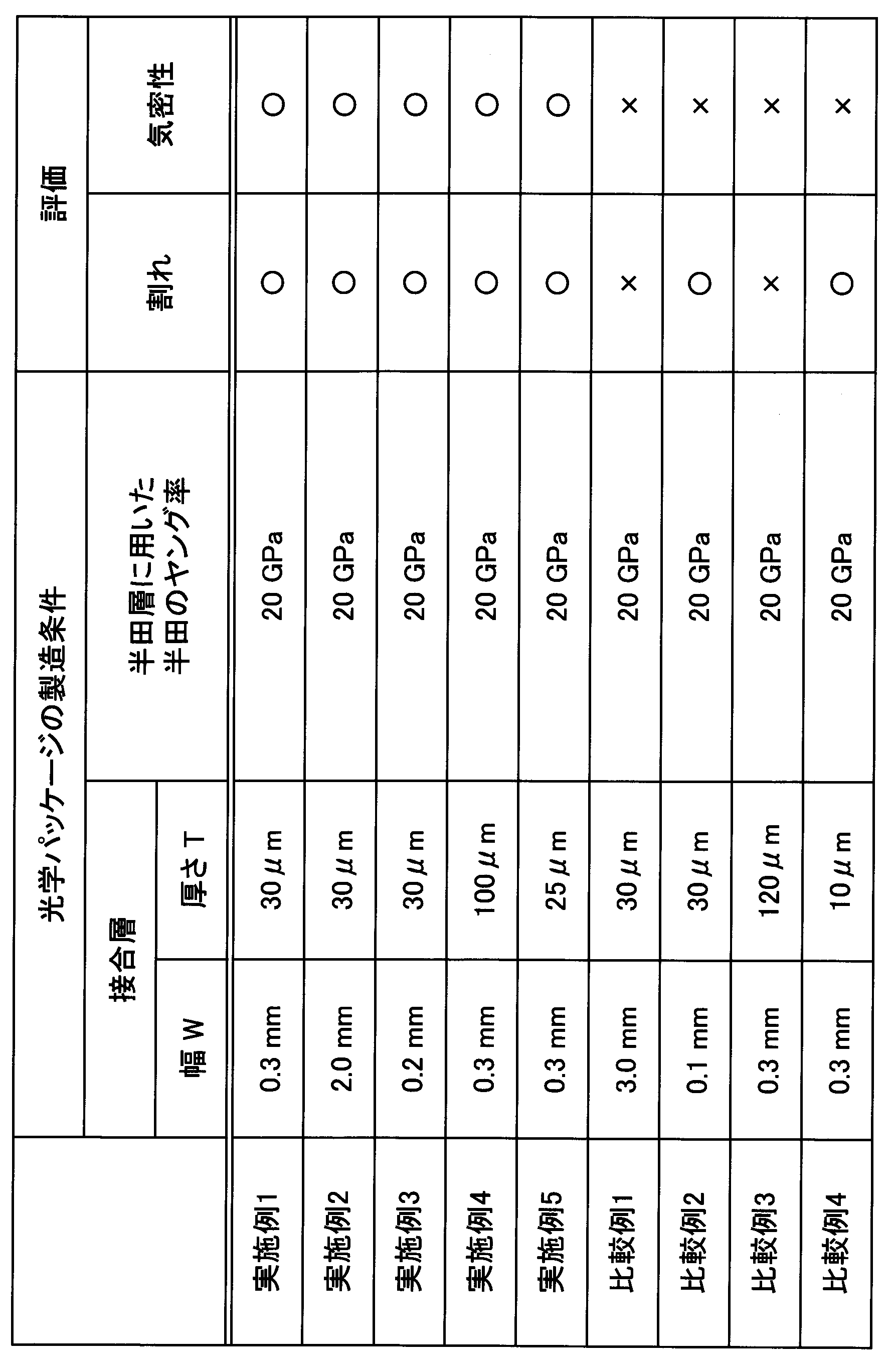
これに対して、接合層の幅、厚さが上記要件を充足しない比較例1~比較例4においては、割れが生じ、気密性が十分ではないことも確認できた。
以上に窓材、光学パッケージを、実施形態等で説明したが、本発明は上記実施形態等に限定されない。請求の範囲に記載された本発明の要旨の範囲内において、種々の変形、変更が可能である。
本出願は、2018年10月5日に日本国特許庁に出願された特願2018-190370号に基づく優先権を主張するものであり、特願2018-190370号の全内容を本国際出願に援用する。
10 窓材
11 無機材料の基体
12 接合層
122 半田層
30 光学パッケージ
31 回路基板
311 絶縁性基材
32 光学素子
11 無機材料の基体
12 接合層
122 半田層
30 光学パッケージ
31 回路基板
311 絶縁性基材
32 光学素子
Claims (6)
- 光学素子を備えた光学パッケージ用の窓材であって、
無機材料の基体と、
前記無機材料の基体の一方の面上に、前記無機材料の基体の外周に沿って配置された接合層とを有し、
前記接合層の幅が0.2mm以上2mm以下であり、
前記接合層の厚さが15μmより厚く100μm以下である窓材。 - 前記接合層は半田層を有しており、前記半田層に含まれる半田のヤング率Eが50GPa以下である請求項1に記載の窓材。
- 20℃以上200℃以下における、前記無機材料の基体の熱膨張係数と前記半田の熱膨張係数との差が30ppm/℃以下である請求項2に記載の窓材。
- 前記無機材料の基体と、前記接合層との界面における残留応力が100MPa以下である請求項1から請求項3のいずれか一項に記載の窓材。
- 請求項1から請求項4のいずれか一項に記載の窓材と、光学素子を備えた回路基板とを有する光学パッケージ。
- 前記回路基板はセラミックス製の絶縁性基材を有する請求項5に記載の光学パッケージ。
Priority Applications (4)
| Application Number | Priority Date | Filing Date | Title |
|---|---|---|---|
| JP2020550519A JP7435460B2 (ja) | 2018-10-05 | 2019-10-02 | 窓材、光学パッケージ |
| KR1020217008031A KR102656315B1 (ko) | 2018-10-05 | 2019-10-02 | 창재, 광학 패키지 |
| CN201980062389.3A CN112753100A (zh) | 2018-10-05 | 2019-10-02 | 窗材料、光学封装体 |
| JP2024015863A JP2024052748A (ja) | 2018-10-05 | 2024-02-05 | 窓材、光学パッケージ |
Applications Claiming Priority (2)
| Application Number | Priority Date | Filing Date | Title |
|---|---|---|---|
| JP2018-190370 | 2018-10-05 | ||
| JP2018190370 | 2018-10-05 |
Publications (1)
| Publication Number | Publication Date |
|---|---|
| WO2020071452A1 true WO2020071452A1 (ja) | 2020-04-09 |
Family
ID=70054683
Family Applications (1)
| Application Number | Title | Priority Date | Filing Date |
|---|---|---|---|
| PCT/JP2019/038997 Ceased WO2020071452A1 (ja) | 2018-10-05 | 2019-10-02 | 窓材、光学パッケージ |
Country Status (5)
| Country | Link |
|---|---|
| JP (2) | JP7435460B2 (ja) |
| KR (1) | KR102656315B1 (ja) |
| CN (1) | CN112753100A (ja) |
| TW (1) | TWI850267B (ja) |
| WO (1) | WO2020071452A1 (ja) |
Cited By (4)
| Publication number | Priority date | Publication date | Assignee | Title |
|---|---|---|---|---|
| WO2022004390A1 (ja) * | 2020-06-29 | 2022-01-06 | 日本電気硝子株式会社 | 蓋部材、蓋部材の製造方法、パッケージ、及びパッケージの製造方法 |
| WO2023067860A1 (ja) * | 2021-10-22 | 2023-04-27 | 日本電気硝子株式会社 | 保護キャップ、電子装置及び保護キャップの製造方法 |
| JP2024003052A (ja) * | 2020-10-28 | 2024-01-11 | 豊田合成株式会社 | 発光装置 |
| WO2024201707A1 (ja) * | 2023-03-28 | 2024-10-03 | 日本碍子株式会社 | 光学部品、透明封止部材、基板、及び光学部品の製造方法 |
Citations (5)
| Publication number | Priority date | Publication date | Assignee | Title |
|---|---|---|---|---|
| JP2002334943A (ja) * | 2001-05-09 | 2002-11-22 | Murata Mfg Co Ltd | 電子部品 |
| JP2004207539A (ja) * | 2002-12-26 | 2004-07-22 | Kyocera Corp | 電子部品収納用容器および電子装置 |
| JP2008118585A (ja) * | 2006-11-08 | 2008-05-22 | Nippon Dempa Kogyo Co Ltd | 表面実装用の電子部品 |
| JP2009200093A (ja) * | 2008-02-19 | 2009-09-03 | Murata Mfg Co Ltd | 中空型の電子部品 |
| JP2018037581A (ja) * | 2016-09-01 | 2018-03-08 | 日機装株式会社 | 光半導体装置および光半導体装置の製造方法 |
Family Cites Families (14)
| Publication number | Priority date | Publication date | Assignee | Title |
|---|---|---|---|---|
| JPS5877487U (ja) | 1981-11-20 | 1983-05-25 | リコーエレメックス株式会社 | 電子時計 |
| TW408495B (en) * | 1998-12-09 | 2000-10-11 | Shie Jeng Shiung | Vacuum package method of the infrared microsense device |
| JP2001071173A (ja) * | 1999-09-06 | 2001-03-21 | Ishikawa Kinzoku Kk | 無鉛はんだ |
| JP2004258269A (ja) * | 2003-02-25 | 2004-09-16 | Kyocera Corp | 光半導体素子収納用パッケージおよび光半導体装置 |
| JP3655916B2 (ja) * | 2003-04-04 | 2005-06-02 | 新光電気工業株式会社 | 半導体装置用キャップ |
| JP2006033265A (ja) * | 2004-07-14 | 2006-02-02 | Seiko Epson Corp | 圧電デバイスの製造方法 |
| JP2009212281A (ja) * | 2008-03-04 | 2009-09-17 | Panasonic Corp | 半導体発光装置 |
| JP5379403B2 (ja) * | 2008-05-12 | 2013-12-25 | 株式会社弘輝 | 鉛フリーSn−Ni系半田合金及び半田合金粉末 |
| US20100006108A1 (en) * | 2008-07-14 | 2010-01-14 | Sean Patrick Kerklaan | Anti-snore garment |
| WO2013005312A1 (ja) * | 2011-07-06 | 2013-01-10 | 有限会社ソフィアプロダクト | 酸化物接合材及びこれを用いた接合体 |
| JP2017001093A (ja) * | 2015-02-04 | 2017-01-05 | 日本電波工業株式会社 | はんだ材料及び電子部品 |
| JP6788337B2 (ja) * | 2015-10-16 | 2020-11-25 | Agc株式会社 | 接合用組成物 |
| JP6234488B2 (ja) * | 2016-02-05 | 2017-11-22 | 株式会社リソー技研 | 無鉛はんだ |
| US20190296194A1 (en) * | 2016-06-10 | 2019-09-26 | Nippon Electric Glass Co., Ltd. | Method for producing hermetic package, and hermetic package |
-
2019
- 2019-10-02 KR KR1020217008031A patent/KR102656315B1/ko active Active
- 2019-10-02 JP JP2020550519A patent/JP7435460B2/ja active Active
- 2019-10-02 CN CN201980062389.3A patent/CN112753100A/zh active Pending
- 2019-10-02 WO PCT/JP2019/038997 patent/WO2020071452A1/ja not_active Ceased
- 2019-10-03 TW TW108135875A patent/TWI850267B/zh active
-
2024
- 2024-02-05 JP JP2024015863A patent/JP2024052748A/ja active Pending
Patent Citations (5)
| Publication number | Priority date | Publication date | Assignee | Title |
|---|---|---|---|---|
| JP2002334943A (ja) * | 2001-05-09 | 2002-11-22 | Murata Mfg Co Ltd | 電子部品 |
| JP2004207539A (ja) * | 2002-12-26 | 2004-07-22 | Kyocera Corp | 電子部品収納用容器および電子装置 |
| JP2008118585A (ja) * | 2006-11-08 | 2008-05-22 | Nippon Dempa Kogyo Co Ltd | 表面実装用の電子部品 |
| JP2009200093A (ja) * | 2008-02-19 | 2009-09-03 | Murata Mfg Co Ltd | 中空型の電子部品 |
| JP2018037581A (ja) * | 2016-09-01 | 2018-03-08 | 日機装株式会社 | 光半導体装置および光半導体装置の製造方法 |
Cited By (13)
| Publication number | Priority date | Publication date | Assignee | Title |
|---|---|---|---|---|
| WO2022004390A1 (ja) * | 2020-06-29 | 2022-01-06 | 日本電気硝子株式会社 | 蓋部材、蓋部材の製造方法、パッケージ、及びパッケージの製造方法 |
| JP2024012427A (ja) * | 2020-10-28 | 2024-01-30 | 豊田合成株式会社 | 発光装置 |
| JP2024003052A (ja) * | 2020-10-28 | 2024-01-11 | 豊田合成株式会社 | 発光装置 |
| JP2024003051A (ja) * | 2020-10-28 | 2024-01-11 | 豊田合成株式会社 | 発光装置 |
| JP2024003050A (ja) * | 2020-10-28 | 2024-01-11 | 豊田合成株式会社 | 発光装置 |
| JP7533738B2 (ja) | 2020-10-28 | 2024-08-14 | 豊田合成株式会社 | 発光装置 |
| JP7533739B2 (ja) | 2020-10-28 | 2024-08-14 | 豊田合成株式会社 | 発光装置 |
| JP2023062928A (ja) * | 2021-10-22 | 2023-05-09 | 日本電気硝子株式会社 | 保護キャップ、電子装置及び保護キャップの製造方法 |
| WO2023067860A1 (ja) * | 2021-10-22 | 2023-04-27 | 日本電気硝子株式会社 | 保護キャップ、電子装置及び保護キャップの製造方法 |
| JP7627442B2 (ja) | 2021-10-22 | 2025-02-06 | 日本電気硝子株式会社 | 保護キャップ、電子装置及び保護キャップの製造方法 |
| KR102951646B1 (ko) | 2021-10-22 | 2026-04-13 | 니폰 덴키 가라스 가부시키가이샤 | 보호캡, 전자 장치 및 보호캡의 제조 방법 |
| WO2024201707A1 (ja) * | 2023-03-28 | 2024-10-03 | 日本碍子株式会社 | 光学部品、透明封止部材、基板、及び光学部品の製造方法 |
| WO2024204450A1 (ja) * | 2023-03-28 | 2024-10-03 | 日本碍子株式会社 | 光学部品、透明封止部材、基板、及び光学部品の製造方法 |
Also Published As
| Publication number | Publication date |
|---|---|
| CN112753100A (zh) | 2021-05-04 |
| KR20210070279A (ko) | 2021-06-14 |
| KR102656315B1 (ko) | 2024-04-09 |
| JPWO2020071452A1 (ja) | 2021-09-02 |
| TWI850267B (zh) | 2024-08-01 |
| JP2024052748A (ja) | 2024-04-12 |
| JP7435460B2 (ja) | 2024-02-21 |
| TW202029527A (zh) | 2020-08-01 |
Similar Documents
| Publication | Publication Date | Title |
|---|---|---|
| JP2024052748A (ja) | 窓材、光学パッケージ | |
| KR102563840B1 (ko) | 창재, 광학 패키지 | |
| TWI462236B (zh) | 副載置片及其製造方法 | |
| US20060198162A1 (en) | Light emitting element mounting member, and semiconductor device using the same | |
| KR102587868B1 (ko) | 패키지, 패키지 제조 방법, 접합재가 부착된 덮개체, 및 접합재가 부착된 덮개체의 제조 방법 | |
| JP2002359425A (ja) | サブマウントおよび半導体装置 | |
| WO2020022278A1 (ja) | 光学パッケージ | |
| WO2003069743A1 (en) | Sub-mount and semiconductor device | |
| JP2020065052A (ja) | パッケージ用蓋材及びパッケージ | |
| TWI884280B (zh) | 保護蓋、電子裝置及保護蓋的製造方法 | |
| CN114864785B (zh) | 封装用盖部件及封装体的制造方法 | |
| US20240429675A1 (en) | Film-equipped component and optical device | |
| JP7473877B2 (ja) | 蓋部材の製造方法 | |
| CN116438669A (zh) | 盖构件、封装体以及玻璃基板 | |
| JP7532979B2 (ja) | はんだ膜、光学デバイス用部品、及び光学デバイス | |
| HK40070310A (en) | Lid component for packages and package manufacturing method | |
| KR20200144144A (ko) | 패키지용 덮개재의 제조 방법 및 패키지의 제조 방법 | |
| WO2021014925A1 (ja) | 発光装置のリッド材およびリッド材の製造方法 | |
| JP2022021508A (ja) | はんだ膜、光学デバイス用部品、及び光学デバイス | |
| WO2021014904A1 (ja) | 発光装置のリッド材、リッド材の製造方法および発光装置 | |
| JP2010027434A (ja) | 蛍光表示装置 |
Legal Events
| Date | Code | Title | Description |
|---|---|---|---|
| 121 | Ep: the epo has been informed by wipo that ep was designated in this application |
Ref document number: 19868690 Country of ref document: EP Kind code of ref document: A1 |
|
| ENP | Entry into the national phase |
Ref document number: 2020550519 Country of ref document: JP Kind code of ref document: A |
|
| NENP | Non-entry into the national phase |
Ref country code: DE |
|
| 122 | Ep: pct application non-entry in european phase |
Ref document number: 19868690 Country of ref document: EP Kind code of ref document: A1 |