WO2020071391A1 - 半導体用接着剤、半導体装置の製造方法及び半導体装置 - Google Patents
半導体用接着剤、半導体装置の製造方法及び半導体装置Info
- Publication number
- WO2020071391A1 WO2020071391A1 PCT/JP2019/038821 JP2019038821W WO2020071391A1 WO 2020071391 A1 WO2020071391 A1 WO 2020071391A1 JP 2019038821 W JP2019038821 W JP 2019038821W WO 2020071391 A1 WO2020071391 A1 WO 2020071391A1
- Authority
- WO
- WIPO (PCT)
- Prior art keywords
- semiconductor
- adhesive
- resin
- semiconductor device
- semiconductor chip
- Prior art date
- Legal status (The legal status is an assumption and is not a legal conclusion. Google has not performed a legal analysis and makes no representation as to the accuracy of the status listed.)
- Ceased
Links
Images


Classifications
-
- C—CHEMISTRY; METALLURGY
- C09—DYES; PAINTS; POLISHES; NATURAL RESINS; ADHESIVES; COMPOSITIONS NOT OTHERWISE PROVIDED FOR; APPLICATIONS OF MATERIALS NOT OTHERWISE PROVIDED FOR
- C09J—ADHESIVES; NON-MECHANICAL ASPECTS OF ADHESIVE PROCESSES IN GENERAL; ADHESIVE PROCESSES NOT PROVIDED FOR ELSEWHERE; USE OF MATERIALS AS ADHESIVES
- C09J11/00—Features of adhesives not provided for in group C09J9/00, e.g. additives
- C09J11/02—Non-macromolecular additives
- C09J11/04—Non-macromolecular additives inorganic
-
- C—CHEMISTRY; METALLURGY
- C09—DYES; PAINTS; POLISHES; NATURAL RESINS; ADHESIVES; COMPOSITIONS NOT OTHERWISE PROVIDED FOR; APPLICATIONS OF MATERIALS NOT OTHERWISE PROVIDED FOR
- C09J—ADHESIVES; NON-MECHANICAL ASPECTS OF ADHESIVE PROCESSES IN GENERAL; ADHESIVE PROCESSES NOT PROVIDED FOR ELSEWHERE; USE OF MATERIALS AS ADHESIVES
- C09J11/00—Features of adhesives not provided for in group C09J9/00, e.g. additives
- C09J11/02—Non-macromolecular additives
- C09J11/06—Non-macromolecular additives organic
-
- C—CHEMISTRY; METALLURGY
- C09—DYES; PAINTS; POLISHES; NATURAL RESINS; ADHESIVES; COMPOSITIONS NOT OTHERWISE PROVIDED FOR; APPLICATIONS OF MATERIALS NOT OTHERWISE PROVIDED FOR
- C09J—ADHESIVES; NON-MECHANICAL ASPECTS OF ADHESIVE PROCESSES IN GENERAL; ADHESIVE PROCESSES NOT PROVIDED FOR ELSEWHERE; USE OF MATERIALS AS ADHESIVES
- C09J163/00—Adhesives based on epoxy resins; Adhesives based on derivatives of epoxy resins
-
- C—CHEMISTRY; METALLURGY
- C09—DYES; PAINTS; POLISHES; NATURAL RESINS; ADHESIVES; COMPOSITIONS NOT OTHERWISE PROVIDED FOR; APPLICATIONS OF MATERIALS NOT OTHERWISE PROVIDED FOR
- C09J—ADHESIVES; NON-MECHANICAL ASPECTS OF ADHESIVE PROCESSES IN GENERAL; ADHESIVE PROCESSES NOT PROVIDED FOR ELSEWHERE; USE OF MATERIALS AS ADHESIVES
- C09J7/00—Adhesives in the form of films or foils
- C09J7/30—Adhesives in the form of films or foils characterised by the adhesive composition
- C09J7/38—Pressure-sensitive adhesives [PSA]
-
- H—ELECTRICITY
- H10—SEMICONDUCTOR DEVICES; ELECTRIC SOLID-STATE DEVICES NOT OTHERWISE PROVIDED FOR
- H10W—GENERIC PACKAGES, INTERCONNECTIONS, CONNECTORS OR OTHER CONSTRUCTIONAL DETAILS OF DEVICES COVERED BY CLASS H10
- H10W74/00—Encapsulations, e.g. protective coatings
- H10W74/10—Encapsulations, e.g. protective coatings characterised by their shape or disposition
-
- H—ELECTRICITY
- H10—SEMICONDUCTOR DEVICES; ELECTRIC SOLID-STATE DEVICES NOT OTHERWISE PROVIDED FOR
- H10W—GENERIC PACKAGES, INTERCONNECTIONS, CONNECTORS OR OTHER CONSTRUCTIONAL DETAILS OF DEVICES COVERED BY CLASS H10
- H10W74/00—Encapsulations, e.g. protective coatings
- H10W74/10—Encapsulations, e.g. protective coatings characterised by their shape or disposition
- H10W74/111—Encapsulations, e.g. protective coatings characterised by their shape or disposition the semiconductor body being completely enclosed
- H10W74/127—Encapsulations, e.g. protective coatings characterised by their shape or disposition the semiconductor body being completely enclosed characterised by arrangements for sealing or adhesion
-
- H—ELECTRICITY
- H10—SEMICONDUCTOR DEVICES; ELECTRIC SOLID-STATE DEVICES NOT OTHERWISE PROVIDED FOR
- H10W—GENERIC PACKAGES, INTERCONNECTIONS, CONNECTORS OR OTHER CONSTRUCTIONAL DETAILS OF DEVICES COVERED BY CLASS H10
- H10W74/00—Encapsulations, e.g. protective coatings
- H10W74/40—Encapsulations, e.g. protective coatings characterised by their materials
-
- C—CHEMISTRY; METALLURGY
- C09—DYES; PAINTS; POLISHES; NATURAL RESINS; ADHESIVES; COMPOSITIONS NOT OTHERWISE PROVIDED FOR; APPLICATIONS OF MATERIALS NOT OTHERWISE PROVIDED FOR
- C09J—ADHESIVES; NON-MECHANICAL ASPECTS OF ADHESIVE PROCESSES IN GENERAL; ADHESIVE PROCESSES NOT PROVIDED FOR ELSEWHERE; USE OF MATERIALS AS ADHESIVES
- C09J2203/00—Applications of adhesives in processes or use of adhesives in the form of films or foils
- C09J2203/326—Applications of adhesives in processes or use of adhesives in the form of films or foils for bonding electronic components such as wafers, chips or semiconductors
-
- H—ELECTRICITY
- H10—SEMICONDUCTOR DEVICES; ELECTRIC SOLID-STATE DEVICES NOT OTHERWISE PROVIDED FOR
- H10W—GENERIC PACKAGES, INTERCONNECTIONS, CONNECTORS OR OTHER CONSTRUCTIONAL DETAILS OF DEVICES COVERED BY CLASS H10
- H10W90/00—Package configurations
- H10W90/701—Package configurations characterised by the relative positions of pads or connectors relative to package parts
- H10W90/721—Package configurations characterised by the relative positions of pads or connectors relative to package parts of bump connectors
- H10W90/726—Package configurations characterised by the relative positions of pads or connectors relative to package parts of bump connectors between a chip and a stacked lead frame, conducting package substrate or heat sink
Definitions
- the present disclosure relates to a semiconductor adhesive, a method for manufacturing a semiconductor device, and a semiconductor device.
- connection method FC connection method
- FC connection method a method of bonding a connection to a metal using solder, tin, gold, silver, copper, etc., a method of bonding a connection to a metal by applying ultrasonic vibration, and a mechanical contact by a contraction force of a resin are known. From the viewpoint of the reliability of the connection portion, a method of metal-joining the connection portion using solder, tin, gold, silver, copper, or the like is generally used.
- a COB (Chip On Board) type connection system which is frequently used in BGA (Ball Grid Array), CSP (Chip Size Package) and the like also corresponds to the FC connection system.
- a connection section (bump or wiring) is formed on a semiconductor chip to connect between semiconductor chips, and a connection section (bump or wiring) is formed on a semiconductor wafer.
- COW Chip ⁇ On ⁇ Wafer
- chip stack type packages in which the above-described connection methods are stacked and multi-staged, POP (Package On Package), TSV (Through-Silicon Via), and the like.
- POP Package On Package
- TSV Through-Silicon Via
- chip stack type packages in which the above-described connection methods are stacked and multi-staged, POP (Package On Package), TSV (Through-Silicon Via), and the like.
- POP Package On Package
- TSV Through-Silicon Via
- Such a stacking / multi-stage technique since semiconductor chips and the like are arranged three-dimensionally, the size of the package can be reduced as compared with a technique of arranging two-dimensionally.
- such a stacking / multi-stage technology is effective in improving the performance of semiconductors, reducing noise, reducing the mounting area, and saving power, and thus has attracted attention as a next-generation semiconductor wiring technology.
- Flip-chip packages which are becoming more sophisticated, highly integrated, and cost-effective, are expected to expand their applications and production volume in the future. Sustained mass production of flip-chip packages requires the continuous supply of semiconductor adhesives used for them. For this reason, semiconductor adhesives must have excellent stability over time. I have. If the stability over time of the adhesive for semiconductors is poor, the viscosity of the adhesive for semiconductors increases while being left at room temperature, and there is a concern that the mountability at the time of assembling the semiconductor device may deteriorate.
- the present disclosure is capable of suppressing an increase in viscosity after being left at room temperature, and is unlikely to cause deterioration in mountability when assembling a semiconductor device over time, and a method of manufacturing a semiconductor device using the same. It is an object to provide a semiconductor device.
- the present disclosure provides (a) an inorganic filler, wherein the (a) inorganic filler is a surface-treated inorganic filler having a glycidyl group, and the (a) inorganic filler as a whole. And a semiconductor adhesive containing 50% by mass or more based on the above. According to the adhesive for semiconductors described above, (a) 50% by mass or more of the entire inorganic filler is a surface-treated inorganic filler having a glycidyl group. An increase in viscosity can be suppressed.
- the surface treatment agent and moisture easily form a hydrogen bond to increase the viscosity, but the surface treatment having a glycidyl group is difficult.
- the surface treatment having a glycidyl group is difficult.
- the semiconductor adhesive an increase in viscosity after standing at room temperature can be suppressed, so that it is possible to suppress the deterioration of the mountability when assembling the semiconductor device over time.
- the inorganic filler is subjected to a surface treatment having a glycidyl group, the inorganic filler has excellent dispersibility in the adhesive for semiconductors, and the adhesive for semiconductors can obtain good adhesive strength and good insulation reliability. it can.
- the semiconductor adhesive may further contain (b) an epoxy resin, (c) a curing agent, and (d) a high molecular weight component having a weight average molecular weight of 10,000 or more. Further, the semiconductor adhesive may further contain (e) a flux agent.
- the semiconductor adhesive may be in the form of a film.
- the handleability of the semiconductor adhesive can be improved, and the workability and productivity during package manufacturing can be improved.
- the present disclosure also provides a method of manufacturing a semiconductor device in which connection portions of a semiconductor chip and a printed circuit board are electrically connected to each other, or a semiconductor device in which connection portions of a plurality of semiconductor chips are electrically connected to each other.
- a method for manufacturing a semiconductor device comprising: a step of sealing at least a part of the connection portion with the semiconductor adhesive. According to the above-mentioned manufacturing method, since the adhesive for semiconductor used is hard to increase in viscosity with time, good mounting performance can be obtained stably.
- the present disclosure further includes a connection structure in which connection portions of the semiconductor chip and the wiring circuit board are electrically connected to each other, or a connection structure in which connection portions of a plurality of semiconductor chips are electrically connected to each other, An adhesive material for sealing at least a part of the connection portion, wherein the adhesive material is made of a cured product of the semiconductor adhesive.
- the above-described semiconductor device has good mountability, and has excellent adhesion and reliability between the semiconductor chip and the printed circuit board or the semiconductor chip.
- the adhesive agent for semiconductors which can suppress the viscosity increase after leaving room temperature, and which hardly causes the deterioration of mountability at the time of assembling a semiconductor device over time, a method of manufacturing a semiconductor device using the same, and A semiconductor device can be provided.
- FIG. 1 is a schematic cross-sectional view illustrating an embodiment of a semiconductor device according to the present disclosure.
- FIG. 4 is a schematic cross-sectional view illustrating another embodiment of the semiconductor device of the present disclosure.
- FIG. 4 is a schematic cross-sectional view illustrating another embodiment of the semiconductor device of the present disclosure.
- FIG. 4 is a schematic cross-sectional view illustrating another embodiment of the semiconductor device of the present disclosure.
- a numerical range indicated by using “to” indicates a range including numerical values described before and after “to” as a minimum value and a maximum value, respectively.
- the upper limit or the lower limit of a numerical range in one step can be arbitrarily combined with the upper limit or the lower limit of a numerical range in another step.
- the upper limit or the lower limit of the numerical range may be replaced with the value shown in the embodiment.
- “A or B” may include one of A and B, and may include both.
- the materials exemplified in the present specification can be used alone or in combination of two or more, unless otherwise specified.
- “(meth) acryl” means acryl or methacryl corresponding thereto.
- the semiconductor adhesive according to the present embodiment contains (a) an inorganic filler (hereinafter sometimes referred to as “component (a)”).
- component (a) inorganic filler contains 50% by mass or more of an inorganic filler having a glycidyl group and subjected to a surface treatment, based on the total amount of the (a) inorganic filler.
- the semiconductor adhesive according to the present embodiment includes (b) an epoxy resin (hereinafter, sometimes referred to as “component (b)”) and (c) a curing agent (hereinafter, sometimes referred to as “component (c)”).
- the semiconductor adhesive according to the present embodiment may contain (e) a fluxing agent (hereinafter, sometimes referred to as “component (e)”).
- component (e) a fluxing agent
- the inorganic filler as the component (a) include an insulating inorganic filler. Among them, an inorganic filler having an average particle diameter of 100 nm or less is more preferable.
- the material of the insulating inorganic filler include glass, silica, alumina, silica / alumina, titanium oxide, mica, and boron nitride, among which silica, alumina, silica / alumina, titanium oxide, and boron nitride are preferable. Silica, alumina and boron nitride are more preferred.
- the insulating inorganic filler may be a whisker, and examples of the material of the whisker include aluminum borate, aluminum titanate, zinc oxide, calcium silicate, magnesium sulfate, and boron nitride.
- the insulating inorganic filler can be used alone or in combination of two or more.
- the component (a) is preferably a surface-treated filler.
- the surface treatment include glycidyl (epoxy), amine, phenyl, phenylamino, acryl, vinyl, and the like.
- a silane treatment with a silane compound such as an epoxy silane type, an amino silane type or an acryl silane type is preferable from the viewpoint of easy surface treatment.
- a silane compound such as an epoxy silane type, an amino silane type or an acryl silane type
- the surface treatment agent glycidyl-based, phenylamino-based, and (meth) acryl-based compounds are preferable from the viewpoint of excellent dispersibility and fluidity and further improving the adhesive strength.
- a glycidyl-based compound is preferable from the viewpoint of suppressing an increase in the viscosity of the semiconductor adhesive after standing at room temperature.
- the component (a) contains 50% by mass or more of a surface-treated inorganic filler having a glycidyl group, based on the total amount of the component (a).
- the surface treatment having a glycidyl group can be performed using a glycidyl-based compound having a structure represented by the following general formula (1) as a surface treatment agent.
- the surface of the inorganic filler has a structure represented by the following general formula (1).
- R represents a divalent organic group.
- the content of the inorganic filler subjected to the surface treatment having a glycidyl group is 50% by mass or more based on the total amount of the component (a), and from the viewpoint of further suppressing the increase in the viscosity of the semiconductor adhesive after standing at room temperature, It is preferably at least 60% by mass, more preferably at least 80% by mass.
- the entire amount (100% by mass) of the component (a) may be a surface-treated inorganic filler having a glycidyl group.
- the average particle diameter of the component (a) is preferably 100 nm or less, and more preferably 60 nm or less.
- the average particle size of the component (a) can be measured by a laser diffraction type particle size distribution meter.
- the viscosity of the semiconductor adhesive may become too low due to the large particle size, and the semiconductor adhesive may be mounted outside a chip called a fillet after mounting. Of the resin may easily occur.
- the viscosity of the semiconductor adhesive is easily adjusted to a preferable range, and the generation of fillets is sufficiently suppressed, or the amount of fillets is sufficiently reduced. can do.
- the lower limit of the average particle diameter of the component (a) is not particularly limited, but may be 1 nm or more, 5 nm or more, or 10 nm or more from the viewpoint of suppressing aggregation of the component (a).
- aggregation may occur even if the average particle size is about 50 nm, but an inorganic filler that has been subjected to a surface treatment having a glycidyl group is used. In this case, even if the average particle size is about 50 nm or less, the occurrence of aggregation can be suppressed.
- the component (a) can be used alone or as a mixture of two or more.
- the shape of the component (a) is not particularly limited.
- the content of the component (a) is preferably from 10 to 80% by mass, more preferably from 15 to 60% by mass, and more preferably from 20 to 50% by mass, based on the total solid content of the semiconductor adhesive. It is even more preferred. When the content is 10% by mass or more, the adhesive strength and the reflow resistance tend to be further improved. When the content is 80% by mass or less, the decrease in connection reliability due to thickening tends to be suppressed. .
- the semiconductor adhesive according to the present embodiment may contain a resin filler.
- the resin filler include a filler made of a resin such as polyurethane and polyimide.
- the resin filler has a smaller coefficient of thermal expansion than other organic components (such as an epoxy resin and a curing agent), and thus has an excellent effect of improving connection reliability. Further, according to the resin filler, the viscosity of the semiconductor adhesive can be easily adjusted. Further, the resin filler has an excellent function of relieving stress as compared with the inorganic filler.
- the filler contained in the semiconductor adhesive is preferably insulating. It is preferable that the semiconductor adhesive does not contain a conductive metal filler such as a silver filler and a solder filler.
- An adhesive for semiconductors (circuit connecting material) that does not contain conductive fillers (conductive particles) is sometimes called NCF (Non-Conductive-FILM) or NCP (Non-Conductive-Paste).
- the semiconductor adhesive according to the present embodiment can be suitably used as NCF or NCP.
- the epoxy resin (b) include an epoxy resin having two or more epoxy groups in a molecule, such as a bisphenol A epoxy resin, a bisphenol F epoxy resin, a naphthalene epoxy resin, a phenol novolak epoxy resin, Cresol novolak type epoxy resin, phenol aralkyl type epoxy resin, biphenyl type epoxy resin, triphenylmethane type epoxy resin, dicyclopentadiene type epoxy resin, various polyfunctional epoxy resins and the like can be used.
- the component (b) one type can be used alone, or two or more types can be used in combination.
- the bisphenol A type or the bisphenol F type liquid epoxy resin has a 1% thermal weight loss temperature of 250 ° C. or less, and thus may be decomposed when heated at a high temperature to generate volatile components. Therefore, it is preferable to use an epoxy resin that is solid at room temperature (1 atm, 25 ° C.). When using a liquid epoxy resin, it is preferable to use it in combination with a solid epoxy resin.
- the weight average molecular weight of the component (b) may be less than 10,000, and from the viewpoint of heat resistance, is preferably 100 or more and less than 10,000, more preferably 300 or more and 8000 or less, and further preferably 300 or more and 5000 or less.
- the content of the component (b) is preferably from 10 to 50% by mass, more preferably from 20 to 45% by mass, and still more preferably from 30 to 40% by mass, based on the total solid content of the semiconductor adhesive. It is. When the content of the component (b) is 10% by mass or more, it is easy to sufficiently control the flow of the cured resin. When the content is 50% by mass or less, the resin component of the cured product does not become too large, and Easy to reduce warpage.
- the semiconductor adhesive according to the present embodiment may further contain a thermosetting resin other than the epoxy resin (b).
- thermosetting resins include phenolic resins, imide resins, (meth) acrylic compounds, and the like.
- Component (c): curing agent examples include a phenol resin-based curing agent, an acid anhydride-based curing agent, an amine-based curing agent, an imidazole-based curing agent, and a phosphine-based curing agent.
- the component (c) contains a phenolic hydroxyl group, an acid anhydride, an amine or an imidazole, it is easy to exhibit a flux activity for suppressing the formation of an oxide film at the connection portion, thereby easily improving connection reliability and insulation reliability. Can be done.
- each curing agent will be described.
- Phenolic resin-based curing agent examples include curing agents having two or more phenolic hydroxyl groups in a molecule, such as phenol novolak resin, cresol novolak resin, phenol aralkyl resin, and cresol naphthol. Formaldehyde polycondensates, triphenylmethane-type polyfunctional phenol resins, various polyfunctional phenol resins, and the like can be used.
- the phenolic resin-based curing agents can be used alone or in combination of two or more.
- the equivalent ratio of the phenolic resin-based curing agent to the component (b) is preferably from 0.3 to 1.5 from the viewpoint of excellent curability, adhesiveness and storage stability. , 0.4 to 1.0, more preferably 0.5 to 1.0.
- the equivalent ratio is 0.3 or more, the curability tends to be improved and the adhesive strength tends to be improved.
- the equivalent ratio is 1.5 or less, unreacted phenolic hydroxyl groups do not remain excessively, and the water absorption Is kept low, and the insulation reliability tends to be further improved.
- Acid anhydride-based curing agent examples include methylcyclohexanetetracarboxylic dianhydride, trimellitic anhydride, pyromellitic anhydride, benzophenonetetracarboxylic dianhydride, and ethylene glycol bis. Anhydrotrimellitate or the like can be used.
- the acid anhydride-based curing agent can be used alone or in combination of two or more.
- the equivalent ratio of the acid anhydride-based curing agent to the component (b) is from 0.3 to 1.5 from the viewpoint of excellent curability, adhesiveness and storage stability. Is preferably, 0.4 to 1.0 is more preferable, and 0.5 to 1.0 is more preferable. When the equivalent ratio is 0.3 or more, the curability tends to be improved and the adhesive strength tends to be improved. When the equivalent ratio is 1.5 or less, the unreacted acid anhydride does not remain excessively, and the water absorption Is kept low, and the insulation reliability tends to be further improved.
- (C-iii) Amine-based curing agent As the amine-based curing agent, dicyandiamide, various amine compounds, and the like can be used.
- the equivalent ratio of the amine-based curing agent to the component (b) is preferably from 0.3 to 1.5 from the viewpoint of excellent curability, adhesion and storage stability. -1.0 is more preferable, and 0.5-1.0 is more preferable. When the equivalent ratio is 0.3 or more, the curability tends to be improved and the adhesive strength tends to be improved. When the equivalent ratio is 1.5 or less, unreacted amine does not remain excessively, and insulation reliability is improved. There is a tendency to further improve.
- imidazole curing agent examples include 2-phenylimidazole, 2-phenyl-4-methylimidazole, 1-benzyl-2-methylimidazole, 1-benzyl-2-phenylimidazole, Cyanoethyl-2-undecylimidazole, 1-cyano-2-phenylimidazole, 1-cyanoethyl-2-undecylimidazole trimellitate, 1-cyanoethyl-2-phenylimidazolium trimellitate, 2,4-diamino-6 -[2′-methylimidazolyl- (1 ′)]-ethyl-s-triazine, 2,4-diamino-6- [2′-undecylimidazolyl- (1 ′)]-ethyl-s-triazine, 2, 4-diamino-6- [2'-ethyl-4'-methylimidazolyl
- 1-cyanoethyl-2-undecylimidazole, 1-cyano-2-phenylimidazole, 1-cyanoethyl-2-undecylimidazole trimellit from the viewpoint of further improving curability, storage stability and connection reliability.
- the content of the imidazole-based curing agent is preferably from 0.1 to 20 parts by mass, more preferably from 0.1 to 10 parts by mass, per 100 parts by mass of the component (b).
- the content of the imidazole-based curing agent is 0.1 part by mass or more, the curability tends to be improved, and when the content is 20 parts by mass or less, the adhesive composition is cured before metal bonding is formed. And there is a tendency that poor connection hardly occurs.
- (Cv) Phosphine-based curing agent examples include triphenylphosphine, tetraphenylphosphonium tetraphenylborate, tetraphenylphosphonium tetra (4-methylphenyl) borate, and tetraphenylphosphonium (4-fluorophenyl) borate. Is mentioned.
- the content of the phosphine-based curing agent is preferably from 0.1 to 10 parts by mass, more preferably from 0.1 to 5 parts by mass, per 100 parts by mass of the component (b).
- the content of the phosphine-based curing agent is 0.1 part by mass or more, the curability tends to be improved, and when the content is 10 parts by mass or less, the semiconductor adhesive is cured before metal bonding is formed. And there is a tendency that poor connection hardly occurs.
- the phenolic resin-based curing agent, acid anhydride-based curing agent, and amine-based curing agent can be used alone or in combination of two or more.
- the imidazole-based curing agent and the phosphine-based curing agent may be used alone, but may be used together with a phenolic resin-based curing agent, an acid anhydride-based curing agent, or an amine-based curing agent.
- the component (c) from the viewpoint of excellent curability, a combined use of a phenolic resin-based curing agent and an imidazole-based curing agent, a combined use of an acid anhydride-based curing agent and an imidazole-based curing agent, an amine-based curing agent and an imidazole-based curing agent And the use of an imidazole-based curing agent alone is preferred. Since the productivity is improved when the connection is made in a short time, it is more preferable to use an imidazole-based curing agent having excellent quick-curing properties alone. In this case, when cured in a short time, volatile components such as low molecular components can be suppressed, so that the generation of voids can be easily suppressed.
- the high molecular weight component having a weight average molecular weight of 10,000 or more includes phenoxy resin, polyimide resin, polyamide resin, polycarbodiimide resin, cyanate ester resin, (meth) acrylic resin, Polyester resin, polyethylene resin, polyether sulfone resin, polyetherimide resin, polyvinyl acetal resin, polyurethane resin, acrylic rubber, and the like, among which, from the viewpoint of excellent heat resistance and film formability, phenoxy resin, polyimide resin, (Meth) acrylic resin, acrylic rubber, cyanate ester resin and polycarbodiimide resin are preferred, phenoxy resin, polyimide resin, (meth) acrylic resin and acrylic rubber are more preferred, and phenoxy resin is even more preferred.
- the component (d) may be used alone or as a mixture or copolymer of two or more.
- the mass ratio of the component (d) to the component (b) is not particularly limited, but from the viewpoint of maintaining a good film shape, the content of the component (b) is 1 part by mass of the component (d).
- the amount is preferably 0.01 to 5 parts by mass, more preferably 0.05 to 4 parts by mass, and even more preferably 0.1 to 3 parts by mass.
- the content of the component (b) is 0.01 parts by mass or more, the curability does not decrease, and the adhesive strength does not decrease.
- the content is 5 parts by mass or less, the film formability and the film are reduced. The formability does not decrease.
- the weight average molecular weight of the component (d) is 10,000 or more in terms of polystyrene, but is preferably 30,000 or more, more preferably 40,000 or more, and still more preferably 50,000 or more, in order to show good film-forming properties by itself.
- the weight average molecular weight is 10,000 or more, there is no possibility that the film forming property is reduced.
- the weight-average molecular weight means a weight-average molecular weight measured by high-performance liquid chromatography (Shimadzu Corporation, CR4A) in terms of polystyrene.
- the semiconductor adhesive may further contain (e) a flux agent which is a compound exhibiting flux activity (activity for removing oxides, impurities, and the like).
- a flux agent which is a compound exhibiting flux activity (activity for removing oxides, impurities, and the like).
- the flux agent include nitrogen-containing compounds having an unshared electron pair (imidazoles, amines, etc., except those contained in the component (c)), carboxylic acids, phenols, alcohols, and the like. Note that carboxylic acids exhibit stronger flux activity than alcohols, and are more likely to improve connectivity.
- the content of the component (e) is preferably from 0.2 to 3% by mass, and more preferably from 0.4 to 1.8% by mass, based on the total solid content of the semiconductor adhesive. Is more preferable.
- the semiconductor adhesive may further contain an ion trapper, an antioxidant, a silane coupling agent, a titanium coupling agent, a leveling agent, and the like. These may be used alone or in combination of two or more. What is necessary is just to adjust suitably these compounding quantities so that the effect of each additive may be exhibited.
- the shear viscosity at 80 ° C. when the semiconductor adhesive is formed into a film is preferably 4500 to 14000 Pa ⁇ s, more preferably 5000 to 13000 Pa ⁇ s, and more preferably 5000 to 10000 Pa ⁇ s. More preferred.
- the shear viscosity is 4500 Pa ⁇ s or more, generation of fillets can be sufficiently suppressed, or the amount of fillets can be sufficiently reduced.
- the shear viscosity is 14000 Pa ⁇ s or less, the mountability at the time of assembling the semiconductor device can be improved.
- the shear viscosity of the film-form semiconductor adhesive can be measured, for example, by using a dynamic shear viscoelasticity measuring device (trade name “ARES-G2” manufactured by TA Instruments Japan Co., Ltd.). It can be measured under the conditions of 10 ° C./min, a measurement temperature range of 30 ° C. to 145 ° C., and a frequency of 10 Hz.
- the value of the viscosity at 80 ° C. of the viscosity value measured by the above method can be determined as the shear viscosity at 80 ° C. when the adhesive for a semiconductor is formed into a film.
- the adhesive for semiconductors according to the present embodiment is preferably in the form of a film (film-like adhesive) from the viewpoint of improving productivity.
- the method for producing the film adhesive will be described below.
- component, (b) component, (c) component, (d) component, and other components as necessary are added to an organic solvent, and then dissolved or dispersed by stirring, mixing, kneading, or the like.
- the organic solvent is reduced by heating, and the base film is removed.
- a film adhesive may be formed on the wafer by a method of spin-coating a resin varnish on a wafer or the like to form a film, and then drying the solvent.
- organic solvent used for preparing the resin varnish those having properties capable of uniformly dissolving or dispersing each component are preferable, for example, dimethylformamide, dimethylacetamide, N-methyl-2-pyrrolidone, dimethylsulfoxide, diethylene glycol dimethyl ether, Examples include toluene, benzene, xylene, methyl ethyl ketone, tetrahydrofuran, ethyl cellosolve, ethyl cellosolve acetate, butyl cellosolve, dioxane, cyclohexanone, and ethyl acetate. These organic solvents can be used alone or in combination of two or more.
- the stirring, mixing and kneading at the time of preparing the resin varnish can be performed using, for example, a stirrer, a raker, a three-roll, a ball mill, a bead mill or a homodisper.
- the substrate film is not particularly limited as long as it has heat resistance enough to withstand the heating conditions when the organic solvent is volatilized, and polyester film, polypropylene film, polyethylene terephthalate film, polyimide film, polyetherimide film, polyether Ether naphthalate film, methylpentene film and the like can be mentioned.
- the base film is not limited to a single layer made of one of these films, and may be a multilayer film made of two or more films.
- the thickness of the film in the film adhesive according to the present embodiment is preferably from 10 to 100 ⁇ m, and more preferably from 20 to 50 ⁇ m, from the viewpoint of visibility, fluidity, and filling property.
- the semiconductor adhesive according to the present embodiment is preferably used for a semiconductor device, and a semiconductor device in which electrodes of respective connection portions of a semiconductor chip and a wiring circuit board are electrically connected to each other, or a plurality of semiconductor chips.
- a semiconductor device in which electrodes of respective connection portions are electrically connected to each other it is particularly suitably used for sealing the connection portions.
- the electrodes of the connection portion in the semiconductor device may be either a metal joint between the bump and the wiring or a metal joint between the bump and the bump.
- flip-chip connection for obtaining electrical connection via a semiconductor adhesive may be used.
- FIG. 1 is a schematic cross-sectional view showing an embodiment of a semiconductor device (COB-type connection between a semiconductor chip and a substrate).
- the first semiconductor device 100 is arranged on a semiconductor chip 10 and a substrate (wiring circuit board) 20 facing each other, and on a surface of the semiconductor chip 10 and the substrate 20 facing each other.
- the semiconductor chip 10 and the substrate 20 are flip-chip connected by the wiring 15 and the connection bump 30.
- the wiring 15 and the connection bump 30 are sealed with an adhesive material 40 and are shielded from an external environment.
- the adhesive material 40 is a cured product of the semiconductor adhesive of the present embodiment.
- the second semiconductor device 200 is disposed on the semiconductor chip 10 and the substrate (wiring circuit substrate) 20 facing each other, and on the surfaces of the semiconductor chip 10 and the substrate 20 facing each other. And a bonding material 40 that fills the gap between the semiconductor chip 10 and the substrate 20 without any gap.
- the semiconductor chip 10 and the substrate 20 are flip-chip connected by connecting the opposing bumps 32 to each other.
- the bump 32 is sealed with an adhesive material 40 and is shielded from an external environment.
- FIG. 2 is a schematic sectional view showing another embodiment of the semiconductor device (COC type connection between semiconductor chips).
- the third semiconductor device 300 is the same as the first semiconductor device 100 except that two semiconductor chips 10 are flip-chip connected by wirings 15 and connection bumps 30. It is.
- the fourth semiconductor device 400 is similar to the second semiconductor device 200 except that two semiconductor chips 10 are flip-chip connected by bumps 32.
- the semiconductor chip 10 is not particularly limited, and various semiconductors such as element semiconductors composed of the same kind of elements such as silicon and germanium, and compound semiconductors such as gallium / arsenic and indium / phosphorus can be used.
- the substrate 20 is not particularly limited as long as it is a printed circuit board, and is formed on the surface of an insulating substrate mainly composed of glass epoxy resin, polyimide resin, polyester resin, ceramic, epoxy resin, bismaleimide triazine resin and the like.
- a circuit board or the like on which a conductive material is printed to form a wiring (wiring pattern) can be used.
- Connections such as the wiring 15 and the bumps 32 are mainly composed of gold, silver, copper, solder (for example, tin-silver, tin-lead, tin-bismuth, tin-copper), nickel, tin, lead, etc. And may contain a plurality of metals.
- a metal layer may be formed. This metal layer may be composed of only a single component, or may be composed of a plurality of components. Further, a structure in which a plurality of metal layers are stacked may be employed. Copper and solder are generally used because they are inexpensive. Since copper and solder contain oxides and impurities, the semiconductor adhesive preferably has flux activity.
- the material of the conductive protrusions called bumps is mainly composed of gold, silver, copper, solder (for example, tin-silver, tin-lead, tin-bismuth, tin-copper), tin, nickel, etc. And may be composed of only a single component, or may be composed of a plurality of components. Further, these metals may be formed so as to form a laminated structure.
- the bump may be formed on a semiconductor chip or a substrate. Copper and solder are generally used because they are inexpensive. Since copper and solder contain oxides and impurities, the semiconductor adhesive preferably has flux activity.
- a semiconductor device as shown in FIG. 1 or FIG. 2 is laminated, and gold, silver, copper, solder (for example, tin-silver, tin-lead, tin-bismuth, tin-copper), You may electrically connect with tin, nickel, etc.
- an adhesive may be flip-chip connected or laminated between semiconductor chips to form a hole penetrating the semiconductor chip and connect to the electrode on the pattern surface.
- FIG. 3 is a schematic cross-sectional view showing another embodiment of the semiconductor device (semiconductor chip stacked type (TSV)).
- TSV semiconductor chip stacked type
- the wiring 15 formed on the interposer 50 is connected to the wiring 15 of the semiconductor chip 10 via the connection bumps 30, so that the semiconductor chip 10 and the interposer 50 are connected. Is flip-chip connected.
- the gap between the semiconductor chip 10 and the interposer 50 is filled with the adhesive material 40 without any gap.
- the semiconductor chip 10 is repeatedly laminated via the wiring 15, the connection bump 30, and the adhesive material 40.
- the wirings 15 on the pattern surface on the front and back sides of the semiconductor chip 10 are connected to each other by through electrodes 34 filled in holes passing through the inside of the semiconductor chip 10.
- the material of the through electrode 34 may be copper, aluminum, or the like.
- the semiconductor adhesive according to the present embodiment is suitably used as a sealing material between the opposing semiconductor chips 10 or between the semiconductor chip 10 and the interposer 50.
- a semiconductor chip and a wiring circuit board or a plurality of semiconductor chips are connected to each other using the semiconductor adhesive according to the present embodiment.
- the method of manufacturing a semiconductor device according to the present embodiment includes, for example, connecting a semiconductor chip and a wiring circuit board to each other via a semiconductor adhesive and electrically connecting respective connection portions of the semiconductor chip and the wiring circuit board to each other. Obtaining a semiconductor device by connecting the plurality of semiconductor chips to each other via a semiconductor adhesive and electrically connecting respective connection portions of the plurality of semiconductor chips to each other to obtain a semiconductor device.
- connection portions can be connected to each other by metal bonding. That is, the connection portions of the semiconductor chip and the printed circuit board are connected to each other by metal bonding, or the connection portions of the plurality of semiconductor chips are connected to each other by metal bonding.
- a method of manufacturing the sixth semiconductor device 600 shown in FIG. 4 will be described.
- a substrate for example, a glass epoxy substrate
- a semiconductor chip 10 having a wiring (for example, copper pillar, copper post) 15 are bonded to each other via an adhesive material 40. It is connected.
- the wiring 15 of the semiconductor chip 10 and the wiring 15 of the substrate 60 are electrically connected by connection bumps (solder bumps) 30.
- the solder resist 70 is arranged on the surface of the substrate 60 where the wiring 15 is formed, except for the position where the connection bump 30 is formed.
- a semiconductor adhesive such as a film adhesive
- the sticking can be performed by heating press, roll lamination, vacuum lamination, or the like.
- the supply area and the thickness of the semiconductor adhesive are appropriately set according to the size of the semiconductor chip 10 or the substrate 60, the bump height, and the like.
- the semiconductor adhesive may be adhered to the semiconductor chip 10.
- the semiconductor adhesive may be adhered to the semiconductor wafer, and the semiconductor chip 10 may be diced into individual semiconductor chips 10. May be produced.
- the adhesive can be applied not only on the semiconductor wafer (semiconductor chip) but also on the substrate. It is not restricted and has excellent handling properties.
- connection bumps 30 on the wiring 15 of the semiconductor chip 10 and the wiring 15 of the substrate 60 are aligned using a connection device such as a flip chip bonder. . Then, the semiconductor chip 10 and the substrate 60 are pressed while being heated at a temperature equal to or higher than the melting point of the connection bump 30 (when solder is used for the connection portion, it is preferably applied to the solder portion at 240 ° C. or higher). At the same time, the semiconductor adhesive is cured, and the gap between the semiconductor chip 10 and the substrate 60 is sealed and filled with the adhesive material 40 made of a cured product of the semiconductor adhesive.
- connection load depends on the number of bumps, but is set in consideration of bump height variation absorption, control of the amount of bump deformation, and the like.
- the connection time is preferably short from the viewpoint of improving productivity. It is preferable that the solder is melted, an oxide film, impurities on the surface and the like are removed, and a metal joint is formed at the connection portion.
- the short connection time means that the time required for the connection portion to be 240 ° C. or more (for example, the time when solder is used) is 10 seconds or less during the connection formation (final pressure bonding).
- the connection time is preferably 5 seconds or less, more preferably 3 seconds or less.
- the semiconductor chip and the substrate are temporarily fixed after alignment (in a state in which the semiconductor adhesive is interposed), and are heated in a reflow furnace to melt the solder bumps, thereby bonding the semiconductor chip and the substrate.
- the semiconductor device may be manufactured by connecting. Temporary fixing does not require a significant need to form a metal bond, so that a lower load, a shorter time, and a lower temperature may be used as compared to the above-described full pressure bonding, and advantages such as improved productivity and prevention of deterioration of the connection portion are generated. .
- heat treatment may be performed in an oven or the like to further cure the semiconductor adhesive.
- the heating temperature is a temperature at which the curing of the semiconductor adhesive proceeds, and is preferably substantially complete. The heating temperature and the heating time may be set as appropriate.
- the method for manufacturing a semiconductor device includes a semiconductor chip, a substrate, another semiconductor chip, or a semiconductor wafer including a portion corresponding to another semiconductor chip, and a semiconductor adhesive disposed therebetween. (Film adhesive), and sandwiching the laminate, in which the connection portion of the semiconductor chip and the connection portion of the substrate or another semiconductor chip are arranged to face each other, between a pair of opposing temporary pressure-pressing pressing members. Heating and pressurizing, thereby temporarily bonding a substrate, another semiconductor chip or a semiconductor wafer to the semiconductor chip (temporary pressure bonding step), and connecting a connection portion of the semiconductor chip and a connection portion of the substrate or another semiconductor chip to a metal. And a step of electrically connecting by bonding (final pressure bonding step).
- At least one of the pair of temporary pressing members used in the temporary pressing step, when heating and pressing the laminate, is formed of a metal material forming a surface of a connection portion of the semiconductor chip.
- the substrate is heated to a temperature lower than the melting point and the melting point of the metal material forming the surface of the connection portion of the substrate or other semiconductor chip.
- the laminate has a melting point of the metal material forming the surface of the connection portion of the semiconductor chip or the melting point of the metal material forming the surface of the connection portion of the substrate or another semiconductor chip. Heating is performed to at least one of the melting points or more.
- the final pressure bonding step can be performed, for example, by the following method.
- the laminated body is heated and pressed by sandwiching it between a pair of opposing pressing members, which are prepared separately from the temporary pressing member, thereby connecting the connection portion of the semiconductor chip to the substrate or another semiconductor chip.
- the parts are electrically connected by metal bonding.
- at least one of the pair of pressure-bonding pressing members when heating and pressing the laminate, the melting point of the metal material forming the surface of the connection portion of the semiconductor chip, or the substrate or other semiconductor chip.
- the heating is performed to a temperature equal to or higher than at least one of the melting points of the metal material forming the surface of the connection portion.
- the step of temporarily press-bonding at a temperature lower than the melting point of the metal material forming the surface of the connection portion, and the final press-bonding at a temperature equal to or higher than the melting point of the metal material forming the surface of the connection portion By performing the process and the pressing using different pressing members for pressing, the time required for heating and cooling each pressing member for pressing can be reduced. Therefore, a semiconductor device can be manufactured with higher productivity in a shorter time than when crimping is performed with one crimping pressing member. As a result, many highly reliable semiconductor devices can be manufactured in a short time. Connections can be made collectively in the final pressure bonding step.
- a pressure bonding head facing a stage and a batch connection sheet arranged so as to cover the plurality of laminates or a plurality of semiconductor chips, a semiconductor wafer, and a laminate having an adhesive disposed on the stage By heating and pressurizing the plurality of stacked bodies at once, the connection portion of the semiconductor chip and the connection portion of the substrate or another semiconductor chip are electrically connected by metal bonding.
- at least one of the stage and the pressure bonding head is formed of the melting point of the metal material forming the surface of the connection portion of the semiconductor chip, or of the metal material forming the surface of the connection portion of the substrate or another semiconductor chip.
- the heating is performed to a temperature equal to or higher than at least one of the melting points.
- the ratio of semiconductor devices having poor connection can be reduced.
- the raw material of the sheet for collective connection is not particularly limited, for example, polytetrafluoroethylene resin, polyimide resin, phenoxy resin, epoxy resin, polyamide resin, polycarbodiimide resin, cyanate ester resin, acrylic resin, polyester resin, polyethylene resin, poly Examples include an ether sulfone resin, a polyetherimide resin, a polyvinyl acetal resin, a urethane resin, and an acrylic rubber.
- the sheet for collective connection is selected from a polytetrafluoroethylene resin, a polyimide resin, an epoxy resin, a phenoxy resin, an acrylic resin, an acrylic rubber, a cyanate ester resin, and a polycarbodiimide resin from the viewpoint of excellent heat resistance and film formability.
- the resin for the sheet for collective connection is a sheet containing at least one resin selected from polytetrafluoroethylene resin, polyimide resin, phenoxy resin, acrylic resin and acrylic rubber, from the viewpoint of particularly excellent heat resistance and film formability. There may be. These resins can be used alone or in combination of two or more.
- the laminated body is heated in a heating furnace or on a hot plate, and the melting point of the metal material forming the surface of the connection portion of the semiconductor chip, or the melting point of the metal material forming the surface of the connection portion of the substrate or another semiconductor chip. Heat to a temperature that is at least one of the melting points.
- the time required for heating and cooling of the pressing member for provisional pressure bonding can be reduced by separately performing the provisional pressure bonding step and the main pressure bonding step. Therefore, a semiconductor device can be manufactured with higher productivity in a shorter time than when crimping is performed with one crimping pressing member. As a result, many highly reliable semiconductor devices can be manufactured in a short time. Further, in the above method, a plurality of laminates may be heated collectively in a heating furnace or on a hot plate. Thereby, a semiconductor device can be manufactured with higher productivity.
- the plurality of temporarily-pressed laminates can be fully press-bonded collectively.
- the one subjected to temporary compression bonding first and the one subjected to temporary compression bonding last do not vary in quality after the final compression bonding. That is, since the first pre-compressed product is held in the pre-compressed state longer than the last pre-compressed product, the semiconductor adhesive used has a viscosity from the beginning to the end of the pre-compression process. It is required that the increase hardly occurs.
- the adhesive for semiconductors (film-like adhesive) according to the present embodiment can suppress the increase in viscosity over time, and thus can satisfy the above requirements and can be suitably used in the above manufacturing method.
- the compounds used in each of the examples and comparative examples are as follows.
- Example 1 ⁇ Preparation of film adhesive> (Example 1) 12.4 g of epoxy resin “EP1032”, 0.72 g of “YL7175”, 0.9 g of curing agent “2MAOK”, 1.2 g of glutaric acid, 33.9 g of inorganic filler “SE nanosilica”, 6.0 g of acrylic resin “LA4285”, And cyclohexanone (the amount of the solid content in the resin varnish becomes 49% by mass) is charged, and zirconia beads having a diameter of 1.0 mm are added in the same mass as the solid content, and a bead mill (Fritsch Japan K.K. The mixture was stirred for 30 minutes at P-7). Thereafter, the zirconia beads used for stirring were removed by filtration to obtain a resin varnish.
- the obtained resin varnish is coated on a base film (manufactured by Teijin Dupont Film Co., Ltd., trade name "Purex A54") using a small precision coating apparatus (manufactured by Yasui Seiki Co., Ltd.), and the coated resin is coated.
- the varnish was dried (100 ° C./5 minutes) in a clean oven (manufactured by Espec Corporation) to obtain a film adhesive.
- the thickness was made 0.02 mm.
- Example 2 A film-like adhesive was produced in the same manner as in Example 1, except that the amount of the inorganic filler “SE nanosilica” was reduced to 17 g and the amount of the inorganic filler “YA nanosilica” was added 17 g.
- Example 1 A film-like adhesive was produced in the same manner as in Example 1 except that the inorganic filler “SE nanosilica” was eliminated and 33.9 g of the inorganic filler “YA nanosilica” was added.
- Table 1 shows the compositions (unit: g) of Examples 1 and 2 and Comparative Example 1 collectively.
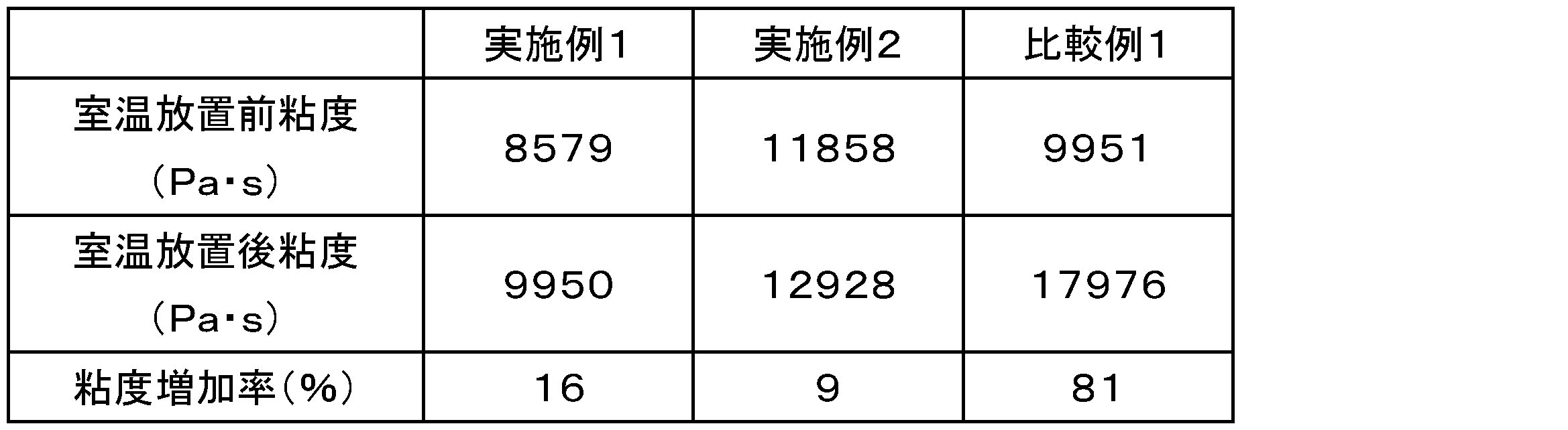
- the shear viscosity of the obtained measurement sample was measured by a dynamic shear viscoelasticity measuring device (trade name “ARES-G2” manufactured by TA Instruments Japan Co., Ltd.). . The measurement was performed at a heating rate of 10 ° C./min, a measuring temperature range of 30 ° C. to 145 ° C., and a frequency of 10 Hz, and the viscosity at 80 ° C. was read. In the same manner, the shear viscosity of the measurement sample left at room temperature (23 ° C., 50% RH) for 4 weeks was measured. Table 2 shows the measurement results of shear viscosity before and after standing at room temperature and the rate of increase in viscosity before and after standing at room temperature.
- the viscosity of the film adhesives of Examples 1 and 2 in which the surface-treated inorganic filler having a glycidyl group accounts for 50% by mass or more of the entire inorganic filler is increased before and after being left at room temperature.
- the rate was 20% or less, and it was confirmed that the increase in viscosity over time was suppressed.
- the increase in viscosity with time is suppressed, and therefore, the mounting property at the time of assembling the semiconductor device hardly deteriorates with time.
- SYMBOLS 10 Semiconductor chip, 15 ... Wiring, 20, 60 ... Substrate, 30 ... Connection bump, 32 ... Bump, 34 ... Through electrode, 40 ... Adhesive material, 50 ... Interposer, 70 ... Solder resist, 100, 200, 300, 400 , 500, 600 ... semiconductor devices.
Landscapes
- Chemical & Material Sciences (AREA)
- Organic Chemistry (AREA)
- Inorganic Chemistry (AREA)
- Adhesives Or Adhesive Processes (AREA)
- Wire Bonding (AREA)
- Structures Or Materials For Encapsulating Or Coating Semiconductor Devices Or Solid State Devices (AREA)
- Adhesive Tapes (AREA)
Abstract
Description
本実施形態に係る半導体用接着剤は、(a)無機フィラー(以下、場合により「(a)成分」という。)を含有する。上記(a)無機フィラーは、グリシジル基を有する表面処理が施された無機フィラーを、(a)無機フィラー全量を基準として50質量%以上含む。また、本実施形態に係る半導体用接着剤は、(b)エポキシ樹脂(以下、場合により「(b)成分」という。)、(c)硬化剤(以下、場合により「(c)成分」という。)、及び、(d)重量平均分子量10000以上の高分子量成分(以下、場合により「(d)成分」という。)のうちの1種以上を含有していてもよい。更に、本実施形態に係る半導体用接着剤は、(e)フラックス剤(以下、場合により「(e)成分」という。)を含有していてもよい。以下、各成分について説明する。
(a)成分の無機フィラーとしては、絶縁性無機フィラー等が挙げられる。中でも、平均粒径100nm以下の無機フィラーであればより好ましい。絶縁性無機フィラーの材質としては、ガラス、シリカ、アルミナ、シリカ・アルミナ、酸化チタン、マイカ、窒化ホウ素等が挙げられ、その中でも、シリカ、アルミナ、シリカ・アルミナ、酸化チタン、窒化ホウ素が好ましく、シリカ、アルミナ、窒化ホウ素がより好ましい。絶縁性無機フィラーは、ウィスカーであってもよく、ウィスカーの材質としては、ホウ酸アルミニウム、チタン酸アルミニウム、酸化亜鉛、珪酸カルシウム、硫酸マグネシウム、窒化ホウ素等が挙げられる。絶縁性無機フィラーは、1種単独で又は2種以上を組み合わせて用いることができる。

(b)成分のエポキシ樹脂としては、分子内に2個以上のエポキシ基を有するエポキシ樹脂が挙げられ、ビスフェノールA型エポキシ樹脂、ビスフェノールF型エポキシ樹脂、ナフタレン型エポキシ樹脂、フェノールノボラック型エポキシ樹脂、クレゾールノボラック型エポキシ樹脂、フェノールアラルキル型エポキシ樹脂、ビフェニル型エポキシ樹脂、トリフェニルメタン型エポキシ樹脂、ジシクロペンタジエン型エポキシ樹脂、各種多官能エポキシ樹脂等を使用することができる。(b)成分は、1種単独で又は2種以上を組み合わせて用いることができる。
(c)硬化剤としては、フェノール樹脂系硬化剤、酸無水物系硬化剤、アミン系硬化剤、イミダゾール系硬化剤及びホスフィン系硬化剤等が挙げられる。(c)成分がフェノール性水酸基、酸無水物、アミン類又はイミダゾール類を含むと、接続部に酸化膜が生じることを抑制するフラックス活性を示しやすく、接続信頼性及び絶縁信頼性を容易に向上させることができる。以下、各硬化剤について説明する。
フェノール樹脂系硬化剤としては、分子内に2個以上のフェノール性水酸基を有する硬化剤が挙げられ、フェノールノボラック樹脂、クレゾールノボラック樹脂、フェノールアラルキル樹脂、クレゾールナフトールホルムアルデヒド重縮合物、トリフェニルメタン型多官能フェノール樹脂、各種多官能フェノール樹脂等を使用することができる。フェノール樹脂系硬化剤は、1種単独で又は2種以上を組み合わせて用いることができる。
酸無水物系硬化剤としては、メチルシクロヘキサンテトラカルボン酸二無水物、無水トリメリット酸、無水ピロメリット酸、ベンゾフェノンテトラカルボン酸二無水物、エチレングリコールビスアンヒドロトリメリテート等を使用することができる。酸無水物系硬化剤は、1種単独で又は2種以上を組み合わせて用いることができる。
アミン系硬化剤としては、ジシアンジアミド、各種アミン化合物等を使用することができる。
イミダゾール系硬化剤としては、2-フェニルイミダゾール、2-フェニル-4-メチルイミダゾール、1-ベンジル-2-メチルイミダゾール、1-ベンジル-2-フェニルイミダゾール、1-シアノエチル-2-ウンデシルイミダゾール、1-シアノ-2-フェニルイミダゾール、1-シアノエチル-2-ウンデシルイミダゾールトリメリテイト、1-シアノエチル-2-フェニルイミダゾリウムトリメリテイト、2,4-ジアミノ-6-[2’-メチルイミダゾリル-(1’)]-エチル-s-トリアジン、2,4-ジアミノ-6-[2’-ウンデシルイミダゾリル-(1’)]-エチル-s-トリアジン、2,4-ジアミノ-6-[2’-エチル-4’-メチルイミダゾリル-(1’)]-エチル-s-トリアジン、2,4-ジアミノ-6-[2’-メチルイミダゾリル-(1’)]-エチル-s-トリアジンイソシアヌル酸付加体、2-フェニルイミダゾールイソシアヌル酸付加体、2-フェニル-4,5-ジヒドロキシメチルイミダゾール、2-フェニル-4-メチル-5-ヒドロキシメチルイミダゾール、エポキシ樹脂とイミダゾール類の付加体等が挙げられる。これらの中でも、硬化性、保存安定性及び接続信頼性にさらに優れる観点から、1-シアノエチル-2-ウンデシルイミダゾール、1-シアノ-2-フェニルイミダゾール、1-シアノエチル-2-ウンデシルイミダゾールトリメリテイト、1-シアノエチル-2-フェニルイミダゾリウムトリメリテイト、2,4-ジアミノ-6-[2’-メチルイミダゾリル-(1’)]-エチル-s-トリアジン、2,4-ジアミノ-6-[2’-エチル-4’-メチルイミダゾリル-(1’)]-エチル-s-トリアジン、2,4-ジアミノ-6-[2’-メチルイミダゾリル-(1’)]-エチル-s-トリアジンイソシアヌル酸付加体、2-フェニルイミダゾールイソシアヌル酸付加体、2-フェニル-4,5-ジヒドロキシメチルイミダゾール及び2-フェニル-4-メチル-5-ヒドロキシメチルイミダゾールが好ましい。イミダゾール系硬化剤は、1種単独で又は2種以上を組み合わせて用いることができる。また、これらをマイクロカプセル化した潜在性硬化剤としてもよい。
ホスフィン系硬化剤としては、トリフェニルホスフィン、テトラフェニルホスホニウムテトラフェニルボレート、テトラフェニルホスホニウムテトラ(4-メチルフェニル)ボレート及びテトラフェニルホスホニウム(4-フルオロフェニル)ボレート等が挙げられる。
(d)重量平均分子量10000以上の高分子量成分((b)成分に該当する化合物を除く)としては、フェノキシ樹脂、ポリイミド樹脂、ポリアミド樹脂、ポリカルボジイミド樹脂、シアネートエステル樹脂、(メタ)アクリル樹脂、ポリエステル樹脂、ポリエチレン樹脂、ポリエーテルスルホン樹脂、ポリエーテルイミド樹脂、ポリビニルアセタール樹脂、ポリウレタン樹脂、アクリルゴム等が挙げられ、その中でも、耐熱性及びフィルム形成性に優れる観点から、フェノキシ樹脂、ポリイミド樹脂、(メタ)アクリル樹脂、アクリルゴム、シアネートエステル樹脂、ポリカルボジイミド樹脂が好ましく、フェノキシ樹脂、ポリイミド樹脂、(メタ)アクリル樹脂、アクリルゴムがより好ましく、フェノキシ樹脂が更に好ましい。(d)成分は、単独又は2種以上の混合体又は共重合体として使用することもできる。
半導体用接着剤は、フラックス活性(酸化物、不純物等を除去する活性)を示す化合物である(e)フラックス剤をさらに含有することができる。フラックス剤としては、非共有電子対を有する含窒素化合物(イミダゾール類、アミン類等。ただし、(c)成分に含まれるものを除く)、カルボン酸類、フェノール類及びアルコール類等が挙げられる。なお、アルコール類に比べてカルボン酸類の方がフラックス活性を強く発現し、接続性を向上し易い。
本実施形態に係る半導体用接着剤は、生産性が向上する観点から、フィルム状(フィルム状接着剤)であることが好ましい。フィルム状接着剤の作製方法を以下に説明する。
本実施形態に係る半導体用接着剤は、半導体装置に好適に用いられ、半導体チップ及び配線回路基板のそれぞれの接続部の電極同士が互いに電気的に接続された半導体装置、又は複数の半導体チップのそれぞれの接続部の電極同士が互いに電気的に接続された半導体装置において、接続部の封止に特に好適に用いられる。以下、本実施形態に係る半導体用接着剤を用いた半導体装置について説明する。半導体装置における接続部の電極同士は、バンプと配線との金属接合、及び、バンプとバンプとの金属接合のいずれでもよい。半導体装置では、例えば、半導体用接着剤を介して電気的な接続を得るフリップチップ接続が用いられてよい。
本実施形態に係る半導体装置の製造方法は、本実施形態に係る半導体用接着剤を用いて、半導体チップ及び配線回路基板、又は、複数の半導体チップ同士を接続する。本実施形態に係る半導体装置の製造方法は、例えば、半導体用接着剤を介して半導体チップ及び配線回路基板を互いに接続すると共に半導体チップ及び配線回路基板のそれぞれの接続部を互いに電気的に接続して半導体装置を得る工程、又は、半導体用接着剤を介して複数の半導体チップを互いに接続すると共に複数の半導体チップのそれぞれの接続部を互いに電気的に接続して半導体装置を得る工程を備える。
積層体を、仮圧着用押圧部材とは別に準備された、対向する一対の本圧着用押圧部材で挟むことによって加熱及び加圧し、それにより半導体チップの接続部と基板又は他の半導体チップの接続部とを金属接合によって電気的に接続する。この場合、一対の本圧着用押圧部材のうち少なくとも一方が、積層体を加熱及び加圧する時に、半導体チップの接続部の表面を形成している金属材料の融点、又は基板若しくは他の半導体チップの接続部の表面を形成している金属材料の融点のうち少なくともいずれか一方の融点以上の温度に加熱される。
ステージ上に配置された複数の積層体又は複数の半導体チップ、半導体ウエハ及び接着剤を有する積層体とそれらを覆うように配置された一括接続用シートとを、ステージと該ステージに対向する圧着ヘッドとで挟むことによって一括して複数の積層体を加熱及び加圧し、それにより半導体チップの接続部と基板又は他の半導体チップの接続部とを金属接合によって電気的に接続する。この場合、ステージ及び圧着ヘッドのうち少なくとも一方が、半導体チップの接続部の表面を形成している金属材料の融点、又は基板若しくは他の半導体チップの接続部の表面を形成している金属材料の融点のうち少なくともいずれか一方の融点以上の温度に加熱される。
積層体を、加熱炉内又はホットプレート上で、半導体チップの接続部の表面を形成している金属材料の融点、又は基板若しくは他の半導体チップの接続部の表面を形成している金属材料の融点のうち少なくともいずれか一方の融点以上の温度に加熱する。
(a)無機フィラー
・エポキシ表面処理ナノシリカフィラー(グリシジル基を有する表面処理が施された無機フィラー、株式会社アドマテックス製、商品名「50nm SE-AH1」、平均粒径:約50nm、以下「SEナノシリカ」という。)
・メタクリル表面処理ナノシリカフィラー(株式会社アドマテックス製、商品名「50nm YA050C-HGF」、平均粒径:約50nm、以下「YAナノシリカ」という。)
・トリフェノールメタン骨格含有多官能固形エポキシ樹脂(三菱ケミカル株式会社製、商品名「EP1032H60」、以下「EP1032」という。)
・柔軟性エポキシ樹脂(三菱ケミカル株式会社製、商品名「YL7175」、以下「YL7175」という。)
・2,4-ジアミノ-6-[2’-メチルイミダゾリル-(1’)]-エチル-s-トリアジンイソシアヌル酸付加体(四国化成工業株式会社製、商品名「2MAOK-PW」、以下「2MAOK」という。)
・アクリル樹脂(株式会社クラレ製、商品名「クラリティLA4285」、Mw/Mn=1.28、重量平均分子量Mw:80000、以下「LA4285」という。)
・グルタル酸(シグマアルドリッチジャパン合同会社製、融点:約97℃)
(実施例1)
エポキシ樹脂「EP1032」12.4g、「YL7175」0.72g、硬化剤「2MAOK」0.9g、グルタル酸1.2g、無機フィラー「SEナノシリカ」33.9g、アクリル樹脂「LA4285」6.0g、及び、シクロヘキサノン(樹脂ワニス中の固形分量が49質量%になる量)を仕込み、直径1.0mmのジルコニアビーズを固形分と同質量加え、ビーズミル(フリッチュ・ジャパン株式会社製、遊星型微粉砕機P-7)で30分撹拌した。その後、撹拌に用いたジルコニアビーズをろ過によって除去し、樹脂ワニスを得た。
無機フィラー「SEナノシリカ」を17gに減らし、無機フィラー「YAナノシリカ」を17g加えたこと以外は、実施例1と同様にして、フィルム状接着剤を作製した。
無機フィラー「SEナノシリカ」をなくし、無機フィラー「YAナノシリカ」を33.9g加えたこと以外は、実施例1と同様にして、フィルム状接着剤を作製した。
以下、実施例及び比較例で得られたフィルム状接着剤の評価方法を示す。
作製したフィルム状接着剤を卓上ラミネータ(株式会社ミラーコーポレーション製、商品名「ホットドッグGK-13DX」)にて、総厚が0.4mm(400μm)になるまで複数枚ラミネート(積層)し、縦7.3mm、横7.3mmサイズに切り抜き、測定サンプルを得た。
得られた測定サンプルのずり粘度を、動的ずり粘弾性測定装置(ティー・エイ・インスツルメント・ジャパン株式会社製、商品名「ARES-G2」)にて測定した。測定条件は、昇温速度10℃/分、測定温度範囲30℃~145℃、周波数10Hzで行い、80℃での粘度値を読み取った。同様の方法で、室温(23℃、50%RH)で4週間放置後の測定サンプルについて、ずり粘度の測定を行った。室温放置前後のずり粘度の測定結果、及び、室温放置前後の粘度増加率を表2に示す。

Claims (6)
- (a)無機フィラーを含有し、前記(a)無機フィラーが、グリシジル基を有する表面処理が施された無機フィラーを、前記(a)無機フィラー全量を基準として50質量%以上含む、半導体用接着剤。
- (b)エポキシ樹脂、(c)硬化剤、及び、(d)重量平均分子量10000以上の高分子量成分を更に含有する、請求項1に記載の半導体用接着剤。
- (e)フラックス剤を更に含有する、請求項1又は2に記載の半導体用接着剤。
- フィルム状である、請求項1~3のいずれか一項に記載の半導体用接着剤。
- 半導体チップ及び配線回路基板のそれぞれの接続部が互いに電気的に接続された半導体装置、又は、複数の半導体チップのそれぞれの接続部が互いに電気的に接続された半導体装置の製造方法であって、
前記接続部の少なくとも一部を、請求項1~4のいずれか一項に記載の半導体用接着剤を用いて封止する工程を備える、半導体装置の製造方法。 - 半導体チップ及び配線回路基板のそれぞれの接続部が互いに電気的に接続された接続構造、又は、複数の半導体チップのそれぞれの接続部が互いに電気的に接続された接続構造と、
前記接続部の少なくとも一部を封止する接着材料と、を備え、
前記接着材料は、請求項1~4のいずれか一項に記載の半導体用接着剤の硬化物からなる、半導体装置。
Priority Applications (3)
| Application Number | Priority Date | Filing Date | Title |
|---|---|---|---|
| JP2020550470A JP7363798B2 (ja) | 2018-10-02 | 2019-10-01 | 半導体用接着剤、半導体装置の製造方法及び半導体装置 |
| CN201980062245.8A CN112771659B (zh) | 2018-10-02 | 2019-10-01 | 半导体用黏合剂、半导体装置的制造方法及半导体装置 |
| KR1020217008276A KR102629861B1 (ko) | 2018-10-02 | 2019-10-01 | 반도체용 접착제, 반도체 장치의 제조 방법 및 반도체 장치 |
Applications Claiming Priority (2)
| Application Number | Priority Date | Filing Date | Title |
|---|---|---|---|
| JP2018187510 | 2018-10-02 | ||
| JP2018-187510 | 2018-10-02 |
Publications (1)
| Publication Number | Publication Date |
|---|---|
| WO2020071391A1 true WO2020071391A1 (ja) | 2020-04-09 |
Family
ID=70054548
Family Applications (1)
| Application Number | Title | Priority Date | Filing Date |
|---|---|---|---|
| PCT/JP2019/038821 Ceased WO2020071391A1 (ja) | 2018-10-02 | 2019-10-01 | 半導体用接着剤、半導体装置の製造方法及び半導体装置 |
Country Status (5)
| Country | Link |
|---|---|
| JP (1) | JP7363798B2 (ja) |
| KR (1) | KR102629861B1 (ja) |
| CN (1) | CN112771659B (ja) |
| TW (2) | TWI875717B (ja) |
| WO (1) | WO2020071391A1 (ja) |
Cited By (2)
| Publication number | Priority date | Publication date | Assignee | Title |
|---|---|---|---|---|
| JP2020164792A (ja) * | 2019-03-26 | 2020-10-08 | 日東電工株式会社 | 透明接着シートおよび剥離材付き透明接着シート |
| CN116194546A (zh) * | 2020-09-16 | 2023-05-30 | 株式会社力森诺科 | 半导体用黏合剂、以及半导体装置及其制造方法 |
Families Citing this family (1)
| Publication number | Priority date | Publication date | Assignee | Title |
|---|---|---|---|---|
| TWI767537B (zh) * | 2021-01-26 | 2022-06-11 | 隆達電子股份有限公司 | 發光二極體封裝結構的製造方法 |
Citations (2)
| Publication number | Priority date | Publication date | Assignee | Title |
|---|---|---|---|---|
| JP2013038175A (ja) * | 2011-08-05 | 2013-02-21 | Hitachi Chem Co Ltd | 半導体装置の製造方法、フィルム状接着剤及び接着剤シート |
| JP2017041499A (ja) * | 2015-08-18 | 2017-02-23 | 日立化成株式会社 | 半導体用接着剤、並びに、半導体装置及びその製造方法 |
Family Cites Families (12)
| Publication number | Priority date | Publication date | Assignee | Title |
|---|---|---|---|---|
| JP5130397B2 (ja) * | 2010-01-21 | 2013-01-30 | 積水化学工業株式会社 | 熱硬化性樹脂組成物、先塗布型フリップチップ実装用接着剤、半導体装置の製造方法、及び、半導体装置 |
| KR101728203B1 (ko) * | 2010-09-30 | 2017-04-18 | 히타치가세이가부시끼가이샤 | 접착제 조성물, 반도체 장치의 제조 방법 및 반도체 장치 |
| JP2012089750A (ja) * | 2010-10-21 | 2012-05-10 | Hitachi Chem Co Ltd | 半導体封止充てん用熱硬化性樹脂組成物及び半導体装置 |
| JP5598343B2 (ja) | 2011-01-17 | 2014-10-01 | 信越化学工業株式会社 | 半導体封止用液状エポキシ樹脂組成物及び半導体装置 |
| JP2013071941A (ja) * | 2011-09-26 | 2013-04-22 | Hitachi Chemical Co Ltd | 半導体封止充てん用エポキシ樹脂組成物、半導体装置の製造方法、半導体装置 |
| JP6047888B2 (ja) | 2012-02-24 | 2016-12-21 | 日立化成株式会社 | 半導体用接着剤及び半導体装置の製造方法 |
| JP6407684B2 (ja) | 2014-11-28 | 2018-10-17 | 日東電工株式会社 | シート状樹脂組成物、積層シート及び半導体装置の製造方法 |
| JP6544146B2 (ja) * | 2015-08-27 | 2019-07-17 | 日立化成株式会社 | 半導体装置及びそれを製造する方法 |
| US10669454B2 (en) * | 2015-10-29 | 2020-06-02 | Hitachi Chemical Company, Ltd. | Method for manufacturing semiconductor device including heating and pressuring a laminate having an adhesive layer |
| JP2017122193A (ja) | 2016-01-08 | 2017-07-13 | 日立化成株式会社 | 半導体用接着剤及び半導体装置の製造方法 |
| JP6717005B2 (ja) | 2016-03-31 | 2020-07-01 | 日立化成株式会社 | 樹脂組成物、硬化物、樹脂フィルム、封止材及び封止構造体 |
| CN107221573B (zh) * | 2017-05-19 | 2019-06-21 | 浙江帝恒实业有限公司 | 一种防紫外老化太阳能电池背板膜及其制备方法 |
-
2019
- 2019-10-01 TW TW108135572A patent/TWI875717B/zh active
- 2019-10-01 WO PCT/JP2019/038821 patent/WO2020071391A1/ja not_active Ceased
- 2019-10-01 KR KR1020217008276A patent/KR102629861B1/ko active Active
- 2019-10-01 CN CN201980062245.8A patent/CN112771659B/zh active Active
- 2019-10-01 JP JP2020550470A patent/JP7363798B2/ja active Active
- 2019-10-01 TW TW113147436A patent/TWI906069B/zh active
Patent Citations (2)
| Publication number | Priority date | Publication date | Assignee | Title |
|---|---|---|---|---|
| JP2013038175A (ja) * | 2011-08-05 | 2013-02-21 | Hitachi Chem Co Ltd | 半導体装置の製造方法、フィルム状接着剤及び接着剤シート |
| JP2017041499A (ja) * | 2015-08-18 | 2017-02-23 | 日立化成株式会社 | 半導体用接着剤、並びに、半導体装置及びその製造方法 |
Cited By (4)
| Publication number | Priority date | Publication date | Assignee | Title |
|---|---|---|---|---|
| JP2020164792A (ja) * | 2019-03-26 | 2020-10-08 | 日東電工株式会社 | 透明接着シートおよび剥離材付き透明接着シート |
| JP7612332B2 (ja) | 2019-03-26 | 2025-01-14 | 日東電工株式会社 | 透明接着シートおよび剥離材付き透明接着シート |
| CN116194546A (zh) * | 2020-09-16 | 2023-05-30 | 株式会社力森诺科 | 半导体用黏合剂、以及半导体装置及其制造方法 |
| TWI874709B (zh) * | 2020-09-16 | 2025-03-01 | 日商力森諾科股份有限公司 | 半導體用接著劑、以及半導體裝置及其製造方法 |
Also Published As
| Publication number | Publication date |
|---|---|
| TWI875717B (zh) | 2025-03-11 |
| KR102629861B1 (ko) | 2024-01-29 |
| TW202511434A (zh) | 2025-03-16 |
| KR20210068412A (ko) | 2021-06-09 |
| JP7363798B2 (ja) | 2023-10-18 |
| CN112771659A (zh) | 2021-05-07 |
| CN112771659B (zh) | 2025-02-21 |
| TW202033708A (zh) | 2020-09-16 |
| JPWO2020071391A1 (ja) | 2021-09-02 |
| TWI906069B (zh) | 2025-11-21 |
Similar Documents
| Publication | Publication Date | Title |
|---|---|---|
| TWI721150B (zh) | 半導體裝置的製造方法 | |
| WO2013125086A1 (ja) | 半導体用接着剤、フラックス剤、半導体装置の製造方法及び半導体装置 | |
| WO2018225800A1 (ja) | 半導体用フィルム状接着剤、半導体装置の製造方法及び半導体装置 | |
| JP7363798B2 (ja) | 半導体用接着剤、半導体装置の製造方法及び半導体装置 | |
| JP7544031B2 (ja) | 半導体用接着剤、半導体装置の製造方法及び半導体装置 | |
| TWI807135B (zh) | 半導體用膜狀接著劑、半導體裝置及其製造方法 | |
| WO2013125087A1 (ja) | 半導体用接着剤、フラックス剤、半導体装置の製造方法及び半導体装置 | |
| JP2017171817A (ja) | 半導体用接着剤、半導体装置、及び半導体装置の製造方法 | |
| JP2021024963A (ja) | 半導体用接着剤、それを用いた半導体用接着剤フィルムの製造方法及び半導体装置の製造方法 | |
| WO2019123518A1 (ja) | 半導体装置、半導体装置の製造方法及び接着剤 | |
| WO2022102181A1 (ja) | 半導体装置の製造方法及びこれに用いられる接着剤 | |
| JP6690308B2 (ja) | 半導体装置を製造する方法 | |
| JP7248007B2 (ja) | 半導体用接着剤及びそれを用いた半導体装置の製造方法 | |
| WO2024009498A1 (ja) | 半導体装置の製造方法、基板及び半導体素子 | |
| WO2025004894A1 (ja) | 半導体装置を製造する方法 | |
| JP2021061276A (ja) | 半導体装置の製造方法 |
Legal Events
| Date | Code | Title | Description |
|---|---|---|---|
| 121 | Ep: the epo has been informed by wipo that ep was designated in this application |
Ref document number: 19868569 Country of ref document: EP Kind code of ref document: A1 |
|
| ENP | Entry into the national phase |
Ref document number: 2020550470 Country of ref document: JP Kind code of ref document: A |
|
| ENP | Entry into the national phase |
Ref document number: 20217008276 Country of ref document: KR Kind code of ref document: A |
|
| NENP | Non-entry into the national phase |
Ref country code: DE |
|
| 122 | Ep: pct application non-entry in european phase |
Ref document number: 19868569 Country of ref document: EP Kind code of ref document: A1 |
|
| WWG | Wipo information: grant in national office |
Ref document number: 201980062245.8 Country of ref document: CN |