WO2020066760A1 - 光スイッチング素子 - Google Patents
光スイッチング素子 Download PDFInfo
- Publication number
- WO2020066760A1 WO2020066760A1 PCT/JP2019/036440 JP2019036440W WO2020066760A1 WO 2020066760 A1 WO2020066760 A1 WO 2020066760A1 JP 2019036440 W JP2019036440 W JP 2019036440W WO 2020066760 A1 WO2020066760 A1 WO 2020066760A1
- Authority
- WO
- WIPO (PCT)
- Prior art keywords
- film
- substrate
- pixel
- region
- reflection
- Prior art date
- Legal status (The legal status is an assumption and is not a legal conclusion. Google has not performed a legal analysis and makes no representation as to the accuracy of the status listed.)
- Ceased
Links
Images



Classifications
-
- G—PHYSICS
- G02—OPTICS
- G02F—OPTICAL DEVICES OR ARRANGEMENTS FOR THE CONTROL OF LIGHT BY MODIFICATION OF THE OPTICAL PROPERTIES OF THE MEDIA OF THE ELEMENTS INVOLVED THEREIN; NON-LINEAR OPTICS; FREQUENCY-CHANGING OF LIGHT; OPTICAL LOGIC ELEMENTS; OPTICAL ANALOGUE/DIGITAL CONVERTERS
- G02F1/00—Devices or arrangements for the control of the intensity, colour, phase, polarisation or direction of light arriving from an independent light source, e.g. switching, gating or modulating; Non-linear optics
- G02F1/01—Devices or arrangements for the control of the intensity, colour, phase, polarisation or direction of light arriving from an independent light source, e.g. switching, gating or modulating; Non-linear optics for the control of the intensity, phase, polarisation or colour
- G02F1/13—Devices or arrangements for the control of the intensity, colour, phase, polarisation or direction of light arriving from an independent light source, e.g. switching, gating or modulating; Non-linear optics for the control of the intensity, phase, polarisation or colour based on liquid crystals, e.g. single liquid crystal display cells
- G02F1/133—Constructional arrangements; Operation of liquid crystal cells; Circuit arrangements
- G02F1/1333—Constructional arrangements; Manufacturing methods
- G02F1/1335—Structural association of cells with optical devices, e.g. polarisers or reflectors
- G02F1/133528—Polarisers
- G02F1/133545—Dielectric stack polarisers
-
- G—PHYSICS
- G02—OPTICS
- G02F—OPTICAL DEVICES OR ARRANGEMENTS FOR THE CONTROL OF LIGHT BY MODIFICATION OF THE OPTICAL PROPERTIES OF THE MEDIA OF THE ELEMENTS INVOLVED THEREIN; NON-LINEAR OPTICS; FREQUENCY-CHANGING OF LIGHT; OPTICAL LOGIC ELEMENTS; OPTICAL ANALOGUE/DIGITAL CONVERTERS
- G02F1/00—Devices or arrangements for the control of the intensity, colour, phase, polarisation or direction of light arriving from an independent light source, e.g. switching, gating or modulating; Non-linear optics
- G02F1/29—Devices or arrangements for the control of the intensity, colour, phase, polarisation or direction of light arriving from an independent light source, e.g. switching, gating or modulating; Non-linear optics for the control of the position or the direction of light beams, i.e. deflection
- G02F1/31—Digital deflection, i.e. optical switching
-
- G—PHYSICS
- G02—OPTICS
- G02F—OPTICAL DEVICES OR ARRANGEMENTS FOR THE CONTROL OF LIGHT BY MODIFICATION OF THE OPTICAL PROPERTIES OF THE MEDIA OF THE ELEMENTS INVOLVED THEREIN; NON-LINEAR OPTICS; FREQUENCY-CHANGING OF LIGHT; OPTICAL LOGIC ELEMENTS; OPTICAL ANALOGUE/DIGITAL CONVERTERS
- G02F1/00—Devices or arrangements for the control of the intensity, colour, phase, polarisation or direction of light arriving from an independent light source, e.g. switching, gating or modulating; Non-linear optics
- G02F1/01—Devices or arrangements for the control of the intensity, colour, phase, polarisation or direction of light arriving from an independent light source, e.g. switching, gating or modulating; Non-linear optics for the control of the intensity, phase, polarisation or colour
- G02F1/13—Devices or arrangements for the control of the intensity, colour, phase, polarisation or direction of light arriving from an independent light source, e.g. switching, gating or modulating; Non-linear optics for the control of the intensity, phase, polarisation or colour based on liquid crystals, e.g. single liquid crystal display cells
-
- G—PHYSICS
- G02—OPTICS
- G02F—OPTICAL DEVICES OR ARRANGEMENTS FOR THE CONTROL OF LIGHT BY MODIFICATION OF THE OPTICAL PROPERTIES OF THE MEDIA OF THE ELEMENTS INVOLVED THEREIN; NON-LINEAR OPTICS; FREQUENCY-CHANGING OF LIGHT; OPTICAL LOGIC ELEMENTS; OPTICAL ANALOGUE/DIGITAL CONVERTERS
- G02F1/00—Devices or arrangements for the control of the intensity, colour, phase, polarisation or direction of light arriving from an independent light source, e.g. switching, gating or modulating; Non-linear optics
- G02F1/01—Devices or arrangements for the control of the intensity, colour, phase, polarisation or direction of light arriving from an independent light source, e.g. switching, gating or modulating; Non-linear optics for the control of the intensity, phase, polarisation or colour
- G02F1/13—Devices or arrangements for the control of the intensity, colour, phase, polarisation or direction of light arriving from an independent light source, e.g. switching, gating or modulating; Non-linear optics for the control of the intensity, phase, polarisation or colour based on liquid crystals, e.g. single liquid crystal display cells
- G02F1/133—Constructional arrangements; Operation of liquid crystal cells; Circuit arrangements
- G02F1/1333—Constructional arrangements; Manufacturing methods
- G02F1/1335—Structural association of cells with optical devices, e.g. polarisers or reflectors
-
- G—PHYSICS
- G02—OPTICS
- G02F—OPTICAL DEVICES OR ARRANGEMENTS FOR THE CONTROL OF LIGHT BY MODIFICATION OF THE OPTICAL PROPERTIES OF THE MEDIA OF THE ELEMENTS INVOLVED THEREIN; NON-LINEAR OPTICS; FREQUENCY-CHANGING OF LIGHT; OPTICAL LOGIC ELEMENTS; OPTICAL ANALOGUE/DIGITAL CONVERTERS
- G02F1/00—Devices or arrangements for the control of the intensity, colour, phase, polarisation or direction of light arriving from an independent light source, e.g. switching, gating or modulating; Non-linear optics
- G02F1/01—Devices or arrangements for the control of the intensity, colour, phase, polarisation or direction of light arriving from an independent light source, e.g. switching, gating or modulating; Non-linear optics for the control of the intensity, phase, polarisation or colour
- G02F1/13—Devices or arrangements for the control of the intensity, colour, phase, polarisation or direction of light arriving from an independent light source, e.g. switching, gating or modulating; Non-linear optics for the control of the intensity, phase, polarisation or colour based on liquid crystals, e.g. single liquid crystal display cells
- G02F1/133—Constructional arrangements; Operation of liquid crystal cells; Circuit arrangements
- G02F1/1333—Constructional arrangements; Manufacturing methods
- G02F1/1335—Structural association of cells with optical devices, e.g. polarisers or reflectors
- G02F1/133553—Reflecting elements
-
- G—PHYSICS
- G02—OPTICS
- G02F—OPTICAL DEVICES OR ARRANGEMENTS FOR THE CONTROL OF LIGHT BY MODIFICATION OF THE OPTICAL PROPERTIES OF THE MEDIA OF THE ELEMENTS INVOLVED THEREIN; NON-LINEAR OPTICS; FREQUENCY-CHANGING OF LIGHT; OPTICAL LOGIC ELEMENTS; OPTICAL ANALOGUE/DIGITAL CONVERTERS
- G02F1/00—Devices or arrangements for the control of the intensity, colour, phase, polarisation or direction of light arriving from an independent light source, e.g. switching, gating or modulating; Non-linear optics
- G02F1/01—Devices or arrangements for the control of the intensity, colour, phase, polarisation or direction of light arriving from an independent light source, e.g. switching, gating or modulating; Non-linear optics for the control of the intensity, phase, polarisation or colour
- G02F1/13—Devices or arrangements for the control of the intensity, colour, phase, polarisation or direction of light arriving from an independent light source, e.g. switching, gating or modulating; Non-linear optics for the control of the intensity, phase, polarisation or colour based on liquid crystals, e.g. single liquid crystal display cells
- G02F1/133—Constructional arrangements; Operation of liquid crystal cells; Circuit arrangements
- G02F1/1333—Constructional arrangements; Manufacturing methods
- G02F1/1335—Structural association of cells with optical devices, e.g. polarisers or reflectors
- G02F1/133528—Polarisers
- G02F1/133536—Reflective polarizers
-
- G—PHYSICS
- G02—OPTICS
- G02F—OPTICAL DEVICES OR ARRANGEMENTS FOR THE CONTROL OF LIGHT BY MODIFICATION OF THE OPTICAL PROPERTIES OF THE MEDIA OF THE ELEMENTS INVOLVED THEREIN; NON-LINEAR OPTICS; FREQUENCY-CHANGING OF LIGHT; OPTICAL LOGIC ELEMENTS; OPTICAL ANALOGUE/DIGITAL CONVERTERS
- G02F2201/00—Constructional arrangements not provided for in groups G02F1/00 - G02F7/00
- G02F2201/12—Constructional arrangements not provided for in groups G02F1/00 - G02F7/00 electrode
- G02F2201/123—Constructional arrangements not provided for in groups G02F1/00 - G02F7/00 electrode pixel
Definitions
- the present invention relates to the structure of the reflection-enhancing film of the optical switching element.
- a WSS (Wavelength Selective Switch) device is used as an optical switching device in the ROADM device.
- the WSS device can select and assign an arbitrary wavelength to an arbitrary input / output port for an optical signal including a plurality of wavelengths, and can input / output wavelength multiplexing.
- a MEMS (Micro Electro Mechanical Systems) mirror and an LCOS (Liquid Crystal on silicon) element are used as an optical switching element in the WSS device.
- the LCOS element is a reflection type liquid crystal element having a pixel region in which a plurality of reflection type pixel electrodes are arranged in a horizontal direction and a vertical direction.
- the refractive index of the liquid crystal on each pixel electrode changes by controlling the voltage applied to the liquid crystal for each pixel electrode.
- the phase speed of the signal light is controlled for each pixel by changing the refractive index of the liquid crystal on each pixel.
- the LCOS element can control the inclination angle of the wavefront of the signal light in accordance with the rate of change of the phase speed by changing the phase speed stepwise for each pixel. That is, the LCOS element functions as a phase modulation element that changes the phase speed for each pixel and reflects the signal light in a predetermined direction.
- dielectric films having different refractive indices are alternately stacked on the plurality of pixel electrodes, and a reflection-enhancing film for increasing the reflectivity by the interference of light is formed to efficiently reflect the wavelength of the signal light.
- a reflection-enhancing film for increasing the reflectivity by the interference of light is formed to efficiently reflect the wavelength of the signal light.
- the MEMS mirror In the MEMS mirror, mirrors corresponding to the number of wavelength bands of the signal light are required. Therefore, when the wavelength band of the signal light or the number of the wavelength bands of the signal light is changed, a MEMS mirror must be newly manufactured according to the change.
- the LCOS element can arbitrarily divide the pixel area into a plurality of pixel blocks and control the pixel blocks. Accordingly, when the wavelength band of the signal light or the number of the wavelength bands of the signal light is changed, the pixel block can be reconfigured according to the changed content, so that it is not necessary to newly manufacture an LCOS element. That is, the LCOS element has better variable grid properties than the MEMS mirror.
- Patent Literature 1 discloses an example of a phase modulation device using an LCOS element. Patent Literature 1 describes a method of correcting a voltage applied to a pixel for the purpose of suppressing phase crosstalk of an LCOS element, but does not describe a method of controlling the thickness of a liquid crystal layer to make the applied voltage uniform.
- the LCOS element When an LCOS element is used as an optical switching element in a WSS device, the LCOS element reflects signal light in a predetermined direction by phase modulation.
- the liquid crystal layer of the LCOS element needs to have a thickness of about 5 ⁇ m in order to secure 2 ⁇ phase modulation.
- the reflection-enhancing film on the plurality of pixel electrodes arranged on the driving substrate is formed by laminating about five pairs (10 layers) of dielectric films, and has a thickness of about 0.5 ⁇ m.
- the sealing material used for bonding the transparent substrate facing the driving substrate has an appropriate fluidity, so that the sealing material flows out of a predetermined application position, flows into the pixel region, and ends of the reflection-enhancing film. (Boundary) or the outermost surface.
- the sealing material may run on the film edge (boundary) or the step on the outermost surface of the reflection-enhancing film. Therefore, in the pixel region, the thickness of the liquid crystal layer including the driving substrate and the transparent substrate on which the enhanced reflection film is the outermost surface may be uneven.
- the present invention provides an optical switching element capable of suppressing deterioration in performance of an optical switching element due to uneven thickness of a liquid crystal layer when an LCOS element having an enhanced reflection film is used as the optical switching element. Aim.
- One embodiment of the present invention is a driving substrate having a pixel region including a plurality of pixel electrodes, an outer peripheral region disposed outside the pixel region, a sealing region, a transparent substrate having a counter electrode, and the driving substrate And a liquid crystal layer sandwiched between the transparent substrate and a reflective film disposed on the entire surface of the driving substrate, wherein the reflective film comprises two stacked dielectric films having different refractive indices. Is formed by laminating one or more aggregates of the dielectric films, and a flattening process is performed on the first dielectric film constituting the enhanced reflection film. An optical switching element is provided.
- One embodiment of the present invention is a driving substrate having a pixel region including a plurality of pixel electrodes, an outer peripheral region disposed outside the pixel region, a sealing region, a transparent substrate having a counter electrode, and the driving substrate And a liquid crystal layer sandwiched between the transparent substrate and the pixel region, the outer peripheral region, and an enhanced reflection film disposed on an upper surface of the seal region.
- the enhanced reflection film has a different refractive index.
- An aggregate of the dielectric films which is a set of two laminated dielectric films, is formed by laminating one or more dielectric films. To provide an optical switching element which has been subjected to a flattening process.
- the structure of the reflection-enhancing film of the optical switching element of the present invention when the LCOS element is used as the optical switching element, it is possible to suppress the deterioration of the performance of the optical switching element due to the uneven thickness of the liquid crystal layer. .
- FIG. 1 is a top view showing a film formation region of an enhanced reflection film of the optical switching element of the present embodiment.
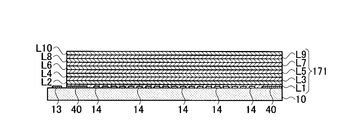
- FIG. 2 is a cross-sectional view illustrating an example of the configuration of the reflection-enhancing film of the optical switching element of the present embodiment.
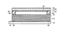
- FIG. 3 is a diagram showing a regular positional relationship among the driving substrate, the transparent substrate, and the sealing material of the optical switching element according to the present embodiment.
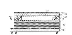
- FIG. 4 is a diagram showing a positional relationship in which the sealing material has deviated from the sealing region when the driving substrate and the transparent substrate of the optical switching element of the present embodiment are bonded together.
- FIG. 5 is a cross-sectional view illustrating a configuration example of the optical switching element of the present embodiment.
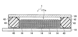
- FIG. 6A is a diagram illustrating a regular positional relationship among a driving substrate, a transparent substrate, and a sealing material of the optical switching element.
- FIG. 6B is a diagram illustrating a positional relationship between the driving substrate and the positioning jig.
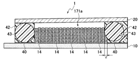
- FIG. 6C is a diagram showing a positional relationship between the driving substrate, the transparent substrate, and the sealing material of the optical switching element of the related art when the bonding is abnormal.
- FIG. 6D is a diagram illustrating a positional relationship between the driving substrate, the transparent substrate, and the sealing material of the optical switching element of the related art when the bonding is abnormal.
- optical switching element A configuration example of the optical switching element will be described with reference to FIGS.
- the optical switching element is, for example, an LCOS element that is a reflective liquid crystal element.
- the optical switching element 2 includes a driving substrate 10, a transparent substrate 20, a liquid crystal 31 filled in a liquid crystal layer 30, and a spacer material 43 applied to a sealing region 40.
- a sealing material 42 and a sealing material 50 are provided.
- the drive substrate 10 is a first substrate
- the transparent substrate 20 is a second substrate.
- the sealing material 42 and the sealing material 50 are a photocurable resin, for example, an ultraviolet curable resin.
- the sealing material 42 and the sealing material 50 may be the same type of photocurable resin, or may be different types of photocurable resin.
- the drive substrate 10 has a pixel area 11, an outer peripheral area 18, and a seal area 40.
- a plurality of pixel electrodes 14 having light reflectivity are arranged in the horizontal and vertical directions.
- One pixel electrode 14 constitutes one pixel.
- the outer peripheral area 18 surrounds the pixel area 11.
- the seal area 40 surrounds the outer peripheral area 18.
- the reflection enhancing film 171 is formed on at least the pixel region 11 among the pixel region 11, the outer peripheral region 18, and the seal region 40.
- the alignment film 12 is formed at least on the reflection increasing film 171.
- the plurality of connection terminals 13 are formed on the outer peripheral portion of the drive board 10.
- the drive substrate 10 is a semiconductor substrate, specifically, a silicon substrate.
- a drive circuit for driving each pixel is formed on the drive substrate 10 below each pixel electrode 14 (not shown).
- Aluminum or an aluminum alloy may be used as a material of the pixel electrode 14 and the connection terminal 13.
- the transparent substrate 20 has a counter electrode 21 and an alignment film 22.
- the counter electrode 21 corresponds to the plurality of pixel electrodes 14.
- the alignment film 22 is formed on the counter electrode 21.
- the drive substrate 10 and the transparent substrate 20 are arranged so that the plurality of pixel electrodes 14 and the counter electrode 21 face each other.
- the drive substrate 10 and the transparent substrate 20 are fixed with a gap GP by a sealant 42 and a sealant 50.
- a liquid crystal layer 30 is formed in a gap GP between the driving substrate 10 and the transparent substrate 20.
- the liquid crystal layer 30 is formed on an aggregate of the plurality of pixel electrodes 14, the reflective film 171, and the alignment film 12.
- An antireflection film 23 may be formed on the surface of the transparent substrate 20 opposite to the surface on which the counter electrode 21 is formed. As the antireflection film 23, a dielectric multilayer film may be used.
- the transparent substrate 20, the counter electrode 21, and the alignment film 22 have optical transparency.
- An alkali-free glass substrate or a quartz glass substrate may be used as the transparent substrate 20.
- ITO Indium Tin Oxide
- a dielectric film having optical transparency may be formed on the upper and lower sides of the ITO film.
- the sealing material 42 is applied and formed so as to surround the pixel region 11 and the outer peripheral region 18 along the outer peripheral region 18 which is the outer peripheral portion of the pixel region 11. Further, the liquid crystal injection part 41 is formed in the sealant 42.
- the liquid crystal layer 30 is formed by injecting the liquid crystal 31 from the liquid crystal injection part 41 of the sealing material 42 into the gap GP between the driving substrate 10 and the transparent substrate 20 and sealing the liquid crystal injection part 41 with the sealing material 50. Is done.
- the thickness of the liquid crystal layer 30 in the optical switching element 2 is, for example, 5 ⁇ m.
- a drive signal for driving the liquid crystal 31 is input to a predetermined connection terminal 13 of the plurality of connection terminals 13.
- a drive circuit formed on the drive substrate 10 applies a drive voltage based on a drive signal to each pixel electrode 14. Thereby, the liquid crystal 31 is driven for each pixel according to the potential difference between each pixel electrode 14 and the counter electrode 21.
- the reflection-enhancing film 171 formed on the pixel region 11, the outer peripheral region 18, and the seal region 40 will be described in detail. Since a plurality of pixel electrodes 14 are arranged in the pixel region 11 indicated by oblique lines in FIG. 1, the surface of the pixel region 11 in which only the plurality of pixel electrodes 14 are arranged has an uneven surface shape. As shown in FIG. 2, the reflection-enhancing film 171 is formed by laminating a dielectric thin film made of a dielectric (for example, SiO 2: silicon dioxide) on the outer peripheral region 18 and the seal region 40 of the pixel region 11.
- a dielectric thin film made of a dielectric (for example, SiO 2: silicon dioxide)
- an SiO2 film (L1) serving as a first layer is formed on the outer peripheral region 18 and the seal region 40 of the pixel region 11, by a vacuum film deposition method or the like.
- the formed SiO 2 layer is a thin film having unevenness reflecting the surface shape of the unevenness of the pixel region 11 (lower layer) in which only the plurality of pixel electrodes 14 are arranged.
- the first layer L1 may be formed in a wafer state during a semiconductor manufacturing process for manufacturing the drive substrate 10.
- a flat film shape without unevenness is formed by a chemical mechanical polishing (CMP) method or the like.
- CMP chemical mechanical polishing
- the planarization treatment is described by way of chemical mechanical polishing as an example, the planarization method is not limited to this, and may be performed by a chemical etching method or the like. Note that the flattening process may be performed in a state of a semiconductor wafer.
- a film in which a low-refractive-index film SiO2 (L1) and a high-refractive-index film Si3N4 (L2) are combined is formed as a set, similarly to the related art.
- the dielectric aggregate is repeatedly laminated from L1 to L10 to form the reflection-enhancing film 171.
- FIG. 3 shows a state in which the drive substrate 10 on which the reflection-enhancing film 171 is formed and the transparent substrate 20 are bonded at an appropriate coating position of the sealing material 42.
- FIG. 4 shows a state in which the sealing material 42 is stuck at a position where the application position is out of the sealing region 40.
- FIG. 5 shows the configuration of the completed optical switching element 2.
- the sealing material 42 when the sealing material 42 does not flow out, the driving substrate 10 and the transparent substrate 20 are normally bonded.
- FIGS. 6C and 6D when the sealing material 42 flows into the region of the reflective film 171a along the direction of the arrow, the seal material 42 comes into contact with the end (boundary) of the reflective film 171a and the liquid crystal layer 171a. 30 (not shown) and rattling occur.
- the reflection enhancing film 171a is formed in the pixel region 11.
- the drive substrate 10 is held by a predetermined positioning jig, and the jig is formed while rotating and revolving. For this reason, the film formation region on the drive substrate 10 is positioned separately from the drive substrate 10 with an opening mask (not shown) having a predetermined opening (not shown). A gap D is provided.
- the drive substrate 10 slightly moves in the jig due to the gap D, so that the ends of the plurality of dielectric films slightly shift as shown in a shift Z in FIG. 6C. There is.
- the reflection-enhancing film 171 is formed on the outermost surface (L10) from the second layer (L2) onward by the planarization process after the formation of the first layer (L1). ) Is flat and has a surface shape without irregularities.
- the reflection-enhancing film 171 is formed on the entire surface of the drive substrate 10 except for the plurality of connection terminals 13.
- the enhanced reflection film 171 may be formed also in the outer peripheral region. As shown in FIGS.
- the pixel region 11 and the outer peripheral region Since the 18 and the seal region 40 have a flat shape without irregularities, the drive substrate 10 and the transparent substrate 20 can be bonded with a uniform thickness.
- An example of a specific configuration of the reflection-enhancing film 171 is a combination of a low-dielectric film SiO2 (L1) and a high-dielectric film Si3N4 (L2) as a set, and repeatedly stacks L1 to L10 in this combination.
- the reflection enhancing film 171 is formed.
- the thickness of the liquid crystal layer 30 was determined by the spacer material 43 having substantially the same particle diameter as the thickness of the liquid crystal layer 30 because the reflective film 171a was not formed in the seal region 40.
- the spacer material 43 since the reflection-enhancing film 171 is formed on the upper surfaces of the pixel region 11, the outer peripheral region 18, and the seal region 40, the spacer material 43 having a particle size as small as the thickness of the reflection-enhancing film 171 can be used.
- the same thickness of the liquid crystal layer 30 as in the related art can be realized.
- the pixel region 11, the outer peripheral region 18, and the seal region 40 have a flat shape without irregularities. Even if it flows into the outer peripheral area 18 side from 40, it is possible to bond the sheets with a uniform thickness. Further, according to the structure of the reflective film 171 of the optical switching element 2, the reflective film 171 has no film edge (boundary) and the surface of the reflective film 171 has no irregularities. Deterioration of the performance of the optical switching element due to uneven thickness can be suppressed.
- the signal light incident or reflected on the LCOS element is not scattered or diffracted due to the absence of the uneven shape of the reflection-enhancing film 171. Can be obtained, and the deterioration of the performance of the optical switching element can be suppressed.
- the present invention is not limited to the above-described embodiment, and can be variously modified without departing from the gist of the present invention.
- the number of dielectric layers may be set to about 10 (20 layers) or a change may be made according to required performance.
- the structure of the reflection-enhancing film of the optical switching element of the present embodiment when the LCOS element is used as the optical switching element, it is possible to suppress the deterioration of the performance of the optical switching element due to the uneven thickness of the liquid crystal layer. it can.
Landscapes
- Physics & Mathematics (AREA)
- Nonlinear Science (AREA)
- General Physics & Mathematics (AREA)
- Optics & Photonics (AREA)
- Chemical & Material Sciences (AREA)
- Crystallography & Structural Chemistry (AREA)
- Mathematical Physics (AREA)
- Liquid Crystal (AREA)
- Optical Modulation, Optical Deflection, Nonlinear Optics, Optical Demodulation, Optical Logic Elements (AREA)
Abstract
本発明の光スイッチング素子(2)は、駆動基板(10)と、透明基板(20)と、液晶層(30)と、増反射膜(171)とを備える。駆動基板(10)は、複数の画素電極を含む画素領域と、画素領域の外部に配置される外周領域と、シール領域(40)とを有する。透明基板(20)は、対向電極(21)を有する。液晶層(30)は、駆動基板(10)と透明基板(20)との間で挟持される。増反射膜(171)は、駆動基板(10)の全面に配置される。増反射膜(171)は、屈折率の異なる2つの積層された誘電体膜を1組とした誘電体膜の集合体が、1つ以上積層することにより構成される。増反射膜(171)を構成する第1層目の誘電体膜に対して、平坦化処理が施されている。
Description
本発明は、光スイッチング素子の増反射膜の構造に関する。
近年、光通信分野では激増する情報量に対応するため、環状に形成された光ネットワークシステム、及び、光波長多重通信システムが提唱されている。これらの光通信システムでは、光信号を電気信号に変換したり中継したりすることなく分岐または挿入することができるROADM(Reconfigurable Optical And Drop Multiplexer)装置が用いられている。
ROADM装置における光スイッチング装置として、WSS(Wavelength Selective Switch)装置が用いられる。WSS装置は複数の波長を含む光信号に対して、任意の入出力ポートに任意の波長を選択して割り当て、波長合波を入出力することが可能である。WSS装置における光スイッチング素子として、MEMS(Micro Electro Mechanical Systems)ミラー、及び、LCOS(Liquid Crystal on Silicon)素子が用いられる。
LCOS素子は、複数の反射型の画素電極が水平方向、及び、垂直方向に配置されている画素領域を有する反射型の液晶素子である。各画素電極上の液晶の屈折率は、液晶に印加される電圧を画素電極ごとに制御することにより変化する。信号光の位相速度は、各画素上の液晶の屈折率を変化させることにより、画素ごとに制御される。
LCOS素子は、位相速度を画素ごとに段階的に変化させることにより、信号光の波面の傾斜角を位相速度の変化の割合に応じて制御することができる。即ち、LCOS素子は、画素ごとに位相速度を変化させて信号光を所定の方向に反射する位相変調素子として機能する。
さらに、複数の画素電極上には、屈折率の異なる誘電体膜を交互に積層し、光の干渉作用により、反射率を高める増反射膜を構成し、信号光の波長を効率良く反射させる。着目する波長λにおいて最適な膜厚(光学膜厚=λ/4)で高屈折率の誘電体と低屈折率の誘電体を交互に積層することにより、各誘電体界面からの反射光は光干渉により強め合う効果を得る増反射膜の技術は良く知られている。
MEMSミラーでは、信号光の波長帯の数に対応したミラーが必要になる。そのため、信号光の波長帯または信号光の波長帯の数を変更する場合、変更内容に応じてMEMSミラーを新たに作製しなければならない。
MEMSミラーに対して、LCOS素子は、画素領域を複数の画素ブロックに任意に分割し、画素ブロックごとに制御することができる。これにより、信号光の波長帯または信号光の波長帯の数を変更する場合、変更内容に応じて画素ブロックを再構成することができるため、LCOS素子を新たに作製する必要がない。即ち、LCOS素子は、MEMSミラーよりも可変グリッド性に優れている。特許文献1には、LCOS素子を用いた位相変調装置の一例が記載されている。特許文献1では、LCOS素子の位相クロストークの抑制を目的とし、画素への印加電圧の補正方法が記載されているが、印加電圧を均一とする液晶層の厚み制御については記載されていない。
WSS装置における光スイッチング素子としてLCOS素子を用いる場合、LCOS素子は位相変調により信号光を所定の方向に反射する。光スイッチング素子としてLCOS素子を用いる場合、2πの位相変調を確保するためには、LCOS素子における液晶層は5μm程度の厚さが必要である。また、駆動基板に配置される複数の画素電極上の増反射膜は、誘電体膜を5ペア(10層)程度の積層することで構成され、0.5μm程度の厚みとなる。
LCOS素子の製造において、駆動基板と対向する透明基板の貼合わせに使用するシール材は適度な流動性を有するため、所定の塗布位置から流れ出し、画素領域内まで流れ込み、増反射膜の膜端部(境界)あるいは最表面まで侵入することがある。これにより、シール材が増反射膜の膜端部(境界)あるいは最表面部の段差に乗り上げてしまうことがある。そのため、画素領域において増反射膜が最表面となる駆動基板と透明基板とを含む液晶層の厚みにむらが生じてしまう場合がある。
液晶層の厚みにむらが生じた部分では、最適な位相変調量を確保できず、光スイッチング素子としての性能を悪化させる要因となる。
本発明は、光スイッチング素子として増反射膜を有するLCOS素子を用いた場合に、液晶層の厚みむらに起因する光スイッチング素子の性能の悪化を抑制することができる光スイッチング素子を提供することを目的とする。
本発明の一形態は、複数の画素電極を含む画素領域と、前記画素領域の外部に配置される外周領域と、シール領域とを有する駆動基板と、対向電極を有する透明基板と、前記駆動基板と前記透明基板との間で挟持される液晶層と、前記駆動基板の全面に配置された増反射膜と、を備え、前記増反射膜は、屈折率の異なる2つの積層された誘電体膜を1組とした前記誘電体膜の集合体が、1つ以上積層することにより構成され、前記増反射膜を構成する第1層目の前記誘電体膜に対して、平坦化処理が施されていることを特徴とする光スイッチング素子を提供する。
本発明の一形態は、複数の画素電極を含む画素領域と、前記画素領域の外部に配置される外周領域と、シール領域とを有する駆動基板と、対向電極を有する透明基板と、前記駆動基板と前記透明基板との間で挟持される液晶層と、前記画素領域と前記外周領域と前記シール領域の上面に配置された増反射膜と、を備え、前記増反射膜は、屈折率の異なる2つの積層された誘電体膜を1組とした前記誘電体膜の集合体が、1つ以上積層することにより構成され、前記増反射膜を構成する第1層目の前記誘電体膜に対して、平坦化処理が施されていることを特徴とする光スイッチング素子を提供する。
本発明の光スイッチング素子の増反射膜の構造によれば、光スイッチング素子として、LCOS素子を用いた場合に、液晶層の厚みむらに起因する光スイッチング素子の性能の悪化を抑制することができる。
本発明による光スイッチング素子の要部である増反射膜171の構造の実施形態を説明する。
(実施形態)
図1から図5を用いて、光スイッチング素子の構成例を説明する。本実施形態では、光スイッチング素子を、一例として反射型の液晶素子であるLCOS素子とする場合を説明する。
図1から図5を用いて、光スイッチング素子の構成例を説明する。本実施形態では、光スイッチング素子を、一例として反射型の液晶素子であるLCOS素子とする場合を説明する。
図1及び図5に示すように、光スイッチング素子2は、駆動基板10と、透明基板20と、液晶層30に充填された液晶31と、シール領域40に塗布形成されたスペーサ材43を含んだシール材42と、封止材50とを備える。駆動基板10を第1の基板とし、透明基板20を第2の基板とする。シール材42、及び、封止材50は光硬化性樹脂、例えば紫外線硬化性樹脂である。シール材42と封止材50とは同じ種類の光硬化性樹脂であってもよいし、異なる種類の光硬化性樹脂であってもよい。
駆動基板10は、画素領域11と、外周領域18と、シール領域40とを有する。画素領域11には、光反射性を有する複数の画素電極14が水平方向及び垂直方向に配置されている。1個の画素電極14が1画素を構成する。外周領域18は、画素領域11を囲んでいる。シール領域40は、外周領域18を囲んでいる。
増反射膜171は、画素領域11、外周領域18及びシール領域40のうち、少なくとも画素領域11上に形成されている。配向膜12は、少なくとも増反射膜171上に形成されている。複数の接続端子13は駆動基板10の外周部に形成されている。
駆動基板10は半導体基板、具体的にはシリコン基板である。なお、駆動基板10には、各画素を駆動するための駆動回路が、各画素電極14の下に(図示しない)形成されている。画素電極14及び接続端子13の材料として、アルミニウムまたはアルミニウム合金を用いてもよい。
透明基板20は、対向電極21と、配向膜22とを有する。対向電極21は複数の画素電極14に対応する。配向膜22は対向電極21上に形成されている。駆動基板10と透明基板20とは、複数の画素電極14と対向電極21とが対向するように配置されている。
駆動基板10と透明基板20とは、シール材42及び封止材50により間隙GPを有して固定されている。駆動基板10と透明基板20との間隙GPには液晶層30が形成されている。液晶層30は、複数の画素電極14、増反射膜171及び配向膜12の集合体上に形成されている。透明基板20の対向電極21が形成されている面とは反対側の面に、反射防止膜23を形成してもよい。反射防止膜23として誘電体多層膜を用いてもよい。
透明基板20、対向電極21及び配向膜22は光透過性を有する。透明基板20として無アルカリガラス基板または石英ガラス基板を用いてもよい。対向電極21の材料としてITO(Indium Tin Oxide)を用いてもよい。なお、ITO膜の上側及び下側に、光透過性を有する誘電体膜を形成してもよい。
シール材42は、画素領域11の外周部である外周領域18に沿って、画素領域11及び外周領域18を取り囲むように塗布、形成される。また、シール材42には液晶注入部41が形成されている。液晶層30は、液晶31がシール材42の液晶注入部41から駆動基板10と透明基板20との間隙GPに注入され、かつ、液晶注入部41を封止材50で封止することにより形成される。光スイッチング素子2における液晶層30の厚さは、例えば5μmである。
複数の接続端子13のうちの所定の接続端子13には、液晶31を駆動するための駆動信号が入力される。駆動基板10に形成されている駆動回路は、駆動信号に基づく駆動電圧を各画素電極14に印加する。これにより、液晶31は各画素電極14と対向電極21との電位差に応じて画素ごとに駆動する。
ここで、画素領域11、外周領域18及びシール領域40上に形成される増反射膜171の構造について、詳細に説明を行う。図1の斜線で示す画素領域11内には、複数の画素電極14が配置されるため、複数の画素電極14のみを配置した画素領域11の表面は、凹凸の表面形状を有している。図2に示すように、増反射膜171は、画素領域11、の外周領域18及びシール領域40上に誘電体(例えば、SiO2:二酸化ケイ素)からなる誘電体薄膜を積層し、形成する。
まず、画素領域11、の外周領域18及びシール領域40に対して、真空成膜蒸着法などにより、第1層目となるSiO2膜(L1)を成膜する。ここで、成膜されたSiO2層は、複数の画素電極14のみを配置した画素領域11(下層)の凹凸の表面形状が反映された凹凸を有する薄膜となる。なお、第1層目L1は駆動基板10を製造する半導体製造工程中のウェハ状態で成膜されてもよい。
成膜後の凹凸形状を平坦化するため、化学機械研磨(CMP)法など用いて凹凸のない平坦な膜形状にする。なお平坦化処理は化学機械研磨を一例として記載しているが、平坦化の方法はこれには限定されず、化学エッチング法などで行ってもよい。なお、平坦化処理は半導体ウェハの状態で行われてもよい。
続いて、平坦化処理されたSiO2膜(L1)の上面に、従来技術と同じように、低屈折率膜SiO2(L1)と高屈折率膜Si3N4(L2)を組み合わせた膜を1組とした誘電体の集合体が、L1からL10まで、繰り返し積層し、増反射膜171を形成する。
図3は、増反射膜171を形成した駆動基板10と、透明基板20とを、適正なシール材42の塗布位置で貼り合せた状態を示す。図4は、シール材42の塗布位置がシール領域40から、はずれた位置で貼り合せた状態を示す。図5は、完成した光スイッチング素子2の構成を示す。
従来技術によれば、図6Aに示すように、光スイッチング素子1では、シール材42が流れ出さない場合には、駆動基板10と透明基板20は、正常に貼り合わせられる。しかし、図6Cと図6Dに示すように、シール材42が、矢印の方向に沿って、増反射膜171aの領域に流れ込む場合、増反射膜171aの端部(境界)と接触し、液晶層30(図示しない)のむらや、がたつきが生じる。
従来技術では、増反射膜171aは画素領域11内に形成される。各誘電体膜を真空成膜蒸着で成膜する際には、図6Bに示すように、駆動基板10は所定の位置決め治工具で保持され、治工具が自転、公転しながら成膜される。このため、駆動基板10上の成膜領域は、所定の開口部を有する(図示しない)開口マスクで、駆動基板10と離間して位置決めされるが、駆動基板10の脱着を可能とする僅かな隙間Dが設けられている。
成膜時に、この隙間Dにより、駆動基板10が治工具内で僅かに移動してしまうため、図6CのずれZに示すように、複数の誘電体膜の端部が僅かにずれてしまうことがある。
本実施形態では、図1及び図2に示すように、増反射膜171は、第1層(L1)の成膜後の平坦化処理により、第2層目(L2)以降から最表面(L10)に至る膜は平坦になり、凹凸のない表面形状となっている。増反射膜171は、駆動基板10の複数の接続端子13を除く、全面に形成されている。図示しないが、シール領域40の外側に、さらに外周領域が存在する場合、増反射膜171を当該外周領域にも成膜してもよい。図3及び図4に示すように、シール材42が、シール領域40をはずれ、矢印方向に沿って、シール領域40から外周領域18側に流れ込んでも、本実施形態では、画素領域11、外周領域18及びシール領域40が、凹凸のない平坦な形状であるため、均一な厚みで、駆動基板10と透明基板20とを貼り合せることが可能となる。
具体的な増反射膜171の構成の一例は、低誘電体膜SiO2(L1)と高誘電体膜Si3N4(L2)を組み合わせた層を1組として、この組み合わせでL1からL10まで繰り返し積層し、増反射膜171を形成する。増反射膜171の1組の各誘電体膜の膜厚の一例としては、反射率を高める狙いの波長λが350nmの場合、低誘電体膜SiO2の屈折率nd1は1.48で、膜厚は(λ/4)/nd1=(350/4)/1.48=59.10nmとなり、高誘電体膜Si3N4の屈折率nd2は2.10で、膜厚は(350/4)/2.10=41.60nmとなる。
なお、従来技術では、シール領域40には増反射膜171aが成膜されないため、液晶層30の厚みとほぼ同じ粒径のスペーサ材43で、液晶層30の厚みは決定された。一方、本実施形態では、画素領域11、外周領域18及びシール領域40の上面に増反射膜171が成膜されるため、増反射膜171の厚み分の小さい粒径のスペーサ材43を使用すれば、従来技術と同じ液晶層30の厚みが実現できる。
光スイッチング素子2の増反射膜171の構造によれば、画素領域11、外周領域18及びシール領域40が、凹凸のない平坦な形状であるため、シール材42がシール領域40をはずれ、シール領域40から外周領域18側に流れ込んでも、均一な厚みで貼り合せることが可能となる。また、光スイッチング素子2の増反射膜171の構造によれば、増反射膜171に膜端部(境界)がなく、さらに、増反射膜171の表面にも凹凸もないため、液晶層30の厚みむらに起因する光スイッチング素子の性能の悪化を抑制することができる。
更に、実施形態の光スイッチング素子2の増反射膜171の構造によれば、LCOS素子へ入射或いは反射する信号光が、増反射膜171の凹凸形状がないことで散乱、回折しないため、光学シミュレーションと合致する反射特性が得ることができ、光スイッチング素子の性能の悪化を抑制することができる。
本発明は、上述した本実施形態に限定されるものではなく、本発明の要旨を逸脱しない範囲において種々変更可能である。例えば、信号光をさらに狭帯域で反射させるために、誘電体層を10組(20層)程度にするとか要求させる性能に応じた変更をおこなってもよい。
本実施形態の光スイッチング素子の増反射膜の構造によれば、光スイッチング素子として、LCOS素子を用いた場合に、液晶層の厚みむらに起因する光スイッチング素子の性能の悪化を抑制することができる。
Claims (2)
- 複数の画素電極を含む画素領域と、前記画素領域の外部に配置される外周領域と、シール領域とを有する駆動基板と、
対向電極を有する透明基板と、
前記駆動基板と前記透明基板との間で挟持される液晶層と、
前記駆動基板の全面に配置された増反射膜と、
を備え、
前記増反射膜は、屈折率の異なる2つの積層された誘電体膜を1組とした
前記誘電体膜の集合体が、1つ以上積層することにより構成され、
前記増反射膜を構成する第1層目の前記誘電体膜に対して、平坦化処理が施されていることを特徴とする光スイッチング素子。 - 複数の画素電極を含む画素領域と、前記画素領域の外部に配置される外周領域と、シール領域とを有する駆動基板と、
対向電極を有する透明基板と、
前記駆動基板と前記透明基板との間で挟持される液晶層と、
前記画素領域と前記外周領域と前記シール領域の上面に配置された増反射膜と、
を備え、
前記増反射膜は、屈折率の異なる2つの積層された誘電体膜を1組とした前記誘電体膜の集合体が、1つ以上積層することにより構成され、
前記増反射膜を構成する第1層目の前記誘電体膜に対して、平坦化処理が施されていることを特徴とする光スイッチング素子。
Priority Applications (1)
| Application Number | Priority Date | Filing Date | Title |
|---|---|---|---|
| US17/204,647 US11500242B2 (en) | 2018-09-28 | 2021-03-17 | Optical switching element |
Applications Claiming Priority (2)
| Application Number | Priority Date | Filing Date | Title |
|---|---|---|---|
| JP2018185094A JP7124611B2 (ja) | 2018-09-28 | 2018-09-28 | 光スイッチング素子 |
| JP2018-185094 | 2018-09-28 |
Related Child Applications (1)
| Application Number | Title | Priority Date | Filing Date |
|---|---|---|---|
| US17/204,647 Continuation US11500242B2 (en) | 2018-09-28 | 2021-03-17 | Optical switching element |
Publications (1)
| Publication Number | Publication Date |
|---|---|
| WO2020066760A1 true WO2020066760A1 (ja) | 2020-04-02 |
Family
ID=69949360
Family Applications (1)
| Application Number | Title | Priority Date | Filing Date |
|---|---|---|---|
| PCT/JP2019/036440 Ceased WO2020066760A1 (ja) | 2018-09-28 | 2019-09-18 | 光スイッチング素子 |
Country Status (3)
| Country | Link |
|---|---|
| US (1) | US11500242B2 (ja) |
| JP (1) | JP7124611B2 (ja) |
| WO (1) | WO2020066760A1 (ja) |
Citations (5)
| Publication number | Priority date | Publication date | Assignee | Title |
|---|---|---|---|---|
| JPH04338721A (ja) * | 1991-05-16 | 1992-11-26 | Seiko Epson Corp | 反射型光変調パネル及び投射型表示装置 |
| JPH08106088A (ja) * | 1994-10-05 | 1996-04-23 | Seiko Instr Inc | 空間光変調器およびその製造方法 |
| JP2001021880A (ja) * | 1999-07-12 | 2001-01-26 | Yazaki Corp | 半値幅無段階可変液晶エタロン |
| WO2014157673A1 (ja) * | 2013-03-29 | 2014-10-02 | 古河電気工業株式会社 | 波長選択光スイッチ装置、および波長選択光スイッチ装置の制御方法 |
| US20180059431A1 (en) * | 2016-08-30 | 2018-03-01 | Accelink Technologies Co., Ltd. | Wavelength selective switch |
Family Cites Families (5)
| Publication number | Priority date | Publication date | Assignee | Title |
|---|---|---|---|---|
| JP4021053B2 (ja) * | 1998-05-16 | 2007-12-12 | 株式会社半導体エネルギー研究所 | 半導体装置 |
| JP2003131220A (ja) * | 2001-10-24 | 2003-05-08 | Seiko Epson Corp | 液晶表示装置および電子機器 |
| TWI343492B (en) * | 2005-02-01 | 2011-06-11 | Samsung Electronics Co Ltd | Liquid crystal display and method of fabricating the same |
| JP5945341B1 (ja) | 2015-02-05 | 2016-07-05 | 日本電信電話株式会社 | 空間位相変調器 |
| CN108319064A (zh) * | 2018-02-06 | 2018-07-24 | 京东方科技集团股份有限公司 | 阵列基板、显示面板及显示装置 |
-
2018
- 2018-09-28 JP JP2018185094A patent/JP7124611B2/ja active Active
-
2019
- 2019-09-18 WO PCT/JP2019/036440 patent/WO2020066760A1/ja not_active Ceased
-
2021
- 2021-03-17 US US17/204,647 patent/US11500242B2/en active Active
Patent Citations (5)
| Publication number | Priority date | Publication date | Assignee | Title |
|---|---|---|---|---|
| JPH04338721A (ja) * | 1991-05-16 | 1992-11-26 | Seiko Epson Corp | 反射型光変調パネル及び投射型表示装置 |
| JPH08106088A (ja) * | 1994-10-05 | 1996-04-23 | Seiko Instr Inc | 空間光変調器およびその製造方法 |
| JP2001021880A (ja) * | 1999-07-12 | 2001-01-26 | Yazaki Corp | 半値幅無段階可変液晶エタロン |
| WO2014157673A1 (ja) * | 2013-03-29 | 2014-10-02 | 古河電気工業株式会社 | 波長選択光スイッチ装置、および波長選択光スイッチ装置の制御方法 |
| US20180059431A1 (en) * | 2016-08-30 | 2018-03-01 | Accelink Technologies Co., Ltd. | Wavelength selective switch |
Also Published As
| Publication number | Publication date |
|---|---|
| JP7124611B2 (ja) | 2022-08-24 |
| US20210200056A1 (en) | 2021-07-01 |
| US11500242B2 (en) | 2022-11-15 |
| JP2020056814A (ja) | 2020-04-09 |
Similar Documents
| Publication | Publication Date | Title |
|---|---|---|
| JP6285662B2 (ja) | 可変光学リターダ | |
| CN101813825B (zh) | 干涉光调制器及显示装置 | |
| JPH05100201A (ja) | 可変焦点レンズ | |
| CN110515234B (zh) | 显示面板 | |
| CN104062798A (zh) | 显示设备 | |
| KR20120106263A (ko) | 표시 기판, 이를 포함하는 표시 장치 및 이의 제조 방법 | |
| WO2012086311A1 (ja) | 多重構造液晶光学素子及びその製造方法 | |
| JP2020106706A (ja) | 光変調器 | |
| US7372608B2 (en) | Light control device and light control system using the same | |
| JP5316483B2 (ja) | 光学デバイス、光学デバイスの製造方法、波長可変フィルタ、波長可変フィルタモジュール、および光スペクトラムアナライザ | |
| US8687260B2 (en) | Solid-state optical modulator | |
| WO2020066760A1 (ja) | 光スイッチング素子 | |
| JP5067434B2 (ja) | 液晶装置、及びプロジェクタ | |
| JP2014089231A (ja) | マイクロレンズアレイ基板、電気光学装置、光学ユニット及びプロジェクター | |
| JP7131265B2 (ja) | 光スイッチング素子 | |
| WO2011105437A1 (ja) | 多層構造液晶光学素子およびその製造方法 | |
| CN117331255A (zh) | Lcos器件、结构及其制备方法 | |
| WO2016172903A1 (zh) | 一种空间相位调制器及其制备方法 | |
| CN111201480A (zh) | 相位调制装置 | |
| CN110441936A (zh) | 一种滤波器、滤波装置、滤波器的驱动方法及其制备方法 | |
| US11971633B2 (en) | Electrode structure, liquid crystal display device, projective display device, and method of manufacturing electrode structure | |
| JP2017219700A (ja) | 大型基板、液晶装置、大型基板の製造方法、液晶装置の製造方法、及び電子機器 | |
| JP2014085398A (ja) | 光変調器及び光偏向器 | |
| WO2021063013A1 (zh) | 可调谐滤光片 | |
| JP2016057557A (ja) | 反射型液晶表示装置およびプロジェクタ |
Legal Events
| Date | Code | Title | Description |
|---|---|---|---|
| 121 | Ep: the epo has been informed by wipo that ep was designated in this application |
Ref document number: 19866504 Country of ref document: EP Kind code of ref document: A1 |
|
| NENP | Non-entry into the national phase |
Ref country code: DE |
|
| 122 | Ep: pct application non-entry in european phase |
Ref document number: 19866504 Country of ref document: EP Kind code of ref document: A1 |