WO2020045305A1 - 給電制御装置、給電制御方法及びコンピュータプログラム - Google Patents
給電制御装置、給電制御方法及びコンピュータプログラム Download PDFInfo
- Publication number
- WO2020045305A1 WO2020045305A1 PCT/JP2019/033131 JP2019033131W WO2020045305A1 WO 2020045305 A1 WO2020045305 A1 WO 2020045305A1 JP 2019033131 W JP2019033131 W JP 2019033131W WO 2020045305 A1 WO2020045305 A1 WO 2020045305A1
- Authority
- WO
- WIPO (PCT)
- Prior art keywords
- power supply
- value
- load
- supply control
- unit
- Prior art date
- Legal status (The legal status is an assumption and is not a legal conclusion. Google has not performed a legal analysis and makes no representation as to the accuracy of the status listed.)
- Ceased
Links
Images


Classifications
-
- H—ELECTRICITY
- H02—GENERATION; CONVERSION OR DISTRIBUTION OF ELECTRIC POWER
- H02M—APPARATUS FOR CONVERSION BETWEEN AC AND AC, BETWEEN AC AND DC, OR BETWEEN DC AND DC, AND FOR USE WITH MAINS OR SIMILAR POWER SUPPLY SYSTEMS; CONVERSION OF DC OR AC INPUT POWER INTO SURGE OUTPUT POWER; CONTROL OR REGULATION THEREOF
- H02M3/00—Conversion of DC power input into DC power output
- H02M3/02—Conversion of DC power input into DC power output without intermediate conversion into AC
- H02M3/04—Conversion of DC power input into DC power output without intermediate conversion into AC by static converters
- H02M3/10—Conversion of DC power input into DC power output without intermediate conversion into AC by static converters using discharge tubes with control electrode or semiconductor devices with control electrode
- H02M3/145—Conversion of DC power input into DC power output without intermediate conversion into AC by static converters using discharge tubes with control electrode or semiconductor devices with control electrode using devices of a triode or transistor type requiring continuous application of a control signal
- H02M3/155—Conversion of DC power input into DC power output without intermediate conversion into AC by static converters using discharge tubes with control electrode or semiconductor devices with control electrode using devices of a triode or transistor type requiring continuous application of a control signal using semiconductor devices only
-
- H—ELECTRICITY
- H02—GENERATION; CONVERSION OR DISTRIBUTION OF ELECTRIC POWER
- H02J—ELECTRIC POWER NETWORKS; CIRCUIT ARRANGEMENTS OR SYSTEMS FOR SUPPLYING OR DISTRIBUTING ELECTRIC POWER; SYSTEMS FOR STORING ELECTRIC ENERGY
- H02J1/00—Circuit arrangements for DC mains or DC distribution networks
-
- H—ELECTRICITY
- H02—GENERATION; CONVERSION OR DISTRIBUTION OF ELECTRIC POWER
- H02M—APPARATUS FOR CONVERSION BETWEEN AC AND AC, BETWEEN AC AND DC, OR BETWEEN DC AND DC, AND FOR USE WITH MAINS OR SIMILAR POWER SUPPLY SYSTEMS; CONVERSION OF DC OR AC INPUT POWER INTO SURGE OUTPUT POWER; CONTROL OR REGULATION THEREOF
- H02M1/00—Details of apparatus for conversion
- H02M1/0003—Details of control, feedback or regulation circuits
- H02M1/0009—Devices or circuits for detecting current in a converter
-
- H—ELECTRICITY
- H02—GENERATION; CONVERSION OR DISTRIBUTION OF ELECTRIC POWER
- H02M—APPARATUS FOR CONVERSION BETWEEN AC AND AC, BETWEEN AC AND DC, OR BETWEEN DC AND DC, AND FOR USE WITH MAINS OR SIMILAR POWER SUPPLY SYSTEMS; CONVERSION OF DC OR AC INPUT POWER INTO SURGE OUTPUT POWER; CONTROL OR REGULATION THEREOF
- H02M1/00—Details of apparatus for conversion
- H02M1/08—Circuits specially adapted for the generation of control voltages for semiconductor devices incorporated in static converters
-
- B—PERFORMING OPERATIONS; TRANSPORTING
- B60—VEHICLES IN GENERAL
- B60R—VEHICLES, VEHICLE FITTINGS, OR VEHICLE PARTS, NOT OTHERWISE PROVIDED FOR
- B60R16/00—Electric or fluid circuits specially adapted for vehicles and not otherwise provided for; Arrangement of elements of electric or fluid circuits specially adapted for vehicles and not otherwise provided for
- B60R16/02—Electric or fluid circuits specially adapted for vehicles and not otherwise provided for; Arrangement of elements of electric or fluid circuits specially adapted for vehicles and not otherwise provided for electric constitutive elements
- B60R16/03—Electric or fluid circuits specially adapted for vehicles and not otherwise provided for; Arrangement of elements of electric or fluid circuits specially adapted for vehicles and not otherwise provided for electric constitutive elements for supply of electrical power to vehicle subsystems or for
Definitions
- the present disclosure relates to a power supply control device, a power supply control method, and a computer program.
- This application claims the priority based on Japanese Patent Application No. 2018-161492 filed on Aug. 30, 2018, and incorporates all the contents described in the Japanese application.
- Patent Document 1 discloses a power supply control device for a vehicle that controls power supply from a power supply to a load.
- power is supplied from a power supply to a load via a switch.
- the power supply to the load is controlled by turning the switch on or off.
- the power supply control device described in Patent Literature 1 stores customization information indicating an operation specification of a load. Power supply control conditions for power supply control are determined according to the operation specifications indicated by the customization information. The power supply control conditions include, for example, whether to perform PWM (Pulse Width Modulation) control on the switch.
- PWM Pulse Width Modulation
- a power supply control device is a power supply control device that controls power supply to a load via a switch, and a switching unit that switches the switch on or off, and the switching unit turns off the switch. And determining a power supply control condition for power supply control to the load based on a waveform value of a current waveform of a current flowing to the load when the power supply is switched from ON to ON.
- the power supply control method includes a step of switching a switch on or off, and a step of acquiring a waveform value related to a current waveform of a current flowing to a load when the switch is switched from off to on. Determining a power supply control condition relating to power supply control to the load based on the acquired waveform value.
- a computer program includes a step of instructing a computer to switch a switch on or off, and a waveform related to a current waveform of a current flowing to a load when the switch is switched from off to on. Acquiring a value and determining a power supply control condition relating to power supply control to the load based on the acquired waveform value.
- the present disclosure can be realized not only as a power supply control device including such a characteristic processing unit, but also as a power supply control method having the characteristic processing as a step, or such a step as a computer. It can be realized as a computer program to be executed. Further, the present disclosure can be realized as a semiconductor integrated circuit that realizes part or all of the power supply control device, or as a power supply system including the power supply control device.
- FIG. 2 is a block diagram illustrating a main configuration of a power supply system according to the embodiment.
- FIG. 3 is a block diagram illustrating a main configuration of the controller.
- FIG. 9 is an explanatory diagram of a plurality of waveform values.
- FIG. 2 is a block diagram illustrating a main configuration of a microcomputer. It is a chart showing a power supply control table.
- 4 is a diagram illustrating a waveform value table. It is a flowchart which shows the procedure of a power supply control process. It is a flowchart which shows the procedure of an electric wire protection process. It is a flowchart which shows the procedure of a connection detection process. It is a flowchart which shows the procedure of an update process. It is a flowchart which shows the procedure of an update process.
- the power supply control device described in Patent Document 1 has a connection terminal, and a load is connected to the connection terminal.
- the current flows in the order of the power supply, the switch, the connection terminal, and the load, and power is supplied to the load.
- the load connected to the connection terminal can be changed. When the load connected to the connection terminal is changed, it is necessary to update the power supply control condition to a condition corresponding to the changed load.
- the power supply control device described in Patent Document 1 receives customization information corresponding to the changed load from another device, and updates the power supply control condition based on the received customization information. In this case, each time the load is changed, it is necessary to transmit the customization information from another device, so that there is a problem that the time required for updating the power supply control condition is long.
- an object of the present invention is to provide a power supply control device, a power supply control method, and a computer program in which the time required for updating the power supply control condition is short.
- a power supply control device is a power supply control device that controls power supply to a load via a switch, wherein the switching unit that switches the switch on or off, and the switching unit is A determination unit configured to determine a power supply control condition regarding power supply control to the load based on a waveform value of a current waveform of a current flowing through the load when the switch is switched from off to on.
- the power supply control device is configured such that the power supply control device is arranged in a current path of a current flowing through the switch, and is configured to connect the load to the connector detachably, and to connect the load to the connector.
- a connection detection unit that detects the connection, wherein the switching unit switches the switch from off to on when the connection detection unit detects the connection.
- the switching unit switches off the switch when a current value of a current flowing to the load is equal to or greater than a current threshold, and the power supply control condition The current threshold is included.
- the power supply control device includes a voltage detection circuit that detects a voltage value of a voltage applied to the load, and corrects the waveform value based on the voltage value detected by the voltage detection circuit. And a correction unit.
- a power supply control device includes a temperature estimating unit configured to estimate an ambient temperature of the load, and a second unit configured to correct the waveform value based on the ambient temperature estimated by the temperature estimating unit.
- a correction unit configured to correct the waveform value based on the ambient temperature estimated by the temperature estimating unit.
- the power supply control device includes a specifying unit that specifies the type of the load based on the waveform value, and the determining unit specifies the power supply control condition by the specifying unit. The power supply control condition corresponding to the type is determined.
- a power supply control method includes a step of switching a switch on or off, and acquiring a waveform value related to a current waveform of a current flowing to a load when the switch is switched from off to on. And determining power supply control conditions for power supply control to the load based on the acquired waveform values.
- a computer program includes a step of instructing a computer to switch on or off a switch, and a method of controlling a current flowing through a load when the switch is switched from off to on. Acquiring a waveform value relating to the waveform; and determining a power supply control condition relating to power supply control to the load based on the acquired waveform value.
- the power supply control condition is determined based on a waveform value related to a current waveform when the switch is switched from off to on. Therefore, when the load that supplies power via the switch changes, the current waveform, that is, the waveform value changes, and the power supply control condition is immediately updated. Therefore, the time required for changing the power supply control condition is short.
- the waveform value is an inrush current value, a steady current value, a rising speed of the current value, or the like.
- the power supply control conditions include whether or not to perform PWM control for ON and OFF of a switch, the duty of a PWM signal, and the like.
- the power supply control device when the load is connected to the connector, the connection is detected, and the switch is switched from off to on. After that, the power supply control condition is determined based on the waveform value related to the current waveform.
- the switch is turned off when the current value of the current flowing to the load is equal to or greater than the current threshold.
- This current threshold is determined based on a waveform value related to the current waveform.
- the waveform value is corrected based on the voltage value of the voltage applied to the load, for example, the voltage value of the battery.
- the acquired waveform value is corrected to a waveform value when the voltage value of the voltage applied to the load is a predetermined voltage value.
- the waveform value is corrected based on the estimated ambient temperature of the load.
- the acquired waveform value is corrected to a waveform value when the ambient temperature of the load is a predetermined temperature.
- the type of the load is specified based on the waveform value, and the power supply control condition is determined as the power supply control condition corresponding to the specified type.
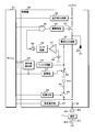
- FIG. 1 is a block diagram showing a main configuration of a power supply system 1 according to the present embodiment.
- the power supply system 1 is preferably mounted on a vehicle, and includes a battery 10, a load 11, a power supply control device 12, and outer connectors A1, A2, and A3.
- the power supply control device 12 includes a controller 20, a microcomputer (hereinafter, referred to as a microcomputer) 21, and inner connectors B1, B2, and B3.
- the positive electrode of the battery 10 is connected to the outer connector A1.
- the negative electrode of the battery 10 is grounded.
- One end of the load 11 is connected to the outer connector A2.
- the other end of the load 11 is connected to the outer connector A3.
- one end of the electric wire W is connected to the inner connector B1.
- the other end of the electric wire W is connected to the inside connector B2.
- the controller 20 is arranged in the middle of the electric wire W.
- the controller 20 is connected to the microcomputer 21.
- the inner connector B3 is grounded.
- the outer connectors A1, A2, A3 are detachably connected to the inner connectors B1, B2, B3, respectively.
- the load 11 is connected to the inner connectors B2 and B3.
- the outer connectors A1, A2, and A3 are connected to the inner connectors B1, B2, and B3, respectively, the positive electrode of the battery 10 and one end of the load 11 are connected to the controller 20, and the other end of the load 11 is grounded. You.
- the microcomputer 21 outputs a high-level voltage, a low-level voltage, or a PWM signal to the controller 20.
- the PWM signal includes a high level voltage and a low level voltage. In the PWM signal, switching from a low-level voltage to a high-level voltage or switching from a high-level voltage to a low-level voltage is performed periodically.
- the duty of the PWM signal is a ratio of a period during which the PWM signal indicates a high level voltage in one cycle. The unit of the duty of the PWM signal is percent.
- the controller 20 includes a power supply switch 30 (see FIG. 2), as described later.
- the controller 20 switches the power supply switch 30 from off to on.
- the current flows from the positive electrode of the battery 10 to the power supply switch 30 and the load 11 in this order, and power is supplied from the battery 10 to the load 11.
- the controller 20 switches the power supply switch 30 from on to off. Thereby, the power supply from the battery 10 to the load 11 is stopped.
- the controller 20 switches the power supply switch 30 from off to on. Thereby, electric power is supplied from the battery 10 to the load 11.
- the controller 20 switches the power supply switch 30 from on to off when the voltage indicated by the PWM signal switches from the high-level voltage to the low-level voltage. Thereby, the power supply from the battery 10 to the load 11 is stopped.
- the controller 20 controls the power supply from the battery 10 to the load 11 via the power supply switch 30.
- the load 11 is an electric device mounted on the vehicle.
- the load 11 operates using electric power supplied from the battery 10.
- the user disconnects the connection between the outer connector A2 and the inner connector B2 and the connection between the outer connector A3 and the inner connector B3, and replaces the outer connectors A2 and A3 connected to the new load 11 with the inner connectors. Connect to B2 and B3. Thereby, the new load 11 is connected to the inside connectors B2 and B3 of the power supply control device 12.
- FIG. 2 is a block diagram showing a main configuration of the controller 20.
- the controller 20 includes a current output circuit 31, a voltage detection circuit 32, a return diode 33, a drive circuit 34, an AND circuit 35, a variable resistor 36, a comparator 37, a DC power supply 38, a latch circuit 39, an inversion circuit, in addition to the power supply switch 30. It has a device 40, a filter circuit 41, a waveform value detection unit 42, an adjustment unit 43, a voltage dividing resistor 44, a detection switch 45, a switching unit 46, and a temperature estimation unit 47.
- the power supply switch 30 is an N-channel FET (Field Effect Transistor).
- the AND circuit 35 has two input terminals and one output terminal.
- the comparator 37 has a plus end, a minus end, and an output end.
- the inverter 40 has an input terminal and an output terminal.
- the power supply switch 30 and the current output circuit 31 are arranged in the middle of the electric wire W.
- the drain of the power supply switch 30 is connected to the inside connector B1.
- the inner connector B1 is connected to the outer connector A1, and the outer connector A1 is connected to the positive electrode of the battery 10.
- the source of the power supply switch 30 is connected to the current output circuit 31.
- the current output circuit 31 is further connected to the inside connector B2.
- the inner connector B2 is connected to the outer connector A2, and the outer connector A2 is connected to one end of the load 11.
- the voltage detection circuit 32, the cathode of the free wheel diode 33, and the microcomputer 21 are connected in the middle of the electric wire W.
- the voltage detection circuit 32 is connected to the drain of the power supply switch 30 and the microcomputer 21.
- the cathode of the return diode 33 is connected to a connection node between the source of the power supply switch 30 and the current output circuit 31.
- the anode of the return diode 33 is grounded.
- the microcomputer 21 is connected to a connection node between the current output circuit 31 and the inside connector B2.
- the gate of the power supply switch 30 is connected to the drive circuit 34.
- the drive circuit 34 is connected to the output terminal of the AND circuit 35.
- the current output circuit 31 is connected to one end of the variable resistor 36.
- the other end of the variable resistor 36 is grounded.
- a connection node between the current output circuit 31 and the variable resistor 36 is connected to the positive terminal of the comparator 37.
- the negative terminal of the comparator 37 is connected to the positive electrode of the DC power supply 38.
- the negative electrode of the DC power supply 38 is grounded.
- the output terminal of the comparator 37 is connected to the latch circuit 39.
- the latch circuit 39 is further connected to an input terminal of the inverter 40.
- One input terminal of the AND circuit 35 is connected to the microcomputer 21.
- the other input terminal of the AND circuit 35 is connected to the output terminal of the inverter 40.
- connection node between the current output circuit 31 and the variable resistor 36 is further connected to the filter circuit 41.
- the filter circuit 41 is further connected to a waveform value detector 42.
- the waveform value detector 42 is connected to the microcomputer 21.
- a resistance voltage is applied to one end of the voltage dividing resistor 44.
- the resistance voltage value Vcc which is the voltage value of the resistance voltage, is a constant value, for example, 5V.
- the other end of the voltage dividing resistor 44 is connected to one end of the detection switch 45.
- the other end of the detection switch 45 is connected to the microcomputer 21 and a connection node between the current output circuit 31 and the inside connector B2.
- the microcomputer 21 is further connected with an adjusting unit 43, a switching unit 46, and a temperature estimating unit 47.
- a connection node between the microcomputer 21 and the adjustment unit 43 is connected to the waveform value detection unit 42.
- the microcomputer 21 outputs a high-level voltage, a low-level voltage, or a PWM signal to the AND circuit 35.
- the inverter 40 outputs a high-level voltage or a low-level voltage to the AND circuit 35.
- the AND circuit 35 When the inverter 21 is outputting a high-level voltage and the microcomputer 21 is outputting a high-level voltage to the AND circuit 35, the AND circuit 35 outputs the high-level voltage to the drive circuit 34. In the same case, when the microcomputer 21 is outputting a low-level voltage to the AND circuit 35, the AND circuit 35 outputs the low-level voltage to the drive circuit 34. In the same case, when the microcomputer 21 is outputting the PWM signal to the AND circuit 35, the AND circuit 35 outputs the voltage indicated by the PWM signal to the drive circuit 34.
- the drive circuit 34 increases the gate voltage with respect to the ground potential. Thereby, in the power supply switch 30, the voltage value of the gate based on the potential of the source becomes equal to or higher than a certain voltage value, and the power supply switch 30 is turned on.
- the drive circuit 34 When the voltage output from the AND circuit 35 is switched from the high level voltage to the low level voltage, in the power supply switch 30, the drive circuit 34 lowers the gate voltage with respect to the ground potential. Thereby, in the power supply switch 30, the voltage value of the gate based on the potential of the source becomes less than a certain voltage value, and the power supply switch 30 is turned off.
- the drive circuit 34 functions as a switching unit.
- the drive circuit 34 switches the power supply switch 30 on, the current flows from the positive electrode of the battery 10 to the outer connector A1, the inner connector B1, the power switch 30, the current output circuit 31, the inner connector B2, the outer connector A2, the load 11, The power flows through the outer connector A3 and the inner connector B3 in this order, and power is supplied to the load 11. Therefore, the inner connectors B2 and B3 are arranged on the current path of the current flowing through the power supply switch 30.
- the drive circuit 34 switches off the power supply switch 30, power supply from the battery 10 to the load 11 is stopped.
- load 11 is an inductive load having a coil.
- energy is accumulated in the coil of the load 11.
- the power supply switch 30 is turned off, a current flows from one end of the load 11 on the side of the outer connector A3 to the return diode 33, the current output circuit 31, and the load 11 in this order, and the coil of the load 11 emits energy.
- the reflux diode 33 is a diode for releasing the energy of the load 11. When the load 11 is not an inductive load, no current flows through the free wheel diode 33.
- the battery voltage value is a voltage value of the voltage applied to the load 11 when the power supply switch 30 is on when the load 11 is connected to the inner connectors B2 and B3.
- the voltage detection circuit 32 detects a battery voltage value.
- the voltage detection circuit 32 outputs analog voltage information indicating the detected battery voltage value to the microcomputer 21.
- the voltage detection circuit 32 has two resistors. In this case, the two resistors divide the voltage of the battery 10 and output the voltage value of the divided voltage to the microcomputer 21 as voltage information.
- the current output circuit 31 is configured using, for example, a current mirror circuit, and outputs a current to the variable resistor 36.
- the current value of the current output from the current output circuit 31 to the variable resistor 36 is a value calculated by dividing the load current value by a predetermined number.
- the load current value, the predetermined number, and the variable resistance value of the variable resistor 36 are respectively described as Ic, N, and Rv.
- the voltage value between both ends of the variable resistor 36 is represented by Ic ⁇ Rv / N. “ ⁇ ” Represents a product.
- a voltage value between both ends of the variable resistor 36 is referred to as a voltage value between both ends.
- the power supply voltage value which is the positive voltage value of the DC power supply 38 with respect to the ground potential, is described as Vd.
- the comparator 37 When Ic ⁇ Rv / N ⁇ Vd is satisfied, that is, when Ic ⁇ N ⁇ Vd / Rv is satisfied, the comparator 37 outputs a high-level voltage to the latch circuit 39.
- the current threshold value Ith of the load current value Ic is represented by N ⁇ Vd / Rv.
- the predetermined number N and the power supply voltage value Vd are constant values. Therefore, the current threshold value Ith changes according to the variable resistance value Rv.
- the current threshold value Ith is smaller as the variable resistance value Rv is larger.
- the microcomputer 21 outputs a resistance value signal indicating a resistance value to the waveform value detection unit 42 and the adjustment unit 43.
- the adjustment unit 43 adjusts the variable resistance value of the variable resistor to the resistance value indicated by the input resistance value signal. Therefore, the variable resistance value, that is, the current threshold value is adjusted by the microcomputer 21.
- the waveform value detection unit 42 is notified of the variable resistance value.
- the latch circuit 39 outputs the low-level voltage to the inverter 40 while the comparator 37 outputs the low-level voltage, that is, while the load current value is less than the current threshold.
- the inverter 40 outputs a high-level voltage when the latch circuit 39 outputs a low-level voltage.
- the AND circuit 35 outputs the voltage output by the microcomputer 21 or the voltage indicated by the PWM signal to the drive circuit 34, and the drive circuit 34
- the power supply switch 30 is turned on or off in accordance with an instruction from the microcomputer 21.
- the latch circuit 39 When the voltage output to the comparator 37 switches from the low-level voltage to the high-level voltage, that is, when the load current value becomes equal to or more than the current threshold, the latch circuit 39 outputs the voltage output to the inverter 40. Switch from the low level voltage to the high level voltage. Thus, the inverter 40 switches the voltage output to the AND circuit 35 from the high level voltage to the low level voltage. When the voltage output from the inverter 40 is switched from the high level voltage to the low level voltage, the voltage output from the AND circuit 35 is switched from the high level voltage to the low level voltage, and the driving circuit 34 The power supply switch 30 is turned off irrespective of the output from 21 to the AND circuit 35.
- the latch circuit 39 After switching the voltage output to the inverter 40 to the high level voltage, the latch circuit 39 continues to output the high level voltage to the inverter 40 irrespective of the voltage output from the comparator 37. Therefore, after the load current value becomes equal to or larger than the current threshold, the drive circuit 34 keeps the power supply switch 30 off.
- the voltage value at both ends of the variable resistor 36 is input to the filter circuit 41.
- the filter circuit 41 removes noise from the input analog voltage value at both ends.
- the filter circuit 41 outputs to the waveform value detection unit 42 the analog voltage value between both ends from which noise has been removed.
- the filter circuit 41 is configured using, for example, a resistor and a capacitor.
- the waveform value detection unit 42 periodically converts an analog voltage value between both ends into a digital voltage value between both ends, and acquires the converted digital voltage value between both ends.
- the microcomputer 21 notifies the waveform value detection unit 42 of the variable resistance value Rv.
- the waveform value detection unit 42 detects and detects a plurality of waveform values related to the current waveform drawn by the load current value Ic based on the plurality of voltage values Vb at both ends periodically acquired, that is, the plurality of load current values Ic.
- the microcomputer 21 notifies the microcomputer 21 of a plurality of waveform values.
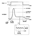
- FIG. 3 is an explanatory diagram of a plurality of waveform values.
- FIG. 3 shows the transition of the power supply switch 30 on and off, and the transition of the load current value.
- the horizontal axis of these transitions represents time.
- the load 11 has a resistance component. Therefore, when a current flows through the load 11, the temperature of the load 11 increases, and when the current supply to the load 11 is stopped, the temperature of the load 11 decreases. Assume that the temperature of the load 11 is low.
- the power supply switch 30 is switched from off to on, as shown in FIG. 3, the load current value rapidly increases from zero A, and then rapidly decreases.
- the current whose current value rises rapidly and falls rapidly is an inrush current.
- the rising speed of the load current value related to the inrush current is one waveform value.
- the peak value of the load current value related to the inrush current is the inrush current value.
- the time from when the power supply switch 30 is switched from off to on until the load current value reaches (1- (1 / e)) ( 0.632) times (e: natural logarithm) of the inrush current value. It is the time constant of the inrush current.
- the load current value stabilizes over time.
- the average value of the stable load current values is the steady-state current value.
- the load current value oscillates finely. This oscillation width is a ripple current value.
- the cycle related to this oscillation is the ripple current cycle.
- the inrush current value, the time constant of the inrush current, the steady current value, the ripple current value, and the ripple current cycle are each one waveform value.
- the waveform value detection unit 42 calculates the steady-state current value, the inrush current value, the time constant of the inrush current, the number of inrush currents, the rising speed of the inrush current, the ripple current value, the ripple current cycle, and the reflux time as a plurality of waveform values. Output to These values are digital values.
- the waveform value detection unit 42 also outputs a digital load current value to the microcomputer 21.
- the voltage value of the inner connector B2 based on the ground potential is input to the microcomputer 21.
- the voltage value of the inner connector B2 based on the ground potential is referred to as a connector voltage value.
- An analog connector voltage value is input to the microcomputer 21.
- the microcomputer 21 detects the connection of the load 11 to the inner connectors B2 and B3 based on the connector voltage values when the power supply switch 30 and the detection switch 45 are off and on, respectively.
- the resistance value of the voltage dividing resistor 44 is sufficiently larger than the resistance value of the load 11 that may be connected to the inner connectors B2 and B3.
- the connector voltage value is sufficiently lower than the resistance voltage value Vcc and less than the reference voltage value.
- the reference voltage value is a constant value and is set in advance.
- the temperature estimating unit 47 estimates the environmental temperature that is the ambient temperature of the load 11 and outputs analog temperature information indicating the estimated environmental temperature to the microcomputer 21.
- the temperature estimating unit 47 outputs, for example, an analog voltage value corresponding to the estimated environmental temperature to the microcomputer 21 as analog temperature information.
- the environmental temperature estimated by the temperature estimating unit 47 is the environmental temperature in the vehicle, and corresponds to not only the ambient temperature of the load 11 but also, for example, the ambient temperature of the electric wire W.
- FIG. 4 is a block diagram showing a main configuration of the microcomputer 21.
- the microcomputer 21 has input units 50, 51, 52, 53, output units 54, 55, 56, A / D conversion units 57, 58, 59, a timer 60, a storage unit 61, and a control unit 62.
- the input units 50, 51, 52 are respectively connected to A / D conversion units 57, 58, 59.
- the input unit 53, the output units 54, 55, 56, the A / D conversion units 57, 58, 59, the timer 60, the storage unit 61, and the control unit 62 are connected to the internal bus 63.
- the input unit 50 is further connected to the voltage detection circuit 32.
- the input unit 51 is further connected to the middle of the electric wire W.
- the input unit 52 is further connected to the temperature estimating unit 47.
- the input unit 53 is further connected to the waveform value detection unit 42.
- the output unit 54 is further connected to one input terminal of the AND circuit 35.
- the output unit 55 is further connected to the waveform value detection unit 42 and the adjustment unit 43.
- the output unit 56 is further connected to the switching unit 46.
- Analog voltage information is input from the voltage detection circuit 32 to the input unit 50.
- the input unit 50 outputs the analog voltage information input from the voltage detection circuit 32 to the A / D conversion unit 57.
- the A / D converter 57 converts analog voltage information input from the input unit 50 into digital voltage information.
- the control unit 62 acquires digital voltage information from the A / D conversion unit 57.
- the output unit 54 outputs a high-level voltage, a low-level voltage, or a PWM signal to the AND circuit 35 according to an instruction from the control unit 62.
- the control unit 62 also instructs the output unit 54 on the duty of the PWM signal.
- the waveform value detection unit 42 inputs the steady current value, the inrush current value, the time constant of the inrush current, the number of inrush currents, the rising speed of the inrush current, the ripple current value, the ripple current cycle, and the reflux time as a plurality of waveform values. Output to 53.
- the control unit 62 acquires these waveform values from the input unit 53.
- the waveform value detection unit 42 also outputs the load current value to the input unit 53, and the control unit 62 acquires the load current value from the input unit 53.
- the output unit 55 outputs a resistance value signal indicating a resistance value to the waveform value detection unit 42 and the adjustment unit 43 according to an instruction from the control unit 62.
- the adjustment unit 43 adjusts the variable resistance value of the variable resistor 36 to the resistance value of the resistance signal, and notifies the waveform value detection unit 42 of the variable resistance value.
- the output unit 56 outputs an ON signal and an OFF signal to the switching unit 46 according to an instruction from the control unit 62.
- the switching unit 46 switches the detection switch 45 on when an ON signal is input, and switches off the detection switch 45 when an OFF signal is input.
- An analog connector voltage value is input to the input unit 51.
- the input unit 51 outputs the input analog connector voltage value to the A / D conversion unit 58.
- the A / D converter 58 converts an analog connector voltage value input from the input unit 51 into a digital connector voltage value.
- the control section 62 acquires a digital connector voltage value from the A / D conversion section 58.
- Analog temperature information is input from the temperature estimating unit 47 to the input unit 52.
- the input unit 52 outputs the analog temperature information input from the temperature estimation unit 47 to the A / D conversion unit 59.
- the A / D converter 57 converts the analog temperature information input from the input unit 52 into digital temperature information.
- the control unit 62 acquires digital voltage information from the A / D conversion unit 59.
- the timer 60 starts and ends timing according to an instruction from the control unit 62.
- the time measured by the timer 60 is read from the timer 60 by the control unit 62.
- the storage unit 61 is a nonvolatile memory.
- the storage unit 61 stores a computer program 70, a power supply control table 71, and a waveform value table 72.
- the control unit 62 has a processing element that executes processing.
- the processing element is, for example, a CPU (Central Processing Unit).
- the processing elements included in the control unit 62 execute the computer program 70 to control the power supply to the load 11, the electric wire protection processing to protect the electric wire W from abnormal temperature, and to the inner connectors B2 and B3. And a connection detection process for detecting the connection of the load 11 of the connection.
- the computer program 70 is used for causing a processing element (computer) of the control unit 62 to execute a power supply control process, a wire protection process, and a connection detection process.
- the number of processing elements included in the control unit 62 may be two or more. In this case, a plurality of processing elements may cooperatively execute the power supply control processing, the electric wire protection processing, and the connection detection processing.
- the computer program 70 may be stored in the storage medium E so that the processing element of the control unit 62 can read the computer program 70.
- the computer program 70 read from the storage medium E by a reading device (not shown) is stored in the storage unit 61.
- the storage medium E is an optical disk, a flexible disk, a magnetic disk, a magnetic optical disk, a semiconductor memory, or the like.
- the optical disk is a CD (Compact Disc) -ROM (Read Only Memory), a DVD (Digital Versatile Disc) -ROM, or a BD (Blu-ray (registered trademark) Disc).
- the magnetic disk is, for example, a hard disk.
- the computer program 70 may be downloaded from an external device (not shown) connected to a communication network (not shown), and the downloaded computer program 70 may be stored in the storage unit 61.
- FIG. 5 is a chart showing the power supply control table 71.
- the power supply control table 71 includes a power supply flag field, a connection flag field, a type field, a variable resistance field, a current threshold field, a PWM flag field, a duty field, a prohibition flag field, a preceding temperature difference field, and a temperature threshold field. .
- the value of the power supply flag is stored in the power supply flag field.
- the value of the power supply flag is set to zero or one by the control unit 62.
- the fact that the value of the power supply flag is zero means that the power supply switch 30 is off and power is not being supplied to the load 11.
- the fact that the value of the power supply flag is 1 means that the power supply switch 30 is on and power is being supplied to the load 11.
- connection flag is stored in the connection flag field.
- the value of the connection flag is set to zero or one by the control unit 62.
- the fact that the value of the connection flag is zero means that the load 11 is not connected to the inner connectors B2 and B3.
- the value of the connection flag is 1, it means that the load 11 is connected to the inner connectors B2 and B3.
- the type of the load 11 is stored in the type field. Examples of the type of the load 11 include a valve, a motor with a brush, and a magnetic clutch.
- the type of the load 11 is updated by the control unit 62.
- the variable resistance value field stores the variable resistance value of the variable resistor 36.
- the variable resistance value stored in the variable resistance value field is updated by the control unit 62.
- the current threshold field is stored in the current threshold field.
- the current threshold stored in the current threshold field is updated by the control unit 62.
- the current threshold value Ith is represented by N ⁇ Vd / Rv.
- N, Vd, and Rv are a predetermined number, a power supply voltage value, and a variable resistance value, respectively. Since the predetermined number N and the power supply voltage value Vd are constants, determining the current threshold value Ith is equivalent to determining the variable resistance value Rv.
- the value of the PWM flag is stored in the PWM flag field.
- the value of the PWM flag is set to zero or one by the control unit 62. When the value of the PWM flag is zero, it means that the PWM control is not performed for turning on and off the power supply switch 30. The fact that the value of the PWM flag is 1 means that PWM control is performed on and off of the power supply switch 30.
- the duty field stores the duty value of the PWM signal. The duty value is updated by the control unit 62.
- the value of the prohibition flag is stored in the prohibition flag field.
- the value of the prohibition flag is set to zero or one by the control unit 62. When the value of the prohibition flag is zero, it means that power supply via the electric wire W is permitted. The fact that the value of the prohibition flag is 1 means that power supply via the electric wire W is prohibited.
- the control unit 62 repeatedly executes the wire protection processing.
- the control unit 62 repeatedly calculates the temperature difference between the environmental temperature and the temperature of the electric wire W.
- the temperature of the electric wire W is referred to as the electric wire temperature.
- the preceding temperature difference field a temperature difference previously calculated by the control unit 62 is stored.
- the preceding temperature difference is updated by the control unit 62.
- the temperature threshold field a temperature threshold related to wire protection is stored.
- the electric wire temperature is prevented from exceeding the temperature threshold.
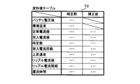
- FIG. 6 is a chart showing a waveform value table.
- the control unit 62 converts each waveform value input from the waveform value detection unit 42 to the input unit 53 into a waveform when the battery voltage value is a predetermined voltage value and the environmental temperature is a predetermined temperature. Correct to value.
- the predetermined voltage value is, for example, 12V.
- the waveform value table includes a battery voltage value field, an environmental temperature field, a steady current value field, an inrush current value field, a time constant field, an inrush current frequency field, a rising speed field, a ripple current value field, a ripple current cycle field, and a reflux time. Fields are provided.
- the battery voltage value field stores a battery voltage value.
- the controller 62 updates the battery voltage value in the battery voltage value field. As described above, the control unit 62 acquires the voltage information indicating the battery voltage value from the A / D conversion unit 57.
- the environmental temperature field stores an environmental temperature. The environmental temperature in the environmental temperature field is updated by the control unit 62. As described above, the control unit 62 acquires temperature information indicating the environmental temperature from the A / D conversion unit 57.
- An inrush current value, a time constant, the number of inrush currents, a rising speed, a ripple current value, a ripple current cycle, and a reflux time are stored.
- the values before and after the correction in these fields are updated by the control unit 62.
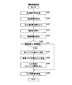
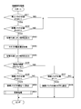
- FIG. 7 is a flowchart showing the procedure of the power supply control process.
- the control unit 62 periodically executes a power supply control process.
- the inverter 40 outputs a high-level voltage, that is, the load current value is less than the current threshold.
- the drive circuit 34 keeps the power supply switch 30 off regardless of the output of the output unit 54.
- the control unit 62 determines whether or not the value of the prohibition flag in the power supply control table 71 is zero (Step S1). If the control unit 62 determines that the value of the prohibition flag is zero, that is, that power supply via the electric wire W is permitted (S1: YES), the control unit 62 determines whether the value of the connection flag is one. (Step S2).
- the control unit 62 determines that the value of the prohibition flag is not zero, that is, the value of the prohibition flag is 1 (S1: NO), or that the value of the connection flag is not 1, that is, If it is determined that the value is zero (S2: NO), the power supply control process ends.
- the fact that the value of the prohibition flag is 1 means that power supply via the electric wire W is prohibited.
- the fact that the value of the connection flag is zero means that the load 11 is not connected to the inner connectors B2 and B3.
- step S3 When the value of the connection flag is 1, that is, when the control unit 62 determines that the load 11 is connected to the inner connectors B2 and B3 (S2: YES), the control unit 62 determines whether to start power supply to the load 11. Is determined (step S3).
- step S3 for example, when a start signal instructing the start of power supply is input to an input unit (not shown), the control unit 62 determines that power supply is to be started, and when the start signal is not input to the input unit, It is determined that power supply is not started.
- step S4 determines whether or not to terminate the power supply to the load 11 (step S4).
- step S4 for example, when an end signal instructing the end of power supply is input to an input unit (not shown), the control unit 62 determines that power supply is to be ended, and when the end signal is not input to the input unit, It is determined that the power supply is not terminated.
- the control unit 62 terminates the power supply control process.
- the control unit 62 When determining that power supply is to be terminated (S4: YES), the control unit 62 sets the value of the power supply flag in the power supply control table 71 to zero (step S5), instructs the output unit 54 to output a low-level signal to the AND circuit 35, A voltage is output (step S6). As a result, the AND circuit 35 outputs a low-level voltage to the drive circuit 34, and the drive circuit 34 switches off the power supply switch 30. Instructing the output unit 54 to output a low-level voltage is equivalent to instructing the drive circuit 34 to switch on the power supply switch 30. After executing Step S6, the control unit 62 ends the power supply control process.
- the control unit 62 sets the value of the power supply flag in the power supply control table 71 to 1 (step S7), instructs the output unit 55 to change the resistance value to the power supply control.
- a resistance value signal which is a variable resistance value of the table 71, is output (step S8).
- the adjusting unit 43 adjusts the variable resistance value of the variable resistor 36 to the variable resistance value shown in the power supply control table 71.
- the current threshold is changed to the current threshold indicated in the power supply control table 71.
- the variable resistance value of the power supply control table 71 is notified to the waveform value detection unit 42.
- step S8 the control unit 62 determines whether the value of the PWM flag in the power supply control table 71 is zero (step S9).
- the control unit 62 instructs the output unit 54 to output the high-level voltage to the AND circuit 35 (S9: YES).
- Step S10 the voltage output from the AND circuit 35 to the drive circuit 34 is switched to the high-level voltage, and the drive circuit 34 switches on the power supply switch 30.
- power is supplied to the load 11. Instructing the output unit 54 to output a high-level voltage is equivalent to instructing the drive circuit 34 to switch on the power supply switch 30.
- the control unit 62 determines that the value of the PWM flag is not zero, that is, the value of the PWM flag is 1 (S9: NO)
- the control unit 62 instructs the output unit 54 to output the PWM signal to the AND circuit 35.
- the AND circuit 35 outputs the voltage indicated by the PWM signal to the drive circuit 34, and the drive circuit 34 alternately switches the power supply switch 30 on and off in accordance with the voltage indicated by the PWM signal.
- power is supplied to the load 11.
- the duty of the PWM signal is adjusted to the duty stored in the power supply control table 71.
- Instructing the output unit 54 to output a PWM signal is equivalent to instructing the drive circuit 34 to alternately switch the power supply switch 30 on and off.
- the fact that the value of the PWM flag is 1 means that the PWM control is performed.
- the control unit 62 of the microcomputer 21 performs power supply control according to the power supply control conditions shown in the power supply control table 71.
- the power supply control condition is a condition related to power supply control to the load 11, and specifically includes a variable resistance value (current threshold), a value of a PWM flag, and a duty of a PWM signal.
- the power supply control condition is appropriately changed in the connection detection process.
- FIG. 8 is a flowchart showing the procedure of the electric wire protection processing.
- the control unit 62 periodically executes the electric wire protection processing.
- the control unit 62 first obtains a load current value from the input unit 53 (step S21), and obtains temperature information from the A / D conversion unit 57 (step S22).
- the control unit 62 reads the preceding temperature difference stored in the power supply control table 71 (Step S23).
- control unit 62 determines the electric wire temperature of the electric wire W based on the load current value acquired in step S21, the environmental temperature indicated by the temperature information acquired in step S22, and the preceding temperature difference read in step S23. Then, a temperature difference from the environmental temperature in the vehicle is calculated (step S24). The preceding temperature difference read in step S23 is the temperature difference calculated in the previous wire protection processing. Next, the control unit 62 calculates the electric wire temperature by adding the environmental temperature obtained in step S22 to the temperature difference calculated in step S24 (step S25).
- the controller 62 determines whether or not the electric wire temperature calculated in step S25 is equal to or higher than the temperature threshold in the power supply control table 71 (step S26).
- the control unit 62 sets the value of the prohibition flag to 1 (Step S27), and sets the value of the power supply flag to zero (Step S28).
- the output unit 54 to output a low-level voltage to the AND circuit 35 (step S29).
- the AND circuit 35 switches the voltage output to the drive circuit 34 to the low level voltage, and the drive circuit 34 switches the power supply switch 30 off.
- the power supply to the load 11 stops.
- the value of the prohibition flag is set to 1, so that the power supply switch 30 is not switched on in the power supply control process.
- step S30 the control unit 62 compares the preceding temperature difference in the power supply control table 71 with the temperature difference calculated in step S24. Update (step S30), and end the wire protection process.
- the drive circuit 34 switches off the power supply switch 30 and keeps the power supply switch 30 off. Therefore, the wire temperature does not exceed the temperature threshold.
- the preceding temperature difference is not limited to the temperature difference calculated in the previous electric wire protection process, since the preceding temperature difference may be any temperature difference calculated in advance.
- the preceding temperature difference may be a temperature difference calculated in the electric wire protection process two times before.
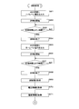
- FIG. 9 is a flowchart showing the procedure of the connection detection process.
- the control unit 62 periodically executes the connection detection process.
- the control unit 62 determines whether or not the value of the prohibition flag in the power supply control table 71 is zero (step S41).
- the control unit 62 determines whether the value of the power supply flag is zero. (Step S42).
- the connection detection process ends. Therefore, when the power supply to the load 11 is prohibited or when the power supply switch 30 is turned on, the connection detection processing ends.
- the control unit 62 determines that the value of the power supply flag is zero, that is, the power supply switch 30 is off (S42: YES)
- the control unit 62 instructs the output unit 55 to output an on signal to the switching unit 46.
- Step S43 the switching unit 46 switches the detection switch 45 on, and the voltage value of the voltage divided by the voltage dividing resistor 44 and the load 11 is output to the input unit 51 as an analog connector voltage value.
- the analog connector voltage value input to the input unit 51 is converted by the A / D converter 58 into a digital connector voltage value.
- control unit 62 After executing step S43, the control unit 62 acquires the connector voltage value from the A / D conversion unit 58 (step S44), instructs the output unit 56 to output the OFF signal to the switching unit 46 (step S45). ). Thereby, the switching unit 46 switches the detection switch 45 off.
- step S46 determines whether or not the load 11 is connected to the inside connectors B2 and B3 based on the connector voltage value acquired in step S44 (step S46).
- step S46 when the connector voltage value is lower than the reference voltage value, the control unit 62 determines that the load 11 is connected.
- the control unit 62 determines that the load 11 is not connected.
- the control unit 62 detects the connection of the load 11 to the inside connectors B2 and B3 by executing step S46.
- the control unit 62 functions as a connection detection unit.
- control unit 62 determines whether the value of the connection flag in the power supply control table 71 is 1 (step S47).
- the fact that the value of the connection flag is 1 means that the load 11 was connected when the previous connection detection processing was completed.
- control unit 62 determines that the value of the connection flag is not 1, that is, the value of the connection flag is zero (S47: NO)
- the control unit 62 ends the connection detection process.
- the control unit 62 sets the value of the connection flag to zero (Step S48), and ends the connection detection process.
- the control unit 62 determines whether the value of the connection flag in the power supply control table 71 is zero. A determination is made (step S49).
- the fact that the value of the connection flag is zero means that the load 11 was not connected at the time when the previous connection detection processing was completed.
- control unit 62 determines that the value of the connection flag is not zero, that is, the value of the connection flag is 1 (S49: NO)
- the control unit 62 ends the connection detection process.
- the control unit 62 sets the value of the connection flag to 1 (step S50), and sets the plurality of waveform values stored in the waveform value table 72.
- An update process for updating is performed (step S51), and the connection detection process ends.
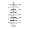
- FIGS. 10 and 11 are flowcharts showing the procedure of the update process.
- the inverter 40 outputs a high-level voltage, that is, the load current value is less than the current threshold.
- the driving circuit 34 keeps the power supply switch 30 off regardless of the output of the output unit 54.
- control unit 62 first instructs the output unit 54 to output a high-level voltage to the AND circuit 35 (step S61).
- the AND circuit 35 outputs a high-level voltage to the drive circuit 34, the drive circuit 34 switches the power supply switch 30 from off to on, and current flows from the battery 10 to the load 11.
- the control unit 62 instructs the timer 60 to start time measurement (step S62), and determines whether the time measured by the timer 60 is equal to or longer than the ON time (step S63).
- the ON time is a constant value and is set in advance.
- the control unit 62 executes step S63 again, and waits until the time reaches the ON time.
- the control unit 62 determines that the counted time is equal to or longer than the ON time (S63: YES)
- the control unit 62 instructs the timer 60 to end the counting (step S64).
- control unit 62 instructs the output unit 54 to output a low-level voltage to the AND circuit 35 (step S65).
- the AND circuit 35 outputs a low-level voltage to the drive circuit 34
- the drive circuit 34 switches the power supply switch 30 from on to off, and power supply from the battery 10 to the load 11 is stopped.
- the control unit 62 instructs the timer 60 to start time measurement again (step S66), and determines whether the time measured by the timer 60 is equal to or longer than the off time (step S67). ).
- the off time is also a constant value and is set in advance.
- the control unit 62 determines that the time is less than the off time (S67: NO)
- the control unit 62 executes step S67 again and waits until the time reaches the off time.
- the control unit 62 determines that the counted time is equal to or longer than the off time (S67: YES)
- the control unit 62 instructs the timer 60 to end the counting (step S68).
- the power supply switch 30 is kept on until the on-time elapses from the start of the update processing, and thereafter, the power supply switch 30 is kept off until the off-time elapses.
- the load current value draws a current waveform as shown in FIG.
- the waveform value detection unit 42 detects a plurality of waveform values and outputs the detected plurality of waveform values to the input unit 53.
- the control unit 62 acquires a plurality of waveform values from the input unit 53 (step S69).
- the plurality of waveform values acquired in step S69 are a steady current value, an inrush current value, a time constant of the inrush current, the number of inrush currents, a rising speed of the inrush current, a ripple current value, a ripple current cycle, and a reflux time.
- the control unit 62 acquires voltage information from the A / D conversion unit 57 (step S70), and acquires temperature information from the A / D conversion unit 59 (step S71).
- the control unit 62 updates the plurality of waveform values, the battery voltage value, and the environmental temperature of the power supply control table 71 before correction (step S72).
- control unit 62 updates the plurality of waveform values before correction with the plurality of waveform values acquired in step S69.
- the control unit 62 updates the battery voltage value in the power supply control table 71 to the battery voltage value indicated by the voltage information acquired in step S70, and sets the environmental temperature in the power supply control table 71 to the environment indicated by the temperature information acquired in step S71. Update to temperature.
- control unit 62 determines a plurality of waveform values before correction in the waveform value table 72 based on the battery voltage value and the environmental temperature stored in the waveform value table 72, and determines whether the battery voltage value is a predetermined voltage value.
- the correction is made to a plurality of waveform values when the environmental temperature is the predetermined temperature (step S73).
- the control unit 62 also functions as a correction unit and a second correction unit.
- the control unit 62 updates the plurality of corrected waveform values in the waveform value table 72 to the plurality of waveform values corrected in step S73 (step S74).
- the control unit 62 specifies the type of the load 11 based on the plurality of corrected waveform values in the waveform value table 72 (step S75).
- the control unit 62 calculates a correlation value between the plurality of waveform values corresponding to each type and the plurality of corrected waveform values according to the waveform value table 72.
- the control unit 62 specifies the type of the load 11 to be the type having the highest similarity indicated by the calculated correlation value among the plurality of types described above.
- the type of the load 11 is specified using a learning model that has learned the relationship between a plurality of waveform values and the type of the load 11.
- the learning model is configured by, for example, a neutral network, and is configured by an input layer, a plurality of intermediate layers, and an output layer. Each layer node is connected to an adjacent layer node.
- the learning model learns the relationship between the plurality of waveform values and the type of load 11 in advance.
- the control unit 62 inputs the waveform value data indicating a plurality of corrected waveform values in the waveform value table 72 to the input layer of the learning model, and based on the output value output from the output layer of the learning model.
- the type of the load 11 is specified.
- the output value of the output layer indicates a probability corresponding to the type of the actual load 11 for each of the plurality of types.
- the control unit 62 also functions as a specifying unit.
- the type of the load 11 stored in the power supply control table 71 is updated to the type specified in step S75 (step S76).
- the control unit 62 determines power supply control conditions based on the type in the power supply control table 71 and the plurality of corrected waveform values in the waveform value table 72 (step S77).
- the power supply control condition includes a variable resistance value, a current threshold value, a value of a PWM flag, and a duty of a PWM signal.
- the control unit 62 also functions as a determination unit. For example, the condition regarding power supply control is stored in the storage unit 61 in advance for each of the plurality of types of the load 11.
- the control unit 62 determines the power supply control condition to be a condition corresponding to the type of the load 11 specified in step S75.
- N and Vd are a predetermined number and a power supply voltage value, respectively, and are constant values. Determining the value of the PWM flag is equivalent to determining whether to perform PWM control on and off of the power supply switch 30.
- control unit 62 updates the power supply control condition in the power supply control table 71 to the power supply control condition determined in step S77 (step S78). After executing the step S78, the control unit 62 ends the updating process, and returns the process to the connection detecting process. As described above, when the control unit 62 ends the update process, the control unit 62 also ends the connection detection process.
- the control unit 62 detects this connection and executes the update process.
- the control unit 62 causes the drive circuit 34 to switch the power supply switch 30 from off to on, and then causes the drive circuit 34 to switch the power supply switch 30 from on to off.
- the control unit 62 determines the power supply control condition and updates the power supply control condition in the power supply control table 71.
- the plurality of waveform values used for determining the power supply control conditions that is, the plurality of waveform values stored in the waveform value table 72 include a steady current value, an inrush current value, a time constant of the inrush current, the number of inrush current, and a load. It is not limited to the rising speed of the current value, the ripple current value, the ripple current cycle, and the reflux time. Further, the plurality of waveform values include all of a steady current value, an inrush current value, a time constant of the inrush current, the number of inrush currents, a rising speed of the load current value, a ripple current value, a ripple current cycle, and a reflux time. It is not necessary. Further, the number of waveform values is not limited to 7, and may be any of 1 to 6, or 8 or more.
- the items included in the power supply control conditions are not limited to the variable resistance value, the current threshold value, the value of the PWM flag, and the duty.
- a temperature threshold may be included as an item of the power supply control condition.
- the control unit 62 of the microcomputer 21 may estimate the ambient temperature, which is the ambient temperature of the load 11, based on the values of various parameters related to the load 11.
- the power supply switch 30 is not limited to an N-channel FET, but may be a P-channel FET, a bipolar transistor, a relay contact, or the like.
Landscapes
- Engineering & Computer Science (AREA)
- Power Engineering (AREA)
- Dc-Dc Converters (AREA)
- Remote Monitoring And Control Of Power-Distribution Networks (AREA)
- Direct Current Feeding And Distribution (AREA)
Priority Applications (2)
| Application Number | Priority Date | Filing Date | Title |
|---|---|---|---|
| US17/270,619 US11699952B2 (en) | 2018-08-30 | 2019-08-23 | Power supply control device, power supply control method, and computer program |
| CN201980052785.8A CN112567582B (zh) | 2018-08-30 | 2019-08-23 | 供电控制装置、供电控制方法及计算机程序 |
Applications Claiming Priority (2)
| Application Number | Priority Date | Filing Date | Title |
|---|---|---|---|
| JP2018161492A JP7167559B2 (ja) | 2018-08-30 | 2018-08-30 | 給電制御装置、給電制御方法及びコンピュータプログラム |
| JP2018-161492 | 2018-08-30 |
Publications (1)
| Publication Number | Publication Date |
|---|---|
| WO2020045305A1 true WO2020045305A1 (ja) | 2020-03-05 |
Family
ID=69644283
Family Applications (1)
| Application Number | Title | Priority Date | Filing Date |
|---|---|---|---|
| PCT/JP2019/033131 Ceased WO2020045305A1 (ja) | 2018-08-30 | 2019-08-23 | 給電制御装置、給電制御方法及びコンピュータプログラム |
Country Status (4)
| Country | Link |
|---|---|
| US (1) | US11699952B2 (https=) |
| JP (1) | JP7167559B2 (https=) |
| CN (1) | CN112567582B (https=) |
| WO (1) | WO2020045305A1 (https=) |
Families Citing this family (4)
| Publication number | Priority date | Publication date | Assignee | Title |
|---|---|---|---|---|
| JP7567365B2 (ja) * | 2020-10-28 | 2024-10-16 | 株式会社オートネットワーク技術研究所 | 給電制御装置、車載制御装置及び給電制御方法 |
| US20250018797A1 (en) * | 2021-04-21 | 2025-01-16 | Autonetworks Technologies, Ltd. | Vehicle-mounted control device |
| IT202100023351A1 (it) * | 2021-09-09 | 2023-03-09 | St Microelectronics Srl | Chip di base del sistema, sistema di elaborazione, dispositivo e procedimento corrispondenti |
| CN117032038A (zh) * | 2023-08-30 | 2023-11-10 | 浙江杰创电器有限公司 | 一种四合一集成模块电源控制系统 |
Citations (3)
| Publication number | Priority date | Publication date | Assignee | Title |
|---|---|---|---|---|
| JP2008290705A (ja) * | 2007-02-28 | 2008-12-04 | Stmicroelectronics Inc | 電気装置及び短絡回路保護の分類用の集積回路及び方法 |
| US20090080130A1 (en) * | 2007-09-26 | 2009-03-26 | Lear Corporation | Automotive overcurrent protection |
| JP2019097124A (ja) * | 2017-11-27 | 2019-06-20 | アンデン株式会社 | 負荷駆動回路 |
Family Cites Families (15)
| Publication number | Priority date | Publication date | Assignee | Title |
|---|---|---|---|---|
| GB0610422D0 (en) * | 2006-05-26 | 2006-07-05 | Cambridge Semiconductor Ltd | Forward power converters |
| JP2008306809A (ja) | 2007-06-06 | 2008-12-18 | Konica Minolta Holdings Inc | 電力供給装置、電源管理システム |
| WO2013033247A1 (en) | 2011-08-29 | 2013-03-07 | Control4 Corporation | Wall box device for managing energy |
| TWI560980B (en) * | 2012-09-27 | 2016-12-01 | Joint Power Exponent Ltd | A switch control system |
| JP5749238B2 (ja) | 2012-11-09 | 2015-07-15 | 古河電気工業株式会社 | 車両用ランプ制御ユニット |
| GB201309282D0 (en) * | 2013-05-23 | 2013-07-10 | Shimadzu Corp | Circuit for generating a voltage waveform |
| JP2015056857A (ja) * | 2013-09-13 | 2015-03-23 | 株式会社オートネットワーク技術研究所 | 制御システム |
| JP2016027365A (ja) * | 2014-06-23 | 2016-02-18 | セイコーエプソン株式会社 | 集積回路装置及び電子機器、並びに、電気光学パネルの制御方法 |
| JP6353746B2 (ja) | 2014-08-26 | 2018-07-04 | 矢崎総業株式会社 | 車両用電源制御システム、ワイヤハーネス及び車両用電源制御装置 |
| JP6394535B2 (ja) * | 2015-08-20 | 2018-09-26 | 株式会社オートネットワーク技術研究所 | 電線保護装置 |
| JP6365497B2 (ja) * | 2015-10-14 | 2018-08-01 | 株式会社オートネットワーク技術研究所 | 電流制御装置、電流制御方法及びコンピュータプログラム |
| JP2017182799A (ja) * | 2016-03-25 | 2017-10-05 | 古河電気工業株式会社 | 電源供給装置 |
| US10128740B1 (en) * | 2016-09-06 | 2018-11-13 | Universal Lighting Technologies | Dynamic AC impedance stabilization in a flyback LED driver |
| CN108063426A (zh) * | 2016-11-09 | 2018-05-22 | 株式会社自动网络技术研究所 | 供电控制装置 |
| US10063146B1 (en) * | 2017-03-31 | 2018-08-28 | Alpha And Omega Semiconductor (Cayman) Ltd. | Full-time inductor current monitoring method by sensing low side switch |
-
2018
- 2018-08-30 JP JP2018161492A patent/JP7167559B2/ja active Active
-
2019
- 2019-08-23 WO PCT/JP2019/033131 patent/WO2020045305A1/ja not_active Ceased
- 2019-08-23 CN CN201980052785.8A patent/CN112567582B/zh active Active
- 2019-08-23 US US17/270,619 patent/US11699952B2/en active Active
Patent Citations (3)
| Publication number | Priority date | Publication date | Assignee | Title |
|---|---|---|---|---|
| JP2008290705A (ja) * | 2007-02-28 | 2008-12-04 | Stmicroelectronics Inc | 電気装置及び短絡回路保護の分類用の集積回路及び方法 |
| US20090080130A1 (en) * | 2007-09-26 | 2009-03-26 | Lear Corporation | Automotive overcurrent protection |
| JP2019097124A (ja) * | 2017-11-27 | 2019-06-20 | アンデン株式会社 | 負荷駆動回路 |
Also Published As
| Publication number | Publication date |
|---|---|
| JP7167559B2 (ja) | 2022-11-09 |
| JP2020036462A (ja) | 2020-03-05 |
| US11699952B2 (en) | 2023-07-11 |
| CN112567582A (zh) | 2021-03-26 |
| US20210391788A1 (en) | 2021-12-16 |
| CN112567582B (zh) | 2025-04-22 |
Similar Documents
| Publication | Publication Date | Title |
|---|---|---|
| WO2020045305A1 (ja) | 給電制御装置、給電制御方法及びコンピュータプログラム | |
| KR101055340B1 (ko) | 스위칭 레귤레이터 및 그 동작 제어 방법 | |
| US9974336B2 (en) | Power control circuit and power control method for electronic cigarette | |
| US20110279098A1 (en) | Switching scheme for step up-step down converters using fixed frequency current-mode control | |
| US9882558B1 (en) | Power-on reset circuit | |
| JP2009136105A (ja) | スイッチング電源装置及びその初期設定方法 | |
| JP2009136105A5 (https=) | ||
| US8994220B2 (en) | Vehicle-mounted electronic control device | |
| JP4158513B2 (ja) | 車両用発電制御装置 | |
| JP6624339B2 (ja) | 電源装置 | |
| JP2015153556A (ja) | リレー駆動回路及び該リレー駆動回路を用いたリレーモジュール | |
| JP6154584B2 (ja) | 電源装置、並びに、これを用いた車載機器及び車両 | |
| CN111628649A (zh) | 电源电路以及电源装置 | |
| WO2017204038A1 (ja) | 給電制御装置、給電制御方法及びコンピュータプログラム | |
| JPH09103068A (ja) | 電源装置 | |
| JP2019097124A (ja) | 負荷駆動回路 | |
| US20070257652A1 (en) | Booster Circuit with Protection Function and Electric Device | |
| JP2006197794A (ja) | コンバータ回路およびレギュレータを制御するための方法 | |
| US11128120B2 (en) | Inductive load control device | |
| JP2015170918A (ja) | 防止装置 | |
| JP7013860B2 (ja) | モータ駆動装置 | |
| CN108063426A (zh) | 供电控制装置 | |
| JP2017123740A (ja) | スイッチング電源 | |
| JP2015061084A (ja) | 負荷制御装置 | |
| KR20220162431A (ko) | Dc-dc 벅 컨버터 및 이의 동작 방법 |
Legal Events
| Date | Code | Title | Description |
|---|---|---|---|
| 121 | Ep: the epo has been informed by wipo that ep was designated in this application |
Ref document number: 19854712 Country of ref document: EP Kind code of ref document: A1 |
|
| NENP | Non-entry into the national phase |
Ref country code: DE |
|
| 122 | Ep: pct application non-entry in european phase |
Ref document number: 19854712 Country of ref document: EP Kind code of ref document: A1 |
|
| WWG | Wipo information: grant in national office |
Ref document number: 201980052785.8 Country of ref document: CN |