WO2020031876A1 - アンテナ素子、アンテナモジュールおよび通信装置 - Google Patents
アンテナ素子、アンテナモジュールおよび通信装置 Download PDFInfo
- Publication number
- WO2020031876A1 WO2020031876A1 PCT/JP2019/030419 JP2019030419W WO2020031876A1 WO 2020031876 A1 WO2020031876 A1 WO 2020031876A1 JP 2019030419 W JP2019030419 W JP 2019030419W WO 2020031876 A1 WO2020031876 A1 WO 2020031876A1
- Authority
- WO
- WIPO (PCT)
- Prior art keywords
- radiation
- ground electrode
- electrode
- electrodes
- antenna element
- Prior art date
Links
Images


Classifications
-
- H—ELECTRICITY
- H01—ELECTRIC ELEMENTS
- H01Q—ANTENNAS, i.e. RADIO AERIALS
- H01Q9/00—Electrically-short antennas having dimensions not more than twice the operating wavelength and consisting of conductive active radiating elements
- H01Q9/04—Resonant antennas
- H01Q9/0407—Substantially flat resonant element parallel to ground plane, e.g. patch antenna
-
- H—ELECTRICITY
- H01—ELECTRIC ELEMENTS
- H01Q—ANTENNAS, i.e. RADIO AERIALS
- H01Q1/00—Details of, or arrangements associated with, antennas
- H01Q1/12—Supports; Mounting means
- H01Q1/22—Supports; Mounting means by structural association with other equipment or articles
- H01Q1/24—Supports; Mounting means by structural association with other equipment or articles with receiving set
- H01Q1/241—Supports; Mounting means by structural association with other equipment or articles with receiving set used in mobile communications, e.g. GSM
- H01Q1/242—Supports; Mounting means by structural association with other equipment or articles with receiving set used in mobile communications, e.g. GSM specially adapted for hand-held use
- H01Q1/243—Supports; Mounting means by structural association with other equipment or articles with receiving set used in mobile communications, e.g. GSM specially adapted for hand-held use with built-in antennas
-
- H—ELECTRICITY
- H01—ELECTRIC ELEMENTS
- H01Q—ANTENNAS, i.e. RADIO AERIALS
- H01Q1/00—Details of, or arrangements associated with, antennas
- H01Q1/12—Supports; Mounting means
- H01Q1/22—Supports; Mounting means by structural association with other equipment or articles
- H01Q1/2283—Supports; Mounting means by structural association with other equipment or articles mounted in or on the surface of a semiconductor substrate as a chip-type antenna or integrated with other components into an IC package
-
- H—ELECTRICITY
- H01—ELECTRIC ELEMENTS
- H01Q—ANTENNAS, i.e. RADIO AERIALS
- H01Q1/00—Details of, or arrangements associated with, antennas
- H01Q1/36—Structural form of radiating elements, e.g. cone, spiral, umbrella; Particular materials used therewith
- H01Q1/38—Structural form of radiating elements, e.g. cone, spiral, umbrella; Particular materials used therewith formed by a conductive layer on an insulating support
-
- H—ELECTRICITY
- H01—ELECTRIC ELEMENTS
- H01Q—ANTENNAS, i.e. RADIO AERIALS
- H01Q11/00—Electrically-long antennas having dimensions more than twice the shortest operating wavelength and consisting of conductive active radiating elements
- H01Q11/12—Resonant antennas
- H01Q11/14—Resonant antennas with parts bent, folded, shaped or screened or with phasing impedances, to obtain desired phase relation of radiation from selected sections of the antenna or to obtain desired polarisation effect
-
- H—ELECTRICITY
- H01—ELECTRIC ELEMENTS
- H01Q—ANTENNAS, i.e. RADIO AERIALS
- H01Q21/00—Antenna arrays or systems
- H01Q21/06—Arrays of individually energised antenna units similarly polarised and spaced apart
- H01Q21/061—Two dimensional planar arrays
- H01Q21/065—Patch antenna array
-
- H—ELECTRICITY
- H01—ELECTRIC ELEMENTS
- H01Q—ANTENNAS, i.e. RADIO AERIALS
- H01Q21/00—Antenna arrays or systems
- H01Q21/06—Arrays of individually energised antenna units similarly polarised and spaced apart
- H01Q21/08—Arrays of individually energised antenna units similarly polarised and spaced apart the units being spaced along or adjacent to a rectilinear path
-
- H—ELECTRICITY
- H01—ELECTRIC ELEMENTS
- H01Q—ANTENNAS, i.e. RADIO AERIALS
- H01Q3/00—Arrangements for changing or varying the orientation or the shape of the directional pattern of the waves radiated from an antenna or antenna system
- H01Q3/26—Arrangements for changing or varying the orientation or the shape of the directional pattern of the waves radiated from an antenna or antenna system varying the relative phase or relative amplitude of energisation between two or more active radiating elements; varying the distribution of energy across a radiating aperture
Definitions
- the present invention relates to an antenna element in which a radiation electrode and a ground electrode are arranged to face each other, an antenna module including the antenna element, and a communication device including the antenna module.
- Patent Document 1 discloses a high-frequency package including an antenna in which a radiation electrode and a ground conductor plate are arranged to face each other.
- the antenna is formed as a stack type patch antenna including a parasitic element, and is provided at a position different from a cavity in a multilayer substrate. According to the high-frequency package, the band of the receivable high-frequency signal can be widened while suppressing the thickness.
- the antenna element when the radiation electrode and the ground electrode are arranged so as to face each other, it is necessary to separate the radiation electrode and the ground electrode by a certain distance from the ground electrode in order to maintain an appropriate strength of the capacitive coupling between the radiation electrode and the ground electrode. It is known that there is.
- a portion of the multilayer substrate in which the cavity is formed is thinner than a portion of the multilayer substrate in which the cavity is not formed.
- the radiating electrode is located at a certain distance from the ground conductor plate by being disposed on a portion of the multilayer substrate where no cavity is formed.
- the present invention has been made to solve the above-described problems, and an object of the present invention is to improve radiation characteristics of an antenna element in which a radiation electrode and a ground electrode are arranged to face each other.
- the antenna element includes a dielectric substrate, a first ground electrode, a second ground electrode, a via conductor, and a radiation electrode.
- the dielectric substrate has a first portion and a second portion. The first portion is flat. The second part is thinner than the first part.
- the first ground electrode is disposed on the first portion.
- the second ground electrode is disposed on the second portion.
- the via conductor connects the first ground electrode and the second ground electrode.
- the radiation electrode faces the first ground electrode in the first portion in the first thickness direction of the first portion.
- the radiation electrode faces the second ground electrode in the second portion in the second thickness direction of the second portion.
- the distance in the first thickness direction between the radiation electrode and the first ground electrode is greater than the distance in the second thickness direction between the radiation electrode and the second ground electrode.
- a part of the radiation electrode does not face the second ground electrode and faces the first ground electrode.
- the radiation characteristics can be improved.
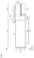
- FIG. 2 is a plan view of an antenna module including the antenna element according to the first embodiment when viewed from the X-axis direction.
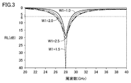
- FIG. 3 is a diagram showing a simulation result of reflection characteristics of a radiation electrode when an interval W1 shown in FIG. 2 is changed.
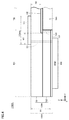
- FIG. 5 is a plan view of an antenna module including an antenna element according to a first modification of the first embodiment as viewed in the X-axis direction.
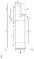
- FIG. 9 is a plan view of an antenna module including an antenna element according to a second modification of the first embodiment as viewed in the X-axis direction.
- FIG. 6 is a diagram showing a simulation result of the reflection characteristics of the radiation electrode when the interval W1 shown in FIG. 5 is changed.
- FIG. 6 is a diagram illustrating a simulation result of an isolation characteristic of two radiation electrodes when an interval W1 illustrated in FIG. 5 is changed.
- FIG. 14 is an external perspective view of an antenna module including the antenna element according to the second embodiment.
- FIG. 9 is a plan view of the antenna module of FIG. 8 viewed from the X-axis direction.
- FIG. 14 is a plan view of an antenna module according to a first modification of the second embodiment in an X-axis direction.
- FIG. 13 is a plan view of an antenna module according to a second modification of the second embodiment as viewed in the X-axis direction.
- FIG. 13 is a plan view of a communication device according to Embodiment 3 when viewed from the X-axis direction.
- FIG. 14 is a plan view of a communication device according to a first modification of the third embodiment as viewed in the X-axis direction.
- FIG. 21 is a plan view of a communication device according to a second modification of the third embodiment as viewed in the X-axis direction.
- FIG. 1 is a block diagram of a communication device 3000 including the antenna element 10.
- Examples of the communication device 3000 include a mobile terminal such as a mobile phone, a smartphone, and a tablet, and a personal computer having a communication function.
- the communication device 3000 includes an antenna module 1100 and a BBIC (Baseband Integrated Circuit) 2000 that forms a baseband signal processing circuit.
- the antenna module 1100 includes an RFIC (Radio Frequency Integrated Circuit) 140, which is an example of a high-frequency element, and the antenna element 10.
- RFIC Radio Frequency Integrated Circuit
- the communication device 3000 up-converts the baseband signal transmitted from the BBIC 2000 to the antenna module 1100 to a high-frequency signal and radiates it from the antenna element 10.
- Communication device 3000 down-converts the high-frequency signal received by antenna element 10 to a baseband signal and performs signal processing by BBIC 2000.
- the antenna element 10 is an antenna array in which a plurality of flat antenna elements (radiation conductors) are regularly arranged.
- FIG. 1 shows a configuration of RFIC 140 corresponding to four radiation electrodes 110 surrounded by a dotted line among a plurality of radiation electrodes 110 included in antenna element 10.
- the RFIC 140 includes switches 31A to 31D, 33A to 33D, and 37, power amplifiers 32AT to 32DT, low-noise amplifiers 32AR to 32DR, attenuators 34A to 34D, phase shifters 35A to 35D, and a signal combiner / demultiplexer. 36, a mixer 38, and an amplifier circuit 39.
- RFIC 140 is formed as a one-chip integrated circuit component including circuit elements (switch, power amplifier, low noise amplifier, attenuator, and phase shifter) corresponding to a plurality of radiation electrodes 110 included in antenna element 10, for example.
- the circuit element may be formed as a one-chip integrated circuit component for each radiation electrode 110 separately from the RFIC 140.
- the switches 31A to 31D and 33A to 33D are switched to the low noise amplifiers 32AR to 32DR, and the switch 37 is connected to the receiving amplifier of the amplifier circuit 39.
- the high-frequency signal received by the radiation electrode 110 passes through each signal path from the switches 31A to 31D to the phase shifters 35A to 35D, is multiplexed by the signal combiner / demultiplexer 36, and is converted into a baseband signal by the mixer 38.
- the signal is down-converted, amplified by the amplifier circuit 39, and transmitted to the BBIC 2000.
- the switches 31A to 31D and 33A to 33D are switched to the power amplifiers 32AT to 32DT, and the switch 37 is connected to the transmitting amplifier of the amplifier circuit 39.
- the baseband signal transmitted from the BBIC 2000 is amplified by the amplifier circuit 39 and up-converted by the mixer 38.
- the up-converted high-frequency signal is divided into four by the signal combining / demultiplexer 36, and is supplied to the radiation electrode 110 through each signal path from the phase shifters 35A to 35D to the switches 31A to 31D.
- the directivity of the antenna element 10 can be adjusted by individually adjusting the phase shift degrees of the phase shifters 35A to 35D arranged in each signal path.
- FIG. 2 is a plan view of the antenna module 1100 including the antenna element 100 according to the first embodiment as viewed from the X-axis direction.
- the X axis, the Y axis, and the Z axis are orthogonal to each other. The same applies to FIGS. 4, 5 and 8 to 14.
- the antenna module 1100 includes the antenna element 100 and the RFIC 140.
- the antenna element 100 includes a radiation electrode 111, a ground electrode 131 (first ground electrode), a ground electrode 132 (second ground electrode), via conductors 150 and 151, and a dielectric substrate 120.
- the normal direction of the radiation electrode 111 is the Z-axis direction.
- the dielectric substrate 120 has a flat plate-shaped portion 101 (first portion) and a portion 102 (second portion). In the Z-axis direction, the portion 102 is thinner than the portion 101.
- the dielectric substrate 120 is formed from an integral dielectric. That is, the dielectric substrate 120 is a substrate integrally formed of a dielectric material having a certain dielectric constant.
- the ground electrodes 131 and 132 are arranged in the portions 101 and 102, respectively.
- the ground electrodes 131 and 132 are connected by a via conductor 150.
- the dielectric substrate 120 is formed from an integral dielectric.
- the radiation electrode 111 faces the ground electrode 131 in the thickness direction (Z-axis direction) of the portion 101 in the portion 101, and faces the ground electrode 132 in the thickness direction (Z-axis direction) of the portion 102 in the portion 102.
- the width of the radiation electrode 111 in the Y-axis direction is 2.5 mm.
- the radiation electrode 111 does not entirely oppose the ground electrode 132, but a part of the radiation electrode 111 opposes the ground electrode 131 without opposing the ground electrode 132.
- the interval in which the radiation electrode 111 faces the ground electrode 132 without facing the ground electrode 132 in the Y-axis direction is W1.
- the via conductor 151 passes through the ground electrode 131 and connects the radiation electrode 111 and the RFIC 140.
- the via conductor 151 is insulated from the ground electrode 131.
- the RFIC 140 supplies a high-frequency signal to the radiation electrode 111 via the via conductor 151.
- RFIC 140 receives a high-frequency signal from radiation electrode 111 via via conductor 151.
- a space Spc is formed on the side of the portion 102 where the ground electrode 132 is arranged. Since other circuit elements are arranged in the space Spc, the distance between the radiation electrode 111 and the ground electrode 132 cannot be longer than H2.
- the radiation electrode 111 is arranged so as to face not only the ground electrode 132 but also the ground electrode 131.
- the distance H1 between the radiation electrode 111 and the ground electrode 131 is longer than the distance H2. Therefore, by making a part of the radiation electrode 111 face the ground electrode 131, the radiation characteristics of the antenna element 100 can be improved as compared with the case where the whole of the radiation electrode 111 faces the ground electrode 132.
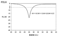
- FIG. 3 is a diagram showing a simulation result of the reflection characteristics (relation between frequency and return loss (RL: Return : Loss)) of the radiation electrode 111 when the interval W1 shown in FIG. 2 is changed.
- FIG. 3 shows the reflection characteristics in each case where the interval W1 is 1.0 mm, 1.5 mm, 2.0 mm, and 2.5 mm.
- the width of the bandwidth in which the reflection loss equal to or larger than the threshold is realized is one of the evaluation indexes of the radiation characteristics of the antenna element 100. That is, the wider the bandwidth, the better the radiation characteristics of the antenna element 100. Therefore, in FIG. 3, the radiation characteristics of the antenna element 100 when the interval W1 is changed are compared, paying attention to the width of the bandwidth where the reflection loss is 6 dB or more.
- the dielectric substrate is formed from an integral dielectric.
- the dielectric substrate may be formed from a plurality of dielectric layers.
- FIG. 4 is a plan view of the antenna module 1100A including the antenna element 100A according to the first modification of the first embodiment as viewed in the X-axis direction.
- the configuration of the antenna module 1100A is a configuration in which the antenna element 100 in FIG. 2 is replaced with 100A.
- the configuration of the antenna element 100A in FIG. 4 is a configuration in which the dielectric substrate 120 in FIG. 2 is replaced with 120A. The configuration other than these is the same, and thus the description will not be repeated.
- the dielectric substrate 120A includes a dielectric layer 121 (first dielectric layer) and a dielectric layer 122 (second dielectric layer).
- the dielectric layer 121 is a first substrate formed of a dielectric material having a first dielectric constant.
- the dielectric layer 122 is a second substrate formed of a dielectric material having a second dielectric constant.
- the dielectric substrate 120 is a substrate in which the dielectric layers 121 and 122 are integrated by heat welding or bonding with a connection member (for example, a solder bump).
- the first permittivity and the second permittivity may be different.
- the dielectric layer 121 is formed over the portions 101 and 102.
- the dielectric layer 122 is formed in the portion 101.
- the ground electrode 131 is disposed on the dielectric layer 122 in the portion 101.
- the ground electrode 132 is disposed on the dielectric layer 121 in the portion 102.
- the dielectric layers 121 and 122 may be welded to each other by heat, or may be bonded by a connecting member such as a solder bump.
- the dielectric constant of the dielectric layer 121 may be different from the dielectric constant of the dielectric layer 122.
- the antenna element including one radiation electrode has been described.
- the number of radiation electrodes may be two or more.
- an antenna element including two radiation electrodes will be described.
- FIG. 5 is a plan view of the antenna module 1100B including the antenna element 100B according to the second modification of the first embodiment as viewed in the X-axis direction.
- the configuration of the antenna module 1100B is a configuration in which the antenna element 100 in FIG. 2 is replaced with 100B.
- the configuration of antenna element 100B in FIG. 5 is a configuration in which radiation electrode 112 and via conductor 152 are added to the configuration of antenna element 100 in FIG. The configuration other than these is the same, and thus the description will not be repeated.
- the radiation electrode 112 is arranged on the portion 101 at a distance from the radiation electrode 111.
- the via conductor 152 penetrates the ground electrode 131, and connects the radiation electrode 112 and the RFIC 140.
- the via conductor 152 is insulated from the ground electrode 131.
- the RFIC 140 supplies a high-frequency signal to the radiation electrode 112 via the via conductor 152.
- RFIC 140 receives a high-frequency signal from radiation electrode 112 via via conductor 152.
- FIG. 6 is a diagram showing a simulation result of the reflection characteristics of the radiation electrode 112 when the interval W1 shown in FIG. 5 is changed.
- FIG. 6 shows the reflection characteristics in each case where the interval W1 is 1.0 mm, 1.50 mm, 2.0 mm, and 2.5 mm. Since the reflection characteristics in each case show almost the same mode of change, each reflection characteristic is drawn as the same curve in FIG. That is, the reflection characteristics of the radiation electrode 112 are hardly affected by the interval W1.
- FIG. 7 is a diagram showing a simulation result of the isolation characteristics (the relationship between isolation and frequency) of the two radiation electrodes 111 and 112 when the distance W1 is changed.
- FIG. 7 shows the isolation characteristics in each case where the interval W1 is 1.0 mm, 1.5 mm, 2.0 mm, and 2.5 mm.
- ⁇ ⁇ ⁇ Isolation of two radiation electrodes is an index indicating how much the two radiation electrodes are separated. In other words, the greater the isolation between the two radiation electrodes, the greater the proportion of signals that are not output from the other radiation electrode out of signals input from one radiation electrode.
- the minimum value of each isolation characteristic is within a range of about 1 dB. That is, the isolation characteristics of the radiation electrodes 111 and 112 are hardly affected by the interval W1.
- the radiation characteristics can be improved.
- FIG. 8 is an external perspective view of an antenna module 1200 including the antenna element 200 according to the second embodiment.
- FIG. 9 is a plan view of the antenna module 1200 of FIG. 8 viewed from the X-axis direction. Note that FIG. 8 does not show the ground electrodes 281 to 284 shown in FIG. 9 and a plurality of via conductors connected to the ground electrodes 281 to 284 shown in FIG.
- the antenna module 1200 includes the antenna element 200 and the RFIC 240.
- the antenna element 200 includes radiation electrodes 201 to 212, a dielectric substrate 220, a ground electrode 231 (first ground electrode), a ground electrode 232 (second ground electrode), via conductors 251 to 266, and a line conductor pattern. 271 to 274 and ground electrodes 281 to 284.
- the dielectric substrate 220 has a flat portion 291 (first portion), a portion 292 (second portion), and a flat portion 293. Portion 292 is thinner than portions 291 and 293. The dielectric substrate 220 is bent at the portion 292.
- the dielectric substrate 220 includes a dielectric layer 221 (first dielectric layer), a dielectric layer 222 (second dielectric layer), and a dielectric layer 223.
- the dielectric layer 221 is formed over the portions 291 to 293.
- the dielectric layer 221 is formed from a flexible material (flexible material).
- the dielectric layer 221 is bent at the portion 292.
- the dielectric layer 222 is formed in the portion 291.
- the dielectric layer 223 is formed in the portion 293.
- the dielectric substrate 220 may be formed from an integral dielectric.
- the radiation electrodes 201, 204, 207, and 210 are arranged along the X axis in the portion 291.
- the normal direction of the radiation electrodes 201, 204, 207, 210 is the Z-axis direction.
- the ground electrode 231 is disposed on the dielectric layer 222 so as to face each of the radiation electrodes 201, 204, 207, and 210 in the Z-axis direction.
- the via conductors 251, 255, 259, 263 penetrate the ground electrode 231, and connect the radiation electrodes 201, 204, 207, 210 and the RFIC 240, respectively.
- the via conductors 251, 255, 259, 263 are insulated from the ground electrode 231.
- the RFIC 240 supplies high-frequency signals to the radiation electrodes 201, 204, 207, and 210 via the via conductors 251, 255, 259, and 263, respectively.
- the RFIC 240 receives high-frequency signals from the radiation electrodes 201, 204, 207, 210 via the via conductors 251, 255, 259, 263, respectively.
- the radiation electrodes 203, 206, 209, and 212 are arranged in the portion 293 so as to be along the X axis.
- the normal direction of the radiation electrodes 203, 206, 209, 212 is the Y-axis direction.
- the ground electrode 232 is formed on the dielectric layer 221 over the portions 291 to 293.
- the ground electrode 232 faces the radiation electrodes 203, 206, 209, and 212 in the Y-axis direction.
- the ground electrode 232 is connected to the ground electrode 231.
- the ground electrodes 281 to 284 are formed over the portions 291 to 293, and are arranged on the dielectric layer 221 along the X axis.
- the ground electrodes 281 to 284 are connected to the ground electrode 232 by a plurality of via conductors.
- the radiation electrodes 202, 205, 208, 211 are formed over the portions 291 to 292 and are arranged along the X axis.
- the radiation electrodes 202, 205, 208, 211 face the ground electrode 231 in the Z-axis direction at the portion 291.
- the radiation electrodes 202, 205, 208, 211 face the ground electrode 232 in the thickness direction of the portion 292 at the portion 292.
- the distance in the Z-axis direction between the radiation electrodes 202, 205, 208, 211 and the ground electrode 231 is greater than the distance in the thickness direction of the portion 292 between the radiation electrodes 202, 205, 208, 211 and the ground electrode 232.
- a part of each of the radiation electrodes 202, 205, 208, and 211 does not face the ground electrode 232 at the portion 291 and faces the ground electrode 231.
- the via conductors 252, 256, 260, and 264 penetrate the ground electrode 231 and connect the radiation electrodes 202, 205, 208, 211 to the RFIC 240, respectively.
- the via conductors 252, 256, 260, 264 are insulated from the ground electrode 231.
- the line conductor patterns 271 to 274 are formed on the dielectric layer 221 over the portions 291 to 293.
- the line conductor pattern 271 is formed between the ground electrodes 232 and 281.
- the line conductor pattern 272 is formed between the ground electrodes 232 and 282.
- the line conductor pattern 273 is formed between the ground electrodes 232 and 283.
- the line conductor pattern 274 is formed between the ground electrodes 232 and 284.
- the via conductors 253, 257, 261, 265 penetrate the ground electrode 231 and connect the line conductor patterns 271 to 274 and the RFIC 240, respectively.
- the via conductors 253, 257, 261, 265 are insulated from the ground electrode 231.
- the via conductor 254 connects the line conductor pattern 271 and the radiation electrode 203.
- the via conductor 258 connects the line conductor pattern 272 and the radiation electrode 206.
- the via conductor 262 connects the line conductor pattern 273 and the radiation electrode 209.
- the via conductor 266 connects the line conductor pattern 274 and the radiation electrode 212.
- the RFIC 240 supplies high-frequency signals to the radiation electrodes 203, 206, 209, and 212 via the line conductor patterns 271 to 274, respectively.
- the RFIC 240 receives high-frequency signals from the radiation electrodes 203, 206, 209, and 212 via the line conductor patterns 271 to 274, respectively.
- the line direction (the thickness direction of the portion 292) and the normal direction (the Y-axis direction) of the radiation electrodes 203, 206, 209, and 212 are different from each other.
- transmission and reception of high-frequency signals having polarized waves having different excitation directions are easier than in the case where the normals of the plurality of radiation electrodes are parallel.
- the dielectric layer 221 is formed of a flexible material, the stress generated in the bent portion 292 can be reduced. Therefore, in portions 291 and 293, the planarity of the surface of dielectric substrate 220 can be maintained. Therefore, it is possible to suppress the normal direction of the radiation electrodes 201 to 212 from being shifted from a desired direction. As a result, it is possible to suppress a decrease in the characteristics of the antenna element 200 due to the bending of the dielectric substrate 220.
- FIG. 10 is a plan view of the antenna module 1200A according to the first modification of the second embodiment viewed from the X-axis direction.
- the via conductors 253, 257, 261, 265 and the line conductor patterns 271 to 274 are removed from the configuration of the antenna module 1200 in FIG.
- via conductors 251, 255, 259, 263 of antenna module 1200 in FIG. 9 are replaced with via conductors 251A, 255A, 259A, 263A, respectively.
- via conductors 252, 256, 260, 264 of antenna module 1200 in FIG. 9 are replaced with via conductors 252A, 256A, 260A, 264A, respectively.
- antenna module 1200A via conductors 254, 258, 262, 266 of antenna module 1200 in FIG. 9 are replaced with via conductors 254A, 258A, 262A, 266A, respectively.
- RFIC 240 is replaced with 240A.
- Line conductor patterns 271A to 274A and 275 to 278, via conductors 251B, 255B, 259B and 263B, and via conductors 252B, 256B, 260B and 264B are added to the antenna module 1200A. The configuration other than these is the same, and thus the description will not be repeated.
- RFIC 240A is arranged on dielectric layer 223 so as to face ground electrode 232 at portion 293.
- the line conductor patterns 271A to 274A are formed on the dielectric layer 221 over the portions 291 to 293.
- the line conductor pattern 271A is formed between the ground electrodes 232 and 281.
- the line conductor pattern 272A is formed between the ground electrodes 232 and 282.
- the line conductor pattern 273A is formed between the ground electrodes 232 and 283.
- the line conductor pattern 274A is formed between the ground electrodes 232 and 284.
- the via conductor 251A connects the line conductor pattern 271A and the radiation electrode 201.
- the via conductor 255A connects the line conductor pattern 272A and the radiation electrode 204.
- the via conductor 259A connects the line conductor pattern 273A and the radiation electrode 207.
- the via conductor 263A connects the line conductor pattern 274A and the radiation electrode 210.
- the via conductors 251B, 255B, 259B, 263B penetrate the ground electrode 232 and connect the line conductor patterns 271A to 274A and the RFIC 240A, respectively.
- the via conductors 251B, 255B, 259B, 263B are insulated from the ground electrode 232.
- the RFIC 240A supplies high-frequency signals to the radiation electrodes 201, 204, 207, and 210 via the line conductor patterns 271A to 274A, respectively.
- the RFIC 240A receives high-frequency signals from the radiation electrodes 201, 204, 207, and 210 via the line conductor patterns 271A to 274A, respectively.
- the line conductor patterns 275 to 278 are formed on the dielectric layer 221 over the portions 291 to 293.
- the line conductor pattern 275 is formed between the ground electrodes 232 and 281.
- the line conductor pattern 276 is formed between the ground electrodes 232 and 282.
- the line conductor pattern 277 is formed between the ground electrodes 232 and 283.
- the line conductor pattern 278 is formed between the ground electrodes 232 and 284.
- the via conductor 252A connects the line conductor pattern 275 and the radiation electrode 202.
- the via conductor 256A connects the line conductor pattern 276 and the radiation electrode 205.
- the via conductor 260A connects the line conductor pattern 277 and the radiation electrode 208.
- the via conductor 264A connects the line conductor pattern 278 and the radiation electrode 211.
- the via conductors 252B, 256B, 260B, 264B penetrate the ground electrode 232 and connect the line conductor patterns 275 to 278 to the RFIC 240A, respectively.
- the via conductors 252B, 256B, 260B, 264B are insulated from the ground electrode 232.
- the RFIC 240A supplies a high-frequency signal to the radiation electrodes 202, 205, 208, 211 via the line conductor patterns 275 to 278, respectively.
- the RFIC 240A receives high-frequency signals from the radiation electrodes 202, 205, 208, 211 via the line conductor patterns 275 to 278, respectively.
- the via conductors 254A, 258A, 262A, 266A penetrate the ground electrode 232, and connect the radiation electrodes 203, 206, 209, 212 to the RFIC 240A, respectively.
- the via conductors 254A, 258A, 262A, 266A are insulated from the ground electrode 232.
- the RFIC 240A supplies a high-frequency signal to the radiation electrodes 203, 206, 209, and 212 via the via conductors 254A, 258A, 262A, and 266A, respectively.
- RFIC 240A receives high-frequency signals from radiation electrodes 203, 206, 209, and 212 via via conductors 254A, 258A, 262A, and 266A, respectively.
- FIG. 11 is a plan view of an antenna module 1200B according to a second modification of the second embodiment as viewed in the X-axis direction.
- the configuration of the antenna module 1200B is a configuration in which the antenna element 200 of the antenna module 1200 in FIG. 9 is replaced with 200B.
- the configuration of the antenna element 200B is such that the dielectric substrate 220 is replaced with 220B, the radiation electrodes 202B, 205B, 208B, 211B, the radiation electrodes 203B, 206B, 209B, 212B, the ground electrodes 232B, 281B to 284B, the via conductors.
- the configuration of the dielectric substrate 220B is such that the dielectric layer 221 of the dielectric substrate 220 is replaced with 221B, and portions 292B, 293B and a dielectric layer 223B are added to the dielectric substrate 220. Other than these, the description is the same, and the description will not be repeated.
- the portion 293B is flat. Portion 292B is thinner than portions 291 and 293B. In the dielectric substrate 220B, the portion 292B connects the portion 291 extending in the Y-axis direction and the portion 293B extending in the Z-axis direction.
- the dielectric layer 221B is formed of a flexible material (flexible material).
- the dielectric substrate 220B is bent at the portion 292B (second portion) in addition to the portion 292.
- the dielectric layer 223B is formed in the portion 293B. Note that the dielectric substrate 220B may be formed from an integral dielectric.
- the radiation electrodes 203B, 206B, 209B, and 212B are arranged along the X axis in the portion 293B.
- the normal direction of the radiation electrodes 203B, 206B, 209B, and 212B is the Y-axis direction.
- the ground electrode 232B is formed on the dielectric layer 221B over the portions 291, 292B, and 293B.
- the ground electrode 232B faces the radiation electrodes 203B, 206B, 209B, and 212B in the Y-axis direction.
- the ground electrode 232B is connected to the ground electrode 231B.
- the ground electrodes 281B to 284B are formed over the portions 291, 292B, and 293B, and are arranged on the dielectric layer 221B along the X axis.
- the ground electrodes 281B to 284B are connected to the ground electrode 232B by a plurality of via conductors.
- the radiation electrodes 202B, 205B, 208B, 211B are formed over the portions 291 to 292B and are arranged along the X axis.
- the radiation electrodes 202B, 205B, 208B, and 211B face the ground electrode 231 in the Z-axis direction at the portion 291.
- the radiation electrodes 202B, 205B, 208B and 211B face the ground electrode 232B in the thickness direction of the portion 292B in the portion 292B.
- the distance in the Z-axis direction between the radiation electrodes 202B, 205B, 208B, 211B and the ground electrode 231 is larger than the distance in the thickness direction of a portion 292B between the radiation electrodes 202B, 205B, 208B, 211B and the ground electrode 232B.
- a part of each of the radiation electrodes 202B, 205B, 208B, and 211B does not face the ground electrode 232B at the portion 291 and faces the ground electrode 231.
- the via conductors 252B, 256B, 260B, 264B penetrate the ground electrode 231 to connect the radiation electrodes 202B, 205B, 208B, 211B and the RFIC 240, respectively.
- the via conductors 252B, 256B, 260B, 264B are insulated from the ground electrode 231.
- the line conductor patterns 271B to 274B are formed on the dielectric layer 221B over the portions 291, 292B and 293B.
- the line conductor pattern 271B is formed between the ground electrodes 232B and 281B.
- the line conductor pattern 272B is formed between the ground electrodes 232B and 282B.
- the line conductor pattern 273B is formed between the ground electrodes 232B and 283B.
- the line conductor pattern 274B is formed between the ground electrodes 232B and 284B.
- the via conductors 253B, 257B, 261B, and 265B penetrate the ground electrode 231 and connect the line conductor patterns 271B to 274B and the RFIC 240, respectively.
- the via conductors 253B, 257B, 261B, 265B are insulated from the ground electrode 231.
- the via conductor 254B connects the line conductor pattern 271B and the radiation electrode 203B.
- the via conductor 258B connects the line conductor pattern 272B and the radiation electrode 206B.
- the via conductor 262B connects the line conductor pattern 273B and the radiation electrode 209B.
- the via conductor 266B connects the line conductor pattern 274B and the radiation electrode 212B.
- the RFIC 240 supplies high-frequency signals to the radiation electrodes 203B, 206B, 209B, and 212B via the line conductor patterns 271B to 274B, respectively.
- the RFIC 240 receives high-frequency signals from the radiation electrodes 203B, 206B, 209B, and 212B via the line conductor patterns 271B to 274B, respectively.
- the normal direction (Z-axis direction) of the radiation electrodes 201, 204, 207, 210 and the radiation electrodes 202, 205, 208, 211 (The thickness direction of the portion 292)
- the normal direction (Y-axis direction) of the radiation electrodes 203, 206, 209, 212, 203B, 206B, 209B, and 212B and the radiation electrodes 202B, 205B, 208B, and 211B.
- the normal directions (the thickness direction of the portion 292B) are different from each other.
- transmission and reception of high-frequency signals having polarizations having different excitation directions are easier than in the case where the normals of the plurality of radiation electrodes are parallel.
- the dielectric layer 221B is formed from a flexible material, the stress generated in the bent portions 292 and 292B can be reduced. Therefore, in the portions 291, 293, and 293B, the planarity of the surface of the dielectric substrate 220B can be maintained. Therefore, it is possible to suppress the normal direction of the radiation electrodes 201 to 212, the radiation electrodes 202B, 205B, 208B, 211B, and the radiation electrodes 203B, 206B, 209B, 212B from deviating from a desired direction. As a result, it is possible to suppress a decrease in the characteristics of the antenna element 200B due to the bending of the dielectric substrate 220B.
- the radiation characteristics can be improved.
- FIG. 12 is a plan view of the communication device 3000 according to Embodiment 3 when viewed from the X-axis direction.
- the communication device 3000 includes a BBIC 2000, an antenna module 1300, and a mounting board 320.
- the configuration of the antenna module 1300 is such that a connector 321 is added to the antenna module 1200 shown in FIG. Other than that, the description is the same, and thus the description will not be repeated.
- the connector 321 is disposed on the dielectric layer 222 of the portion 291.
- the connector 321 is connected to the RFIC 240 by a power supply wiring formed inside the dielectric layer 222.
- the connector 322 is arranged on the mounting board 320. The connector 322 is detachably connected to the connector 321.
- the BBIC 2000 is disposed on the surface of the mounting substrate 320 by a connection member such as a solder bump.
- the BBIC 2000 is connected to the connector 322 by a power supply wiring formed inside the mounting board 320.
- the BBIC 2000 transmits a baseband signal to the RFIC 240 and receives a baseband signal from the RFIC 240 via the power supply wiring and the connector 322.
- the BBIC 2000 and the RFIC 240 can be connected from a greater distance by running FPCs (Flexible Printed Circuits).
- FIG. 13 is a plan view of a communication device 3000A according to a first modification of the third embodiment as viewed from the X-axis direction.
- the communication device 3000A includes a BBIC 2000, an antenna module 1300A, and a mounting substrate 320A.
- the configuration of the antenna module 1300A is a configuration in which the antenna element 200 of the antenna module 1200 in FIG. 9 is replaced with 200A.
- the radiation electrodes 203, 206, 209, 212, the via conductors 254, 258, 262, 266, and the dielectric layer 223 are removed from the antenna element 200 of FIG. This is an added configuration. Other than these, the description is the same, and therefore, the description will not be repeated.
- the connector 331 is disposed on the dielectric layer 221 of the portion 293.
- the connector 331 is connected to the line conductor patterns 271 to 274.
- the BBIC 2000 is arranged on the surface of the mounting substrate 320A by a connection member such as a solder bump.
- the connector 332 is arranged on the mounting board 320A. The connector 332 is detachably connected to the connector 331.
- the BBIC 2000 is connected to the connector 332 by a power supply wiring formed inside the mounting board 320A.
- the BBIC 2000 transmits a baseband signal to the RFIC 240 and receives a baseband signal from the RFIC 240 via the power supply wiring, the connectors 332, 331, the line conductor patterns 271 to 274, and the via conductors 253, 257, 261, 265. .
- FIG. 14 is a plan view of a communication device 3000B according to a second modification of the third embodiment as viewed from the X-axis direction.
- Communication device 3000B has a configuration in which antenna module 1300 of communication device 3000 in FIG. 12 is replaced with 1300B.
- the configuration of the antenna module 1300B is such that the antenna element 200 and the RFIC 240 of the antenna module 1300 are replaced with an antenna element 200C and an RFIC 240B, respectively.
- the radiation electrodes 203, 206, 209, and 212 of the antenna element 200, the dielectric substrate 220, the line conductor patterns 271 to 274, the ground electrode 232, the via conductors 253, 257, 261, 265, and the via conductor 254 , 258, 262, 266 are radiation electrodes 203C, 206C, 209C, 212C, dielectric substrate 220C, line conductor patterns 271C to 274C, ground electrode 232C, via conductors 253C, 257C, 261C, 265C, and via conductors 254C, 258C. , 262C and 266C, respectively.
- the antenna element 200C includes radiation electrodes 203D, 206D, 209D, 212D, via conductors 253D, 257D, 261D, 265D, via conductors 254D, 258D, 262D, 266D, line conductor patterns 271D to 274D, and a ground electrode 281C. 284C have been added.
- Dielectric substrate 220C has a configuration in which dielectric layers 221 and 223 and portion 293 are replaced with dielectric layers 221C, 223C and portion 293C, respectively, and a dielectric layer 224 and portions 294 and 295 are added. is there. Other than these, the description is the same, and the description will not be repeated.
- the dielectric layer 221C (first dielectric layer) is formed from a flexible material.
- the dielectric layer 221C is bent at the portions 292 and 294.
- the flat portion 295 is connected to the portion 294 and extends in the Y-axis direction.
- the dielectric layer 224 is formed in the portion 295.
- the dielectric layer 223C is formed in the portion 293.
- the dielectric substrate 220C is formed so as to wind the end of the mounting substrate 320. Note that the dielectric substrate 220C may be formed from an integral dielectric.
- the portion 295 may be fixed to a housing (not shown) via an adhesive layer.
- the portion 295 may be formed to be close to the mounting substrate 320.
- the radiation electrodes 203C, 206C, 209C, and 212C are formed from the portions 293C to 294, and are arranged along the X axis.
- the radiation electrodes 203C, 206C, 209C, and 212C face the ground electrode 232C in the Y-axis direction at the portion 293C.
- the radiation electrodes 203C, 206C, 209C, and 212C face the ground electrode 232C in the thickness direction of the portion 294 at the portion 294.
- the radiation electrodes 203D, 206D, 209D, and 212D are arranged along the X axis in the portion 295.
- the normal direction of the radiation electrodes 203D, 206D, 209D, and 212D is the Z-axis direction.
- the ground electrode 232C is formed on the dielectric layer 221C over the portions 291, 292, 293C, 294, and 295.
- the ground electrode 232C faces the radiation electrodes 203D, 206D, 209D, and 212D in the Z-axis direction.
- the ground electrode 232C is connected to the ground electrode 231.
- the ground electrodes 281C to 284C are formed over the portions 293C, 294, and 295, and are arranged on the dielectric layer 221C along the X axis.
- the ground electrodes 281C to 284C are connected to the ground electrode 232C by a plurality of via conductors.
- the line conductor patterns 271C to 274C are formed on the dielectric layer 221C over the portions 291, 292, and 293C.
- the line conductor pattern 271C is formed between the ground electrodes 232C and 281.
- the line conductor pattern 272C is formed between the ground electrodes 232C and 282.
- the line conductor pattern 273C is formed between the ground electrodes 232C and 283.
- the line conductor pattern 274C is formed between the ground electrodes 232C and 284.
- the via conductors 253C, 257C, 261C, 265C penetrate the ground electrode 231 to connect the line conductor patterns 271C to 274C and the RFIC 240B, respectively.
- the via conductors 253C, 257C, 261C, 265C are insulated from the ground electrode 231.
- the via conductor 254C connects the line conductor pattern 271C and the radiation electrode 203C.
- the via conductor 258C connects the line conductor pattern 272C and the radiation electrode 206C.
- the via conductor 262C connects the line conductor pattern 273C and the radiation electrode 209C.
- the via conductor 266C connects the line conductor pattern 274C and the radiation electrode 212C.
- the RFIC 240B supplies high-frequency signals to the radiation electrodes 203C, 206C, 209C, and 212C via the line conductor patterns 271C to 274C, respectively.
- the RFIC 240B receives high-frequency signals from the radiation electrodes 203C, 206C, 209C, and 212C via the line conductor patterns 271C to 274C, respectively.
- the line conductor patterns 271D to 274D are formed on the dielectric layer 221C over the portions 291, 292, 293C, 294, and 295.
- the line conductor pattern 271D is formed between the ground electrodes 232C and 281C, and is formed between the ground electrodes 232C and 281C.
- the line conductor pattern 272D is formed between the ground electrodes 232C and 282C and between the ground electrodes 232C and 282C.
- the line conductor pattern 273D is formed between the ground electrodes 232C and 283, and is formed between the ground electrodes 232C and 283C.
- the line conductor pattern 274D is formed between the ground electrodes 232C and 284C and between the ground electrodes 232C and 284C.
- the via conductors 253D, 257D, 261D, and 265D penetrate the ground electrode 231 to connect the line conductor patterns 271D to 274D and the RFIC 240B, respectively.
- the via conductors 253D, 257D, 261D, 265D are insulated from the ground electrode 231.
- the via conductor 254D connects the line conductor pattern 271D and the radiation electrode 203D.
- the via conductor 258D connects the line conductor pattern 272D and the radiation electrode 206D.
- the via conductor 262D connects the line conductor pattern 273D and the radiation electrode 209D.
- the via conductor 266D connects the line conductor pattern 274D and the radiation electrode 212D.
- the RFIC 240B supplies high-frequency signals to the radiation electrodes 203D, 206D, 209D, and 212D via the line conductor patterns 271D to 274D, respectively.
- the RFIC 240B receives high-frequency signals from the radiation electrodes 203D, 206D, 209D, and 212D via the line conductor patterns 271D to 274D, respectively.
- the radiation direction is normal to the radiation electrodes 201, 204, 207, 210, 203D, 206D, 209D, and 212D (Z-axis direction).
- the normal direction of the electrodes 202, 205, 208, and 211 (the thickness direction of the portion 292)
- the radiation electrodes 203C, 206C, and 209C , 212C are different from each other in the normal direction (the thickness direction of the portion 294).
- transmission and reception of high-frequency signals having polarizations having different excitation directions are easier than in the case where the normals of the plurality of radiation electrodes are parallel.
- the dielectric layer 221C is formed of a flexible material, the stress generated in the bent portions 292 and 294 can be reduced. In the portions 291, 293C, and 295, the planarity of the surface of the dielectric substrate 220C can be maintained. Therefore, it is possible to suppress the normal direction of each radiation electrode from being shifted from a desired direction. As a result, it is possible to suppress a decrease in the characteristics of the antenna element 200C due to the bending of the dielectric substrate 220C.
- the radiation characteristics of the antenna element can be improved.
Landscapes
- Engineering & Computer Science (AREA)
- Computer Networks & Wireless Communication (AREA)
- Microelectronics & Electronic Packaging (AREA)
- Details Of Aerials (AREA)
- Waveguide Aerials (AREA)
Abstract
アンテナ素子(100)は、誘電体基板(120)と、第1接地電極(131)と、第2接地電極(132)と、ビア導体(150)と、放射電極(111)とを備える。誘電体基板(120)は、平板状の第1部分(101)、および第1部分(101)より薄い第2部分(102)を有する。第1接地電極(131)は、第1部分(101)に配置されている。第2接地電極(132)は、第2部分(102)に配置されている。ビア導体(150)は、第1接地電極(131)と第2接地電極(132)とを接続する。放射電極(111)と第1接地電極(131)との第1厚み方向の距離(H1)は、放射電極(111)と第2接地電極(132)との第2厚み方向の距離(H2)より大きい。放射電極(111)の一部は、第2接地電極(132)と対向せず、かつ第1接地電極(131)と対向する。
Description
本発明は、放射電極および接地電極が対向するように配置されたアンテナ素子、当該アンテナ素子を備えるアンテナモジュール、および当該アンテナモジュールを備える通信装置に関する。
従来、放射電極および接地電極が対向するように配置されたアンテナ素子が知られている。たとえば、国際公開第2012/081288号(特許文献1)には、放射電極および接地導体板が対向するように配置されたアンテナを備える高周波用パッケージが開示されている。当該アンテナは、無給電素子を含むスタック型パッチアンテナとして形成され、多層基板においてキャビティと異なる位置に設けられている。当該高周波用パッケージによれば、厚さを抑制しつつ、受信可能な高周波信号の帯域を広げることができる。
アンテナ素子において、対向するように放射電極および接地電極が配置される場合、放射電極と接地電極との容量結合を適切な強さに保つため、接地電極から或る程度の距離だけ離間させる必要があることが知られている。たとえば、特許文献1に開示されている高周波パッケージにおいて、キャビティが形成されている多層基板の部分は、キャビティが形成されていない多層基板の部分よりも薄い。放射電極は、キャビティが形成されていない多層基板の部分に配置されることにより、接地導体板から或る程度の距離だけ離されている。
特許文献1に開示されている高周波パッケージのように、厚さの異なる部分を有する誘電体基板に放射電極と接地電極とを対向するように配置する場合、放射電極と接地電極とをより離間させるために、厚い部分に両者を配置するのが通常である。しかし、アンテナ素子が配置されるスペースによっては、誘電体基板において厚く成形可能な部分が制限される場合がある。そのような場合、誘電体基板の薄い部分に放射電極と接地電極とを対向するように配置せざるを得ず、放射電極と接地電極との距離を確保できない可能性がある。その結果、アンテナ素子の放射特性の改善が困難になり得る。
本発明は上記のような課題を解決するためになされたものであり、その目的は放射電極および接地電極が対向するように配置されたアンテナ素子において、放射特性を改善することである。
本発明の一実施の形態に係るアンテナ素子は、誘電体基板と、第1接地電極と、第2接地電極と、ビア導体と、放射電極とを備える。誘電体基板は、第1部分および第2部分を有する。第1部分は、平板状である。第2部分は、第1部分よりも薄い。第1接地電極は、第1部分に配置されている。第2接地電極は、第2部分に配置されている。ビア導体は、第1接地電極と第2接地電極とを接続する。放射電極は、第1部分において第1部分の第1厚み方向に第1接地電極と対向する。放射電極は、第2部分において第2部分の第2厚み方向に第2接地電極と対向する。放射電極と第1接地電極との第1厚み方向の距離は、放射電極と第2接地電極との第2厚み方向の距離より大きい。放射電極の一部は、第2接地電極と対向せず、かつ第1接地電極と対向する。
本発明の一実施の形態に係るアンテナ素子によれば、放射電極の一部が第2接地電極と対向せず、かつ第1接地電極と対向することにより、放射特性を改善することができる。
以下、実施の形態について図面を参照しながら詳細に説明する。なお、図中同一または相当部分には同一符号を付してその説明は原則として繰り返さない。
図1は、アンテナ素子10を備える通信装置3000のブロック図である。通信装置3000としては、携帯電話,スマートフォン,タブレットなどの携帯端末、あるいは通信機能を有するパーソナルコンピュータなどを挙げることができる。
図1に示されるように、通信装置3000は、アンテナモジュール1100と、ベースバンド信号処理回路を構成するBBIC(Baseband Integrated Circuit)2000とを備える。アンテナモジュール1100は、高周波素子の一例であるRFIC(Radio Frequency Integrated Circuit)140と、アンテナ素子10とを備える。
通信装置3000は、BBIC2000からアンテナモジュール1100へ伝達されたベースバンド信号を高周波信号にアップコンバートしてアンテナ素子10から放射する。通信装置3000は、アンテナ素子10で受信した高周波信号をベースバンド信号にダウンコンバートしてBBIC2000にて信号処理する。
アンテナ素子10は、複数の平板状のアンテナ素子(放射導体)が、規則的に配置されたアンテナアレイである。図1においては、アンテナ素子10に含まれる複数の放射電極110のうち、点線で囲まれた4つの放射電極110に対応するRFIC140の構成が示されている。
RFIC140は、スイッチ31A~31D,33A~33D,37と、パワーアンプ32AT~32DTと、ローノイズアンプ32AR~32DRと、減衰器34A~34Dと、移相器35A~35Dと、信号合成/分波器36と、ミキサ38と、増幅回路39とを備える。
RFIC140は、たとえば、アンテナ素子10に含まれる複数の放射電極110に対応する回路要素(スイッチ、パワーアンプ、ローノイズアンプ、減衰器、および移相器)を含む1チップの集積回路部品として形成される。あるいは、当該回路要素については、RFIC140とは別に、放射電極110毎に1チップの集積回路部品として形成されてもよい。
高周波信号を受信する場合、スイッチ31A~31D,33A~33Dがローノイズアンプ32AR~32DR側へ切換えられるとともに、スイッチ37が増幅回路39の受信側アンプに接続される。
放射電極110によって受信された高周波信号は、スイッチ31A~31Dから移相器35A~35Dまでの各信号経路を経由し、信号合成/分波器36によって合波され、ミキサ38によってベースバンド信号にダウンコンバートされ、増幅回路39によって増幅されてBBIC2000へ伝達される。
高周波信号をアンテナ素子10から送信する場合には、スイッチ31A~31D,33A~33Dがパワーアンプ32AT~32DT側へ切換えられるとともに、スイッチ37が増幅回路39の送信側アンプに接続される。
BBIC2000から伝達されたベースバンド信号は、増幅回路39によって増幅され、ミキサ38によってアップコンバートされる。アップコンバートされた高周波信号は、信号合成/分波器36によって4分波され、移相器35A~35Dからスイッチ31A~31Dまでの各信号経路を通過して放射電極110に給電される。各信号経路に配置された移相器35A~35Dの移相度が個別に調整されることにより、アンテナ素子10の指向性を調整することが可能となる。
[実施の形態1]
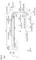
図2は、実施の形態1に係るアンテナ素子100を備えるアンテナモジュール1100をX軸方向から平面視した図である。図2において、X軸、Y軸、およびZ軸は互いに直交している。図4,図5,図8~図14においても同様である。
図2は、実施の形態1に係るアンテナ素子100を備えるアンテナモジュール1100をX軸方向から平面視した図である。図2において、X軸、Y軸、およびZ軸は互いに直交している。図4,図5,図8~図14においても同様である。
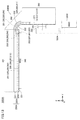
図2に示されるように、アンテナモジュール1100は、アンテナ素子100と、RFIC140とを備える。アンテナ素子100は、放射電極111と、接地電極131(第1接地電極)と、接地電極132(第2接地電極)と、ビア導体150,151と、誘電体基板120とを備える。放射電極111の法線方向は、Z軸方向である。
誘電体基板120は、平板状の部分101(第1部分)と、部分102(第2部分)とを有する。Z軸方向において、部分102は、部分101より薄い。誘電体基板120は、一体の誘電体から形成されている。すなわち、誘電体基板120は、或る誘電率を有する誘電体材料によって一体成型された基板である。
接地電極131,132は、部分101,102にそれぞれ配置されている。接地電極131と132とは、ビア導体150によって接続されている。誘電体基板120は、一体の誘電体から形成されている。
放射電極111は、部分101において部分101の厚み方向(Z軸方向)に接地電極131と対向するとともに、部分102において部分102の厚み方向(Z軸方向)に接地電極132と対向するように、部分101から102に亘って誘電体基板120に配置されている。Z軸方向における放射電極111と接地電極131,132との距離は、それぞれH1,H2(=H1/2)である。放射電極111のY軸方向の幅は、2.5mmである。放射電極111は、全体が接地電極132と対向するのではなく、放射電極111の一部が接地電極132とは対向せずに接地電極131と対向する。Y軸方向において放射電極111が接地電極132と対向せずに接地電極132と対向する間隔は、W1である。
ビア導体151は、接地電極131を貫通し、放射電極111とRFIC140とを接続している。ビア導体151は、接地電極131から絶縁されている。
RFIC140は、ビア導体151を介して放射電極111に高周波信号を供給する。RFIC140は、ビア導体151を介して放射電極111から高周波信号を受ける。
部分102において接地電極132が配置されている側には、スペースSpcが形成されている。スペースSpcには他の回路素子が配置されるため、放射電極111と接地電極132との距離をH2より長くすることができない。
そこで、実施の形態1においては、接地電極132に加えて接地電極131とも対向するように放射電極111を配置する。放射電極111と接地電極131との距離H1は、距離H2よりも長い。そのため、放射電極111の一部を接地電極131と対向させることにより、放射電極111の全部が接地電極132と対向している場合よりも、アンテナ素子100の放射特性を改善することができる。
図3は、図2に示される間隔W1を変化させた場合の、放射電極111の反射特性(周波数と反射損失(RL:Return Loss)との関係)のシミュレーション結果を示す図である。図3においては、間隔W1が、1.0mm,1.5mm,2.0mm,2.5mmである各場合の反射特性が示されている。
反射損失が大きい程、RFIC140から放射電極111に供給された高周波信号のうち、放射電極111から外部に放射された信号の割合が大きいことを意味する。そのため、しきい値以上の反射損失が実現される帯域幅の広さは、アンテナ素子100の放射特性の評価指標の1つになる。すなわち、当該帯域幅が広いほど、アンテナ素子100の放射特性は良好といえる。そこで、図3においては、反射損失が6dB以上となる帯域幅の広さに着目して、間隔W1を変化させた場合のアンテナ素子100の放射特性を比較する。
図3に示されるように、間隔W1が広いほど、接地電極131と対向する放射電極111の部分が大きいため、反射損失が6dB以上となる帯域幅は広い。すなわち、接地電極131と対向する放射電極111の部分が大きいほど、アンテナ素子100の放射特性は改善される。
[実施の形態1の変形例1]
実施の形態1においては、誘電体基板が一体の誘電体から形成されている場合について説明した。誘電体基板は、複数の誘電体層から形成されてもよい。
実施の形態1においては、誘電体基板が一体の誘電体から形成されている場合について説明した。誘電体基板は、複数の誘電体層から形成されてもよい。
図4は、実施の形態1の変形例1に係るアンテナ素子100Aを備えるアンテナモジュール1100AをX軸方向から平面視した図である。アンテナモジュール1100Aの構成は、図2のアンテナ素子100が100Aに置き換えられた構成である。図4のアンテナ素子100Aの構成は、図2の誘電体基板120が120Aに置き換えられた構成である。これら以外の構成は同様であるため、説明を繰り返さない。
図4に示されるように、誘電体基板120Aは、誘電体層121(第1誘電体層)と誘電体層122(第2誘電体層)とを含む。誘電体層121は、第1誘電率を有する誘電体材料によって成型された第1基板である。誘電体層122は、第2誘電率を有する誘電体材料によって成型された第2基板である。誘電体基板120は、誘電体層121と122とが熱による溶着あるいは接続部材(たとえばはんだバンプ)による接着等により一体化された基板である。第1誘電率と第2誘電率とは異なっていてもよい。
誘電体層121は、部分101および102に亘って形成されている。誘電体層122は、部分101に形成されている。接地電極131は、部分101において誘電体層122に配置されている。接地電極132は、部分102において誘電体層121に配置されている。誘電体層121と122とは、熱によって互いに溶着されてもよいし、はんだバンプなどの接続部材によって接着されてもよい。誘電体層121の誘電率は、誘電体層122の誘電体率と異なっていてもよい。
[実施の形態1の変形例2]
実施の形態1および変形例1においては、1つの放射電極を備えるアンテナ素子について説明した。放射電極の数は、2以上であってもよい。実施の形態1の変形例2においては、2つの放射電極を備えるアンテナ素子について説明する。
実施の形態1および変形例1においては、1つの放射電極を備えるアンテナ素子について説明した。放射電極の数は、2以上であってもよい。実施の形態1の変形例2においては、2つの放射電極を備えるアンテナ素子について説明する。
図5は、実施の形態1の変形例2に係るアンテナ素子100Bを備えるアンテナモジュール1100BをX軸方向から平面視した図である。アンテナモジュール1100Bの構成は、図2のアンテナ素子100が100Bに置き換えられた構成である。図5のアンテナ素子100Bの構成は、図2のアンテナ素子100の構成に放射電極112およびビア導体152が追加された構成である。これら以外の構成は同様であるため、説明を繰り返さない。
図5に示されるように、放射電極112は、放射電極111から離間して部分101に配置されている。ビア導体152は、接地電極131を貫通し、放射電極112とRFIC140とを接続している。ビア導体152は、接地電極131から絶縁されている。
RFIC140は、ビア導体152を介して放射電極112に高周波信号を供給する。RFIC140は、ビア導体152を介して放射電極112から高周波信号を受ける。
図6は、図5に示される間隔W1を変化させた場合の、放射電極112の反射特性のシミュレーション結果を示す図である。図6においては、間隔W1が、1.0mm,1.50mm,2.0mm,2.5mmである各場合の反射特性が示されている。各場合の反射特性は、ほとんど同じ変化の態様を示すため、各反射特性は、図6において同一の曲線として描かれている。すなわち、放射電極112の反射特性は、間隔W1にほとんど影響されない。
図7は、間隔W1を変化させた場合の、2つの放射電極111,112のアイソレーション特性(アイソレーションと周波数との関係)のシミュレーション結果を示す図である。図7においては、間隔W1が、1.0mm,1.5mm,2.0mm,2.5mmである各場合のアイソレーション特性が示されている。
2つの放射電極のアイソレーションとは、当該2つの放射電極がどれだけ分離されているかを示す指標である。すなわち、2つの放射電極のアイソレーションが大きいほど、一方の放射電極から入力された信号のうち、他方の放射電極から出力されない信号の割合が大きい。
図7に示される周波数帯において、各アイソレーション特性の極小値は、1dB程度の範囲内に収まっている。すなわち、放射電極111,112のアイソレーション特性は、間隔W1にほとんど影響されない。
以上、実施の形態1および変形例1,2に係るアンテナ素子によれば、放射特性を改善することができる。
[実施の形態2]
実施の形態2においては、アンテナ素子の誘電体基板が屈曲している場合について説明する。
実施の形態2においては、アンテナ素子の誘電体基板が屈曲している場合について説明する。
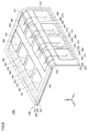
図8は、実施の形態2に係るアンテナ素子200を備えるアンテナモジュール1200の外観斜視図である。図9は、図8のアンテナモジュール1200をX軸方向から平面視した図である。なお、図8においては、各構成要素の接続関係を見易くするため、図9に示される接地電極281~284、および接地電極281~284に接続される複数のビア導体が示されていない。
図8および図9に示されるように、アンテナモジュール1200は、アンテナ素子200と、RFIC240とを備える。アンテナ素子200は、放射電極201~212と、誘電体基板220と、接地電極231(第1接地電極)と、接地電極232(第2接地電極)と、ビア導体251~266と、線路導体パターン271~274と、接地電極281~284とを備える。
誘電体基板220は、平板上の部分291(第1部分)と、部分292(第2部分)と、平板状の部分293とを有する。部分292は、部分291および293よりも薄い。誘電体基板220は、部分292において屈曲している。
誘電体基板220は、誘電体層221(第1誘電体層)と、誘電体層222(第2誘電体層)と、誘電体層223とを含む。誘電体層221は、部分291~293に亘って形成されている。誘電体層221は、柔軟性のある素材(フレキシブル素材)から形成されている。誘電体層221は、部分292において屈曲している。誘電体層222は、部分291に形成されている。誘電体層223は、部分293に形成されている。なお、誘電体基板220は、一体の誘電体から形成されていてもよい。
放射電極201,204,207,210は、部分291においてX軸に沿うように配置されている。放射電極201,204,207,210の法線方向は、Z軸方向である。
接地電極231は、Z軸方向において放射電極201,204,207,210の各々と対向するように誘電体層222に配置されている。
ビア導体251,255,259,263は、接地電極231を貫通し、放射電極201,204,207,210とRFIC240とをそれぞれ接続している。ビア導体251,255,259,263は、接地電極231から絶縁されている。
RFIC240は、ビア導体251,255,259,263を介して、放射電極201,204,207,210に高周波信号をそれぞれ供給する。RFIC240は、ビア導体251,255,259,263を介して、放射電極201,204,207,210から高周波信号をそれぞれ受ける。
放射電極203,206,209,212は、部分293においてX軸に沿うように配置されている。放射電極203,206,209,212の法線方向は、Y軸方向である。
接地電極232は、部分291~293に亘って誘電体層221に形成されている。接地電極232は、Y軸方向において放射電極203,206,209,212と対向している。接地電極232は、接地電極231に接続されている。
接地電極281~284は、部分291~293に亘って形成され、X軸に沿うように誘電体層221に配置されている。接地電極281~284は、複数のビア導体によって接地電極232に接続されている。
放射電極202,205,208,211は、部分291から292に亘って形成され、X軸に沿うように配置されている。放射電極202,205,208,211は、部分291においてZ軸方向に接地電極231と対向している。放射電極202,205,208,211は、部分292において部分292の厚み方向に接地電極232に対向している。放射電極202,205,208,211と接地電極231とのZ軸方向の距離は、放射電極202,205,208,211と接地電極232との部分292の厚み方向の距離よりも大きい。アンテナモジュール1200においては、放射電極202,205,208,211の各放射電極の一部が、部分291において接地電極232と対向せず、かつ接地電極231と対向している。
ビア導体252,256,260,264は、接地電極231を貫通し、放射電極202,205,208,211とRFIC240とをそれぞれ接続している。ビア導体252,256,260,264は、接地電極231から絶縁されている。
線路導体パターン271~274は、部分291~293に亘って誘電体層221に形成されている。線路導体パターン271は、接地電極232と281との間に形成されている。線路導体パターン272は、接地電極232と282との間に形成されている。線路導体パターン273は、接地電極232と283との間に形成されている。線路導体パターン274は、接地電極232と284との間に形成されている。
ビア導体253,257,261,265は、接地電極231を貫通し、線路導体パターン271~274とRFIC240とをそれぞれ接続している。ビア導体253,257,261,265は、接地電極231から絶縁されている。
ビア導体254は、線路導体パターン271と放射電極203とを接続している。ビア導体258は、線路導体パターン272と放射電極206とを接続している。ビア導体262は、線路導体パターン273と放射電極209とを接続している。ビア導体266は、線路導体パターン274と放射電極212とを接続している。
RFIC240は、線路導体パターン271~274を介して、放射電極203,206,209,212に高周波信号をそれぞれ供給する。RFIC240は、線路導体パターン271~274を介して、放射電極203,206,209,212から高周波信号をそれぞれ受ける。
アンテナ素子200においては、誘電体基板220が部分292において屈曲しているため、放射電極201,204,207,210の法線方向(Z軸方向)、放射電極202,205,208,211の法線方向(部分292の厚み方向)、および放射電極203,206,209,212の法線方向(Y軸方向)が互いに異なる。アンテナモジュール1200においては、複数の放射電極の法線が平行である場合に比べて、励振方向が異なる偏波を有する高周波信号の送信および受信が容易になる。
また、アンテナ素子200においては、誘電体層221がフレキシブル素材から形成されているため、屈曲している部分292において発生する応力を低減することができる。そのため、部分291および293において、誘電体基板220の表面の平面性を維持することができる。そのため、放射電極201~212の法線方向が所望の方向からずれることを抑制することができる。その結果、誘電体基板220を屈曲することによるアンテナ素子200の特性の低下を抑制することができる。
[実施の形態2の変形例1]
アンテナモジュール1200においては、放射電極202,205,208,211の各放射電極の一部が、部分291において接地電極232と対向せず、かつ接地電極231およびRFIC240と対向している。RFIC240は、部分291に配置されている必要はない。実施の形態2の変形例においては、RFIC240が部分293に配置されている構成について説明する。
アンテナモジュール1200においては、放射電極202,205,208,211の各放射電極の一部が、部分291において接地電極232と対向せず、かつ接地電極231およびRFIC240と対向している。RFIC240は、部分291に配置されている必要はない。実施の形態2の変形例においては、RFIC240が部分293に配置されている構成について説明する。
図10は、実施の形態2の変形例1に係るアンテナモジュール1200AをX軸方向から平面視した図である。アンテナモジュール1200Aにおいては、図9のアンテナモジュール1200の構成からビア導体253,257,261,265、および線路導体パターン271~274が除かれている。アンテナモジュール1200Aにおいては、図9のアンテナモジュール1200のビア導体251,255,259,263がビア導体251A,255A,259A,263Aにそれぞれ置き換えられている。アンテナモジュール1200Aにおいては、図9のアンテナモジュール1200のビア導体252,256,260,264がビア導体252A,256A,260A,264Aにそれぞれ置き換えられている。アンテナモジュール1200Aにおいては、図9のアンテナモジュール1200のビア導体254,258,262,266がビア導体254A,258A,262A,266Aにそれぞれ置き換えられている。アンテナモジュール1200Aにおいては、RFIC240が240Aに置き換えられている。アンテナモジュール1200Aには、線路導体パターン271A~274A,275~278、ビア導体251B,255B,259B,263B、およびビア導体252B,256B,260B,264Bが追加されている。これら以外の構成は同様であるため、説明を繰り返さない。
図10に示されるように、RFIC240Aは、部分293において接地電極232と対向するように誘電体層223に配置されている。
線路導体パターン271A~274Aは、部分291~293に亘って誘電体層221に形成されている。線路導体パターン271Aは、接地電極232と281との間に形成されている。線路導体パターン272Aは、接地電極232と282との間に形成されている。線路導体パターン273Aは、接地電極232と283との間に形成されている。線路導体パターン274Aは、接地電極232と284との間に形成されている。
ビア導体251Aは、線路導体パターン271Aと放射電極201とを接続している。ビア導体255Aは、線路導体パターン272Aと放射電極204とを接続している。ビア導体259Aは、線路導体パターン273Aと放射電極207とを接続している。ビア導体263Aは、線路導体パターン274Aと放射電極210とを接続している。
ビア導体251B,255B,259B,263Bは、接地電極232を貫通し、線路導体パターン271A~274AとRFIC240Aとをそれぞれ接続している。ビア導体251B,255B,259B,263Bは、接地電極232から絶縁されている。
RFIC240Aは、線路導体パターン271A~274Aを介して、放射電極201,204,207,210に高周波信号をそれぞれ供給する。RFIC240Aは、線路導体パターン271A~274Aを介して、放射電極201,204,207,210から高周波信号をそれぞれ受ける。
線路導体パターン275~278は、部分291~293に亘って誘電体層221に形成されている。線路導体パターン275は、接地電極232と281との間に形成されている。線路導体パターン276は、接地電極232と282との間に形成されている。線路導体パターン277は、接地電極232と283との間に形成されている。線路導体パターン278は、接地電極232と284との間に形成されている。
ビア導体252Aは、線路導体パターン275と放射電極202とを接続している。ビア導体256Aは、線路導体パターン276と放射電極205とを接続している。ビア導体260Aは、線路導体パターン277と放射電極208とを接続している。ビア導体264Aは、線路導体パターン278と放射電極211とを接続している。
ビア導体252B,256B,260B,264Bは、接地電極232を貫通し、線路導体パターン275~278とRFIC240Aとをそれぞれ接続している。ビア導体252B,256B,260B,264Bは、接地電極232から絶縁されている。
RFIC240Aは、線路導体パターン275~278を介して、放射電極202,205,208,211に高周波信号をそれぞれ供給する。RFIC240Aは、線路導体パターン275~278を介して、放射電極202,205,208,211から高周波信号をそれぞれ受ける。
ビア導体254A,258A,262A,266Aは、接地電極232を貫通し、放射電極203,206,209,212とRFIC240Aとをそれぞれ接続している。ビア導体254A,258A,262A,266Aは、接地電極232から絶縁されている。
RFIC240Aは、ビア導体254A,258A,262A,266Aを介して、放射電極203,206,209,212に高周波信号をそれぞれ供給する。RFIC240Aは、ビア導体254A,258A,262A,266Aを介して、放射電極203,206,209,212から高周波信号をそれぞれ受ける。
[実施の形態2の変形例2]
実施の形態2および変形例1においては、アンテナ素子の誘電体基板が屈曲している部分を1つ有する場合について説明した。当該誘電体基板は、屈曲している部分を複数有していてもよい。実施の形態2の変形例2においては、当該誘電体基板が屈曲している部分を2つ有している場合について説明する。
実施の形態2および変形例1においては、アンテナ素子の誘電体基板が屈曲している部分を1つ有する場合について説明した。当該誘電体基板は、屈曲している部分を複数有していてもよい。実施の形態2の変形例2においては、当該誘電体基板が屈曲している部分を2つ有している場合について説明する。
図11は、実施の形態2の変形例2に係るアンテナモジュール1200BをX軸方向から平面視した図である。アンテナモジュール1200Bの構成は、図9のアンテナモジュール1200のアンテナ素子200が200Bに置き換えられた構成である。アンテナ素子200Bの構成は、誘電体基板220が220Bに置き換えられているとともに、放射電極202B,205B,208B,211B,放射電極203B,206B,209B,212B,接地電極232B,281B~284B,ビア導体252B,256B,260B,264B,ビア導体253B,257B,261B,265B,ビア導体254B,258B,262B,266B,線路導体パターン271B~274Bが追加された構成である。誘電体基板220Bの構成は、誘電体基板220の誘電体層221が221Bに置き換えられているとともに、誘電体基板220に部分292B,293B,および誘電体層223Bが追加された構成である。これら以外は同様であるため、説明を繰り返さない。
図11に示されるように、部分293Bは、平板状である。部分292Bは、部分291および293Bよりも薄い。誘電体基板220Bにおいて、部分292Bは、Y軸方向に延在する部分291とZ軸方向に延在する部分293Bとを接続している。
誘電体層221Bは、柔軟性のある素材(フレキシブル素材)から形成されている。誘電体基板220Bは、部分292に加えて部分292B(第2部分)においても屈曲している。誘電体層223Bは、部分293Bに形成されている。なお、誘電体基板220Bは、一体の誘電体から形成されていてもよい。
放射電極203B,206B,209B,212Bは、部分293BにおいてX軸に沿うように配置されている。放射電極203B,206B,209B,212Bの法線方向は、Y軸方向である。
接地電極232Bは、部分291,292B,293Bに亘って誘電体層221Bに形成されている。接地電極232Bは、Y軸方向において放射電極203B,206B,209B,212Bと対向している。接地電極232Bは、接地電極231Bに接続されている。
接地電極281B~284Bは、部分291,292B,293Bに亘って形成され、X軸に沿うように誘電体層221Bに配置されている。接地電極281B~284Bは、複数のビア導体によって接地電極232Bに接続されている。
放射電極202B,205B,208B,211Bは、部分291から292Bに亘って形成され、X軸に沿うように配置されている。放射電極202B,205B,208B,211Bは、部分291においてZ軸方向に接地電極231と対向している。放射電極202B,205B,208B,211Bは、部分292Bにおいて部分292Bの厚み方向に接地電極232Bに対向している。放射電極202B,205B,208B,211Bと接地電極231とのZ軸方向の距離は、放射電極202B,205B,208B,211Bと接地電極232Bとの部分292Bの厚み方向の距離よりも大きい。アンテナモジュール1200Bにおいては、放射電極202B,205B,208B,211Bの各放射電極の一部が、部分291において接地電極232Bと対向せず、かつ接地電極231と対向している。
ビア導体252B,256B,260B,264Bは、接地電極231を貫通し、放射電極202B,205B,208B,211BとRFIC240とをそれぞれ接続している。ビア導体252B,256B,260B,264Bは、接地電極231から絶縁されている。
線路導体パターン271B~274Bは、部分291,292B,293Bに亘って誘電体層221Bに形成されている。線路導体パターン271Bは、接地電極232Bと281Bとの間に形成されている。線路導体パターン272Bは、接地電極232Bと282Bとの間に形成されている。線路導体パターン273Bは、接地電極232Bと283Bとの間に形成されている。線路導体パターン274Bは、接地電極232Bと284Bとの間に形成されている。
ビア導体253B,257B,261B,265Bは、接地電極231を貫通し、線路導体パターン271B~274BとRFIC240とをそれぞれ接続している。ビア導体253B,257B,261B,265Bは、接地電極231から絶縁されている。
ビア導体254Bは、線路導体パターン271Bと放射電極203Bとを接続している。ビア導体258Bは、線路導体パターン272Bと放射電極206Bとを接続している。ビア導体262Bは、線路導体パターン273Bと放射電極209Bとを接続している。ビア導体266Bは、線路導体パターン274Bと放射電極212Bとを接続している。
RFIC240は、線路導体パターン271B~274Bを介して、放射電極203B,206B,209B,212Bに高周波信号をそれぞれ供給する。RFIC240は、線路導体パターン271B~274Bを介して、放射電極203B,206B,209B,212Bから高周波信号をそれぞれ受ける。
アンテナ素子200Bにおいては、誘電体基板220Bが部分292,292Bにおいて屈曲しているため、放射電極201,204,207,210の法線方向(Z軸方向)、放射電極202,205,208,211の法線方向(部分292の厚み方向)、放射電極203,206,209,212,203B,206B,209B,212Bの法線方向(Y軸方向)、および放射電極202B,205B,208B,211Bの法線方向(部分292Bの厚み方向)が互いに異なる。アンテナモジュール1200Bにおいては、複数の放射電極の法線が平行である場合に比べて、励振方向が異なる偏波を有する高周波信号の送信および受信が容易になる。
また、アンテナ素子200Bにおいては、誘電体層221Bがフレキシブル素材から形成されているため、屈曲している部分292,292Bにおいて発生する応力を低減することができる。そのため、部分291,293,293Bにおいて、誘電体基板220Bの表面の平面性を維持することができる。そのため、放射電極201~212,放射電極202B,205B,208B,211B,放射電極203B,206B,209B,212Bの法線方向が所望の方向からずれることを抑制することができる。その結果、誘電体基板220Bを屈曲することによるアンテナ素子200Bの特性の低下を抑制することができる。
以上、実施の形態2および変形例1,2に係るアンテナ素子によれば、放射特性を改善することができる。
[実施の形態3]
実施の形態3においては、実施の形態2に係るアンテナ素子を備える通信装置について説明する。
実施の形態3においては、実施の形態2に係るアンテナ素子を備える通信装置について説明する。
図12は、実施の形態3に係る通信装置3000をX軸方向から平面視した図である。図12に示されるように、通信装置3000は、BBIC2000と、アンテナモジュール1300と、実装基板320とを備える。アンテナモジュール1300の構成は、図9に示されるアンテナモジュール1200にコネクタ321が追加された構成である。これ以外は同様であるため、説明を繰り返さない。
図12に示されるように、コネクタ321は、部分291の誘電体層222に配置されている。コネクタ321は、誘電体層222の内部に形成された給電配線によってRFIC240に接続されている。実装基板320には、コネクタ322が配置されている。コネクタ322は、コネクタ321に着脱可能に接続されている。
BBIC2000は、はんだバンプなどの接続部材によって、実装基板320の表面に配置されている。BBIC2000は、実装基板320の内部に形成された給電配線によってコネクタ322に接続されている。BBIC2000は、当該給電配線およびコネクタ322を介して、RFIC240にベースバンド信号を送信するとともにRFIC240からベースバンド信号を受信する。なお、BBIC2000とRFIC240とは、FPC(Flexible Printed Circuits)を引き回すことにより、より遠くから接続され得る。
[実施の形態3の変形例1]
図13は、実施の形態3の変形例1に係る通信装置3000AをX軸方向から平面視した図である。図13に示されるように、通信装置3000Aは、BBIC2000と、アンテナモジュール1300Aと、実装基板320Aとを備える。アンテナモジュール1300Aの構成は、図9のアンテナモジュール1200のアンテナ素子200が200Aに置き換えられた構成である。図13のアンテナ素子200Aは、図9のアンテナ素子200から放射電極203,206,209,212、ビア導体254,258,262,266、および誘電体層223が除かれているとともに、コネクタ331が追加された構成である。これら以外は同様であるため、説明を繰り返さない。
図13は、実施の形態3の変形例1に係る通信装置3000AをX軸方向から平面視した図である。図13に示されるように、通信装置3000Aは、BBIC2000と、アンテナモジュール1300Aと、実装基板320Aとを備える。アンテナモジュール1300Aの構成は、図9のアンテナモジュール1200のアンテナ素子200が200Aに置き換えられた構成である。図13のアンテナ素子200Aは、図9のアンテナ素子200から放射電極203,206,209,212、ビア導体254,258,262,266、および誘電体層223が除かれているとともに、コネクタ331が追加された構成である。これら以外は同様であるため、説明を繰り返さない。
図13に示されるように、コネクタ331は、部分293の誘電体層221に配置されている。コネクタ331は、線路導体パターン271~274に接続されている。BBIC2000は、はんだバンプなどの接続部材によって、実装基板320Aの表面に配置されている。実装基板320Aには、コネクタ332が配置されている。コネクタ332は、コネクタ331に着脱可能に接続されている。
BBIC2000は、実装基板320Aの内部に形成された給電配線によってコネクタ332に接続されている。BBIC2000は、当該給電配線、コネクタ332,331、線路導体パターン271~274、およびビア導体253,257,261,265を介して、RFIC240にベースバンド信号を送信するとともにRFIC240からベースバンド信号を受信する。
[実施の形態3の変形例2]
実施の形態3および変形例1においては、アンテナ素子を形成する複数の誘電体層のうち、フレキシブル素材から形成された誘電体層が、屈曲する部分を1つ有する構成について説明した。実施の形態3の変形例2においては、当該誘電体層が2つの屈曲する部分を有し、実装基板の端部を巻回するように屈曲している構成について説明する。
実施の形態3および変形例1においては、アンテナ素子を形成する複数の誘電体層のうち、フレキシブル素材から形成された誘電体層が、屈曲する部分を1つ有する構成について説明した。実施の形態3の変形例2においては、当該誘電体層が2つの屈曲する部分を有し、実装基板の端部を巻回するように屈曲している構成について説明する。
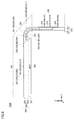
図14は、実施の形態3の変形例2に係る通信装置3000BをX軸方向から平面視した図である。通信装置3000Bは、図12の通信装置3000のアンテナモジュール1300が1300Bに置き換えられた構成である。アンテナモジュール1300Bの構成は、アンテナモジュール1300のアンテナ素子200およびRFIC240がアンテナ素子200CおよびRFIC240Bにそれぞれ置き換えられた構成である。
アンテナ素子200Cにおいては、アンテナ素子200の放射電極203,206,209,212、誘電体基板220、線路導体パターン271~274、接地電極232、ビア導体253,257,261,265、およびビア導体254,258,262,266が、放射電極203C,206C,209C,212C、誘電体基板220C、線路導体パターン271C~274C、接地電極232C、ビア導体253C,257C,261C,265C、およびビア導体254C,258C,262C,266Cにそれぞれ置き換えられている。また、アンテナ素子200Cには、放射電極203D,206D,209D,212D、ビア導体253D,257D,261D,265D、およびビア導体254D,258D,262D,266D、線路導体パターン271D~274D、および接地電極281C~284Cが追加されている。誘電体基板220Cの構成は、誘電体層221,223および部分293が誘電体層221C,223Cおよび部分293Cにそれぞれ置き換えられているとともに、誘電体層224および部分294,295が追加された構成である。これら以外は同様であるため、説明を繰り返さない。
図14に示されるように、誘電体層221C(第1誘電体層)は、フレキシブル素材から形成されている。誘電体層221Cは、部分292,294において屈曲している。平板状の部分295は、部分294に接続し、Y軸方向に延在している。誘電体層224は、部分295に形成されている。誘電体層223Cは、部分293に形成されている。誘電体基板220Cは、実装基板320の端部を巻回するように形成されている。なお、誘電体基板220Cは、一体の誘電体から形成されていてもよい。部分295は、接着層を介して不図示の筐体に固定されてもよい。部分295は、実装基板320に近接するように形成されてもよい。
放射電極203C,206C,209C,212Cは、部分293Cから294に亘って形成され、X軸に沿うように配置されている。放射電極203C,206C,209C,212Cは、部分293CにおいてY軸方向に接地電極232Cに対向している。放射電極203C,206C,209C,212Cは、部分294において部分294の厚み方向に接地電極232Cに対向している。
放射電極203D,206D,209D,212Dは、部分295においてX軸に沿うように配置されている。放射電極203D,206D,209D,212Dの法線方向は、Z軸方向である。
接地電極232Cは、部分291,292,293C,294,295に亘って誘電体層221Cに形成されている。接地電極232Cは、Z軸方向において放射電極203D,206D,209D,212Dと対向している。接地電極232Cは、接地電極231に接続されている。
接地電極281C~284Cは、部分293C,294,295に亘って形成され、X軸に沿うように誘電体層221Cに配置されている。接地電極281C~284Cは、複数のビア導体によって接地電極232Cに接続されている。
線路導体パターン271C~274Cは、部分291,292,293Cに亘って誘電体層221Cに形成されている。線路導体パターン271Cは、接地電極232Cと281との間に形成されている。線路導体パターン272Cは、接地電極232Cと282との間に形成されている。線路導体パターン273Cは、接地電極232Cと283との間に形成されている。線路導体パターン274Cは、接地電極232Cと284との間に形成されている。
ビア導体253C,257C,261C,265Cは、接地電極231を貫通し、線路導体パターン271C~274CとRFIC240Bとをそれぞれ接続している。ビア導体253C,257C,261C,265Cは、接地電極231から絶縁されている。
ビア導体254Cは、線路導体パターン271Cと放射電極203Cとを接続している。ビア導体258Cは、線路導体パターン272Cと放射電極206Cとを接続している。ビア導体262Cは、線路導体パターン273Cと放射電極209Cとを接続している。ビア導体266Cは、線路導体パターン274Cと放射電極212Cとを接続している。
RFIC240Bは、線路導体パターン271C~274Cを介して、放射電極203C,206C,209C,212Cに高周波信号をそれぞれ供給する。RFIC240Bは、線路導体パターン271C~274Cを介して、放射電極203C,206C,209C,212Cから高周波信号をそれぞれ受ける。
線路導体パターン271D~274Dは、部分291,292,293C,294,295に亘って誘電体層221Cに形成されている。線路導体パターン271Dは、接地電極232Cと281との間に形成されているとともに、接地電極232Cと281Cとの間に形成されている。線路導体パターン272Dは、接地電極232Cと282との間に形成されているとともに、接地電極232Cと282Cとの間に形成されている。線路導体パターン273Dは、接地電極232Cと283との間に形成されているとともに、接地電極232Cと283Cとの間に形成されている。線路導体パターン274Dは、接地電極232Cと284との間に形成されているとともに、接地電極232Cと284Cとの間に形成されている。
ビア導体253D,257D,261D,265Dは、接地電極231を貫通し、線路導体パターン271D~274DとRFIC240Bとをそれぞれ接続している。ビア導体253D,257D,261D,265Dは、接地電極231から絶縁されている。
ビア導体254Dは、線路導体パターン271Dと放射電極203Dとを接続している。ビア導体258Dは、線路導体パターン272Dと放射電極206Dとを接続している。ビア導体262Dは、線路導体パターン273Dと放射電極209Dとを接続している。ビア導体266Dは、線路導体パターン274Dと放射電極212Dとを接続している。
RFIC240Bは、線路導体パターン271D~274Dを介して、放射電極203D,206D,209D,212Dに高周波信号をそれぞれ供給する。RFIC240Bは、線路導体パターン271D~274Dを介して、放射電極203D,206D,209D,212Dから高周波信号をそれぞれ受ける。
アンテナ素子200Cにおいては、誘電体基板220Cが部分292,294において屈曲しているため、放射電極201,204,207,210,203D,206D,209D,212Dの法線方向(Z軸方向)、放射電極202,205,208,211の法線方向(部分292の厚み方向)、放射電極203C,206C,209C,212Cの部分293Cにおける法線方向(Y軸方向)、および放射電極203C,206C,209C,212Cの部分294における法線方向(部分294の厚み方向)が互いに異なる。アンテナモジュール1200Bにおいては、複数の放射電極の法線が平行である場合に比べて、励振方向が異なる偏波を有する高周波信号の送信および受信が容易になる。
また、アンテナ素子200Cにおいては、誘電体層221Cがフレキシブル素材から形成されているため、屈曲している部分292,294において発生する応力を低減することができる。部分291、293C、および295において、誘電体基板220Cの表面の平面性を維持することができる。そのため、各放射電極の法線方向が所望の方向からずれることを抑制することができる。その結果、誘電体基板220Cを屈曲することによるアンテナ素子200Cの特性の低下を抑制することができる。
以上、実施の形態3および変形例1,2に係る通信装置によれば、アンテナ素子の放射特性を改善することができる。
今回開示された各実施の形態は、矛盾しない範囲で適宜組み合わされて実施されることも予定されている。今回開示された実施の形態はすべての点で例示であって制限的なものではないと考えられるべきである。本発明の範囲は上記した説明ではなくて請求の範囲によって示され、請求の範囲と均等の意味および範囲内でのすべての変更が含まれることが意図される。
10,100,100A,100B,200,200A,200B,200C アンテナ素子、31A,31D,33A,33D,37 スイッチ、32AR,32DR ローノイズアンプ、32AT,32DT パワーアンプ、34A,34D 減衰器、35A,35D 移相器、36 分波器、38 ミキサ、39 増幅回路、101,102,291~294,292B,293B,293C 部分、110~112,201~212,202B,203B~203D,205B,206B~206D,208B,209B~209D,211B,212B~212D 放射電極、120,120A,220,220B,220C 誘電体基板、121,122,221~224,221B,221C,223B,223C 誘電体層、131,132,231,231B,232,232B,232C,281~284,281B~284B,281C~284C 接地電極、150~152,251~266,251A,251B,252A,252B~266B,253C,253D,254A~256A,254C,254D,257C,257D,258A~260A,258C,258D,261C,261D,262A~264A,262B,262D,265C,265D,266A,266C,266D ビア導体、271~274,271A~274A,271B~274B,271C~274C,271D~274D,275~278 線路導体パターン,320,320A 実装基板,321,322,331,332 コネクタ,1100,1100A,1100B,1200,1200A,1200B,1300,1300A,1300B アンテナモジュール,3000,3000A,3000B 通信装置。
Claims (7)
- 平板状の第1部分、および前記第1部分よりも薄い第2部分を有する誘電体基板と、
前記第1部分に配置された第1接地電極と、
前記第2部分に配置された第2接地電極と、
前記第1接地電極と前記第2接地電極とを接続するビア導体と、
前記第1部分において前記第1部分の第1厚み方向に前記第1接地電極と対向するとともに、前記第2部分において前記第2部分の第2厚み方向に前記第2接地電極と対向するように配置された放射電極とを備え、
前記放射電極と前記第1接地電極との前記第1厚み方向の距離は、前記放射電極と前記第2接地電極との前記第2厚み方向の距離より大きく、
前記放射電極の一部は、前記第2接地電極と対向せず、かつ前記第1接地電極と対向する、アンテナ素子。 - 前記誘電体基板は、一体の誘電体から形成されている、請求項1に記載のアンテナ素子。
- 前記誘電体基板は、
前記第1部分および前記第2部分に亘って形成された第1誘電体層と、
前記第1部分に形成された第2誘電体層とを含み、
前記放射電極および前記第2接地電極は、前記第1誘電体層に配置され、
前記第1接地電極は、前記第2誘電体層に配置されている、請求項1に記載のアンテナ素子。 - 前記誘電体基板は、前記第2部分において屈曲している、請求項2または3に記載のアンテナ素子。
- 前記第2部分は、柔軟性を有する素材から形成されている、請求項4に記載のアンテナ素子。
- 請求項1~5のいずれか1項に記載のアンテナ素子と、
前記アンテナ素子に高周波信号を供給する高周波素子とを備える、アンテナモジュール。 - 請求項6に記載のアンテナモジュールを備える、通信装置。
Priority Applications (1)
| Application Number | Priority Date | Filing Date | Title |
|---|---|---|---|
| US17/169,726 US11881640B2 (en) | 2018-08-09 | 2021-02-08 | Antenna element, antenna module, and communication device |
Applications Claiming Priority (2)
| Application Number | Priority Date | Filing Date | Title |
|---|---|---|---|
| JP2018-150512 | 2018-08-09 | ||
| JP2018150512 | 2018-08-09 |
Related Child Applications (1)
| Application Number | Title | Priority Date | Filing Date |
|---|---|---|---|
| US17/169,726 Continuation US11881640B2 (en) | 2018-08-09 | 2021-02-08 | Antenna element, antenna module, and communication device |
Publications (1)
| Publication Number | Publication Date |
|---|---|
| WO2020031876A1 true WO2020031876A1 (ja) | 2020-02-13 |
Family
ID=69414686
Family Applications (1)
| Application Number | Title | Priority Date | Filing Date |
|---|---|---|---|
| PCT/JP2019/030419 WO2020031876A1 (ja) | 2018-08-09 | 2019-08-02 | アンテナ素子、アンテナモジュールおよび通信装置 |
Country Status (2)
| Country | Link |
|---|---|
| US (1) | US11881640B2 (ja) |
| WO (1) | WO2020031876A1 (ja) |
Families Citing this family (1)
| Publication number | Priority date | Publication date | Assignee | Title |
|---|---|---|---|---|
| KR102400030B1 (ko) * | 2020-11-18 | 2022-05-18 | 동우 화인켐 주식회사 | 안테나 패키지 및 이를 포함하는 화상 표시 장치 |
Citations (5)
| Publication number | Priority date | Publication date | Assignee | Title |
|---|---|---|---|---|
| JPH0964636A (ja) * | 1995-08-21 | 1997-03-07 | Matsushita Electric Ind Co Ltd | 平面アンテナ |
| WO2006011459A1 (ja) * | 2004-07-28 | 2006-02-02 | Osaka University | パッチアンテナ及びパッチアンテナの製造方法 |
| JP2007013327A (ja) * | 2005-06-28 | 2007-01-18 | Tdk Corp | アンテナ装置 |
| JP2009038696A (ja) * | 2007-08-03 | 2009-02-19 | Toyota Central R&D Labs Inc | アンテナ付き集積回路パッケージ |
| US20130249740A1 (en) * | 2012-03-23 | 2013-09-26 | Apple Inc. | Flexible Printed Circuit Structures |
Family Cites Families (4)
| Publication number | Priority date | Publication date | Assignee | Title |
|---|---|---|---|---|
| JP2003332830A (ja) | 2002-05-09 | 2003-11-21 | Matsushita Electric Ind Co Ltd | 平面アンテナ、無線端末装置および無線基地局 |
| KR100758998B1 (ko) * | 2006-05-24 | 2007-09-17 | 삼성전자주식회사 | 근거리 통신용 패치 안테나 |
| WO2012081288A1 (ja) | 2010-12-17 | 2012-06-21 | 株式会社村田製作所 | 高周波用パッケージ |
| JP6339319B2 (ja) | 2013-04-16 | 2018-06-06 | 日本ピラー工業株式会社 | マイクロストリップアンテナ及び携帯型端末 |
-
2019
- 2019-08-02 WO PCT/JP2019/030419 patent/WO2020031876A1/ja active Application Filing
-
2021
- 2021-02-08 US US17/169,726 patent/US11881640B2/en active Active
Patent Citations (5)
| Publication number | Priority date | Publication date | Assignee | Title |
|---|---|---|---|---|
| JPH0964636A (ja) * | 1995-08-21 | 1997-03-07 | Matsushita Electric Ind Co Ltd | 平面アンテナ |
| WO2006011459A1 (ja) * | 2004-07-28 | 2006-02-02 | Osaka University | パッチアンテナ及びパッチアンテナの製造方法 |
| JP2007013327A (ja) * | 2005-06-28 | 2007-01-18 | Tdk Corp | アンテナ装置 |
| JP2009038696A (ja) * | 2007-08-03 | 2009-02-19 | Toyota Central R&D Labs Inc | アンテナ付き集積回路パッケージ |
| US20130249740A1 (en) * | 2012-03-23 | 2013-09-26 | Apple Inc. | Flexible Printed Circuit Structures |
Also Published As
| Publication number | Publication date |
|---|---|
| US11881640B2 (en) | 2024-01-23 |
| US20210167506A1 (en) | 2021-06-03 |
Similar Documents
| Publication | Publication Date | Title |
|---|---|---|
| JP6930591B2 (ja) | アンテナモジュールおよび通信装置 | |
| WO2018230475A1 (ja) | アンテナモジュールおよび通信装置 | |
| JP6874829B2 (ja) | アンテナモジュールおよび通信装置 | |
| CN211789514U (zh) | 天线模块以及天线机器 | |
| WO2020261806A1 (ja) | アンテナモジュールおよびそれを搭載した通信装置 | |
| JP7047918B2 (ja) | アンテナモジュール | |
| JP7014287B2 (ja) | アンテナモジュールおよびそれを搭載した通信装置 | |
| US11936096B2 (en) | Wiring substrate, antenna module, and communication device | |
| CN110933957B (zh) | 天线装置、天线模块以及在该天线模块中使用的电路基板 | |
| WO2020145392A1 (ja) | アンテナモジュールおよびそれを搭載した通信装置 | |
| JP6760541B2 (ja) | アンテナモジュールおよびそれを搭載した通信装置 | |
| JP6741189B1 (ja) | アンテナ素子、アンテナモジュールおよび通信装置 | |
| JPWO2019130771A1 (ja) | アンテナアレイおよびアンテナモジュール | |
| WO2020261920A1 (ja) | フレキシブル基板、およびフレキシブル基板を備えるアンテナモジュール | |
| WO2020031876A1 (ja) | アンテナ素子、アンテナモジュールおよび通信装置 | |
| JP6798656B1 (ja) | アンテナモジュールおよびそれを搭載した通信装置 | |
| JP6590132B1 (ja) | アンテナ装置、アンテナモジュール、およびそれに用いられる回路基板 | |
| WO2020031777A1 (ja) | アンテナ素子、アンテナモジュールおよび通信装置 | |
| JP7059385B2 (ja) | アンテナモジュールおよびそれを搭載した通信装置 | |
| WO2023120357A1 (ja) | アンテナモジュールおよび通信装置 | |
| WO2022230427A1 (ja) | アンテナ装置 | |
| WO2023032805A1 (ja) | アンテナ装置、アンテナモジュールおよび通信装置 | |
| WO2023037806A1 (ja) | アンテナモジュールおよびそれを搭載した通信装置 | |
| WO2020162437A1 (ja) | アンテナモジュールおよび通信装置 | |
| WO2023095643A1 (ja) | アンテナモジュール、およびそれを搭載した通信装置 |
Legal Events
| Date | Code | Title | Description |
|---|---|---|---|
| 121 | Ep: the epo has been informed by wipo that ep was designated in this application |
Ref document number: 19846489 Country of ref document: EP Kind code of ref document: A1 |
|
| NENP | Non-entry into the national phase |
Ref country code: DE |
|
| 122 | Ep: pct application non-entry in european phase |
Ref document number: 19846489 Country of ref document: EP Kind code of ref document: A1 |
|
| NENP | Non-entry into the national phase |
Ref country code: JP |