WO2020026732A1 - Structure de circuit - Google Patents
Structure de circuit Download PDFInfo
- Publication number
- WO2020026732A1 WO2020026732A1 PCT/JP2019/027277 JP2019027277W WO2020026732A1 WO 2020026732 A1 WO2020026732 A1 WO 2020026732A1 JP 2019027277 W JP2019027277 W JP 2019027277W WO 2020026732 A1 WO2020026732 A1 WO 2020026732A1
- Authority
- WO
- WIPO (PCT)
- Prior art keywords
- circuit board
- opening
- bus bar
- fet
- conductive
- Prior art date
Links
Images


Classifications
-
- G—PHYSICS
- G01—MEASURING; TESTING
- G01K—MEASURING TEMPERATURE; MEASURING QUANTITY OF HEAT; THERMALLY-SENSITIVE ELEMENTS NOT OTHERWISE PROVIDED FOR
- G01K1/00—Details of thermometers not specially adapted for particular types of thermometer
- G01K1/16—Special arrangements for conducting heat from the object to the sensitive element
-
- G—PHYSICS
- G01—MEASURING; TESTING
- G01K—MEASURING TEMPERATURE; MEASURING QUANTITY OF HEAT; THERMALLY-SENSITIVE ELEMENTS NOT OTHERWISE PROVIDED FOR
- G01K7/00—Measuring temperature based on the use of electric or magnetic elements directly sensitive to heat ; Power supply therefor, e.g. using thermoelectric elements
- G01K7/01—Measuring temperature based on the use of electric or magnetic elements directly sensitive to heat ; Power supply therefor, e.g. using thermoelectric elements using semiconducting elements having PN junctions
-
- G—PHYSICS
- G01—MEASURING; TESTING
- G01K—MEASURING TEMPERATURE; MEASURING QUANTITY OF HEAT; THERMALLY-SENSITIVE ELEMENTS NOT OTHERWISE PROVIDED FOR
- G01K1/00—Details of thermometers not specially adapted for particular types of thermometer
- G01K1/14—Supports; Fastening devices; Arrangements for mounting thermometers in particular locations
-
- H—ELECTRICITY
- H01—ELECTRIC ELEMENTS
- H01L—SEMICONDUCTOR DEVICES NOT COVERED BY CLASS H10
- H01L23/00—Details of semiconductor or other solid state devices
- H01L23/58—Structural electrical arrangements for semiconductor devices not otherwise provided for, e.g. in combination with batteries
-
- H—ELECTRICITY
- H05—ELECTRIC TECHNIQUES NOT OTHERWISE PROVIDED FOR
- H05K—PRINTED CIRCUITS; CASINGS OR CONSTRUCTIONAL DETAILS OF ELECTRIC APPARATUS; MANUFACTURE OF ASSEMBLAGES OF ELECTRICAL COMPONENTS
- H05K1/00—Printed circuits
- H05K1/18—Printed circuits structurally associated with non-printed electric components
- H05K1/181—Printed circuits structurally associated with non-printed electric components associated with surface mounted components
-
- H—ELECTRICITY
- H05—ELECTRIC TECHNIQUES NOT OTHERWISE PROVIDED FOR
- H05K—PRINTED CIRCUITS; CASINGS OR CONSTRUCTIONAL DETAILS OF ELECTRIC APPARATUS; MANUFACTURE OF ASSEMBLAGES OF ELECTRICAL COMPONENTS
- H05K1/00—Printed circuits
- H05K1/18—Printed circuits structurally associated with non-printed electric components
- H05K1/189—Printed circuits structurally associated with non-printed electric components characterised by the use of a flexible or folded printed circuit
-
- H—ELECTRICITY
- H05—ELECTRIC TECHNIQUES NOT OTHERWISE PROVIDED FOR
- H05K—PRINTED CIRCUITS; CASINGS OR CONSTRUCTIONAL DETAILS OF ELECTRIC APPARATUS; MANUFACTURE OF ASSEMBLAGES OF ELECTRICAL COMPONENTS
- H05K3/00—Apparatus or processes for manufacturing printed circuits
- H05K3/30—Assembling printed circuits with electric components, e.g. with resistor
- H05K3/32—Assembling printed circuits with electric components, e.g. with resistor electrically connecting electric components or wires to printed circuits
- H05K3/34—Assembling printed circuits with electric components, e.g. with resistor electrically connecting electric components or wires to printed circuits by soldering
- H05K3/3405—Edge mounted components, e.g. terminals
-
- H—ELECTRICITY
- H05—ELECTRIC TECHNIQUES NOT OTHERWISE PROVIDED FOR
- H05K—PRINTED CIRCUITS; CASINGS OR CONSTRUCTIONAL DETAILS OF ELECTRIC APPARATUS; MANUFACTURE OF ASSEMBLAGES OF ELECTRICAL COMPONENTS
- H05K7/00—Constructional details common to different types of electric apparatus
- H05K7/02—Arrangements of circuit components or wiring on supporting structure
- H05K7/06—Arrangements of circuit components or wiring on supporting structure on insulating boards, e.g. wiring harnesses
-
- H—ELECTRICITY
- H05—ELECTRIC TECHNIQUES NOT OTHERWISE PROVIDED FOR
- H05K—PRINTED CIRCUITS; CASINGS OR CONSTRUCTIONAL DETAILS OF ELECTRIC APPARATUS; MANUFACTURE OF ASSEMBLAGES OF ELECTRICAL COMPONENTS
- H05K7/00—Constructional details common to different types of electric apparatus
- H05K7/14—Mounting supporting structure in casing or on frame or rack
- H05K7/1422—Printed circuit boards receptacles, e.g. stacked structures, electronic circuit modules or box like frames
- H05K7/1427—Housings
- H05K7/1432—Housings specially adapted for power drive units or power converters
- H05K7/14329—Housings specially adapted for power drive units or power converters specially adapted for the configuration of power bus bars
-
- H—ELECTRICITY
- H05—ELECTRIC TECHNIQUES NOT OTHERWISE PROVIDED FOR
- H05K—PRINTED CIRCUITS; CASINGS OR CONSTRUCTIONAL DETAILS OF ELECTRIC APPARATUS; MANUFACTURE OF ASSEMBLAGES OF ELECTRICAL COMPONENTS
- H05K1/00—Printed circuits
- H05K1/02—Details
- H05K1/0201—Thermal arrangements, e.g. for cooling, heating or preventing overheating
-
- H—ELECTRICITY
- H05—ELECTRIC TECHNIQUES NOT OTHERWISE PROVIDED FOR
- H05K—PRINTED CIRCUITS; CASINGS OR CONSTRUCTIONAL DETAILS OF ELECTRIC APPARATUS; MANUFACTURE OF ASSEMBLAGES OF ELECTRICAL COMPONENTS
- H05K2201/00—Indexing scheme relating to printed circuits covered by H05K1/00
- H05K2201/05—Flexible printed circuits [FPCs]
- H05K2201/056—Folded around rigid support or component
-
- H—ELECTRICITY
- H05—ELECTRIC TECHNIQUES NOT OTHERWISE PROVIDED FOR
- H05K—PRINTED CIRCUITS; CASINGS OR CONSTRUCTIONAL DETAILS OF ELECTRIC APPARATUS; MANUFACTURE OF ASSEMBLAGES OF ELECTRICAL COMPONENTS
- H05K2201/00—Indexing scheme relating to printed circuits covered by H05K1/00
- H05K2201/10—Details of components or other objects attached to or integrated in a printed circuit board
- H05K2201/10007—Types of components
- H05K2201/10166—Transistor
-
- H—ELECTRICITY
- H05—ELECTRIC TECHNIQUES NOT OTHERWISE PROVIDED FOR
- H05K—PRINTED CIRCUITS; CASINGS OR CONSTRUCTIONAL DETAILS OF ELECTRIC APPARATUS; MANUFACTURE OF ASSEMBLAGES OF ELECTRICAL COMPONENTS
- H05K2201/00—Indexing scheme relating to printed circuits covered by H05K1/00
- H05K2201/10—Details of components or other objects attached to or integrated in a printed circuit board
- H05K2201/10007—Types of components
- H05K2201/10219—Thermoelectric component
-
- H—ELECTRICITY
- H05—ELECTRIC TECHNIQUES NOT OTHERWISE PROVIDED FOR
- H05K—PRINTED CIRCUITS; CASINGS OR CONSTRUCTIONAL DETAILS OF ELECTRIC APPARATUS; MANUFACTURE OF ASSEMBLAGES OF ELECTRICAL COMPONENTS
- H05K2201/00—Indexing scheme relating to printed circuits covered by H05K1/00
- H05K2201/10—Details of components or other objects attached to or integrated in a printed circuit board
- H05K2201/10227—Other objects, e.g. metallic pieces
- H05K2201/10272—Busbars, i.e. thick metal bars mounted on the PCB as high-current conductors
Definitions
- the present invention relates to a circuit component.
- This application claims the priority based on Japanese Patent Application No. 2018-144347 filed on Jul. 31, 2018, and incorporates all the contents described in the Japanese application.
- a circuit component that controls energization related to power supply from a power supply to a load is mounted between a power supply and a load in a vehicle.
- the circuit component includes a switching element, and further includes a control circuit that controls on / off of the switching element.
- the switching element turns on and off based on a signal input from the control circuit.
- the circuit component controls the energization by turning on and off the switching elements.
- the temperature of the switching element may be measured by a temperature measuring device in some cases.
- a temperature measuring device thermoistor
- a switching element power MOSFET
- a conductive portion to which a switching element to be measured is attached, and a temperature detector (temperature).
- the conductive part to which the detection element is connected is formed integrally with the circuit board.
- a circuit structure includes a circuit board, a switching element mounted on one surface of the circuit board, a folded portion extending from a peripheral portion of the circuit board, and being folded toward the one surface. And a temperature measuring device mounted on the folded portion and in contact with the switching element.
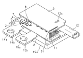
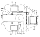
- FIG. 1 is an external perspective view of a circuit structure according to the embodiment.
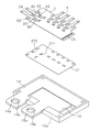
- FIG. 2 is a perspective view of a circuit structure showing a state in which a lid is removed.
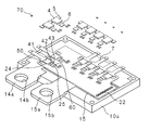
- FIG. 3 is a perspective view showing a mounting mode of the FET.
- FIG. 4 is a perspective view showing a state where no circuit board is mounted.
- FIG. 5 is a perspective view illustrating mounting of the FET.
- FIG. 6 is a partially enlarged plan view showing the first conductive part and the second conductive part.
- FIG. 7 is a partially enlarged plan view showing a mounting mode of the thermistor.
- FIG. 8 is a sectional view taken along line VIII-VIII in FIG.
- a heat radiator having a large heat capacity is used in the circuit structure.
- heat conduction from the switching element to the circuit board is weakened, and the ambient temperature of the temperature detector does not increase.
- the temperature of the switching element cannot be measured satisfactorily, and abnormal heat generation may not be detected properly.
- An object of the present invention is to provide a circuit structure that can measure the temperature of a switching element satisfactorily.
- the temperature of the switching element can be satisfactorily measured.
- a circuit structure includes a circuit board, a switching element mounted on one surface of the circuit board, a folded portion extending from a peripheral edge of the circuit board, and being folded toward the one surface. And a temperature measuring device mounted on the folded portion and in contact with the switching element.
- the distance between the temperature measuring device and the switching element is short, and the temperature of the switching element can be measured favorably.
- the circuit structure according to one embodiment of the present invention includes a plurality of the switching elements, the folded portions, and the temperature measuring devices.
- the temperatures of the plurality of switching elements can be measured separately.
- a fixing portion is provided between the temperature measuring device and the switching element.
- the temperature measuring device can be fixed to the fixing portion satisfactorily.
- the fixing portion is thermosetting.
- the temperature measuring device can be satisfactorily fixed to the fixing portion by embedding the temperature measuring device in the fixing portion before the thermosetting and then performing the heat setting.
- a circuit structure includes an input-side bus bar facing the other surface of the circuit board and receiving power, and an output-side bus bar facing the other surface of the circuit board and receiving power. And a conductive portion provided on the circuit board and connecting an input terminal and an output terminal of the switching element to the input side bus bar and the output side bus bar, respectively.
- the power input from the input-side bus bar and output from the output-side bus bar can be turned on and off by the switching element.
- FIG. 1 is an external perspective view of a circuit structure according to the embodiment.
- the circuit structure 1 is disposed on a power supply path between a power supply such as a battery included in a vehicle and a load such as a lamp, a wiper, or a motor.
- a power supply such as a battery included in a vehicle
- a load such as a lamp, a wiper, or a motor.
- the circuit structure 1 includes the housing 10.
- the housing 10 has a rectangular parallelepiped shape, and includes a rectangular flat plate-shaped main body 10a and a lid 10b that covers one surface of the main body 10a over the entire surface.
- FIG. 2 is a perspective view of the circuit structure showing a state in which the cover 10b is removed.
- the circuit structure 1 includes a circuit board 2 and a control board 3.
- the circuit board 2 is, for example, an FPC (Flexible Printed Circuits) or the like.
- the circuit board 2 is placed with one surface facing the main body 10a.
- the circuit board 2 is mounted with electronic components such as a field effect transistor (FET) and a conductive piece, which will be described later.
- FET field effect transistor
- the control board 3 has a rectangular plate shape, and is arranged so that one surface faces the circuit board and the longitudinal direction is along the longitudinal direction of the circuit board 2.
- a control circuit including electronic components such as a resistor, a coil, a capacitor, and a diode and a wiring pattern for electrically connecting these electronic components is provided.
- a bar-shaped connection connector 11 is provided upright on one short side of the circuit board 2.
- the circuit board 2 is connected to the control board 3 via the connector 11.
- the connector 12 has a cylindrical outer shape, and a plurality of rod-shaped terminal portions 12a are provided inside the connector 12. One end of the terminal portion 12a is connected to an externally provided ECU (Electronic Control Unit) via a signal line (not shown). The other end of each terminal 12 a of the connector 12 is connected to a wiring pattern of the control board 3.
- ECU Electronic Control Unit
- the connector 12 projects from the cover 10b as shown in FIG.
- FIG. 3 is a perspective view showing a mounting mode of the FET.
- the circuit structure 1 includes a plurality of FETs 4 (six in the figure), a plurality of first conductive pieces 5 (eight in the figure), and a plurality of second conductive pieces 6 (six in the figure). Note that the number of the FETs 4, the first conductive pieces 5, and the second conductive pieces 6 are not limited to the illustrated numbers.
- two FETs 4 are arranged along the other short side opposite to the one short side, and four FETs 4 are arranged side by side along the one long side. I have.
- a plurality of through holes 22 to which the connector 11 is connected are arranged in parallel.
- the first conductive pieces 5 are arranged so as to sandwich each FET 4, and three are arranged along the other short side of the circuit board 2 and five along one long side.
- the second conductive pieces 6 are arranged two along the other short side of the circuit board 2 and four along the one long side.
- the second conductive pieces 6 are provided so as to correspond to the FETs 4 respectively, and are located inside the FETs 4.
- a plurality of chip components are arranged around the second conductive piece 6.
- the first conductive piece 5 and the second conductive piece 6 are preferably copper chips having excellent conductivity and heat conductivity.
- FIG. 4 is a perspective view showing a state where the circuit board 2 is not mounted.
- FIG. 5 is a perspective view illustrating mounting of the FET 4.
- FIG. 6 is a partially enlarged plan view showing the first conductive portion and the second conductive portion.
- a plate-shaped input bus bar 14 and an output bus bar 15 are provided on one surface of the main body 10a.
- the input-side bus bar 14 has an L-shape in plan view, and the L-shaped linear portions are respectively positioned along the long side and the short side of the main body 10a.
- An input terminal 14a is continuously provided at one end of the input-side bus bar 14, and protrudes from the main body 10a.
- the output-side bus bar 15 has a rectangular shape and is arranged at the center of one surface of the main body 10a.
- the output-side bus bar 15 is arranged at a predetermined distance from the input-side bus bar 14 such that the longitudinal direction is along the longitudinal direction of the main body 10a.
- an output terminal portion 15a is continuously provided at the center of the long side of the input-side bus bar 14, and protrudes from the main body portion 10a.
- the input-side bus bar 14 and the output-side bus bar 15, the input terminal portion 14a, and the output terminal portion 15a are, for example, formed of a bus bar member having a plate thickness of 2 mm and a nickel plated surface.
- the input terminal portion 14a and the output terminal portion 15a are provided with through holes 14b, 15b penetrating in the thickness direction, respectively, and are connected to a power source and a load by bolts (not shown) inserted into the through holes 14b, 15b. You.
- the input terminal 14a is connected to the power supply, and the output terminal 15a is connected to the load.
- the main body 10a is manufactured by insert molding using an insulating resin material such as a phenol resin and a glass epoxy resin.
- the resin molded body formed of the insulating resin material is integrated with the input terminal portion 14a, the output terminal portion 15a, the input side bus bar 14, and the output side bus bar 15 by being joined thereto. Further, the resin molded body is arranged between the input terminal portion 14a and the output terminal portion 15a and between the input side bus bar 14 and the output side bus bar 15 to insulate them.
- the circuit board 2 is bonded to the main body 10a by a rectangular heat conductive and insulating adhesive sheet 21 as shown in FIG.
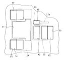
- a first opening 41, a second opening 42, and a third opening 43 are provided through the circuit board 2 at positions corresponding to the respective FETs 4.
- the second opening 42 and the third opening 43 are located inside the first opening 41 on the circuit board 2 and are arranged in the longitudinal direction or the short direction.
- the first opening 41 is larger than the second opening 42 and the third opening 43, and the second opening 42 is larger than the third opening 43.
- the circuit board 2 has a fourth opening 50 at a position corresponding to each first conductive piece 5. Further, a fifth opening 60 is provided at a position corresponding to each second conductive piece 6. The fifth opening 60 is positioned so as to sandwich the second opening 42 with the first opening 41.
- the rectangular first conductive portion 24 is provided at a position corresponding to the first opening 41 and the fourth opening 50.
- the first conductive portion 24 is exposed from the entire first opening 41 to the other surface, and is exposed to the other surface in an inner half of the fourth opening 50. If the first conductive portion is exposed as described above, the first conductive portion may be provided in an L shape so as to correspond to all the first openings 41 and the fourth openings 50, or the first opening may be provided. It may be provided for each of the portion 41 and the fourth opening 50.
- a rectangular second conductive portion 25 is provided at a position corresponding to the second opening 42 and the fifth opening 60.
- the second conductive portion 25 is exposed from the entire second opening 42 to the other surface, and is exposed from the outer half of the fifth opening 60 to the other surface.
- a land 26 is provided at a position corresponding to the third opening 43, and is exposed from the entire third opening 43 to the other surface.
- a connection portion 22a for electrically connecting the land portion 26 and the through hole 22 is provided on one surface of the circuit board 2.
- the first conductive part 24, the second conductive part 25, the land part 26, and the connection part 22a are formed of, for example, copper foil.
- a first hole 210 and a second hole 211 are formed in the adhesive sheet 21 at positions corresponding to the fourth opening 50 and the fifth opening 60 of the circuit board 2.
- the first hole 210 corresponds to the outer half of the fourth opening 50
- the second hole 211 corresponds to the inner half of the fifth opening 60.
- the circuit board 2 and the adhesive sheet 21 have a surface on which the circuit pattern of the circuit board 2 including the first conductive portion 24, the second conductive portion 25, the land portion 26, and the connection portion 22a is formed on the adhesive sheet 21 side. It is arranged so as to be located on one surface of the main body 10a.
- the first hole 210 continues to the fourth opening 50 and does not overlap the first conductive part 24. Further, the second hole 211 is continuous with the fifth opening 60 and does not overlap the second conductive portion 25.
- a part of the input-side bus bar 14 is exposed from the fourth opening 50 and the first hole 210, and a part of the output-side bus bar 15 is exposed from the fifth opening 60 and the second hole 211. It is exposed.
- the circuit board 2 is formed by, for example, using polyimide as a base member, forming a pattern including conductive parts and the like on one surface by etching, and attaching an insulating cover film to the pattern.
- a pattern including conductive parts and the like on one surface by etching, and attaching an insulating cover film to the pattern.
- the first conductive part 24, the second conductive part 25, the land part 26, and the connection part 22a for example, a 35- ⁇ m copper foil is used.
- Each conductive piece is made of, for example, 0.2 mm to 0.5 mm made of pure copper or a copper alloy, and has a surface plated with tin, nickel, or the like.
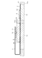
- FIG. 7 is a partially enlarged plan view showing a mounting mode of the thermistor 70.
- FIG. 8 is a sectional view taken along line VIII-VIII in FIG.
- the FET 4 has a rectangular parallelepiped shape, and has four drain terminals 44 protruding from one side and two sides connected to the one side, and one gate protruding from the side opposite to the one side. A terminal 45 and three source terminals 46 are provided.
- the FET 4 is disposed so as to straddle the first opening 41 to the third opening 43.
- Each drain terminal 44 is soldered to the first conductive part 24 at the first opening 41
- the gate terminal 45 is soldered to the land 26 at the third opening 43
- the source terminal 46 is soldered to the land 26 at the second opening 42. It is soldered to the two conductive parts 25.
- the first conductive piece 5 is disposed in the fourth opening 50 so as to straddle the input side bus bar 14 and the first conductive part 24, and is connected to these by solder.
- the second conductive piece 6 is disposed in the fifth opening 60 so as to straddle the output-side bus bar 15 and the second conductive portion 25, and is connected to these by solder.
- the adhesive sheet 21 preferably contains a heat conductive filler, for example, and is preferably a sheet using an acrylic or silicone-based highly heat-resistant adhesive.
- a heat conductive filler for example, and is preferably a sheet using an acrylic or silicone-based highly heat-resistant adhesive.
- the circuit board 2 is provided with the folded portion 7 at a position corresponding to each of the first openings 41.
- a thermistor 70 is attached to the extension end of the folded portion 7.
- the folded portion 7 extends vertically from the short side or the long side of the circuit board 2, and is bent such that the extended end comes into contact with each FET 4. 4 and 5 show a state before the folding unit 7 is folded.
- the temperature of each FET 4 can be individually measured by the thermistor 70.
- the thermistor 70 is connected to the through hole 22 via a circuit pattern (not shown) formed by a copper foil of the circuit board 2.
- the thermistor 70 is an example of a temperature measuring device, and another temperature measuring device such as a semiconductor temperature sensor may be used instead of the thermistor 70.
- the folded portion 7 of the circuit board 2 is bent at the base end side after the FET 4 is attached, and the extended end portion is in contact with the top surface of the FET 4.
- the thermistor 70 provided at the extension end of the folded portion 7 is sandwiched between the folded portion 7 and the FET 4 and is fixed to the top surface of the FET 4 by being embedded in the fixing portion 71 located between the folded portion 7 and the FET 4. Have been.
- the fixing portion 71 is formed of, for example, a thermosetting silicone composition containing a heat conductive filler.
- a gel-like fixing portion 71 before thermosetting is applied to the top surface of the FET 4, and the folded portion 7 is bent to embed the thermistor 70 in the fixing portion 71. Thereafter, the thermistor 70 is fixed to the FET 4 by thermally curing the fixing portion 71.
- the gate terminal 45 of the FET 4 is connected to the control board 3 via the land 26, the connecting portion 22a, the through hole 22, and the connector 11.
- a signal from the control board 3 based on a signal from the external ECU is input to the FET 4.
- On / off of the FET 4 is switched by a signal from the control board 3.
- a predetermined voltage is applied to the gate terminal 45, the drain terminal 44 and the source terminal 46 conduct, and the FET 4 turns on.
- the drain terminal 44 of the FET 4 is connected to the input side bus bar 14 via the first conductive portion 24 and the first conductive piece 5.
- the source terminal 46 of the FET 4 is connected to the output-side bus bar 15 via the second conductive portion 25 and the second conductive piece 6.
- the FET 4 when the FET 4 is turned on by the input of a signal from the control board 3, the power supplied from the input terminal portion 14 a depends on the first conductive portion 24, the first conductive piece 5, the drain terminal 44 and the source terminal 46 of the FET 4.
- the signal is output from the output terminal 15 a via the output-side bus bar 15 via the second conductive portion 25 and the second conductive piece 6.
- power is supplied from the power supply to the load via the circuit structure 1.
- the thermistor 70 is further connected to the control board 3 via the circuit pattern of the circuit board 2, the through hole 22, and the connector 11. Thus, a signal relating to the temperature measured by the thermistor 70 can be input to the control board 3. Therefore, the control board 3 can detect whether the FET 4 is overheated based on the signal from the thermistor 70. When the FET 4 is overheated, the control board 3 can turn off the FET 4 and prevent overheating of the FET 4.
- the thermistor 70 is fixed to the top surface of the FET 4, the distance from the FET 4 is shorter than in the case of measuring the peripheral temperature of the FET 4, and the temperature of the FET 4 can be measured better. can do. Thus, when the temperature of the FET 4 rises and becomes equal to or higher than a predetermined threshold temperature, it is possible to determine whether the FET 4 is overheated. Further, since the thermistor 70 is buried and fixed in the fixing portion 71, it can be fixed more reliably.
Landscapes
- Engineering & Computer Science (AREA)
- Microelectronics & Electronic Packaging (AREA)
- Physics & Mathematics (AREA)
- General Physics & Mathematics (AREA)
- Manufacturing & Machinery (AREA)
- Condensed Matter Physics & Semiconductors (AREA)
- Computer Hardware Design (AREA)
- Power Engineering (AREA)
- Connection Or Junction Boxes (AREA)
- Measuring Temperature Or Quantity Of Heat (AREA)
- Structure Of Printed Boards (AREA)
Abstract
L'invention concerne une structure de circuit qui comprend une carte de circuit imprimé, un élément de commutation monté sur une surface de la carte de circuit imprimé, une section pliée s'étendant à partir d'une section périphérique de la carte de circuit imprimé et repliée vers le côté de surface, et un instrument de mesure de température monté sur la section pliée et en contact avec l'élément de commutation.
Priority Applications (2)
| Application Number | Priority Date | Filing Date | Title |
|---|---|---|---|
| US17/262,511 US11898915B2 (en) | 2018-07-31 | 2019-07-10 | Circuit assembly |
| CN201980046854.4A CN112514064A (zh) | 2018-07-31 | 2019-07-10 | 电路结构体 |
Applications Claiming Priority (2)
| Application Number | Priority Date | Filing Date | Title |
|---|---|---|---|
| JP2018-144347 | 2018-07-31 | ||
| JP2018144347A JP7044007B2 (ja) | 2018-07-31 | 2018-07-31 | 回路構成体 |
Publications (1)
| Publication Number | Publication Date |
|---|---|
| WO2020026732A1 true WO2020026732A1 (fr) | 2020-02-06 |
Family
ID=69230964
Family Applications (1)
| Application Number | Title | Priority Date | Filing Date |
|---|---|---|---|
| PCT/JP2019/027277 WO2020026732A1 (fr) | 2018-07-31 | 2019-07-10 | Structure de circuit |
Country Status (4)
| Country | Link |
|---|---|
| US (1) | US11898915B2 (fr) |
| JP (1) | JP7044007B2 (fr) |
| CN (1) | CN112514064A (fr) |
| WO (1) | WO2020026732A1 (fr) |
Cited By (1)
| Publication number | Priority date | Publication date | Assignee | Title |
|---|---|---|---|---|
| FR3127339A1 (fr) * | 2021-09-20 | 2023-03-24 | Valeo Systemes De Controle Moteur | Module électronique avec élément de connexion amélioré |
Citations (3)
| Publication number | Priority date | Publication date | Assignee | Title |
|---|---|---|---|---|
| JPH09289281A (ja) * | 1996-04-23 | 1997-11-04 | Kokusai Electric Co Ltd | トランジスタの温度検出回路 |
| WO2001015228A1 (fr) * | 1999-08-19 | 2001-03-01 | Seiko Epson Corporation | Panneau de cablage, procede de fabrication d'un panneau de cablage, dispositif semiconducteur, procede de fabrication d'un dispositif semiconducteur, carte a circuit imprime et appareil electronique |
| JP2004253759A (ja) * | 2002-12-24 | 2004-09-09 | Auto Network Gijutsu Kenkyusho:Kk | 制御回路基板及び回路構成体 |
Family Cites Families (18)
| Publication number | Priority date | Publication date | Assignee | Title |
|---|---|---|---|---|
| JPH10188713A (ja) * | 1996-12-20 | 1998-07-21 | Nakamura Denki Seisakusho:Kk | 耐圧防爆構造温度スイッチ |
| JP4256256B2 (ja) * | 2001-06-18 | 2009-04-22 | ギブン イメージング リミテッド | 硬質の区域および軟質の区域を有する回路基板を備えた生体内センシング装置 |
| JP3956886B2 (ja) * | 2002-11-22 | 2007-08-08 | 株式会社豊田自動織機 | 半導体モジュールおよび半導体モジュール用リード |
| JP2004327839A (ja) * | 2003-04-25 | 2004-11-18 | Sony Corp | 電子機器 |
| JP2005150154A (ja) * | 2003-11-11 | 2005-06-09 | Sharp Corp | 半導体モジュールとその実装方法 |
| JP2005203674A (ja) * | 2004-01-19 | 2005-07-28 | Nitto Denko Corp | 電子部品内蔵基板の製造方法 |
| JP4285339B2 (ja) * | 2004-06-15 | 2009-06-24 | パナソニック株式会社 | 回路モジュールおよび回路モジュールの製造方法 |
| JP4254725B2 (ja) | 2005-02-23 | 2009-04-15 | ヤマハ株式会社 | プリント基板、及び温度検出素子の実装構造 |
| JP2007266240A (ja) * | 2006-03-28 | 2007-10-11 | Fujitsu Ltd | 電子装置及びそれを有する電子機器 |
| JP2010200982A (ja) * | 2009-03-04 | 2010-09-16 | Panasonic Corp | 可撓性センサモジュール |
| JP2011035345A (ja) * | 2009-08-06 | 2011-02-17 | Fujitsu Ltd | 半導体素子モジュール、電子回路ユニット、電子デバイス、及び、半導体素子モジュールの製造方法 |
| EP2333831B1 (fr) * | 2009-12-10 | 2016-03-02 | ST-Ericsson SA | Méthode d'emballage d'un dispositif électronique |
| KR20120079742A (ko) * | 2011-01-05 | 2012-07-13 | 삼성전자주식회사 | 폴디드 적층 패키지 및 그 제조방법 |
| DE102011119841B4 (de) * | 2011-12-01 | 2013-12-12 | I F M Electronic Gmbh | Elektronikeinheit, Verfahren zur Herstellung einer Elektronikeinheit und elektronisches Messgerät mit einer Elektronikeinheit |
| US9483726B2 (en) * | 2014-12-10 | 2016-11-01 | VivaLnk Inc. | Three dimensional electronic patch |
| KR20160109428A (ko) * | 2015-03-11 | 2016-09-21 | 삼성에스디아이 주식회사 | 배터리 팩 |
| US11145577B2 (en) * | 2016-12-29 | 2021-10-12 | Intel Corporation | Lead frame with angular deflections and wrapped printed wiring boards for system-in-package apparatus |
| TWI664881B (zh) * | 2017-01-13 | 2019-07-01 | 日商村田製作所股份有限公司 | 零件模組 |
-
2018
- 2018-07-31 JP JP2018144347A patent/JP7044007B2/ja active Active
-
2019
- 2019-07-10 WO PCT/JP2019/027277 patent/WO2020026732A1/fr active Application Filing
- 2019-07-10 CN CN201980046854.4A patent/CN112514064A/zh active Pending
- 2019-07-10 US US17/262,511 patent/US11898915B2/en active Active
Patent Citations (3)
| Publication number | Priority date | Publication date | Assignee | Title |
|---|---|---|---|---|
| JPH09289281A (ja) * | 1996-04-23 | 1997-11-04 | Kokusai Electric Co Ltd | トランジスタの温度検出回路 |
| WO2001015228A1 (fr) * | 1999-08-19 | 2001-03-01 | Seiko Epson Corporation | Panneau de cablage, procede de fabrication d'un panneau de cablage, dispositif semiconducteur, procede de fabrication d'un dispositif semiconducteur, carte a circuit imprime et appareil electronique |
| JP2004253759A (ja) * | 2002-12-24 | 2004-09-09 | Auto Network Gijutsu Kenkyusho:Kk | 制御回路基板及び回路構成体 |
Cited By (1)
| Publication number | Priority date | Publication date | Assignee | Title |
|---|---|---|---|---|
| FR3127339A1 (fr) * | 2021-09-20 | 2023-03-24 | Valeo Systemes De Controle Moteur | Module électronique avec élément de connexion amélioré |
Also Published As
| Publication number | Publication date |
|---|---|
| US11898915B2 (en) | 2024-02-13 |
| JP7044007B2 (ja) | 2022-03-30 |
| CN112514064A (zh) | 2021-03-16 |
| JP2020021815A (ja) | 2020-02-06 |
| US20210293629A1 (en) | 2021-09-23 |
Similar Documents
| Publication | Publication Date | Title |
|---|---|---|
| KR101118871B1 (ko) | 접속 장치를 갖는 소형 전력 반도체 모듈 | |
| CN108370142B (zh) | 电路结构体及电气接线盒 | |
| US9433130B2 (en) | Cooling device and cooling arrangement including cooling device | |
| US20140160691A1 (en) | Semiconductor module and method of manufacturing the same | |
| JP2006005096A (ja) | 回路構成体 | |
| CN109698172B (zh) | 电路结构体及电路结构体的制造方法 | |
| WO2020026732A1 (fr) | Structure de circuit | |
| CN112425018B (zh) | 电接线盒 | |
| US7297034B1 (en) | High current sealed connection system | |
| WO2020004176A1 (fr) | Structure de substrat | |
| WO2020255666A1 (fr) | Structure de carte | |
| JP2019169638A (ja) | 発熱部品の実装構造 | |
| US20160163613A1 (en) | Electronic apparatus | |
| CN114556685B (zh) | 布线模块 | |
| JP2005228799A (ja) | 回路構成体及びその製造方法 | |
| JP6957258B2 (ja) | 電子制御ユニット(ecu)、制御ボックス、及びこれらを有する冷却ファンモジュール(cfm) | |
| JP2006013273A (ja) | 半導体装置 | |
| JP5644223B2 (ja) | 電気接続箱 | |
| CN112056011A (zh) | 电路结构体及电连接箱 | |
| JP2002335060A (ja) | 回路基板 | |
| JP2020161693A (ja) | 回路基板及び、回路基板を含む電気接続箱の製造方法 | |
| US20230101284A1 (en) | Circuit assembly and electrical junction box | |
| WO2020230552A1 (fr) | Substrat de câblage | |
| EP4102555A1 (fr) | Module d'alimentation à semi-conducteur | |
| WO2021024718A1 (fr) | Module de mesure de température et module d'accumulation d'énergie |
Legal Events
| Date | Code | Title | Description |
|---|---|---|---|
| 121 | Ep: the epo has been informed by wipo that ep was designated in this application |
Ref document number: 19844900 Country of ref document: EP Kind code of ref document: A1 |
|
| NENP | Non-entry into the national phase |
Ref country code: DE |
|
| 122 | Ep: pct application non-entry in european phase |
Ref document number: 19844900 Country of ref document: EP Kind code of ref document: A1 |