WO2020022037A1 - 回路装置 - Google Patents
回路装置 Download PDFInfo
- Publication number
- WO2020022037A1 WO2020022037A1 PCT/JP2019/026865 JP2019026865W WO2020022037A1 WO 2020022037 A1 WO2020022037 A1 WO 2020022037A1 JP 2019026865 W JP2019026865 W JP 2019026865W WO 2020022037 A1 WO2020022037 A1 WO 2020022037A1
- Authority
- WO
- WIPO (PCT)
- Prior art keywords
- voltage
- switch
- battery
- diode
- resistor
- Prior art date
- Legal status (The legal status is an assumption and is not a legal conclusion. Google has not performed a legal analysis and makes no representation as to the accuracy of the status listed.)
- Ceased
Links
Images

Classifications
-
- H—ELECTRICITY
- H02—GENERATION; CONVERSION OR DISTRIBUTION OF ELECTRIC POWER
- H02J—ELECTRIC POWER NETWORKS; CIRCUIT ARRANGEMENTS OR SYSTEMS FOR SUPPLYING OR DISTRIBUTING ELECTRIC POWER; SYSTEMS FOR STORING ELECTRIC ENERGY
- H02J9/00—Circuit arrangements for emergency or stand-by power supply, e.g. for emergency lighting
- H02J9/04—Circuit arrangements for emergency or stand-by power supply, e.g. for emergency lighting in which the distribution system is disconnected from the normal source and connected to a standby source
- H02J9/06—Circuit arrangements for emergency or stand-by power supply, e.g. for emergency lighting in which the distribution system is disconnected from the normal source and connected to a standby source with automatic change-over, e.g. UPS systems
-
- H—ELECTRICITY
- H02—GENERATION; CONVERSION OR DISTRIBUTION OF ELECTRIC POWER
- H02J—ELECTRIC POWER NETWORKS; CIRCUIT ARRANGEMENTS OR SYSTEMS FOR SUPPLYING OR DISTRIBUTING ELECTRIC POWER; SYSTEMS FOR STORING ELECTRIC ENERGY
- H02J7/00—Circuit arrangements for charging or discharging batteries or for supplying loads from batteries
- H02J7/855—Circuit arrangements for charging or discharging batteries or for supplying loads from batteries with circuits adapted for supplying loads from the battery
-
- G—PHYSICS
- G05—CONTROLLING; REGULATING
- G05F—SYSTEMS FOR REGULATING ELECTRIC OR MAGNETIC VARIABLES
- G05F3/00—Non-retroactive systems for regulating electric variables by using an uncontrolled element, or an uncontrolled combination of elements, such element or such combination having self-regulating properties
- G05F3/02—Regulating voltage or current
- G05F3/08—Regulating voltage or current wherein the variable is DC
- G05F3/10—Regulating voltage or current wherein the variable is DC using uncontrolled devices with non-linear characteristics
- G05F3/16—Regulating voltage or current wherein the variable is DC using uncontrolled devices with non-linear characteristics being semiconductor devices
- G05F3/18—Regulating voltage or current wherein the variable is DC using uncontrolled devices with non-linear characteristics being semiconductor devices using Zener diodes
-
- G—PHYSICS
- G05—CONTROLLING; REGULATING
- G05F—SYSTEMS FOR REGULATING ELECTRIC OR MAGNETIC VARIABLES
- G05F3/00—Non-retroactive systems for regulating electric variables by using an uncontrolled element, or an uncontrolled combination of elements, such element or such combination having self-regulating properties
- G05F3/02—Regulating voltage or current
- G05F3/08—Regulating voltage or current wherein the variable is DC
- G05F3/10—Regulating voltage or current wherein the variable is DC using uncontrolled devices with non-linear characteristics
- G05F3/16—Regulating voltage or current wherein the variable is DC using uncontrolled devices with non-linear characteristics being semiconductor devices
- G05F3/20—Regulating voltage or current wherein the variable is DC using uncontrolled devices with non-linear characteristics being semiconductor devices using diode- transistor combinations
-
- H—ELECTRICITY
- H02—GENERATION; CONVERSION OR DISTRIBUTION OF ELECTRIC POWER
- H02J—ELECTRIC POWER NETWORKS; CIRCUIT ARRANGEMENTS OR SYSTEMS FOR SUPPLYING OR DISTRIBUTING ELECTRIC POWER; SYSTEMS FOR STORING ELECTRIC ENERGY
- H02J7/00—Circuit arrangements for charging or discharging batteries or for supplying loads from batteries
- H02J7/34—Parallel operation in networks using both storage and other DC sources, e.g. providing buffering
-
- H—ELECTRICITY
- H02—GENERATION; CONVERSION OR DISTRIBUTION OF ELECTRIC POWER
- H02J—ELECTRIC POWER NETWORKS; CIRCUIT ARRANGEMENTS OR SYSTEMS FOR SUPPLYING OR DISTRIBUTING ELECTRIC POWER; SYSTEMS FOR STORING ELECTRIC ENERGY
- H02J7/00—Circuit arrangements for charging or discharging batteries or for supplying loads from batteries
- H02J7/60—Circuit arrangements for charging or discharging batteries or for supplying loads from batteries including safety or protection arrangements
- H02J7/68—Circuit arrangements for charging or discharging batteries or for supplying loads from batteries including safety or protection arrangements using circuits for correcting or protecting against reverse-polarity
-
- H—ELECTRICITY
- H02—GENERATION; CONVERSION OR DISTRIBUTION OF ELECTRIC POWER
- H02J—ELECTRIC POWER NETWORKS; CIRCUIT ARRANGEMENTS OR SYSTEMS FOR SUPPLYING OR DISTRIBUTING ELECTRIC POWER; SYSTEMS FOR STORING ELECTRIC ENERGY
- H02J2105/00—Networks for supplying or distributing electric power characterised by their spatial reach or by the load
- H02J2105/30—Networks for supplying or distributing electric power characterised by their spatial reach or by the load the load networks being external to vehicles, i.e. exchanging power with vehicles
Definitions
- the present disclosure relates to a circuit device.
- This application claims the priority based on Japanese Patent Application No. 2018-139969 filed on July 25, 2018, and incorporates all the contents described in the Japanese application.
- Patent Document 1 discloses a circuit device for a vehicle including an electric circuit.
- the cathode of the diode is connected to the electric circuit.
- the positive electrode of the battery is connected to the anode of the diode, power is supplied from the battery to the electric circuit via the diode, and the electric circuit operates.
- a circuit device is a circuit device including an electric circuit to which power is supplied when a DC voltage is applied between two terminals, and a power supply path that supplies power to the electric circuit.
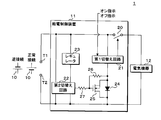
- FIG. 2 is a block diagram illustrating a main configuration of the power supply system according to the first embodiment.
- FIG. 4 is a circuit diagram of a second switching circuit. 6 is a timing chart for explaining an operation of the second switching circuit. It is explanatory drawing of the effect of a power supply control apparatus.
- FIG. 9 is a circuit diagram of a second switching circuit according to the second embodiment.
- FIG. 13 is a block diagram illustrating a main configuration of a power supply system according to a third embodiment.
- FIG. 15 is a block diagram illustrating a main configuration of a power supply system according to a fifth embodiment.
- an object of the present invention is to provide a circuit device in which an electric circuit is unlikely to stop operating suddenly.
- a circuit device is a circuit device including an electric circuit to which power is supplied when a DC voltage is applied between two terminals, and supplies power to the electric circuit.
- a diode disposed in a supply path, a switch connected between both ends of the diode, and, when the DC voltage is applied in a specific direction, the switch when the DC voltage is lower than a predetermined voltage.
- a switching circuit for switching from OFF to ON. When the DC voltage is applied in the specific direction and the switch is OFF, current flows in the order of the electric circuit and the diode.
- the switch is a transistor, and the switch has a first end disposed on the anode side of the diode in the supply path, and a switch in the supply path.
- a second terminal disposed on the cathode side of the diode, and a third terminal, wherein when a voltage of the third terminal increases, a resistance value between the first terminal and the second terminal decreases;
- the switching circuit switches the switch from off to on by increasing the voltage at the third terminal.
- the switch is an N-channel type FET (Field Effect Transistor) or an NPN type bipolar transistor.
- the switching circuit switches the switch from off to on by increasing the voltage at the third terminal corresponding to the gate or the base.
- the switch is an N-channel FET, and the diode is a parasitic diode of the switch.
- the switch is an N-channel type FET.
- a parasitic diode of a switch is used. Therefore, the manufacturing cost is low.
- the switching circuit includes a resistor having one end connected to the third end of the switch, and a second end having one end connected to the third end of the switch. And when the DC voltage is applied in the specific direction, a positive voltage is applied to the other end of the resistor based on the potential of the other end of the second switch, and the DC voltage Is applied in the specific direction, the second switch is switched from on to off when the DC voltage becomes lower than a predetermined voltage.
- the switch when the second switch is on, the switch is off because the voltage applied to the third terminal of the switch is low.
- the second switch is turned off. At this time, the voltage at the third terminal of the switch rises to a high voltage related to the DC voltage, and the switch is turned on.
- the switching circuit has a second switch having one end connected to the third end of the switch, and the DC voltage is applied in the specific direction.
- the DC voltage is When a positive voltage is applied to the other end of the second switch with reference to the potential of the cathode of the diode, and the DC voltage is applied in the specific direction, the DC voltage is When the voltage becomes lower than the voltage, the second switch switches from off to on.
- the switch when the second switch is off, the switch is off because the voltage applied to the third terminal of the switch is low.
- the second switch is turned on. At this time, the voltage at the third terminal of the switch rises to a high voltage related to the DC voltage, and the switch is turned on.
- the switching circuit includes a zener diode and a second resistor having one end connected to an anode of the zener diode, and the DC voltage is applied in the specific direction.
- a positive voltage is applied to the cathode of the Zener diode with reference to the potential at the other end of the second resistor, and the second switch responds to the voltage at one end of the second resistor. To switch on or off.
- the switch when the DC voltage is applied in a specific direction and the DC voltage is equal to or higher than a predetermined voltage, the current flows in the order of the Zener diode and the second resistor, and The voltage at one end is high. At this time, the switch is off. In the same case, when the DC voltage becomes lower than the predetermined voltage, the energization via the Zener diode stops, and the voltage at one end of the second resistor decreases. At this time, the second switch is turned on or off, and the switch is turned on.
- the circuit device includes a third switch, wherein the electric circuit switches the third switch on or off, and the DC voltage is applied to the two terminals. Then, electric power is supplied to the electric device via the third switch.
- the electric circuit controls power supply to the electric device by turning on or off the third switch.
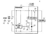
- FIG. 1 is a block diagram illustrating a main configuration of the power supply system 1 according to the first embodiment.
- the power supply system 1 is preferably mounted on a vehicle, and includes a battery 10, a power supply control device 11, an electric device 12, a positive terminal T1 and a negative terminal T2.
- the battery 10 is detachably connected between the positive terminal T1 and the negative terminal T2.
- the voltage of the positive electrode of the battery 10 based on the potential of the negative electrode of the battery 10 is referred to as a battery voltage.
- the battery voltage is a DC voltage.
- the connection of the battery 10 is a normal connection.
- the positive electrode and the negative electrode of the battery 10 are erroneously connected to the negative terminal T2 and the positive terminal T1, respectively, the connection of the battery 10 is a reverse connection.
- the battery 10 is connected to the positive terminal T1 and the negative terminal T2
- a battery voltage is applied between the positive terminal T1 and the negative terminal T2.
- the connection of the battery 10 is a normal connection, the battery voltage is applied in a specific direction.
- the connection of the battery 10 is a reverse connection, the battery voltage is applied in a direction different from the specific direction.
- the power supply control device 11 includes a power supply switch 20, a first switching circuit 21, a second switching circuit 22, a regulator 23, a diode 24, a bypass switch 25, and resistors 26 and 27.
- the bypass switch 25 is an N-channel FET and has a source, a drain, and a gate.
- the diode 24 is a parasitic diode of the bypass switch 25. Since the parasitic diode of the bypass switch 25 is used as the diode 24, the manufacturing cost of the power supply control device 11 is low.
- the positive terminal T1 is connected to one end of the power supply switch 20 of the power supply control device 11.
- the other end of the power supply switch 20 is connected to one end of the electric device 12.
- the other end of the electric device 12 is connected to the negative terminal T2.
- one end of the power supply switch 20 is further connected to a first switching circuit 21, a second switching circuit 22, and a regulator 23.
- the first switching circuit 21 is further connected to the anode of the diode 24.
- the cathode of the diode 24 is connected to the negative terminal T2.
- the source and the drain of the bypass switch 25 are connected to the anode and the cathode of the diode 24, respectively.
- a resistor 26 is connected between the gate and the source of the bypass switch 25.
- the gate of the bypass switch 25 is further connected to one end of the resistor 27.
- the other end of the resistor 27 is connected to the second switching circuit 22.
- the regulator 23 is further connected to the second switching circuit 22.
- the second switching circuit 22 is further connected to the negative terminal T2.
- the first switching circuit 21 operates when the applied voltage applied to the first switching circuit 21 is equal to or higher than the operating voltage required for operating the first switching circuit 21.
- the first switching circuit 21 receives an ON instruction for instructing the power supply switch 20 to be turned on and an OFF instruction for instructing the power supply switch 20 to be turned off.
- an ON instruction is input to the first switching circuit 21, the first switching circuit 21 switches the power supply switch 20 to ON.
- the power supply switch 20 is turned on when the connection of the battery 10 is normal, the battery 10 supplies power to the electric device 12 via the power supply switch 20. Thus, the electric device 12 operates.
- the first switching circuit 21 switches off the power supply switch 20 when an off instruction is input to the first switching circuit 21.
- the power supply switch 20 is turned off when the connection of the battery 10 is normal, the power supply from the battery 10 to the electric device 12 is stopped. Accordingly, the operation of the electric device 12 is stopped.
- the first switching circuit 21 controls the power supply from the battery 10 to the electric device 12 by turning on or off the power supply switch 20.
- Each of the power supply control device 11, the power supply switch 20, and the first switching circuit 21 functions as a circuit device, a third switch, and an electric circuit.
- the regulator 23 reduces the battery voltage to the voltage.
- the set voltage is a voltage based on the potential of the negative terminal T2.
- the battery voltage is, for example, 12V.
- the set voltage is, for example, 5V.
- the regulator 23 has a diode (not shown). The cathode of this diode is connected to the second switching circuit 22. In the regulator 23, the stepped-down voltage is output to the second switching circuit 22 via the diode. When the connection of the battery 10 is normal and the battery voltage is equal to or lower than the set voltage, the regulator 23 outputs the battery voltage to the second switching circuit 22 via the diode.
- the bypass switch 25 when the gate voltage based on the source potential is less than the first threshold value, the resistance between the drain and the source is large, and no current flows through the drain and the source. At this time, the bypass switch 25 is off.
- the first threshold is a constant voltage, which is above zero volts.
- a voltage drop occurs in the order of the anode and the cathode.
- the width of this voltage drop is referred to as a forward voltage.
- the forward voltage is, for example, 0.6V.
- the second switching circuit 22 sets the voltage of the gate of the bypass switch 25 based on the potential of the negative terminal T2 to substantially zero V To lower.
- the gate voltage based on the source potential is lower than the first threshold, and the bypass switch 25 switches from on to off.
- the reference voltage is constant.
- the path through which the current flows in the order of the positive terminal T1, the first switching circuit 21, the diode 24, and the negative terminal T2 is a supply path through which the battery 10 supplies power to the first switching circuit 21.
- a diode 24 is arranged in the supply path.
- the source of the bypass switch 25 is arranged on the anode side of the diode 24 in the supply path, and the drain of the bypass switch 25 is arranged on the cathode side of the diode 24.
- the source, drain and gate of the bypass switch 25 correspond to a first end, a second end and a third end.
- the voltage applied to the first switching circuit 21 is lower than the battery voltage. Specifically, the applied voltage substantially matches the voltage calculated by subtracting the forward voltage of the diode 24 from the battery voltage.
- the second switching circuit 22 changes the voltage of the gate of the bypass switch 25 with reference to the potential of the negative terminal T2 to the regulator 23. Is increased to a voltage close to the output voltage.
- the bypass switch 25 the gate voltage based on the source potential rises to a voltage equal to or higher than the first threshold, and the bypass switch 25 switches from off to on.
- the resistance of the bypass switch 25 is sufficiently small. For this reason, when the connection of the battery 10 is normal and the bypass switch 25 is on, the current flows in the order of the positive terminal T1, the first switching circuit 21, the bypass switch 25, and the negative terminal T2, Power is supplied to the switching circuit 21. At this time, since no voltage drop occurs in the diode 24, the applied voltage of the first switching circuit 21 substantially matches the battery voltage.
- the second switching circuit 22 When the connection of the battery 10 is reversed, the second switching circuit 22 does not output a voltage to the gate of the bypass switch 25. In this case, since no current flows through the resistors 26 and 27, the voltage of the gate of the bypass switch 25 based on the potential of the source is zero V, which is less than the first positive threshold. Therefore, when the connection of the battery 10 is a reverse connection, the bypass switch 25 is off.
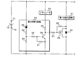
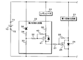
- FIG. 2 is a circuit diagram of the second switching circuit 22.
- the second switching circuit 22 has five resistors 30-34, a switching switch 35, and a zener diode 36.
- the changeover switch 35 is an NPN-type bipolar transistor.
- One end of the resistor 30 and the collector of the changeover switch 35 are connected to the other end of the resistor 27. As described above, one end of the resistor 27 is connected to the gate of the bypass switch 25. Therefore, one end of the resistor 30 and the collector of the changeover switch 35 are connected to the gate of the bypass switch 25 via the resistor 27.
- the changeover switch 35 functions as a second switch.
- the other end of the resistor 30 is connected to the regulator 23.
- the emitter of the changeover switch 35 is connected to the negative terminal T2.
- the resistor 31 is connected between the base and the emitter of the switch 35.
- the base of the changeover switch 35 is further connected to one end of the resistor 32.
- the other end of the resistor 32 is connected to one end of each of the resistors 33 and 34.
- the other end of the resistor 33 is connected to the negative terminal T2.
- the other end of the resistor 34 is connected to the anode of the Zener diode 36. Therefore, the anode of the Zener diode 36 is connected to one end of the resistor 33 via the resistor 34.
- the cathode of the Zener diode 36 is connected to the positive terminal T1.
- the regulator 23 reduces the battery voltage to the set voltage, and applies the reduced voltage to the other end of the resistor 30.
- the stepped-down voltage is a positive voltage based on the potential of the negative electrode terminal T2, that is, the potential of the emitter of the changeover switch 35.
- the second threshold is a constant voltage, which is above zero volts.
- the switch 35 is turned on or off in accordance with the voltage at one end of the resistor 33 with reference to the potential of the negative terminal T2.
- a current flows in the order of the resistors 32 and 31, and a voltage drop occurs in the resistor 31.
- the changeover switch 35 applies a positive voltage to the base with reference to the potential of the emitter. This positive voltage is higher as the width of the voltage drop generated in the resistor 31 is larger. The width of the voltage drop generated in the resistor 31 increases as the current flowing through the resistor 31 increases.
- the Zener diode 36 when the voltage of the cathode with respect to the potential of the anode becomes equal to or higher than a certain breakdown voltage, a current flows in the order of the cathode and the anode. In the Zener diode 36, when a current flows in the order of the cathode and the anode, the voltage across the Zener diode 36 is maintained at the breakdown voltage. In the Zener diode 36, when the voltage of the cathode based on the potential of the anode becomes lower than the breakdown voltage, the current supply through the cathode and the anode is stopped.
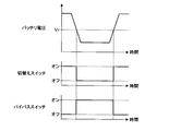
- FIG. 3 is a timing chart for explaining the operation of the second switching circuit 22.
- FIG. 3 shows the transition of the battery voltage and the transition of the changeover switch 35 and the bypass switch 25 on and off. Regarding these transitions, time is shown on the horizontal axis.
- FIG. 3 shows a transition of the battery voltage when the connection of the battery 10 is a normal connection. Vr indicates a reference voltage.
- a current is output via an internal resistor (not shown).
- an internal resistor not shown
- the width of the voltage drop increases as the current flowing through the internal resistance increases. The greater the magnitude of the voltage drop, the lower the battery voltage. Therefore, when the current output via the internal resistor fluctuates, the width of the voltage drop fluctuates, and the battery voltage fluctuates.
- the target to which the battery 10 supplies power includes a starter different from the electric device 12
- the starter when the starter operates, a large current flows through the internal resistance of the battery 10, and the battery voltage greatly decreases. I do.
- the starter is a motor for starting the engine. When the starter stops operating, the current flowing through the internal resistance of the battery 10 decreases, and the battery voltage greatly increases. Further, the battery voltage fluctuates according to the electric power stored in the battery 10.
- the battery voltage which is a positive voltage
- the cathode of the Zener diode 36 with reference to the negative terminal T2, that is, the potential of the other end of the resistor 33.
- the voltage of the cathode of the Zener diode 36 with respect to the potential of the anode is equal to or higher than the breakdown voltage.
- the current flows in the order of the Zener diode 36 and the resistors 34, 33, and also flows in the order of the Zener diode 36 and the resistors 34, 32, 31.
- the changeover switch 35 detects the base based on the potential of the emitter.
- the voltage is equal to or higher than the second threshold. In this case, the changeover switch 35 is on.
- the voltage of the gate of the bypass switch 25 based on the potential of the negative electrode terminal T2 is substantially zero volt.
- the gate voltage based on the source potential is less than the first positive threshold, and the bypass switch 25 is off.
- the changeover switch 35 and the bypass switch 25 are on and off, respectively, as shown in FIG. Since the bypass switch 25 is off, the current flows in the order of the first switching circuit 21 and the diode 24, and the applied voltage for the first switching circuit 21 is a voltage calculated by subtracting the forward voltage of the diode 24 from the battery voltage. Approximately matches.
- the changeover switch 35 is switched from on to off as shown in FIG. Switches from off to on.
- the bypass switch 25 is on, the current flows in the order of the first switching circuit 21 and the bypass switch 25, and the applied voltage of the first switching circuit 21 substantially matches the battery voltage.
- the changeover switch 35 is switched from off to on as shown in FIG. Switches from on to off.
- the current flows again in the order of the first switching circuit 21 and the diode 24, and the applied voltage of the first switching circuit 21 returns to the voltage calculated by subtracting the forward voltage of the diode 24 from the battery voltage.
- the connection of the battery 10 is a reverse connection
- the current flows in the order of the negative terminal T2, the resistors 33 and 34, the Zener diode 36 and the positive terminal T1, and the negative terminal T2, the resistors 31, 32 and 34, the Zener diode 36 and It flows in the order of the positive electrode terminal T1.
- the selector switch 35 the base voltage based on the potential of the emitter is a negative voltage, which is less than the positive second threshold.
- the changeover switch 35 is off.
- the regulator 23 When the connection of the battery 10 is reverse, the regulator 23 does not operate and no current flows through the resistor 26. Therefore, no voltage is output from the second switching circuit 22 to the gate of the bypass switch 25. At this time, as described above, the bypass switch 25 is off.
- the connection of the battery 10 is reverse connection, the current flows through the second switching circuit 22 as described above, but there is no problem.
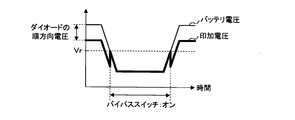
- FIG. 4 is an explanatory diagram of the effect of the power supply control device 11.
- the transition of the battery voltage is indicated by a thin solid line
- the transition of the applied voltage according to the first switching circuit 21 is indicated by a thick solid line.
- the transition of the portion where the battery voltage and the applied voltage are the same is indicated by a thick line.
- time is shown on the horizontal axis.
- FIG. 4 shows changes in the battery voltage and the applied voltage when the connection of the battery 10 is normal.
- the applied voltage according to the first switching circuit 21 substantially matches the voltage calculated by subtracting the forward voltage of the diode 24 from the battery voltage.
- the current flows through the first switching circuit 21 and the bypass switch 25 in this order because the bypass switch 25 is on.
- the applied voltage according to the first switching circuit 21 substantially matches the battery voltage.
- the bypass switch 25 is switched from off to on, and the applied voltage rises to the battery voltage. Therefore, there is a low possibility that the applied voltage becomes lower than the operating voltage necessary for the operation of the first switching circuit 21 and the operation of the first switching circuit 21 stops.
- the reference voltage Vr be equal to or higher than the voltage calculated by adding the forward voltage of the diode 24 to the minimum value of the battery voltage, as shown in FIG.
- the minimum value of the applied voltage is equal to or higher than the minimum value of the battery voltage, and does not become lower than the minimum value of the battery voltage.
- the diode 24 is disposed on the negative terminal T2 side of the first switching circuit 21, an inexpensive N-channel FET can be used as the bypass switch 25. Therefore, the manufacturing cost of the power supply control device 11 is low.
- the transistor used as the changeover switch 35 is not limited to an NPN-type bipolar transistor, and may be, for example, an N-channel type FET.
- the drain, source and gate of the FET respectively correspond to the collector, emitter and base of the bipolar transistor.
- FIG. 5 is a circuit diagram of the second switching circuit 22 according to the second embodiment.
- points of the second embodiment that are different from the first embodiment will be described.
- Other configurations except for the configuration described later are common to the first embodiment. Therefore, the same components as those in the first embodiment are denoted by the same reference numerals as those in the first embodiment, and description thereof will be omitted.
- the configuration of the second switching circuit 22 included in the power supply control device 11 is different.
- the second switching circuit 22 includes the resistors 30, 32-34 and the zener diode 36, as in the first embodiment.
- the second switching circuit 22 has a resistor 40 and a switch 41 instead of the resistor 31 and the switch 35.
- the changeover switch 41 is a P-channel type FET.
- the resistors 33 and 34 and the Zener diode 36 are connected in the same manner as in the first embodiment.
- One end of the resistor 30 is connected to the regulator 23.
- the other end of the resistor 30 is connected to the source of the changeover switch 41.
- the drain of the changeover switch 41 is connected to the other end of the resistor 27.
- one end of the resistor 27 is connected to the gate of the bypass switch 25. Therefore, the drain of the switch 41 is connected to the gate of the bypass switch 25 via the resistor 27.
- the changeover switch 41 functions as a second switch.
- the resistor 40 is connected between the gate and the source of the changeover switch 41.
- the gate of the changeover switch 41 is further connected to one end of the resistor 32.
- the other end of the resistor 32 is connected to one end of each of the resistors 33 and 34.
- the regulator 23 steps down the battery voltage to the set voltage and applies the stepped-down voltage to one end of the resistor 30.
- the stepped-down voltage is a positive voltage based on the potential of the negative electrode terminal T2, that is, the potential of the cathode of the diode 24.
- the changeover switch 41 when the voltage of the gate with respect to the potential of the source decreases, the resistance value between the source and the drain decreases. In the case of the changeover switch 41, when the gate voltage based on the source potential is equal to or less than the third threshold value, the resistance between the source and the drain is small, and current can flow through the source and the drain. At this time, the changeover switch 41 is on.
- the third threshold is a constant voltage, less than zero volts.
- the switch 41 is turned on or off in accordance with the voltage at one end of the resistor 33 with reference to the potential of the negative terminal T2.
- the voltage at one end of the resistor 33 with reference to the potential of the negative electrode terminal T2 is equal to or higher than the voltage output from the regulator 23, that is, the set voltage, no current flows through the resistors 30, 32, and 40.
- the changeover switch 41 the gate voltage based on the source potential is zero V, which exceeds the negative third threshold value. For this reason, the changeover switch 41 is off.
- the voltage at one end of the resistor 33 with reference to the potential of the negative electrode terminal T2 is lower than the set voltage, a current flows from the regulator 23 in the order of the resistors 30, 40, 32, and 33, and a voltage drop occurs at the resistor 40.
- the changeover switch 41 the gate voltage with respect to the source potential decreases.
- the width of the voltage drop generated in the resistor 40 is larger as the current flowing through the resistor 40 is larger.
- the gate voltage based on the source potential decreases as the width of the voltage drop generated by the resistor 40 increases.
- the changeover switch 41 when the connection of the battery 10 is normal and the voltage at one end of the resistor 33 with respect to the potential of the negative terminal T2 is high, the changeover switch 41 is off. In a similar case, when the voltage at one end of the resistor 33 with reference to the potential of the negative terminal T2 is low, the changeover switch 41 is on.
- a battery voltage that is a positive voltage is applied to the cathode of the Zener diode 36 based on the potential of the negative terminal T2.
- the voltage of the cathode of the Zener diode 36 with respect to the potential of the anode is equal to or higher than the breakdown voltage.
- the current flows in the order of the Zener diode 36 and the resistors 34 and 33, and the voltage at one end of the resistor 33 with respect to the potential of the negative terminal T2 is high. As a result, the changeover switch 41 is off.
- each of the switch 41 and the bypass switch 25 is switched from off to on.
- each of the changeover switch 41 and the bypass switch 25 is switched from on to off.
- the changeover switch 41 When the connection of the battery 10 is reverse connection, the current flows in the order of the negative terminal T2, the resistors 33 and 34, the Zener diode 36, and the positive terminal T1. Since the cathode of the regulator 23 is connected to one end of the resistor 30, no current flows through the resistors 30, 32, and 40. At this time, in the changeover switch 41, the gate voltage based on the source potential is zero V, which exceeds the negative third threshold value. Therefore, the changeover switch 41 is off. When the changeover switch 41 is off, the bypass switch 25 is off as described above.
- the bypass switch 25 switches from off to on. In the same case, when the battery voltage becomes equal to or higher than the reference voltage, the bypass switch 25 switches from on to off. When the connection of the battery 10 is reverse, the bypass switch 25 is off. Therefore, the power supply control device 11 according to the second embodiment has the same effects as the power supply control device 11 according to the first embodiment.
- the transistor used as the changeover switch 41 is not limited to a P-channel type FET, but may be, for example, a PNP type bipolar transistor.
- the emitter, collector and base of the bipolar transistor correspond to the source, drain and gate of the FET, respectively.
- FIG. 6 is a block diagram illustrating a main configuration of the power supply system 1 according to the third embodiment.
- points of the third embodiment that are different from the first embodiment will be described.
- Other configurations except for the configuration described later are common to the first embodiment. Therefore, the same components as those in the first embodiment are denoted by the same reference numerals as those in the first embodiment, and description thereof will be omitted.
- a difference between the first and third embodiments is whether the power supply control device 11 includes the regulator 23 or not.
- the power supply control device 11 according to the third embodiment has other components except the regulator 23 among the components included in the power supply control device 11 according to the first embodiment.
- the other end of the resistor 30 of the second switching circuit 22 is connected to one end of the power supply switch 20.
- the changeover switch 35 switches from ON to OFF as in the first embodiment.
- the changeover switch 35 is turned off, the gate voltage of the bypass switch 25 based on the potential of the negative terminal T2 rises to a voltage close to the battery voltage, and the bypass switch 25 is turned on.
- the changeover switch 35 switches from off to on and the bypass switch 25 switches from on to off, as in the first embodiment. Take the place.
- the changeover switch 35 and the bypass switch 25 are off as in the first embodiment.
- the power supply control device 11 according to the third embodiment has the same effects as the power supply control device 11 according to the first embodiment.
- the configuration of the second switching circuit 22 in the third embodiment is not limited to the configuration of the second switching circuit 22 in the first embodiment.
- points of the fourth embodiment that are different from the third embodiment will be described. Structures other than the structure described below are common to the third embodiment. Therefore, the same components as those of the third embodiment are denoted by the same reference numerals as those of the third embodiment, and description thereof will be omitted.
- the configuration of the second switching circuit 22 in the fourth embodiment is the same as the configuration of the second switching circuit 22 (see FIG. 5) in the second embodiment.
- one end of the resistor 30 of the second switching circuit 22 is connected to one end of the power supply switch 20.
- the switch 41 switches from off to on.
- the changeover switch 41 is turned on, the voltage of the gate of the bypass switch 25 based on the potential of the negative terminal T2 rises to a voltage close to the battery voltage, and the bypass switch 25 is turned on.
- the changeover switch 41 When the connection of the battery 10 is reverse connection, the current flows in the order of the negative terminal T2, the resistors 33 and 34, the Zener diode 36 and the positive terminal T1, and the negative terminal T2, the resistors 33, 32, 40 and 30 and the positive terminal. It flows in the order of T1.
- the changeover switch 41 the gate voltage based on the source potential is a positive voltage and is equal to or more than the negative third threshold. Therefore, the changeover switch 41 is off.
- the bypass switch 25 is off as in the second embodiment.
- the power supply control device 11 according to the fourth embodiment has the same effects as the power supply control device 11 according to the second embodiment.
- FIG. 7 is a block diagram illustrating a main configuration of the power supply system 1 according to the fifth embodiment.
- points of the fifth embodiment that are different from the first embodiment will be described.
- Other configurations except for the configuration described later are common to the first embodiment. Therefore, the same components as those in the first embodiment are denoted by the same reference numerals as those in the first embodiment, and description thereof will be omitted.
- the power supply control device 11 according to the fifth embodiment has other components except the bypass switch 25 and the resistor 26 among the components included in the power supply control device 11 according to the first embodiment.
- the power supply control device 11 according to the fifth embodiment includes a bypass switch 50 and a resistor 51 instead of the bypass switch 25 and the resistor 26.
- the bypass switch 50 is an NPN-type bipolar transistor. When a bipolar transistor is manufactured, no parasitic diode is generated. For this reason, the diode 24 in the third embodiment is a normal element.
- the collector and the emitter of the bypass switch 50 are connected to the anode and the cathode of the diode 24, respectively.
- a resistor 51 is connected between the base and the emitter of the bypass switch 50.
- the base of the bypass switch 50 is further connected to one end of the resistor 27.
- bypass switch 50 when the base voltage with respect to the emitter potential increases, the resistance value between the collector and the emitter decreases.
- the voltage of the base of the bypass switch 50 with respect to the potential of the emitter is equal to or higher than the fourth threshold value, the resistance between the collector and the emitter is small, and the current can flow through the collector and the emitter. At this time, the bypass switch 50 is on.
- the fourth threshold is a constant voltage, which is above zero volts.
- the changeover switch 35 switches from ON to OFF as in the first embodiment.
- the changeover switch 35 is turned off, in the bypass switch 50, the voltage of the base of the bypass switch 50 based on the potential of the emitter rises to a voltage close to the output voltage of the regulator 23 and becomes equal to or higher than the fourth threshold value. .
- the bypass switch 50 switches from off to on.
- the changeover switch 35 switches from off to on and the bypass switch 50 switches from on to off as in the first embodiment. Take the place.
- the changeover switch 35 is off as in the first embodiment.
- the diode of the regulator 23 is connected to the other end of the resistor 30, when the connection of the battery 10 is reversed, no current flows through the resistor 51, and the bypass switch 50 is also off.
- the on / off switching of the changeover switch 35 and the bypass switch 50 is performed in the same manner as the on / off switching of the changeover switch 35 and the bypass switch 25 in the first embodiment. Therefore, the power supply control device 11 according to the fifth embodiment has the same effects as the power supply control device 11 according to the first embodiment.
- the regulator 23 may be omitted as in the third embodiment.
- switching on and off of the changeover switch 35 and the bypass switch 50 is performed in the same manner as switching on and off of the changeover switch 35 and the bypass switch 25 in the third embodiment.
- a current flows in the order of the negative terminal T2, the resistors 51, 27, 30 and the positive terminal T1.
- the bypass switch 50 the base voltage based on the potential of the emitter is a negative voltage, which is less than the positive fourth threshold. As a result, the bypass switch 50 is off.
- the configuration of the second switching circuit 22 in the fifth embodiment is not limited to the configuration of the second switching circuit 22 in the first embodiment.
- points of the sixth embodiment that are different from the fifth embodiment will be described. Structures other than the structure described below are common to the fifth embodiment. Therefore, the same components as those in the fifth embodiment are denoted by the same reference numerals as those in the fifth embodiment, and description thereof will be omitted.
- the configuration of the second switching circuit 22 in the sixth embodiment is the same as the configuration of the second switching circuit 22 (see FIG. 5) in the second embodiment.
- the changeover switch 41 switches from off to on as in the second embodiment.
- the changeover switch 41 is turned on, in the bypass switch 50, the voltage of the base of the bypass switch 50 based on the potential of the emitter rises to a voltage close to the output voltage of the regulator 23 and becomes equal to or higher than the fourth threshold value. .
- the bypass switch 50 switches from off to on.
- the changeover switch 41 switches from on to off and the bypass switch 50 switches from on to off, as in the second embodiment. Take the place.
- the changeover switch 41 is off as in the second embodiment.
- the diode of the regulator 23 is connected to one end of the resistor 30, when the connection of the battery 10 is reversed, no current flows through the resistor 51, and the bypass switch 50 is also off.
- the on / off switching of the changeover switch 41 and the bypass switch 50 is performed in the same manner as the on / off switching of the changeover switch 41 and the bypass switch 25 in the second embodiment. Therefore, the power supply control device 11 according to the sixth embodiment has the same effects as the power supply control device 11 according to the second embodiment.
- the regulator 23 may be omitted as in the fourth embodiment.
- the on / off switching of the changeover switch 41 and the bypass switch 50 is performed in the same manner as the on / off switching of the changeover switch 41 and the bypass switch 25 in the fourth embodiment.
- a current flows in the order of the negative terminal T2, the resistors 51, 27, 30 and the positive terminal T1.
- the bypass switch 50 the base voltage based on the potential of the emitter is a negative voltage, which is less than the positive fourth threshold. As a result, the bypass switch 50 is off.
- the electric circuit arranged on the upstream side of the diode 24 in the supply path for supplying power from the battery 10 is not limited to the first switching circuit 21.
- the electric circuit arranged on the upstream side of the diode 24 may be any circuit that operates when power is supplied from the battery 10.
Landscapes
- Engineering & Computer Science (AREA)
- Physics & Mathematics (AREA)
- Power Engineering (AREA)
- General Physics & Mathematics (AREA)
- Nonlinear Science (AREA)
- Electromagnetism (AREA)
- Radar, Positioning & Navigation (AREA)
- Automation & Control Theory (AREA)
- Microelectronics & Electronic Packaging (AREA)
- Business, Economics & Management (AREA)
- Emergency Management (AREA)
- Charge And Discharge Circuits For Batteries Or The Like (AREA)
- Direct Current Feeding And Distribution (AREA)
Abstract
給電制御装置(11)では、バッテリ(10)の接続が正常接続である場合において、バイパススイッチ(25)がオフであるとき、電流は第1切替え回路(21)及びダイオード(24)の順に流れる。バッテリ(10)の接続が正常接続である場合において、バッテリ(10)の出力電圧が基準電圧未満となったとき、第2切替え回路(22)はバイパススイッチ(25)をオフからオンに切替える。
Description
本開示は回路装置に関する。
本出願は、2018年7月25日出願の日本出願第2018-139769号に基づく優先権を主張し、前記日本出願に記載された全ての記載内容を援用するものである。
本出願は、2018年7月25日出願の日本出願第2018-139769号に基づく優先権を主張し、前記日本出願に記載された全ての記載内容を援用するものである。
特許文献1には、電気回路を備える車両用の回路装置が開示されている。この回路装置では、電気回路にダイオードのカソードが接続されている。ダイオードのアノードにバッテリの正極が接続された場合、ダイオードを介してバッテリから電気回路に電力が供給され、電気回路は作動する。
バッテリの負極を誤ってダイオードのアノードに接続した場合、ダイオードの作用により、バッテリから電気回路に電流が流れることはない。このため、極性が誤っている電圧が電気回路に印加されることはない。
本開示の一態様に係る回路装置は、2つの端子間に直流電圧が印加された場合に電力が供給される電気回路を備える回路装置であって、前記電気回路に電力を供給する供給経路に配置されるダイオードと、前記ダイオードの両端間に接続されるスイッチと、前記直流電圧が特定方向に印加されている場合にて、前記直流電圧が所定電圧未満となったときに前記スイッチをオフからオンに切替える切替え回路とを備え、前記直流電圧が前記特定方向に印加された場合にて、前記スイッチがオフであるとき、電流は前記電気回路及びダイオードの順に流れる。
[本開示が解決しようとする課題]
ダイオードに電流が流れた場合、ダイオードでは電圧降下が発生する。このため、ダイオードを介してバッテリから電気回路に電力が供給されている場合、電気回路に印加される電圧は、バッテリの出力電圧よりも低い。通常、車両に搭載されるバッテリの出力電圧は、一定ではなく、変動する。バッテリの出力電圧が低下した場合、電気回路に印加される電圧も低下する。
ダイオードに電流が流れた場合、ダイオードでは電圧降下が発生する。このため、ダイオードを介してバッテリから電気回路に電力が供給されている場合、電気回路に印加される電圧は、バッテリの出力電圧よりも低い。通常、車両に搭載されるバッテリの出力電圧は、一定ではなく、変動する。バッテリの出力電圧が低下した場合、電気回路に印加される電圧も低下する。
特許文献1に記載の回路装置では、バッテリの出力電圧が低下した場合において、電気回路に印加される電圧が、電気回路の作動に必要な作動電圧未満となる可能性が高い。電気回路に印加される電圧が作動電圧未満となった場合、電気回路は突然に動作を停止する。
そこで、電気回路が突然に動作を停止する可能性が低い回路装置を提供することを目的とする。
[本開示の効果]
本開示によれば、電気回路が突然に動作を停止する可能性が低い。
本開示によれば、電気回路が突然に動作を停止する可能性が低い。
[本開示の実施形態の説明]
最初に本開示の実施態様を列挙して説明する。以下に記載する実施形態の少なくとも一部を任意に組み合わせてもよい。
最初に本開示の実施態様を列挙して説明する。以下に記載する実施形態の少なくとも一部を任意に組み合わせてもよい。
(1)本開示の一態様に係る回路装置は、2つの端子間に直流電圧が印加された場合に電力が供給される電気回路を備える回路装置であって、前記電気回路に電力を供給する供給経路に配置されるダイオードと、前記ダイオードの両端間に接続されるスイッチと、前記直流電圧が特定方向に印加されている場合にて、前記直流電圧が所定電圧未満となったときに前記スイッチをオフからオンに切替える切替え回路とを備え、前記直流電圧が前記特定方向に印加された場合にて、前記スイッチがオフであるとき、電流は前記電気回路及びダイオードの順に流れる。
上記の一態様にあっては、直流電圧が特定方向とは異なる方向に印加されている場合において、スイッチがオフであるとき、ダイオードの作用により、電気回路に電流が流れない。従って、極性が誤った電圧が電気回路に印加されることを防止することができる。直流電圧が特定方向に印加されている場合において、スイッチがオフであるとき、電流は電気回路及びダイオードの順に流れ、ダイオードで電圧降下が発生する。同様の場合において、スイッチがオンであるとき、電流が電気回路及びスイッチの順に流れ、ダイオードで電圧降下が発生しない。
直流電圧が特定方向に印加されている場合において、直流電圧が所定電圧未満となったとき、スイッチがオフからオンに切替わり、電気回路に印加される電圧が上昇する。このため、電気回路に印加される電圧が、電気回路の作動に必要な作動電圧未満となって電気回路の動作が停止する可能性は低い。
(2)本開示の一態様に係る回路装置では、前記スイッチは、トランジスタであり、前記スイッチは、前記供給経路にて前記ダイオードのアノード側に配置される第1端と、前記供給経路にて前記ダイオードのカソード側に配置される第2端と、第3端とを有し、前記第3端の電圧が上昇した場合に前記第1端及び第2端間の抵抗値が低下し、前記切替え回路は、前記第3端の電圧を上昇させることによって、前記スイッチをオフからオンに切替える。
上記の一態様にあっては、スイッチは、Nチャネル型のFET(Field Effect Transistor)、又は、NPN型のバイポーラトランジスタ等である。切替え回路は、ゲート又はベース等に相当する第3端の電圧を上昇させることによって、スイッチをオフからオンに切替える。
(3)本開示の一態様に係る回路装置では、前記スイッチは、Nチャネル型のFETであり、前記ダイオードは、前記スイッチの寄生ダイオードである。
上記の一態様にあっては、スイッチはNチャネル型のFETである。供給経路に配置されるダイオードとして、スイッチの寄生ダイオードを用いる。このため、製造費用が安価である。
(4)本開示の一態様に係る回路装置では、前記切替え回路は、一端が前記スイッチの前記第3端に接続される抵抗と、一端が前記スイッチの前記第3端に接続される第2のスイッチとを有し、前記直流電圧が前記特定方向に印加された場合に、前記第2のスイッチの他端の電位を基準として前記抵抗の他端に正の電圧が印加され、前記直流電圧が前記特定方向に印加されている場合にて、前記直流電圧が所定電圧未満となったときに前記第2のスイッチはオンからオフに切替わる。
上記の一態様にあっては、第2のスイッチがオンである場合、スイッチの第3端に印加される電圧は低いので、スイッチはオフである。直流電圧が特定方向に印加されている場合において、直流電圧が所定電圧未満となったとき、第2のスイッチはオフに切替わる。このとき、スイッチの第3端の電圧が直流電圧に係る高い電圧に上昇し、スイッチがオンに切替わる。
(5)本開示の一態様に係る回路装置では、前記切替え回路は、一端が前記スイッチの前記第3端に接続される第2のスイッチを有し、前記直流電圧が前記特定方向に印加された場合に、前記ダイオードのカソードの電位を基準として前記第2のスイッチの他端に正の電圧が印加され、前記直流電圧が前記特定方向に印加されている場合にて、前記直流電圧が所定電圧未満となったときに前記第2のスイッチはオフからオンに切替わる。
上記の一態様にあっては、第2のスイッチがオフである場合、スイッチの第3端に印加される電圧は低いので、スイッチはオフである。直流電圧が特定方向に印加されている場合において、直流電圧が所定電圧未満となったとき、第2のスイッチはオンに切替わる。このとき、スイッチの第3端の電圧が直流電圧に係る高い電圧に上昇し、スイッチがオンに切替わる。
(6)本開示の一態様に係る回路装置では、前記切替え回路は、ツェナーダイオードと、前記ツェナーダイオードのアノードに一端が接続される第2の抵抗とを備え、前記直流電圧が前記特定方向に印加された場合に、前記第2の抵抗の他端の電位を基準として前記ツェナーダイオードのカソードに正の電圧が印加され、前記第2のスイッチは、前記第2の抵抗の一端の電圧に応じてオン又はオフに切替わる。
上記の一態様にあっては、直流電圧が特定方向に印加されている場合において、直流電圧が所定電圧以上であるとき、電流がツェナーダイオード及び第2の抵抗の順に流れ、第2の抵抗の一端の電圧は高い。このとき、スイッチはオフである。同様の場合において、直流電圧が所定電圧未満となったとき、ツェナーダイオードを介した通電が停止し、第2の抵抗の一端の電圧が低下する。このとき、第2のスイッチはオン又はオフに切替わり、スイッチがオンに切替わる。
(7)本開示の一態様に係る回路装置は、第3のスイッチを備え、前記電気回路は前記第3のスイッチをオン又はオフに切替え、前記2つの端子に前記直流電圧が印加された場合に、前記第3のスイッチを介して電気機器に電力が供給される。
上記の一態様にあっては、電気回路は第3のスイッチをオン又はオフに切替えることによって、電気機器への給電を制御する。
[本開示の実施形態の詳細]
本開示の実施形態に係る電源システムの具体例を、以下に図面を参照しつつ説明する。なお、本発明はこれらの例示に限定されるものではなく、請求の範囲によって示され、請求の範囲と均等の意味および範囲内でのすべての変更が含まれることが意図される。
本開示の実施形態に係る電源システムの具体例を、以下に図面を参照しつつ説明する。なお、本発明はこれらの例示に限定されるものではなく、請求の範囲によって示され、請求の範囲と均等の意味および範囲内でのすべての変更が含まれることが意図される。
(実施形態1)
図1は、実施形態1における電源システム1の要部構成を示すブロック図である。電源システム1は、好適に車両に搭載されており、バッテリ10、給電制御装置11、電気機器12、正極端子T1及び負極端子T2を備える。バッテリ10は、正極端子T1及び負極端子T2間に着脱可能に接続される。以下では、バッテリ10の負極の電位を基準としたバッテリ10の正極の電圧をバッテリ電圧と記載する。バッテリ電圧は直流電圧である。
図1は、実施形態1における電源システム1の要部構成を示すブロック図である。電源システム1は、好適に車両に搭載されており、バッテリ10、給電制御装置11、電気機器12、正極端子T1及び負極端子T2を備える。バッテリ10は、正極端子T1及び負極端子T2間に着脱可能に接続される。以下では、バッテリ10の負極の電位を基準としたバッテリ10の正極の電圧をバッテリ電圧と記載する。バッテリ電圧は直流電圧である。
バッテリ10の正極及び負極夫々が正極端子T1及び負極端子T2に接続されている場合、バッテリ10の接続は正常接続である。バッテリ10の正極及び負極夫々が負極端子T2及び正極端子T1に誤って接続されている場合、バッテリ10の接続は逆接続である。バッテリ10が正極端子T1及び負極端子T2に接続された場合、バッテリ電圧が正極端子T1及び負極端子T2間に印加される。バッテリ10の接続が正常接続である場合、バッテリ電圧は特定方向に印加される。バッテリ10の接続が逆接続である場合、バッテリ電圧は特定方向とは異なる方向に印加される。
給電制御装置11は、給電スイッチ20、第1切替え回路21、第2切替え回路22、レギュレータ23、ダイオード24、バイパススイッチ25及び抵抗26,27を有する。バイパススイッチ25は、Nチャネル型のFETであり、ソース、ドレイン及びゲートを有する。ダイオード24は、バイパススイッチ25の寄生ダイオードである。ダイオード24として、バイパススイッチ25の寄生ダイオードを用いるので、給電制御装置11の製造費用は安価である。
電源システム1では、正極端子T1は、給電制御装置11の給電スイッチ20の一端に接続されている。給電スイッチ20の他端は、電気機器12の一端に接続されている。電気機器12の他端は負極端子T2に接続されている。
給電制御装置11内では、給電スイッチ20の一端は、更に、第1切替え回路21、第2切替え回路22及びレギュレータ23に接続されている。第1切替え回路21は、更に、ダイオード24のアノードに接続されている。ダイオード24のカソードは、負極端子T2に接続されている。バイパススイッチ25のソース及びドレイン夫々は、ダイオード24のアノード及びカソードに接続されている。バイパススイッチ25のゲート及びソース間に抵抗26が接続されている。バイパススイッチ25のゲートは、更に、抵抗27の一端に接続されている。抵抗27の他端は第2切替え回路22に接続されている。レギュレータ23は、更に、第2切替え回路22に接続されている。第2切替え回路22は、更に、負極端子T2に接続されている。
バッテリ10の接続が正常接続である場合、電流がバッテリ10の正極から第1切替え回路21に流れ、バッテリ10は第1切替え回路21に電圧を印加する。これにより、第1切替え回路21に電力が供給される。第1切替え回路21は、第1切替え回路21に印加されている印加電圧が、第1切替え回路21の作動に必要な作動電圧以上である場合に作動する。
第1切替え回路21には、給電スイッチ20のオンを指示するオン指示と、給電スイッチ20のオフを指示するオフ指示とが入力される。第1切替え回路21は、第1切替え回路21にオン指示が入力された場合、給電スイッチ20をオンに切替える。バッテリ10の接続が正常接続である場合において、給電スイッチ20がオンに切替わったとき、バッテリ10は、給電スイッチ20を介して電気機器12に電力を供給する。これにより、電気機器12は作動する。
第1切替え回路21は、第1切替え回路21にオフ指示が入力された場合、給電スイッチ20をオフに切替える。バッテリ10の接続が正常接続である場合において、給電スイッチ20がオフに切替わったとき、バッテリ10から電気機器12への給電が停止する。これにより、電気機器12は動作を停止する。
給電制御装置11では、第1切替え回路21が給電スイッチ20をオン又はオフに切替えることによって、バッテリ10から電気機器12への給電を制御する。
給電制御装置11、給電スイッチ20及び第1切替え回路21夫々は、回路装置、第3のスイッチ及び電気回路として機能する。
給電制御装置11、給電スイッチ20及び第1切替え回路21夫々は、回路装置、第3のスイッチ及び電気回路として機能する。
第1切替え回路21に係る印加電圧が作動電圧未満となるか、又は、バッテリ10から第1切替え回路21への給電が停止した場合、第1切替え回路21は動作を停止する。第1切替え回路21が動作を停止している場合、給電スイッチ20はオフであり、電気機器12に電力が供給されることはない。
バッテリ10の接続が正常接続である場合において、バッテリ電圧が、予め設定されている設定電圧を超えているとき、レギュレータ23は、バッテリ電圧を設定電圧に降圧する。設定電圧は、負極端子T2の電位を基準とした電圧である。バッテリ電圧は例えば12Vである。設定電圧は例えば5Vである。
レギュレータ23は図示しないダイオードを有する。このダイオードのカソードは第2切替え回路22に接続されている。レギュレータ23では、降圧した電圧はダイオードを介して第2切替え回路22に出力する。バッテリ10の接続が正常接続である場合において、バッテリ電圧が設定電圧以下であるとき、レギュレータ23では、ダイオードを介してバッテリ電圧を第2切替え回路22に出力する。
前述したように、レギュレータ23のダイオードのカソードは第2切替え回路22に接続されているので、電流が第2切替え回路22及びレギュレータ23の順に流れることはない。
バイパススイッチ25について、ソースの電位を基準としたゲートの電圧が上昇した場合、ドレイン及びソース間の抵抗値が低下する。バイパススイッチ25について、ソースの電位を基準としたゲートの電圧が第1閾値以上である場合、ドレイン及びソース間の抵抗値が小さく、ドレイン及びソースを介して電流が流れることが可能である。このとき、バイパススイッチ25はオンである。
また、バイパススイッチ25について、ソースの電位を基準としたゲートの電圧が第1閾値未満である場合、ドレイン及びソース間の抵抗値が大きく、ドレイン及びソースを介して電流が流れることはない。このとき、バイパススイッチ25はオフである。第1閾値は、一定の電圧であり、ゼロVを超えている。
ダイオード24において、電流がアノード及びカソードの順に流れた場合、電圧降下が発生する。以下では、この電圧降下の幅を順方向電圧と記載する。順方向電圧は、例えば0.6Vである。
バッテリ10の接続が正常接続である場合において、バッテリ電圧が基準電圧以上となったとき、第2切替え回路22は、負極端子T2の電位を基準としたバイパススイッチ25のゲートの電圧を略ゼロVに低下させる。このとき、バイパススイッチ25において、ソースの電位を基準としたゲートの電圧は第1閾値未満となり、バイパススイッチ25はオンからオフに切替わる。基準電圧は一定である。
バッテリ10の接続が正常接続である場合において、バイパススイッチ25がオフであるとき、電流は、正極端子T1、第1切替え回路21、ダイオード24及び負極端子T2の順に流れ、第1切替え回路21に電力が供給される。
電流は、正極端子T1、第1切替え回路21、ダイオード24及び負極端子T2の順に流れる経路は、バッテリ10が第1切替え回路21に電力を供給する供給経路である。供給経路にダイオード24が配置されている。供給経路において、バイパススイッチ25のソースは、供給経路においてダイオード24のアノード側に配置され、バイパススイッチ25のドレインは、ダイオード24のカソード側に配置されている。バイパススイッチ25のソース、ドレイン及びゲートは、第1端、第2端及び第3端に相当する。
電流は、正極端子T1、第1切替え回路21、ダイオード24及び負極端子T2の順に流れている場合、ダイオード24では電圧降下が発生する。この場合、第1切替え回路21に係る印加電圧は、バッテリ電圧よりも低い。具体的には、印加電圧は、バッテリ電圧からダイオード24の順方向電圧を減算することによって算出される電圧に略一致する。
バッテリ10の接続が正常接続である場合において、バッテリ電圧が基準電圧未満となったとき、第2切替え回路22は、負極端子T2の電位を基準としたバイパススイッチ25のゲートの電圧を、レギュレータ23の出力電圧に近い電圧に上昇させる。これにより、バイパススイッチ25では、ソースの電位を基準としたゲートの電圧は、第1閾値以上である電圧に上昇し、バイパススイッチ25はオフからオンに切替わる。
バイパススイッチ25がオンである場合、バイパススイッチ25の抵抗値は十分に小さい。このため、バッテリ10の接続が正常接続である場合において、バイパススイッチ25がオンであるとき、電流は、正極端子T1、第1切替え回路21、バイパススイッチ25及び負極端子T2の順に流れ、第1切替え回路21に電力が供給される。このとき、ダイオード24で電圧降下が発生しないので、第1切替え回路21係る印加電圧は、バッテリ電圧に略一致する。
バッテリ10の接続が逆接続である場合、第2切替え回路22はバイパススイッチ25のゲートに電圧を出力することはない。この場合、抵抗26,27に電流が流れないので、バイパススイッチ25において、ソースの電位を基準としたゲートの電圧は、ゼロVであり、正の第1閾値未満である。従って、バッテリ10の接続が逆接続である場合、バイパススイッチ25はオフである。
バッテリ10の接続が逆接続である場合、ダイオード24及びバイパススイッチ25のいずれも電流は流れることはない。このため、バッテリ10の接続が逆接続である場合、電流は第1切替え回路21を流れることはなく、極性が誤った電圧が第1切替え回路21に印加されることを防止することができる。
バッテリ10の接続が逆接続である場合、電流は第1切替え回路21を流れることはないので、第1切替え回路21に電力が供給されることはない。前述したように、第1切替え回路21に電力が供給されていない場合、給電スイッチ20はオフである。このため、バッテリ10の接続が逆接続である場合、電気機器12に電流が流れず、電気機器12に電力が供給されることはない。電気機器12に電力が供給されていない場合、電気機器12は動作を停止している。
図2は第2切替え回路22の回路図である。第2切替え回路22は、5つの抵抗30-34、切替えスイッチ35及びツェナーダイオード36を有する。切替えスイッチ35は、NPN型のバイポーラトランジスタである。
抵抗30の一端及び切替えスイッチ35のコレクタ夫々は、抵抗27の他端に接続されている。前述したように、抵抗27の一端はバイパススイッチ25のゲートに接続されている。従って、抵抗30の一端及び切替えスイッチ35のコレクタ夫々は、抵抗27を介してバイパススイッチ25のゲートに接続されている。切替えスイッチ35は第2のスイッチとして機能する。
抵抗30の他端はレギュレータ23に接続されている。切替えスイッチ35のエミッタは負極端子T2に接続されている。切替えスイッチ35のベース及びエミッタ間に抵抗31が接続されている。切替えスイッチ35のベースは、更に、抵抗32の一端に接続されている。抵抗32の他端は、抵抗33,34夫々の一端が接続されている。抵抗33の他端は負極端子T2に接続されている。抵抗34の他端は、ツェナーダイオード36のアノードに接続されている。従って、ツェナーダイオード36のアノードは抵抗34を介して抵抗33の一端に接続されている。ツェナーダイオード36のカソードは正極端子T1に接続されている。
バッテリ10の接続が正常接続である場合、レギュレータ23はバッテリ電圧を設定電圧に降圧し、降圧した電圧を抵抗30の他端に印加する。降圧した電圧は、負極端子T2の電位、即ち、切替えスイッチ35のエミッタの電位を基準とした正の電圧である。
切替えスイッチ35について、エミッタの電位を基準としたベースの電圧が上昇した場合、コレクタ及びエミッタ間の抵抗値が低下する。切替えスイッチ35について、エミッタの電位を基準としたベースの電圧が第2閾値以上である場合、コレクタ及びエミッタ間の抵抗値が小さく、コレクタ及びエミッタを介して電流が流れることが可能である。このとき、切替えスイッチ35はオンである。
また、切替えスイッチ35について、エミッタの電位を基準としたベースの電圧が第2閾値未満である場合、コレクタ及びエミッタ間の抵抗値は大きく、コレクタ及びエミッタを介して電流が流れることはない。このとき、切替えスイッチ35はオフである。第2閾値は、一定の電圧であり、ゼロVを超えている。
切替えスイッチ35は、負極端子T2の電位を基準とした抵抗33の一端の電圧に応じて、オン又はオフに切替わる。抵抗33の一端の電圧がゼロVを超えている場合、電流が抵抗32,31の順に流れ、抵抗31で電圧降下が発生する。このとき、切替えスイッチ35では、エミッタの電位を基準としてベースに正の電圧が印加される。この正の電圧は、抵抗31で発生する電圧降下の幅が大きい程、高い。抵抗31で発生する電圧降下の幅は、抵抗31を流れる電流が大きい程、大きい。
負極端子T2の電位を基準とした抵抗33の一端の電圧が高い程、抵抗31を流れる電流が大きく、エミッタの電位を基準としたベースの電圧が高い。前述したように、切替えスイッチ35は、エミッタの電位を基準としたベースの電圧に応じてオン又はオフに切替わる。
ツェナーダイオード36では、アノードの電位を基準としたカソードの電圧が一定の降伏電圧以上となった場合、電流がカソード及びアノードの順に流れる。ツェナーダイオード36において、電流がカソード及びアノードの順に流れている場合、ツェナーダイオード36の両端間の電圧は降伏電圧に維持される。ツェナーダイオード36において、アノードの電位を基準としたカソードの電圧が降伏電圧未満となった場合、カソード及びアノードを介した通電が停止する。
図3は、第2切替え回路22の動作を説明するためのタイミングチャートである。図3では、バッテリ電圧の推移と、切替えスイッチ35及びバイパススイッチ25夫々のオン及びオフに係る推移とが示されている。これらの推移について、横軸には、時間が示されている。図3には、バッテリ10の接続は正常接続である場合におけるバッテリ電圧の推移が示されている。Vrは基準電圧を示す。
バッテリ電圧は、種々の理由で変動する。バッテリ10では、図示しない内部抵抗を介して電流が出力される。内部抵抗を電流が流れた場合、内部抵抗で電圧降下が発生する。電圧降下の幅は、内部抵抗を流れる電流が大きい程、大きい。電圧降下の幅が大きい程、バッテリ電圧は低い。従って、内部抵抗を介して出力される電流が変動した場合、電圧降下の幅が変動し、バッテリ電圧が変動する。
例えば、バッテリ10が電力を供給する対象に、電気機器12とは異なるスタータが含まれている場合においては、スタータが作動したとき、バッテリ10の内部抵抗を大きな電流が流れ、バッテリ電圧が大きく低下する。スタータはエンジンを始動させるためのモータである。スタータが動作を停止したとき、バッテリ10の内部抵抗を流れる電流が低下し、バッテリ電圧が大きく上昇する。
また、バッテリ電圧は、バッテリ10に蓄えられている電力にも応じて変動する。
また、バッテリ電圧は、バッテリ10に蓄えられている電力にも応じて変動する。
図2に示すように、バッテリ10の接続が正常接続である場合、負極端子T2、即ち、抵抗33の他端の電位を基準として、ツェナーダイオード36のカソードに、正の電圧であるバッテリ電圧が印加される。バッテリ10の接続が正常接続である場合において、バッテリ電圧が基準電圧Vr以上であるとき、ツェナーダイオード36では、アノードの電位を基準としたカソードの電圧は降伏電圧以上である。このとき、電流は、ツェナーダイオード36及び抵抗34,33の順に流れるとともに、ツェナーダイオード36及び抵抗34,32,31の順に流れる。
電流がツェナーダイオード36のカソード及びアノードの順に流れている場合、負極端子T2の電位を基準とした抵抗31の一端の電圧は十分に高く、切替えスイッチ35では、エミッタの電位を基準としたベースの電圧は第2閾値以上である。この場合、切替えスイッチ35はオンである。
切替えスイッチ35がオンである場合、負極端子T2の電位を基準としたバイパススイッチ25のゲートの電圧は、略ゼロVである。このとき、バイパススイッチ25では、ソースの電位を基準としたゲートの電圧は、正の第1閾値未満であり、バイパススイッチ25はオフである。
以上のように、バッテリ10の接続が正常接続である場合において、バッテリ電圧が基準電圧Vr以上であるとき、図3に示すように、切替えスイッチ35及びバイパススイッチ25夫々はオン及びオフである。バイパススイッチ25はオフであるので、電流は第1切替え回路21及びダイオード24の順に流れ、第1切替え回路21係る印加電圧はバッテリ電圧からダイオード24の順方向電圧を減算することによって算出される電圧に略一致する。
バッテリ電圧が基準電圧Vr未満となった場合、ツェナーダイオード36では、アノードの電位を基準としたカソードの電圧は降伏電圧未満となり、ツェナーダイオード36を介した通電が停止する。このとき、電流が抵抗33を流れることはないため、負極端子T2の電位を基準とした抵抗33の一端の電圧はゼロVに低下する。このとき、抵抗31にも電流が流れないため、切替えスイッチ35では、エミッタの電位を基準としたベースの電圧は、ゼロVであり、正の第2閾値未満となる。結果、切替えスイッチ35はオンからオフに切替わる。
切替えスイッチ35がオンからオフに切替わった場合、負極端子T2の電位を基準としたバイパススイッチ25のゲートの電圧は、レギュレータ23の出力電圧に近い電圧に上昇し、バイパススイッチ25はオフからオンに切替わる。
以上のように、バッテリ10の接続が正常接続である場合において、バッテリ電圧が基準電圧Vr未満となったとき、図3に示すように、切替えスイッチ35はオンからオフに切替わり、バイパススイッチ25はオフからオンに切替わる。バイパススイッチ25がオンである場合、電流は第1切替え回路21及びバイパススイッチ25の順に流れ、第1切替え回路21係る印加電圧はバッテリ電圧に略一致する。
バッテリ電圧が基準電圧Vr以上となった場合、ツェナーダイオード36では、アノードの電位を基準としたカソードの電圧は降伏電圧以上となり、電流が再びツェナーダイオード36のカソード及びアノードの順に流れる。これにより、負極端子T2の電位を基準とした抵抗33の一端の電圧は十分に高い電圧に上昇し、切替えスイッチ35では、エミッタの電位を基準としたベースの電圧は第2閾値以上となる。結果、切替えスイッチ35がオフからオンに切替わる。切替えスイッチ35がオフからオンに切替わった場合、前述したように、バイパススイッチ25はオンからオフに切替わる。
以上のように、バッテリ10の接続が正常接続である場合において、バッテリ電圧が基準電圧Vr以上となったとき、図3に示すように、切替えスイッチ35はオフからオンに切替わり、バイパススイッチ25はオンからオフに切替わる。これにより、電流は再び第1切替え回路21及びダイオード24の順に流れ、第1切替え回路21係る印加電圧は、バッテリ電圧からダイオード24の順方向電圧を減算することによって算出される電圧に戻る。
バッテリ10の接続が逆接続である場合、電流は、負極端子T2、抵抗33,34、ツェナーダイオード36及び正極端子T1の順に流れるとともに、負極端子T2、抵抗31,32,34、ツェナーダイオード36及び正極端子T1の順に流れる。このとき、切替えスイッチ35では、エミッタの電位を基準としたベースの電圧は、負の電圧であり、正の第2閾値未満である。切替えスイッチ35はオフである。
バッテリ10の接続が逆接続である場合、レギュレータ23は作動せず、抵抗26に電流が流れることはない。このため、第2切替え回路22からバイパススイッチ25のゲートに電圧が出力されない。このとき、前述したように、バイパススイッチ25はオフである。バッテリ10の接続が逆接続である場合、前述したように、第2切替え回路22を介して電流が流れるが問題はない。
図4は、給電制御装置11の効果の説明図である。図4では、バッテリ電圧の推移が細い実線で示され、第1切替え回路21係る印加電圧の推移が太い実線で示されている。バッテリ電圧及び印加電圧が同じである部分の推移は太線で示されている。バッテリ電圧及び印加電圧の推移について、横軸には時間が示されている。図4には、バッテリ10の接続が正常接続である場合におけるバッテリ電圧及び印加電圧の推移が示されている。
図4に示すように、バッテリ電圧が基準電圧以上である場合、バイパススイッチ25がオフであるので、電流は第1切替え回路21及びダイオード24の順に流れる。第1切替え回路21係る印加電圧は、バッテリ電圧からダイオード24の順方向電圧を減算することによって算出される電圧に略一致する。バッテリ電圧が基準電圧未満である場合、バイパススイッチ25がオンであるので、電流は第1切替え回路21及びバイパススイッチ25の順に流れる。第1切替え回路21係る印加電圧は、バッテリ電圧に略一致する。
従って、バッテリ10の接続が正常接続である場合において、バッテリ電圧が基準電圧未満となったとき、バイパススイッチ25がオフからオンに切替わり、印加電圧がバッテリ電圧に上昇する。このため、印加電圧が、第1切替え回路21の作動に必要な作動電圧未満となって第1切替え回路21の動作が停止する可能性は低い。
なお、基準電圧Vrは、図4に示すように、バッテリ電圧の最小値にダイオード24の順方向電圧を加算することによって算出される電圧以上であることが好ましい。この場合、印加電圧の最小値は、バッテリ電圧の最小値以上であり、バッテリ電圧の最小値未満となることはない。
第1切替え回路21の動作が停止する可能性が低い構成として、第1切替え回路21の負極端子T2側ではなく、第1切替え回路21の正極端子T1側にダイオード24を配置する構成が考えられる。この構成では、バッテリ電圧を昇圧する昇圧回路を用いずに第2切替え回路22を実現するためには、バイパススイッチ25として、例えば、高価なPチャネル型のFETを用いなければならない。
給電制御装置11では、第1切替え回路21の負極端子T2側にダイオード24が配置されているため、バイパススイッチ25として、安価なNチャネル型のFETを用いることができる。従って、給電制御装置11の製造費用は安価である。
なお、切替えスイッチ35として用いるトランジスタは、NPN型のバイポーラトランジスタに限定されず、例えば、Nチャネル型のFETであってもよい。この場合、FETのドレイン、ソース及びゲート夫々は、バイポーラトランジスタのコレクタ、エミッタ及びベースに対応する。
(実施形態2)
図5は、実施形態2における第2切替え回路22の回路図である。
以下では、実施形態2について、実施形態1と異なる点を説明する。後述する構成を除く他の構成については、実施形態1と共通している。このため、実施形態1と共通する構成部には実施形態1と同一の参照符号を付してその説明を省略する。
図5は、実施形態2における第2切替え回路22の回路図である。
以下では、実施形態2について、実施形態1と異なる点を説明する。後述する構成を除く他の構成については、実施形態1と共通している。このため、実施形態1と共通する構成部には実施形態1と同一の参照符号を付してその説明を省略する。
実施形態2を実施形態1と比較した場合、給電制御装置11が有する第2切替え回路22の構成が異なる。実施形態2では、第2切替え回路22は、実施形態1と同様に、抵抗30,32-34及びツェナーダイオード36を有する。第2切替え回路22は、抵抗31及び切替えスイッチ35の代わりに、抵抗40及び切替えスイッチ41を有する。切替えスイッチ41はPチャネル型のFETである。
抵抗33,34及びツェナーダイオード36は実施形態1と同様に接続されている。抵抗30の一端はレギュレータ23に接続されている。抵抗30の他端は、切替えスイッチ41のソースに接続されている。切替えスイッチ41のドレインは抵抗27の他端に接続されている。実施形態1の説明で述べたように、抵抗27の一端はバイパススイッチ25のゲートに接続されている。従って、切替えスイッチ41のドレインは、抵抗27を介してバイパススイッチ25のゲートに接続されている。実施形態2では、切替えスイッチ41が第2のスイッチとして機能する。
切替えスイッチ41のゲート及びソース間に抵抗40が接続されている。切替えスイッチ41のゲートは、更に、抵抗32の一端に接続されている。抵抗32の他端は、抵抗33,34夫々の一端に接続されている。
バッテリ10の接続が正常接続である場合、レギュレータ23はバッテリ電圧を設定電圧に降圧し、降圧した電圧を抵抗30の一端に印加する。降圧した電圧は、負極端子T2の電位、即ち、ダイオード24のカソードの電位を基準とした正の電圧である。
切替えスイッチ41について、ソースの電位を基準としたゲートの電圧が低下した場合、ソース及びドレイン間の抵抗値が低下する。切替えスイッチ41について、ソースの電位を基準としたゲートの電圧が第3閾値以下である場合、ソース及びドレイン間の抵抗値が小さく、ソース及びドレインを介して電流が流れることが可能である。このとき、切替えスイッチ41はオンである。
また、切替えスイッチ41について、ソースの電位を基準としたゲートの電圧が第3閾値を超えている場合、ソース及びドレイン間の抵抗値は大きく、ソース及びドレインを介して電流が流れることはない。このとき、切替えスイッチ41はオフである。第3閾値は、一定の電圧であり、ゼロV未満である。
切替えスイッチ41は、負極端子T2の電位を基準とした抵抗33の一端の電圧に応じて、オン又はオフに切替わる。負極端子T2の電位を基準とした抵抗33の一端の電圧が、レギュレータ23から出力される電圧、即ち、設定電圧以上である場合、電流が抵抗30,32,40を流れることはない。このとき、切替えスイッチ41では、ソースの電位を基準としたゲートの電圧は、ゼロVであり、負の第3閾値を超えている。このため、切替えスイッチ41はオフである。
負極端子T2の電位を基準とした抵抗33の一端の電圧が設定電圧未満である場合、電流がレギュレータ23から抵抗30,40,32,33の順に流れ、抵抗40で電圧降下が発生する。これにより、切替えスイッチ41では、ソースの電位を基準としたゲートの電圧が低下する。抵抗40で発生する電圧降下の幅は、抵抗40を流れる電流が大きい程、大きい。また、ソースの電位を基準としたゲートの電圧は、抵抗40で発生する電圧降下の幅が大きい程、低い。
負極端子T2の電位を基準とした抵抗33の一端の電圧が設定電圧未満である場合において、抵抗33の一端の電圧と設定電圧との差が小さいと仮定する。この場合、抵抗40を流れる電流が小さいので、切替えスイッチ41では、ソースの電位を基準としたゲートの電圧は第3閾値を超えており、切替えスイッチ41はオフである。
負極端子T2の電位を基準とした抵抗33の一端の電圧が設定電圧未満である場合において、抵抗33の一端の電圧と設定電圧との差が大きいと仮定する。この場合、抵抗40を流れる電流が大きいので、切替えスイッチ41では、ソースの電位を基準としたゲートの電圧は第3閾値以下であり、切替えスイッチ41はオンである。
以上のように、バッテリ10の接続が正常接続である場合において、負極端子T2の電位を基準とした抵抗33の一端の電圧が高いとき、切替えスイッチ41はオフである。同様の場合において、負極端子T2の電位を基準とした抵抗33の一端の電圧が低いとき、切替えスイッチ41はオンである。
実施形態1と同様に、バッテリ10の接続が正常接続である場合、負極端子T2の電位を基準として、ツェナーダイオード36のカソードに、正の電圧であるバッテリ電圧が印加される。バッテリ10の接続が正常接続である場合において、バッテリ電圧が基準電圧Vr以上であるとき、ツェナーダイオード36では、アノードの電位を基準としたカソードの電圧は降伏電圧以上である。このとき、電流は、ツェナーダイオード36及び抵抗34,33の順に流れ、負極端子T2の電位を基準とした抵抗33の一端の電圧が高い。結果、切替えスイッチ41はオフである。
切替えスイッチ41がオフである場合、第2切替え回路22からバイパススイッチ25のゲートに電圧が出力されることはない。この場合、抵抗26に電流が流れないので、バイパススイッチ25では、ソースの電位を基準としたゲートの電圧は、ゼロVであり、正の第1閾値未満である。このため、バイパススイッチ25はオフである。
バッテリ10の接続が正常接続である場合において、バッテリ電圧が基準電圧Vr未満となったとき、ツェナーダイオード36では、アノードの電位を基準としたカソードの電圧は降伏電圧未満となり、ツェナーダイオード36を介した通電が停止する。このとき、負極端子T2の電位を基準とした抵抗33の一端の電圧は低い電圧に低下し、切替えスイッチ41はオンに切替わる。
切替えスイッチ41がオンに切替わった場合、負極端子T2の電位を基準としたバイパススイッチ25のゲートの電圧は、レギュレータ23の出力電圧に近い電圧に上昇し、バイパススイッチ25はオンに切替わる。
バッテリ10の接続が正常接続である場合において、バッテリ電圧が基準電圧Vr以上となったとき、電流が再びツェナーダイオード36を介して流れ、切替えスイッチ41はオフに切替わる。これにより、バイパススイッチ25もオフに切替わる。
以上のように、バッテリ10の接続が正常接続である場合において、バッテリ電圧が基準電圧Vr未満となったとき、切替えスイッチ41及びバイパススイッチ25夫々がオフからオンに切替わる。同様の場合において、バッテリ電圧が基準電圧Vr以上となったとき、切替えスイッチ41及びバイパススイッチ25夫々がオンからオフに切替わる。
バッテリ10の接続が逆接続である場合、電流は、負極端子T2、抵抗33,34、ツェナーダイオード36及び正極端子T1の順に流れる。レギュレータ23のカソードが抵抗30の一端に接続されているので、抵抗30,32,40を電流が流れることはない。このとき、切替えスイッチ41では、ソースの電位を基準としたゲートの電圧は、ゼロVであり、負の第3閾値を超えている。従って、切替えスイッチ41はオフである。切替えスイッチ41がオフである場合、前述したように、バイパススイッチ25はオフである。
バッテリ10の接続が逆接続である場合、前述したように、第2切替え回路22を介して電流が流れるが問題はない。
実施の形態2では、実施形態1と同様に、バッテリ10の接続が正常接続である場合において、バッテリ電圧が基準電圧未満となったとき、バイパススイッチ25はオフからオンに切替わる。同様の場合において、バッテリ電圧が基準電圧以上となった場合にバイパススイッチ25はオンからオフに切替わる。バッテリ10の接続が逆接続である場合、バイパススイッチ25はオフである。従って、実施形態2における給電制御装置11は、実施形態1における給電制御装置11が奏する効果を同様に奏する。
なお、切替えスイッチ41として用いるトランジスタは、Pチャネル型のFETに限定されず、例えば、PNP型のバイポーラトランジスタであってもよい。この場合、バイポーラトランジスタのエミッタ、コレクタ及びベース夫々は、FETのソース、ドレイン及びゲートに対応する。
(実施形態3)
図6は、実施形態3における電源システム1の要部構成を示すブロック図である。
以下では、実施形態3について、実施形態1と異なる点を説明する。後述する構成を除く他の構成については、実施形態1と共通している。このため、実施形態1と共通する構成部には実施形態1と同一の参照符号を付してその説明を省略する。
図6は、実施形態3における電源システム1の要部構成を示すブロック図である。
以下では、実施形態3について、実施形態1と異なる点を説明する。後述する構成を除く他の構成については、実施形態1と共通している。このため、実施形態1と共通する構成部には実施形態1と同一の参照符号を付してその説明を省略する。
実施形態1,3の相違点は、給電制御装置11がレギュレータ23を有しているか否かである。実施形態3における給電制御装置11は、実施形態1における給電制御装置11が有する構成部の中でレギュレータ23を除く他の構成部を有する。第2切替え回路22の抵抗30の他端は、給電スイッチ20の一端に接続されている。
バッテリ10の接続が正常接続である場合において、バッテリ電圧が基準電圧以上であるとき、実施形態1と同様に、切替えスイッチ35はオンであり、バイパススイッチ25はオフである。
同様の場合において、バッテリ電圧が基準電圧未満となったとき、実施形態1と同様に、切替えスイッチ35はオンからオフに切替わる。切替えスイッチ35がオフに切替わった場合、負極端子T2の電位を基準としたバイパススイッチ25のゲートの電圧は、バッテリ電圧に近い電圧に上昇し、バイパススイッチ25はオンに切替わる。
バッテリ10の接続が正常接続である場合において、バッテリ電圧が基準電圧以上となったとき、実施形態1と同様に、切替えスイッチ35はオフからオンに切替わり、バイパススイッチ25がオンからオフに切替わる。
バッテリ10の接続が逆接続である場合、実施形態1と同様に、切替えスイッチ35及びバイパススイッチ25はオフである。
バッテリ10の接続が逆接続である場合、実施形態1と同様に、切替えスイッチ35及びバイパススイッチ25はオフである。
実施の形態3では、切替えスイッチ35及びバイパススイッチ25夫々のオン及びオフに係る切替えが実施形態1と同様に行われる。従って、実施形態3における給電制御装置11は、実施形態1における給電制御装置11が奏する効果を同様に奏する。
(実施形態4)
実施形態3における第2切替え回路22の構成は、実施形態1における第2切替え回路22の構成に限定されない。
以下では、実施形態4について、実施形態3と異なる点を説明する。後述する構成を除く他の構成については、実施形態3と共通している。このため、実施形態3と共通する構成部には実施形態3と同一の参照符号を付してその説明を省略する。
実施形態3における第2切替え回路22の構成は、実施形態1における第2切替え回路22の構成に限定されない。
以下では、実施形態4について、実施形態3と異なる点を説明する。後述する構成を除く他の構成については、実施形態3と共通している。このため、実施形態3と共通する構成部には実施形態3と同一の参照符号を付してその説明を省略する。
実施形態4における第2切替え回路22の構成は、実施形態2における第2切替え回路22(図5参照)の構成と同様である。実施形態4における給電制御装置11では、第2切替え回路22の抵抗30の一端が、給電スイッチ20の一端に接続されている。
バッテリ10の接続が正常接続である場合において、負極端子T2の電位を基準とした抵抗33の一端の電圧が高いとき、実施形態2と同様に、切替えスイッチ41はオフである。同様の場合において、負極端子T2の電位を基準とした抵抗33の一端の電圧が低いとき、実施形態2と同様に、切替えスイッチ41はオンである。
バッテリ10の接続が正常接続である場合において、バッテリ電圧が基準電圧以上であるとき、負極端子T2の電位を基準とした抵抗33の一端の電圧が高く、切替えスイッチ41はオフである。切替えスイッチ41がオフである場合、実施形態2と同様に、バイパススイッチ25はオフである。
バッテリ10の接続が正常接続である場合において、バッテリ電圧が基準電圧未満となったとき、負極端子T2の電位を基準とした抵抗33の一端の電圧が低くなり、実施形態2と同様に、切替えスイッチ41はオフからオンに切替わる。切替えスイッチ41がオンに切替わった場合、負極端子T2の電位を基準としたバイパススイッチ25のゲートの電圧は、バッテリ電圧に近い電圧に上昇し、バイパススイッチ25はオンに切替わる。
バッテリ10の接続が正常接続である場合において、バッテリ電圧が基準電圧以上となったとき、負極端子T2の電位を基準とした抵抗33の一端の電圧が高くなり、実施形態2と同様に、切替えスイッチ41はオンからオフに切替わり、バイパススイッチ25もオンからオフに切替わる。
バッテリ10の接続が逆接続である場合、電流は、負極端子T2、抵抗33,34、ツェナーダイオード36及び正極端子T1の順に流れるとともに、負極端子T2、抵抗33,32,40,30及び正極端子T1の順に流れる。このとき、切替えスイッチ41では、ソースの電位を基準としたゲートの電圧は、正の電圧であり、負の第3閾値以上である。従って切替えスイッチ41はオフである。切替えスイッチ41がオフである場合、実施形態2と同様に、バイパススイッチ25もオフである。
実施の形態4では、切替えスイッチ41及びバイパススイッチ25夫々のオン及びオフに係る切替えは実施形態2と同様に行われる。従って、実施形態4における給電制御装置11は、実施形態2における給電制御装置11が奏する効果を同様に奏する。
(実施形態5)
図7は、実施形態5における電源システム1の要部構成を示すブロック図である。
以下では、実施形態5について、実施形態1と異なる点を説明する。後述する構成を除く他の構成については、実施形態1と共通している。このため、実施形態1と共通する構成部には実施形態1と同一の参照符号を付してその説明を省略する。
図7は、実施形態5における電源システム1の要部構成を示すブロック図である。
以下では、実施形態5について、実施形態1と異なる点を説明する。後述する構成を除く他の構成については、実施形態1と共通している。このため、実施形態1と共通する構成部には実施形態1と同一の参照符号を付してその説明を省略する。
実施形態5を実施形態1と比較した場合、バイパススイッチとして用いるトランジスタが異なる。実施形態5における給電制御装置11は、実施形態1における給電制御装置11が有する構成部の中でバイパススイッチ25及び抵抗26を除く他の構成部を有する。実施形態5における給電制御装置11は、バイパススイッチ25及び抵抗26の代わりに、バイパススイッチ50及び抵抗51を有する。
バイパススイッチ50はNPN型のバイポーラトランジスタである。バイポーラトランジスタを製造した場合に寄生ダイオードが生成されることはない。このため、実施形態3におけるダイオード24は通常の素子である。
ダイオード24のアノード及びカソード夫々には、バイパススイッチ50のコレクタ及びエミッタが接続されている。バイパススイッチ50のベース及びエミッタ間には、抵抗51が接続されている。バイパススイッチ50のベースは、更に、抵抗27の一端に接続されている。
バイパススイッチ50について、エミッタの電位を基準としたベースの電圧が上昇した場合、コレクタ及びエミッタ間の抵抗値が低下する。バイパススイッチ50について、エミッタの電位を基準としたベースの電圧が第4閾値以上である場合、コレクタ及びエミッタ間の抵抗値が小さく、コレクタ及びエミッタを介して電流が流れることが可能である。このとき、バイパススイッチ50はオンである。
また、バイパススイッチ50について、エミッタの電位を基準としたベースの電圧が第4閾値未満である場合、コレクタ及びエミッタ間の抵抗値は大きく、コレクタ及びエミッタを介して電流が流れることはない。このとき、バイパススイッチ50はオフである。第4閾値は、一定の電圧であり、ゼロVを超えている。
バッテリ10の接続が正常接続である場合において、バッテリ電圧が基準電圧以上であるとき、実施形態1と同様に、第2切替え回路22の切替えスイッチ35(図2参照)はオンである。このとき、抵抗51を電流が流れることはなく、バイパススイッチ50では、エミッタの電位を基準としたベースの電圧は、ゼロVであり、正の第4閾値未満である。結果、バイパススイッチ50はオフである。
バッテリ10の接続が正常接続である場合において、バッテリ電圧が基準電圧未満となったとき、実施形態1と同様に、切替えスイッチ35はオンからオフに切替わる。切替えスイッチ35がオフに切替わった場合、バイパススイッチ50では、エミッタの電位を基準としたバイパススイッチ50のベースの電圧は、レギュレータ23の出力電圧に近い電圧に上昇し、第4閾値以上となる。結果、バイパススイッチ50はオフからオンに切替わる。
バッテリ10の接続が正常接続である場合において、バッテリ電圧が基準電圧以上となったとき、実施形態1と同様に、切替えスイッチ35はオフからオンに切替わり、バイパススイッチ50がオンからオフに切替わる。
バッテリ10の接続が逆接続である場合、実施形態1と同様に、切替えスイッチ35はオフである。また、レギュレータ23のダイオードが抵抗30の他端に接続されているので、バッテリ10の接続が逆接続である場合、抵抗51を電流は流れず、バイパススイッチ50もオフである。
バッテリ10の接続が逆接続である場合、実施形態1と同様に、切替えスイッチ35はオフである。また、レギュレータ23のダイオードが抵抗30の他端に接続されているので、バッテリ10の接続が逆接続である場合、抵抗51を電流は流れず、バイパススイッチ50もオフである。
実施の形態5では、切替えスイッチ35及びバイパススイッチ50夫々のオン及びオフに係る切替えが、実施形態1における切替えスイッチ35及びバイパススイッチ25のオン及びオフに係る切替えと同様に行われる。従って、実施形態5における給電制御装置11は、実施形態1における給電制御装置11が奏する効果を同様に奏する。
なお、実施形態5における給電制御装置11において、レギュレータ23が実施形態3と同様に除かれていてもよい。この場合、切替えスイッチ35及びバイパススイッチ50夫々のオン及びオフに係る切替えが、実施形態3における切替えスイッチ35及びバイパススイッチ25のオン及びオフに係る切替えと同様に行われる。バッテリ10の接続が逆接続である場合、電流が負極端子T2、抵抗51,27,30及び正極端子T1の順に流れる。このとき、バイパススイッチ50では、エミッタの電位を基準としたベースの電圧は、負の電圧であり、正の第4閾値未満である。結果、バイパススイッチ50はオフである。
(実施形態6)
実施形態5における第2切替え回路22の構成は、実施形態1における第2切替え回路22の構成に限定されない。
以下では、実施形態6について、実施形態5と異なる点を説明する。後述する構成を除く他の構成については、実施形態5と共通している。このため、実施形態5と共通する構成部には実施形態5と同一の参照符号を付してその説明を省略する。
実施形態5における第2切替え回路22の構成は、実施形態1における第2切替え回路22の構成に限定されない。
以下では、実施形態6について、実施形態5と異なる点を説明する。後述する構成を除く他の構成については、実施形態5と共通している。このため、実施形態5と共通する構成部には実施形態5と同一の参照符号を付してその説明を省略する。
実施形態6における第2切替え回路22の構成は、実施形態2における第2切替え回路22(図5参照)の構成と同様である。
バッテリ10の接続が正常接続である場合において、バッテリ電圧が基準電圧以上であるとき、実施形態2と同様に、第2切替え回路22の切替えスイッチ41はオフである。このとき、抵抗51を電流が流れることはなく、バイパススイッチ50はオフである。
バッテリ10の接続が正常接続である場合において、バッテリ電圧が基準電圧未満となったとき、実施形態2と同様に、切替えスイッチ41はオフからオンに切替わる。切替えスイッチ41がオンに切替わった場合、バイパススイッチ50では、エミッタの電位を基準としたバイパススイッチ50のベースの電圧は、レギュレータ23の出力電圧に近い電圧に上昇し、第4閾値以上となる。結果、バイパススイッチ50はオフからオンに切替わる。
バッテリ10の接続が正常接続である場合において、バッテリ電圧が基準電圧以上となったとき、実施形態2と同様に、切替えスイッチ41はオンからオフに切替わり、バイパススイッチ50がオンからオフに切替わる。
バッテリ10の接続が逆接続である場合、実施形態2と同様に、切替えスイッチ41はオフである。また、レギュレータ23のダイオードが抵抗30の一端に接続されているので、バッテリ10の接続が逆接続である場合、抵抗51を電流は流れず、バイパススイッチ50もオフである。
バッテリ10の接続が逆接続である場合、実施形態2と同様に、切替えスイッチ41はオフである。また、レギュレータ23のダイオードが抵抗30の一端に接続されているので、バッテリ10の接続が逆接続である場合、抵抗51を電流は流れず、バイパススイッチ50もオフである。
実施の形態6では、切替えスイッチ41及びバイパススイッチ50夫々のオン及びオフに係る切替えが、実施形態2における切替えスイッチ41及びバイパススイッチ25のオン及びオフに係る切替えと同様に行われる。従って、実施形態6における給電制御装置11は、実施形態2における給電制御装置11が奏する効果を同様に奏する。
なお、実施形態6における給電制御装置11において、レギュレータ23が実施形態4と同様に除かれていてもよい。この場合、切替えスイッチ41及びバイパススイッチ50夫々のオン及びオフに係る切替えが、実施形態4における切替えスイッチ41及びバイパススイッチ25のオン及びオフに係る切替えと同様に行われる。バッテリ10の接続が逆接続である場合、電流が負極端子T2、抵抗51,27,30及び正極端子T1の順に流れる。このとき、バイパススイッチ50では、エミッタの電位を基準としたベースの電圧は、負の電圧であり、正の第4閾値未満である。結果、バイパススイッチ50はオフである。
なお、実施形態1-6において、バッテリ10が電力を供給する供給経路において、ダイオード24の上流側に配置される電気回路は、第1切替え回路21に限定されない。ダイオード24の上流側に配置される電気回路は、バッテリ10から電力が供給された場合に作動する回路であればよい。
開示された実施形態1-6はすべての点で例示であって、制限的なものではないと考えられるべきである。本発明の範囲は、上述した意味ではなく、請求の範囲によって示され、請求の範囲と均等の意味及び範囲内でのすべての変更が含まれることが意図される。
1 電源システム
10 バッテリ
11 給電制御装置(回路装置)
12 電気機器
20 給電スイッチ(第3のスイッチ)
21 第1切替え回路(電気回路)
22 第2切替え回路
23 レギュレータ
24 ダイオード
25,50 バイパススイッチ
26,27,30-34,40,51 抵抗
35,41 切替えスイッチ(第2のスイッチ)
36 ツェナーダイオード
T1 正極端子
T2 負極端子
Vr 基準電圧
10 バッテリ
11 給電制御装置(回路装置)
12 電気機器
20 給電スイッチ(第3のスイッチ)
21 第1切替え回路(電気回路)
22 第2切替え回路
23 レギュレータ
24 ダイオード
25,50 バイパススイッチ
26,27,30-34,40,51 抵抗
35,41 切替えスイッチ(第2のスイッチ)
36 ツェナーダイオード
T1 正極端子
T2 負極端子
Vr 基準電圧
Claims (7)
- 2つの端子間に直流電圧が印加された場合に電力が供給される電気回路を備える回路装置であって、
前記電気回路に電力を供給する供給経路に配置されるダイオードと、
前記ダイオードの両端間に接続されるスイッチと、
前記直流電圧が特定方向に印加されている場合にて、前記直流電圧が所定電圧未満となったときに前記スイッチをオフからオンに切替える切替え回路と
を備え、
前記直流電圧が前記特定方向に印加された場合にて、前記スイッチがオフであるとき、電流は前記電気回路及びダイオードの順に流れる
回路装置。 - 前記スイッチは、トランジスタであり、
前記スイッチは、
前記供給経路にて前記ダイオードのアノード側に配置される第1端と、
前記供給経路にて前記ダイオードのカソード側に配置される第2端と、
第3端と
を有し、
前記第3端の電圧が上昇した場合に前記第1端及び第2端間の抵抗値が低下し、
前記切替え回路は、前記第3端の電圧を上昇させることによって、前記スイッチをオフからオンに切替える
請求項1に記載の回路装置。 - 前記スイッチは、Nチャネル型のFETであり、
前記ダイオードは、前記スイッチの寄生ダイオードである
請求項2に記載の回路装置。 - 前記切替え回路は、
一端が前記スイッチの前記第3端に接続される抵抗と、
一端が前記スイッチの前記第3端に接続される第2のスイッチと
を有し、
前記直流電圧が前記特定方向に印加された場合に、前記第2のスイッチの他端の電位を基準として前記抵抗の他端に正の電圧が印加され、
前記直流電圧が前記特定方向に印加されている場合にて、前記直流電圧が所定電圧未満となったときに前記第2のスイッチはオンからオフに切替わる
請求項2又は請求項3に記載の回路装置。 - 前記切替え回路は、一端が前記スイッチの前記第3端に接続される第2のスイッチを有し、
前記直流電圧が前記特定方向に印加された場合に、前記ダイオードのカソードの電位を基準として前記第2のスイッチの他端に正の電圧が印加され、
前記直流電圧が前記特定方向に印加されている場合にて、前記直流電圧が所定電圧未満となったときに前記第2のスイッチはオフからオンに切替わる
請求項2又は請求項3に記載の回路装置。 - 前記切替え回路は、
ツェナーダイオードと、
前記ツェナーダイオードのアノードに一端が接続される第2の抵抗と
を備え、
前記直流電圧が前記特定方向に印加された場合に、前記第2の抵抗の他端の電位を基準として前記ツェナーダイオードのカソードに正の電圧が印加され、
前記第2のスイッチは、前記第2の抵抗の一端の電圧に応じてオン又はオフに切替わる 請求項4又は請求項5に記載の回路装置。 - 第3のスイッチを備え、
前記電気回路は前記第3のスイッチをオン又はオフに切替え、
前記2つの端子に前記直流電圧が印加された場合に、前記第3のスイッチを介して電気機器に電力が供給される
請求項1から請求項6のいずれか1つに記載の回路装置。
Priority Applications (3)
| Application Number | Priority Date | Filing Date | Title |
|---|---|---|---|
| DE112019003741.2T DE112019003741T5 (de) | 2018-07-25 | 2019-07-05 | Schaltungsvorrichtung |
| CN201980045303.6A CN112368907B (zh) | 2018-07-25 | 2019-07-05 | 电路装置 |
| US17/258,998 US20210281105A1 (en) | 2018-07-25 | 2019-07-05 | Circuit device |
Applications Claiming Priority (2)
| Application Number | Priority Date | Filing Date | Title |
|---|---|---|---|
| JP2018139769A JP6996446B2 (ja) | 2018-07-25 | 2018-07-25 | 回路装置 |
| JP2018-139769 | 2018-07-25 |
Publications (1)
| Publication Number | Publication Date |
|---|---|
| WO2020022037A1 true WO2020022037A1 (ja) | 2020-01-30 |
Family
ID=69181489
Family Applications (1)
| Application Number | Title | Priority Date | Filing Date |
|---|---|---|---|
| PCT/JP2019/026865 Ceased WO2020022037A1 (ja) | 2018-07-25 | 2019-07-05 | 回路装置 |
Country Status (5)
| Country | Link |
|---|---|
| US (1) | US20210281105A1 (ja) |
| JP (1) | JP6996446B2 (ja) |
| CN (1) | CN112368907B (ja) |
| DE (1) | DE112019003741T5 (ja) |
| WO (1) | WO2020022037A1 (ja) |
Cited By (1)
| Publication number | Priority date | Publication date | Assignee | Title |
|---|---|---|---|---|
| CN114552564A (zh) * | 2022-04-27 | 2022-05-27 | 深圳市爱图仕影像器材有限公司 | 一种多通道供电切换电路和照明装置 |
Families Citing this family (2)
| Publication number | Priority date | Publication date | Assignee | Title |
|---|---|---|---|---|
| KR102757430B1 (ko) * | 2019-12-05 | 2025-01-17 | 주식회사 엘지에너지솔루션 | 복수의 전류 경로를 포함하는 배터리 팩 |
| JP7697348B2 (ja) * | 2021-11-04 | 2025-06-24 | 株式会社オートネットワーク技術研究所 | 制御装置 |
Citations (3)
| Publication number | Priority date | Publication date | Assignee | Title |
|---|---|---|---|---|
| JPH037026A (ja) * | 1989-06-02 | 1991-01-14 | Nippon Telegr & Teleph Corp <Ntt> | 直流電源システム |
| JP2005224088A (ja) * | 2004-02-09 | 2005-08-18 | Shimada Phys & Chem Ind Co Ltd | 負荷保護回路 |
| JP2015100240A (ja) * | 2013-11-20 | 2015-05-28 | 株式会社オートネットワーク技術研究所 | 保護装置及び変圧システム |
Family Cites Families (15)
| Publication number | Priority date | Publication date | Assignee | Title |
|---|---|---|---|---|
| US5073837A (en) * | 1989-08-10 | 1991-12-17 | Samsung Electronics Co., Ltd. | Low voltage protection circuit |
| US5142215A (en) * | 1990-12-17 | 1992-08-25 | Ncr Corporation | Low impedance regulator for a battery with reverse overcharge protection |
| US5569550A (en) * | 1995-02-03 | 1996-10-29 | Motorola, Inc. | Battery pack having under-voltage and over-voltage protection |
| JPH09140065A (ja) * | 1995-11-10 | 1997-05-27 | Sony Corp | 並列使用の2次電池装置 |
| JP3322542B2 (ja) * | 1995-11-30 | 2002-09-09 | 三洋電機株式会社 | 充電回路 |
| JPH1066272A (ja) * | 1996-08-12 | 1998-03-06 | Sony Corp | 充電方法、充電装置及び充電制御回路 |
| JP3965834B2 (ja) * | 1999-07-23 | 2007-08-29 | ミツミ電機株式会社 | 二次電池の保護回路 |
| JP4288590B2 (ja) * | 2003-12-02 | 2009-07-01 | 富士電機デバイステクノロジー株式会社 | 双方向スイッチの電流検出回路 |
| JP4554705B2 (ja) * | 2006-02-17 | 2010-09-29 | 三菱電機株式会社 | 車両用機器およびこの機器に使用する通信インタフェース回路 |
| US8264205B2 (en) * | 2008-02-08 | 2012-09-11 | Sion Power Corporation | Circuit for charge and/or discharge protection in an energy-storage device |
| JP5711040B2 (ja) * | 2011-04-28 | 2015-04-30 | トランスフォーム・ジャパン株式会社 | 双方向スイッチおよびそれを利用した充放電保護装置 |
| JP5492849B2 (ja) * | 2011-09-20 | 2014-05-14 | 日立オートモティブシステムズ株式会社 | 車載用制御装置 |
| JP5734472B1 (ja) * | 2014-01-29 | 2015-06-17 | 三菱電機株式会社 | 車載電子制御装置 |
| US10103556B2 (en) * | 2015-11-17 | 2018-10-16 | Motorola Solutions, Inc. | Load side method of blocking charger voltage from a battery load |
| US10778019B2 (en) * | 2017-07-20 | 2020-09-15 | Connaught Electronics Ltd. | Reverse current prevention for FET used as reverse polarity protection device |
-
2018
- 2018-07-25 JP JP2018139769A patent/JP6996446B2/ja active Active
-
2019
- 2019-07-05 US US17/258,998 patent/US20210281105A1/en not_active Abandoned
- 2019-07-05 DE DE112019003741.2T patent/DE112019003741T5/de active Pending
- 2019-07-05 WO PCT/JP2019/026865 patent/WO2020022037A1/ja not_active Ceased
- 2019-07-05 CN CN201980045303.6A patent/CN112368907B/zh active Active
Patent Citations (3)
| Publication number | Priority date | Publication date | Assignee | Title |
|---|---|---|---|---|
| JPH037026A (ja) * | 1989-06-02 | 1991-01-14 | Nippon Telegr & Teleph Corp <Ntt> | 直流電源システム |
| JP2005224088A (ja) * | 2004-02-09 | 2005-08-18 | Shimada Phys & Chem Ind Co Ltd | 負荷保護回路 |
| JP2015100240A (ja) * | 2013-11-20 | 2015-05-28 | 株式会社オートネットワーク技術研究所 | 保護装置及び変圧システム |
Cited By (2)
| Publication number | Priority date | Publication date | Assignee | Title |
|---|---|---|---|---|
| CN114552564A (zh) * | 2022-04-27 | 2022-05-27 | 深圳市爱图仕影像器材有限公司 | 一种多通道供电切换电路和照明装置 |
| CN114552564B (zh) * | 2022-04-27 | 2022-07-08 | 深圳市爱图仕影像器材有限公司 | 一种多通道供电切换电路和照明装置 |
Also Published As
| Publication number | Publication date |
|---|---|
| DE112019003741T5 (de) | 2021-04-08 |
| CN112368907B (zh) | 2025-04-15 |
| JP2020018107A (ja) | 2020-01-30 |
| US20210281105A1 (en) | 2021-09-09 |
| CN112368907A (zh) | 2021-02-12 |
| JP6996446B2 (ja) | 2022-01-17 |
Similar Documents
| Publication | Publication Date | Title |
|---|---|---|
| JP5744144B2 (ja) | 誘導性負荷の給電制御装置 | |
| US20190123739A1 (en) | Power supply control device | |
| US10654428B2 (en) | Power supply control device | |
| CN112368907B (zh) | 电路装置 | |
| JP6237952B2 (ja) | 内部電源回路および半導体装置 | |
| WO2017175578A1 (ja) | 給電制御装置 | |
| JP2014161147A (ja) | 電源装置 | |
| US12289046B2 (en) | Power feeding control device | |
| US11841721B2 (en) | Voltage regulator and in-vehicle backup power supply | |
| CN108292851B (zh) | 供电控制装置 | |
| JP7697348B2 (ja) | 制御装置 | |
| WO2020230604A1 (ja) | 電圧レギュレータ及び車載用のバックアップ電源 | |
| JP7310591B2 (ja) | 駆動装置 | |
| CN110603700B (zh) | 用于使电容器放电的电气电路、包含该放电电路的电气系统和机动车辆 | |
| JP7349069B2 (ja) | 駆動装置 | |
| JP7294127B2 (ja) | 給電制御装置 | |
| CN103907277B (zh) | 用于控制电压升压电路的电路 | |
| KR20230091582A (ko) | 전자 장치의 온오프 동작 제어 시스템 | |
| JP2019134580A (ja) | 車両用計器の逆流抑制回路 | |
| JP2016127541A (ja) | 電流制御装置 |
Legal Events
| Date | Code | Title | Description |
|---|---|---|---|
| 121 | Ep: the epo has been informed by wipo that ep was designated in this application |
Ref document number: 19841315 Country of ref document: EP Kind code of ref document: A1 |
|
| 122 | Ep: pct application non-entry in european phase |
Ref document number: 19841315 Country of ref document: EP Kind code of ref document: A1 |
|
| WWG | Wipo information: grant in national office |
Ref document number: 201980045303.6 Country of ref document: CN |